WO2021085437A1 - 半導体集積回路 - Google Patents
半導体集積回路 Download PDFInfo
- Publication number
- WO2021085437A1 WO2021085437A1 PCT/JP2020/040320 JP2020040320W WO2021085437A1 WO 2021085437 A1 WO2021085437 A1 WO 2021085437A1 JP 2020040320 W JP2020040320 W JP 2020040320W WO 2021085437 A1 WO2021085437 A1 WO 2021085437A1
- Authority
- WO
- WIPO (PCT)
- Prior art keywords
- impurity region
- integrated circuit
- semiconductor integrated
- type
- layer
- Prior art date
- Legal status (The legal status is an assumption and is not a legal conclusion. Google has not performed a legal analysis and makes no representation as to the accuracy of the status listed.)
- Ceased
Links
Images


Classifications
-
- H—ELECTRICITY
- H10—SEMICONDUCTOR DEVICES; ELECTRIC SOLID-STATE DEVICES NOT OTHERWISE PROVIDED FOR
- H10D—INORGANIC ELECTRIC SEMICONDUCTOR DEVICES
- H10D8/00—Diodes
- H10D8/411—PN diodes having planar bodies
-
- H—ELECTRICITY
- H10—SEMICONDUCTOR DEVICES; ELECTRIC SOLID-STATE DEVICES NOT OTHERWISE PROVIDED FOR
- H10D—INORGANIC ELECTRIC SEMICONDUCTOR DEVICES
- H10D30/00—Field-effect transistors [FET]
- H10D30/60—Insulated-gate field-effect transistors [IGFET]
- H10D30/637—Lateral IGFETs having no inversion channels, e.g. buried channel lateral IGFETs, normally-on lateral IGFETs or depletion-mode lateral IGFETs
-
- H—ELECTRICITY
- H10—SEMICONDUCTOR DEVICES; ELECTRIC SOLID-STATE DEVICES NOT OTHERWISE PROVIDED FOR
- H10D—INORGANIC ELECTRIC SEMICONDUCTOR DEVICES
- H10D30/00—Field-effect transistors [FET]
- H10D30/60—Insulated-gate field-effect transistors [IGFET]
- H10D30/67—Thin-film transistors [TFT]
- H10D30/6758—Thin-film transistors [TFT] characterised by the insulating substrates
-
- H—ELECTRICITY
- H10—SEMICONDUCTOR DEVICES; ELECTRIC SOLID-STATE DEVICES NOT OTHERWISE PROVIDED FOR
- H10D—INORGANIC ELECTRIC SEMICONDUCTOR DEVICES
- H10D62/00—Semiconductor bodies, or regions thereof, of devices having potential barriers
- H10D62/10—Shapes, relative sizes or dispositions of the regions of the semiconductor bodies; Shapes of the semiconductor bodies
- H10D62/102—Constructional design considerations for preventing surface leakage or controlling electric field concentration
- H10D62/103—Constructional design considerations for preventing surface leakage or controlling electric field concentration for increasing or controlling the breakdown voltage of reverse-biased devices
- H10D62/105—Constructional design considerations for preventing surface leakage or controlling electric field concentration for increasing or controlling the breakdown voltage of reverse-biased devices by having particular doping profiles, shapes or arrangements of PN junctions; by having supplementary regions, e.g. junction termination extension [JTE]
- H10D62/106—Constructional design considerations for preventing surface leakage or controlling electric field concentration for increasing or controlling the breakdown voltage of reverse-biased devices by having particular doping profiles, shapes or arrangements of PN junctions; by having supplementary regions, e.g. junction termination extension [JTE] having supplementary regions doped oppositely to or in rectifying contact with regions of the semiconductor bodies, e.g. guard rings with PN or Schottky junctions
-
- H—ELECTRICITY
- H10—SEMICONDUCTOR DEVICES; ELECTRIC SOLID-STATE DEVICES NOT OTHERWISE PROVIDED FOR
- H10D—INORGANIC ELECTRIC SEMICONDUCTOR DEVICES
- H10D62/00—Semiconductor bodies, or regions thereof, of devices having potential barriers
- H10D62/10—Shapes, relative sizes or dispositions of the regions of the semiconductor bodies; Shapes of the semiconductor bodies
- H10D62/102—Constructional design considerations for preventing surface leakage or controlling electric field concentration
- H10D62/103—Constructional design considerations for preventing surface leakage or controlling electric field concentration for increasing or controlling the breakdown voltage of reverse-biased devices
- H10D62/105—Constructional design considerations for preventing surface leakage or controlling electric field concentration for increasing or controlling the breakdown voltage of reverse-biased devices by having particular doping profiles, shapes or arrangements of PN junctions; by having supplementary regions, e.g. junction termination extension [JTE]
- H10D62/106—Constructional design considerations for preventing surface leakage or controlling electric field concentration for increasing or controlling the breakdown voltage of reverse-biased devices by having particular doping profiles, shapes or arrangements of PN junctions; by having supplementary regions, e.g. junction termination extension [JTE] having supplementary regions doped oppositely to or in rectifying contact with regions of the semiconductor bodies, e.g. guard rings with PN or Schottky junctions
- H10D62/107—Buried supplementary regions, e.g. buried guard rings
-
- H—ELECTRICITY
- H10—SEMICONDUCTOR DEVICES; ELECTRIC SOLID-STATE DEVICES NOT OTHERWISE PROVIDED FOR
- H10D—INORGANIC ELECTRIC SEMICONDUCTOR DEVICES
- H10D62/00—Semiconductor bodies, or regions thereof, of devices having potential barriers
- H10D62/10—Shapes, relative sizes or dispositions of the regions of the semiconductor bodies; Shapes of the semiconductor bodies
- H10D62/113—Isolations within a component, i.e. internal isolations
- H10D62/115—Dielectric isolations, e.g. air gaps
-
- H—ELECTRICITY
- H10—SEMICONDUCTOR DEVICES; ELECTRIC SOLID-STATE DEVICES NOT OTHERWISE PROVIDED FOR
- H10D—INORGANIC ELECTRIC SEMICONDUCTOR DEVICES
- H10D62/00—Semiconductor bodies, or regions thereof, of devices having potential barriers
- H10D62/10—Shapes, relative sizes or dispositions of the regions of the semiconductor bodies; Shapes of the semiconductor bodies
- H10D62/117—Shapes of semiconductor bodies
-
- H—ELECTRICITY
- H10—SEMICONDUCTOR DEVICES; ELECTRIC SOLID-STATE DEVICES NOT OTHERWISE PROVIDED FOR
- H10D—INORGANIC ELECTRIC SEMICONDUCTOR DEVICES
- H10D64/00—Electrodes of devices having potential barriers
- H10D64/111—Field plates
- H10D64/117—Recessed field plates, e.g. trench field plates or buried field plates
-
- H—ELECTRICITY
- H10—SEMICONDUCTOR DEVICES; ELECTRIC SOLID-STATE DEVICES NOT OTHERWISE PROVIDED FOR
- H10D—INORGANIC ELECTRIC SEMICONDUCTOR DEVICES
- H10D86/00—Integrated devices formed in or on insulating or conducting substrates, e.g. formed in silicon-on-insulator [SOI] substrates or on stainless steel or glass substrates
- H10D86/201—Integrated devices formed in or on insulating or conducting substrates, e.g. formed in silicon-on-insulator [SOI] substrates or on stainless steel or glass substrates the substrates comprising an insulating layer on a semiconductor body, e.g. SOI
-
- H—ELECTRICITY
- H10—SEMICONDUCTOR DEVICES; ELECTRIC SOLID-STATE DEVICES NOT OTHERWISE PROVIDED FOR
- H10D—INORGANIC ELECTRIC SEMICONDUCTOR DEVICES
- H10D62/00—Semiconductor bodies, or regions thereof, of devices having potential barriers
- H10D62/10—Shapes, relative sizes or dispositions of the regions of the semiconductor bodies; Shapes of the semiconductor bodies
- H10D62/124—Shapes, relative sizes or dispositions of the regions of semiconductor bodies or of junctions between the regions
- H10D62/126—Top-view geometrical layouts of the regions or the junctions
-
- H—ELECTRICITY
- H10—SEMICONDUCTOR DEVICES; ELECTRIC SOLID-STATE DEVICES NOT OTHERWISE PROVIDED FOR
- H10D—INORGANIC ELECTRIC SEMICONDUCTOR DEVICES
- H10D64/00—Electrodes of devices having potential barriers
- H10D64/20—Electrodes characterised by their shapes, relative sizes or dispositions
- H10D64/23—Electrodes carrying the current to be rectified, amplified, oscillated or switched, e.g. sources, drains, anodes or cathodes
Definitions
- the present disclosure relates to semiconductor integrated circuits, particularly semiconductor integrated circuits including high withstand voltage diodes having an SOI structure.
- the semiconductor layer 10 on the BOX (Buried Diode: embedded insulating film) layer 2 has a first P-type region 11, an N + -type region 12, and an N-type region.
- a diode composed of 13 is formed.
- a second P-type region 14 is formed at the bottom of the semiconductor layer 10, and the second P-type region 14 is divided into a plurality of parts by an insulating oxide film 21.
- the second P-type region 14 directly below the N + type region 12 has substantially the same voltage as the first N + type region 12. Then, the potential of the second P-type region 14 decreases as it approaches the first P-type region 11. As a result, the electric field concentration at the interface between the semiconductor layer 10 and the BOX layer 2 is relaxed, and the withstand voltage of the diode can be increased.
- the semiconductor device according to JP-A-2004-335922 requires a special structure of a second P-type region 14 divided into a plurality by the insulating oxide film 21, an SOI (Silicon On Insulator) wafer
- SOI Silicon On Insulator
- the semiconductor device according to Japanese Patent Application Laid-Open No. 2004-335922 has a complicated structure, there is room for improvement from the viewpoint of miniaturization.
- the N-type region 13 has a structure in contact with the BOX layer 2, it does not become depleted when a negative bias is applied to the diode, and when the film thickness of the BOX layer 2 is thin, the withstand voltage is secured. There is a problem that it becomes difficult to do.
- the permissible voltage of the BOX layer depends on the film thickness of the BOX layer, and the thicker the film thickness, the larger the permissible voltage.
- the film thickness of the BOX layer depends on the manufacturing process and the like, and there is naturally a limit to the film thickness that can be adopted. That is, there is a limit to the voltage that the BOX layer can bear.
- a semiconductor integrated circuit having an SOI structure in which the film thickness of the BOX layer is suppressed, a semiconductor integrated circuit capable of ensuring sufficient withstand voltage when, for example, a negative bias is applied, with a simple configuration capable of miniaturization.
- diodes have been sought.
- an embodiment of the present disclosure aims to provide a semiconductor integrated circuit capable of improving withstand voltage and miniaturization with a simple configuration.
- the semiconductor integrated circuit according to the first embodiment of the present disclosure includes a first conductive type substrate, an embedded insulating film provided on the substrate, a first conductive type active layer provided on the embedded insulating film, and the like.
- the semiconductor integrated circuit according to the first embodiment includes an embedded insulating film, a first conductive type active layer formed on the embedded insulating film, and a second conductive type first impurity region formed in the active layer. ,including.
- a PN junction exists at the interface between the first conductive type active layer and the second conductive type first impurity region, and a diode is formed. Further, since the second conductive type electric field relaxation layer is further provided surrounding the first impurity region, the depletion layer is expanded, and as a result, the withstand voltage can be improved.
- the oxide film formed on the inner surface of the groove and the second impurity region are surrounded and activated adjacent to the oxide film. It further contains a second conductive type third impurity region formed in the layer.
- the oxide film and the second conductive type third impurity region formed in the active layer adjacent to the oxide film while surrounding the second impurity region are further formed. Includes. Then, since the third impurity region functions as a channel stopper, a decrease in withstand voltage is suppressed.
- the semiconductor integrated circuit according to the second embodiment further includes a conductor formed inside the groove via an oxide film, and further includes a first impurity region and a conductor.
- a first potential is applied to the second impurity region and a second potential lower than the first potential is applied to the second impurity region, a depletion layer is formed over the entire active layer.
- the active layer A depletion layer is formed throughout. Therefore, when a negative bias is applied, the entire active layer is depleted, and the withstand voltage can be improved more efficiently.
- the outer shape of the substrate in a plan view is a track shape, and the electric field relaxation layer, the second.
- Each of the impurity region, the groove, and the third impurity region is formed in a track shape along the outer shape of the substrate.
- the entire semiconductor integrated circuit is formed in a track shape. Therefore, the withstand voltage can be improved without depending on the cross-sectional direction of the semiconductor integrated circuit.
- the first conductive type is the P type and the second conductive type is the P type. It is N type.
- the active layer is P-shaped. Therefore, it is possible to form a semiconductor integrated circuit in which the anode region is arranged so as to surround the cathode region.
- the semiconductor integrated circuit according to the embodiment of the present disclosure will be described with reference to FIGS. 1A, 1B, and 2.
- a mode in which the semiconductor integrated circuit according to the present disclosure is applied to a high withstand voltage diode will be described as an example.
- the semiconductor integrated circuit according to the present embodiment is manufactured by adopting DTI (Deep Trench Isolation) technology using an SOI wafer as an example. That is, the semiconductor integrated circuit according to the present embodiment includes a trench that reaches the BOX layer of the SOI wafer.
- 600 V or more is assumed as an example of a specific voltage of "high withstand voltage".
- the same or equivalent components and parts are given the same reference numerals, and duplicate description will be omitted as appropriate.
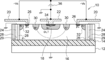
- FIG. 1A shows an example of a cross-sectional view of the semiconductor integrated circuit 10 according to the present embodiment
- FIG. 1B shows an example of a plan view of the semiconductor integrated circuit 10.
- FIG. 1A is a cross-sectional view of the semiconductor integrated circuit 10 cut along the line AA'shown in FIG. 1B. However, in FIG. 1B, a part of the configuration shown in FIG. 1A is omitted.
- the semiconductor integrated circuit 10 includes a semiconductor substrate 12, an embedded insulating film 14, a P-type impurity region 16, an N-type impurity region 18, an anode electrode 20, and a cathode electrode 22.
- the semiconductor integrated circuit 10 is manufactured using an SOI wafer as an example. That is, the semiconductor substrate 12 is, for example, a P-type (P ⁇ ) silicon substrate, and the embedded insulating film 14 is a so-called BOX layer. Each of the P-type impurity region 16 (P ⁇ ) and the N-type impurity region 18 (N ⁇ ) is formed on the silicon semiconductor layer contained in the SOI wafer.
- the P-type impurity region 16 is a part of the layer constituting the anode of the semiconductor integrated circuit 10, and is connected to the anode electrode 20 via the P + contact region 26.
- the N-type impurity region 18 is a part of the layer constituting the cathode of the semiconductor integrated circuit 10, and is connected to the cathode electrode 22 via the N + contact region 34.
- a PN junction is formed at the interface between the P-type impurity region 16 and the N-type impurity region 18.
- P- is a P-type impurity region having a relatively low concentration
- P + is a P-type impurity region having a relatively high concentration
- N- is an N-type impurity region having a relatively low concentration.
- N + means each of the N-type impurity regions having a relatively high concentration.
- the semiconductor integrated circuit 10 further includes a polysilicon 24 and an oxide film 28.
- the polysilicon 24 is formed by filling the trench 29 (groove) formed in the silicon semiconductor layer of the SOI wafer.
- the trench 29 according to the present embodiment has a depth of reaching the embedded insulating film 14 as an example.
- the oxide film 28 is formed on the inner wall including the bottom of the trench 29 by using, for example, a silicon oxide film (SiO2).
- the trench 29 allows, for example, the semiconductor integrated circuit 10 to be easily separated from other circuit elements.
- a bias voltage ground potential in the present embodiment
- the "polysilicon 24" is an example of the "conductor" according to the present disclosure.
- the semiconductor integrated circuit 10 is further configured to include an N-impurity region 30 and an N-impurity region 32, and details of the N-impurity region 30 and the N-impurity region 32 will be described later.
- the semiconductor integrated circuit 10 has a track shape in which semicircles are connected to both sides of a rectangular portion in a plan view.
- the N-impurity region 30 is formed surrounding the N-type impurity region 18, the P + contact region 26 is formed surrounding the N-impurity region 30, and the polysilicon 24 is formed surrounding the P + contact region 26. ..
- the N-impurity region 32 which is not shown in FIG. 1B, is also formed between the P + contact region 26 and the polysilicon 24 so as to surround the P + contact region 26.
- the cathode electrode 22 is arranged so as to be surrounded by a plurality of impurity regions. Therefore, when the semiconductor integrated circuit 10 is mounted on a package or the like, the cathode electrode 22 is connected to an external terminal by using, for example, a bonding wire. That is, the cathode electrode 22 has the function of an electrode pad.
- the anode electrode 20 has a configuration in which it is extended to the outside of the semiconductor integrated circuit 10, and is connected to the electrode pad at the extension destination.
- FIG. 2 shows a method of connecting the power supply 36 when a negative bias (reverse bias) is applied as an example of a method of applying a bias voltage. That is, as shown in FIG. 2, the positive electrode of the power supply 36 is connected to the cathode electrode 22 connected to the GND (ground), and the negative electrode is connected to the anode electrode 20. At this time, the semiconductor substrate 12 and the polysilicon 24 are also connected to the GND.
- a negative bias reverse bias
- the voltage of the power supply 36 is Vb
- the voltage ⁇ Vb is applied to the anode electrode 20 and the potential of the cathode electrode 22 is 0V. Therefore, the potential difference between the terminals of the semiconductor integrated circuit 10 as a diode is Vb. It becomes.
- the negative bias is applied to the semiconductor integrated circuit 10 shown in FIG. 2, for example, when the semiconductor integrated circuit 10 is used as an electrostatic protection element.
- a PN junction is formed at the interface between the P-type impurity region 16 and the N-type impurity region 18.
- a depletion layer DLT is formed starting from the PN junction.
- the semiconductor layer (active layer) forming the diode is a P-type P-type impurity region 16. Therefore, when a negative bias is applied to the semiconductor substrate 12 having the GND potential opposite to each other with the embedded insulating film 14 in between, the P-type impurity region 16 is depleted to the vicinity of the interface in contact with the embedded insulating film 14, and the semiconductor substrate 12 and the semiconductor substrate 12 are depleted.
- the film thickness of the embedded insulating film 14 (BOX layer) can be made thinner (for example, to about 4 ⁇ m) as compared with the prior art. This point is fundamentally different from the semiconductor device according to JP-A-2004-335922, which has an insulating structure in contact with the BOX layer 2 to ensure a withstand voltage.
- the semiconductor integrated circuit 10 has a configuration in which breakdown is suppressed even in the vicinity of the trench 29, similar to the above effect. That is, since a negative potential is applied to the P-type impurity region 16 and the polysilicon 24 is connected to the GND, the P-type impurity region 16 is depleted via the oxide film 28, and the peripheral portion of the P-type impurity region 16 is depleted. Breakdown is suppressed. That is, the semiconductor integrated circuit 10 is configured such that a depletion layer is formed over the entire P-type impurity region 16. As a result, a high withstand voltage can be ensured even with an embedded insulating film 14 (BOX layer) having a film thickness thinner than that of the prior art (for example, 4 ⁇ m).
- BOX layer embedded insulating film 14
- the N-impurity region 30 shown in FIG. 2 has a function as an electric field relaxation layer. That is, the N-impurity region 30 has the same effect on the depletion layer DLT as the N-type impurity region 18, and has an effect of expanding the depletion layer DLT. That is, the N-impurity region 30 is integrated with the depletion layer DLT formed for the N-type impurity region 18 and further combined with the depletion layer in the vicinity of the trench 29 described above, so that the depletion layer DLT is laterally oriented (FIG. It has the effect of spreading in the left-right direction of the paper surface of 2.
- the N-impurity region 30 may be provided in consideration of the withstand voltage required for the semiconductor integrated circuit 10, and is not essential.
- a negative bias is applied to the wiring of the anode electrode 20, and the P + layer (P + contact region 26) and the P- layer (P-type impurity region 16) near the surface of the semiconductor integrated circuit 10 become equipotential. There is. Therefore, in the semiconductor integrated circuit 10 according to the present embodiment, the bias effect due to the wiring (anode electrode 20) is not easily received. However, in the peripheral portion of the semiconductor integrated circuit 10, the potential of the P-type impurity region 16 is higher (closer to GND) than the wiring of the anode electrode 20.
- the P-type accumulation effect is generated and the P-type accumulation effect region comes into contact with the depletion layer DLT in the peripheral portion of the trench 29, so that the withstand voltage of the semiconductor integrated circuit 10 is lowered.
- an N-impurity region 32 is formed in the peripheral portion of the trench 29 in order to suppress breakdown due to this mechanism. That is, the N-impurity region 32 has a function as a channel stopper.
- the "bias effect” or “accumulation effect” is also called the "MOS effect” and means that a charge inversion layer is formed in the semiconductor layer below the wiring.
- the N-impurity region 32 may be provided in consideration of the withstand voltage required for the semiconductor integrated circuit 10, and is not essential.
- the semiconductor integrated circuit 10 has a track shape as shown in FIG. 1B in a plan view in order to effectively show the effect of the above-mentioned structure. That is, by forming the semiconductor integrated circuit 10 into a track shape, the cross-sectional structures in various directions can be made into the cross-sectional structure shown in FIG. 1A. That is, by eliminating the direction dependence of the cross-sectional structure of the semiconductor integrated circuit 10, the depletion layer DLT expands isotropically, and the effect of improving the withstand voltage can be equally exerted in any direction.
- the shape of the semiconductor integrated circuit 10 in a plan view is illustrated and described, but the present invention is not limited to this, and other shapes such as a circular shape and an elliptical shape are used. May be. However, it is preferable that the shape has no corners.
- the structure of the SOI wafer is not complicated as in the prior art, and the structure occupies a smaller area. It is possible to configure a semiconductor integrated circuit (diode) capable of ensuring high withstand voltage.
- the embodiment using the P-type semiconductor substrate has been described as an example in the above embodiment, the embodiment using the N-type substrate may be used.
- P type may be read as N type and N type may be read as P type.
Landscapes
- Element Separation (AREA)
- Metal-Oxide And Bipolar Metal-Oxide Semiconductor Integrated Circuits (AREA)
Abstract
第1導電型の基板と、基板上に設けられた埋め込み絶縁膜と、埋め込み絶縁膜上に設けられた第1導電型の活性層と、活性層内に形成された第2導電型の第1不純物領域と、第1不純物領域を囲んで活性層内に形成された第2導電型の電界緩和層と、電界緩和層を囲んで活性層内に形成された第1導電型の第2不純物領域と、第2不純物領域を囲んで形成され、埋め込み絶縁膜に達する溝と、を含む半導体集積回路が提供される。
Description
本開示は、半導体集積回路、特に、SOI構造を有する高耐圧ダイオードを含む半導体集積回路に関する。
高耐圧ダイオードに関する従来技術として、例えば特開2004-335922号公報に開示された半導体装置が知られている。特開2004-335922号公報の記載に係る半導体装置は、BOX(Buried Oxide:埋め込み絶縁膜)層2上の半導体層10に、第1のP型領域11、N+型領域12、N-型領域13から成るダイオードが形成されている。半導体層10の底部には第2のP型領域14が形成され、当該第2のP型領域14は絶縁酸化膜21により複数に分割されている。本構成において、ダイオードが逆バイアス状態にあるとき、N+型領域12真下の第2のP型領域14はほぼ第1のN+型領域12と同一の電圧となる。そして第1のP型領域11に近づくにつれて第2のP型領域14の電位が低くなる。その結果、半導体層10とBOX層2との界面における電界集中が緩和され、当該ダイオードの高耐圧化を図ることができるとしている。
しかしながら、上記特開2004-335922号公報に係る半導体装置では、絶縁酸化膜21により複数に分割された第2のP型領域14という特殊な構造が必要になるため、SOI(Silicon On Insulator)ウェハの製造工程が複雑になり、その結果コストが高くなる、という問題がある。また、特開2004-335922号公報に係る半導体装置は、構造が複雑なので、小型化の観点からも改善の余地がある。さらに、N-型領域13がBOX層2と接触する構造となっているため、ダイオードに負バイアスを印加した際に空乏化せず、BOX層2の膜厚が薄い場合には、耐圧を確保することが困難となるという問題がある。
一般に、BOX層の許容電圧はBOX層の膜厚に依存し、膜厚が厚い方が、許容電圧が大きい。一方、BOX層の膜厚は製造プロセス等に依存し、採用できる膜厚には自ずと限界がある。すなわち、BOX層が負担できる電圧にも限界がある。この点、特開2004-335922号公報に係るダイオードでは、BOX層の負担電圧以上の耐圧を確保することが困難となっているため、BOX層の膜厚を厚くせざるをえない(例えば、6μm程度)という問題があった。
従って、BOX層の膜厚を抑えたSOI構造を有する半導体集積回路において、小型化が可能な簡易な構成で、例えば負バイアスを印加した際に、十分な耐圧を確保することができる半導体集積回路、特にダイオードが求められていた。
本開示の実施形態は、上記事実を考慮し、簡易な構成で耐圧を向上させ、小型化が可能な半導体集積回路を提供することを目的とする。
本開示の第1実施態様に係る半導体集積回路は、第1導電型の基板と、基板上に設けられた埋め込み絶縁膜と、埋め込み絶縁膜上に設けられた第1導電型の活性層と、活性層内に形成された第2導電型の第1不純物領域と、第1不純物領域を囲んで活性層内に形成された第2導電型の電界緩和層と、電界緩和層を囲んで活性層内に形成された第1導電型の第2不純物領域と、第2不純物領域を囲んで形成され、前記埋め込み絶縁膜に達する溝と、を含んでいる。
第1実施態様に係る半導体集積回路は、埋め込み絶縁膜と、埋め込み絶縁膜上に形成された第1導電型の活性層と、活性層内に形成された第2導電型の第1不純物領域と、を含む。
ここで、第1導電型の活性層と第2導電型の第1不純物領域の界面にはPN接合が存在し、ダイオードが形成されている。そして、第2導電型の電界緩和層が第1不純物領域を囲んでさらに設けられているので空乏層が拡張され、その結果耐圧の向上を図ることができる。
本開示の第2実施態様に係る半導体集積回路では、第1実施態様に係る半導体集積回路において、溝の内面に形成された酸化膜と、第2不純物領域を囲むとともに酸化膜に隣接して活性層内に形成された第2導電型の第3不純物領域と、をさらに含んでいる。
第2実施態様に係る半導体集積回路によれば、酸化膜と、第2不純物領域を囲むとともに酸化膜に隣接して活性層内に形成された第2導電型の第3不純物領域と、をさらに含んでいる。そして、第3不純物領域がチャネルストッパとして機能するので、耐圧の低下が抑制される。
本開示の第3実施態様に係る半導体集積回路では、第2実施態様に係る半導体集積回路において、酸化膜を介して溝の内部に形成された導電体をさらに含み、第1不純物領域および導電体に第1電位を付与し、第2不純物領域に第1電位より低い第2電位を付与した場合に、活性層の全体に亘って空乏層が形成される。
第3実施態様に係る半導体集積回路によれば、第1不純物領域および導電体に第1電位を付与し、第2不純物領域に第1電位より低い第2電位を付与した場合に、活性層の全体に亘って空乏層が形成される。このため、負バイアスを印加した場合に、活性層全体が空乏化され、さらに効率的に耐圧の向上を図ることができる。
本開示の第4実施態様に係る半導体集積回路では、第2実施態様または第3実施態様に係る半導体集積回路において、基板の平面視での外形形状がトラック形状であり、電界緩和層、第2不純物領域、溝、および第3不純物領域の各々が、基板の外形形状に沿ってトラック形状に形成されている。
第4実施態様に係る半導体集積回路によれば、半導体集積回路全体がトラック形状に形成されている。このため、半導体集積回路の断面方向に依存することなく耐圧の向上を図ることができる。
本開示の第5実施態様に係る半導体集積回路では、第1実施態様から第4実施態様のいずれか1つに係る半導体集積回路において、第1導電型がP型であり、第2導電型がN型である。
第5実施態様に係る半導体集積回路によれば、活性層がP型となる。このため、カソード領域を囲んでアノード領域が配置された半導体集積回路を構成することができる。
本開示の実施形態によれば、簡易な構成で耐圧を向上させ、小型化が可能な半導体集積回路を提供することができる、という優れた効果を奏する。
以下、図1A、図1Bおよび図2を参照して、本開示の一実施の形態に係る半導体集積回路について説明する。以下の実施の形態では、本開示に係る半導体集積回路を高耐圧ダイオードに適用した形態を例示して説明する。また、本実施の形態に係る半導体集積回路は、一例としてSOIウェハを用いたDTI(Deep Trench Isolation)技術を採用して製造される。つまり、本実施の形態に係る半導体集積回路は、SOIウェハのBOX層に達するトレンチ(溝)を備えている。ここで、本実施の形態では、「高耐圧」の具体的な電圧の一例として、600V以上を想定している。なお、各図面において同一または等価な構成要素および部分には同一の参照符号を付与し、重複する説明は適宜省略する。
図1Aは、本実施の形態に係る半導体集積回路10の断面図の一例を、図1Bは半導体集積回路10の平面図の一例を示している。図1Aは、図1Bに示すA-A’線で切断した半導体集積回路10の断面図である。ただし、図1Bでは、図1Aに示す構成の一部を省略して図示している。図1Aに示すように、半導体集積回路10は、半導体基板12、埋め込み絶縁膜14、P型不純物領域16、N型不純物領域18、アノード電極20、およびカソード電極22を含んで構成されている。
本実施の形態に係る半導体集積回路10は、上述したように、一例としてSOIウェハを用いて製造されている。すなわち、半導体基板12は、一例としてP型(P-)のシリコン基板とされて、埋め込み絶縁膜14はいわゆるBOX層である。P型不純物領域16(P-)、N型不純物領域18(N-)の各々は、SOIウェハに含まれるシリコン半導体層に形成されている。P型不純物領域16は半導体集積回路10のアノードを構成する層の一部であり、P+コンタクト領域26を介してアノード電極20に接続されている。
N型不純物領域18は半導体集積回路10のカソードを構成する層の一部であり、N+コンタクト領域34を介してカソード電極22に接続されている。P型不純物領域16とN型不純物領域18との界面には、PN接合が形成されている。ここで、本実施の形態では、P-は比較的低い濃度のP型不純物領域を、P+は比較的濃度の高いP型不純物領域を、N-は比較的低い濃度のN型不純物領域を、N+は比較的濃度の高いN型不純物領域を、各々意味している。
N型不純物領域18は半導体集積回路10のカソードを構成する層の一部であり、N+コンタクト領域34を介してカソード電極22に接続されている。P型不純物領域16とN型不純物領域18との界面には、PN接合が形成されている。ここで、本実施の形態では、P-は比較的低い濃度のP型不純物領域を、P+は比較的濃度の高いP型不純物領域を、N-は比較的低い濃度のN型不純物領域を、N+は比較的濃度の高いN型不純物領域を、各々意味している。
半導体集積回路10は、さらに、ポリシリコン24、および酸化膜28を含んでいる。
ポリシリコン24は、SOIウェハのシリコン半導体層に形成されたトレンチ29(溝)を充填して形成されている。本実施の形態に係るトレンチ29は、一例として、埋め込み絶縁膜14に到達する深さを有している。酸化膜28は、例えばシリコン酸化膜(SiO2)を用いてトレンチ29の底部を含む内壁に形成されている。トレンチ29によって、例えば半導体集積回路10を他の回路素子から容易に分離することができる。ポリシリコン24をトレンチ29に充填することにより、後述するように埋め込み絶縁膜14に連なるポリシリコン24にバイアス電圧(本実施の形態では接地電位)を印加することができる。なお、「ポリシリコン24」は、本開示に係る「導電体」の一例である。
ポリシリコン24は、SOIウェハのシリコン半導体層に形成されたトレンチ29(溝)を充填して形成されている。本実施の形態に係るトレンチ29は、一例として、埋め込み絶縁膜14に到達する深さを有している。酸化膜28は、例えばシリコン酸化膜(SiO2)を用いてトレンチ29の底部を含む内壁に形成されている。トレンチ29によって、例えば半導体集積回路10を他の回路素子から容易に分離することができる。ポリシリコン24をトレンチ29に充填することにより、後述するように埋め込み絶縁膜14に連なるポリシリコン24にバイアス電圧(本実施の形態では接地電位)を印加することができる。なお、「ポリシリコン24」は、本開示に係る「導電体」の一例である。
半導体集積回路10は、さらにN-不純物領域30、およびN-不純物領域32を含んで構成されているが、N-不純物領域30、およびN-不純物領域32の詳細については後述する。
図1Bに示すように、本実施の形態に係る半導体集積回路10は、平面視で、矩形部分の両側に半円形を接続した、トラック形状をなしている。そして、N-不純物領域30はN型不純物領域18を囲んで形成され、P+コンタクト領域26はN-不純物領域30を囲んで形成され、ポリシリコン24はP+コンタクト領域26を囲んで形成されている。
なお、図1Bで図示を省略しているN-不純物領域32も、P+コンタクト領域26を囲んで、P+コンタクト領域26とポリシリコン24の間に形成されている。
なお、図1Bで図示を省略しているN-不純物領域32も、P+コンタクト領域26を囲んで、P+コンタクト領域26とポリシリコン24の間に形成されている。
図1Bに示すように、半導体集積回路10では、カソード電極22が複数の不純物領域で囲まれて配置されている。従って、半導体集積回路10をパッケージ等に実装する場合には、カソード電極22は例えばボンディングワイヤを用いて外部端子と接続される。つまり、カソード電極22は、電極パッドの機能を有する。これに対しアノード電極20は、図1Bに示すように、半導体集積回路10の外部まで延伸された構成となっており、延伸先で電極パッドに接続される。
次に、図2を参照して、半導体集積回路10へのバイアス電圧の印加方法について説明する。図2は、バイアス電圧の印加方法の一例として、負バイアス(逆バイアス)を印加する場合の電源36の接続方法を示している。すなわち、図2に示すように、電源36の正極を、GND(グランド)に接続されたカソード電極22に接続し、負極をアノード電極20に接続する。この際、半導体基板12、およびポリシリコン24もGNDに接続する。
この場合、電源36の電圧をVbとすると、アノード電極20には電圧-Vbが印加され、カソード電極22の電位が0Vであることから、ダイオードとしての半導体集積回路10の端子間の電位差はVbとなる。なお、図2に示す半導体集積回路10への負バイアスの印加は、例えば半導体集積回路10を静電保護素子として用いる場合に行う。
ここで、半導体集積回路10では、P型不純物領域16とN型不純物領域18との界面にPN接合が形成されている。図2に示すように、半導体集積回路10に負バイアスを印加すると、該PN接合を起点として空乏層DLTが形成される。半導体集積回路10では、ダイオードを形成する半導体層(活性層)がP型のP型不純物領域16とされている。
そのため、埋め込み絶縁膜14を挟んで対向するGND電位の半導体基板12に対して負バイアスが印加されると、P型不純物領域16が埋め込み絶縁膜14と接する界面付近まで空乏化し、半導体基板12とP型不純物領域16との間の電位差に起因するブレークダウンが抑制される。このため、埋め込み絶縁膜14(BOX層)の膜厚を従来技術に比較して薄くする(例えば、4μm程度まで薄くする)ことが可能となっている。この点が、BOX層2と接する絶縁構造で耐圧を確保する構造となっている、上述の特開2004-335922号公報に係る半導体装置と根本的に異なる点である。
そのため、埋め込み絶縁膜14を挟んで対向するGND電位の半導体基板12に対して負バイアスが印加されると、P型不純物領域16が埋め込み絶縁膜14と接する界面付近まで空乏化し、半導体基板12とP型不純物領域16との間の電位差に起因するブレークダウンが抑制される。このため、埋め込み絶縁膜14(BOX層)の膜厚を従来技術に比較して薄くする(例えば、4μm程度まで薄くする)ことが可能となっている。この点が、BOX層2と接する絶縁構造で耐圧を確保する構造となっている、上述の特開2004-335922号公報に係る半導体装置と根本的に異なる点である。
また、半導体集積回路10では、上記効果と同様に、トレンチ29の近傍でもブレークダウンが抑制される構成となっている。すなわち、P型不純物領域16に負電位が印加され、ポリシリコン24がGNDに接続されているので、酸化膜28を介してP型不純物領域16が空乏化され、P型不純物領域16の周縁部でのブレークダウンが抑制されている。すなわち、半導体集積回路10では、P型不純物領域16の全体に亘って空乏層が形成されるように構成されている。その結果、従来技術より膜厚の薄い(例えば、4μm)埋め込み絶縁膜14(BOX層)でも高耐圧を確保することができる。
図2に示すN-不純物領域30は、電界緩和層としての機能を有する。すなわち、N-不純物領域30は空乏層DLTに対してN型不純物領域18と同様の作用を有し、空乏層DLTを拡大する作用を奏する。つまり、N-不純物領域30は、N型不純物領域18に対して形成された空乏層DLTと一体化され、さらに上述したトレンチ29の近傍の空乏層と結合され、空乏層DLTを横方向(図2の紙面左右方向)に広げる作用を有する。なお、N-不純物領域30は、半導体集積回路10に求められる耐圧等を勘案して設ければよいもので、必須のものではない。
アノード電極20の配線には負バイアスが印加されており、半導体集積回路10の表面付近のP+層(P+コンタクト領域26)、およびP-層(P型不純物領域16)は、等電位となっている。そのため、本実施の形態に係る半導体集積回路10では、配線(アノード電極20)によるバイアス効果は受けにくい。ただし、半導体集積回路10の周縁部では、P型不純物領域16の電位がアノード電極20の配線と比較して高く(GNDに近く)なっている。そのため、P型蓄積効果が発生し、該P型蓄積効果領域がトレンチ29の周辺部における空乏層DLTと接することによって、半導体集積回路10の耐圧が低下することも想定される。半導体集積回路10では、このメカニズムのよるブレークダウンを抑制するため、トレンチ29の周辺部にN-不純物領域32を形成している。つまり、N-不純物領域32はチャネルストッパとしての機能を有する。ここで、「バイアス効果」、あるいは「蓄積効果」とは、「MOS効果」ともよばれ、配線の下部の半導体層に電荷の反転層が形成されることをいう。なお、N-不純物領域32は、半導体集積回路10に求められる耐圧等を勘案して設ければよいもので、必須のものではない。
本実施の形態に係る半導体集積回路10は、上述した構造による効果を有効あらしめるために、平面視での形状を図1Bに示すようなトラック形状としている。すなわち、半導体集積回路10をトラック形状とすることで、様々な方向の断面構造を図1Aに示す断面構造とすることができる。つまり、半導体集積回路10の断面構造の方向依存性をなくすことにより、空乏層DLTが等方的に拡がり、どの方向に対しても等しく耐圧向上の効果を発揮させることができる。なお、本実施の形態では、半導体集積回路10の平面視での形状をトラック形状とする形態を例示して説明したが、これに限られず、円形状、楕円形状等他の形状を用いた形態としてもよい。ただし、当該形状は角を有さないことが好ましい。
以上詳述したように、上記構成を有する本実施の形態に係る半導体集積回路によれば、従来技術のようにSOIウェハの構造を複雑な構造とすることなく、また、占有面積のより小さい構造で高耐圧を確保することが可能な半導体集積回路(ダイオード)を構成することができる。
なお、上記実施の形態では、P型の半導体基板を用いた形態を例示して説明したが、N型基板を用いた形態としてもよい。この場合は、上記において、P型をN型に、N型をP型に読み替えればよい。
2019年11月1日に出願された日本国特許出願2019-200243号の開示は、その全体が参照により本明細書に取り込まれる。
本明細書に記載された全ての文献、特許出願、および技術規格は、個々の文献、特許出願、および技術規格が参照により取り込まれることが具体的かつ個々に記された場合と同程度に、本明細書中に参照により取り込まれる。
Claims (5)
- 第1導電型の基板と、
前記基板上に設けられた埋め込み絶縁膜と、
前記埋め込み絶縁膜上に設けられた第1導電型の活性層と、
前記活性層内に形成された第2導電型の第1不純物領域と、
前記第1不純物領域を囲んで前記活性層内に形成された第2導電型の電界緩和層と、
前記電界緩和層を囲んで前記活性層内に形成された第1導電型の第2不純物領域と、
前記第2不純物領域を囲んで形成され、前記埋め込み絶縁膜に達する溝と、
を含む半導体集積回路。 - 前記溝の内面に形成された酸化膜と、
前記第2不純物領域を囲むとともに前記酸化膜に隣接して前記活性層内に形成された第2導電型の第3不純物領域と、をさらに含む
請求項1に記載の半導体集積回路。 - 前記酸化膜を介して前記溝の内部に形成された導電体をさらに含み、
前記基板、前記第1不純物領域、および前記導電体に第1電位を付与し、前記第2不純物領域に前記第1電位より低い第2電位を付与した場合に、前記活性層の全体に亘って空乏層が形成される
請求項2に記載の半導体集積回路。 - 前記基板の平面視での外形形状がトラック形状であり、
前記電界緩和層、前記第2不純物領域、前記溝、および前記第3不純物領域の各々が、前記基板の外形形状に沿ってトラック形状に形成されている
請求項2または請求項3に記載の半導体集積回路。 - 前記第1導電型がP型であり、前記第2導電型がN型である
請求項1から請求項4のいずれか1項に記載の半導体集積回路。
Priority Applications (2)
| Application Number | Priority Date | Filing Date | Title |
|---|---|---|---|
| US17/771,134 US11973146B2 (en) | 2019-11-01 | 2020-10-27 | Semiconductor integrated circuit |
| CN202080073210.7A CN114556586A (zh) | 2019-11-01 | 2020-10-27 | 半导体集成电路 |
Applications Claiming Priority (2)
| Application Number | Priority Date | Filing Date | Title |
|---|---|---|---|
| JP2019200243A JP7404600B2 (ja) | 2019-11-01 | 2019-11-01 | 半導体集積回路 |
| JP2019-200243 | 2019-11-01 |
Publications (1)
| Publication Number | Publication Date |
|---|---|
| WO2021085437A1 true WO2021085437A1 (ja) | 2021-05-06 |
Family
ID=75713471
Family Applications (1)
| Application Number | Title | Priority Date | Filing Date |
|---|---|---|---|
| PCT/JP2020/040320 Ceased WO2021085437A1 (ja) | 2019-11-01 | 2020-10-27 | 半導体集積回路 |
Country Status (4)
| Country | Link |
|---|---|
| US (1) | US11973146B2 (ja) |
| JP (1) | JP7404600B2 (ja) |
| CN (1) | CN114556586A (ja) |
| WO (1) | WO2021085437A1 (ja) |
Citations (3)
| Publication number | Priority date | Publication date | Assignee | Title |
|---|---|---|---|---|
| JPH01103851A (ja) * | 1987-02-26 | 1989-04-20 | Toshiba Corp | 高耐圧半導体素子 |
| JPH05136436A (ja) * | 1991-01-31 | 1993-06-01 | Toshiba Corp | 高耐圧半導体素子 |
| JP2013084903A (ja) * | 2011-09-27 | 2013-05-09 | Denso Corp | 横型素子を有する半導体装置 |
Family Cites Families (16)
| Publication number | Priority date | Publication date | Assignee | Title |
|---|---|---|---|---|
| US5294825A (en) | 1987-02-26 | 1994-03-15 | Kabushiki Kaisha Toshiba | High breakdown voltage semiconductor device |
| US5241210A (en) * | 1987-02-26 | 1993-08-31 | Kabushiki Kaisha Toshiba | High breakdown voltage semiconductor device |
| EP1138082A1 (en) * | 1999-09-16 | 2001-10-04 | Koninklijke Philips Electronics N.V. | Semiconductor device |
| JP4204895B2 (ja) | 2003-05-12 | 2009-01-07 | 三菱電機株式会社 | 半導体装置 |
| US7095092B2 (en) * | 2004-04-30 | 2006-08-22 | Freescale Semiconductor, Inc. | Semiconductor device and method of forming the same |
| US7582916B2 (en) * | 2008-01-14 | 2009-09-01 | United Microelectronics Corp. | Silicon controlled rectifier |
| JP5172654B2 (ja) * | 2008-12-27 | 2013-03-27 | 株式会社東芝 | 半導体装置 |
| JP5458809B2 (ja) * | 2009-11-02 | 2014-04-02 | 富士電機株式会社 | 半導体装置 |
| JP5711646B2 (ja) * | 2010-11-16 | 2015-05-07 | 株式会社豊田中央研究所 | ダイオード |
| JP5757145B2 (ja) * | 2011-04-19 | 2015-07-29 | 富士電機株式会社 | 半導体装置 |
| CN103094359B (zh) * | 2011-10-31 | 2016-05-11 | 无锡华润上华半导体有限公司 | 高压肖特基二极管及其制作方法 |
| JP6098041B2 (ja) * | 2012-04-02 | 2017-03-22 | 富士電機株式会社 | 半導体装置 |
| JP2014103342A (ja) * | 2012-11-22 | 2014-06-05 | Nippon Inter Electronics Corp | 半導体装置 |
| WO2015104900A1 (ja) * | 2014-01-10 | 2015-07-16 | 三菱電機株式会社 | 半導体装置 |
| US10217733B2 (en) * | 2015-09-15 | 2019-02-26 | Semiconductor Components Industries, Llc | Fast SCR structure for ESD protection |
| FR3094837B1 (fr) * | 2019-04-05 | 2022-09-09 | St Microelectronics Tours Sas | Dispositif de protection contre des décharges électrostatiques |
-
2019
- 2019-11-01 JP JP2019200243A patent/JP7404600B2/ja active Active
-
2020
- 2020-10-27 US US17/771,134 patent/US11973146B2/en active Active
- 2020-10-27 CN CN202080073210.7A patent/CN114556586A/zh active Pending
- 2020-10-27 WO PCT/JP2020/040320 patent/WO2021085437A1/ja not_active Ceased
Patent Citations (3)
| Publication number | Priority date | Publication date | Assignee | Title |
|---|---|---|---|---|
| JPH01103851A (ja) * | 1987-02-26 | 1989-04-20 | Toshiba Corp | 高耐圧半導体素子 |
| JPH05136436A (ja) * | 1991-01-31 | 1993-06-01 | Toshiba Corp | 高耐圧半導体素子 |
| JP2013084903A (ja) * | 2011-09-27 | 2013-05-09 | Denso Corp | 横型素子を有する半導体装置 |
Also Published As
| Publication number | Publication date |
|---|---|
| JP2021072426A (ja) | 2021-05-06 |
| US11973146B2 (en) | 2024-04-30 |
| CN114556586A (zh) | 2022-05-27 |
| JP7404600B2 (ja) | 2023-12-26 |
| US20220302323A1 (en) | 2022-09-22 |
Similar Documents
| Publication | Publication Date | Title |
|---|---|---|
| US7906813B2 (en) | Semiconductor device having a first circuit block isolating a plurality of circuit blocks | |
| JP4206543B2 (ja) | 半導体装置 | |
| JP5458809B2 (ja) | 半導体装置 | |
| KR101128716B1 (ko) | 반도체 장치 | |
| KR100726898B1 (ko) | 유전체 분리형 반도체 장치 | |
| TWI775235B (zh) | 橫向雙擴散金氧半電晶體以及n型通道橫向雙擴散金氧半電晶體 | |
| KR100780967B1 (ko) | 고전압용 쇼트키 다이오드 구조체 | |
| CN103219360B (zh) | 半导体装置 | |
| JP7038518B2 (ja) | 半導体装置 | |
| US6642583B2 (en) | CMOS device with trench structure | |
| JPH01103851A (ja) | 高耐圧半導体素子 | |
| JP5331497B2 (ja) | 半導体装置およびその製造方法 | |
| JP3298455B2 (ja) | 半導体装置 | |
| KR101606374B1 (ko) | 반도체장치 | |
| US12159914B2 (en) | Trench power semiconductor device | |
| JP4961686B2 (ja) | 半導体装置 | |
| JP4864344B2 (ja) | 半導体装置 | |
| JP7404600B2 (ja) | 半導体集積回路 | |
| US20230223296A1 (en) | Semiconductor device and method of manufacturing semiconductor device | |
| JP7404601B2 (ja) | 半導体集積回路 | |
| KR20120004954A (ko) | 반도체 장치 | |
| JP5092202B2 (ja) | 半導体装置 | |
| TWI843431B (zh) | 靜電放電保護元件 | |
| JP2020205308A (ja) | 半導体装置 | |
| US11444074B2 (en) | Semiconductor device and method for manufacturing same |
Legal Events
| Date | Code | Title | Description |
|---|---|---|---|
| 121 | Ep: the epo has been informed by wipo that ep was designated in this application |
Ref document number: 20881101 Country of ref document: EP Kind code of ref document: A1 |
|
| NENP | Non-entry into the national phase |
Ref country code: DE |
|
| 122 | Ep: pct application non-entry in european phase |
Ref document number: 20881101 Country of ref document: EP Kind code of ref document: A1 |