WO2021085078A1 - 炭化珪素半導体装置および炭化珪素半導体装置の製造方法 - Google Patents
炭化珪素半導体装置および炭化珪素半導体装置の製造方法 Download PDFInfo
- Publication number
- WO2021085078A1 WO2021085078A1 PCT/JP2020/038231 JP2020038231W WO2021085078A1 WO 2021085078 A1 WO2021085078 A1 WO 2021085078A1 JP 2020038231 W JP2020038231 W JP 2020038231W WO 2021085078 A1 WO2021085078 A1 WO 2021085078A1
- Authority
- WO
- WIPO (PCT)
- Prior art keywords
- region
- silicon carbide
- main surface
- impurity
- impurity region
- Prior art date
- Legal status (The legal status is an assumption and is not a legal conclusion. Google has not performed a legal analysis and makes no representation as to the accuracy of the status listed.)
- Ceased
Links
Images


Classifications
-
- H—ELECTRICITY
- H10—SEMICONDUCTOR DEVICES; ELECTRIC SOLID-STATE DEVICES NOT OTHERWISE PROVIDED FOR
- H10D—INORGANIC ELECTRIC SEMICONDUCTOR DEVICES
- H10D64/00—Electrodes of devices having potential barriers
- H10D64/20—Electrodes characterised by their shapes, relative sizes or dispositions
- H10D64/23—Electrodes carrying the current to be rectified, amplified, oscillated or switched, e.g. sources, drains, anodes or cathodes
- H10D64/251—Source or drain electrodes for field-effect devices
- H10D64/256—Source or drain electrodes for field-effect devices for lateral devices wherein the source or drain electrodes are recessed in semiconductor bodies
-
- H—ELECTRICITY
- H10—SEMICONDUCTOR DEVICES; ELECTRIC SOLID-STATE DEVICES NOT OTHERWISE PROVIDED FOR
- H10D—INORGANIC ELECTRIC SEMICONDUCTOR DEVICES
- H10D30/00—Field-effect transistors [FET]
- H10D30/60—Insulated-gate field-effect transistors [IGFET]
- H10D30/64—Double-diffused metal-oxide semiconductor [DMOS] FETs
- H10D30/66—Vertical DMOS [VDMOS] FETs
- H10D30/668—Vertical DMOS [VDMOS] FETs having trench gate electrodes, e.g. UMOS transistors
-
- H—ELECTRICITY
- H10—SEMICONDUCTOR DEVICES; ELECTRIC SOLID-STATE DEVICES NOT OTHERWISE PROVIDED FOR
- H10D—INORGANIC ELECTRIC SEMICONDUCTOR DEVICES
- H10D62/00—Semiconductor bodies, or regions thereof, of devices having potential barriers
- H10D62/10—Shapes, relative sizes or dispositions of the regions of the semiconductor bodies; Shapes of the semiconductor bodies
- H10D62/124—Shapes, relative sizes or dispositions of the regions of semiconductor bodies or of junctions between the regions
-
- H—ELECTRICITY
- H10—SEMICONDUCTOR DEVICES; ELECTRIC SOLID-STATE DEVICES NOT OTHERWISE PROVIDED FOR
- H10D—INORGANIC ELECTRIC SEMICONDUCTOR DEVICES
- H10D12/00—Bipolar devices controlled by the field effect, e.g. insulated-gate bipolar transistors [IGBT]
- H10D12/01—Manufacture or treatment
- H10D12/031—Manufacture or treatment of IGBTs
-
- H—ELECTRICITY
- H10—SEMICONDUCTOR DEVICES; ELECTRIC SOLID-STATE DEVICES NOT OTHERWISE PROVIDED FOR
- H10D—INORGANIC ELECTRIC SEMICONDUCTOR DEVICES
- H10D30/00—Field-effect transistors [FET]
- H10D30/60—Insulated-gate field-effect transistors [IGFET]
- H10D30/63—Vertical IGFETs
- H10D30/635—Vertical IGFETs having no inversion channels, e.g. vertical accumulation channel FETs [ACCUFET] or normally-on vertical IGFETs
-
- H—ELECTRICITY
- H10—SEMICONDUCTOR DEVICES; ELECTRIC SOLID-STATE DEVICES NOT OTHERWISE PROVIDED FOR
- H10D—INORGANIC ELECTRIC SEMICONDUCTOR DEVICES
- H10D30/00—Field-effect transistors [FET]
- H10D30/60—Insulated-gate field-effect transistors [IGFET]
- H10D30/64—Double-diffused metal-oxide semiconductor [DMOS] FETs
- H10D30/66—Vertical DMOS [VDMOS] FETs
-
- H—ELECTRICITY
- H10—SEMICONDUCTOR DEVICES; ELECTRIC SOLID-STATE DEVICES NOT OTHERWISE PROVIDED FOR
- H10D—INORGANIC ELECTRIC SEMICONDUCTOR DEVICES
- H10D62/00—Semiconductor bodies, or regions thereof, of devices having potential barriers
- H10D62/10—Shapes, relative sizes or dispositions of the regions of the semiconductor bodies; Shapes of the semiconductor bodies
- H10D62/102—Constructional design considerations for preventing surface leakage or controlling electric field concentration
- H10D62/103—Constructional design considerations for preventing surface leakage or controlling electric field concentration for increasing or controlling the breakdown voltage of reverse-biased devices
- H10D62/105—Constructional design considerations for preventing surface leakage or controlling electric field concentration for increasing or controlling the breakdown voltage of reverse-biased devices by having particular doping profiles, shapes or arrangements of PN junctions; by having supplementary regions, e.g. junction termination extension [JTE]
- H10D62/109—Reduced surface field [RESURF] PN junction structures
- H10D62/111—Multiple RESURF structures, e.g. double RESURF or 3D-RESURF structures
-
- H—ELECTRICITY
- H10—SEMICONDUCTOR DEVICES; ELECTRIC SOLID-STATE DEVICES NOT OTHERWISE PROVIDED FOR
- H10D—INORGANIC ELECTRIC SEMICONDUCTOR DEVICES
- H10D62/00—Semiconductor bodies, or regions thereof, of devices having potential barriers
- H10D62/10—Shapes, relative sizes or dispositions of the regions of the semiconductor bodies; Shapes of the semiconductor bodies
- H10D62/124—Shapes, relative sizes or dispositions of the regions of semiconductor bodies or of junctions between the regions
- H10D62/125—Shapes of junctions between the regions
-
- H—ELECTRICITY
- H10—SEMICONDUCTOR DEVICES; ELECTRIC SOLID-STATE DEVICES NOT OTHERWISE PROVIDED FOR
- H10D—INORGANIC ELECTRIC SEMICONDUCTOR DEVICES
- H10D62/00—Semiconductor bodies, or regions thereof, of devices having potential barriers
- H10D62/10—Shapes, relative sizes or dispositions of the regions of the semiconductor bodies; Shapes of the semiconductor bodies
- H10D62/13—Semiconductor regions connected to electrodes carrying current to be rectified, amplified or switched, e.g. source or drain regions
- H10D62/149—Source or drain regions of field-effect devices
- H10D62/151—Source or drain regions of field-effect devices of IGFETs
- H10D62/156—Drain regions of DMOS transistors
- H10D62/157—Impurity concentrations or distributions
-
- H—ELECTRICITY
- H10—SEMICONDUCTOR DEVICES; ELECTRIC SOLID-STATE DEVICES NOT OTHERWISE PROVIDED FOR
- H10D—INORGANIC ELECTRIC SEMICONDUCTOR DEVICES
- H10D62/00—Semiconductor bodies, or regions thereof, of devices having potential barriers
- H10D62/10—Shapes, relative sizes or dispositions of the regions of the semiconductor bodies; Shapes of the semiconductor bodies
- H10D62/13—Semiconductor regions connected to electrodes carrying current to be rectified, amplified or switched, e.g. source or drain regions
- H10D62/149—Source or drain regions of field-effect devices
- H10D62/151—Source or drain regions of field-effect devices of IGFETs
- H10D62/156—Drain regions of DMOS transistors
- H10D62/159—Shapes
-
- H—ELECTRICITY
- H10—SEMICONDUCTOR DEVICES; ELECTRIC SOLID-STATE DEVICES NOT OTHERWISE PROVIDED FOR
- H10D—INORGANIC ELECTRIC SEMICONDUCTOR DEVICES
- H10D62/00—Semiconductor bodies, or regions thereof, of devices having potential barriers
- H10D62/10—Shapes, relative sizes or dispositions of the regions of the semiconductor bodies; Shapes of the semiconductor bodies
- H10D62/17—Semiconductor regions connected to electrodes not carrying current to be rectified, amplified or switched, e.g. channel regions
- H10D62/393—Body regions of DMOS transistors or IGBTs
-
- H—ELECTRICITY
- H10—SEMICONDUCTOR DEVICES; ELECTRIC SOLID-STATE DEVICES NOT OTHERWISE PROVIDED FOR
- H10D—INORGANIC ELECTRIC SEMICONDUCTOR DEVICES
- H10D62/00—Semiconductor bodies, or regions thereof, of devices having potential barriers
- H10D62/80—Semiconductor bodies, or regions thereof, of devices having potential barriers characterised by the materials
- H10D62/83—Semiconductor bodies, or regions thereof, of devices having potential barriers characterised by the materials being Group IV materials, e.g. B-doped Si or undoped Ge
- H10D62/832—Semiconductor bodies, or regions thereof, of devices having potential barriers characterised by the materials being Group IV materials, e.g. B-doped Si or undoped Ge being Group IV materials comprising two or more elements, e.g. SiGe
- H10D62/8325—Silicon carbide
-
- H—ELECTRICITY
- H10—SEMICONDUCTOR DEVICES; ELECTRIC SOLID-STATE DEVICES NOT OTHERWISE PROVIDED FOR
- H10D—INORGANIC ELECTRIC SEMICONDUCTOR DEVICES
- H10D62/00—Semiconductor bodies, or regions thereof, of devices having potential barriers
- H10D62/50—Physical imperfections
- H10D62/53—Physical imperfections the imperfections being within the semiconductor body
-
- H—ELECTRICITY
- H10—SEMICONDUCTOR DEVICES; ELECTRIC SOLID-STATE DEVICES NOT OTHERWISE PROVIDED FOR
- H10P—GENERIC PROCESSES OR APPARATUS FOR THE MANUFACTURE OR TREATMENT OF DEVICES COVERED BY CLASS H10
- H10P74/00—Testing or measuring during manufacture or treatment of wafers, substrates or devices
- H10P74/20—Testing or measuring during manufacture or treatment of wafers, substrates or devices characterised by the properties tested or measured, e.g. structural or electrical properties
- H10P74/203—Structural properties, e.g. testing or measuring thicknesses, line widths, warpage, bond strengths or physical defects
Definitions
- the present disclosure relates to a silicon carbide semiconductor device and a method for manufacturing a silicon carbide semiconductor device.
- This application claims priority based on Japanese Patent Application No. 2019-196257, which is a Japanese patent application filed on October 29, 2019. All the contents of the Japanese patent application are incorporated herein by reference.
- Non-Patent Document 1 The IV characteristics of the SiC-PiN diode are described.
- the silicon carbide semiconductor device includes a silicon carbide substrate, a first electrode, and a second electrode.
- the silicon carbide substrate has a first main surface, a second main surface opposite to the first main surface, a first impurity region which constitutes at least a part of the second main surface and has a first conductive type, and a first.
- the second impurity region which constitutes at least a part of one main surface and is provided in contact with the first impurity region and has a second conductive type different from the first conductive type, and the second impurity region so as to be separated from the first impurity region. It has a third impurity region that is provided in contact with the region and has a first conductive type.
- the first electrode is in contact with each of the second impurity region and the third impurity region on the first main surface.
- the second electrode is in contact with the first impurity region on the second main surface.
- the second impurity region includes a first region and a second region between the first region and the second main surface and in contact with the first region.
- the impurity concentration in the first region is 6 ⁇ 10 16 cm -3 or more.
- the silicon carbide semiconductor device includes a silicon carbide substrate, a first electrode, and a second electrode.
- the silicon carbide substrate has a first main surface, a second main surface opposite to the first main surface, a first impurity region which constitutes at least a part of the second main surface and has a first conductive type, and a first.
- the second impurity region which constitutes at least a part of one main surface and is provided in contact with the first impurity region and has a second conductive type different from the first conductive type, and the second impurity region so as to be separated from the first impurity region. It has a third impurity region that is provided in contact with the region and has a first conductive type.
- the first electrode is in contact with each of the second impurity region and the third impurity region on the first main surface.
- the second electrode is in contact with the first impurity region on the second main surface.
- the second impurity region includes a first region and a second region between the first region and the second main surface and in contact with the first region.
- the point defect density in the first region is 6 ⁇ 10 12 cm -3 or more.
- the method for manufacturing a silicon carbide semiconductor device includes the following steps.
- a silicon carbide substrate having a third impurity region having a first conductive type and a third impurity region is prepared.
- a first electrode is formed on the first main surface in contact with each of the second impurity region and the third impurity region.
- a second electrode in contact with the first impurity region is formed on the second main surface.
- the second impurity region includes a first region and a second region between the first region and the second main surface and in contact with the first region.
- the impurity concentration in the first region is 6 ⁇ 10 16 cm -3 or more.
- the first region is formed by ion implantation.
- FIG. 1 is a schematic cross-sectional view showing the configuration of the silicon carbide semiconductor device according to the first embodiment.
- FIG. 2 is a schematic cross-sectional view taken along the line II-II of FIG.
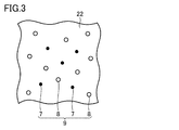
- FIG. 3 is an enlarged schematic view of region III of FIG.
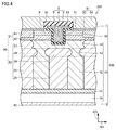
- FIG. 4 is a schematic cross-sectional view showing the configuration of the silicon carbide semiconductor device according to the second embodiment.
- FIG. 5 is a schematic cross-sectional view showing the configuration of the silicon carbide semiconductor device according to the third embodiment.
- FIG. 6 is a flowchart showing an outline of a method for manufacturing a silicon carbide semiconductor device according to the present embodiment.
- FIG. 1 is a schematic cross-sectional view showing the configuration of the silicon carbide semiconductor device according to the first embodiment.
- FIG. 2 is a schematic cross-sectional view taken along the line II-II of FIG.
- FIG. 3 is an enlarged schematic view of region III of FIG.
- FIG. 4 is a schematic cross-sectional view showing the configuration of the
- FIG. 7 is a flowchart showing an outline of a process of preparing a silicon carbide substrate in the method for manufacturing a silicon carbide semiconductor device according to the present embodiment.
- FIG. 8 is a schematic cross-sectional view showing the first step of the method for manufacturing the silicon carbide semiconductor device according to the present embodiment.
- FIG. 9 is a schematic cross-sectional view showing a second step of the method for manufacturing a silicon carbide semiconductor device according to the present embodiment.
- FIG. 10 is a schematic cross-sectional view showing a third step of the method for manufacturing a silicon carbide semiconductor device according to the present embodiment.
- FIG. 11 is a schematic cross-sectional view showing a fourth step of the method for manufacturing a silicon carbide semiconductor device according to the present embodiment.
- FIG. 8 is a schematic cross-sectional view showing the first step of the method for manufacturing the silicon carbide semiconductor device according to the present embodiment.
- FIG. 9 is a schematic cross-sectional view showing a second step of the method for manufacturing a silicon carbide semiconductor
- FIG. 12 is a schematic cross-sectional view showing a fifth step of the method for manufacturing a silicon carbide semiconductor device according to the present embodiment.
- FIG. 13 is a schematic cross-sectional view showing a sixth step of the method for manufacturing a silicon carbide semiconductor device according to the present embodiment.
- FIG. 14 is a schematic cross-sectional view showing a seventh step of the method for manufacturing a silicon carbide semiconductor device according to the present embodiment.
- FIG. 15 is a schematic cross-sectional view showing the eighth step of the method for manufacturing the silicon carbide semiconductor device according to the present embodiment. It is a figure which shows the relationship between the drain current density and the drain voltage in the silicon carbide semiconductor device which concerns on sample 1.
- FIG. It is a figure which shows the relationship between the drain current density and the drain voltage in the silicon carbide semiconductor device which concerns on sample 2.
- FIG. 12 is a schematic cross-sectional view showing a fifth step of the method for manufacturing a silicon carbide semiconductor device according to the present embodiment.
- FIG. 13 is a schematic
- An object of the present disclosure is to provide a silicon carbide semiconductor device and a method for manufacturing a silicon carbide semiconductor device capable of suppressing a temperature change in diode characteristics.
- a silicon carbide semiconductor device and a method for manufacturing a silicon carbide semiconductor device capable of suppressing a temperature change in diode characteristics are listed and described.
- the individual orientation is indicated by []
- the aggregation orientation is indicated by ⁇ >
- the individual plane is indicated by ()
- the aggregation plane is indicated by ⁇ .
- Negative crystallographic exponents are usually expressed by adding a "-" (bar) above the number, but here the number is preceded by a negative sign for crystallography. Represent the above negative exponent.
- the silicon carbide semiconductor device 200 includes a silicon carbide substrate 100, a first electrode 61, and a second electrode 62.
- the silicon carbide substrate 100 is a first surface that constitutes at least a part of a first main surface 1, a second main surface 2 opposite to the first main surface 1, and a second main surface 2 and has a first conductive type.
- An impurity region 10, a second impurity region 20 that constitutes at least a part of the first main surface 1 and is provided in contact with the first impurity region 10 and has a second conductive type different from the first conductive type, and a first impurity region.
- the second impurity region 20 includes a first region 21 and a second region 22 between the first region 21 and the second main surface 2 and in contact with the first region 21.
- the impurity concentration of the first region 21 is 6 ⁇ 10 16 cm -3 or more.
- the impurity concentration in the second region 22 may be 6 ⁇ 10 16 cm -3 or more.
- the silicon carbide semiconductor device 200 includes a silicon carbide substrate 100, a first electrode 61, and a second electrode 62.
- the silicon carbide substrate 100 is a first surface that constitutes at least a part of a first main surface 1, a second main surface 2 opposite to the first main surface 1, and a second main surface 2 and has a first conductive type.
- An impurity region 10, a second impurity region 20 that constitutes at least a part of the first main surface 1 and is provided in contact with the first impurity region 10 and has a second conductive type different from the first conductive type, and a first impurity region.
- the second impurity region 20 includes a first region 21 and a second region 22 between the first region 21 and the second main surface 2 and in contact with the first region 21.
- the point defect density of the first region 21 is 6 ⁇ 10 12 cm -3 or more.
- the point defect density of the first region 21 may be 1 ⁇ 10 14 cm -3 or less.
- the silicon carbide semiconductor device 200 may be a planar type.
- the silicon carbide substrate 100 may be provided with a trench 5. Even if the trench 5 has a side surface 3 in contact with each of the first impurity region 10, the second impurity region 20, and the third impurity region 30, and a bottom surface 4 connected to the side surface 3 and in contact with the first impurity region 10. Good.
- the shape of the trench 5 may be U-shaped in the cross section perpendicular to the first main surface 1.
- the shape of the trench 5 may be V-shaped in the cross section perpendicular to the first main surface 1.
- the first main surface 1 is 8 ° with respect to the (000-1) plane or the (000-1) plane.
- the surface may be inclined at the following angles.
- the impurity concentration in the first region 21 may be higher than the impurity concentration in the second region 22.
- the impurity concentration in the first region 21 may be 1 ⁇ 10 19 cm -3 or less.
- the method for manufacturing the silicon carbide semiconductor device 200 includes the following steps.
- the second impurity region 20 which constitutes at least a part of one main surface 1 and is provided in contact with the first impurity region 10 and has a second conductive type different from the first conductive type is separated from the first impurity region 10.
- a silicon carbide substrate 100 is prepared, which is provided in contact with the second impurity region 20 and has a third impurity region 30 having a first conductive type.
- a first electrode 61 in contact with each of the second impurity region 20 and the third impurity region 30 is formed on the first main surface 1.
- a second electrode 62 in contact with the first impurity region 10 is formed on the second main surface 2.
- the second impurity region 20 includes a first region 21 and a second region 22 between the first region 21 and the second main surface 2 and in contact with the first region 21.
- the impurity concentration of the first region 21 is 6 ⁇ 10 16 cm -3 or more.
- the first region 21 is formed by ion implantation.
- the second region 22 may be formed by ion implantation.
- the first impurity region 10 may be formed by epitaxial growth under temperature conditions of 1500 ° C. or higher and 1750 ° C. or lower. ..
- the step of preparing the silicon carbide substrate 100 may include an activation annealing step.
- the activation annealing step may be performed under temperature conditions of 1600 ° C. or higher and 1850 ° C. or lower.
- FIG. 1 is a schematic cross-sectional view showing the configuration of the silicon carbide semiconductor device 200 according to the first embodiment.
- the silicon carbide semiconductor device 200 is a trench-type MOSFET, and includes a silicon carbide substrate 100, a gate electrode 63, a gate insulating film 51, a separation insulating film 52, and the like. It mainly has a first electrode 61 and a second electrode 62.
- the silicon carbide substrate 100 has a first main surface 1 and a second main surface 2 opposite to the first main surface 1.
- the first main surface 1 is, for example, a surface that is 8 ° or less off from the ⁇ 0001 ⁇ surface or the ⁇ 0001 ⁇ surface. Specifically, the first main surface 1 is, for example, a surface inclined at an angle of 8 ° or less with respect to the (000-1) surface or the (000-1) surface. The first main surface 1 may be, for example, a (0001) surface or a surface inclined at an angle of 8 ° or less with respect to the (0001) surface.
- the silicon carbide substrate 100 includes a first impurity region 10, a second impurity region 20, and a third impurity region 30.
- the first impurity region 10 contains an n-type impurity that can impart an n-type such as N (nitrogen).
- the first impurity region 10 has, for example, an n-type (first conductive type).
- the first impurity region 10 constitutes at least a part of the second main surface 2. In other words, the first impurity region 10 may form the entire surface of the second main surface 2 or may form a part of the second main surface 2.
- the first impurity region 10 has a silicon carbide single crystal substrate 15, a buffer layer 11, a first super junction region 12, a first joint region 13, and a current spreading region 14.
- the silicon carbide single crystal substrate 15 constitutes the second main surface 2.
- the silicon carbide single crystal substrate 15 is composed of, for example, a polytype 4H hexagonal silicon carbide.
- the buffer layer 11 is provided on the silicon carbide single crystal substrate 15. The buffer layer 11 is in contact with the silicon carbide single crystal substrate 15.
- the first super junction region 12 is provided on the buffer layer 11.
- the first super junction region 12 is in contact with the buffer layer 11.
- the width of the first super junction region 12 is smaller than the width of the buffer layer 11.
- the height of the first super junction region 12 in the third direction 103 may be larger than the width of the first super junction region 12 in the first direction 101.
- the concentration of the n-type impurity in the first super junction region 12 may be lower than the concentration of the n-type impurity in the buffer layer 11.
- the first joint region 13 is provided on the first super junction region 12.
- the first joint region 13 is in contact with the first super junction region 12.
- the first joint region 13 may be narrowed so that the central width is smaller than the upper and lower widths.
- the current spreading region 14 is provided on the first joint region 13.
- the current spreading region 14 is in contact with the first joint region 13.
- the current spreading region 14 is in contact with each of the bottom surface 4 and the side surface 3 of the trench 5.
- the impurity concentration of the first impurity region 10 is, for example, 6 ⁇ 10 16 cm -3 or more.
- concentration of the n-type impurity in the first super junction region 12 of the first impurity region 10 is, for example, 6 ⁇ 10 16 cm -3 or more.
- concentration of the n-type impurity in the first super junction region 12 of the first impurity region 10 may be, for example, 8 ⁇ 10 16 cm -3 or more, or 10 ⁇ 10 16 cm -3 or more.
- the concentration of the n-type impurity in the first joint region 13 of the first impurity region 10 is, for example, 6 ⁇ 10 16 cm -3 or more.
- the concentration of the n-type impurity in the current spreading region 14 of the first impurity region 10 is, for example, 6 ⁇ 10 16 cm -3 or more.
- the concentration of each of the n-type impurities in the first super junction region 12, the first joint region 13, and the current spreading region 14 may be, for example, 6 ⁇ 10 16 cm -3 or more.
- the second impurity region 20 contains a p-type impurity such as Al (aluminum) that can be imparted with a p-type.
- the second impurity region 20 has a p-type (second conductive type) different from the n-type.
- the second impurity region 20 is provided in contact with the first impurity region 10.
- the second impurity region 20 and the first impurity region 10 form a PN diode.
- the second impurity region 20 constitutes at least a part of the first main surface 1. In other words, the second impurity region 20 may form the entire surface of the first main surface 1 or may form a part of the first main surface 1.
- the second impurity region 20 has a first region 21 and a second region 22.
- the second region 22 is between the first region 21 and the second main surface 2.
- the second region 22 is in contact with the first region 21.
- the first region 21 constitutes at least a part of the first main surface 1.
- the first region 21 may have, for example, a first portion 41 and a second portion 42.
- the first portion 41 is on the second portion 42.
- the second portion 42 is in contact with the first portion 41.
- the concentration of the p-type impurity in the first portion 41 may be higher than the concentration of the p-type impurity in the second portion 42.
- the second part 42 is, for example, a channel layer.
- the first region 21 does not have to have the first portion 41.
- the second region 22 may be in contact with the buffer layer 11.
- the second region 22 has a second super junction region 25, a second joint region 24, and a third joint region 23.
- the second super junction region 25 is provided on the buffer layer 11.
- the second super junction region 25 is in contact with the buffer layer 11.
- the width of the second super junction region 25 is smaller than the width of the buffer layer 11.
- the height of the second super junction region 25 in the third direction 103 may be larger than the width of the second super junction region 25 in the first direction 101.
- the first super junction area 12 and the second super junction area 25 form a super junction.
- the first super junction region 12 is in contact with the second super junction region 25.
- the first super junction region 12 and the second super junction region 25 are arranged alternately.
- the concentration of p-type impurities in the second super-junction region 25 may be about the same as the concentration of n-type impurities in the first super-junction region 12.
- the width of the second super junction region 25 may be about the same as the width of the first super junction region 12.
- the second joint region 24 is provided on the second super junction region 25.
- the second joint region 24 is in contact with the second super junction region 25.
- the second joint region 24 may be extended so that the width at the center is larger than the width of each of the upper and lower parts.
- the maximum width of the second joint region 24 may be larger than the width of the second super junction region 25.
- the second joint region 24 is in contact with the first joint region 13. In the first direction 101, the second joint region 24 and the first joint region 13 are arranged alternately.
- the third joint region 23 is provided on the second joint region 24.
- the third joint region 23 is in contact with each of the second joint region 24 and the first region 21.
- the third joint region 23 is located between the second joint region 24 and the first region 21.
- the third joint region 23 is in contact with the current spreading region 14.
- the impurity concentration of the second region 22 is 6 ⁇ 10 16 cm -3 or more. Specifically, the concentration of p-type impurities in the second superjunction region 25 of the second region 22 is 6 ⁇ 10 16 cm -3 or more. The concentration of the p-type impurity in the second superjunction region 25 of the second region 22 may be 8 ⁇ 10 16 cm -3 or more, or 10 ⁇ 10 16 cm -3 or more. The upper limit of the concentration of the p-type impurity in the second superjunction region 25 of the second region 22 is not particularly limited, but may be , for example, 6 ⁇ 10 18 cm -3 or less.
- the concentration of p-type impurities in the second joint region 24 of the second region 22 is, for example, 6 ⁇ 10 16 cm -3 or more.
- the concentration of p-type impurities in the third joint region 23 of the second region 22 is, for example, 6 ⁇ 10 16 cm -3 or more.
- the concentration of each p-type impurity in the second superjunction region 25, the second joint region 24, and the third joint region 23 may be, for example, 6 ⁇ 10 16 cm -3 or more.
- the third impurity region 30 is provided in contact with the second impurity region 20 so as to be separated from the first impurity region 10.
- the third impurity region 30 contains an n-type impurity that can impart an n-type such as P (phosphorus).
- the third impurity region 30 has, for example, an n-type.
- the third impurity region 30 is, for example, a source region.
- the third impurity region 30 may form a part of the first main surface 1.
- the concentration of the n-type impurity contained in the third impurity region 30 may be higher than the concentration of the p-type impurity contained in the second portion 42.
- the impurity concentration of the first region 21 is 6 ⁇ 10 16 cm -3 or more. Specifically, the concentration of p-type impurities in the first region 21 is 6 ⁇ 10 16 cm -3 or more.
- the impurity concentration of the first region 21 may be higher than the impurity concentration of the second region 22. Specifically, the concentration of the p-type impurity in the second portion 42 of the first region 21 may be higher than the concentration of the p-type impurity in the second region 22.
- the impurity concentration of the first region 21 may be 1 ⁇ 10 19 cm -3 or less. Specifically, the concentration of the p-type impurity in the second portion 42 of the first region 21 may be 1 ⁇ 10 19 cm -3 or less.
- the concentration of the p-type impurity in the second portion 42 of the first region 21 may be 8 ⁇ 10 18 cm -3 or less, or 6 ⁇ 10 18 cm -3 or less.
- the lower limit of the concentration of the p-type impurity in the second portion 42 of the first region 21 is not particularly limited, but may be , for example, 6 ⁇ 10 17 cm -3 or more.
- the silicon carbide substrate 100 is provided with a trench 5.
- the trench 5 is open to the first main surface 1.
- the trench 5 has a side surface 3 and a bottom surface 4.
- the bottom surface 4 is connected to the side surface 3.
- the side surface 3 is in contact with each of the first impurity region 10, the second impurity region 20, and the third impurity region 30. Specifically, the side surface 3 is in contact with each of the current spreading region 14, the second portion 42, and the third impurity region 30.
- the bottom surface 4 is in contact with the first impurity region 10. Specifically, the bottom surface 4 is in contact with the current spreading region 14.
- the shape of the trench 5 may be V-shaped.
- the V-shaped shape of the trench 5 means that the angle ⁇ formed by the side surface 3 of the trench 5 and the first main surface 1 is larger than 90 ° and less than 180 °.
- the angle ⁇ may be, for example, 115 ° or more and 135 ° or less.
- the gate insulating film 51 is made of, for example, silicon dioxide.
- the gate insulating film 51 is arranged inside the trench 5.
- the gate insulating film 51 is in contact with each of the first impurity region 10, the second impurity region 20, and the third impurity region 30 on the side surface 3 of the trench 5.
- the gate insulating film 51 is in contact with the current spreading region 14 on the bottom surface 4 of the trench 5.
- a channel can be formed in the second portion 42 of the second impurity region 20 in contact with the gate insulating film 51.
- the gate insulating film 51 is in contact with the third impurity region 30 on the first main surface 1.
- the thickness of the gate insulating film 51 is, for example, 40 nm or more and 150 nm or less.
- the gate electrode 63 is provided on the gate insulating film 51. It is arranged in contact with the gate insulating film 51. At least a part of the gate electrode 63 is arranged inside the trench 5.
- the gate electrode 63 is composed of a conductor such as polysilicon doped with impurities, for example.
- the separation insulating film 52 is provided so as to cover the gate electrode 63.
- the separation insulating film 52 is in contact with each of the gate electrode 63 and the gate insulating film 51.
- the separation insulating film 52 is composed of, for example, an NSG (None-topped Silicate Glass) film or a PSG (Phosphorus Silicate Glass) film.
- the separation insulating film 52 electrically insulates the gate electrode 63 and the first electrode 61.
- the first electrode 61 is provided on the first main surface 1.
- the first electrode 61 is, for example, a source electrode.
- the first electrode 61 has an electrode layer 60 and a wiring layer 64.
- the electrode layer 60 is made of a material containing, for example, Ti (titanium), Al (aluminum), and Si (silicon).
- the electrode layer 60 may contain Ni (nickel).
- the wiring layer 64 is made of, for example, a material containing Al.
- the first electrode 61 is in contact with each of the second impurity region 20 and the third impurity region 30 on the first main surface 1. Specifically, the electrode layer 60 is in contact with each of the first portion 41 and the third impurity region 30 on the first main surface 1.
- the first electrode 61 may be arranged so as to straddle the trench 5.
- the first electrode 61 may cover the separation insulating film 52.
- the first electrode 61 is electrically connected to the second impurity region 20.
- the first electrode 61 is electrically connected to the third impurity region 30.
- the first electrode 61 functions as an anode electrode.
- the second electrode 62 is provided on the second main surface 2.
- the second electrode 62 is, for example, a drain electrode.
- the second electrode 62 is in contact with the first impurity region 10 on the second main surface 2.
- the second electrode 62 is in contact with the silicon carbide single crystal substrate 15 on the second main surface 2.
- the second electrode 62 is electrically connected to the first impurity region 10.
- the second electrode 62 functions as a cathode electrode.
- the second electrode 62 is made of a material that can be ohmic-bonded to the n-type silicon carbide single crystal substrate 15, such as NiSi (nickel silicide).
- the withstand voltage in the reverse direction characteristic is, for example, 600 V or more, preferably 1100 V or more.
- the concentration of p-type impurities and the concentration of n-type impurities in each impurity region can be measured using SIMS (Seconday Ion Mass Spectrometry).
- the measuring device is, for example, a secondary ion mass spectrometer manufactured by Cameca.
- the measurement pitch is, for example, 0.01 ⁇ m.
- the n-type impurity to be detected is nitrogen
- the primary ion beam is cesium (Cs).
- the primary ion energy is 14.5 keV.
- the polarity of the secondary ion is negative.
- the primary ion beam is oxygen (O 2 ).
- the primary ion energy is 8 keV.
- the polarity of the secondary ion is positive.
- SCM Sccanning Capacitance Microscope
- the measuring device is, for example, the NanoScope IV manufactured by Bruker AXS.
- SCM is a method of visualizing the carrier concentration distribution in a semiconductor. Specifically, a metal-coated silicon probe is used to scan the surface of the sample. At that time, a high frequency voltage is applied to the sample. Modulation is applied to the capacitance of the system by exciting a large number of carriers. The frequency of the high frequency voltage applied to the sample is 100 kHz and the voltage is 4.0 V.
- FIG. 2 is a schematic cross-sectional view taken along the line II-II of FIG.
- the second superjunction region 25 extends along, for example, the second direction 102 when viewed in a direction perpendicular to the second main surface 2.
- the longitudinal direction of the second super junction region 25 is, for example, the second direction 102.
- the lateral direction of the second super junction region 25 is, for example, the first direction 101.
- the second superjunction region 25 may be substantially rectangular when viewed in a direction perpendicular to the second main surface 2.
- the first super-junction region 12 may surround the second super-junction region 25 when viewed in a direction perpendicular to the second main surface 2.
- the third direction 103 is perpendicular to the second main surface 2.
- the first direction 101 is, for example, the ⁇ 11-20> direction.
- the second direction 102 is, for example, the ⁇ 1-100> direction.
- the third direction 103 is, for example, the ⁇ 0001> direction.
- the first direction 101 may be, for example, a direction in which the ⁇ 11-20> direction is projected onto the first main surface 1.
- the second direction 102 may be, for example, a direction in which the ⁇ 1-100> direction is projected onto the first main surface 1.
- the third direction 103 may be, for example, a direction inclined with respect to the ⁇ 0001> direction.
- FIG. 3 is an enlarged schematic view of region III of FIG.
- the second region 22 has a point defect 9.
- the energy level of the point defect 9 is 0.5 eV or more deeper than Ec (the energy at the bottom of the conduction band) and 0.4 eV or more higher than Ev (the energy at the top of the valence band).
- the point defect 9 may have a first defect 7 called a Z 1/2 center and a second defect 8 called an EH 6/7 center.
- the energy level of the Z 1/2 center is Ec (the energy at the bottom of the conduction band) -0.65 eV.
- the energy level of the EH 6/7 center is Ec (the energy at the bottom of the conduction band) -1.55 eV.
- the second region 22 may have both the first defect 7 and the second defect 8, may have only the first defect 7, or may have only the second defect 8. May be good.
- the point defect density of the second region 22 is 6 ⁇ 10 12 cm -3 or more.
- the point defect density of the second region 22 may be, for example, 8 ⁇ 10 12 cm -3 or more, or 10 ⁇ 10 12 cm -3 or more.
- the point defect density of the second region 22 may be, for example, 1 ⁇ 10 14 cm -3 or less.
- the point defect density of the second region 22 may be, for example, 0.8 ⁇ 10 14 cm -3 or less, or 0.6 ⁇ 10 14 cm -3 or less.
- the point defect density of the second region 22 is the total point of the first defect 7 and the second defect 8. Defect density.
- the point defect density can be measured by the DLTS (Deep Level Transient Spectroscopy) method and / or the ICTS method (Isothermal Capacitance Spectroscopy).
- the DLTS method the pulse width is kept constant and the temperature is changed to obtain a time change of the junction capacitance.
- the temperature is kept constant and the pulse width is changed to obtain a time change of the junction capacitance.
- the point defect information can be obtained by either the DLTS method or the ICTS method, but by performing both methods, the point defect information can be obtained more accurately.
- the measuring device for example, FT1230 manufactured by Moskovskiy can be used.
- the temperature of the sample is in the range of 77K to 773K, and a pulse voltage is applied to obtain a time change of the junction capacitance.
- the pulse uses a voltage of + 20V to -20V and a pulse width of 1 ⁇ s to 60s.
- the point defect density and its energy level can be obtained by Fourier transform or Laplace transform of the transient change of the junction capacitance.
- the silicon carbide semiconductor device 200 according to the second embodiment is different from the silicon carbide semiconductor device 200 according to the first embodiment in the configuration in which the shape of the trench 5 is U-shaped, and the other configurations are the first embodiment. This is the same as the silicon carbide semiconductor device 200 according to the embodiment.
- a configuration different from that of the silicon carbide semiconductor device 200 according to the first embodiment will be mainly described.
- FIG. 4 is a schematic cross-sectional view showing the configuration of the silicon carbide semiconductor device 200 according to the second embodiment.
- the shape of the trench 5 is U-shaped in the cross section perpendicular to the first main surface 1.
- the trench 5 has a side surface 3 and a bottom surface 4.
- the angle ⁇ formed by the first main surface 1 and the side surface 3 is 90 °.
- the side surface 3 extends substantially perpendicular to the first main surface 1.
- the bottom surface 4 extends substantially parallel to the first main surface 1.
- the boundary between the side surface 3 and the bottom surface 4 may be rounded.
- the silicon carbide semiconductor device 200 according to the third embodiment is different from the silicon carbide semiconductor device 200 according to the first embodiment in a planar type configuration, and the silicon carbide semiconductor device 200 according to the first embodiment is different from the silicon carbide semiconductor device 200 according to the first embodiment. It is the same as the semiconductor device 200.
- a configuration different from that of the silicon carbide semiconductor device 200 according to the first embodiment will be mainly described.
- FIG. 5 is a schematic cross-sectional view showing the configuration of the silicon carbide semiconductor device 200 according to the third embodiment.
- the silicon carbide semiconductor device 200 according to the third embodiment is a planar type.
- the gate insulating film 51 is provided on the first main surface 1.
- the gate insulating film 51 may be in contact with each of the third impurity region 30, the second portion 42, and the current spreading region 14 on the first main surface 1.
- the second portion 42 may form a part of the first main surface 1.
- the current spreading region 14 may form a part of the first main surface 1.
- the gate electrode 63 may face each of the third impurity region 30, the second portion 42, and the current spreading region 14.
- the method for manufacturing the silicon carbide semiconductor device 200 includes a step of preparing a silicon carbide substrate (S10: FIG. 6) and a step of forming a first electrode (S20: FIG. 6). ) And a step of forming the second electrode (S30: FIG. 6).
- the steps of preparing the silicon carbide substrate (S10: FIG. 6) include the step of preparing the silicon carbide single crystal substrate (S11: FIG. 7) and the step of forming the second region (S12: FIG. It mainly has FIG. 7) and an activation annealing step (S13: FIG. 7).
- a step of preparing a silicon carbide single crystal substrate (S11: FIG. 7) is carried out.
- a silicon carbide single crystal substrate 15 is prepared by slicing a silicon carbide ingot (not shown) produced by a sublimation method.
- the silicon carbide single crystal substrate 15 has a third main surface 6 and a second main surface 2.
- the second main surface 2 is on the opposite side of the third main surface 6.
- the polytype of silicon carbide constituting the silicon carbide single crystal substrate 15 is, for example, 4H.
- the polytype may be 6H, 15R, or 3C.
- 6H is a hexagonal crystal.
- 15H is a rhombohedral crystal.
- 3C is a cubic crystal.
- the buffer layer 11 is formed.
- a silicon carbide single crystal substrate by the CVD (Chemical Vapor Deposition) method using a mixed gas of silane (SiH 4 ) and propane (C 3 H 8 ) as a raw material gas and hydrogen (H 2 ) as a carrier gas, for example.
- a buffer layer 11 is formed on the 15 (see FIG. 9).
- n-type impurities such as nitrogen are introduced into the buffer layer 11.
- the step of forming the second region 22 (S12: FIG. 7) is carried out.
- the first epitaxial layer 70 is formed on the buffer layer 11 by a CVD method using a mixed gas of silane and propane as a raw material gas and hydrogen as a carrier gas (see FIG. 10).
- n-type impurities such as nitrogen are introduced into the first epitaxial layer 70.
- the first epitaxial layer 70 has an n-type conductive type.
- the concentration of n-type impurities in the first epitaxial layer 70 may be lower than the concentration of n-type impurities in the buffer layer 11.
- a mask layer (not shown) having an opening is formed on the first epitaxial layer 70.
- p-type impurity ions that can impart p-type such as aluminum ions, are injected into the first epitaxial layer 70.
- the first p-type region 251 is formed (see FIG. 11).
- the region in which the first p-type region 251 is not formed becomes the first n-type region 121.
- the first p-type region 251 is in contact with the first n-type region 121.
- the first p-type region 251 becomes a part of the second region 22.
- the second epitaxial layer 71 is formed.
- a second epitaxial layer 71 is formed on the first epitaxial layer 70 by a CVD method using a mixed gas of silane and propane as a raw material gas and, for example, hydrogen as a carrier gas (see FIG. 12).
- n-type impurities such as nitrogen are introduced into the second epitaxial layer 71.
- the second epitaxial layer 71 has an n-type conductive type.
- a step of injecting p-type impurity ions is carried out.
- a mask layer (not shown) having an opening is formed on the second epitaxial layer 71.
- p-type impurity ions that can impart p-type, such as aluminum ions are injected into the second epitaxial layer 71.
- the second p-type region 252 is formed.
- the second p-type region 252 is formed so as to be connected to the first p-type region 251 (see FIG. 13).
- the second p-type region 252 becomes a part of the second region 22.
- the region in which the second p-type region 252 is not formed becomes the second n-type region 122.
- the step of forming the epitaxial layer having n-type and the step of implanting p-type impurities are alternately performed.
- a super junction structure having a first super junction region 12 and a second super junction region 25 is formed.
- the first joint region 13, the second joint region 24, the third joint region 23, and the current spreading region 14 are formed.
- the second super junction region 25, the second joint region 24, and the third joint region 23 constitute the second region 22.
- the second region 22 is formed by ion implantation.
- the impurity concentration of the second region 22 is 6 ⁇ 10 16 cm -3 or more.
- the second superjunction region 25 is formed by ion implantation.
- the second joint region 24 may be formed by ion implantation.
- the third joint region 23 may be formed by ion implantation.
- an n-type epitaxial layer is formed on the current spreading region 14 and the third joint region 23.
- p-type impurity ions capable of imparting p-type such as aluminum ions are injected into the entire surface of the n-type epitaxial layer.
- the second portion 42 of the first region 21 is formed.
- the current spreading region 14, the first joint region 13, and the first super junction region 12 constitute the first impurity region 10.
- the first impurity region 10 is formed by epitaxial growth, for example, under temperature conditions of 1500 ° C. or higher and 1750 ° C. or lower.
- the temperature of the epitaxial growth of the first impurity region 10 may be, for example, 1550 ° C. or higher, or 1600 ° C. or higher.
- the temperature of the epitaxial growth of the first impurity region 10 may be, for example, 1725 ° C. or lower, or 1700 ° C. or lower.
- n-type impurities such as phosphorus (P) are ion-implanted on the entire surface of the epitaxial layer.
- the third impurity region 30 is formed.
- a mask layer (not shown) having an opening is formed on the region where the first portion 41 of the first region 21 is formed.
- the first portion 41 in contact with the third impurity region 30 is formed.
- the first region 21 having the first portion 41 and the second portion 42 is formed.
- the first region 21 may be formed by ion implantation.
- the first portion 41 may be formed by ion implantation.
- the second portion 42 may be formed by ion implantation.
- the activation annealing step may be performed under temperature conditions of 1600 ° C. or higher and 1850 ° C. or lower.
- the temperature of the activation annealing step may be 1650 ° C. or higher, or 1700 ° C. or higher.
- the temperature of the activation annealing step may be 1800 ° C. or lower, or 1750 ° C. or lower.
- the activation annealing time is, for example, about 30 minutes.
- the atmosphere of the activated annealing is preferably an inert gas atmosphere, for example, an Ar atmosphere.
- the silicon carbide substrate 100 is prepared.
- the silicon carbide substrate 100 has a first main surface 1, a second main surface 2, a first impurity region 10, a second impurity region 20, and a third impurity region 30.
- the second main surface 2 is on the opposite side of the first main surface 1.
- the first impurity region 10 constitutes at least a part of the second main surface 2 and has a first conductive type.
- the second impurity region 20 has a second conductive type that forms at least a part of the first main surface 1 and is provided in contact with the first impurity region 10 and is different from the first conductive type.
- the third impurity region 30 is provided in contact with the second impurity region 20 so as to be separated from the first impurity region 10, and has a first conductive type.
- the second impurity region 20 includes a first region 21 and a second region 22.
- the second region 22 is between the first region 21 and the second main surface 2 and is in contact with the first region 21 (see FIG. 14).
- a mask (not shown) is formed on the first main surface 1 composed of the third impurity region 30 and the first portion 41.
- a part of the third impurity region 30, a part of the second part 42, and a part of the current spreading region 14 are removed by etching.
- the etching method for example, reactive ion etching, particularly inductively coupled plasma reactive ion etching can be used.
- inductively coupled plasma reactive ion etching using sulfur hexafluoride (SF 6 ) or a mixed gas of SF 6 and oxygen (O 2 ) as the reaction gas can be used.
- SF 6 sulfur hexafluoride
- O 2 oxygen
- thermal etching is performed in the recess.
- Thermal etching can be performed by heating with a mask formed on the first main surface 1, for example, in an atmosphere containing a reactive gas having at least one kind of halogen atom.
- At least one or more halogen atoms contain at least one of a chlorine (Cl) atom and a fluorine (F) atom.
- the atmosphere contains, for example, chlorine (Cl 2 ), boron trichloride (BCl 3 ), SF 6 or carbon tetrafluoride (CF 4 ).
- heat etching is performed using a mixed gas of chlorine gas and oxygen gas as a reaction gas and setting the heat treatment temperature to, for example, 800 ° C. or higher and 900 ° C. or lower.
- the reaction gas may contain a carrier gas in addition to the chlorine gas and oxygen gas described above.
- the carrier gas for example, nitrogen gas, argon gas, helium gas, or the like can be used.
- a trench 5 is formed on the first main surface 1 of the silicon carbide substrate 100 (see FIG. 15).
- the trench 5 has a side surface 3 and a bottom surface 4.
- the side surface 3 is composed of a third impurity region 30, a second portion 42, and a current spreading region 14.
- the bottom surface 4 is composed of a current spreading region 14.
- the angle ⁇ formed by the first main surface 1 and the side surface 3 is, for example, 115 ° or more and 135 ° or less.
- the mask is removed from the first main surface 1.
- the step of forming the gate insulating film 51 is carried out. For example, by thermally oxidizing the silicon carbide substrate 100, a gate insulating film 51 in contact with the third impurity region 30, the second portion 42, the current spreading region 14, and the first portion 41 is formed. Specifically, the silicon carbide substrate 100 is heated in an atmosphere containing oxygen, for example, at a temperature of 1300 ° C. or higher and 1400 ° C. or lower. As a result, the first main surface 1 and the gate insulating film 51 in contact with the side surface 3 and the bottom surface 4 are formed.
- heat treatment may be performed on the silicon carbide substrate 100 in a nitric oxide (NO) gas atmosphere.
- NO nitric oxide
- the silicon carbide substrate 100 is held for about 1 hour under the conditions of, for example, 1100 ° C. or higher and 1400 ° C. or lower.
- nitrogen atoms are introduced into the interface region between the gate insulating film 51 and the second portion 42.
- the formation of the interface state in the interface region is suppressed, so that the channel mobility can be improved.
- Ar annealing using argon (Ar) as an atmospheric gas may be performed.
- the heating temperature of Ar annealing is, for example, higher than the heating temperature of NO annealing.
- the Ar annealing time is, for example, about 1 hour.
- the formation of the interface state in the interface region between the gate insulating film 51 and the second portion 42 is further suppressed.
- another inert gas such as nitrogen gas may be used instead of Ar gas.
- the gate electrode 63 is formed on the gate insulating film 51.
- the gate electrode 63 is formed by, for example, an LP-CVD (Low Pressure Chemical Vapor Deposition) method.
- the gate electrode 63 is formed so as to face each of the third impurity region 30, the second portion 42, and the current spreading region 14.
- the separation insulating film 52 is formed so as to cover the gate electrode 63 and contact the gate insulating film 51.
- the separation insulating film 52 is formed by, for example, a CVD method.
- the separation insulating film 52 is a material containing, for example, silicon dioxide. A part of the separating insulating film 52 may be formed inside the trench 5.
- the step of forming the first electrode (S20: FIG. 6) is carried out. For example, by etching so that an opening is formed in the separation insulating film 52 and the gate insulating film 51, the third impurity region 30 and the first portion 41 are formed in the opening in the separation insulating film 52 and the gate insulating film. Exposed from 51. Next, an electrode layer 60 in contact with the third impurity region 30 and the first portion 41 is formed on the first main surface 1.
- the electrode layer 60 is formed by, for example, a sputtering method.
- the electrode layer 60 is made of a material containing, for example, Ti, Al and Si.
- the electrode layer 60 in contact with the third impurity region 30 and the first portion 41 is held at a temperature of, for example, 900 ° C. or higher and 1100 ° C. or lower for about 5 minutes. As a result, at least a part of the electrode layer 60 reacts with the silicon contained in the silicon carbide substrate 100 to silicide. As a result, the electrode layer 60 that ohmic-bonds with the third impurity region 30 is formed.
- the electrode layer 60 may be ohmic-bonded to the first portion 41.
- the first electrode 61 in contact with each of the second impurity region 20 and the third impurity region 30 is formed on the first main surface 1.
- a second electrode 62 is formed on the second main surface 2 by a sputtering method.
- the second electrode 62 is, for example, a drain electrode.
- the second electrode 62 is in contact with the first impurity region 10 on the second main surface 2.
- the second electrode 62 is made of a material containing, for example, NiSi or TiAlSi.
- the MOSFET 200 (FIG. 1) according to the first embodiment is completed.
- the silicon carbide semiconductor device 200 according to the present disclosure has been described by exemplifying a MOSFET, but the silicon carbide semiconductor device 200 according to the present disclosure is not limited to the MOSFET.
- the silicon carbide semiconductor device 200 according to the present disclosure may be, for example, a PN diode, an IGBT (Insulated Gate Bipolar Transistor), or the like.
- the silicon carbide semiconductor device 200 according to sample 1 is a V-type trench MOSFET having a super junction structure.
- the silicon carbide semiconductor device 200 according to the sample 1 is a V-type trench MOSFET according to the first embodiment.
- the concentration of p-type impurities in the second superjunction region 25 is 1 ⁇ 10 17 cm -3
- the concentration of p-type impurities in the channel region (second part 42). was 2 ⁇ 10 18 cm -3 .
- the characteristic on-resistance was 0.63 m ⁇ cm 2 and the withstand voltage was 1170 V.
- the silicon carbide semiconductor device 200 according to the sample 2 is a V-type trench MOSFET having no super junction structure.
- the concentration of p-type impurities in the channel region (second portion 42) was set to 1 ⁇ 10 16 cm -3 .
- the diode characteristics between the drain electrode (second electrode 62) and the source electrode (first electrode 61) were measured. Specifically, the drain current density was measured while changing the drain voltage under a plurality of temperature conditions.
- the temperature conditions were 25 ° C., 50 ° C., 75 ° C., 100 ° C., 125 ° C., 150 ° C. and 175 ° C.
- the temperature conditions were 25 ° C., 93 ° C., 122 ° C. and 162 ° C.
- FIG. 16 is a diagram showing the relationship between the drain current density and the drain voltage in the silicon carbide semiconductor device 200 according to the sample 1.
- FIG. 17 is a diagram showing the relationship between the drain current density and the drain voltage in the silicon carbide semiconductor device 200 according to the sample 2.
- the slope of the drain current density with respect to the drain voltage increases.
- the slope of the drain current density with respect to the drain voltage did not change so much even when the temperature rose. That is, it was confirmed that the silicon carbide semiconductor device 200 according to the sample 1 can suppress the temperature change of the diode characteristics as compared with the silicon carbide semiconductor device 200 according to the sample 2.
- the basal plane dislocations existing in the silicon carbide substrate 100 may become stacking defects due to the energy of recombination between a small number of carriers. If the silicon carbide semiconductor device 200 has a stacking defect, the withstand voltage of the silicon carbide semiconductor device 200 is significantly reduced. It is desirable to reduce the number of minority carriers in order to prevent them from being recombined with each other.
- the fact that the temperature change of the diode characteristic is small (that is, the temperature change of the resistor is small) as in the silicon carbide semiconductor device 200 according to the sample 1 means that the conductivity modulation hardly occurs. Therefore, it is considered that the silicon carbide semiconductor device 200 according to the sample 1 has very few minority carriers. Therefore, in the silicon carbide semiconductor device 200 as described in Sample 1, a secondary effect of suppressing the occurrence of stacking defects and suppressing the decrease in withstand voltage can be expected.
Landscapes
- Electrodes Of Semiconductors (AREA)
Priority Applications (5)
| Application Number | Priority Date | Filing Date | Title |
|---|---|---|---|
| DE112020005203.6T DE112020005203T5 (de) | 2019-10-29 | 2020-10-09 | Siliziumkarbid-Halbleiterbauelement und Verfahren zum Herstellen eines Siliziumkarbid-Halbleiterbauelements |
| CN202080074984.1A CN114600250B (zh) | 2019-10-29 | 2020-10-09 | 碳化硅半导体装置及碳化硅半导体装置的制造方法 |
| US17/771,828 US12302621B2 (en) | 2019-10-29 | 2020-10-09 | Silicon carbide semiconductor device and method of manufacturing silicon carbide semiconductor device |
| JP2021554269A JP7642947B2 (ja) | 2019-10-29 | 2020-10-09 | 炭化珪素半導体装置および炭化珪素半導体装置の製造方法 |
| JP2025009115A JP7836051B2 (ja) | 2019-10-29 | 2025-01-22 | 炭化珪素半導体装置および炭化珪素半導体装置の製造方法 |
Applications Claiming Priority (2)
| Application Number | Priority Date | Filing Date | Title |
|---|---|---|---|
| JP2019-196257 | 2019-10-29 | ||
| JP2019196257 | 2019-10-29 |
Publications (1)
| Publication Number | Publication Date |
|---|---|
| WO2021085078A1 true WO2021085078A1 (ja) | 2021-05-06 |
Family
ID=75715166
Family Applications (1)
| Application Number | Title | Priority Date | Filing Date |
|---|---|---|---|
| PCT/JP2020/038231 Ceased WO2021085078A1 (ja) | 2019-10-29 | 2020-10-09 | 炭化珪素半導体装置および炭化珪素半導体装置の製造方法 |
Country Status (5)
| Country | Link |
|---|---|
| US (1) | US12302621B2 (https=) |
| JP (2) | JP7642947B2 (https=) |
| CN (1) | CN114600250B (https=) |
| DE (1) | DE112020005203T5 (https=) |
| WO (1) | WO2021085078A1 (https=) |
Cited By (1)
| Publication number | Priority date | Publication date | Assignee | Title |
|---|---|---|---|---|
| JP2024093631A (ja) * | 2022-12-27 | 2024-07-09 | 株式会社デンソー | 半導体装置とその製造方法 |
Families Citing this family (1)
| Publication number | Priority date | Publication date | Assignee | Title |
|---|---|---|---|---|
| IT202100001922A1 (it) * | 2021-01-29 | 2022-07-29 | St Microelectronics Srl | Struttura di contatto dal retro perfezionata per un dispositivo a semiconduttore e relativo procedimento di fabbricazione |
Citations (4)
| Publication number | Priority date | Publication date | Assignee | Title |
|---|---|---|---|---|
| JP2014099483A (ja) * | 2012-11-13 | 2014-05-29 | Fuji Electric Co Ltd | 炭化珪素半導体装置の製造方法 |
| WO2015064256A1 (ja) * | 2013-10-28 | 2015-05-07 | 富士電機株式会社 | 炭化シリコン半導体装置及びその製造方法 |
| JP2016006900A (ja) * | 2015-08-18 | 2016-01-14 | 住友電気工業株式会社 | 半導体装置の製造方法および半導体装置 |
| JP2019520703A (ja) * | 2016-05-31 | 2019-07-18 | クリー インコーポレイテッドCree Inc. | イオン注入チャネリング技術により形成される超接合パワーシリコンカーバイド半導体デバイス及び関連方法 |
Family Cites Families (9)
| Publication number | Priority date | Publication date | Assignee | Title |
|---|---|---|---|---|
| JP2001119022A (ja) | 1999-10-20 | 2001-04-27 | Fuji Electric Co Ltd | 半導体装置及びその製造方法 |
| US9209027B1 (en) * | 2014-08-14 | 2015-12-08 | Infineon Technologies Ag | Adjusting the charge carrier lifetime in a bipolar semiconductor device |
| JP6584879B2 (ja) * | 2015-09-11 | 2019-10-02 | 株式会社東芝 | 半導体装置 |
| JP2017168666A (ja) * | 2016-03-16 | 2017-09-21 | 株式会社東芝 | 半導体装置 |
| DE112017002020B4 (de) * | 2016-04-14 | 2023-03-02 | National Institute Of Advanced Industrial Science And Technology | Siliziumkarbid-halbleitervorrichtung und verfahren zur herstellung derselben |
| WO2018030990A1 (en) | 2016-08-08 | 2018-02-15 | Power Integrations, Inc. | Integrated circuit fast temperature sensing of a semiconductor switching device |
| JP6950398B2 (ja) * | 2017-09-21 | 2021-10-13 | 住友電気工業株式会社 | 炭化珪素半導体装置 |
| JP2019196257A (ja) | 2018-05-10 | 2019-11-14 | キヤノンファインテックニスカ株式会社 | シート処理装置 |
| US12513950B2 (en) * | 2020-07-10 | 2025-12-30 | Sumitomo Electric Industries, Ltd. | Silicon carbide semiconductor device |
-
2020
- 2020-10-09 JP JP2021554269A patent/JP7642947B2/ja active Active
- 2020-10-09 DE DE112020005203.6T patent/DE112020005203T5/de active Pending
- 2020-10-09 WO PCT/JP2020/038231 patent/WO2021085078A1/ja not_active Ceased
- 2020-10-09 CN CN202080074984.1A patent/CN114600250B/zh active Active
- 2020-10-09 US US17/771,828 patent/US12302621B2/en active Active
-
2025
- 2025-01-22 JP JP2025009115A patent/JP7836051B2/ja active Active
Patent Citations (4)
| Publication number | Priority date | Publication date | Assignee | Title |
|---|---|---|---|---|
| JP2014099483A (ja) * | 2012-11-13 | 2014-05-29 | Fuji Electric Co Ltd | 炭化珪素半導体装置の製造方法 |
| WO2015064256A1 (ja) * | 2013-10-28 | 2015-05-07 | 富士電機株式会社 | 炭化シリコン半導体装置及びその製造方法 |
| JP2016006900A (ja) * | 2015-08-18 | 2016-01-14 | 住友電気工業株式会社 | 半導体装置の製造方法および半導体装置 |
| JP2019520703A (ja) * | 2016-05-31 | 2019-07-18 | クリー インコーポレイテッドCree Inc. | イオン注入チャネリング技術により形成される超接合パワーシリコンカーバイド半導体デバイス及び関連方法 |
Cited By (1)
| Publication number | Priority date | Publication date | Assignee | Title |
|---|---|---|---|---|
| JP2024093631A (ja) * | 2022-12-27 | 2024-07-09 | 株式会社デンソー | 半導体装置とその製造方法 |
Also Published As
| Publication number | Publication date |
|---|---|
| DE112020005203T5 (de) | 2022-07-28 |
| JP2025063267A (ja) | 2025-04-15 |
| JP7836051B2 (ja) | 2026-03-26 |
| US20220376065A1 (en) | 2022-11-24 |
| US12302621B2 (en) | 2025-05-13 |
| JPWO2021085078A1 (https=) | 2021-05-06 |
| CN114600250B (zh) | 2026-03-13 |
| CN114600250A (zh) | 2022-06-07 |
| JP7642947B2 (ja) | 2025-03-11 |
Similar Documents
| Publication | Publication Date | Title |
|---|---|---|
| JP6587265B2 (ja) | 炭化珪素半導体装置およびその製造方法 | |
| JP6287469B2 (ja) | 炭化珪素半導体装置およびその製造方法 | |
| US9608074B2 (en) | Silicon carbide semiconductor device and method for manufacturing silicon carbide semiconductor device | |
| JP7836051B2 (ja) | 炭化珪素半導体装置および炭化珪素半導体装置の製造方法 | |
| US9799515B2 (en) | Silicon carbide semiconductor device and method of manufacturing the same | |
| JP2016066669A (ja) | 炭化珪素半導体装置の製造方法および炭化珪素半導体装置 | |
| JP6250938B2 (ja) | 半導体装置及びその製造方法 | |
| WO2014199748A1 (ja) | 炭化珪素半導体装置 | |
| JP2015026726A (ja) | 炭化珪素半導体装置およびその製造方法 | |
| US20160056242A1 (en) | Silicon carbide semiconductor device | |
| US10608107B2 (en) | Silicon carbide semiconductor device | |
| JP2012109348A (ja) | 炭化珪素半導体装置 | |
| JP7395972B2 (ja) | 炭化珪素半導体装置 | |
| CN104321876A (zh) | 用于制造碳化硅半导体器件的方法和碳化硅半导体器件 | |
| JP7456440B2 (ja) | 炭化珪素半導体装置および炭化珪素半導体装置の製造方法 | |
| US20250324741A1 (en) | Silicon carbide semiconductor device and method of manufacturing the same | |
| JP7805333B2 (ja) | SiCウェハおよびその製造方法 | |
| JP2020191385A (ja) | 炭化珪素エピタキシャル基板、炭化珪素半導体チップおよび炭化珪素半導体モジュール | |
| JP2019192699A (ja) | 炭化珪素半導体装置および炭化珪素半導体装置の製造方法 | |
| CN118263285A (zh) | 碳化硅晶片以及使用了该碳化硅晶片的碳化硅半导体装置 | |
| JP2014033031A (ja) | 炭化珪素半導体装置およびその製造方法 | |
| JP2020191386A (ja) | 炭化珪素エピタキシャル基板、炭化珪素半導体チップおよび炭化珪素半導体モジュール |
Legal Events
| Date | Code | Title | Description |
|---|---|---|---|
| 121 | Ep: the epo has been informed by wipo that ep was designated in this application |
Ref document number: 20881512 Country of ref document: EP Kind code of ref document: A1 |
|
| ENP | Entry into the national phase |
Ref document number: 2021554269 Country of ref document: JP Kind code of ref document: A |
|
| 122 | Ep: pct application non-entry in european phase |
Ref document number: 20881512 Country of ref document: EP Kind code of ref document: A1 |
|
| WWG | Wipo information: grant in national office |
Ref document number: 17771828 Country of ref document: US |