WO2021085078A1 - Silicon carbide semiconductor device and method for manufacturing silicon carbide semiconductor device - Google Patents
Silicon carbide semiconductor device and method for manufacturing silicon carbide semiconductor device Download PDFInfo
- Publication number
- WO2021085078A1 WO2021085078A1 PCT/JP2020/038231 JP2020038231W WO2021085078A1 WO 2021085078 A1 WO2021085078 A1 WO 2021085078A1 JP 2020038231 W JP2020038231 W JP 2020038231W WO 2021085078 A1 WO2021085078 A1 WO 2021085078A1
- Authority
- WO
- WIPO (PCT)
- Prior art keywords
- region
- silicon carbide
- main surface
- impurity
- impurity region
- Prior art date
Links
- HBMJWWWQQXIZIP-UHFFFAOYSA-N silicon carbide Chemical compound [Si+]#[C-] HBMJWWWQQXIZIP-UHFFFAOYSA-N 0.000 title claims abstract description 158
- 229910010271 silicon carbide Inorganic materials 0.000 title claims abstract description 158
- 239000004065 semiconductor Substances 0.000 title claims abstract description 107
- 238000000034 method Methods 0.000 title claims description 42
- 238000004519 manufacturing process Methods 0.000 title claims description 26
- 239000012535 impurity Substances 0.000 claims abstract description 271
- 239000000758 substrate Substances 0.000 claims abstract description 51
- 230000007547 defect Effects 0.000 claims description 38
- 238000000137 annealing Methods 0.000 claims description 20
- 238000005468 ion implantation Methods 0.000 claims description 13
- 230000004913 activation Effects 0.000 claims description 11
- 239000000523 sample Substances 0.000 description 27
- 238000003892 spreading Methods 0.000 description 21
- 230000007480 spreading Effects 0.000 description 21
- 239000013078 crystal Substances 0.000 description 17
- 239000007789 gas Substances 0.000 description 15
- IJGRMHOSHXDMSA-UHFFFAOYSA-N Atomic nitrogen Chemical compound N#N IJGRMHOSHXDMSA-UHFFFAOYSA-N 0.000 description 12
- MWUXSHHQAYIFBG-UHFFFAOYSA-N Nitric oxide Chemical compound O=[N] MWUXSHHQAYIFBG-UHFFFAOYSA-N 0.000 description 12
- 238000000926 separation method Methods 0.000 description 12
- 150000002500 ions Chemical class 0.000 description 11
- 230000008859 change Effects 0.000 description 10
- 229910052782 aluminium Inorganic materials 0.000 description 8
- 238000005530 etching Methods 0.000 description 8
- ATUOYWHBWRKTHZ-UHFFFAOYSA-N Propane Chemical compound CCC ATUOYWHBWRKTHZ-UHFFFAOYSA-N 0.000 description 6
- 239000000463 material Substances 0.000 description 6
- 239000012159 carrier gas Substances 0.000 description 5
- 238000005229 chemical vapour deposition Methods 0.000 description 5
- 238000010438 heat treatment Methods 0.000 description 5
- 229910052757 nitrogen Inorganic materials 0.000 description 5
- XKRFYHLGVUSROY-UHFFFAOYSA-N Argon Chemical compound [Ar] XKRFYHLGVUSROY-UHFFFAOYSA-N 0.000 description 4
- VYPSYNLAJGMNEJ-UHFFFAOYSA-N Silicium dioxide Chemical compound O=[Si]=O VYPSYNLAJGMNEJ-UHFFFAOYSA-N 0.000 description 4
- -1 aluminum ions Chemical class 0.000 description 4
- 239000000969 carrier Substances 0.000 description 4
- 239000000460 chlorine Substances 0.000 description 4
- 238000001773 deep-level transient spectroscopy Methods 0.000 description 4
- 229910052710 silicon Inorganic materials 0.000 description 4
- OAICVXFJPJFONN-UHFFFAOYSA-N Phosphorus Chemical compound [P] OAICVXFJPJFONN-UHFFFAOYSA-N 0.000 description 3
- BLRPTPMANUNPDV-UHFFFAOYSA-N Silane Chemical compound [SiH4] BLRPTPMANUNPDV-UHFFFAOYSA-N 0.000 description 3
- XUIMIQQOPSSXEZ-UHFFFAOYSA-N Silicon Chemical compound [Si] XUIMIQQOPSSXEZ-UHFFFAOYSA-N 0.000 description 3
- XAGFODPZIPBFFR-UHFFFAOYSA-N aluminium Chemical compound [Al] XAGFODPZIPBFFR-UHFFFAOYSA-N 0.000 description 3
- QVGXLLKOCUKJST-UHFFFAOYSA-N atomic oxygen Chemical group [O] QVGXLLKOCUKJST-UHFFFAOYSA-N 0.000 description 3
- 239000001257 hydrogen Substances 0.000 description 3
- 229910052739 hydrogen Inorganic materials 0.000 description 3
- 238000002368 isothermal capactiance transient spectroscopy Methods 0.000 description 3
- PXHVJJICTQNCMI-UHFFFAOYSA-N nickel Substances [Ni] PXHVJJICTQNCMI-UHFFFAOYSA-N 0.000 description 3
- 239000001301 oxygen Substances 0.000 description 3
- 229910052760 oxygen Inorganic materials 0.000 description 3
- 229910052698 phosphorus Inorganic materials 0.000 description 3
- 239000011574 phosphorus Substances 0.000 description 3
- 238000001020 plasma etching Methods 0.000 description 3
- 239000001294 propane Substances 0.000 description 3
- 239000002994 raw material Substances 0.000 description 3
- 239000012495 reaction gas Substances 0.000 description 3
- 229910000077 silane Inorganic materials 0.000 description 3
- 239000010703 silicon Substances 0.000 description 3
- 239000010936 titanium Substances 0.000 description 3
- KZBUYRJDOAKODT-UHFFFAOYSA-N Chlorine Chemical compound ClCl KZBUYRJDOAKODT-UHFFFAOYSA-N 0.000 description 2
- ZAMOUSCENKQFHK-UHFFFAOYSA-N Chlorine atom Chemical compound [Cl] ZAMOUSCENKQFHK-UHFFFAOYSA-N 0.000 description 2
- MYMOFIZGZYHOMD-UHFFFAOYSA-N Dioxygen Chemical compound O=O MYMOFIZGZYHOMD-UHFFFAOYSA-N 0.000 description 2
- UFHFLCQGNIYNRP-UHFFFAOYSA-N Hydrogen Chemical compound [H][H] UFHFLCQGNIYNRP-UHFFFAOYSA-N 0.000 description 2
- 229910005883 NiSi Inorganic materials 0.000 description 2
- 238000004220 aggregation Methods 0.000 description 2
- 230000002776 aggregation Effects 0.000 description 2
- 229910052786 argon Inorganic materials 0.000 description 2
- 125000004429 atom Chemical group 0.000 description 2
- 230000015572 biosynthetic process Effects 0.000 description 2
- 229910052801 chlorine Inorganic materials 0.000 description 2
- 238000010586 diagram Methods 0.000 description 2
- 229910001873 dinitrogen Inorganic materials 0.000 description 2
- 229910001882 dioxygen Inorganic materials 0.000 description 2
- 238000011156 evaluation Methods 0.000 description 2
- 125000005843 halogen group Chemical group 0.000 description 2
- 238000009616 inductively coupled plasma Methods 0.000 description 2
- 239000011261 inert gas Substances 0.000 description 2
- 238000010884 ion-beam technique Methods 0.000 description 2
- 238000004518 low pressure chemical vapour deposition Methods 0.000 description 2
- 238000012552 review Methods 0.000 description 2
- 239000005368 silicate glass Substances 0.000 description 2
- 235000012239 silicon dioxide Nutrition 0.000 description 2
- 239000000377 silicon dioxide Substances 0.000 description 2
- 238000004544 sputter deposition Methods 0.000 description 2
- 229910052719 titanium Inorganic materials 0.000 description 2
- ZOXJGFHDIHLPTG-UHFFFAOYSA-N Boron Chemical compound [B] ZOXJGFHDIHLPTG-UHFFFAOYSA-N 0.000 description 1
- PXGOKWXKJXAPGV-UHFFFAOYSA-N Fluorine Chemical compound FF PXGOKWXKJXAPGV-UHFFFAOYSA-N 0.000 description 1
- 229910018503 SF6 Inorganic materials 0.000 description 1
- RTAQQCXQSZGOHL-UHFFFAOYSA-N Titanium Chemical compound [Ti] RTAQQCXQSZGOHL-UHFFFAOYSA-N 0.000 description 1
- 238000005275 alloying Methods 0.000 description 1
- 229910052796 boron Inorganic materials 0.000 description 1
- 229910052792 caesium Inorganic materials 0.000 description 1
- TVFDJXOCXUVLDH-UHFFFAOYSA-N caesium atom Chemical group [Cs] TVFDJXOCXUVLDH-UHFFFAOYSA-N 0.000 description 1
- 239000004020 conductor Substances 0.000 description 1
- 238000002050 diffraction method Methods 0.000 description 1
- 238000009826 distribution Methods 0.000 description 1
- 230000000694 effects Effects 0.000 description 1
- 229910052731 fluorine Inorganic materials 0.000 description 1
- 239000011737 fluorine Substances 0.000 description 1
- 239000001307 helium Substances 0.000 description 1
- 229910052734 helium Inorganic materials 0.000 description 1
- SWQJXJOGLNCZEY-UHFFFAOYSA-N helium atom Chemical compound [He] SWQJXJOGLNCZEY-UHFFFAOYSA-N 0.000 description 1
- 150000002431 hydrogen Chemical class 0.000 description 1
- 238000004949 mass spectrometry Methods 0.000 description 1
- 238000005259 measurement Methods 0.000 description 1
- 229910052751 metal Inorganic materials 0.000 description 1
- 239000002184 metal Substances 0.000 description 1
- 238000012986 modification Methods 0.000 description 1
- 230000004048 modification Effects 0.000 description 1
- 229910052759 nickel Inorganic materials 0.000 description 1
- 229910021334 nickel silicide Inorganic materials 0.000 description 1
- RUFLMLWJRZAWLJ-UHFFFAOYSA-N nickel silicide Chemical compound [Ni]=[Si]=[Ni] RUFLMLWJRZAWLJ-UHFFFAOYSA-N 0.000 description 1
- 125000004433 nitrogen atom Chemical group N* 0.000 description 1
- 230000001590 oxidative effect Effects 0.000 description 1
- 229910021420 polycrystalline silicon Inorganic materials 0.000 description 1
- 229920005591 polysilicon Polymers 0.000 description 1
- 238000002360 preparation method Methods 0.000 description 1
- 230000008569 process Effects 0.000 description 1
- 230000006798 recombination Effects 0.000 description 1
- 238000005215 recombination Methods 0.000 description 1
- 230000009291 secondary effect Effects 0.000 description 1
- 229910021332 silicide Inorganic materials 0.000 description 1
- FVBUAEGBCNSCDD-UHFFFAOYSA-N silicide(4-) Chemical compound [Si-4] FVBUAEGBCNSCDD-UHFFFAOYSA-N 0.000 description 1
- 238000004611 spectroscopical analysis Methods 0.000 description 1
- 238000005092 sublimation method Methods 0.000 description 1
- SFZCNBIFKDRMGX-UHFFFAOYSA-N sulfur hexafluoride Chemical compound FS(F)(F)(F)(F)F SFZCNBIFKDRMGX-UHFFFAOYSA-N 0.000 description 1
- 229960000909 sulfur hexafluoride Drugs 0.000 description 1
- TXEYQDLBPFQVAA-UHFFFAOYSA-N tetrafluoromethane Chemical compound FC(F)(F)F TXEYQDLBPFQVAA-UHFFFAOYSA-N 0.000 description 1
- 230000001052 transient effect Effects 0.000 description 1
- FAQYAMRNWDIXMY-UHFFFAOYSA-N trichloroborane Chemical compound ClB(Cl)Cl FAQYAMRNWDIXMY-UHFFFAOYSA-N 0.000 description 1
Images


Classifications
-
- H—ELECTRICITY
- H01—ELECTRIC ELEMENTS
- H01L—SEMICONDUCTOR DEVICES NOT COVERED BY CLASS H10
- H01L29/00—Semiconductor devices adapted for rectifying, amplifying, oscillating or switching, or capacitors or resistors with at least one potential-jump barrier or surface barrier, e.g. PN junction depletion layer or carrier concentration layer; Details of semiconductor bodies or of electrodes thereof ; Multistep manufacturing processes therefor
- H01L29/66—Types of semiconductor device ; Multistep manufacturing processes therefor
- H01L29/68—Types of semiconductor device ; Multistep manufacturing processes therefor controllable by only the electric current supplied, or only the electric potential applied, to an electrode which does not carry the current to be rectified, amplified or switched
- H01L29/76—Unipolar devices, e.g. field effect transistors
- H01L29/772—Field effect transistors
- H01L29/78—Field effect transistors with field effect produced by an insulated gate
- H01L29/7801—DMOS transistors, i.e. MISFETs with a channel accommodating body or base region adjoining a drain drift region
- H01L29/7802—Vertical DMOS transistors, i.e. VDMOS transistors
- H01L29/7813—Vertical DMOS transistors, i.e. VDMOS transistors with trench gate electrode, e.g. UMOS transistors
-
- H—ELECTRICITY
- H01—ELECTRIC ELEMENTS
- H01L—SEMICONDUCTOR DEVICES NOT COVERED BY CLASS H10
- H01L29/00—Semiconductor devices adapted for rectifying, amplifying, oscillating or switching, or capacitors or resistors with at least one potential-jump barrier or surface barrier, e.g. PN junction depletion layer or carrier concentration layer; Details of semiconductor bodies or of electrodes thereof ; Multistep manufacturing processes therefor
- H01L29/02—Semiconductor bodies ; Multistep manufacturing processes therefor
- H01L29/06—Semiconductor bodies ; Multistep manufacturing processes therefor characterised by their shape; characterised by the shapes, relative sizes, or dispositions of the semiconductor regions ; characterised by the concentration or distribution of impurities within semiconductor regions
- H01L29/0684—Semiconductor bodies ; Multistep manufacturing processes therefor characterised by their shape; characterised by the shapes, relative sizes, or dispositions of the semiconductor regions ; characterised by the concentration or distribution of impurities within semiconductor regions characterised by the shape, relative sizes or dispositions of the semiconductor regions or junctions between the regions
-
- H—ELECTRICITY
- H01—ELECTRIC ELEMENTS
- H01L—SEMICONDUCTOR DEVICES NOT COVERED BY CLASS H10
- H01L29/00—Semiconductor devices adapted for rectifying, amplifying, oscillating or switching, or capacitors or resistors with at least one potential-jump barrier or surface barrier, e.g. PN junction depletion layer or carrier concentration layer; Details of semiconductor bodies or of electrodes thereof ; Multistep manufacturing processes therefor
- H01L29/40—Electrodes ; Multistep manufacturing processes therefor
- H01L29/41—Electrodes ; Multistep manufacturing processes therefor characterised by their shape, relative sizes or dispositions
- H01L29/417—Electrodes ; Multistep manufacturing processes therefor characterised by their shape, relative sizes or dispositions carrying the current to be rectified, amplified or switched
- H01L29/41725—Source or drain electrodes for field effect devices
- H01L29/41766—Source or drain electrodes for field effect devices with at least part of the source or drain electrode having contact below the semiconductor surface, e.g. the source or drain electrode formed at least partially in a groove or with inclusions of conductor inside the semiconductor
-
- H—ELECTRICITY
- H01—ELECTRIC ELEMENTS
- H01L—SEMICONDUCTOR DEVICES NOT COVERED BY CLASS H10
- H01L29/00—Semiconductor devices adapted for rectifying, amplifying, oscillating or switching, or capacitors or resistors with at least one potential-jump barrier or surface barrier, e.g. PN junction depletion layer or carrier concentration layer; Details of semiconductor bodies or of electrodes thereof ; Multistep manufacturing processes therefor
- H01L29/02—Semiconductor bodies ; Multistep manufacturing processes therefor
- H01L29/06—Semiconductor bodies ; Multistep manufacturing processes therefor characterised by their shape; characterised by the shapes, relative sizes, or dispositions of the semiconductor regions ; characterised by the concentration or distribution of impurities within semiconductor regions
- H01L29/0603—Semiconductor bodies ; Multistep manufacturing processes therefor characterised by their shape; characterised by the shapes, relative sizes, or dispositions of the semiconductor regions ; characterised by the concentration or distribution of impurities within semiconductor regions characterised by particular constructional design considerations, e.g. for preventing surface leakage, for controlling electric field concentration or for internal isolations regions
- H01L29/0607—Semiconductor bodies ; Multistep manufacturing processes therefor characterised by their shape; characterised by the shapes, relative sizes, or dispositions of the semiconductor regions ; characterised by the concentration or distribution of impurities within semiconductor regions characterised by particular constructional design considerations, e.g. for preventing surface leakage, for controlling electric field concentration or for internal isolations regions for preventing surface leakage or controlling electric field concentration
- H01L29/0611—Semiconductor bodies ; Multistep manufacturing processes therefor characterised by their shape; characterised by the shapes, relative sizes, or dispositions of the semiconductor regions ; characterised by the concentration or distribution of impurities within semiconductor regions characterised by particular constructional design considerations, e.g. for preventing surface leakage, for controlling electric field concentration or for internal isolations regions for preventing surface leakage or controlling electric field concentration for increasing or controlling the breakdown voltage of reverse biased devices
- H01L29/0615—Semiconductor bodies ; Multistep manufacturing processes therefor characterised by their shape; characterised by the shapes, relative sizes, or dispositions of the semiconductor regions ; characterised by the concentration or distribution of impurities within semiconductor regions characterised by particular constructional design considerations, e.g. for preventing surface leakage, for controlling electric field concentration or for internal isolations regions for preventing surface leakage or controlling electric field concentration for increasing or controlling the breakdown voltage of reverse biased devices by the doping profile or the shape or the arrangement of the PN junction, or with supplementary regions, e.g. junction termination extension [JTE]
- H01L29/063—Reduced surface field [RESURF] pn-junction structures
- H01L29/0634—Multiple reduced surface field (multi-RESURF) structures, e.g. double RESURF, charge compensation, cool, superjunction (SJ), 3D-RESURF, composite buffer (CB) structures
-
- H—ELECTRICITY
- H01—ELECTRIC ELEMENTS
- H01L—SEMICONDUCTOR DEVICES NOT COVERED BY CLASS H10
- H01L29/00—Semiconductor devices adapted for rectifying, amplifying, oscillating or switching, or capacitors or resistors with at least one potential-jump barrier or surface barrier, e.g. PN junction depletion layer or carrier concentration layer; Details of semiconductor bodies or of electrodes thereof ; Multistep manufacturing processes therefor
- H01L29/02—Semiconductor bodies ; Multistep manufacturing processes therefor
- H01L29/06—Semiconductor bodies ; Multistep manufacturing processes therefor characterised by their shape; characterised by the shapes, relative sizes, or dispositions of the semiconductor regions ; characterised by the concentration or distribution of impurities within semiconductor regions
- H01L29/0684—Semiconductor bodies ; Multistep manufacturing processes therefor characterised by their shape; characterised by the shapes, relative sizes, or dispositions of the semiconductor regions ; characterised by the concentration or distribution of impurities within semiconductor regions characterised by the shape, relative sizes or dispositions of the semiconductor regions or junctions between the regions
- H01L29/0688—Semiconductor bodies ; Multistep manufacturing processes therefor characterised by their shape; characterised by the shapes, relative sizes, or dispositions of the semiconductor regions ; characterised by the concentration or distribution of impurities within semiconductor regions characterised by the shape, relative sizes or dispositions of the semiconductor regions or junctions between the regions characterised by the particular shape of a junction between semiconductor regions
-
- H—ELECTRICITY
- H01—ELECTRIC ELEMENTS
- H01L—SEMICONDUCTOR DEVICES NOT COVERED BY CLASS H10
- H01L29/00—Semiconductor devices adapted for rectifying, amplifying, oscillating or switching, or capacitors or resistors with at least one potential-jump barrier or surface barrier, e.g. PN junction depletion layer or carrier concentration layer; Details of semiconductor bodies or of electrodes thereof ; Multistep manufacturing processes therefor
- H01L29/02—Semiconductor bodies ; Multistep manufacturing processes therefor
- H01L29/06—Semiconductor bodies ; Multistep manufacturing processes therefor characterised by their shape; characterised by the shapes, relative sizes, or dispositions of the semiconductor regions ; characterised by the concentration or distribution of impurities within semiconductor regions
- H01L29/08—Semiconductor bodies ; Multistep manufacturing processes therefor characterised by their shape; characterised by the shapes, relative sizes, or dispositions of the semiconductor regions ; characterised by the concentration or distribution of impurities within semiconductor regions with semiconductor regions connected to an electrode carrying current to be rectified, amplified or switched and such electrode being part of a semiconductor device which comprises three or more electrodes
- H01L29/0843—Source or drain regions of field-effect devices
- H01L29/0847—Source or drain regions of field-effect devices of field-effect transistors with insulated gate
- H01L29/0852—Source or drain regions of field-effect devices of field-effect transistors with insulated gate of DMOS transistors
- H01L29/0873—Drain regions
- H01L29/0878—Impurity concentration or distribution
-
- H—ELECTRICITY
- H01—ELECTRIC ELEMENTS
- H01L—SEMICONDUCTOR DEVICES NOT COVERED BY CLASS H10
- H01L29/00—Semiconductor devices adapted for rectifying, amplifying, oscillating or switching, or capacitors or resistors with at least one potential-jump barrier or surface barrier, e.g. PN junction depletion layer or carrier concentration layer; Details of semiconductor bodies or of electrodes thereof ; Multistep manufacturing processes therefor
- H01L29/02—Semiconductor bodies ; Multistep manufacturing processes therefor
- H01L29/06—Semiconductor bodies ; Multistep manufacturing processes therefor characterised by their shape; characterised by the shapes, relative sizes, or dispositions of the semiconductor regions ; characterised by the concentration or distribution of impurities within semiconductor regions
- H01L29/08—Semiconductor bodies ; Multistep manufacturing processes therefor characterised by their shape; characterised by the shapes, relative sizes, or dispositions of the semiconductor regions ; characterised by the concentration or distribution of impurities within semiconductor regions with semiconductor regions connected to an electrode carrying current to be rectified, amplified or switched and such electrode being part of a semiconductor device which comprises three or more electrodes
- H01L29/0843—Source or drain regions of field-effect devices
- H01L29/0847—Source or drain regions of field-effect devices of field-effect transistors with insulated gate
- H01L29/0852—Source or drain regions of field-effect devices of field-effect transistors with insulated gate of DMOS transistors
- H01L29/0873—Drain regions
- H01L29/0886—Shape
-
- H—ELECTRICITY
- H01—ELECTRIC ELEMENTS
- H01L—SEMICONDUCTOR DEVICES NOT COVERED BY CLASS H10
- H01L29/00—Semiconductor devices adapted for rectifying, amplifying, oscillating or switching, or capacitors or resistors with at least one potential-jump barrier or surface barrier, e.g. PN junction depletion layer or carrier concentration layer; Details of semiconductor bodies or of electrodes thereof ; Multistep manufacturing processes therefor
- H01L29/02—Semiconductor bodies ; Multistep manufacturing processes therefor
- H01L29/06—Semiconductor bodies ; Multistep manufacturing processes therefor characterised by their shape; characterised by the shapes, relative sizes, or dispositions of the semiconductor regions ; characterised by the concentration or distribution of impurities within semiconductor regions
- H01L29/10—Semiconductor bodies ; Multistep manufacturing processes therefor characterised by their shape; characterised by the shapes, relative sizes, or dispositions of the semiconductor regions ; characterised by the concentration or distribution of impurities within semiconductor regions with semiconductor regions connected to an electrode not carrying current to be rectified, amplified or switched and such electrode being part of a semiconductor device which comprises three or more electrodes
- H01L29/1095—Body region, i.e. base region, of DMOS transistors or IGBTs
-
- H—ELECTRICITY
- H01—ELECTRIC ELEMENTS
- H01L—SEMICONDUCTOR DEVICES NOT COVERED BY CLASS H10
- H01L29/00—Semiconductor devices adapted for rectifying, amplifying, oscillating or switching, or capacitors or resistors with at least one potential-jump barrier or surface barrier, e.g. PN junction depletion layer or carrier concentration layer; Details of semiconductor bodies or of electrodes thereof ; Multistep manufacturing processes therefor
- H01L29/02—Semiconductor bodies ; Multistep manufacturing processes therefor
- H01L29/12—Semiconductor bodies ; Multistep manufacturing processes therefor characterised by the materials of which they are formed
- H01L29/16—Semiconductor bodies ; Multistep manufacturing processes therefor characterised by the materials of which they are formed including, apart from doping materials or other impurities, only elements of Group IV of the Periodic System
- H01L29/1608—Silicon carbide
-
- H—ELECTRICITY
- H01—ELECTRIC ELEMENTS
- H01L—SEMICONDUCTOR DEVICES NOT COVERED BY CLASS H10
- H01L29/00—Semiconductor devices adapted for rectifying, amplifying, oscillating or switching, or capacitors or resistors with at least one potential-jump barrier or surface barrier, e.g. PN junction depletion layer or carrier concentration layer; Details of semiconductor bodies or of electrodes thereof ; Multistep manufacturing processes therefor
- H01L29/66—Types of semiconductor device ; Multistep manufacturing processes therefor
- H01L29/66007—Multistep manufacturing processes
- H01L29/66053—Multistep manufacturing processes of devices having a semiconductor body comprising crystalline silicon carbide
- H01L29/66068—Multistep manufacturing processes of devices having a semiconductor body comprising crystalline silicon carbide the devices being controllable only by the electric current supplied or the electric potential applied, to an electrode which does not carry the current to be rectified, amplified or switched, e.g. three-terminal devices
-
- H—ELECTRICITY
- H01—ELECTRIC ELEMENTS
- H01L—SEMICONDUCTOR DEVICES NOT COVERED BY CLASS H10
- H01L29/00—Semiconductor devices adapted for rectifying, amplifying, oscillating or switching, or capacitors or resistors with at least one potential-jump barrier or surface barrier, e.g. PN junction depletion layer or carrier concentration layer; Details of semiconductor bodies or of electrodes thereof ; Multistep manufacturing processes therefor
- H01L29/66—Types of semiconductor device ; Multistep manufacturing processes therefor
- H01L29/68—Types of semiconductor device ; Multistep manufacturing processes therefor controllable by only the electric current supplied, or only the electric potential applied, to an electrode which does not carry the current to be rectified, amplified or switched
- H01L29/76—Unipolar devices, e.g. field effect transistors
- H01L29/772—Field effect transistors
- H01L29/78—Field effect transistors with field effect produced by an insulated gate
- H01L29/7801—DMOS transistors, i.e. MISFETs with a channel accommodating body or base region adjoining a drain drift region
- H01L29/7802—Vertical DMOS transistors, i.e. VDMOS transistors
-
- H—ELECTRICITY
- H01—ELECTRIC ELEMENTS
- H01L—SEMICONDUCTOR DEVICES NOT COVERED BY CLASS H10
- H01L29/00—Semiconductor devices adapted for rectifying, amplifying, oscillating or switching, or capacitors or resistors with at least one potential-jump barrier or surface barrier, e.g. PN junction depletion layer or carrier concentration layer; Details of semiconductor bodies or of electrodes thereof ; Multistep manufacturing processes therefor
- H01L29/66—Types of semiconductor device ; Multistep manufacturing processes therefor
- H01L29/68—Types of semiconductor device ; Multistep manufacturing processes therefor controllable by only the electric current supplied, or only the electric potential applied, to an electrode which does not carry the current to be rectified, amplified or switched
- H01L29/76—Unipolar devices, e.g. field effect transistors
- H01L29/772—Field effect transistors
- H01L29/78—Field effect transistors with field effect produced by an insulated gate
- H01L29/7827—Vertical transistors
- H01L29/7828—Vertical transistors without inversion channel, e.g. vertical ACCUFETs, normally-on vertical MISFETs
-
- H—ELECTRICITY
- H01—ELECTRIC ELEMENTS
- H01L—SEMICONDUCTOR DEVICES NOT COVERED BY CLASS H10
- H01L22/00—Testing or measuring during manufacture or treatment; Reliability measurements, i.e. testing of parts without further processing to modify the parts as such; Structural arrangements therefor
- H01L22/10—Measuring as part of the manufacturing process
- H01L22/12—Measuring as part of the manufacturing process for structural parameters, e.g. thickness, line width, refractive index, temperature, warp, bond strength, defects, optical inspection, electrical measurement of structural dimensions, metallurgic measurement of diffusions
-
- H—ELECTRICITY
- H01—ELECTRIC ELEMENTS
- H01L—SEMICONDUCTOR DEVICES NOT COVERED BY CLASS H10
- H01L29/00—Semiconductor devices adapted for rectifying, amplifying, oscillating or switching, or capacitors or resistors with at least one potential-jump barrier or surface barrier, e.g. PN junction depletion layer or carrier concentration layer; Details of semiconductor bodies or of electrodes thereof ; Multistep manufacturing processes therefor
- H01L29/02—Semiconductor bodies ; Multistep manufacturing processes therefor
- H01L29/30—Semiconductor bodies ; Multistep manufacturing processes therefor characterised by physical imperfections; having polished or roughened surface
- H01L29/32—Semiconductor bodies ; Multistep manufacturing processes therefor characterised by physical imperfections; having polished or roughened surface the imperfections being within the semiconductor body
Landscapes
- Engineering & Computer Science (AREA)
- Microelectronics & Electronic Packaging (AREA)
- Power Engineering (AREA)
- Condensed Matter Physics & Semiconductors (AREA)
- General Physics & Mathematics (AREA)
- Physics & Mathematics (AREA)
- Ceramic Engineering (AREA)
- Computer Hardware Design (AREA)
- Chemical & Material Sciences (AREA)
- Crystallography & Structural Chemistry (AREA)
- Manufacturing & Machinery (AREA)
- Composite Materials (AREA)
- Electrodes Of Semiconductors (AREA)
Abstract
This silicon carbide semiconductor device has: a silicon carbide substrate; a first electrode; and a second electrode. The silicon carbide substrate has a first main surface, a second main surface, a first impurity region, a second impurity region, and a third impurity region. The first electrode is in contact with each of the second and third impurity regions on the first main surface. The second electrode is in contact with the first impurity region on the second main surface. The second impurity region includes a first region, and a second region which is located between the first region and the second main surface and which is in contact with the first region. The impurity concentration in the first region is equal to or greater than 6×1016cm-3.
Description
本開示は、炭化珪素半導体装置および炭化珪素半導体装置の製造方法に関する。本出願は、2019年10月29日に出願した日本特許出願である特願2019-196257号に基づく優先権を主張する。当該日本特許出願に記載された全ての記載内容は、参照によって本明細書に援用される。
The present disclosure relates to a silicon carbide semiconductor device and a method for manufacturing a silicon carbide semiconductor device. This application claims priority based on Japanese Patent Application No. 2019-196257, which is a Japanese patent application filed on October 29, 2019. All the contents of the Japanese patent application are incorporated herein by reference.
高尾和人、外2名、「SiC-PiNダイオードとSi-IEGTのハイブリッドペアによる高周波駆動大電力変換装置」、東芝レビュー、第66巻、第5号、2011年(非特許文献1)には、SiC-PiNダイオードのIV特性が記載されている。
Kazuto Takao, 2 outsiders, "High frequency drive high power converter by hybrid pair of SiC-PiN diode and Si-IEGT", Toshiba Review, Vol. 66, No. 5, 2011 (Non-Patent Document 1) , The IV characteristics of the SiC-PiN diode are described.
本開示に係る炭化珪素半導体装置は、炭化珪素基板と、第1電極と、第2電極とを備えている。炭化珪素基板は、第1主面と、第1主面と反対側の第2主面と、第2主面の少なくとも一部を構成しかつ第1導電型を有する第1不純物領域と、第1主面の少なくとも一部を構成し第1不純物領域に接して設けられかつ第1導電型と異なる第2導電型を有する第2不純物領域と、第1不純物領域から隔てられるように第2不純物領域に接して設けられかつ第1導電型を有する第3不純物領域とを有している。第1電極は、第1主面において第2不純物領域および第3不純物領域の各々に接する。第2電極は、第2主面において第1不純物領域に接する。第2不純物領域は、第1領域と、第1領域と第2主面との間にありかつ第1領域に接する第2領域とを含んでいる。第1領域の不純物濃度は、6×1016cm-3以上である。
The silicon carbide semiconductor device according to the present disclosure includes a silicon carbide substrate, a first electrode, and a second electrode. The silicon carbide substrate has a first main surface, a second main surface opposite to the first main surface, a first impurity region which constitutes at least a part of the second main surface and has a first conductive type, and a first. The second impurity region, which constitutes at least a part of one main surface and is provided in contact with the first impurity region and has a second conductive type different from the first conductive type, and the second impurity region so as to be separated from the first impurity region. It has a third impurity region that is provided in contact with the region and has a first conductive type. The first electrode is in contact with each of the second impurity region and the third impurity region on the first main surface. The second electrode is in contact with the first impurity region on the second main surface. The second impurity region includes a first region and a second region between the first region and the second main surface and in contact with the first region. The impurity concentration in the first region is 6 × 10 16 cm -3 or more.
本開示に係る炭化珪素半導体装置は、炭化珪素基板と、第1電極と、第2電極とを備えている。炭化珪素基板は、第1主面と、第1主面と反対側の第2主面と、第2主面の少なくとも一部を構成しかつ第1導電型を有する第1不純物領域と、第1主面の少なくとも一部を構成し第1不純物領域に接して設けられかつ第1導電型と異なる第2導電型を有する第2不純物領域と、第1不純物領域から隔てられるように第2不純物領域に接して設けられかつ第1導電型を有する第3不純物領域とを有している。第1電極は、第1主面において第2不純物領域および第3不純物領域の各々に接する。第2電極は、第2主面において第1不純物領域に接する。第2不純物領域は、第1領域と、第1領域と第2主面との間にありかつ第1領域に接する第2領域とを含んでいる。第1領域の点欠陥密度は、6×1012cm-3以上である。
The silicon carbide semiconductor device according to the present disclosure includes a silicon carbide substrate, a first electrode, and a second electrode. The silicon carbide substrate has a first main surface, a second main surface opposite to the first main surface, a first impurity region which constitutes at least a part of the second main surface and has a first conductive type, and a first. The second impurity region, which constitutes at least a part of one main surface and is provided in contact with the first impurity region and has a second conductive type different from the first conductive type, and the second impurity region so as to be separated from the first impurity region. It has a third impurity region that is provided in contact with the region and has a first conductive type. The first electrode is in contact with each of the second impurity region and the third impurity region on the first main surface. The second electrode is in contact with the first impurity region on the second main surface. The second impurity region includes a first region and a second region between the first region and the second main surface and in contact with the first region. The point defect density in the first region is 6 × 10 12 cm -3 or more.
本開示に係る炭化珪素半導体装置の製造方法は以下の工程を備えている。第1主面と、第1主面と反対側の第2主面と、第2主面の少なくとも一部を構成しかつ第1導電型を有する第1不純物領域と、第1主面の少なくとも一部を構成し第1不純物領域に接して設けられかつ第1導電型と異なる第2導電型を有する第2不純物領域と、第1不純物領域から隔てられるように第2不純物領域に接して設けられかつ第1導電型を有する第3不純物領域とを有する炭化珪素基板が準備される。第1主面において第2不純物領域および第3不純物領域の各々に接する第1電極が形成される。第2主面において第1不純物領域に接する第2電極が形成される。第2不純物領域は、第1領域と、第1領域と第2主面との間にありかつ第1領域に接する第2領域とを含んでいる。第1領域の不純物濃度は、6×1016cm-3以上である。第1領域は、イオン注入により形成される。
The method for manufacturing a silicon carbide semiconductor device according to the present disclosure includes the following steps. The first main surface, the second main surface opposite to the first main surface, the first impurity region which constitutes at least a part of the second main surface and has the first conductive type, and at least the first main surface. A second impurity region that constitutes a part and is provided in contact with the first impurity region and has a second conductive type different from the first conductive type, and is provided in contact with the second impurity region so as to be separated from the first impurity region. A silicon carbide substrate having a third impurity region having a first conductive type and a third impurity region is prepared. A first electrode is formed on the first main surface in contact with each of the second impurity region and the third impurity region. A second electrode in contact with the first impurity region is formed on the second main surface. The second impurity region includes a first region and a second region between the first region and the second main surface and in contact with the first region. The impurity concentration in the first region is 6 × 10 16 cm -3 or more. The first region is formed by ion implantation.
[本開示が解決しようとする課題]
本開示の目的は、ダイオード特性の温度変化を抑制可能な炭化珪素半導体装置および炭化珪素半導体装置の製造方法を提供することである。
[本開示の効果]
本開示によれば、ダイオード特性の温度変化を抑制可能な炭化珪素半導体装置および炭化珪素半導体装置の製造方法を提供することができる。
[本開示の実施形態の説明]
最初に本開示の実施形態を列挙して説明する。本明細書の結晶学的記載においては、個別方位を[]、集合方位を<>、個別面を()、集合面を{}でそれぞれ示す。結晶学上の指数が負であることは、通常、数字の上に”-”(バー)を付すことによって表現されるが、本明細書では数字の前に負の符号を付すことによって結晶学上の負の指数を表現する。 [Issues to be resolved by this disclosure]
An object of the present disclosure is to provide a silicon carbide semiconductor device and a method for manufacturing a silicon carbide semiconductor device capable of suppressing a temperature change in diode characteristics.
[Effect of this disclosure]
According to the present disclosure, it is possible to provide a silicon carbide semiconductor device and a method for manufacturing a silicon carbide semiconductor device capable of suppressing a temperature change in diode characteristics.
[Explanation of Embodiments of the present disclosure]
First, the embodiments of the present disclosure will be listed and described. In the crystallographic description of the present specification, the individual orientation is indicated by [], the aggregation orientation is indicated by <>, the individual plane is indicated by (), and the aggregation plane is indicated by {}. Negative crystallographic exponents are usually expressed by adding a "-" (bar) above the number, but here the number is preceded by a negative sign for crystallography. Represent the above negative exponent.
(1)本開示に係る炭化珪素半導体装置200は、炭化珪素基板100と、第1電極61と、第2電極62とを備えている。炭化珪素基板100は、第1主面1と、第1主面1と反対側の第2主面2と、第2主面2の少なくとも一部を構成しかつ第1導電型を有する第1不純物領域10と、第1主面1の少なくとも一部を構成し第1不純物領域10に接して設けられかつ第1導電型と異なる第2導電型を有する第2不純物領域20と、第1不純物領域10から隔てられるように第2不純物領域20に接して設けられかつ第1導電型を有する第3不純物領域30とを有している。第1電極61は、第1主面1において第2不純物領域20および第3不純物領域30の各々に接する。第2電極62は、第2主面2において第1不純物領域10に接する。第2不純物領域20は、第1領域21と、第1領域21と第2主面2との間にありかつ第1領域21に接する第2領域22とを含んでいる。第1領域21の不純物濃度は、6×1016cm-3以上である。
(1) The silicon carbide semiconductor device 200 according to the present disclosure includes a silicon carbide substrate 100, a first electrode 61, and a second electrode 62. The silicon carbide substrate 100 is a first surface that constitutes at least a part of a first main surface 1, a second main surface 2 opposite to the first main surface 1, and a second main surface 2 and has a first conductive type. An impurity region 10, a second impurity region 20 that constitutes at least a part of the first main surface 1 and is provided in contact with the first impurity region 10 and has a second conductive type different from the first conductive type, and a first impurity region. It has a third impurity region 30 which is provided in contact with the second impurity region 20 so as to be separated from the region 10 and has a first conductive type. The first electrode 61 is in contact with each of the second impurity region 20 and the third impurity region 30 on the first main surface 1. The second electrode 62 is in contact with the first impurity region 10 on the second main surface 2. The second impurity region 20 includes a first region 21 and a second region 22 between the first region 21 and the second main surface 2 and in contact with the first region 21. The impurity concentration of the first region 21 is 6 × 10 16 cm -3 or more.
(2)上記(1)に係る炭化珪素半導体装置200によれば、第2領域22の不純物濃度は、6×1016cm-3以上であってもよい。
(2) According to the silicon carbide semiconductor device 200 according to the above (1), the impurity concentration in the second region 22 may be 6 × 10 16 cm -3 or more.
(3)本開示に係る炭化珪素半導体装置200は、炭化珪素基板100と、第1電極61と、第2電極62とを備えている。炭化珪素基板100は、第1主面1と、第1主面1と反対側の第2主面2と、第2主面2の少なくとも一部を構成しかつ第1導電型を有する第1不純物領域10と、第1主面1の少なくとも一部を構成し第1不純物領域10に接して設けられかつ第1導電型と異なる第2導電型を有する第2不純物領域20と、第1不純物領域10から隔てられるように第2不純物領域20に接して設けられかつ第1導電型を有する第3不純物領域30とを有している。第1電極61は、第1主面1において第2不純物領域20および第3不純物領域30の各々に接する。第2電極62は、第2主面2において第1不純物領域10に接する。第2不純物領域20は、第1領域21と、第1領域21と第2主面2との間にありかつ第1領域21に接する第2領域22とを含んでいる。第1領域21の点欠陥密度は、6×1012cm-3以上である。
(3) The silicon carbide semiconductor device 200 according to the present disclosure includes a silicon carbide substrate 100, a first electrode 61, and a second electrode 62. The silicon carbide substrate 100 is a first surface that constitutes at least a part of a first main surface 1, a second main surface 2 opposite to the first main surface 1, and a second main surface 2 and has a first conductive type. An impurity region 10, a second impurity region 20 that constitutes at least a part of the first main surface 1 and is provided in contact with the first impurity region 10 and has a second conductive type different from the first conductive type, and a first impurity region. It has a third impurity region 30 which is provided in contact with the second impurity region 20 so as to be separated from the region 10 and has a first conductive type. The first electrode 61 is in contact with each of the second impurity region 20 and the third impurity region 30 on the first main surface 1. The second electrode 62 is in contact with the first impurity region 10 on the second main surface 2. The second impurity region 20 includes a first region 21 and a second region 22 between the first region 21 and the second main surface 2 and in contact with the first region 21. The point defect density of the first region 21 is 6 × 10 12 cm -3 or more.
(4)上記(3)に係る炭化珪素半導体装置200によれば、第1領域21の点欠陥密度は、1×1014cm-3以下であってもよい。
(4) According to the silicon carbide semiconductor device 200 according to the above (3), the point defect density of the first region 21 may be 1 × 10 14 cm -3 or less.
(5)上記(1)から(4)のいずれかに係る炭化珪素半導体装置200によれば、炭化珪素半導体装置200は、プレナー型であってもよい。
(5) According to the silicon carbide semiconductor device 200 according to any one of (1) to (4) above, the silicon carbide semiconductor device 200 may be a planar type.
(6)上記(1)から(4)のいずれかに係る炭化珪素半導体装置200によれば、炭化珪素基板100には、トレンチ5が設けられていてもよい。トレンチ5は、第1不純物領域10、第2不純物領域20および第3不純物領域30の各々と接する側面3と、側面3に連なりかつ第1不純物領域10に接する底面4とを有していてもよい。
(6) According to the silicon carbide semiconductor device 200 according to any one of (1) to (4) above, the silicon carbide substrate 100 may be provided with a trench 5. Even if the trench 5 has a side surface 3 in contact with each of the first impurity region 10, the second impurity region 20, and the third impurity region 30, and a bottom surface 4 connected to the side surface 3 and in contact with the first impurity region 10. Good.
(7)上記(6)に係る炭化珪素半導体装置200によれば、第1主面1に垂直な断面において、トレンチ5の形状は、U型であってもよい。
(7) According to the silicon carbide semiconductor device 200 according to (6) above, the shape of the trench 5 may be U-shaped in the cross section perpendicular to the first main surface 1.
(8)上記(6)に係る炭化珪素半導体装置200によれば、第1主面1に垂直な断面において、トレンチ5の形状は、V型であってもよい。
(8) According to the silicon carbide semiconductor device 200 according to (6) above, the shape of the trench 5 may be V-shaped in the cross section perpendicular to the first main surface 1.
(9)上記(1)から(8)のいずれかに係る炭化珪素半導体装置200によれば、第1主面1は、(000-1)面または(000-1)面に対して8°以下の角度で傾斜した面であってもよい。
(9) According to the silicon carbide semiconductor device 200 according to any one of (1) to (8) above, the first main surface 1 is 8 ° with respect to the (000-1) plane or the (000-1) plane. The surface may be inclined at the following angles.
(10)上記(1)から(9)のいずれかに係る炭化珪素半導体装置200によれば、第1領域21の不純物濃度は、第2領域22の不純物濃度よりも高くてもよい。
(10) According to the silicon carbide semiconductor device 200 according to any one of (1) to (9) above, the impurity concentration in the first region 21 may be higher than the impurity concentration in the second region 22.
(11)上記(10)に係る炭化珪素半導体装置200によれば、第1領域21の不純物濃度は、1×1019cm-3以下であってもよい。
(11) According to the silicon carbide semiconductor device 200 according to the above (10), the impurity concentration in the first region 21 may be 1 × 10 19 cm -3 or less.
(12)本開示に係る炭化珪素半導体装置200の製造方法は以下の工程を備えている。第1主面1と、第1主面1と反対側の第2主面2と、第2主面2の少なくとも一部を構成しかつ第1導電型を有する第1不純物領域10と、第1主面1の少なくとも一部を構成し第1不純物領域10に接して設けられかつ第1導電型と異なる第2導電型を有する第2不純物領域20と、第1不純物領域10から隔てられるように第2不純物領域20に接して設けられかつ第1導電型を有する第3不純物領域30とを有する炭化珪素基板100が準備される。第1主面1において第2不純物領域20および第3不純物領域30の各々に接する第1電極61が形成される。第2主面2において第1不純物領域10に接する第2電極62が形成される。第2不純物領域20は、第1領域21と、第1領域21と第2主面2との間にありかつ第1領域21に接する第2領域22とを含んでいる。第1領域21の不純物濃度は、6×1016cm-3以上である。第1領域21は、イオン注入により形成される。
(12) The method for manufacturing the silicon carbide semiconductor device 200 according to the present disclosure includes the following steps. The first main surface 1, the second main surface 2 opposite to the first main surface 1, the first impurity region 10 that constitutes at least a part of the second main surface 2 and has the first conductive type, and the first The second impurity region 20 which constitutes at least a part of one main surface 1 and is provided in contact with the first impurity region 10 and has a second conductive type different from the first conductive type is separated from the first impurity region 10. A silicon carbide substrate 100 is prepared, which is provided in contact with the second impurity region 20 and has a third impurity region 30 having a first conductive type. A first electrode 61 in contact with each of the second impurity region 20 and the third impurity region 30 is formed on the first main surface 1. A second electrode 62 in contact with the first impurity region 10 is formed on the second main surface 2. The second impurity region 20 includes a first region 21 and a second region 22 between the first region 21 and the second main surface 2 and in contact with the first region 21. The impurity concentration of the first region 21 is 6 × 10 16 cm -3 or more. The first region 21 is formed by ion implantation.
(13)上記(12)に係る炭化珪素半導体装置200の製造方法によれば、第2領域22は、イオン注入により形成されてもよい。
(13) According to the method for manufacturing the silicon carbide semiconductor device 200 according to the above (12), the second region 22 may be formed by ion implantation.
(14)上記(12)または(13)に係る炭化珪素半導体装置200の製造方法によれば、第1不純物領域10は、1500℃以上1750℃以下の温度条件において、エピタキシャル成長により形成されてもよい。
(14) According to the method for manufacturing the silicon carbide semiconductor device 200 according to (12) or (13) above, the first impurity region 10 may be formed by epitaxial growth under temperature conditions of 1500 ° C. or higher and 1750 ° C. or lower. ..
(15)上記(12)から(14)のいずれかに係る炭化珪素半導体装置200の製造方法によれば、炭化珪素基板100を準備する工程は、活性化アニール工程を含んでいてもよい。活性化アニール工程は、1600℃以上1850℃以下の温度条件で行われてもよい。
[本開示の実施形態の詳細]
以下、本開示の実施形態の詳細について説明する。以下の説明では、同一または対応する要素には同一の符号を付し、それらについて同じ説明は繰り返さない。 (15) According to the method for manufacturing the siliconcarbide semiconductor device 200 according to any one of (12) to (14) above, the step of preparing the silicon carbide substrate 100 may include an activation annealing step. The activation annealing step may be performed under temperature conditions of 1600 ° C. or higher and 1850 ° C. or lower.
[Details of Embodiments of the present disclosure]
Hereinafter, the details of the embodiments of the present disclosure will be described. In the following description, the same or corresponding elements are designated by the same reference numerals, and the same description is not repeated for them.
[本開示の実施形態の詳細]
以下、本開示の実施形態の詳細について説明する。以下の説明では、同一または対応する要素には同一の符号を付し、それらについて同じ説明は繰り返さない。 (15) According to the method for manufacturing the silicon
[Details of Embodiments of the present disclosure]
Hereinafter, the details of the embodiments of the present disclosure will be described. In the following description, the same or corresponding elements are designated by the same reference numerals, and the same description is not repeated for them.
(第1実施形態)
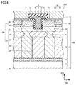
まず、第1実施形態に係る炭化珪素半導体装置200の構成について説明する。図1は、第1実施形態に係る炭化珪素半導体装置200の構成を示す断面模式図である。 (First Embodiment)
First, the configuration of the siliconcarbide semiconductor device 200 according to the first embodiment will be described. FIG. 1 is a schematic cross-sectional view showing the configuration of the silicon carbide semiconductor device 200 according to the first embodiment.
まず、第1実施形態に係る炭化珪素半導体装置200の構成について説明する。図1は、第1実施形態に係る炭化珪素半導体装置200の構成を示す断面模式図である。 (First Embodiment)
First, the configuration of the silicon
図1に示されるように、第1実施形態に係る炭化珪素半導体装置200は、トレンチ型MOSFETであり、炭化珪素基板100と、ゲート電極63と、ゲート絶縁膜51と、分離絶縁膜52と、第1電極61と、第2電極62とを主に有している。炭化珪素基板100は、第1主面1と、第1主面1と反対側の第2主面2とを有している。
As shown in FIG. 1, the silicon carbide semiconductor device 200 according to the first embodiment is a trench-type MOSFET, and includes a silicon carbide substrate 100, a gate electrode 63, a gate insulating film 51, a separation insulating film 52, and the like. It mainly has a first electrode 61 and a second electrode 62. The silicon carbide substrate 100 has a first main surface 1 and a second main surface 2 opposite to the first main surface 1.
第1主面1は、たとえば{0001}面または{0001}面に対して8°以下オフした面である。具体的には、第1主面1は、たとえば(000-1)面または(000-1)面に対して8°以下の角度で傾斜した面である。第1主面1は、たとえば(0001)面または(0001)面に対して8°以下の角度で傾斜した面であってもよい。
The first main surface 1 is, for example, a surface that is 8 ° or less off from the {0001} surface or the {0001} surface. Specifically, the first main surface 1 is, for example, a surface inclined at an angle of 8 ° or less with respect to the (000-1) surface or the (000-1) surface. The first main surface 1 may be, for example, a (0001) surface or a surface inclined at an angle of 8 ° or less with respect to the (0001) surface.
図1に示されるように、炭化珪素基板100は、第1不純物領域10と、第2不純物領域20と、第3不純物領域30とを含んでいる。第1不純物領域10は、たとえばN(窒素)などのn型を付与可能なn型不純物を含んでいる。第1不純物領域10は、たとえばn型(第1導電型)を有している。第1不純物領域10は、第2主面2の少なくとも一部を構成している。言い換えれば、第1不純物領域10は、第2主面2の全面を構成していてもよいし、第2主面2の一部を構成していてもよい。
As shown in FIG. 1, the silicon carbide substrate 100 includes a first impurity region 10, a second impurity region 20, and a third impurity region 30. The first impurity region 10 contains an n-type impurity that can impart an n-type such as N (nitrogen). The first impurity region 10 has, for example, an n-type (first conductive type). The first impurity region 10 constitutes at least a part of the second main surface 2. In other words, the first impurity region 10 may form the entire surface of the second main surface 2 or may form a part of the second main surface 2.
第1不純物領域10は、炭化珪素単結晶基板15と、バッファ層11と、第1スーパージャンクション領域12と、第1ジョイント領域13と、電流拡がり領域14とを有している。炭化珪素単結晶基板15は、第2主面2を構成している。炭化珪素単結晶基板15は、たとえばポリタイプ4Hの六方晶炭化珪素から構成されている。バッファ層11は、炭化珪素単結晶基板15上に設けられている。バッファ層11は、炭化珪素単結晶基板15に接している。
The first impurity region 10 has a silicon carbide single crystal substrate 15, a buffer layer 11, a first super junction region 12, a first joint region 13, and a current spreading region 14. The silicon carbide single crystal substrate 15 constitutes the second main surface 2. The silicon carbide single crystal substrate 15 is composed of, for example, a polytype 4H hexagonal silicon carbide. The buffer layer 11 is provided on the silicon carbide single crystal substrate 15. The buffer layer 11 is in contact with the silicon carbide single crystal substrate 15.
第1スーパージャンクション領域12は、バッファ層11上に設けられている。第1スーパージャンクション領域12は、バッファ層11に接している。第1方向101において、第1スーパージャンクション領域12の幅は、バッファ層11の幅よりも小さい。第3方向103における第1スーパージャンクション領域12の高さは、第1方向101における第1スーパージャンクション領域12の幅よりも大きくてもよい。第1スーパージャンクション領域12におけるn型不純物の濃度は、バッファ層11におけるn型不純物の濃度よりも低くてもよい。
The first super junction region 12 is provided on the buffer layer 11. The first super junction region 12 is in contact with the buffer layer 11. In the first direction 101, the width of the first super junction region 12 is smaller than the width of the buffer layer 11. The height of the first super junction region 12 in the third direction 103 may be larger than the width of the first super junction region 12 in the first direction 101. The concentration of the n-type impurity in the first super junction region 12 may be lower than the concentration of the n-type impurity in the buffer layer 11.
第1ジョイント領域13は、第1スーパージャンクション領域12上に設けられている。第1ジョイント領域13は、第1スーパージャンクション領域12に接している。第1ジョイント領域13は、中央の幅が上下の各々の幅よりも小さくなるように狭窄していてもよい。電流拡がり領域14は、第1ジョイント領域13上に設けられている。電流拡がり領域14は、第1ジョイント領域13に接している。電流拡がり領域14は、トレンチ5の底面4および側面3の各々に接している。
The first joint region 13 is provided on the first super junction region 12. The first joint region 13 is in contact with the first super junction region 12. The first joint region 13 may be narrowed so that the central width is smaller than the upper and lower widths. The current spreading region 14 is provided on the first joint region 13. The current spreading region 14 is in contact with the first joint region 13. The current spreading region 14 is in contact with each of the bottom surface 4 and the side surface 3 of the trench 5.
第1不純物領域10の不純物濃度は、たとえば6×1016cm-3以上である。具体的には、第1不純物領域10の第1スーパージャンクション領域12のn型不純物の濃度は、たとえば6×1016cm-3以上である。第1不純物領域10の第1スーパージャンクション領域12のn型不純物の濃度は、たとえば8×1016cm-3以上であってもよいし、10×1016cm-3以上であってもよい。
The impurity concentration of the first impurity region 10 is, for example, 6 × 10 16 cm -3 or more. Specifically, the concentration of the n-type impurity in the first super junction region 12 of the first impurity region 10 is, for example, 6 × 10 16 cm -3 or more. The concentration of the n-type impurity in the first super junction region 12 of the first impurity region 10 may be, for example, 8 × 10 16 cm -3 or more, or 10 × 10 16 cm -3 or more.
第1不純物領域10の第1ジョイント領域13のn型不純物の濃度は、たとえば6×1016cm-3以上である。第1不純物領域10の電流拡がり領域14のn型不純物の濃度は、たとえば6×1016cm-3以上である。第1スーパージャンクション領域12、第1ジョイント領域13および電流拡がり領域14の各々のn型不純物の濃度は、たとえば6×1016cm-3以上であってもよい。
The concentration of the n-type impurity in the first joint region 13 of the first impurity region 10 is, for example, 6 × 10 16 cm -3 or more. The concentration of the n-type impurity in the current spreading region 14 of the first impurity region 10 is, for example, 6 × 10 16 cm -3 or more. The concentration of each of the n-type impurities in the first super junction region 12, the first joint region 13, and the current spreading region 14 may be, for example, 6 × 10 16 cm -3 or more.
第2不純物領域20は、たとえばAl(アルミニウム)などのp型を付与可能なp型不純物を含んでいる。第2不純物領域20は、n型と異なるp型(第2導電型)を有している。第2不純物領域20は、第1不純物領域10に接して設けられている。第2不純物領域20と第1不純物領域10とはPNダイオードを構成する。第2不純物領域20は、第1主面1の少なくとも一部を構成している。言い換えれば、第2不純物領域20は、第1主面1の全面を構成していてもよいし、第1主面1の一部を構成していてもよい。
The second impurity region 20 contains a p-type impurity such as Al (aluminum) that can be imparted with a p-type. The second impurity region 20 has a p-type (second conductive type) different from the n-type. The second impurity region 20 is provided in contact with the first impurity region 10. The second impurity region 20 and the first impurity region 10 form a PN diode. The second impurity region 20 constitutes at least a part of the first main surface 1. In other words, the second impurity region 20 may form the entire surface of the first main surface 1 or may form a part of the first main surface 1.
第2不純物領域20は、第1領域21と、第2領域22とを有している。第2領域22は、第1領域21と第2主面2との間にある。第2領域22は、第1領域21に接している。第1領域21は、第1主面1の少なくとも一部を構成している。第1領域21は、たとえば、第1部分41と、第2部分42とを有していてもよい。第1部分41は、第2部分42上にある。第2部分42は、第1部分41に接している。第1部分41におけるp型不純物の濃度は、第2部分42におけるp型不純物の濃度よりも高くてもよい。第2部分42は、たとえばチャネル層である。第1領域21は、第1部分41を有していなくてもよい。第2領域22は、バッファ層11に接していてもよい。
The second impurity region 20 has a first region 21 and a second region 22. The second region 22 is between the first region 21 and the second main surface 2. The second region 22 is in contact with the first region 21. The first region 21 constitutes at least a part of the first main surface 1. The first region 21 may have, for example, a first portion 41 and a second portion 42. The first portion 41 is on the second portion 42. The second portion 42 is in contact with the first portion 41. The concentration of the p-type impurity in the first portion 41 may be higher than the concentration of the p-type impurity in the second portion 42. The second part 42 is, for example, a channel layer. The first region 21 does not have to have the first portion 41. The second region 22 may be in contact with the buffer layer 11.
第2領域22は、第2スーパージャンクション領域25と、第2ジョイント領域24と、第3ジョイント領域23とを有している。第2スーパージャンクション領域25は、バッファ層11上に設けられている。第2スーパージャンクション領域25は、バッファ層11に接している。第1方向101において、第2スーパージャンクション領域25の幅は、バッファ層11の幅よりも小さい。第3方向103における第2スーパージャンクション領域25の高さは、第1方向101における第2スーパージャンクション領域25の幅よりも大きくてもよい。
The second region 22 has a second super junction region 25, a second joint region 24, and a third joint region 23. The second super junction region 25 is provided on the buffer layer 11. The second super junction region 25 is in contact with the buffer layer 11. In the first direction 101, the width of the second super junction region 25 is smaller than the width of the buffer layer 11. The height of the second super junction region 25 in the third direction 103 may be larger than the width of the second super junction region 25 in the first direction 101.
第1スーパージャンクション領域12と第2スーパージャンクション領域25とは、スーパージャンクションを構成する。第1スーパージャンクション領域12は、第2スーパージャンクション領域25に接している。第1方向101において、第1スーパージャンクション領域12と第2スーパージャンクション領域25とは、交互に配置されている。第2スーパージャンクション領域25におけるp型不純物の濃度は、第1スーパージャンクション領域12におけるn型不純物の濃度と同程度であってもよい。第1方向101において、第2スーパージャンクション領域25の幅は、第1スーパージャンクション領域12の幅と同程度であってもよい。
The first super junction area 12 and the second super junction area 25 form a super junction. The first super junction region 12 is in contact with the second super junction region 25. In the first direction 101, the first super junction region 12 and the second super junction region 25 are arranged alternately. The concentration of p-type impurities in the second super-junction region 25 may be about the same as the concentration of n-type impurities in the first super-junction region 12. In the first direction 101, the width of the second super junction region 25 may be about the same as the width of the first super junction region 12.
第2ジョイント領域24は、第2スーパージャンクション領域25上に設けられている。第2ジョイント領域24は、第2スーパージャンクション領域25に接している。第2ジョイント領域24は、中央の幅が上下の各々の幅よりも大きくなるように拡張していてもよい。第1方向101において、第2ジョイント領域24の最大幅は、第2スーパージャンクション領域25の幅よりも大きくてもよい。第2ジョイント領域24は、第1ジョイント領域13に接している。第1方向101において、第2ジョイント領域24と、第1ジョイント領域13とは、交互に配置されている。
The second joint region 24 is provided on the second super junction region 25. The second joint region 24 is in contact with the second super junction region 25. The second joint region 24 may be extended so that the width at the center is larger than the width of each of the upper and lower parts. In the first direction 101, the maximum width of the second joint region 24 may be larger than the width of the second super junction region 25. The second joint region 24 is in contact with the first joint region 13. In the first direction 101, the second joint region 24 and the first joint region 13 are arranged alternately.
第3ジョイント領域23は、第2ジョイント領域24上に設けられている。第3ジョイント領域23は、第2ジョイント領域24および第1領域21の各々に接している。第3方向103において、第3ジョイント領域23は、第2ジョイント領域24と第1領域21との間に位置している。第1方向101において、第3ジョイント領域23は、電流拡がり領域14に接している。
The third joint region 23 is provided on the second joint region 24. The third joint region 23 is in contact with each of the second joint region 24 and the first region 21. In the third direction 103, the third joint region 23 is located between the second joint region 24 and the first region 21. In the first direction 101, the third joint region 23 is in contact with the current spreading region 14.
第2領域22の不純物濃度は、6×1016cm-3以上である。具体的には、第2領域22の第2スーパージャンクション領域25のp型不純物の濃度は、6×1016cm-3以上である。第2領域22の第2スーパージャンクション領域25のp型不純物の濃度は、8×1016cm-3以上であってもよいし、10×1016cm-3以上であってもよい。第2領域22の第2スーパージャンクション領域25のp型不純物の濃度の上限は、特に限定されないが、たとえば6×1018cm-3以下であってもよい。
The impurity concentration of the second region 22 is 6 × 10 16 cm -3 or more. Specifically, the concentration of p-type impurities in the second superjunction region 25 of the second region 22 is 6 × 10 16 cm -3 or more. The concentration of the p-type impurity in the second superjunction region 25 of the second region 22 may be 8 × 10 16 cm -3 or more, or 10 × 10 16 cm -3 or more. The upper limit of the concentration of the p-type impurity in the second superjunction region 25 of the second region 22 is not particularly limited, but may be , for example, 6 × 10 18 cm -3 or less.
第2領域22の第2ジョイント領域24のp型不純物の濃度は、たとえば6×1016cm-3以上である。第2領域22の第3ジョイント領域23のp型不純物の濃度は、たとえば6×1016cm-3以上である。第2スーパージャンクション領域25、第2ジョイント領域24および第3ジョイント領域23の各々のp型不純物の濃度は、たとえば6×1016cm-3以上であってもよい。
The concentration of p-type impurities in the second joint region 24 of the second region 22 is, for example, 6 × 10 16 cm -3 or more. The concentration of p-type impurities in the third joint region 23 of the second region 22 is, for example, 6 × 10 16 cm -3 or more. The concentration of each p-type impurity in the second superjunction region 25, the second joint region 24, and the third joint region 23 may be, for example, 6 × 10 16 cm -3 or more.
第3不純物領域30は、第1不純物領域10から隔てられるように第2不純物領域20に接して設けられている。第3不純物領域30は、たとえばP(リン)などのn型を付与可能なn型不純物を含んでいる。第3不純物領域30は、たとえばn型を有している。第3不純物領域30は、たとえばソース領域である。第3不純物領域30は、第1主面1の一部を構成していてもよい。第3不純物領域30が含むn型不純物の濃度は、第2部分42が含むp型不純物の濃度よりも高くてもよい。
The third impurity region 30 is provided in contact with the second impurity region 20 so as to be separated from the first impurity region 10. The third impurity region 30 contains an n-type impurity that can impart an n-type such as P (phosphorus). The third impurity region 30 has, for example, an n-type. The third impurity region 30 is, for example, a source region. The third impurity region 30 may form a part of the first main surface 1. The concentration of the n-type impurity contained in the third impurity region 30 may be higher than the concentration of the p-type impurity contained in the second portion 42.
第1領域21の不純物濃度は、6×1016cm-3以上である。具体的には、第1領域21のp型不純物の濃度は、6×1016cm-3以上である。第1領域21の不純物濃度は、第2領域22の不純物濃度よりも高くてもよい。具体的には、第1領域21の第2部分42のp型不純物の濃度は、第2領域22のp型不純物の濃度よりも高くてもよい。第1領域21の不純物濃度は、1×1019cm-3以下であってもよい。具体的には、第1領域21の第2部分42のp型不純物の濃度は、1×1019cm-3以下であってもよい。第1領域21の第2部分42のp型不純物の濃度は、8×1018cm-3以下であってもよいし、6×1018cm-3以下であってもよい。第1領域21の第2部分42のp型不純物の濃度の下限は、特に限定されないが、たとえば6×1017cm-3以上であってもよい。
The impurity concentration of the first region 21 is 6 × 10 16 cm -3 or more. Specifically, the concentration of p-type impurities in the first region 21 is 6 × 10 16 cm -3 or more. The impurity concentration of the first region 21 may be higher than the impurity concentration of the second region 22. Specifically, the concentration of the p-type impurity in the second portion 42 of the first region 21 may be higher than the concentration of the p-type impurity in the second region 22. The impurity concentration of the first region 21 may be 1 × 10 19 cm -3 or less. Specifically, the concentration of the p-type impurity in the second portion 42 of the first region 21 may be 1 × 10 19 cm -3 or less. The concentration of the p-type impurity in the second portion 42 of the first region 21 may be 8 × 10 18 cm -3 or less, or 6 × 10 18 cm -3 or less. The lower limit of the concentration of the p-type impurity in the second portion 42 of the first region 21 is not particularly limited, but may be , for example, 6 × 10 17 cm -3 or more.
炭化珪素基板100には、トレンチ5が設けられている。トレンチ5は、第1主面1に開口している。トレンチ5は、側面3と、底面4とを有している。底面4は、側面3に連なっている。側面3は、第1不純物領域10、第2不純物領域20および第3不純物領域30の各々と接している。具体的には、側面3は、電流拡がり領域14、第2部分42および第3不純物領域30の各々と接している。底面4は、第1不純物領域10に接している。具体的には、底面4は、電流拡がり領域14に接している。
The silicon carbide substrate 100 is provided with a trench 5. The trench 5 is open to the first main surface 1. The trench 5 has a side surface 3 and a bottom surface 4. The bottom surface 4 is connected to the side surface 3. The side surface 3 is in contact with each of the first impurity region 10, the second impurity region 20, and the third impurity region 30. Specifically, the side surface 3 is in contact with each of the current spreading region 14, the second portion 42, and the third impurity region 30. The bottom surface 4 is in contact with the first impurity region 10. Specifically, the bottom surface 4 is in contact with the current spreading region 14.
第1主面1に垂直な断面において、トレンチ5の形状は、V型であってもよい。トレンチ5の形状がV型であるとは、トレンチ5の側面3と第1主面1とがなす角度θが、90°より大きく180°未満であることである。角度θは、たとえば115°以上135°以下であってもよい。
In the cross section perpendicular to the first main surface 1, the shape of the trench 5 may be V-shaped. The V-shaped shape of the trench 5 means that the angle θ formed by the side surface 3 of the trench 5 and the first main surface 1 is larger than 90 ° and less than 180 °. The angle θ may be, for example, 115 ° or more and 135 ° or less.
ゲート絶縁膜51は、たとえば二酸化珪素から構成されている。ゲート絶縁膜51は、トレンチ5の内部に配置されている。ゲート絶縁膜51は、トレンチ5の側面3において、第1不純物領域10、第2不純物領域20および第3不純物領域30の各々に接している。ゲート絶縁膜51は、トレンチ5の底面4において、電流拡がり領域14に接している。ゲート絶縁膜51に接する第2不純物領域20の第2部分42には、チャネルが形成可能に構成されている。ゲート絶縁膜51は、第1主面1において、第3不純物領域30に接している。ゲート絶縁膜51の厚みは、たとえば40nm以上150nm以下である。
The gate insulating film 51 is made of, for example, silicon dioxide. The gate insulating film 51 is arranged inside the trench 5. The gate insulating film 51 is in contact with each of the first impurity region 10, the second impurity region 20, and the third impurity region 30 on the side surface 3 of the trench 5. The gate insulating film 51 is in contact with the current spreading region 14 on the bottom surface 4 of the trench 5. A channel can be formed in the second portion 42 of the second impurity region 20 in contact with the gate insulating film 51. The gate insulating film 51 is in contact with the third impurity region 30 on the first main surface 1. The thickness of the gate insulating film 51 is, for example, 40 nm or more and 150 nm or less.
ゲート電極63は、ゲート絶縁膜51上に設けられている。ゲート絶縁膜51に接触して配置されている。ゲート電極63の少なくとも一部は、トレンチ5の内部に配置されている。ゲート電極63は、たとえば不純物がドーピングされたポリシリコンなどの導電体から構成されている。
The gate electrode 63 is provided on the gate insulating film 51. It is arranged in contact with the gate insulating film 51. At least a part of the gate electrode 63 is arranged inside the trench 5. The gate electrode 63 is composed of a conductor such as polysilicon doped with impurities, for example.
分離絶縁膜52は、ゲート電極63を覆うように設けられている。分離絶縁膜52は、ゲート電極63およびゲート絶縁膜51の各々に接している。分離絶縁膜52は、たとえばNSG(None-doped Silicate Glass)膜またはPSG(Phosphorus Silicate Glass)膜などにより構成されている。分離絶縁膜52は、ゲート電極63と第1電極61とを電気的に絶縁している。
The separation insulating film 52 is provided so as to cover the gate electrode 63. The separation insulating film 52 is in contact with each of the gate electrode 63 and the gate insulating film 51. The separation insulating film 52 is composed of, for example, an NSG (None-topped Silicate Glass) film or a PSG (Phosphorus Silicate Glass) film. The separation insulating film 52 electrically insulates the gate electrode 63 and the first electrode 61.
第1電極61は、第1主面1に設けられている。第1電極61は、たとえばソース電極である。第1電極61は、電極層60と、配線層64とを有している。電極層60は、たとえばTi(チタン)とAl(アルミニウム)とSi(シリコン)を含む材料から構成されている。電極層60はNi(ニッケル)を含んでもよい。配線層64は、たとえばAlを含む材料から構成されている。
The first electrode 61 is provided on the first main surface 1. The first electrode 61 is, for example, a source electrode. The first electrode 61 has an electrode layer 60 and a wiring layer 64. The electrode layer 60 is made of a material containing, for example, Ti (titanium), Al (aluminum), and Si (silicon). The electrode layer 60 may contain Ni (nickel). The wiring layer 64 is made of, for example, a material containing Al.
第1電極61は、第1主面1において、第2不純物領域20および第3不純物領域30の各々に接している。具体的には、電極層60は、第1主面1において、第1部分41および第3不純物領域30の各々に接している。第1電極61は、トレンチ5を跨ぐように配置されていてもよい。第1電極61は、分離絶縁膜52を覆っていてもよい。第1電極61は、第2不純物領域20と電気的に接続されている。第1電極61は、第3不純物領域30と電気的に接続されている。第1不純物領域10がn型でありかつ第2不純物領域20がp型である場合、第1電極61はアノード電極として機能する。
The first electrode 61 is in contact with each of the second impurity region 20 and the third impurity region 30 on the first main surface 1. Specifically, the electrode layer 60 is in contact with each of the first portion 41 and the third impurity region 30 on the first main surface 1. The first electrode 61 may be arranged so as to straddle the trench 5. The first electrode 61 may cover the separation insulating film 52. The first electrode 61 is electrically connected to the second impurity region 20. The first electrode 61 is electrically connected to the third impurity region 30. When the first impurity region 10 is n-type and the second impurity region 20 is p-type, the first electrode 61 functions as an anode electrode.
第2電極62は、第2主面2に設けられている。第2電極62は、たとえばドレイン電極である。第2電極62は、第2主面2において、第1不純物領域10に接している。具体的には、第2電極62は、第2主面2において、炭化珪素単結晶基板15に接している。第2電極62は、第1不純物領域10と電気的に接続されている。第1不純物領域10がn型でありかつ第2不純物領域20がp型である場合、第2電極62はカソード電極として機能する。第2電極62は、たとえばNiSi(ニッケルシリサイド)など、n型の炭化珪素単結晶基板15とオーミック接合可能な材料から構成されている。
The second electrode 62 is provided on the second main surface 2. The second electrode 62 is, for example, a drain electrode. The second electrode 62 is in contact with the first impurity region 10 on the second main surface 2. Specifically, the second electrode 62 is in contact with the silicon carbide single crystal substrate 15 on the second main surface 2. The second electrode 62 is electrically connected to the first impurity region 10. When the first impurity region 10 is n-type and the second impurity region 20 is p-type, the second electrode 62 functions as a cathode electrode. The second electrode 62 is made of a material that can be ohmic-bonded to the n-type silicon carbide single crystal substrate 15, such as NiSi (nickel silicide).
なお、第1実施形態に係る炭化珪素半導体装置200においては、逆方向特性における耐圧は、たとえば600V以上であり、好ましくは1100V以上である。
In the silicon carbide semiconductor device 200 according to the first embodiment, the withstand voltage in the reverse direction characteristic is, for example, 600 V or more, preferably 1100 V or more.
次に、各不純物領域におけるp型不純物の濃度およびn型不純物の濃度の測定方法について説明する。
Next, a method for measuring the concentration of p-type impurities and the concentration of n-type impurities in each impurity region will be described.
各不純物領域におけるp型不純物の濃度およびn型不純物の濃度は、SIMS(Secondary Ion Mass Spectrometry)を用いて測定することができる。測定装置は、たとえばCameca製の二次イオン質量分析装置である。測定ピッチは、たとえば0.01μmである。検出するn型不純物が窒素の場合、一次イオンビーム(primary ion beam)は、セシウム(Cs)である。一次イオンエネルギーは、14.5keVである。二次イオンの極性(secondary ion polarity)は、負(negative)である。検出するp型不純物がアルミニウムまたはホウ素の場合、一次イオンビーム(primary ion beam)は、酸素(O2)である。一次イオンエネルギーは、8keVである。二次イオンの極性(secondary ion polarity)は、正(positive)である。
The concentration of p-type impurities and the concentration of n-type impurities in each impurity region can be measured using SIMS (Seconday Ion Mass Spectrometry). The measuring device is, for example, a secondary ion mass spectrometer manufactured by Cameca. The measurement pitch is, for example, 0.01 μm. When the n-type impurity to be detected is nitrogen, the primary ion beam is cesium (Cs). The primary ion energy is 14.5 keV. The polarity of the secondary ion is negative. When the p-type impurity to be detected is aluminum or boron, the primary ion beam is oxygen (O 2 ). The primary ion energy is 8 keV. The polarity of the secondary ion is positive.
次に、p型領域とn型領域との判別方法について説明する。
p型領域とn型領域との判別方法には、SCM(Scanning Capacitance Microscope)が用いられる。測定装置は、たとえばブルカー・エイエックスエス社製のNanoScope IVである。SCMは、半導体中のキャリア濃度分布を可視化する方法である。具体的には、金属コートされたシリコン探針を用いて、試料の表面上が走査される。その際、試料に高周波電圧が印加される。多数キャリアを励振して系の静電容量に変調が加えられる。試料に印可される高周波電圧の周波数は、100kHzであり、電圧は4.0Vである。 Next, a method of discriminating between the p-type region and the n-type region will be described.
SCM (Scanning Capacitance Microscope) is used as a method for discriminating between the p-type region and the n-type region. The measuring device is, for example, the NanoScope IV manufactured by Bruker AXS. SCM is a method of visualizing the carrier concentration distribution in a semiconductor. Specifically, a metal-coated silicon probe is used to scan the surface of the sample. At that time, a high frequency voltage is applied to the sample. Modulation is applied to the capacitance of the system by exciting a large number of carriers. The frequency of the high frequency voltage applied to the sample is 100 kHz and the voltage is 4.0 V.
図2は、図1のII-II線に沿った断面模式図である。図2に示されるように、第2主面2に垂直な方向に見て、第2スーパージャンクション領域25は、たとえば第2方向102に沿って延在している。別の観点から言えば、第2スーパージャンクション領域25の長手方向は、たとえば第2方向102である。第2スーパージャンクション領域25の短手方向は、たとえば第1方向101である。第2主面2に垂直な方向に見て、第2スーパージャンクション領域25は、実質的に長方形状であってもよい。第2主面2に垂直な方向に見て、第1スーパージャンクション領域12は、第2スーパージャンクション領域25を取り囲んでいてもよい。
FIG. 2 is a schematic cross-sectional view taken along the line II-II of FIG. As shown in FIG. 2, the second superjunction region 25 extends along, for example, the second direction 102 when viewed in a direction perpendicular to the second main surface 2. From another point of view, the longitudinal direction of the second super junction region 25 is, for example, the second direction 102. The lateral direction of the second super junction region 25 is, for example, the first direction 101. The second superjunction region 25 may be substantially rectangular when viewed in a direction perpendicular to the second main surface 2. The first super-junction region 12 may surround the second super-junction region 25 when viewed in a direction perpendicular to the second main surface 2.
第1方向101および第2方向102の各々は、第2主面2に平行である。第3方向103は、第2主面2に対して垂直である。第1方向101は、たとえば<11-20>方向である。第2方向102は、たとえば<1-100>方向である。第3方向103は、たとえば<0001>方向である。第1方向101は、たとえば<11-20>方向を第1主面1に射影した方向であってもよい。第2方向102は、たとえば<1-100>方向を第1主面1に射影した方向であってもよい。第3方向103は、たとえば<0001>方向に対して傾斜した方向であってもよい。
Each of the first direction 101 and the second direction 102 is parallel to the second main surface 2. The third direction 103 is perpendicular to the second main surface 2. The first direction 101 is, for example, the <11-20> direction. The second direction 102 is, for example, the <1-100> direction. The third direction 103 is, for example, the <0001> direction. The first direction 101 may be, for example, a direction in which the <11-20> direction is projected onto the first main surface 1. The second direction 102 may be, for example, a direction in which the <1-100> direction is projected onto the first main surface 1. The third direction 103 may be, for example, a direction inclined with respect to the <0001> direction.
図3は、図2の領域IIIの拡大模式図である。図3に示されるように、第2領域22は、点欠陥9を有している。点欠陥9のエネルギー準位は、Ec(伝導帯の底のエネルギー)より0.5eV以上深く、Ev(価電子帯の頂上のエネルギー)より0.4eV以上高い。点欠陥9は、Z1/2センターと呼ばれる第1欠陥7と、EH6/7センターと呼ばれる第2欠陥8とを有していてもよい。Z1/2センターのエネルギー準位は、Ec(伝導帯の底のエネルギー)-0.65eVである。EH6/7センターのエネルギー準位は、Ec(伝導帯の底のエネルギー)-1.55eVである。第2領域22は、第1欠陥7および第2欠陥8の双方を有していてもよいし、第1欠陥7のみを有していてもよいし、第2欠陥8のみを有していてもよい。
FIG. 3 is an enlarged schematic view of region III of FIG. As shown in FIG. 3, the second region 22 has a point defect 9. The energy level of the point defect 9 is 0.5 eV or more deeper than Ec (the energy at the bottom of the conduction band) and 0.4 eV or more higher than Ev (the energy at the top of the valence band). The point defect 9 may have a first defect 7 called a Z 1/2 center and a second defect 8 called an EH 6/7 center. The energy level of the Z 1/2 center is Ec (the energy at the bottom of the conduction band) -0.65 eV. The energy level of the EH 6/7 center is Ec (the energy at the bottom of the conduction band) -1.55 eV. The second region 22 may have both the first defect 7 and the second defect 8, may have only the first defect 7, or may have only the second defect 8. May be good.
第2領域22の点欠陥密度は、6×1012cm-3以上である。第2領域22の点欠陥密度は、たとえば8×1012cm-3以上であってもよいし、10×1012cm-3以上であってもよい。第2領域22の点欠陥密度は、たとえば1×1014cm-3以下であってもよい。第2領域22の点欠陥密度は、たとえば0.8×1014cm-3以下であってもよいし、0.6×1014cm-3以下であってもよい。なお、第2領域22が第1欠陥7と第2欠陥8とを有している場合には、第2領域22の点欠陥密度とは、第1欠陥7および第2欠陥8の合計の点欠陥密度である。
The point defect density of the second region 22 is 6 × 10 12 cm -3 or more. The point defect density of the second region 22 may be, for example, 8 × 10 12 cm -3 or more, or 10 × 10 12 cm -3 or more. The point defect density of the second region 22 may be, for example, 1 × 10 14 cm -3 or less. The point defect density of the second region 22 may be, for example, 0.8 × 10 14 cm -3 or less, or 0.6 × 10 14 cm -3 or less. When the second region 22 has the first defect 7 and the second defect 8, the point defect density of the second region 22 is the total point of the first defect 7 and the second defect 8. Defect density.
次に、点欠陥密度の測定方法について説明する。
点欠陥密度は、DLTS(Deep Level Transient Spectroscopy)法および/またはICTS法(Isothermal Capacitance Transient Spectroscopy)によって測定することができる。DLTS法においては、パルス幅を一定にして温度を変えて、接合容量の時間変化が得られる。ICTS法においては、温度を一定にしてパルス幅を変えて、接合容量の時間変化が得られる。DLTS法およびICTS法のいずれか一方の方法で点欠陥の情報が得られるが、双方を行うことで、点欠陥の情報がより正確に得られる。測定装置としては、たとえばPhystech社製FT1230を使用することができる。試料の温度は77K~773Kの範囲であり、パルス電圧を印加して接合容量の時間変化を得る。パルスは+20V~-20Vの電圧を使い、1μs~60sのパルス幅を使う。接合容量の過渡変化をフーリエ変換やラプラス変換して、点欠陥密度とそのエネルギー準位を得ることができる。 Next, a method for measuring the point defect density will be described.
The point defect density can be measured by the DLTS (Deep Level Transient Spectroscopy) method and / or the ICTS method (Isothermal Capacitance Spectroscopy). In the DLTS method, the pulse width is kept constant and the temperature is changed to obtain a time change of the junction capacitance. In the ICTS method, the temperature is kept constant and the pulse width is changed to obtain a time change of the junction capacitance. The point defect information can be obtained by either the DLTS method or the ICTS method, but by performing both methods, the point defect information can be obtained more accurately. As the measuring device, for example, FT1230 manufactured by Moskovskiy can be used. The temperature of the sample is in the range of 77K to 773K, and a pulse voltage is applied to obtain a time change of the junction capacitance. The pulse uses a voltage of + 20V to -20V and a pulse width of 1μs to 60s. The point defect density and its energy level can be obtained by Fourier transform or Laplace transform of the transient change of the junction capacitance.
(第2実施形態)
次に、第2実施形態に係る炭化珪素半導体装置200の構成について説明する。第2実施形態に係る炭化珪素半導体装置200は、トレンチ5の形状がU型である構成において、第1実施形態に係る炭化珪素半導体装置200と異なっており、その他の構成については、第1実施形態に係る炭化珪素半導体装置200と同様である。以下、第1実施形態に係る炭化珪素半導体装置200と異なる構成を中心に説明する。 (Second Embodiment)
Next, the configuration of the siliconcarbide semiconductor device 200 according to the second embodiment will be described. The silicon carbide semiconductor device 200 according to the second embodiment is different from the silicon carbide semiconductor device 200 according to the first embodiment in the configuration in which the shape of the trench 5 is U-shaped, and the other configurations are the first embodiment. This is the same as the silicon carbide semiconductor device 200 according to the embodiment. Hereinafter, a configuration different from that of the silicon carbide semiconductor device 200 according to the first embodiment will be mainly described.
次に、第2実施形態に係る炭化珪素半導体装置200の構成について説明する。第2実施形態に係る炭化珪素半導体装置200は、トレンチ5の形状がU型である構成において、第1実施形態に係る炭化珪素半導体装置200と異なっており、その他の構成については、第1実施形態に係る炭化珪素半導体装置200と同様である。以下、第1実施形態に係る炭化珪素半導体装置200と異なる構成を中心に説明する。 (Second Embodiment)
Next, the configuration of the silicon
図4は、第2実施形態に係る炭化珪素半導体装置200の構成を示す断面模式図である。図4に示されるように、第1主面1に垂直な断面において、トレンチ5の形状は、U型である。具体的には、トレンチ5は、側面3と、底面4とを有している。第1主面1と側面3とがなす角度θは、90°である。側面3は、第1主面1に対してほぼ垂直に延在している。底面4は、第1主面1にほぼ平行に延在している。側面3と底面4との境界は、丸まっていてもよい。
FIG. 4 is a schematic cross-sectional view showing the configuration of the silicon carbide semiconductor device 200 according to the second embodiment. As shown in FIG. 4, the shape of the trench 5 is U-shaped in the cross section perpendicular to the first main surface 1. Specifically, the trench 5 has a side surface 3 and a bottom surface 4. The angle θ formed by the first main surface 1 and the side surface 3 is 90 °. The side surface 3 extends substantially perpendicular to the first main surface 1. The bottom surface 4 extends substantially parallel to the first main surface 1. The boundary between the side surface 3 and the bottom surface 4 may be rounded.
(第3実施形態)
次に、第3実施形態に係る炭化珪素半導体装置200の構成について説明する。第3実施形態に係る炭化珪素半導体装置200は、プレナー型である構成において、第1実施形態に係る炭化珪素半導体装置200と異なっており、その他の構成については、第1実施形態に係る炭化珪素半導体装置200と同様である。以下、第1実施形態に係る炭化珪素半導体装置200と異なる構成を中心に説明する。 (Third Embodiment)
Next, the configuration of the siliconcarbide semiconductor device 200 according to the third embodiment will be described. The silicon carbide semiconductor device 200 according to the third embodiment is different from the silicon carbide semiconductor device 200 according to the first embodiment in a planar type configuration, and the silicon carbide semiconductor device 200 according to the first embodiment is different from the silicon carbide semiconductor device 200 according to the first embodiment. It is the same as the semiconductor device 200. Hereinafter, a configuration different from that of the silicon carbide semiconductor device 200 according to the first embodiment will be mainly described.
次に、第3実施形態に係る炭化珪素半導体装置200の構成について説明する。第3実施形態に係る炭化珪素半導体装置200は、プレナー型である構成において、第1実施形態に係る炭化珪素半導体装置200と異なっており、その他の構成については、第1実施形態に係る炭化珪素半導体装置200と同様である。以下、第1実施形態に係る炭化珪素半導体装置200と異なる構成を中心に説明する。 (Third Embodiment)
Next, the configuration of the silicon
図5は、第3実施形態に係る炭化珪素半導体装置200の構成を示す断面模式図である。図5に示されるように、第3実施形態に係る炭化珪素半導体装置200は、プレナー型である。ゲート絶縁膜51は、第1主面1上に設けられている。ゲート絶縁膜51は、第1主面1において、第3不純物領域30、第2部分42および電流拡がり領域14の各々に接していてもよい。第2部分42は、第1主面1の一部を構成していてもよい。電流拡がり領域14は、第1主面1の一部を構成していてもよい。ゲート電極63は、第3不純物領域30、第2部分42および電流拡がり領域14の各々に対向していてもよい。
FIG. 5 is a schematic cross-sectional view showing the configuration of the silicon carbide semiconductor device 200 according to the third embodiment. As shown in FIG. 5, the silicon carbide semiconductor device 200 according to the third embodiment is a planar type. The gate insulating film 51 is provided on the first main surface 1. The gate insulating film 51 may be in contact with each of the third impurity region 30, the second portion 42, and the current spreading region 14 on the first main surface 1. The second portion 42 may form a part of the first main surface 1. The current spreading region 14 may form a part of the first main surface 1. The gate electrode 63 may face each of the third impurity region 30, the second portion 42, and the current spreading region 14.
(炭化珪素半導体装置の製造方法)
次に、本実施形態に係る炭化珪素半導体装置の製造方法について説明する。 (Manufacturing method of silicon carbide semiconductor device)
Next, a method for manufacturing the silicon carbide semiconductor device according to the present embodiment will be described.
次に、本実施形態に係る炭化珪素半導体装置の製造方法について説明する。 (Manufacturing method of silicon carbide semiconductor device)
Next, a method for manufacturing the silicon carbide semiconductor device according to the present embodiment will be described.
図6に示されるように、本実施形態に係る炭化珪素半導体装置200の製造方法は、炭化珪素基板を準備する工程(S10:図6)と、第1電極を形成する工程(S20:図6)と、第2電極を形成する工程(S30:図6)とを主に有している。図7に示されるように、炭化珪素基板を準備する工程(S10:図6)は、炭化珪素単結晶基板を準備する工程(S11:図7)と、第2領域を形成する工程(S12:図7)と、活性化アニール工程(S13:図7)とを主に有している。
As shown in FIG. 6, the method for manufacturing the silicon carbide semiconductor device 200 according to the present embodiment includes a step of preparing a silicon carbide substrate (S10: FIG. 6) and a step of forming a first electrode (S20: FIG. 6). ) And a step of forming the second electrode (S30: FIG. 6). As shown in FIG. 7, the steps of preparing the silicon carbide substrate (S10: FIG. 6) include the step of preparing the silicon carbide single crystal substrate (S11: FIG. 7) and the step of forming the second region (S12: FIG. It mainly has FIG. 7) and an activation annealing step (S13: FIG. 7).
まず、炭化珪素単結晶基板を準備する工程(S11:図7)が実施される。たとえば昇華法によって製造された炭化珪素インゴット(図示せず)がスライスされることにより、炭化珪素単結晶基板15が準備される。図8に示されるように、炭化珪素単結晶基板15は、第3主面6と、第2主面2とを有している。第2主面2は、第3主面6の反対側にある。炭化珪素単結晶基板15を構成する炭化珪素のポリタイプは、たとえば4Hである。ポリタイプは、6Hであってもよいし、15Rであってもよいし、3Cであってもよい。6Hは、六方晶である。15Hは、菱面体晶である。3Cは、立方晶である。
First, a step of preparing a silicon carbide single crystal substrate (S11: FIG. 7) is carried out. For example, a silicon carbide single crystal substrate 15 is prepared by slicing a silicon carbide ingot (not shown) produced by a sublimation method. As shown in FIG. 8, the silicon carbide single crystal substrate 15 has a third main surface 6 and a second main surface 2. The second main surface 2 is on the opposite side of the third main surface 6. The polytype of silicon carbide constituting the silicon carbide single crystal substrate 15 is, for example, 4H. The polytype may be 6H, 15R, or 3C. 6H is a hexagonal crystal. 15H is a rhombohedral crystal. 3C is a cubic crystal.
次に、バッファ層11が形成される。たとえば原料ガスとしてシラン(SiH4)とプロパン(C3H8)との混合ガスを用い、キャリアガスとしてたとえば水素(H2)を用いたCVD(Chemical Vapor Deposition)法により、炭化珪素単結晶基板15上にバッファ層11が形成される(図9参照)。エピタキシャル成長の際、たとえば窒素などのn型不純物がバッファ層11に導入される。
Next, the buffer layer 11 is formed. For example, a silicon carbide single crystal substrate by the CVD (Chemical Vapor Deposition) method using a mixed gas of silane (SiH 4 ) and propane (C 3 H 8 ) as a raw material gas and hydrogen (H 2 ) as a carrier gas, for example. A buffer layer 11 is formed on the 15 (see FIG. 9). During epitaxial growth, n-type impurities such as nitrogen are introduced into the buffer layer 11.
次に、第2領域22を形成する工程(S12:図7)が実施される。たとえば原料ガスとしてシランとプロパンとの混合ガスを用い、キャリアガスとしてたとえば水素を用いたCVD法により、バッファ層11上に第1エピタキシャル層70が形成される(図10参照)。エピタキシャル成長の際、たとえば窒素などのn型不純物が第1エピタキシャル層70に導入される。第1エピタキシャル層70は、n型の導電型を有する。第1エピタキシャル層70のn型不純物の濃度は、バッファ層11のn型不純物の濃度よりも低くてもよい。
Next, the step of forming the second region 22 (S12: FIG. 7) is carried out. For example, the first epitaxial layer 70 is formed on the buffer layer 11 by a CVD method using a mixed gas of silane and propane as a raw material gas and hydrogen as a carrier gas (see FIG. 10). During epitaxial growth, n-type impurities such as nitrogen are introduced into the first epitaxial layer 70. The first epitaxial layer 70 has an n-type conductive type. The concentration of n-type impurities in the first epitaxial layer 70 may be lower than the concentration of n-type impurities in the buffer layer 11.
次に、第1エピタキシャル層70上に開口部を有するマスク層(図示せず)が形成される。次に、たとえばアルミニウムイオンなどのp型を付与可能なp型不純物イオンが第1エピタキシャル層70に注入される。これにより、第1p型領域251が形成される(図11参照)。第1エピタキシャル層70において、第1p型領域251が形成されていない領域は、第1n型領域121となる。第1p型領域251は、第1n型領域121と接している。第1p型領域251は、第2領域22の一部となる。
Next, a mask layer (not shown) having an opening is formed on the first epitaxial layer 70. Next, p-type impurity ions that can impart p-type, such as aluminum ions, are injected into the first epitaxial layer 70. As a result, the first p-type region 251 is formed (see FIG. 11). In the first epitaxial layer 70, the region in which the first p-type region 251 is not formed becomes the first n-type region 121. The first p-type region 251 is in contact with the first n-type region 121. The first p-type region 251 becomes a part of the second region 22.
次に、第2エピタキシャル層71が形成される。たとえば原料ガスとしてシランとプロパンとの混合ガスを用い、キャリアガスとしてたとえば水素を用いたCVD法により、第1エピタキシャル層70上に第2エピタキシャル層71が形成される(図12参照)。エピタキシャル成長の際、たとえば窒素などのn型不純物が第2エピタキシャル層71に導入される。第2エピタキシャル層71は、n型の導電型を有する。
Next, the second epitaxial layer 71 is formed. For example, a second epitaxial layer 71 is formed on the first epitaxial layer 70 by a CVD method using a mixed gas of silane and propane as a raw material gas and, for example, hydrogen as a carrier gas (see FIG. 12). During epitaxial growth, n-type impurities such as nitrogen are introduced into the second epitaxial layer 71. The second epitaxial layer 71 has an n-type conductive type.
次に、p型不純物イオンを注入する工程が実施される。たとえば、第2エピタキシャル層71上に開口部を有するマスク層(図示せず)が形成される。次に、たとえばアルミニウムイオンなどのp型を付与可能なp型不純物イオンが第2エピタキシャル層71に注入される。これにより、第2p型領域252が形成される。第2p型領域252は、第1p型領域251と繋がるように形成される(図13参照)。第2p型領域252は、第2領域22の一部となる。第2エピタキシャル層71において、第2p型領域252が形成されていない領域は、第2n型領域122となる。
Next, a step of injecting p-type impurity ions is carried out. For example, a mask layer (not shown) having an opening is formed on the second epitaxial layer 71. Next, p-type impurity ions that can impart p-type, such as aluminum ions, are injected into the second epitaxial layer 71. As a result, the second p-type region 252 is formed. The second p-type region 252 is formed so as to be connected to the first p-type region 251 (see FIG. 13). The second p-type region 252 becomes a part of the second region 22. In the second epitaxial layer 71, the region in which the second p-type region 252 is not formed becomes the second n-type region 122.
以上のように、n型を有するエピタキシャル層の形成工程とp型不純物のイオン注入工程とが、交互に行われる。これにより、第1スーパージャンクション領域12と第2スーパージャンクション領域25とを有するスーパージャンクション構造が形成される。同様の方法により、第1ジョイント領域13と、第2ジョイント領域24と、第3ジョイント領域23と、電流拡がり領域14とが形成される。
As described above, the step of forming the epitaxial layer having n-type and the step of implanting p-type impurities are alternately performed. As a result, a super junction structure having a first super junction region 12 and a second super junction region 25 is formed. By the same method, the first joint region 13, the second joint region 24, the third joint region 23, and the current spreading region 14 are formed.
第2スーパージャンクション領域25と、第2ジョイント領域24と、第3ジョイント領域23とは、第2領域22を構成する。第2領域22は、イオン注入により形成される。第2領域22の不純物濃度は、6×1016cm-3以上である。具体的には、第2スーパージャンクション領域25は、イオン注入により形成される。第2ジョイント領域24は、イオン注入により形成されてもよい。第3ジョイント領域23は、イオン注入により形成されてもよい。p型不純物をイオン注入で形成することにより、第2領域22の点欠陥密度が高くなる。
The second super junction region 25, the second joint region 24, and the third joint region 23 constitute the second region 22. The second region 22 is formed by ion implantation. The impurity concentration of the second region 22 is 6 × 10 16 cm -3 or more. Specifically, the second superjunction region 25 is formed by ion implantation. The second joint region 24 may be formed by ion implantation. The third joint region 23 may be formed by ion implantation. By forming the p-type impurity by ion implantation, the point defect density of the second region 22 is increased.
次に、電流拡がり領域14および第3ジョイント領域23上にn型エピタキシャル層が形成される。n型エピタキシャル層に対して、たとえばアルミニウムイオンなどのp型を付与可能なp型不純物イオンがn型エピタキシャル層の表面全体に対して注入される。これにより、第1領域21の第2部分42が形成される。
Next, an n-type epitaxial layer is formed on the current spreading region 14 and the third joint region 23. For the n-type epitaxial layer, p-type impurity ions capable of imparting p-type such as aluminum ions are injected into the entire surface of the n-type epitaxial layer. As a result, the second portion 42 of the first region 21 is formed.
電流拡がり領域14と、第1ジョイント領域13と、第1スーパージャンクション領域12とは、第1不純物領域10を構成する。第1不純物領域10は、たとえば1500℃以上1750℃以下の温度条件において、エピタキシャル成長により形成される。第1不純物領域10のエピタキシャル成長の温度は、たとえば1550℃以上であってもよいし、1600℃以上であってもよい。第1不純物領域10のエピタキシャル成長の温度は、たとえば1725℃以下であってもよいし、1700℃以下であってもよい。高温でエピタキシャル成長を行うことにより、第2領域22の点欠陥密度が高くなる。
The current spreading region 14, the first joint region 13, and the first super junction region 12 constitute the first impurity region 10. The first impurity region 10 is formed by epitaxial growth, for example, under temperature conditions of 1500 ° C. or higher and 1750 ° C. or lower. The temperature of the epitaxial growth of the first impurity region 10 may be, for example, 1550 ° C. or higher, or 1600 ° C. or higher. The temperature of the epitaxial growth of the first impurity region 10 may be, for example, 1725 ° C. or lower, or 1700 ° C. or lower. By performing epitaxial growth at a high temperature, the point defect density of the second region 22 becomes high.
次に、たとえばリン(P)などのn型不純物がエピタキシャル層の表面全体に対してイオン注入される。これにより、第3不純物領域30が形成される。次に、第1領域21の第1部分41が形成される領域上に開口部を有するマスク層(図示せず)が形成される。次に、たとえばアルミニウムイオンなどのp型を付与可能なp型不純物イオンが第3不純物領域30に注入される。これにより第3不純物領域30と接する第1部分41が形成される。以上により、第1部分41と第2部分42とを有する第1領域21が形成される。第1領域21は、イオン注入により形成されてもよい。具体的には、第1部分41は、イオン注入により形成されてもよい。同様に、第2部分42は、イオン注入により形成されてもよい。
Next, n-type impurities such as phosphorus (P) are ion-implanted on the entire surface of the epitaxial layer. As a result, the third impurity region 30 is formed. Next, a mask layer (not shown) having an opening is formed on the region where the first portion 41 of the first region 21 is formed. Next, a p-type impurity ion capable of imparting p-type, such as aluminum ion, is injected into the third impurity region 30. As a result, the first portion 41 in contact with the third impurity region 30 is formed. As described above, the first region 21 having the first portion 41 and the second portion 42 is formed. The first region 21 may be formed by ion implantation. Specifically, the first portion 41 may be formed by ion implantation. Similarly, the second portion 42 may be formed by ion implantation.
次に、活性化アニール工程(S13:図7)が実施される。活性化アニール工程は、1600℃以上1850℃以下の温度条件で行われてもよい。活性化アニール工程の温度は、1650℃以上であってもよいし、1700℃以上であってもよい。活性化アニール工程の温度は、1800℃以下であってもよいし、1750℃以下であってもよい。高温で活性化アニールを行うことにより、第2領域22の点欠陥密度が高くなる。活性化アニールの時間は、たとえば30分程度である。活性化アニールの雰囲気は、好ましくは不活性ガス雰囲気であり、たとえばAr雰囲気である。
Next, the activation annealing step (S13: FIG. 7) is carried out. The activation annealing step may be performed under temperature conditions of 1600 ° C. or higher and 1850 ° C. or lower. The temperature of the activation annealing step may be 1650 ° C. or higher, or 1700 ° C. or higher. The temperature of the activation annealing step may be 1800 ° C. or lower, or 1750 ° C. or lower. By performing activation annealing at a high temperature, the point defect density of the second region 22 becomes high. The activation annealing time is, for example, about 30 minutes. The atmosphere of the activated annealing is preferably an inert gas atmosphere, for example, an Ar atmosphere.
以上のように、炭化珪素基板100が準備される。炭化珪素基板100は、第1主面1と、第2主面2と、第1不純物領域10と、第2不純物領域20と、第3不純物領域30とを有している。第2主面2は、第1主面1と反対側にある。第1不純物領域10は、第2主面2の少なくとも一部を構成しかつ第1導電型を有する。第2不純物領域20は、第1主面1の少なくとも一部を構成し第1不純物領域10に接して設けられかつ第1導電型と異なる第2導電型を有する。第3不純物領域30は、第1不純物領域10から隔てられるように第2不純物領域20に接して設けられかつ第1導電型を有する。第2不純物領域20は、第1領域21と、第2領域22とを含んでいる。第2領域22は、第1領域21と第2主面2との間にありかつ第1領域21に接している(図14参照)。
As described above, the silicon carbide substrate 100 is prepared. The silicon carbide substrate 100 has a first main surface 1, a second main surface 2, a first impurity region 10, a second impurity region 20, and a third impurity region 30. The second main surface 2 is on the opposite side of the first main surface 1. The first impurity region 10 constitutes at least a part of the second main surface 2 and has a first conductive type. The second impurity region 20 has a second conductive type that forms at least a part of the first main surface 1 and is provided in contact with the first impurity region 10 and is different from the first conductive type. The third impurity region 30 is provided in contact with the second impurity region 20 so as to be separated from the first impurity region 10, and has a first conductive type. The second impurity region 20 includes a first region 21 and a second region 22. The second region 22 is between the first region 21 and the second main surface 2 and is in contact with the first region 21 (see FIG. 14).
次に、トレンチ5を形成する工程が実施される。たとえば、第3不純物領域30および第1部分41から構成される第1主面1上に、マスク(図示せず)が形成される。マスクを用いて、第3不純物領域30の一部と、第2部分42の一部と、電流拡がり領域14の一部とがエッチングにより除去される。エッチングの方法としては、たとえば反応性イオンエッチング、特に誘導結合プラズマ反応性イオンエッチングを用いることができる。具体的には、たとえば反応ガスとして六フッ化硫黄(SF6)またはSF6と酸素(O2)との混合ガスを用いた誘導結合プラズマ反応性イオンエッチングを用いることができる。エッチングにより、トレンチ5が形成されるべき領域に、第1主面1に対してほぼ垂直な側部と、側部と連続的に設けられ、かつ第1主面1とほぼ平行な底部とを有する凹部が形成される。
Next, the step of forming the trench 5 is carried out. For example, a mask (not shown) is formed on the first main surface 1 composed of the third impurity region 30 and the first portion 41. Using a mask, a part of the third impurity region 30, a part of the second part 42, and a part of the current spreading region 14 are removed by etching. As the etching method, for example, reactive ion etching, particularly inductively coupled plasma reactive ion etching can be used. Specifically, for example , inductively coupled plasma reactive ion etching using sulfur hexafluoride (SF 6 ) or a mixed gas of SF 6 and oxygen (O 2 ) as the reaction gas can be used. In the region where the trench 5 should be formed by etching, a side portion substantially perpendicular to the first main surface 1 and a bottom portion provided continuously with the side portion and substantially parallel to the first main surface 1 are provided. A recess to be formed is formed.
次に、凹部において熱エッチングが行われる。熱エッチングは、第1主面1上にマスクが形成された状態で、たとえば、少なくとも1種類以上のハロゲン原子を有する反応性ガスを含む雰囲気中での加熱によって行い得る。少なくとも1種類以上のハロゲン原子は、塩素(Cl)原子およびフッ素(F)原子の少なくともいずれかを含む。当該雰囲気は、たとえば、塩素(Cl2)、三塩化ホウ素(BCl3)、SF6または四フッ化炭素(CF4)を含む。たとえば、塩素ガスと酸素ガスとの混合ガスを反応ガスとして用い、熱処理温度を、たとえば800℃以上900℃以下として、熱エッチングが行われる。なお、反応ガスは、上述した塩素ガスと酸素ガスとに加えて、キャリアガスを含んでいてもよい。キャリアガスとしては、たとえば窒素ガス、アルゴンガスまたはヘリウムガスなどを用いることができる。
Next, thermal etching is performed in the recess. Thermal etching can be performed by heating with a mask formed on the first main surface 1, for example, in an atmosphere containing a reactive gas having at least one kind of halogen atom. At least one or more halogen atoms contain at least one of a chlorine (Cl) atom and a fluorine (F) atom. The atmosphere contains, for example, chlorine (Cl 2 ), boron trichloride (BCl 3 ), SF 6 or carbon tetrafluoride (CF 4 ). For example, heat etching is performed using a mixed gas of chlorine gas and oxygen gas as a reaction gas and setting the heat treatment temperature to, for example, 800 ° C. or higher and 900 ° C. or lower. The reaction gas may contain a carrier gas in addition to the chlorine gas and oxygen gas described above. As the carrier gas, for example, nitrogen gas, argon gas, helium gas, or the like can be used.
上記熱エッチングにより、炭化珪素基板100の第1主面1にトレンチ5が形成される(図15参照)。トレンチ5は、側面3と、底面4とを有する。側面3は、第3不純物領域30と、第2部分42と、電流拡がり領域14とにより構成される。底面4は、電流拡がり領域14により構成される。第1主面1と、側面3とがなす角度θは、たとえば115°以上135°以下である。次に、マスクが第1主面1から除去される。
By the above thermal etching, a trench 5 is formed on the first main surface 1 of the silicon carbide substrate 100 (see FIG. 15). The trench 5 has a side surface 3 and a bottom surface 4. The side surface 3 is composed of a third impurity region 30, a second portion 42, and a current spreading region 14. The bottom surface 4 is composed of a current spreading region 14. The angle θ formed by the first main surface 1 and the side surface 3 is, for example, 115 ° or more and 135 ° or less. Next, the mask is removed from the first main surface 1.
次に、ゲート絶縁膜51を形成する工程が実施される。たとえば炭化珪素基板100を熱酸化することにより、第3不純物領域30と、第2部分42と、電流拡がり領域14と、第1部分41とに接するゲート絶縁膜51が形成される。具体的には、炭化珪素基板100が、酸素を含む雰囲気中において、たとえば1300℃以上1400℃以下の温度で加熱される。これにより、第1主面1と、側面3および底面4に接するゲート絶縁膜51が形成される。
Next, the step of forming the gate insulating film 51 is carried out. For example, by thermally oxidizing the silicon carbide substrate 100, a gate insulating film 51 in contact with the third impurity region 30, the second portion 42, the current spreading region 14, and the first portion 41 is formed. Specifically, the silicon carbide substrate 100 is heated in an atmosphere containing oxygen, for example, at a temperature of 1300 ° C. or higher and 1400 ° C. or lower. As a result, the first main surface 1 and the gate insulating film 51 in contact with the side surface 3 and the bottom surface 4 are formed.
次に、一酸化窒素(NO)ガス雰囲気中において炭化珪素基板100に対して熱処理(NOアニール)が行われてもよい。NOアニールにおいて、炭化珪素基板100が、たとえば1100℃以上1400℃以下の条件下で1時間程度保持される。これにより、ゲート絶縁膜51と第2部分42との界面領域に窒素原子が導入される。その結果、界面領域における界面準位の形成が抑制されることで、チャネル移動度を向上させることができる。
Next, heat treatment (NO annealing) may be performed on the silicon carbide substrate 100 in a nitric oxide (NO) gas atmosphere. In NO annealing, the silicon carbide substrate 100 is held for about 1 hour under the conditions of, for example, 1100 ° C. or higher and 1400 ° C. or lower. As a result, nitrogen atoms are introduced into the interface region between the gate insulating film 51 and the second portion 42. As a result, the formation of the interface state in the interface region is suppressed, so that the channel mobility can be improved.
NOアニール後、雰囲気ガスとしてアルゴン(Ar)を用いるArアニールが行われてもよい。Arアニールの加熱温度は、たとえば上記NOアニールの加熱温度以上である。Arアニールの時間は、たとえば1時間程度である。これにより、ゲート絶縁膜51と第2部分42との界面領域における界面準位の形成がさらに抑制される。なお、雰囲気ガスとして、Arガスに代えて窒素ガスなどの他の不活性ガスが用いられてもよい。
After NO annealing, Ar annealing using argon (Ar) as an atmospheric gas may be performed. The heating temperature of Ar annealing is, for example, higher than the heating temperature of NO annealing. The Ar annealing time is, for example, about 1 hour. As a result, the formation of the interface state in the interface region between the gate insulating film 51 and the second portion 42 is further suppressed. As the atmospheric gas, another inert gas such as nitrogen gas may be used instead of Ar gas.
次に、ゲート電極63を形成する工程が実施される。ゲート電極63は、ゲート絶縁膜51上に形成される。ゲート電極63は、たとえばLP-CVD(Low Pressure Chemical Vapor Deposition)法により形成される。ゲート電極63は、第3不純物領域30と、第2部分42と、電流拡がり領域14との各々に対面するように形成される。
Next, the step of forming the gate electrode 63 is carried out. The gate electrode 63 is formed on the gate insulating film 51. The gate electrode 63 is formed by, for example, an LP-CVD (Low Pressure Chemical Vapor Deposition) method. The gate electrode 63 is formed so as to face each of the third impurity region 30, the second portion 42, and the current spreading region 14.
次に、分離絶縁膜52が形成する工程が実施される。具体的には、ゲート電極63を覆い、かつゲート絶縁膜51と接するように分離絶縁膜52が形成される。分離絶縁膜52は、たとえば、CVD法により形成される。分離絶縁膜52は、たとえば二酸化珪素を含む材料である。分離絶縁膜52の一部は、トレンチ5の内部に形成されてもよい。
Next, the step of forming the separating insulating film 52 is carried out. Specifically, the separation insulating film 52 is formed so as to cover the gate electrode 63 and contact the gate insulating film 51. The separation insulating film 52 is formed by, for example, a CVD method. The separation insulating film 52 is a material containing, for example, silicon dioxide. A part of the separating insulating film 52 may be formed inside the trench 5.
次に、第1電極を形成する工程(S20:図6)が実施される。たとえば、分離絶縁膜52およびゲート絶縁膜51に開口部が形成されるようにエッチングが行われることにより、当該開口部に第3不純物領域30および第1部分41が分離絶縁膜52およびゲート絶縁膜51から露出する。次に、第1主面1において第3不純物領域30および第1部分41に接する電極層60が形成される。電極層60は、たとえばスパッタリング法により形成される。電極層60は、たとえばTi、AlおよびSiを含む材料から構成される。
Next, the step of forming the first electrode (S20: FIG. 6) is carried out. For example, by etching so that an opening is formed in the separation insulating film 52 and the gate insulating film 51, the third impurity region 30 and the first portion 41 are formed in the opening in the separation insulating film 52 and the gate insulating film. Exposed from 51. Next, an electrode layer 60 in contact with the third impurity region 30 and the first portion 41 is formed on the first main surface 1. The electrode layer 60 is formed by, for example, a sputtering method. The electrode layer 60 is made of a material containing, for example, Ti, Al and Si.
次に、合金化アニールが実施される。第3不純物領域30および第1部分41と接する電極層60が、たとえば900℃以上1100℃以下の温度で5分程度保持される。これにより、電極層60の少なくとも一部が、炭化珪素基板100が含む珪素と反応してシリサイド化する。これにより、第3不純物領域30とオーミック接合する電極層60が形成される。電極層60は、第1部分41とオーミック接合してもよい。以上により、第1主面1において、第2不純物領域20および第3不純物領域30の各々に接する第1電極61が形成される。
Next, alloying annealing is performed. The electrode layer 60 in contact with the third impurity region 30 and the first portion 41 is held at a temperature of, for example, 900 ° C. or higher and 1100 ° C. or lower for about 5 minutes. As a result, at least a part of the electrode layer 60 reacts with the silicon contained in the silicon carbide substrate 100 to silicide. As a result, the electrode layer 60 that ohmic-bonds with the third impurity region 30 is formed. The electrode layer 60 may be ohmic-bonded to the first portion 41. As described above, the first electrode 61 in contact with each of the second impurity region 20 and the third impurity region 30 is formed on the first main surface 1.
次に、第2電極を形成する工程(S30:図6)が実施される。たとえばスパッタリング法により、第2主面2上に第2電極62が形成される。第2電極62は、たとえばドレイン電極である。第2電極62は、第2主面2において第1不純物領域10に接している。第2電極62は、たとえばNiSiまたはTiAlSiを含む材料から構成されている。以上により、第1実施形態に係るMOSFET200(図1)が完成する。
Next, the step of forming the second electrode (S30: FIG. 6) is carried out. For example, a second electrode 62 is formed on the second main surface 2 by a sputtering method. The second electrode 62 is, for example, a drain electrode. The second electrode 62 is in contact with the first impurity region 10 on the second main surface 2. The second electrode 62 is made of a material containing, for example, NiSi or TiAlSi. As described above, the MOSFET 200 (FIG. 1) according to the first embodiment is completed.
なお上記においては、第1導電型はn型でありかつ第2導電型はp型であるとして説明したが、第1導電型はp型でありかつ第2導電型はn型であってもよい。この場合、p型不純物はn型不純物と読み替えかつn型不純物はp型不純物と読み替える。また上記においては、MOSFETを例示して、本開示に係る炭化珪素半導体装置200を説明したが、本開示に係る炭化珪素半導体装置200はMOSFETに限定されない。本開示に係る炭化珪素半導体装置200は、たとえばPNダイオード、IGBT(Insulated Gate Bipolar Transistor)等であってもよい。
In the above, it has been described that the first conductive type is n type and the second conductive type is p type, but even if the first conductive type is p type and the second conductive type is n type. Good. In this case, the p-type impurity is read as an n-type impurity and the n-type impurity is read as a p-type impurity. Further, in the above description, the silicon carbide semiconductor device 200 according to the present disclosure has been described by exemplifying a MOSFET, but the silicon carbide semiconductor device 200 according to the present disclosure is not limited to the MOSFET. The silicon carbide semiconductor device 200 according to the present disclosure may be, for example, a PN diode, an IGBT (Insulated Gate Bipolar Transistor), or the like.
(サンプル準備)
次に、実施例について説明する。まず、サンプル1に係る炭化珪素半導体装置200と、サンプル2に係る炭化珪素半導体装置200とを準備した。サンプル1に係る炭化珪素半導体装置200は、スーパージャンクション構造を有するV型トレンチMOSFETとした。具体的には、サンプル1に係る炭化珪素半導体装置200は、第1実施形態に係るV型トレンチMOSFETとした。サンプル1に係る炭化珪素半導体装置200においては、第2スーパージャンクション領域25のp型不純物の濃度は、1×1017cm-3とし、かつチャネル領域(第2部分42)のp型不純物の濃度は、2×1018cm-3とした。サンプル1に係る炭化珪素半導体装置200においては、特性オン抵抗は0.63mΩcm2であり、かつ耐圧は1170Vであった。サンプル2に係る炭化珪素半導体装置200は、スーパージャンクション構造を有しないV型トレンチMOSFETとした。サンプル2に係る炭化珪素半導体装置200においては、チャネル領域(第2部分42)のp型不純物の濃度は、1×1016cm-3とした。 (Sample preparation)
Next, an embodiment will be described. First, the siliconcarbide semiconductor device 200 according to sample 1 and the silicon carbide semiconductor device 200 according to sample 2 were prepared. The silicon carbide semiconductor device 200 according to Sample 1 is a V-type trench MOSFET having a super junction structure. Specifically, the silicon carbide semiconductor device 200 according to the sample 1 is a V-type trench MOSFET according to the first embodiment. In the silicon carbide semiconductor device 200 according to Sample 1, the concentration of p-type impurities in the second superjunction region 25 is 1 × 10 17 cm -3 , and the concentration of p-type impurities in the channel region (second part 42). Was 2 × 10 18 cm -3 . In the silicon carbide semiconductor device 200 according to Sample 1, the characteristic on-resistance was 0.63 mΩcm 2 and the withstand voltage was 1170 V. The silicon carbide semiconductor device 200 according to the sample 2 is a V-type trench MOSFET having no super junction structure. In the silicon carbide semiconductor device 200 according to Sample 2, the concentration of p-type impurities in the channel region (second portion 42) was set to 1 × 10 16 cm -3 .
次に、実施例について説明する。まず、サンプル1に係る炭化珪素半導体装置200と、サンプル2に係る炭化珪素半導体装置200とを準備した。サンプル1に係る炭化珪素半導体装置200は、スーパージャンクション構造を有するV型トレンチMOSFETとした。具体的には、サンプル1に係る炭化珪素半導体装置200は、第1実施形態に係るV型トレンチMOSFETとした。サンプル1に係る炭化珪素半導体装置200においては、第2スーパージャンクション領域25のp型不純物の濃度は、1×1017cm-3とし、かつチャネル領域(第2部分42)のp型不純物の濃度は、2×1018cm-3とした。サンプル1に係る炭化珪素半導体装置200においては、特性オン抵抗は0.63mΩcm2であり、かつ耐圧は1170Vであった。サンプル2に係る炭化珪素半導体装置200は、スーパージャンクション構造を有しないV型トレンチMOSFETとした。サンプル2に係る炭化珪素半導体装置200においては、チャネル領域(第2部分42)のp型不純物の濃度は、1×1016cm-3とした。 (Sample preparation)
Next, an embodiment will be described. First, the silicon
(評価方法)
次に、ドレイン電極(第2電極62)およびソース電極(第1電極61)の間におけるダイオード特性を測定した。具体的には、複数の温度条件において、ドレイン電圧を変化させつつドレイン電流密度を測定した。サンプル1に係る炭化珪素半導体装置200においては、温度条件を、25℃、50℃、75℃、100℃、125℃、150℃および175℃とした。サンプル2に係る炭化珪素半導体装置200においては、温度条件を、25℃、93℃、122℃および162℃とした。 (Evaluation method)
Next, the diode characteristics between the drain electrode (second electrode 62) and the source electrode (first electrode 61) were measured. Specifically, the drain current density was measured while changing the drain voltage under a plurality of temperature conditions. In the siliconcarbide semiconductor device 200 according to Sample 1, the temperature conditions were 25 ° C., 50 ° C., 75 ° C., 100 ° C., 125 ° C., 150 ° C. and 175 ° C. In the silicon carbide semiconductor device 200 according to Sample 2, the temperature conditions were 25 ° C., 93 ° C., 122 ° C. and 162 ° C.
次に、ドレイン電極(第2電極62)およびソース電極(第1電極61)の間におけるダイオード特性を測定した。具体的には、複数の温度条件において、ドレイン電圧を変化させつつドレイン電流密度を測定した。サンプル1に係る炭化珪素半導体装置200においては、温度条件を、25℃、50℃、75℃、100℃、125℃、150℃および175℃とした。サンプル2に係る炭化珪素半導体装置200においては、温度条件を、25℃、93℃、122℃および162℃とした。 (Evaluation method)
Next, the diode characteristics between the drain electrode (second electrode 62) and the source electrode (first electrode 61) were measured. Specifically, the drain current density was measured while changing the drain voltage under a plurality of temperature conditions. In the silicon
(評価結果)
図16は、サンプル1に係る炭化珪素半導体装置200における、ドレイン電流密度と、ドレイン電圧との関係を示す図である。図17は、サンプル2に係る炭化珪素半導体装置200における、ドレイン電流密度と、ドレイン電圧との関係を示す図である。図17に示されるように、サンプル2に係る炭化珪素半導体装置200においては、温度が上昇するにつれて、ドレイン電圧に対するドレイン電流密度の傾きは大きくなった。一方、図16に示されるように、サンプル1に係る炭化珪素半導体装置200においては、温度が上昇した場合であっても、ドレイン電圧に対するドレイン電流密度の傾きはあまり変化しなかった。つまり、サンプル2に係る炭化珪素半導体装置200と比較して、サンプル1に係る炭化珪素半導体装置200においては、ダイオード特性の温度変化を抑制可能であることが確認された。 (Evaluation results)
FIG. 16 is a diagram showing the relationship between the drain current density and the drain voltage in the siliconcarbide semiconductor device 200 according to the sample 1. FIG. 17 is a diagram showing the relationship between the drain current density and the drain voltage in the silicon carbide semiconductor device 200 according to the sample 2. As shown in FIG. 17, in the silicon carbide semiconductor device 200 according to the sample 2, as the temperature rises, the slope of the drain current density with respect to the drain voltage increases. On the other hand, as shown in FIG. 16, in the silicon carbide semiconductor device 200 according to the sample 1, the slope of the drain current density with respect to the drain voltage did not change so much even when the temperature rose. That is, it was confirmed that the silicon carbide semiconductor device 200 according to the sample 1 can suppress the temperature change of the diode characteristics as compared with the silicon carbide semiconductor device 200 according to the sample 2.
図16は、サンプル1に係る炭化珪素半導体装置200における、ドレイン電流密度と、ドレイン電圧との関係を示す図である。図17は、サンプル2に係る炭化珪素半導体装置200における、ドレイン電流密度と、ドレイン電圧との関係を示す図である。図17に示されるように、サンプル2に係る炭化珪素半導体装置200においては、温度が上昇するにつれて、ドレイン電圧に対するドレイン電流密度の傾きは大きくなった。一方、図16に示されるように、サンプル1に係る炭化珪素半導体装置200においては、温度が上昇した場合であっても、ドレイン電圧に対するドレイン電流密度の傾きはあまり変化しなかった。つまり、サンプル2に係る炭化珪素半導体装置200と比較して、サンプル1に係る炭化珪素半導体装置200においては、ダイオード特性の温度変化を抑制可能であることが確認された。 (Evaluation results)
FIG. 16 is a diagram showing the relationship between the drain current density and the drain voltage in the silicon
なお、炭化珪素基板100に存在する基底面転位は、少数キャリア同士の再結合のエネルギーによって積層欠陥になることがある。炭化珪素半導体装置200に積層欠陥があると、炭化珪素半導体装置200の耐圧が大幅に低下する。少数キャリア同士を再結合させないようにするためには、少数キャリアを少なくすることが望ましい。サンプル1に係る炭化珪素半導体装置200にようにダイオード特性の温度変化が少ない(つまり抵抗の温度変化が少ない)ということは、伝導度変調がほとんど起こっていないということである。そのため、サンプル1に係る炭化珪素半導体装置200においては、少数キャリアが非常に少ないと考えられる。従って、サンプル1に係るような炭化珪素半導体装置200においては、積層欠陥の発生を抑制し、耐圧の低下を抑制することができるという副次的な効果が期待され得る。
The basal plane dislocations existing in the silicon carbide substrate 100 may become stacking defects due to the energy of recombination between a small number of carriers. If the silicon carbide semiconductor device 200 has a stacking defect, the withstand voltage of the silicon carbide semiconductor device 200 is significantly reduced. It is desirable to reduce the number of minority carriers in order to prevent them from being recombined with each other. The fact that the temperature change of the diode characteristic is small (that is, the temperature change of the resistor is small) as in the silicon carbide semiconductor device 200 according to the sample 1 means that the conductivity modulation hardly occurs. Therefore, it is considered that the silicon carbide semiconductor device 200 according to the sample 1 has very few minority carriers. Therefore, in the silicon carbide semiconductor device 200 as described in Sample 1, a secondary effect of suppressing the occurrence of stacking defects and suppressing the decrease in withstand voltage can be expected.
今回開示された実施形態および実施例はすべての点で例示であって、制限的なものではないと考えられるべきである。本発明の範囲は上記した説明ではなくて請求の範囲によって示され、請求の範囲と均等の意味、および範囲内でのすべての変更が含まれることが意図される。
The embodiments and examples disclosed this time should be considered to be exemplary in all respects and not restrictive. The scope of the present invention is shown by the scope of claims rather than the above description, and it is intended that the meaning equivalent to the scope of claims and all modifications within the scope are included.
1 第1主面、2 第2主面、3 側面、4 底面、5 トレンチ、6 第3主面、7 第1欠陥、8 第2欠陥、9 点欠陥、10 第1不純物領域、11 バッファ層、12 第1スーパージャンクション領域、13 第1ジョイント領域、14 電流拡がり領域、15 単結晶基板、20 第2不純物領域、21 第1領域、22 第2領域、23 第3ジョイント領域、24 第2ジョイント領域、25 第2スーパージャンクション領域、30 第3不純物領域、41 第1部分、42 第2部分、51 ゲート絶縁膜、52 分離絶縁膜、60 電極層、61 第1電極、62 第2電極、63 ゲート電極、64 配線層、70 第1エピタキシャル層、71 第2エピタキシャル層、100 炭化珪素基板、101 第1方向、102 第2方向、103 第3方向、121 第1n型領域、122 第2n型領域、200 炭化珪素半導体装置(MOSFET)、251 第1p型領域、252 第2p型領域。
1 1st main surface, 2 2nd main surface, 3 side surface, 4 bottom surface, 5 trench, 6 3rd main surface, 7 1st defect, 8 2nd defect, 9 point defect, 10 1st impurity region, 11 buffer layer , 12 1st super junction region, 13 1st joint region, 14 current spread region, 15 single crystal substrate, 20 2nd impurity region, 21 1st region, 22 2nd region, 23 3rd joint region, 24 2nd joint Region, 25 2nd super junction region, 30 3rd impurity region, 41 1st part, 42 2nd part, 51 gate insulating film, 52 separation insulating film, 60 electrode layer, 61 1st electrode, 62 2nd electrode, 63 Gate electrode, 64 wiring layer, 70 first epitaxial layer, 71 second epitaxial layer, 100 silicon carbide substrate, 101 first direction, 102 second direction, 103 third direction, 121 first n-type region, 122 second n-type region , 200 silicon carbide semiconductor device (MOSFET), 251 first p-type region, 252 second p-type region.
Claims (15)
- 第1主面と、前記第1主面と反対側の第2主面と、前記第2主面の少なくとも一部を構成しかつ第1導電型を有する第1不純物領域と、前記第1主面の少なくとも一部を構成し前記第1不純物領域に接して設けられかつ前記第1導電型と異なる第2導電型を有する第2不純物領域と、前記第1不純物領域から隔てられるように前記第2不純物領域に接して設けられかつ前記第1導電型を有する第3不純物領域とを有する炭化珪素基板と、
前記第1主面において前記第2不純物領域および前記第3不純物領域の各々に接する第1電極と、
前記第2主面において前記第1不純物領域に接する第2電極とを備え、
前記第2不純物領域は、第1領域と、前記第1領域と前記第2主面との間にありかつ前記第1領域に接する第2領域とを含み、
前記第1領域の不純物濃度は、6×1016cm-3以上である、炭化珪素半導体装置。 A first main surface, a second main surface opposite to the first main surface, a first impurity region constituting at least a part of the second main surface and having a first conductive type, and the first main surface. The first impurity region, which constitutes at least a part of the surface and is provided in contact with the first impurity region and has a second conductive type different from the first conductive type, is separated from the first impurity region. A silicon carbide substrate provided in contact with two impurity regions and having a third impurity region having the first conductive type, and
A first electrode in contact with each of the second impurity region and the third impurity region on the first main surface,
A second electrode in contact with the first impurity region on the second main surface is provided.
The second impurity region includes a first region and a second region between the first region and the second main surface and in contact with the first region.
A silicon carbide semiconductor device having an impurity concentration in the first region of 6 × 10 16 cm -3 or more. - 前記第2領域の不純物濃度は、6×1016cm-3以上である、請求項1に記載の炭化珪素半導体装置。 The silicon carbide semiconductor device according to claim 1, wherein the impurity concentration in the second region is 6 × 10 16 cm -3 or more.
- 第1主面と、前記第1主面と反対側の第2主面と、前記第2主面の少なくとも一部を構成しかつ第1導電型を有する第1不純物領域と、前記第1主面の少なくとも一部を構成し前記第1不純物領域に接して設けられかつ前記第1導電型と異なる第2導電型を有する第2不純物領域と、前記第1不純物領域から隔てられるように前記第2不純物領域に接して設けられかつ前記第1導電型を有する第3不純物領域とを有する炭化珪素基板と、
前記第1主面において前記第2不純物領域および前記第3不純物領域の各々に接する第1電極と、
前記第2主面において前記第1不純物領域に接する第2電極とを備え、
前記第2不純物領域は、第1領域と、前記第1領域と前記第2主面との間にありかつ前記第1領域に接する第2領域とを含み、
前記第1領域の点欠陥密度は、6×1012cm-3以上である、炭化珪素半導体装置。 A first main surface, a second main surface opposite to the first main surface, a first impurity region constituting at least a part of the second main surface and having a first conductive type, and the first main surface. The first impurity region, which constitutes at least a part of the surface and is provided in contact with the first impurity region and has a second conductive type different from the first conductive type, is separated from the first impurity region. A silicon carbide substrate provided in contact with two impurity regions and having a third impurity region having the first conductive type, and
A first electrode in contact with each of the second impurity region and the third impurity region on the first main surface,
A second electrode in contact with the first impurity region on the second main surface is provided.
The second impurity region includes a first region and a second region between the first region and the second main surface and in contact with the first region.
A silicon carbide semiconductor device having a point defect density of 6 × 10 12 cm -3 or more in the first region. - 前記第1領域の点欠陥密度は、1×1014cm-3以下である、請求項3に記載の炭化珪素半導体装置。 The silicon carbide semiconductor device according to claim 3, wherein the point defect density in the first region is 1 × 10 14 cm -3 or less.
- 前記炭化珪素半導体装置は、プレナー型である、請求項1から請求項4のいずれか1項に記載の炭化珪素半導体装置。 The silicon carbide semiconductor device according to any one of claims 1 to 4, wherein the silicon carbide semiconductor device is a planar type.
- 前記炭化珪素基板には、トレンチが設けられおり、
前記トレンチは、前記第1不純物領域、前記第2不純物領域および前記第3不純物領域の各々と接する側面と、前記側面に連なりかつ前記第1不純物領域に接する底面とを有している、請求項1から請求項4のいずれか1項に記載の炭化珪素半導体装置。 A trench is provided in the silicon carbide substrate, and the silicon carbide substrate is provided with a trench.
The trench has a side surface in contact with each of the first impurity region, the second impurity region, and the third impurity region, and a bottom surface connected to the side surface and in contact with the first impurity region. The silicon carbide semiconductor device according to any one of claims 1 to 4. - 前記第1主面に垂直な断面において、前記トレンチの形状は、U型である、請求項6に記載の炭化珪素半導体装置。 The silicon carbide semiconductor device according to claim 6, wherein the shape of the trench is U-shaped in a cross section perpendicular to the first main surface.
- 前記第1主面に垂直な断面において、前記トレンチの形状は、V型である、請求項6に記載の炭化珪素半導体装置。 The silicon carbide semiconductor device according to claim 6, wherein the shape of the trench is V-shaped in a cross section perpendicular to the first main surface.
- 前記第1主面は、(000-1)面または(000-1)面に対して8°以下の角度で傾斜した面である、請求項1から請求項8のいずれか1項に記載の炭化珪素半導体装置。 The first main surface is a surface inclined at an angle of 8 ° or less with respect to the (000-1) surface or the (000-1) surface, according to any one of claims 1 to 8. Silicon carbide semiconductor device.
- 前記第1領域の不純物濃度は、前記第2領域の不純物濃度よりも高い、請求項1から請求項9のいずれか1項に記載の炭化珪素半導体装置。 The silicon carbide semiconductor device according to any one of claims 1 to 9, wherein the impurity concentration in the first region is higher than the impurity concentration in the second region.
- 前記第1領域の不純物濃度は、1×1019cm-3以下である、請求項10に記載の炭化珪素半導体装置。 The silicon carbide semiconductor device according to claim 10, wherein the impurity concentration in the first region is 1 × 10 19 cm -3 or less.
- 第1主面と、前記第1主面と反対側の第2主面と、前記第2主面の少なくとも一部を構成しかつ第1導電型を有する第1不純物領域と、前記第1主面の少なくとも一部を構成し前記第1不純物領域に接して設けられかつ前記第1導電型と異なる第2導電型を有する第2不純物領域と、前記第1不純物領域から隔てられるように前記第2不純物領域に接して設けられかつ前記第1導電型を有する第3不純物領域とを有する炭化珪素基板を準備する工程と、
前記第1主面において前記第2不純物領域および前記第3不純物領域の各々に接する第1電極を形成する工程と、
前記第2主面において前記第1不純物領域に接する第2電極を形成する工程とを備え、
前記第2不純物領域は、第1領域と、前記第1領域と前記第2主面との間にありかつ前記第1領域に接する第2領域とを含み、
前記第1領域の不純物濃度は、6×1016cm-3以上であり、
前記第1領域は、イオン注入により形成される、炭化珪素半導体装置の製造方法。 A first main surface, a second main surface opposite to the first main surface, a first impurity region constituting at least a part of the second main surface and having a first conductive type, and the first main surface. The first impurity region, which constitutes at least a part of the surface and is provided in contact with the first impurity region and has a second conductive type different from the first conductive type, is separated from the first impurity region. 2. A step of preparing a silicon carbide substrate provided in contact with the impurity region and having the third impurity region having the first conductive type, and
A step of forming a first electrode in contact with each of the second impurity region and the third impurity region on the first main surface, and
A step of forming a second electrode in contact with the first impurity region on the second main surface is provided.
The second impurity region includes a first region and a second region between the first region and the second main surface and in contact with the first region.
The impurity concentration in the first region is 6 × 10 16 cm -3 or more.
The first region is a method for manufacturing a silicon carbide semiconductor device, which is formed by ion implantation. - 前記第2領域は、イオン注入により形成される、請求項12に記載の炭化珪素半導体装置の製造方法。 The method for manufacturing a silicon carbide semiconductor device according to claim 12, wherein the second region is formed by ion implantation.
- 前記第1不純物領域は、1500℃以上1750℃以下の温度条件において、エピタキシャル成長により形成される、請求項12または請求項13に記載の炭化珪素半導体装置の製造方法。 The method for manufacturing a silicon carbide semiconductor device according to claim 12 or 13, wherein the first impurity region is formed by epitaxial growth under temperature conditions of 1500 ° C. or higher and 1750 ° C. or lower.
- 前記炭化珪素基板を準備する工程は、活性化アニール工程を含み、
前記活性化アニール工程は、1600℃以上1850℃以下の温度条件で行われる、請求項12から請求項14のいずれか1項に記載の炭化珪素半導体装置の製造方法。 The step of preparing the silicon carbide substrate includes an activation annealing step.
The method for manufacturing a silicon carbide semiconductor device according to any one of claims 12 to 14, wherein the activation annealing step is performed under temperature conditions of 1600 ° C. or higher and 1850 ° C. or lower.
Priority Applications (4)
| Application Number | Priority Date | Filing Date | Title |
|---|---|---|---|
| JP2021554269A JPWO2021085078A1 (en) | 2019-10-29 | 2020-10-09 | |
| US17/771,828 US20220376065A1 (en) | 2019-10-29 | 2020-10-09 | Silicon carbide semiconductor device and method of manufacturing silicon carbide semiconductor device |
| CN202080074984.1A CN114600250A (en) | 2019-10-29 | 2020-10-09 | Silicon carbide semiconductor device and method for manufacturing silicon carbide semiconductor device |
| DE112020005203.6T DE112020005203T5 (en) | 2019-10-29 | 2020-10-09 | Silicon carbide semiconductor device and method of manufacturing a silicon carbide semiconductor device |
Applications Claiming Priority (2)
| Application Number | Priority Date | Filing Date | Title |
|---|---|---|---|
| JP2019196257 | 2019-10-29 | ||
| JP2019-196257 | 2019-10-29 |
Publications (1)
| Publication Number | Publication Date |
|---|---|
| WO2021085078A1 true WO2021085078A1 (en) | 2021-05-06 |
Family
ID=75715166
Family Applications (1)
| Application Number | Title | Priority Date | Filing Date |
|---|---|---|---|
| PCT/JP2020/038231 WO2021085078A1 (en) | 2019-10-29 | 2020-10-09 | Silicon carbide semiconductor device and method for manufacturing silicon carbide semiconductor device |
Country Status (5)
| Country | Link |
|---|---|
| US (1) | US20220376065A1 (en) |
| JP (1) | JPWO2021085078A1 (en) |
| CN (1) | CN114600250A (en) |
| DE (1) | DE112020005203T5 (en) |
| WO (1) | WO2021085078A1 (en) |
Families Citing this family (1)
| Publication number | Priority date | Publication date | Assignee | Title |
|---|---|---|---|---|
| IT202100001922A1 (en) * | 2021-01-29 | 2022-07-29 | St Microelectronics Srl | IMPROVED BACK CONTACT STRUCTURE FOR A SEMICONDUCTOR DEVICE AND MANUFACTURING PROCESS |
Citations (4)
| Publication number | Priority date | Publication date | Assignee | Title |
|---|---|---|---|---|
| JP2014099483A (en) * | 2012-11-13 | 2014-05-29 | Fuji Electric Co Ltd | Silicon carbide semiconductor device manufacturing method |
| WO2015064256A1 (en) * | 2013-10-28 | 2015-05-07 | 富士電機株式会社 | Silicon carbide semiconductor device and manufacturing method for same |
| JP2016006900A (en) * | 2015-08-18 | 2016-01-14 | 住友電気工業株式会社 | Semiconductor device manufacturing method and semiconductor device |
| JP2019520703A (en) * | 2016-05-31 | 2019-07-18 | クリー インコーポレイテッドCree Inc. | Super junction power silicon carbide semiconductor devices formed by ion implantation channeling techniques and related methods |
Family Cites Families (1)
| Publication number | Priority date | Publication date | Assignee | Title |
|---|---|---|---|---|
| JP2019196257A (en) | 2018-05-10 | 2019-11-14 | キヤノンファインテックニスカ株式会社 | Sheet processing device |
-
2020
- 2020-10-09 WO PCT/JP2020/038231 patent/WO2021085078A1/en active Application Filing
- 2020-10-09 JP JP2021554269A patent/JPWO2021085078A1/ja active Pending
- 2020-10-09 US US17/771,828 patent/US20220376065A1/en active Pending
- 2020-10-09 CN CN202080074984.1A patent/CN114600250A/en active Pending
- 2020-10-09 DE DE112020005203.6T patent/DE112020005203T5/en active Pending
Patent Citations (4)
| Publication number | Priority date | Publication date | Assignee | Title |
|---|---|---|---|---|
| JP2014099483A (en) * | 2012-11-13 | 2014-05-29 | Fuji Electric Co Ltd | Silicon carbide semiconductor device manufacturing method |
| WO2015064256A1 (en) * | 2013-10-28 | 2015-05-07 | 富士電機株式会社 | Silicon carbide semiconductor device and manufacturing method for same |
| JP2016006900A (en) * | 2015-08-18 | 2016-01-14 | 住友電気工業株式会社 | Semiconductor device manufacturing method and semiconductor device |
| JP2019520703A (en) * | 2016-05-31 | 2019-07-18 | クリー インコーポレイテッドCree Inc. | Super junction power silicon carbide semiconductor devices formed by ion implantation channeling techniques and related methods |
Also Published As
| Publication number | Publication date |
|---|---|
| CN114600250A (en) | 2022-06-07 |
| US20220376065A1 (en) | 2022-11-24 |
| JPWO2021085078A1 (en) | 2021-05-06 |
| DE112020005203T5 (en) | 2022-07-28 |
Similar Documents
| Publication | Publication Date | Title |
|---|---|---|
| US9722017B2 (en) | Silicon carbide semiconductor device | |
| US20180286979A1 (en) | Method for manufacturing a silicon carbide semiconductor device | |
| US9608074B2 (en) | Silicon carbide semiconductor device and method for manufacturing silicon carbide semiconductor device | |
| US10756188B2 (en) | Silicon carbide semiconductor device and method of manufacturing the same | |
| US9276106B2 (en) | Silicon carbide semiconductor device and method for manufacturing same | |
| JP2016066669A (en) | Silicon carbide semiconductor device manufacturing method and silicon carbide semiconductor device | |
| US9799515B2 (en) | Silicon carbide semiconductor device and method of manufacturing the same | |
| WO2014199748A1 (en) | Silicon carbide semiconductor device | |
| JP6171678B2 (en) | Silicon carbide semiconductor device and manufacturing method thereof | |
| JP6250938B2 (en) | Semiconductor device and manufacturing method thereof | |
| WO2021085078A1 (en) | Silicon carbide semiconductor device and method for manufacturing silicon carbide semiconductor device | |
| US20160056242A1 (en) | Silicon carbide semiconductor device | |
| CN103930996A (en) | Semiconductor device | |
| WO2012066820A1 (en) | Silicon carbide semiconductor device | |
| WO2020250612A1 (en) | Silicon carbide semiconductor device and method for manufacturing silicon carbide semiconductor device | |
| JP7395972B2 (en) | silicon carbide semiconductor device | |
| US10608107B2 (en) | Silicon carbide semiconductor device | |
| JP2020191385A (en) | Silicon carbide epitaxial substrate, silicon carbide semiconductor chip, and silicon carbide semiconductor module | |
| JP2024037847A (en) | SiC single crystal wafer and its manufacturing method | |
| JP2020191386A (en) | Silicon carbide epitaxial substrate, silicon carbide semiconductor chip, and silicon carbide semiconductor module | |
| JP2019192699A (en) | Silicon carbide semiconductor device and method for manufacturing silicon carbide semiconductor device | |
| JP2014033031A (en) | Silicon carbide semiconductor device and method of manufacturing the same |
Legal Events
| Date | Code | Title | Description |
|---|---|---|---|
| 121 | Ep: the epo has been informed by wipo that ep was designated in this application |
Ref document number: 20881512 Country of ref document: EP Kind code of ref document: A1 |
|
| ENP | Entry into the national phase |
Ref document number: 2021554269 Country of ref document: JP Kind code of ref document: A |
|
| 122 | Ep: pct application non-entry in european phase |
Ref document number: 20881512 Country of ref document: EP Kind code of ref document: A1 |