WO2021070366A1 - 半導体装置 - Google Patents
半導体装置 Download PDFInfo
- Publication number
- WO2021070366A1 WO2021070366A1 PCT/JP2019/040258 JP2019040258W WO2021070366A1 WO 2021070366 A1 WO2021070366 A1 WO 2021070366A1 JP 2019040258 W JP2019040258 W JP 2019040258W WO 2021070366 A1 WO2021070366 A1 WO 2021070366A1
- Authority
- WO
- WIPO (PCT)
- Prior art keywords
- power supply
- supply line
- region
- power
- semiconductor device
- Prior art date
- Legal status (The legal status is an assumption and is not a legal conclusion. Google has not performed a legal analysis and makes no representation as to the accuracy of the status listed.)
- Ceased
Links
Images











Classifications
-
- H—ELECTRICITY
- H10—SEMICONDUCTOR DEVICES; ELECTRIC SOLID-STATE DEVICES NOT OTHERWISE PROVIDED FOR
- H10W—GENERIC PACKAGES, INTERCONNECTIONS, CONNECTORS OR OTHER CONSTRUCTIONAL DETAILS OF DEVICES COVERED BY CLASS H10
- H10W20/00—Interconnections in chips, wafers or substrates
- H10W20/40—Interconnections external to wafers or substrates, e.g. back-end-of-line [BEOL] metallisations or vias connecting to gate electrodes
- H10W20/41—Interconnections external to wafers or substrates, e.g. back-end-of-line [BEOL] metallisations or vias connecting to gate electrodes characterised by their conductive parts
- H10W20/427—Power or ground buses
-
- H—ELECTRICITY
- H10—SEMICONDUCTOR DEVICES; ELECTRIC SOLID-STATE DEVICES NOT OTHERWISE PROVIDED FOR
- H10W—GENERIC PACKAGES, INTERCONNECTIONS, CONNECTORS OR OTHER CONSTRUCTIONAL DETAILS OF DEVICES COVERED BY CLASS H10
- H10W20/00—Interconnections in chips, wafers or substrates
- H10W20/40—Interconnections external to wafers or substrates, e.g. back-end-of-line [BEOL] metallisations or vias connecting to gate electrodes
- H10W20/41—Interconnections external to wafers or substrates, e.g. back-end-of-line [BEOL] metallisations or vias connecting to gate electrodes characterised by their conductive parts
- H10W20/43—Layouts of interconnections
-
- H—ELECTRICITY
- H10—SEMICONDUCTOR DEVICES; ELECTRIC SOLID-STATE DEVICES NOT OTHERWISE PROVIDED FOR
- H10D—INORGANIC ELECTRIC SEMICONDUCTOR DEVICES
- H10D89/00—Aspects of integrated devices not covered by groups H10D84/00 - H10D88/00
- H10D89/10—Integrated device layouts
-
- H—ELECTRICITY
- H10—SEMICONDUCTOR DEVICES; ELECTRIC SOLID-STATE DEVICES NOT OTHERWISE PROVIDED FOR
- H10W—GENERIC PACKAGES, INTERCONNECTIONS, CONNECTORS OR OTHER CONSTRUCTIONAL DETAILS OF DEVICES COVERED BY CLASS H10
- H10W20/00—Interconnections in chips, wafers or substrates
- H10W20/20—Interconnections within wafers or substrates, e.g. through-silicon vias [TSV]
-
- H—ELECTRICITY
- H10—SEMICONDUCTOR DEVICES; ELECTRIC SOLID-STATE DEVICES NOT OTHERWISE PROVIDED FOR
- H10W—GENERIC PACKAGES, INTERCONNECTIONS, CONNECTORS OR OTHER CONSTRUCTIONAL DETAILS OF DEVICES COVERED BY CLASS H10
- H10W20/00—Interconnections in chips, wafers or substrates
- H10W20/40—Interconnections external to wafers or substrates, e.g. back-end-of-line [BEOL] metallisations or vias connecting to gate electrodes
- H10W20/41—Interconnections external to wafers or substrates, e.g. back-end-of-line [BEOL] metallisations or vias connecting to gate electrodes characterised by their conductive parts
- H10W20/42—Vias, e.g. via plugs
-
- H—ELECTRICITY
- H10—SEMICONDUCTOR DEVICES; ELECTRIC SOLID-STATE DEVICES NOT OTHERWISE PROVIDED FOR
- H10W—GENERIC PACKAGES, INTERCONNECTIONS, CONNECTORS OR OTHER CONSTRUCTIONAL DETAILS OF DEVICES COVERED BY CLASS H10
- H10W20/00—Interconnections in chips, wafers or substrates
- H10W20/40—Interconnections external to wafers or substrates, e.g. back-end-of-line [BEOL] metallisations or vias connecting to gate electrodes
- H10W20/481—Interconnections external to wafers or substrates, e.g. back-end-of-line [BEOL] metallisations or vias connecting to gate electrodes on the rear surfaces of the wafers or substrates
-
- H—ELECTRICITY
- H10—SEMICONDUCTOR DEVICES; ELECTRIC SOLID-STATE DEVICES NOT OTHERWISE PROVIDED FOR
- H10D—INORGANIC ELECTRIC SEMICONDUCTOR DEVICES
- H10D84/00—Integrated devices formed in or on semiconductor substrates that comprise only semiconducting layers, e.g. on Si wafers or on GaAs-on-Si wafers
- H10D84/80—Integrated devices formed in or on semiconductor substrates that comprise only semiconducting layers, e.g. on Si wafers or on GaAs-on-Si wafers characterised by the integration of at least one component covered by groups H10D12/00 or H10D30/00, e.g. integration of IGFETs
- H10D84/82—Integrated devices formed in or on semiconductor substrates that comprise only semiconducting layers, e.g. on Si wafers or on GaAs-on-Si wafers characterised by the integration of at least one component covered by groups H10D12/00 or H10D30/00, e.g. integration of IGFETs of only field-effect components
- H10D84/83—Integrated devices formed in or on semiconductor substrates that comprise only semiconducting layers, e.g. on Si wafers or on GaAs-on-Si wafers characterised by the integration of at least one component covered by groups H10D12/00 or H10D30/00, e.g. integration of IGFETs of only field-effect components of only insulated-gate FETs [IGFET]
- H10D84/85—Complementary IGFETs, e.g. CMOS
- H10D84/856—Complementary IGFETs, e.g. CMOS the complementary IGFETs having different architectures than each other, e.g. high-voltage and low-voltage CMOS
-
- H—ELECTRICITY
- H10—SEMICONDUCTOR DEVICES; ELECTRIC SOLID-STATE DEVICES NOT OTHERWISE PROVIDED FOR
- H10D—INORGANIC ELECTRIC SEMICONDUCTOR DEVICES
- H10D84/00—Integrated devices formed in or on semiconductor substrates that comprise only semiconducting layers, e.g. on Si wafers or on GaAs-on-Si wafers
- H10D84/90—Masterslice integrated circuits
- H10D84/903—Masterslice integrated circuits comprising field effect technology
- H10D84/907—CMOS gate arrays
- H10D84/968—Macro-architecture
- H10D84/974—Layout specifications, i.e. inner core regions
- H10D84/981—Power supply lines
Definitions
- the present invention relates to a semiconductor device.
- Semiconductor devices include various circuit areas, and there is a standard cell area as an example of the circuit area.
- the standard cell area includes various logic circuits and power switch circuits.
- the power switch circuit is provided between, for example, a power supply line having a potential of VDD supplied to a semiconductor device and a power supply line supplying a power supply of V VDD to a transistor of a logic circuit, and supplies the power supply potential of V VDD to the transistor. Switch on / off.
- the power supply is turned off when it is not necessary to operate the logic circuit, the leakage current generated in the transistors constituting the logic circuit is suppressed, and the power consumption can be reduced.
- a technique has been proposed in which a subordinate semiconductor chip including wiring is attached to the back side of the main semiconductor chip, and a power supply potential is supplied to a transistor of the main semiconductor chip via the wiring of the subordinate semiconductor chip.
- Such a technology is sometimes called BS-PDN (backside-power delivery network).
- An object of the present invention is to provide a semiconductor device to which a power switch circuit can be appropriately provided.
- the semiconductor device has a first chip having a substrate, a first wiring layer formed on the first surface of the substrate, and the opposite of the first surface of the substrate. It has a second wiring layer formed on the second surface on the side, and the second wiring layer has a first power supply line to which a first power supply potential is supplied and a second power supply. It has a second power supply line to which an electric potential is supplied, and a switch connected between the first power supply line and the second power supply line, and the first chip is grounded first.
- the switch has a fourth power supply line to which the first power supply potential is supplied, and a second region in which the first ground line and the fourth power supply line are arranged, and the switch is viewed in a plan view. Is arranged between the first region and the second region.
- a power switch circuit can be appropriately provided.
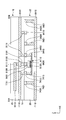
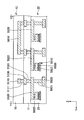
- FIG. 1 is a cross-sectional view showing an outline of the semiconductor device according to the first embodiment.
- FIG. 2 is a diagram showing the layout of the first chip in the first embodiment.
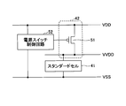
- FIG. 3 is a circuit diagram showing a configuration of a circuit included in the semiconductor device according to the first embodiment.
- FIG. 4 is a circuit diagram showing a buffer configuration.
- FIG. 5 is a schematic view showing a planar configuration of the buffer.
- FIG. 6 is a circuit diagram showing the configuration of the inverter.
- FIG. 7 is a schematic view showing a planar configuration of the inverter.
- FIG. 8 is a schematic diagram showing an outline of the power domain in the first embodiment.
- FIG. 9 is a schematic view (No. 1) showing a planar configuration of the semiconductor device according to the first embodiment.
- FIG. 1 is a cross-sectional view showing an outline of the semiconductor device according to the first embodiment.
- FIG. 2 is a diagram showing the layout of the first chip in the first embodiment.
- FIG. 10 is a schematic view (No. 2) showing a planar configuration of the semiconductor device according to the first embodiment.
- FIG. 11 is a cross-sectional view (No. 1) showing the semiconductor device according to the first embodiment.
- FIG. 12 is a cross-sectional view (No. 2) showing the semiconductor device according to the first embodiment.
- FIG. 13 is a schematic view showing a planar configuration of the semiconductor device according to the second embodiment.
- FIG. 14 is a schematic view showing a planar configuration of the semiconductor device according to the third embodiment.
- FIG. 15 is a cross-sectional view showing the semiconductor device according to the third embodiment.
- FIG. 16 is a schematic view showing a planar configuration of the semiconductor device according to the fourth embodiment.
- FIG. 17 is a cross-sectional view showing the semiconductor device according to the fourth embodiment.
- FIG. 18 is a schematic view showing a planar configuration of the semiconductor device according to the fifth embodiment.
- FIG. 19 is a schematic view showing a planar configuration of the semiconductor device according to the sixth embodiment.
- FIG. 20 is a schematic diagram showing an outline of the power domain in the seventh embodiment.
- FIG. 21 is a schematic view showing a planar configuration of the semiconductor device according to the seventh embodiment.
- FIG. 22 is a schematic view showing a planar configuration of the semiconductor device according to the eighth embodiment.
- FIG. 23 is a cross-sectional view showing the semiconductor device according to the eighth embodiment.
- FIG. 24 is a schematic view showing an outline of the planar configuration of the semiconductor device according to the ninth embodiment.
- FIG. 25 is a cross-sectional view showing an outline of the semiconductor device according to the ninth embodiment.
- FIG. 26 is a schematic view showing a planar configuration of the semiconductor device according to the ninth embodiment.
- FIG. 27 is a cross-sectional view showing the configuration of the semiconductor device according to the ninth embodiment.
- FIG. 28 is a schematic view showing a planar configuration of the semiconductor device according to the tenth embodiment.
- FIG. 29 is a cross-sectional view showing the semiconductor device according to the eleventh embodiment.
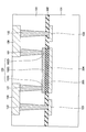
- FIG. 30 is a cross-sectional view (No. 1) showing an example of the cross-sectional configuration of the switch transistor.
- FIG. 31 is a cross-sectional view (No. 2) showing an example of the cross-sectional configuration of the switch transistor.
- FIG. 1 is a cross-sectional view showing an outline of the semiconductor device according to the first embodiment.
- the semiconductor device according to the first embodiment includes a first chip 10 and a second chip 20.
- the first chip 10 is, for example, a semiconductor chip, and includes a substrate 11 and a first wiring layer 12.
- the substrate 11 is, for example, a silicon substrate, and a semiconductor element such as a transistor is formed on the surface side of the substrate 11.
- the transistor is, for example, a FinFET with fins 13 in the source, drain and channels.
- the first wiring layer 12 is formed on the surface of the substrate 11 and includes the wiring 14 and the insulating layer 15. A part of the wiring 14 is connected to the fin 13.
- a power supply line 16 connected to the wiring 14 is formed on the front surface side of the substrate 11, and the substrate 11 is provided with a via 17 extending from the power supply line 16 to the back surface of the substrate 11.
- the via 17 is, for example, a through-silicon via (TSV).
- TSV through-silicon via
- the second chip 20 is, for example, a semiconductor chip, and is arranged so as to face the back surface of the substrate 11 of the first chip 10.
- the second chip 20 includes, for example, a second wiring layer 22 and a pad 23.
- the second wiring layer 22 includes the wiring 24 and the insulating layer 25.
- the upper surface of the second wiring layer 22 faces, for example, the back surface of the substrate 11 of the first chip 10. That is, the substrate 11 is located between the first wiring layer 12 and the second wiring layer 22.
- the second wiring layer 22 may have a plurality of wirings 24.
- the plurality of wirings 24 may be connected via vias 28 provided in the second wiring layer 22.
- the pad 23 is an external connection terminal connected to, for example, a wiring board or a board. A part of the wiring 24 is connected to the via 17.
- the pad 23 is provided on the back surface of the second wiring layer 22, and is connected to the wiring 24 through the via 28.
- the power supply potential is supplied and the signal is transmitted to the second wiring layer 22 via the
- the second chip 20 may have a size similar to that of the first chip 10, or may have a size larger than that of the first chip 10. Further, the pad 23 may be provided on the surface of the second chip 20 on the side facing the first chip 10 and outside the first chip 10 in a plan view.
- the plan view means the plan view of the surface of the first chip 10.
- the second wiring layer 22 may be provided by forming the wiring 24, the insulating layer 25, and the like on the back surface of the substrate 11.
- the second wiring layer 22 may be formed on the second substrate on which the TSV is formed, or the pad 23 may be provided on the back surface of the second substrate.
- FIG. 1 shows an outline of the semiconductor device, and the details are shown in FIGS. 9 to 12.
- FIG. 2 is a diagram showing the layout of the first chip 10.
- the first chip 10 includes a first power domain 31A, a second power domain 31B, and an input / output (I / O) cell area 32.
- the I / O cell region 32 is arranged, for example, around the first power domain 31A and the second power domain 31B.
- the number of the first power domain 31A and the number of the second power domain 31B may be 2 or more.
- FIG. 3 is a circuit diagram showing a configuration of a circuit included in the semiconductor device according to the first embodiment.
- the semiconductor device includes a standard cell 41, a power switch circuit 42, and a power switch control circuit 52.
- the power switch control circuit 52 is provided in the first power domain 31A of the first chip 10.
- the standard cell 41 is provided in the second power domain 31B of the first chip 10.
- the standard cell 41 includes various logic circuits such as a NAND circuit and an inverter.
- the power switch control circuit 52 includes a buffer as described later.
- a VSS wiring that supplies the ground potential to the power switch control circuit 52 and a VDD wiring that supplies the power potential are arranged in the second power domain 31B.
- a VSS wiring for supplying the ground potential and a V VDD wiring for supplying the power supply potential are arranged in the standard cell 41.
- the power switch circuit 42 is provided on the second chip 20.
- the power switch circuit 42 includes a switch transistor 51.
- the switch transistor 51 is, for example, a P-channel MOS transistor, and is connected between the VDD wiring and the V VDD wiring.
- the power switch control circuit 52 is connected to the gate of the switch transistor 51 and controls the operation of the switch transistor 51.
- the power switch control circuit 52 switches the switch transistor 51 on / off, and controls the continuity between the VDD wiring and the V VDD wiring.
- the power switch control circuit 52 includes, for example, a buffer.
- the switch transistor 51 may be composed of a thin film transistor (TFT), or may be a microelectromechanical systems (MEMS) switch.
- TFT thin film transistor
- MEMS microelectromechanical systems
- VSS wiring that supplies the ground potential to the first power domain 31A and a VVSS wiring that supplies the ground potential to the second power domain 31B, and N as a switch transistor 51 between the VSS wiring and the VVSS wiring.
- a channel MOS transistor may be provided.
- FIG. 4 is a circuit diagram showing a buffer configuration.
- FIG. 5 is a schematic view showing a planar configuration of the buffer.
- the buffer 60 included in the power switch control circuit 52 includes an inverter 61 and an inverter 62.
- the input signal IN is input to the inverter 61
- the output of the inverter 61 is input to the gate of the switch transistor 51 and the inverter 62
- the output signal OUT is output from the inverter 62.
- the inverter 61 includes a P-channel MOS transistor 610P and an N-channel MOS transistor 610N.
- the inverter 62 includes a P-channel MOS transistor 620P and an N-channel MOS transistor 620N.
- a power supply line 1110 corresponding to VDD wiring and a power supply line 1120 corresponding to VSS wiring are provided.
- the power lines 1110 and 1120 extend in the X direction.
- a semiconductor fin 651 extending in the X direction is provided on the power supply line 1120 side of the power supply line 1110.
- a semiconductor fin 652 extending in the X direction is provided on the power supply line 1120 side of the fin 651.
- a local wiring 631 is provided which is connected to the power supply line 1110 via the via 681, extends in the Y direction, and is connected to the fin 651.
- a local wiring 632 that is connected to the power supply line 1120 via the via 682, extends in the Y direction, and is connected to the fin 652 is provided.
- Local wiring 634 connected to fins 651 and 652 is provided on the positive side in the X direction from the local wirings 631 and 632.
- Local wiring 636 connected to fins 651 and 652 is provided on the negative side in the X direction from the local wirings 631 and 632.
- a gate electrode 612 that intersects the fins 651 and 652 via a gate insulating film (not shown) is provided between the local wiring 631 and the local wiring 634, and between the local wiring 632 and the local wiring 634.
- a gate electrode 622 that intersects the fins 651 and 652 via a gate insulating film (not shown) is provided between the local wiring 631 and the local wiring 636, and between the local wiring 632 and the local wiring 636.
- the gate electrode 612 is connected to wiring 611 via local wiring 633 and via 641.
- the gate electrode 622 is connected to the control signal line 5110 via the local wiring 635 and via 643.
- the control signal line 5110 is also connected to the local wiring 634 via the via 642.
- the local wiring 636 is connected to the wiring 621 via the via 644.
- the input signal IN is input to the wiring 611, and the output signal OUT is output from the wiring 621 (see FIG. 4).
- the control signal line 5110 is connected to the gate of the switch transistor 51. That is, the control signal line 5110 functions as a signal line for transmitting a control signal to the switch transistor 51.
- the configurations of the inverters 61 and 62 are examples.
- the number of pairs of P-channel MOS transistors and N-channel MOS transistors included in the inverters 61 and 62 may be two or more.
- the wiring connected to the gate of the switch transistor 51 may be connected to the input or output of the buffer 60.
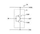
- FIG. 6 is a circuit diagram showing the configuration of the inverter.
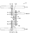
- FIG. 7 is a schematic view showing a planar configuration of the inverter.
- the inverter 70 includes a P-channel MOS transistor 710P and an N-channel MOS transistor 710N.
- a power supply line 2110 corresponding to VSS wiring and a power supply line 2120 corresponding to VSS wiring are provided.
- the power lines 2110 and 2120 extend in the X direction.
- Semiconductor fins 751 extending in the X direction are provided on the power supply line 2120 side of the power supply line 2110.
- two fins 751 are provided.
- a semiconductor fin 752 extending in the X direction is provided on the power supply line 2120 side of the fin 751.
- a local wiring 731 that is connected to the power supply line 2110 via the via 781, extends in the Y direction, and is connected to the fin 751 is provided.
- a local wiring 732 connected to the power supply line 2120 via the via 782, extending in the Y direction, and connected to the fin 752 is provided.
- Local wiring 734 connected to fins 751 and 752 is provided on the positive side in the X direction from the local wirings 731 and 732.
- a gate electrode 712 that intersects the fins 751 and 752 via a gate insulating film (not shown) is provided between the local wiring 731 and the local wiring 734, and between the local wiring 732 and the local wiring 734.
- the gate electrode 712 is connected to the wiring 711 via the local wiring 733 and the via 741.
- the local wiring 734 is connected to the wiring 760 via the via 742.
- the input signal IN is input to the wiring 711, and the output signal OUT is output from the wiring 760 (see FIG. 6).
- the circuit included in the standard cell 41 is not limited to the inverter, and circuits such as various logic circuits may be included. Further, a memory cell of SRAM (Static Random Access Memory) may be included. Further, the circuit may be provided over the region where the power supply lines 2110 and 2120 are three or more. That is, a so-called multi-height circuit may be provided.
- SRAM Static Random Access Memory
- FIGS. 5 and 7 exemplify a transistor using fins (FinFET), a planar type transistor and a complementary field effect transistor (Complementary) are used in the first power domain 31A and the second power domain 31B.
- FieldEffectTransistor (CFET), a transistor using nanowires, and the like may be provided.
- FIG. 8 is a schematic diagram showing an outline of the power domain in the first embodiment.
- the second power domain 31B is located on the positive side of the first power domain 31A in the X direction.
- the first power domain 31A includes circuits connected to power lines 1110 and 1120.
- the buffer 60 of the power switch control circuit 52 shown in FIGS. 4 and 5 is included in the first power domain 31A.
- the second power domain 31B includes circuits connected to power lines 2110 and 2120.
- the inverter 70 shown in FIGS. 6 and 7 is included in the second power domain 31B.
- the power switch circuit 42 is located between the first power domain 31A and the second power domain 31B.
- the power line 1110 and the power line 2110 extend along the extending direction as shown in FIG. At least a part of the power domain 31A of 1 and the second power domain 31B may be arranged.
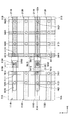
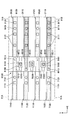
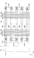
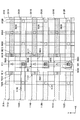
- FIGS. 9 and 10 are schematic views showing a planar configuration of the semiconductor device according to the first embodiment.
- 11 and 12 are cross-sectional views showing a semiconductor device according to the first embodiment.
- FIG. 9 shows the internal configuration of the first chip 10 and the second chip 20, and
- FIG. 10 shows the internal configuration of the second chip 20.
- FIG. 11 corresponds to a cross-sectional view taken along the line X11-X21 in FIGS. 9 and 10
- FIG. 12 corresponds to a cross-sectional view taken along the line X12-X22 in FIGS. 9 and 10.
- the power supply lines 1110 extending in the X direction and the power supply lines 1120 extending in the X direction are alternately arranged in the Y direction.
- the power supply line 1110 corresponds to the VDD wiring
- the power supply line 1120 corresponds to the VSS wiring.
- a plurality of grooves extending in the X direction are formed on the substrate 11, and the power supply lines 1110 and 1120 are formed in these grooves.
- the power supply lines 1110 and 1120 having such a structure are sometimes called BPR (Buried Power Rail).
- An element separation film (not shown) may be formed on the surface of the substrate 11.
- the element separation membrane is formed by, for example, the STI (Shallow Trench Isolation) method. The surface of the element separation membrane may or may not be flush with the surface of the substrate 11.
- Vias 1111 and 1121 that penetrate the substrate 11 to the back surface are formed on the substrate 11.
- the via 1111 is formed below the power line 1110 and the via 1121 is formed below the power line 1120.
- One power supply line 1110 may be provided with two or more vias 1111 or one power supply line 1120 may be provided with two or more vias 1121.
- a circuit such as the power switch control circuit 52 shown in FIG. 5 is connected between the power supply line 1110 and the power supply line 1120.
- the control signal line 5110 that transmits the output of the inverter 61 is located between the power supply line 1110 and the power supply line 1120 in a plan view.
- the control signal line 5110 extends to the region between the first power domain 31A and the second power domain 31B in plan view.
- a groove is formed in the substrate 11 below the end of the control signal line 5110 on the second power domain 31B side, and the connection layer 5190 is formed in the groove.
- the insulating layer 15 is formed with vias 5111 that electrically connect the control signal line 5110 and the connecting layer 5190.
- a via 5191 that penetrates the substrate 11 to the back surface is formed on the substrate 11.
- the via 5191 is formed below the connecting layer 5190.
- the power supply lines 2110 extending in the X direction and the power supply lines 2120 extending in the X direction are alternately arranged in the Y direction.
- the power supply line 2110 corresponds to the VSS wiring
- the power supply line 2120 corresponds to the VSS wiring.
- a plurality of grooves extending in the X direction are formed on the substrate 11, and the power supply lines 2110 and 2120 are formed in these grooves.
- Power lines 2110 and 2120 having such a structure may also be referred to as BPR.
- An element separation film (not shown) may be formed on the surface of the substrate 11.
- Vias 2111 and 2121 are formed on the substrate 11 so as to penetrate the substrate 11 to the back surface.
- the via 2111 is formed below the power supply line 2110 and the via 2121 is formed below the power supply line 2120.
- One power supply line 2110 may be provided with two or more vias 2111, or one power supply line 2120 may be provided with two or more vias 2121.
- the circuit included in the standard cell 41 such as the inverter 70 shown in FIG. 7 is connected between the power supply line 2110 and the power supply line 2120.
- a memory cell of the SRAM may be connected between the power supply line 2110 and the power supply line 2120.
- the second chip 20 includes, for example, an insulating layer 25 and power supply lines 7110, 7120, 8110, and 8120 formed on the surface layer portion of the insulating layer 25.
- the power lines 7110, 7120, 8110 and 8120 extend in the X direction.
- the power supply lines 7110 and 7120 are provided in an area overlapping the first power domain 31A in a plan view.
- the power supply line 7110 corresponds to the VDD wiring
- the power supply line 7120 corresponds to the VSS wiring.
- the power supply line 7110 overlaps with the power supply line 1110 and is connected to the power supply line 1110 via the via 1111.
- the power supply line 7120 overlaps the power supply line 1120 and is connected to the power supply line 1120 via the via 1121.
- a power supply line 7112 is provided below the power supply line 7110, and a via 7111 for connecting the power supply line 7112 and the power supply line 7110 is provided.
- a power supply line 7122 may be provided below the power supply line 7120, or a via 7121 connecting the power supply line 7122 and the power supply line 7120 may be provided.
- the power supply lines 7112 and 7122 may extend in the X direction or may extend in the Y direction.
- the power line 7122 and via 7121 may not be provided.
- the power supply lines 8110 and 8120 are provided in an area overlapping the second power domain 31B in a plan view.
- the power supply line 8110 corresponds to the VSS wiring
- the power supply line 8120 corresponds to the VSS wiring.
- the power supply line 8110 overlaps with the power supply line 2110 and is connected to the power supply line 2110 via the via 2111.
- the power supply line 8120 overlaps with the power supply line 2120 and is connected to the power supply line 2120 via via 2121.
- a power supply line 8112 may be provided below the power supply line 8110, or a via 8111 connecting the power supply line 8112 and the power supply line 8110 may be provided.
- FIG. 11 a power supply line 8112 may be provided below the power supply line 8110, or a via 8111 connecting the power supply line 8112 and the power supply line 8110 may be provided.
- a power supply line 8122 may be provided below the power supply line 8120, or a via 8121 connecting the power supply line 8122 and the power supply line 8120 may be provided.
- the power lines 8112 and 8122 may extend in the X direction or may extend in the Y direction.
- the second chip 20 includes a gate electrode 5120 in the insulating layer 25.
- the gate electrode 5120 is located below the power lines 7110, 7120, 8110 and 8120.
- the gate electrode 5120 is located between the first power domain 31A and the second power domain 31B.
- a connecting portion 5180 is formed on the surface layer portion of the insulating layer 25 above the gate electrode 5120.
- the connecting portion 5180 is connected to the via 5191.
- the insulating layer 25 is formed with vias 5181 that electrically connect the gate electrode 5120 and the connecting portion 5180.
- a plurality of semiconductor layers 6110 overlapping the power supply lines 7110 and 8110 are formed in the insulating layer 25 in a plan view.
- the semiconductor layer 6110 is located below the gate electrode 5120, and a gate insulating film 6120 is provided between the semiconductor layer 6110 and the gate electrode 5120.
- the gate insulating film 6120 is in contact with the gate electrode 5120, and the semiconductor layer 6110 is in contact with the gate insulating film 6120.
- the semiconductor layer 6110 has a V VDD connection portion 6111 (drain) and a VDD connection portion 6112 (source) with the center line of the semiconductor layer 6110 sandwiched in the X direction.
- the insulating layer 25 is formed with a via 8113 that electrically connects the V VDD connection portion 6111 and the power supply line 8110, and a via 7113 that electrically connects the VDD connection portion 6112 and the power supply line 7110.
- the plurality of semiconductor layers 6110 are arranged in the Y direction.
- the power supply line 7110 is connected to the VDD connection portion 6112 via the via 7113. Further, the V VDD connection unit 6111 is connected to the power supply line 2110 via the via 8113, the power supply line 8110, and the via 2111. The potential of VDD is supplied to the power supply line 7110 via, for example, the power supply line 7112 which is a part of the pad 23 (see FIG. 1). Further, as described above, the power supply line 2110 corresponds to the V VDD wiring.
- the conduction between the V VDD connection portion 6111 and the VDD connection portion 6112 is controlled by the potential of the gate electrode 5120. That is, the gate electrode 5120 functions as a gate of the switch transistor 51 connected between the VDD wiring and the V VDD wiring.
- the switch transistor 51 includes the semiconductor layer 6110, and the semiconductor layer 6110 is located between the first power domain 31A and the second power domain 31B in a plan view. That is, in a plan view, the switch transistor 51 is located between the first power domain 31A and the second power domain 31B.
- an area for power supply separation is provided between the first power domain 31A and the second power domain 31B. Therefore, according to the present embodiment, in the first chip 10, between the first power domain 31A and the second power domain 31B, in addition to the region for power supply separation (separation region), the switch transistor The size of the semiconductor device can be reduced as compared with the case where the 51 is arranged.
- connection layer 5190 having the same structure as the BPR can be used for connecting the control signal line 5110 and the connection portion 5180.
- the number of vias 2111 and 2121 is not limited. As the number of vias 2111 and 2121 increases, the resistance between the power supply line 2110 and the power supply line 8110 and the resistance between the power supply line 2120 and the power supply line 8120 can be lowered, and IR drop can be suppressed.
- the power supply lines 7112, 7122, 8112 and 8122 may extend in the Y direction.
- the power line 8112 may not be provided.
- each via is not particularly limited, and may be, for example, a circle, an ellipse, a square, a rectangle, or the like.
- FIG. 13 is a schematic view showing a planar configuration of the semiconductor device according to the second embodiment.
- a semiconductor layer 6210 is provided instead of the plurality of semiconductor layers 6110.
- the semiconductor layer 6210 overlaps with the power supply lines 7110 and 8110 in a plan view and extends in the Y direction.
- a gate electrode 5220 extending in the Y direction is provided above the semiconductor layer 6210.
- a gate insulating film (not shown) is provided between the gate electrode 5220 and the semiconductor layer 6210 in place of the gate insulating film 6120. The gate insulating film is in contact with the gate electrode 5220, and the semiconductor layer 6210 is in contact with the gate insulating film.
- the semiconductor layer 6210 has a V VDD connection portion 6211 and a VDD connection portion 6212 with the center line of the semiconductor layer 6210 interposed therebetween in the X direction.
- the insulating layer 25 is formed with a via 8113 that electrically connects the V VDD connection portion 6211 and the power supply line 8110, and a via 7113 that electrically connects the VDD connection portion 6212 and the power supply line 7110.
- a plurality of power supply lines 8110 are connected to one V VDD connection unit 6211 via a plurality of vias 8113
- a plurality of power supply lines 7110 are connected to one VDD connection unit 6212 via a plurality of vias 7113.
- the switch transistor 51 includes a semiconductor layer 6210, and the semiconductor layer 6210 is located between the first power domain 31A and the second power domain 31B in a plan view. That is, in a plan view, the switch transistor 51 is located between the first power domain 31A and the second power domain 31B.
- the size of the semiconductor device can be reduced as in the first embodiment. In addition, efficiency can be improved.
- FIG. 14 is a schematic view showing a planar configuration of the semiconductor device according to the third embodiment.
- FIG. 15 is a cross-sectional view showing the semiconductor device according to the third embodiment.
- FIG. 15 corresponds to a cross-sectional view taken along the line X13-X23 in FIG.
- a power supply line 7320 is provided in place of the power supply lines 7120 and 8120.
- the power supply line 7320 is provided on the surface layer portion of the insulating layer 25.
- the power line 7320 extends in the X direction.
- the power supply line 7320 is provided in a region overlapping the first power domain 31A, a region overlapping the second power domain 31B, and a region between them in a plan view.
- the power line 7320 corresponds to VSS wiring.
- the power supply line 7320 overlaps the power supply lines 1120 and 2120 in a plan view, and is connected to the power supply lines 1120 and 2120 via vias 1121 and 2121.
- a power supply line 7322 may be provided below the power supply line 7320 instead of the power supply lines 7122 and 8122, and the power supply line 7322 is connected to the power supply line 7320 via vias 7121 and 8121. You may be.
- the same effect as that of the first embodiment can be obtained by the third embodiment. Further, in the third embodiment, since the VSS wiring is shared between the first power domain 31A and the second power domain 31B, the power supply noise generated in the VDD wiring can be reduced.
- FIG. 16 is a schematic view showing a planar configuration of the semiconductor device according to the fourth embodiment.
- FIG. 17 is a cross-sectional view showing the semiconductor device according to the fourth embodiment.
- FIG. 17 corresponds to a cross-sectional view taken along the line X14-X24 in FIG.
- power supply lines 7410, 7420, 8410 and 8420 are provided in place of the power supply lines 7110, 7120, 8110 and 8120.
- the power supply lines 7410, 7420, 8410 and 8420 are provided on the surface layer portion of the insulating layer 25.
- the power lines 7410, 7420, 8410 and 8420 extend in the Y direction.
- the power supply lines 7410 and 7420 are provided in a region overlapping the first power domain 31A in a plan view.
- the power supply line 7410 corresponds to the VDD wiring
- the power supply line 7420 corresponds to the VSS wiring.
- the power supply line 7410 is orthogonal to the power supply lines 1110 and 1120 and is connected to the power supply line 1110 via vias 1111.
- the power supply line 7420 is orthogonal to the power supply lines 1110 and 1120 and is connected to the power supply line 1120 via the via 1121.
- a power supply line 7112 may be provided below the power supply line 1110, and a via 7421 connecting the power supply line 7112 and the power supply line 7420 may be provided.
- a power supply line (not shown) corresponding to VDD wiring is provided below the power supply line 1120, and as shown in FIG. 16, a via 7411 for connecting the power supply line and the power supply line 7410 is provided.
- the power lines 1110 and 7410 have a mesh structure in a plan view.
- the power lines 1120 and 7420 have a mesh structure in a plan view.
- the power supply lines 8410 and 8420 are provided in an area overlapping the second power domain 31B in a plan view.
- the power supply line 8410 corresponds to the VSS wiring
- the power supply line 8420 corresponds to the VSS wiring.
- the power supply line 8410 is orthogonal to the power supply lines 2110 and 2120 and is connected to the power supply line 2110 via vias 2111.
- the power supply line 8420 is orthogonal to the power supply lines 2110 and 2120 and is connected to the power supply line 2120 via via 2121.
- a power supply line 8112 may be provided below the power supply line 2110, and a via 8421 connecting the power supply line 8112 and the power supply line 8420 may be provided.
- a power supply line (not shown) corresponding to the V VDD wiring is provided below the power supply line 2120, and as shown in FIG. 16, a via 8411 for connecting the power supply line and the power supply line 8410 is provided.
- the power lines 2110 and 8410 have a mesh structure in a plan view.
- the power lines 2120 and 8420 have a mesh structure in a plan view.
- a plurality of power supply lines 1110 can be commonly connected to the VDD connection portion 6412 of each switch transistor 51, and a plurality of power supply lines 2110 can be commonly connected to the V VDD connection portion 6411 of each switch transistor 51. Further, the power supply can be redistributed via the power supply lines 7112, 8112 and the like.
- the number of power lines 7410, 7420, 8410 and 8420 is not limited.
- the width of the power supply line 7410 connected to the VDD connection portion 6412 via the via 7413 among the plurality of power supply lines 7410 may be larger than the width of the other power supply lines 7410. .
- the width of the power supply line 8410 connected to the V VDD connection portion 6411 via the via 8413 among the plurality of power supply lines 8410 may be larger than the width of the other power supply lines 8410. ..
- FIG. 18 is a schematic view showing a planar configuration of the semiconductor device according to the fifth embodiment. In FIG. 18, the portion corresponding to the control signal line 5110 is omitted.
- a semiconductor layer 6510 is provided in place of the plurality of semiconductor layers 6110, a power supply line 7510 is provided in place of the power supply line 7110, and a power supply line is provided in place of the power supply line 8110. 8510 is provided.
- the power supply line 7510 corresponds to the VDD wiring, and the power supply line 8510 corresponds to the V VDD wiring.
- the power supply line 7510 is provided in a region overlapping the first power domain 31A in a plan view.
- the power supply line 7510 further extends between the first power domain 31A and the second power domain 31B to the vicinity of the power supply line 8120.
- the power supply line 8510 is provided in a region overlapping the second power domain 31B in a plan view.
- the power supply line 8510 further extends between the first power domain 31A and the second power domain 31B to the vicinity of the power supply line 7120. Then, in the Y direction view, the power supply lines 7510 and 8510 overlap each other.
- the semiconductor layer 6510 overlaps with the power supply lines 7510 and 8510 in a plan view and extends in the Y direction. Further, instead of the gate electrode 5120, a gate electrode 5520 extending in the X direction is provided above the semiconductor layer 6510. The gate electrode 5520 is located between the end of the power supply line 7510 on the power supply line 8120 side and the end of the power supply line 8510 on the power supply line 7120 side, which are adjacent to each other in the Y direction.
- the semiconductor layer 6110 has a VDD connection portion 6512 around the end portion of the power supply line 7510 on the power supply line 8120 side in a plan view, and a V VDD connection portion around the end portion of the power supply line 8510 on the power supply line 7120 side in a plan view.
- a gate insulating film (not shown) is provided between the gate electrode 5520 and the semiconductor layer 6510 in place of the gate insulating film 6120.
- the gate insulating film is in contact with the gate electrode 5520, and the semiconductor layer 6510 is in contact with the gate insulating film.
- the insulating layer 25 is formed with vias 8513 that electrically connect the V VDD connection portion 6511 and the power supply line 8510, and vias 7513 that electrically connect the VDD connection portion 6512 and the power supply line 7510.
- FIG. 19 is a schematic view showing a planar configuration of the semiconductor device according to the sixth embodiment. In FIG. 19, the portion corresponding to the control signal line 5110 is omitted.
- a common connection portion 7610 is provided which is commonly connected to two power supply lines 7110 adjacent to each other with one power supply line 7120 sandwiched in the Y direction. ..
- the common connection portion 7610 is connected to the end of the power supply line 7110 on the second power domain 31B side, and extends to a region between the first power domain 31A and the second power domain 31B in a plan view.
- the end of the common connection portion 7610 on the second power domain 31B side is located in the vicinity of the second power domain 31B.
- the power supply line 7120 between the two power supply lines 7110 connected to the common connection portion 7610 is separated from the common connection portion 7610 in the X direction.
- a common connection portion 8610 is provided which is commonly connected to two adjacent power supply lines 8110 with one power supply line 8120 sandwiched in the Y direction.
- the common connection portion 8610 is connected to the end of the power supply line 8110 on the first power domain 31A side, and extends to a region between the first power domain 31A and the second power domain 31B in a plan view.
- the end of the common connection portion 8610 on the first power domain 31A side is located in the vicinity of the first power domain 31A.
- the power supply line 8120 between the two power supply lines 8110 connected to the common connection portion 8610 is separated from the common connection portion 8610 in the X direction.
- a semiconductor layer 6610 is provided in place of the semiconductor layer 6110. Each semiconductor layer 6610 is arranged so as to overlap a part of the common connection portion 8610 adjacent to each other in the Y direction and a part of the common connection portion 7610. Further, instead of the gate electrode 5120, a gate electrode 5620 extending in the X direction is provided above the semiconductor layer 6610. The gate electrode 5620 is located between the common connection portion 8610 and the common connection portion 7610, which are adjacent to each other in the Y direction.
- the semiconductor layer 6610 has a VDD connection portion 6612 around the common connection portion 7610 in a plan view, and has a V VDD connection portion 6611 around the common connection portion 8610 in a plan view.
- a gate insulating film (not shown) is provided between the gate electrode 5620 and the semiconductor layer 6610 in place of the gate insulating film 6120.
- the gate insulating film is in contact with the gate electrode 5620, and the semiconductor layer 6610 is in contact with the gate insulating film.
- the insulating layer 25 is formed with a via 8613 that electrically connects the V VDD connection portion 6611 and the common connection portion 8610, and a via 7613 that electrically connects the VDD connection portion 6612 and the common connection portion 7610. .
- each common connection portion 7610 is connected to the VDD connection portion 6612 of the two switch transistors 51, and each common connection portion 8610 is connected to the V VDD connection portion 6611 of the two switch transistors 51.
- FIG. 20 is a schematic diagram showing an outline of the power domain in the seventh embodiment.
- FIG. 21 is a schematic view showing a planar configuration of the semiconductor device according to the seventh embodiment.
- the third power domain 31C is provided on the negative side in the Y direction of the second power domain 31B.
- the third power domain 31C like the first power domain 31A, includes circuits connected to power lines 1110 and 1120.
- the power switch circuit 42 is provided between the third power domain 31C and the second power domain 31B.
- the second power domain 31B is arranged surrounded by the third power domain 31C, as shown in FIG. 20, in the direction orthogonal to the extending direction of the power supply line 1110 and the power supply line 2110. Along the line, at least a part of the third power domain 31C and the second power domain 31B may be arranged.
- power lines 2110, 2120, 8410, 8420 and the like are provided in the second power domain 31B. Further, the power supply lines 1110, 1120, 7410, 7420 and the like are provided in the third power domain 31C. Further, instead of the control signal line 5110, a control signal line 5710 extending in the Y direction is provided. The control signal line 5710 is connected to the connection layer 5190 via the via 5111 (see FIG. 11). The power supply lines 7410, 7420, 8410 and 8420 are provided on the surface layer portion of the insulating layer 25 and extend in the Y direction, as in the fourth embodiment.
- a semiconductor layer 6710 is provided between the second power domain 31B and the third power domain 31C.
- the semiconductor layer 6710 overlaps with the power supply lines 7410 and 8410 in a plan view and extends in the X direction.
- a gate electrode 5720 extending in the X direction is provided above the semiconductor layer 6710.
- a gate insulating film (not shown) is provided between the gate electrode 5720 and the semiconductor layer 6710. The gate insulating film is in contact with the gate electrode 5720, and the semiconductor layer 6710 is in contact with the gate insulating film.
- the semiconductor layer 6710 has a V VDD connection portion 6711 and a VDD connection portion 6712 with the center line of the semiconductor layer 6710 interposed therebetween in the Y direction.
- the insulating layer 25 is formed with vias 8713 that electrically connect the V VDD connection portion 6711 and the power supply line 8410, and vias 7713 that electrically connect the VDD connection portion 6712 and the power supply line 7410.
- a plurality of power supply lines 8410 are connected to one V VDD connection unit 6711 via a plurality of vias 8713
- a plurality of power supply lines 7410 are connected to one VDD connection unit 6712 via a plurality of vias 7713.
- the configuration of the switch transistor 51 provided in the seventh embodiment follows the configuration of the switch transistor 51 in the second embodiment.
- the configuration of the switch transistor 51 provided between the second power domain 31B and the third power domain 31C may be similar to the configuration of the switch transistor 51 in another embodiment.
- each power supply line does not have to be provided on the surface layer portion of the insulating layer 25, and may be provided inside the insulating layer 25. Further, the power supply line provided on the surface layer portion of the insulating layer 25 may extend in the X direction.
- a first power domain 31A may be provided in addition to the second power domain 31B and the third power domain 31C, between the first power domain 31A and the second power domain 31B, and the second.
- a power switch circuit 42 may be provided between the power domain 31B and the third power domain 31C.
- FIG. 22 is a schematic view showing a planar configuration of the semiconductor device according to the eighth embodiment.
- FIG. 23 is a cross-sectional view showing the semiconductor device according to the eighth embodiment.
- FIG. 23 corresponds to a cross-sectional view taken along the line X15-X25 in FIG.
- the semiconductor layer 6810 is provided in place of the semiconductor layer 6110.
- the semiconductor layer 6810 overlaps the power supply lines 7110 and 8110 in a plan view.
- a gate electrode 5820 is provided below the semiconductor layer 6210.
- a gate insulating film 6820 is provided between the gate electrode 5820 and the semiconductor layer 6810 instead of the gate insulating film 6120. The gate insulating film 6820 is in contact with the gate electrode 5820, and the semiconductor layer 6810 is in contact with the gate insulating film 6820.
- the gate electrode 5820 may be formed in the same layer as the power supply lines 7112 and 8112.
- the gate electrode 5820 may be formed of the same material as the power supply lines 7112 and 8112 and the like.
- the control signal line 5110 may extend in the Y direction and be connected to a plurality of gate electrodes 5820 via a plurality of vias 5111 and the like.
- the gate electrode and the gate insulating film may be located below the semiconductor layer.
- FIG. 24 is a schematic view showing an outline of the planar configuration of the semiconductor device according to the ninth embodiment.
- FIG. 25 is a cross-sectional view showing an outline of the semiconductor device according to the ninth embodiment.
- a part relating to the arrangement of control signal lines, which is a characteristic part of the ninth embodiment, is illustrated, and the semiconductor layer, some power lines, vias, and the like are not shown.
- a plurality of control signal lines 5930 are arranged in the insulating layer 25.
- the control signal lines 5930 extend in the X direction and are arranged side by side in the Y direction.
- Each control signal line 5930 has a portion protruding from both ends of the second power domain 31B in the X direction.
- the control signal lines 5930 adjacent to each other in the Y direction are connected to each other via the control signal lines 5910 extending in the Y direction outside the second power domain 31B.
- the control signal line 5930 connected to the control signal line 5930 located on the positive side in the Y direction via the control signal line 5910 on the negative side in the X direction is on the negative side in the Y direction via the control signal line 5910 on the positive side in the X direction. It is connected to the located control signal line 5930.
- the control signal line 5930 connected to the control signal line 5930 located on the positive side in the Y direction via the control signal line 5910 on the positive side in the X direction is connected to the control signal line 5930 on the negative side in the X direction via the control signal line 5910 in the Y direction. It is connected to the control signal line 5930 located on the negative side.
- the control signal lines 5930 adjacent to each other in the Y direction are connected to each other only outside the second power domain 31B.
- a gate electrode (not shown) of the switch transistor 51 is connected to the control signal line 5910. That is, a plurality of switch transistors 51 are connected in parallel.
- FIG. 26 is a schematic view showing a planar configuration of the semiconductor device according to the ninth embodiment.
- FIG. 27 is a cross-sectional view showing the configuration of the semiconductor device according to the ninth embodiment.
- FIG. 27 corresponds to a cross-sectional view taken along the line Y11-Y21 in FIG. 26.
- control signal line 5930 extends in the X direction below the semiconductor layer 6410.
- a connecting portion 5920 is provided at a portion of the surface layer portion of the insulating layer 25 that overlaps with the control signal line 5110 or 5910 in a plan view.
- a via 5921 is provided to electrically connect the control signal line 5930 and the connecting portion 5920.
- a via 5922 is provided below the connecting portion 5920 in addition to the via 5921.
- a gate electrode 5923 connected to the via 5922 is provided, and a gate insulating film 6920 and a semiconductor layer 6910 are provided under the gate electrode 5923.
- the semiconductor layer 6910 has a V VDD connection portion 6911 and a VDD connection portion 6912 with the center line of the semiconductor layer 6910 interposed therebetween in the X direction.
- the insulating layer 25 includes a via 8913 that electrically connects the V VDD connection portion 6911 and the power supply line 8110 (see FIGS. 9 to 12), and a VDD connection portion 6912 and the power supply line 7110 (see FIGS. 9 to 12).
- a via 7913 is formed to electrically connect the two.
- the plurality of semiconductor layers 6910 are arranged in the Y direction.
- the switch transistor 51 is provided in the region where the control signal line 5930 and the control signal line 5110 or 5910 intersect in a plan view.
- the capacitance and resistance parasitic on the control signal line 5930 are large. Then, the control signal from the power switch control circuit is sequentially transmitted to each switch transistor 51 through the control signal line 5930. Therefore, the rise of the V VDD potential in the second power domain 31B becomes gentle, and the power supply noise due to the steep rise of the potential can be reduced.
- control signal lines 5930 adjacent to each other in the Y direction are connected outside the second power domain 31B in a plan view via a control signal line provided on the surface layer of the second chip 20 instead of the control signal line 5910. It may have been done.
- FIG. 28 is a schematic view showing a planar configuration of the semiconductor device according to the tenth embodiment.
- a part relating to the arrangement of control signal lines, which is a characteristic part of the tenth embodiment, is shown, and the semiconductor layer, some power lines, vias, and the like are not shown.
- a buffer 5700 is added to the control signal lines 5110 and 5910.
- the buffer 5700 is provided on the first chip 10.
- the buffer 5700 is supplied with voltage from the VDD wiring and the VSS wiring in the same manner as the buffer 60.
- the buffer 5700 may be provided in the first power domain 31A in the same manner as the buffer 60.
- Other configurations are the same as in the ninth embodiment.
- the buffer 5700 can function as a delay circuit. Therefore, the operation timing of the switch transistor 51 can be controlled by using the delay in the transmission of the control signal by the buffer 5700.
- FIG. 29 is a cross-sectional view showing the semiconductor device according to the eleventh embodiment.
- a part relating to a control signal line and a switch transistor, which are characteristic parts of the eleventh embodiment, is illustrated, and the semiconductor layer, a part of the power supply line, vias, and the like are not shown.
- the wiring capacitance unit 5941 including the wiring 5931 and the wiring 5932 adjacent to each other is connected to the control signal line 5930 via the via 5951.
- the wires 5931 and 5932 extend in the Y direction, and the via 5951 is connected to the wire 5931.
- the wiring 5933 extending in the Y direction is connected to the control signal line 5930 via the via 5952.
- An insulating film 5934 and a conductive film 5935 are formed on the wiring 5933.
- the capacitive element 5942 is composed of the wiring 5933, the insulating film 5934, and the conductive film 5935.
- the wiring capacitance unit 5941 and the capacitance element 5942 parasitize the control signal line 5930 with a larger capacitance. Therefore, the effect of suppressing the steep rise of the potential can be made higher.
- the wiring capacitance section 5941 or the capacitance element 5942 may be provided. In other embodiments, the wiring capacitance section 5941 may be provided, the capacitance element 5942 may be provided, or both of them may be provided.
- 30 and 31 are cross-sectional views showing an example of the cross-sectional configuration of the switch transistor.
- the underlying insulating film 102 is provided in the insulating layer 101, and the semiconductor layer 103, the gate insulating film 104, and the gate electrode 105 are provided on the underlying insulating film 102.
- a control signal line 110, a power supply line 120 corresponding to VDD wiring, and a power supply line 130 corresponding to V VDD wiring are provided on the surface layer portion of the insulating layer 101.
- the semiconductor layer 103 has a channel 103C and a source 103S and a drain 103D sandwiching the channel 103C.
- the power supply line 120 and the source 103S are connected via the via 121, and the power supply line 130 and the drain 103D are connected via the via 131.
- a power supply line 123 corresponding to VDD wiring and a power supply line 133 corresponding to V VDD wiring are provided under the underlying insulating film 102.
- the power supply line 120 and the power supply line 123 are connected via the via 122, and the power supply line 130 and the power supply line 133 are connected via the via 132.
- the control signal line 110 is connected to the gate electrode 105 via the via 111.
- the gate insulating film 204 is provided in the underlying insulating film 102, the semiconductor layer 103 is provided on the gate insulating film 204, and the gate electrode 205 is provided under the gate insulating film 204.
- Other configurations are the same as in the first example.
- the material of the underlying insulating film is, for example, silicon oxide, silicon nitride, silicon carbide, silicon oxide nitride, silicon oxide carbide, or the like.
- the material of the semiconductor layer is, for example, InGaZnO (IGZO), ZnO, ZnSnO, InZnO, or the like.
- the material of the gate insulating film is, for example, SiO 2 , SiO x N y , SiN, Al 2 O 3, and the like.
- the material of the gate electrode is a metal such as molybdenum, titanium, chromium, tantalum, magnesium, silver, tungsten, aluminum, copper, neodymium, ruthenium, scandium and the like.
- the material of the gate electrode may be graphene or the like.
- the switch transistors 51 provided in each of the above embodiments can be classified into the first and second examples from the viewpoint of the stacking relationship between the gate electrode and the semiconductor layer and the connection relationship between the semiconductor layer and the VDD wiring as follows. Become. That is, the switch transistors 51 provided in the first to seventh, ninth, and tenth embodiments are classified into the first example. The switch transistor 51 provided in the eighth embodiment is classified into the second example.
- the present invention has been described above based on each embodiment, the present invention is not limited to the requirements shown in the above embodiments. With respect to these points, the gist of the present invention can be changed without impairing the gist of the present invention, and can be appropriately determined according to the application form thereof.
- First chip 20 Second chip 31A, 31B, 31C: Power domain 42: Power switch circuit 51: Switch transistor 52: Power switch control circuit
Landscapes
- Semiconductor Integrated Circuits (AREA)
- Design And Manufacture Of Integrated Circuits (AREA)
- Metal-Oxide And Bipolar Metal-Oxide Semiconductor Integrated Circuits (AREA)
- Physics & Mathematics (AREA)
- Geometry (AREA)
- Thin Film Transistor (AREA)
- Internal Circuitry In Semiconductor Integrated Circuit Devices (AREA)
Priority Applications (6)
| Application Number | Priority Date | Filing Date | Title |
|---|---|---|---|
| CN201980101206.4A CN114514604B (zh) | 2019-10-11 | 2019-10-11 | 半导体装置 |
| PCT/JP2019/040258 WO2021070366A1 (ja) | 2019-10-11 | 2019-10-11 | 半導体装置 |
| JP2021551077A JP7380697B2 (ja) | 2019-10-11 | 2019-10-11 | 半導体装置 |
| US17/716,299 US12119301B2 (en) | 2019-10-11 | 2022-04-08 | Semiconductor device |
| JP2023186192A JP7529121B2 (ja) | 2019-10-11 | 2023-10-31 | 半導体装置 |
| US18/886,493 US20250006635A1 (en) | 2019-10-11 | 2024-09-16 | Semiconductor device |
Applications Claiming Priority (1)
| Application Number | Priority Date | Filing Date | Title |
|---|---|---|---|
| PCT/JP2019/040258 WO2021070366A1 (ja) | 2019-10-11 | 2019-10-11 | 半導体装置 |
Related Child Applications (1)
| Application Number | Title | Priority Date | Filing Date |
|---|---|---|---|
| US17/716,299 Continuation US12119301B2 (en) | 2019-10-11 | 2022-04-08 | Semiconductor device |
Publications (1)
| Publication Number | Publication Date |
|---|---|
| WO2021070366A1 true WO2021070366A1 (ja) | 2021-04-15 |
Family
ID=75438154
Family Applications (1)
| Application Number | Title | Priority Date | Filing Date |
|---|---|---|---|
| PCT/JP2019/040258 Ceased WO2021070366A1 (ja) | 2019-10-11 | 2019-10-11 | 半導体装置 |
Country Status (4)
| Country | Link |
|---|---|
| US (2) | US12119301B2 (https=) |
| JP (2) | JP7380697B2 (https=) |
| CN (1) | CN114514604B (https=) |
| WO (1) | WO2021070366A1 (https=) |
Cited By (6)
| Publication number | Priority date | Publication date | Assignee | Title |
|---|---|---|---|---|
| US20230057276A1 (en) * | 2021-08-18 | 2023-02-23 | Qualcomm Incorporated | Mixed pitch track pattern |
| US20240332300A1 (en) * | 2019-04-25 | 2024-10-03 | Socionext Inc. | Semiconductor device |
| WO2024252660A1 (ja) * | 2023-06-09 | 2024-12-12 | 株式会社ソシオネクスト | 半導体装置 |
| WO2025079230A1 (ja) * | 2023-10-13 | 2025-04-17 | 株式会社ソシオネクスト | 半導体装置 |
| WO2025079231A1 (ja) * | 2023-10-13 | 2025-04-17 | 株式会社ソシオネクスト | 半導体装置 |
| WO2025079229A1 (ja) * | 2023-10-13 | 2025-04-17 | 株式会社ソシオネクスト | 半導体装置 |
Families Citing this family (2)
| Publication number | Priority date | Publication date | Assignee | Title |
|---|---|---|---|---|
| US20220328409A1 (en) * | 2021-04-08 | 2022-10-13 | Taiwan Semiconductor Manufacturing Company, Ltd. | Targeted power grid structure and method |
| US20250006663A1 (en) * | 2023-06-30 | 2025-01-02 | International Business Machines Corporation | Double-sided integrated circuit with electrostatic guard ring |
Citations (7)
| Publication number | Priority date | Publication date | Assignee | Title |
|---|---|---|---|---|
| JPS5326689A (en) * | 1976-08-25 | 1978-03-11 | Hitachi Ltd | Semiconductor integrated circuit unit |
| JPH05206420A (ja) * | 1992-01-30 | 1993-08-13 | Nec Ic Microcomput Syst Ltd | 半導体集積回路 |
| JPH11102910A (ja) * | 1997-09-29 | 1999-04-13 | Hitachi Ltd | 半導体集積回路 |
| JP2009302198A (ja) * | 2008-06-11 | 2009-12-24 | Elpida Memory Inc | 半導体チップ、半導体チップ群および半導体装置 |
| JP2012044042A (ja) * | 2010-08-20 | 2012-03-01 | Kawasaki Microelectronics Inc | 半導体集積回路および半導体集積回路装置 |
| JP2014165358A (ja) * | 2013-02-26 | 2014-09-08 | Panasonic Corp | 半導体装置及びその製造方法 |
| US20150187642A1 (en) * | 2013-12-30 | 2015-07-02 | International Business Machines Corporation | Double-sided segmented line architecture in 3d integration |
Family Cites Families (15)
| Publication number | Priority date | Publication date | Assignee | Title |
|---|---|---|---|---|
| JP2009177200A (ja) * | 1998-05-01 | 2009-08-06 | Sony Corp | 半導体記憶装置 |
| JP2004186666A (ja) * | 2002-10-09 | 2004-07-02 | Fujitsu Ltd | 半導体集積回路装置 |
| JP2008098353A (ja) * | 2006-10-11 | 2008-04-24 | Nec Electronics Corp | 半導体集積回路 |
| JP2009124667A (ja) * | 2007-01-25 | 2009-06-04 | Panasonic Corp | 双方向スイッチ及びその駆動方法 |
| JP5519120B2 (ja) * | 2008-05-27 | 2014-06-11 | ルネサスエレクトロニクス株式会社 | 半導体装置 |
| US8530273B2 (en) * | 2010-09-29 | 2013-09-10 | Guardian Industries Corp. | Method of making oxide thin film transistor array |
| DE102013207324A1 (de) | 2012-05-11 | 2013-11-14 | Semiconductor Energy Laboratory Co., Ltd. | Halbleitervorrichtung und elektronisches Gerät |
| US9793080B2 (en) * | 2013-08-23 | 2017-10-17 | Inoso, Llc | Electromechanical power switch integrated circuits and devices and methods thereof |
| EP2884542A3 (en) | 2013-12-10 | 2015-09-02 | IMEC vzw | Integrated circuit device with power gating switch in back end of line |
| JP6672626B2 (ja) * | 2015-07-22 | 2020-03-25 | 富士通株式会社 | 半導体装置および半導体装置の制御方法 |
| US9754923B1 (en) | 2016-05-09 | 2017-09-05 | Qualcomm Incorporated | Power gate placement techniques in three-dimensional (3D) integrated circuits (ICs) (3DICs) |
| EP3324436B1 (en) | 2016-11-21 | 2020-08-05 | IMEC vzw | An integrated circuit chip with power delivery network on the backside of the chip |
| JP6825476B2 (ja) * | 2017-04-28 | 2021-02-03 | 株式会社ソシオネクスト | 半導体装置 |
| US10950546B1 (en) | 2019-09-17 | 2021-03-16 | Taiwan Semiconductor Manufacturing Co., Ltd. | Semiconductor device including back side power supply circuit |
| US11004789B2 (en) | 2019-09-30 | 2021-05-11 | Taiwan Semiconductor Manufacturing Co., Ltd. | Semiconductor device including back side power supply circuit |
-
2019
- 2019-10-11 CN CN201980101206.4A patent/CN114514604B/zh active Active
- 2019-10-11 JP JP2021551077A patent/JP7380697B2/ja active Active
- 2019-10-11 WO PCT/JP2019/040258 patent/WO2021070366A1/ja not_active Ceased
-
2022
- 2022-04-08 US US17/716,299 patent/US12119301B2/en active Active
-
2023
- 2023-10-31 JP JP2023186192A patent/JP7529121B2/ja active Active
-
2024
- 2024-09-16 US US18/886,493 patent/US20250006635A1/en active Pending
Patent Citations (7)
| Publication number | Priority date | Publication date | Assignee | Title |
|---|---|---|---|---|
| JPS5326689A (en) * | 1976-08-25 | 1978-03-11 | Hitachi Ltd | Semiconductor integrated circuit unit |
| JPH05206420A (ja) * | 1992-01-30 | 1993-08-13 | Nec Ic Microcomput Syst Ltd | 半導体集積回路 |
| JPH11102910A (ja) * | 1997-09-29 | 1999-04-13 | Hitachi Ltd | 半導体集積回路 |
| JP2009302198A (ja) * | 2008-06-11 | 2009-12-24 | Elpida Memory Inc | 半導体チップ、半導体チップ群および半導体装置 |
| JP2012044042A (ja) * | 2010-08-20 | 2012-03-01 | Kawasaki Microelectronics Inc | 半導体集積回路および半導体集積回路装置 |
| JP2014165358A (ja) * | 2013-02-26 | 2014-09-08 | Panasonic Corp | 半導体装置及びその製造方法 |
| US20150187642A1 (en) * | 2013-12-30 | 2015-07-02 | International Business Machines Corporation | Double-sided segmented line architecture in 3d integration |
Cited By (8)
| Publication number | Priority date | Publication date | Assignee | Title |
|---|---|---|---|---|
| US20240332300A1 (en) * | 2019-04-25 | 2024-10-03 | Socionext Inc. | Semiconductor device |
| US12295168B2 (en) * | 2019-04-25 | 2025-05-06 | Socionext Inc. | Semiconductor device |
| US20230057276A1 (en) * | 2021-08-18 | 2023-02-23 | Qualcomm Incorporated | Mixed pitch track pattern |
| US11929325B2 (en) * | 2021-08-18 | 2024-03-12 | Qualcomm Incorporated | Mixed pitch track pattern |
| WO2024252660A1 (ja) * | 2023-06-09 | 2024-12-12 | 株式会社ソシオネクスト | 半導体装置 |
| WO2025079230A1 (ja) * | 2023-10-13 | 2025-04-17 | 株式会社ソシオネクスト | 半導体装置 |
| WO2025079231A1 (ja) * | 2023-10-13 | 2025-04-17 | 株式会社ソシオネクスト | 半導体装置 |
| WO2025079229A1 (ja) * | 2023-10-13 | 2025-04-17 | 株式会社ソシオネクスト | 半導体装置 |
Also Published As
| Publication number | Publication date |
|---|---|
| CN114514604B (zh) | 2024-10-29 |
| US12119301B2 (en) | 2024-10-15 |
| US20250006635A1 (en) | 2025-01-02 |
| JP7529121B2 (ja) | 2024-08-06 |
| JP2024001284A (ja) | 2024-01-09 |
| JPWO2021070366A1 (https=) | 2021-04-15 |
| JP7380697B2 (ja) | 2023-11-15 |
| CN114514604A (zh) | 2022-05-17 |
| US20220230954A1 (en) | 2022-07-21 |
Similar Documents
| Publication | Publication Date | Title |
|---|---|---|
| JP7315016B2 (ja) | 半導体装置 | |
| JP7529121B2 (ja) | 半導体装置 | |
| US12087735B2 (en) | Semiconductor device | |
| JP7639871B2 (ja) | 半導体装置 | |
| US11908799B2 (en) | Semiconductor integrated circuit device | |
| JP7272426B2 (ja) | 半導体装置 | |
| US12184282B2 (en) | Semiconductor device | |
| JP2018190760A (ja) | 半導体装置 |
Legal Events
| Date | Code | Title | Description |
|---|---|---|---|
| 121 | Ep: the epo has been informed by wipo that ep was designated in this application |
Ref document number: 19948303 Country of ref document: EP Kind code of ref document: A1 |
|
| ENP | Entry into the national phase |
Ref document number: 2021551077 Country of ref document: JP Kind code of ref document: A |
|
| NENP | Non-entry into the national phase |
Ref country code: DE |
|
| 122 | Ep: pct application non-entry in european phase |
Ref document number: 19948303 Country of ref document: EP Kind code of ref document: A1 |