WO2021066042A1 - Procédé de fabrication d'élément semi-conducteur - Google Patents
Procédé de fabrication d'élément semi-conducteur Download PDFInfo
- Publication number
- WO2021066042A1 WO2021066042A1 PCT/JP2020/037240 JP2020037240W WO2021066042A1 WO 2021066042 A1 WO2021066042 A1 WO 2021066042A1 JP 2020037240 W JP2020037240 W JP 2020037240W WO 2021066042 A1 WO2021066042 A1 WO 2021066042A1
- Authority
- WO
- WIPO (PCT)
- Prior art keywords
- substrate
- manufacturing
- mask
- semiconductor device
- region
- Prior art date
Links
- 239000004065 semiconductor Substances 0.000 title claims abstract description 196
- 238000000034 method Methods 0.000 title claims abstract description 77
- 238000004519 manufacturing process Methods 0.000 title claims abstract description 68
- 239000000758 substrate Substances 0.000 claims abstract description 156
- 239000010410 layer Substances 0.000 claims description 115
- 238000000926 separation method Methods 0.000 claims description 47
- 238000005498 polishing Methods 0.000 claims description 14
- VYPSYNLAJGMNEJ-UHFFFAOYSA-N Silicium dioxide Chemical compound O=[Si]=O VYPSYNLAJGMNEJ-UHFFFAOYSA-N 0.000 claims description 10
- 229910052814 silicon oxide Inorganic materials 0.000 claims description 10
- 230000008569 process Effects 0.000 claims description 6
- 239000011241 protective layer Substances 0.000 claims description 5
- WFKWXMTUELFFGS-UHFFFAOYSA-N tungsten Chemical compound [W] WFKWXMTUELFFGS-UHFFFAOYSA-N 0.000 claims description 5
- 229910052721 tungsten Inorganic materials 0.000 claims description 5
- 239000010937 tungsten Substances 0.000 claims description 5
- 238000004140 cleaning Methods 0.000 claims description 4
- 239000010955 niobium Substances 0.000 claims description 3
- ZOKXTWBITQBERF-UHFFFAOYSA-N Molybdenum Chemical compound [Mo] ZOKXTWBITQBERF-UHFFFAOYSA-N 0.000 claims description 2
- 229910052750 molybdenum Inorganic materials 0.000 claims description 2
- 239000011733 molybdenum Substances 0.000 claims description 2
- 229910052758 niobium Inorganic materials 0.000 claims description 2
- GUCVJGMIXFAOAE-UHFFFAOYSA-N niobium atom Chemical compound [Nb] GUCVJGMIXFAOAE-UHFFFAOYSA-N 0.000 claims description 2
- 229910052715 tantalum Inorganic materials 0.000 claims description 2
- GUVRBAGPIYLISA-UHFFFAOYSA-N tantalum atom Chemical compound [Ta] GUVRBAGPIYLISA-UHFFFAOYSA-N 0.000 claims description 2
- 239000013078 crystal Substances 0.000 description 31
- JMASRVWKEDWRBT-UHFFFAOYSA-N Gallium nitride Chemical compound [Ga]#N JMASRVWKEDWRBT-UHFFFAOYSA-N 0.000 description 21
- 230000007547 defect Effects 0.000 description 19
- 238000000151 deposition Methods 0.000 description 17
- 230000008021 deposition Effects 0.000 description 16
- 229910002601 GaN Inorganic materials 0.000 description 15
- 230000001629 suppression Effects 0.000 description 15
- 239000000463 material Substances 0.000 description 14
- 229920002120 photoresistant polymer Polymers 0.000 description 12
- 239000012790 adhesive layer Substances 0.000 description 8
- 239000011651 chromium Substances 0.000 description 8
- 239000007789 gas Substances 0.000 description 8
- 239000002994 raw material Substances 0.000 description 8
- 239000012535 impurity Substances 0.000 description 7
- 230000007704 transition Effects 0.000 description 7
- YCKRFDGAMUMZLT-UHFFFAOYSA-N Fluorine atom Chemical compound [F] YCKRFDGAMUMZLT-UHFFFAOYSA-N 0.000 description 6
- 238000005530 etching Methods 0.000 description 6
- 239000011737 fluorine Substances 0.000 description 6
- 229910052731 fluorine Inorganic materials 0.000 description 6
- 150000004767 nitrides Chemical class 0.000 description 6
- 239000010936 titanium Substances 0.000 description 6
- 238000001947 vapour-phase growth Methods 0.000 description 6
- 229910004298 SiO 2 Inorganic materials 0.000 description 5
- 239000002344 surface layer Substances 0.000 description 5
- VYZAMTAEIAYCRO-UHFFFAOYSA-N Chromium Chemical compound [Cr] VYZAMTAEIAYCRO-UHFFFAOYSA-N 0.000 description 4
- 229910052804 chromium Inorganic materials 0.000 description 4
- 238000002248 hydride vapour-phase epitaxy Methods 0.000 description 4
- 238000001039 wet etching Methods 0.000 description 4
- IJGRMHOSHXDMSA-UHFFFAOYSA-N Atomic nitrogen Chemical compound N#N IJGRMHOSHXDMSA-UHFFFAOYSA-N 0.000 description 3
- UFHFLCQGNIYNRP-UHFFFAOYSA-N Hydrogen Chemical compound [H][H] UFHFLCQGNIYNRP-UHFFFAOYSA-N 0.000 description 3
- RTAQQCXQSZGOHL-UHFFFAOYSA-N Titanium Chemical compound [Ti] RTAQQCXQSZGOHL-UHFFFAOYSA-N 0.000 description 3
- 238000004380 ashing Methods 0.000 description 3
- 238000001312 dry etching Methods 0.000 description 3
- 239000011521 glass Substances 0.000 description 3
- 238000000206 photolithography Methods 0.000 description 3
- 239000002904 solvent Substances 0.000 description 3
- 229910052719 titanium Inorganic materials 0.000 description 3
- QGZKDVFQNNGYKY-UHFFFAOYSA-N Ammonia Chemical compound N QGZKDVFQNNGYKY-UHFFFAOYSA-N 0.000 description 2
- KRHYYFGTRYWZRS-UHFFFAOYSA-N Fluorane Chemical compound F KRHYYFGTRYWZRS-UHFFFAOYSA-N 0.000 description 2
- 239000002253 acid Substances 0.000 description 2
- 229910052795 boron group element Inorganic materials 0.000 description 2
- 238000005229 chemical vapour deposition Methods 0.000 description 2
- 238000003776 cleavage reaction Methods 0.000 description 2
- 239000000470 constituent Substances 0.000 description 2
- 238000005516 engineering process Methods 0.000 description 2
- 239000010408 film Substances 0.000 description 2
- 239000001257 hydrogen Substances 0.000 description 2
- 229910052739 hydrogen Inorganic materials 0.000 description 2
- 229910052751 metal Inorganic materials 0.000 description 2
- 239000002184 metal Substances 0.000 description 2
- TWNQGVIAIRXVLR-UHFFFAOYSA-N oxo(oxoalumanyloxy)alumane Chemical compound O=[Al]O[Al]=O TWNQGVIAIRXVLR-UHFFFAOYSA-N 0.000 description 2
- 229910052594 sapphire Inorganic materials 0.000 description 2
- 239000010980 sapphire Substances 0.000 description 2
- 230000007017 scission Effects 0.000 description 2
- OGIDPMRJRNCKJF-UHFFFAOYSA-N titanium oxide Inorganic materials [Ti]=O OGIDPMRJRNCKJF-UHFFFAOYSA-N 0.000 description 2
- XCZXGTMEAKBVPV-UHFFFAOYSA-N trimethylgallium Chemical compound C[Ga](C)C XCZXGTMEAKBVPV-UHFFFAOYSA-N 0.000 description 2
- 229910002704 AlGaN Inorganic materials 0.000 description 1
- VEXZGXHMUGYJMC-UHFFFAOYSA-M Chloride anion Chemical compound [Cl-] VEXZGXHMUGYJMC-UHFFFAOYSA-M 0.000 description 1
- 208000012868 Overgrowth Diseases 0.000 description 1
- XUIMIQQOPSSXEZ-UHFFFAOYSA-N Silicon Chemical compound [Si] XUIMIQQOPSSXEZ-UHFFFAOYSA-N 0.000 description 1
- GWEVSGVZZGPLCZ-UHFFFAOYSA-N Titan oxide Chemical compound O=[Ti]=O GWEVSGVZZGPLCZ-UHFFFAOYSA-N 0.000 description 1
- 230000004075 alteration Effects 0.000 description 1
- PNEYBMLMFCGWSK-UHFFFAOYSA-N aluminium oxide Inorganic materials [O-2].[O-2].[O-2].[Al+3].[Al+3] PNEYBMLMFCGWSK-UHFFFAOYSA-N 0.000 description 1
- 229910021529 ammonia Inorganic materials 0.000 description 1
- 230000004888 barrier function Effects 0.000 description 1
- 238000006243 chemical reaction Methods 0.000 description 1
- 239000011248 coating agent Substances 0.000 description 1
- 238000000576 coating method Methods 0.000 description 1
- 239000004020 conductor Substances 0.000 description 1
- 238000000354 decomposition reaction Methods 0.000 description 1
- 230000006866 deterioration Effects 0.000 description 1
- 229910001873 dinitrogen Inorganic materials 0.000 description 1
- -1 for example Chemical compound 0.000 description 1
- 150000004678 hydrides Chemical class 0.000 description 1
- 239000011147 inorganic material Substances 0.000 description 1
- 238000010030 laminating Methods 0.000 description 1
- 239000007791 liquid phase Substances 0.000 description 1
- 238000012986 modification Methods 0.000 description 1
- 230000004048 modification Effects 0.000 description 1
- 238000001451 molecular beam epitaxy Methods 0.000 description 1
- 229910052757 nitrogen Inorganic materials 0.000 description 1
- 239000011368 organic material Substances 0.000 description 1
- RVTZCBVAJQQJTK-UHFFFAOYSA-N oxygen(2-);zirconium(4+) Chemical compound [O-2].[O-2].[Zr+4] RVTZCBVAJQQJTK-UHFFFAOYSA-N 0.000 description 1
- 229910052696 pnictogen Inorganic materials 0.000 description 1
- 229910052710 silicon Inorganic materials 0.000 description 1
- 239000010703 silicon Substances 0.000 description 1
- 229910000679 solder Inorganic materials 0.000 description 1
- 238000004544 sputter deposition Methods 0.000 description 1
- 238000000427 thin-film deposition Methods 0.000 description 1
- 229910052723 transition metal Inorganic materials 0.000 description 1
- 150000003624 transition metals Chemical class 0.000 description 1
- 229910001928 zirconium oxide Inorganic materials 0.000 description 1
Images

Classifications
-
- H—ELECTRICITY
- H01—ELECTRIC ELEMENTS
- H01L—SEMICONDUCTOR DEVICES NOT COVERED BY CLASS H10
- H01L21/00—Processes or apparatus adapted for the manufacture or treatment of semiconductor or solid state devices or of parts thereof
- H01L21/70—Manufacture or treatment of devices consisting of a plurality of solid state components formed in or on a common substrate or of parts thereof; Manufacture of integrated circuit devices or of parts thereof
- H01L21/77—Manufacture or treatment of devices consisting of a plurality of solid state components or integrated circuits formed in, or on, a common substrate
- H01L21/78—Manufacture or treatment of devices consisting of a plurality of solid state components or integrated circuits formed in, or on, a common substrate with subsequent division of the substrate into plural individual devices
- H01L21/7806—Manufacture or treatment of devices consisting of a plurality of solid state components or integrated circuits formed in, or on, a common substrate with subsequent division of the substrate into plural individual devices involving the separation of the active layers from a substrate
- H01L21/7813—Manufacture or treatment of devices consisting of a plurality of solid state components or integrated circuits formed in, or on, a common substrate with subsequent division of the substrate into plural individual devices involving the separation of the active layers from a substrate leaving a reusable substrate, e.g. epitaxial lift off
-
- C—CHEMISTRY; METALLURGY
- C30—CRYSTAL GROWTH
- C30B—SINGLE-CRYSTAL GROWTH; UNIDIRECTIONAL SOLIDIFICATION OF EUTECTIC MATERIAL OR UNIDIRECTIONAL DEMIXING OF EUTECTOID MATERIAL; REFINING BY ZONE-MELTING OF MATERIAL; PRODUCTION OF A HOMOGENEOUS POLYCRYSTALLINE MATERIAL WITH DEFINED STRUCTURE; SINGLE CRYSTALS OR HOMOGENEOUS POLYCRYSTALLINE MATERIAL WITH DEFINED STRUCTURE; AFTER-TREATMENT OF SINGLE CRYSTALS OR A HOMOGENEOUS POLYCRYSTALLINE MATERIAL WITH DEFINED STRUCTURE; APPARATUS THEREFOR
- C30B25/00—Single-crystal growth by chemical reaction of reactive gases, e.g. chemical vapour-deposition growth
- C30B25/02—Epitaxial-layer growth
- C30B25/04—Pattern deposit, e.g. by using masks
-
- C—CHEMISTRY; METALLURGY
- C30—CRYSTAL GROWTH
- C30B—SINGLE-CRYSTAL GROWTH; UNIDIRECTIONAL SOLIDIFICATION OF EUTECTIC MATERIAL OR UNIDIRECTIONAL DEMIXING OF EUTECTOID MATERIAL; REFINING BY ZONE-MELTING OF MATERIAL; PRODUCTION OF A HOMOGENEOUS POLYCRYSTALLINE MATERIAL WITH DEFINED STRUCTURE; SINGLE CRYSTALS OR HOMOGENEOUS POLYCRYSTALLINE MATERIAL WITH DEFINED STRUCTURE; AFTER-TREATMENT OF SINGLE CRYSTALS OR A HOMOGENEOUS POLYCRYSTALLINE MATERIAL WITH DEFINED STRUCTURE; APPARATUS THEREFOR
- C30B25/00—Single-crystal growth by chemical reaction of reactive gases, e.g. chemical vapour-deposition growth
- C30B25/02—Epitaxial-layer growth
- C30B25/18—Epitaxial-layer growth characterised by the substrate
- C30B25/183—Epitaxial-layer growth characterised by the substrate being provided with a buffer layer, e.g. a lattice matching layer
-
- C—CHEMISTRY; METALLURGY
- C30—CRYSTAL GROWTH
- C30B—SINGLE-CRYSTAL GROWTH; UNIDIRECTIONAL SOLIDIFICATION OF EUTECTIC MATERIAL OR UNIDIRECTIONAL DEMIXING OF EUTECTOID MATERIAL; REFINING BY ZONE-MELTING OF MATERIAL; PRODUCTION OF A HOMOGENEOUS POLYCRYSTALLINE MATERIAL WITH DEFINED STRUCTURE; SINGLE CRYSTALS OR HOMOGENEOUS POLYCRYSTALLINE MATERIAL WITH DEFINED STRUCTURE; AFTER-TREATMENT OF SINGLE CRYSTALS OR A HOMOGENEOUS POLYCRYSTALLINE MATERIAL WITH DEFINED STRUCTURE; APPARATUS THEREFOR
- C30B29/00—Single crystals or homogeneous polycrystalline material with defined structure characterised by the material or by their shape
- C30B29/10—Inorganic compounds or compositions
- C30B29/40—AIIIBV compounds wherein A is B, Al, Ga, In or Tl and B is N, P, As, Sb or Bi
- C30B29/403—AIII-nitrides
- C30B29/406—Gallium nitride
-
- H—ELECTRICITY
- H01—ELECTRIC ELEMENTS
- H01L—SEMICONDUCTOR DEVICES NOT COVERED BY CLASS H10
- H01L21/00—Processes or apparatus adapted for the manufacture or treatment of semiconductor or solid state devices or of parts thereof
- H01L21/02—Manufacture or treatment of semiconductor devices or of parts thereof
- H01L21/02041—Cleaning
- H01L21/02043—Cleaning before device manufacture, i.e. Begin-Of-Line process
-
- H—ELECTRICITY
- H01—ELECTRIC ELEMENTS
- H01L—SEMICONDUCTOR DEVICES NOT COVERED BY CLASS H10
- H01L21/00—Processes or apparatus adapted for the manufacture or treatment of semiconductor or solid state devices or of parts thereof
- H01L21/02—Manufacture or treatment of semiconductor devices or of parts thereof
- H01L21/02104—Forming layers
- H01L21/02365—Forming inorganic semiconducting materials on a substrate
- H01L21/02518—Deposited layers
- H01L21/02521—Materials
- H01L21/02538—Group 13/15 materials
- H01L21/0254—Nitrides
-
- H—ELECTRICITY
- H01—ELECTRIC ELEMENTS
- H01L—SEMICONDUCTOR DEVICES NOT COVERED BY CLASS H10
- H01L21/00—Processes or apparatus adapted for the manufacture or treatment of semiconductor or solid state devices or of parts thereof
- H01L21/02—Manufacture or treatment of semiconductor devices or of parts thereof
- H01L21/02104—Forming layers
- H01L21/02365—Forming inorganic semiconducting materials on a substrate
- H01L21/02612—Formation types
- H01L21/02617—Deposition types
- H01L21/02636—Selective deposition, e.g. simultaneous growth of mono- and non-monocrystalline semiconductor materials
- H01L21/02639—Preparation of substrate for selective deposition
-
- H—ELECTRICITY
- H01—ELECTRIC ELEMENTS
- H01L—SEMICONDUCTOR DEVICES NOT COVERED BY CLASS H10
- H01L21/00—Processes or apparatus adapted for the manufacture or treatment of semiconductor or solid state devices or of parts thereof
- H01L21/02—Manufacture or treatment of semiconductor devices or of parts thereof
- H01L21/02104—Forming layers
- H01L21/02365—Forming inorganic semiconducting materials on a substrate
- H01L21/02612—Formation types
- H01L21/02617—Deposition types
- H01L21/02636—Selective deposition, e.g. simultaneous growth of mono- and non-monocrystalline semiconductor materials
- H01L21/02647—Lateral overgrowth
-
- H—ELECTRICITY
- H01—ELECTRIC ELEMENTS
- H01L—SEMICONDUCTOR DEVICES NOT COVERED BY CLASS H10
- H01L21/00—Processes or apparatus adapted for the manufacture or treatment of semiconductor or solid state devices or of parts thereof
- H01L21/02—Manufacture or treatment of semiconductor devices or of parts thereof
- H01L21/04—Manufacture or treatment of semiconductor devices or of parts thereof the devices having potential barriers, e.g. a PN junction, depletion layer or carrier concentration layer
- H01L21/18—Manufacture or treatment of semiconductor devices or of parts thereof the devices having potential barriers, e.g. a PN junction, depletion layer or carrier concentration layer the devices having semiconductor bodies comprising elements of Group IV of the Periodic Table or AIIIBV compounds with or without impurities, e.g. doping materials
- H01L21/30—Treatment of semiconductor bodies using processes or apparatus not provided for in groups H01L21/20 - H01L21/26
- H01L21/302—Treatment of semiconductor bodies using processes or apparatus not provided for in groups H01L21/20 - H01L21/26 to change their surface-physical characteristics or shape, e.g. etching, polishing, cutting
- H01L21/304—Mechanical treatment, e.g. grinding, polishing, cutting
-
- H—ELECTRICITY
- H01—ELECTRIC ELEMENTS
- H01L—SEMICONDUCTOR DEVICES NOT COVERED BY CLASS H10
- H01L33/00—Semiconductor devices having potential barriers specially adapted for light emission; Processes or apparatus specially adapted for the manufacture or treatment thereof or of parts thereof; Details thereof
- H01L33/005—Processes
- H01L33/0062—Processes for devices with an active region comprising only III-V compounds
- H01L33/0066—Processes for devices with an active region comprising only III-V compounds with a substrate not being a III-V compound
- H01L33/007—Processes for devices with an active region comprising only III-V compounds with a substrate not being a III-V compound comprising nitride compounds
Definitions
- This disclosure relates to a method for manufacturing a semiconductor device.
- Patent Document 1 An example of the prior art is described in Patent Document 1 and Patent Document 2.
- the semiconductor element manufacturing method of the present disclosure includes a step of preparing a substrate, a first element forming step of forming a first semiconductor layer in a first region on the surface of the substrate, and a step of separating the first semiconductor layer from the substrate.
- the first element separating step is provided, and the second element forming step of forming the second semiconductor layer in the second region on the surface of the substrate from which the first semiconductor layer is separated is provided.
- at least a part of the second region is overlapped with the first region.
- a method for manufacturing a semiconductor element a method is known in which a mask having an opening is formed on a substrate and then a semiconductor layer to be a semiconductor element is grown from an exposed surface exposed to the opening by using a transverse epitaxial growth method. (See, for example, Patent Documents 1 and 2).
- the grown semiconductor layer is transferred to a support substrate or the like and separated from the substrate.
- Patent Document 2 describes that a peeling step of peeling a GaN-based semiconductor layer, and after the peeling step, a mask forming step and a growing step are performed using the peeled GaN substrate.
- the present invention relates to a method for manufacturing a semiconductor device.
- the semiconductor element manufactured by the manufacturing method according to the present invention may be, for example, a light emitting element, a light receiving element, or a Schottky barrier diode.
- a light emitting element for example, a light emitting diode (Light Emitting Diode; LED) and a laser diode (Laser Diode; LD) element may be used.
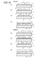
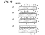
- the steps a1, b1, c1, and d1 of FIG. 1A correspond to the first manufacturing step of the semiconductor device using the substrate in the initial state that is not used for manufacturing the semiconductor device. Further, steps a2, b2, c2, and d2 in FIG. 1A show a substrate reuse step, and a substrate used at least once for manufacturing a semiconductor element was used. In addition, steps a3, b3, c3, and d3 of FIG. 1B show a further substrate reuse step. The steps a2 to d3 correspond to the second and subsequent manufacturing steps of the semiconductor element.
- step a1 shows a first mask forming step
- step a2 shows a second mask forming step
- Step b1 indicates a first element forming step
- step b2 indicates a second element forming step
- step c1 indicates a first mask removing step
- step c2 indicates a second mask removing step
- Step d1 indicates a first element separation step
- step d2 indicates a second element separation step.
- the substrate 1 commonly used in each process is prepared before the process a1.
- the substrate 1 has one main surface (hereinafter, also referred to as the first surface) 1a, which is the starting point of semiconductor crystal growth, and the other main surface (hereinafter, also referred to as the second surface) located on the opposite side of the first surface 1a. ) 1b and.
- the surface layer of the substrate 1 including the first surface 1a is made of a nitride semiconductor.
- the substrate 1 used in the embodiment is, for example, a GaN substrate cut out from a gallium nitride (GaN) single crystal ingot.
- GaN gallium nitride
- the substrate 1 may be an n-type substrate in which impurities such as Si are doped in the nitride semiconductor, or may be a p-type substrate in which impurities such as Mg are doped in the nitride semiconductor.
- the impurity density in the substrate 1 is, for example, about 1 ⁇ 10 19 cm -3 or less.
- a Si substrate, a sapphire substrate, a SiC substrate, or the like may be used as the GaN substrate.
- the substrate 1 may be formed of the same type of material as the semiconductor layer 3 to be grown on the substrate 1, or may be formed of a different material.
- the GaN layer may be grown on the GaN substrate.
- the GaN layer may be grown on the Si substrate, the sapphire substrate, or the SiC substrate.
- the substrate 1 is not limited to a substrate whose surface layer is a GaN layer, and may be a substrate whose surface layer is composed of a GaN-based semiconductor.
- the second surface 1b of the substrate 1 located on the opposite side of the first surface 1a is formed by the alteration of the substrate 1 or the nitride semiconductor by the step described later.
- a protective layer 4 for suppressing decomposition may be formed.
- the protective layer 4 may contain, for example, aluminum oxide, alumina, or the like.
- the protective layer 4 may also be formed on the end surface 1c of the substrate 1 that connects the first surface 1a and the second surface 1b.
- the protective layer 4 is positioned on the second surface 1b of the substrate 1. As a result, deterioration of the second surface 1b of the substrate 1 can be reduced. As a result, the growth conditions of the semiconductor crystal can be stabilized and the mass productivity can be improved.
- the method for manufacturing a semiconductor element using the substrate 1 in the initial state mainly corresponds to the steps a1, b1, c1, d1 in FIG. 1A, and forms the first mask 21 on the first surface 1a of the substrate 1.
- the first mask forming step a1, the first element forming step b1 for forming the semiconductor layer 3 on the first surface 1a of the masked substrate 1, and the deposition suppression mask 2 (referred to as the first mask 21) are removed by etching.
- the first mask removing step c1 and the first element separating step d1 for separating the semiconductor layer 3 from the first surface 1a of the substrate 1 are included.
- a semiconductor crystal (semiconductor layer 3) is grown on the first surface 1a of the substrate 1 (GaN substrate) by using photolithography technology and etching technology.
- the deposition suppression mask 2 (first mask 21) to be suppressed is formed in a predetermined pattern.
- the first mask 21 is formed so that the first region R1 which is a part of the first surface 1a of the substrate 1 is exposed.
- the semiconductor layer 3 can be formed in the first region R1 in a later step.
- the first mask 21 is first formed on the entire surface of the first surface 1a.
- the first mask 21 may be, for example, a silicon oxide (SiO 2 ) layer.
- silicon oxide is laminated on the first surface 1a by about 30 to 500 nm by using a PCVD (Plasma Chemical Vapor Deposition) method or the like.
- a photoresist is applied to the surface of the first mask 21 formed on the entire surface of the first surface 1a, which is opposite to the surface facing the first surface 1a (the surface on the front side of the first mask 21), and the resist is applied. Form a layer (not shown).
- the photoresist may be a positive photoresist or a negative photoresist.
- the photomask may be, for example, a glass substrate on which a mask pattern is drawn with chromium (Cr), titanium (Ti), tungsten (W), or the like.
- the exposed and developed resist layer is cured, unnecessary parts of the first mask 21 that are not covered by the resist layer are subjected to HF (hydrofluoric acid) -based wet etching or a fluorine-based gas such as CF 4. Removed by dry etching with. Subsequently, by removing the resist layer, the first mask 21 having a predetermined pattern can be formed on the first surface 1a of the substrate 1.
- the resist layer can be removed by using a known method such as lift-off with a solvent and ashing.
- the exposed surface E1 seen from the region (upward opening) from which the first mask 21 has been removed by etching is the first region R1 where the first surface 1a is exposed, and the first region R1 is the first element forming step b1. This is the region that is the starting point for the growth of semiconductor crystals.
- the first region R1 is formed in a plurality of strips, for example.
- the opening width or groove width which is the width (width of one of the plurality of bands) in the parallel direction (horizontal direction in FIG. 1A) of the exposed surface E1, may be, for example, 2 to 20 ⁇ m. Further, the width of the first mask 21 in the parallel direction in the embodiment is set to, for example, 150 to 200 ⁇ m.
- the relationship between the width of the first mask 21 in the parallel direction and the width of the exposed surface E1 in the parallel direction is the first surface 1a of the substrate 1 of the semiconductor layer 3 formed in the subsequent first element forming step b1.
- the ratio of the crystal growth rate in the direction perpendicular to the above to the crystal growth rate in the direction parallel to the first surface 1a of the substrate 1 and the thickness of the semiconductor layer 3 to be grown may be taken into consideration.
- the pattern of the first mask 21 may be a band shape or a stripe shape, or a grid shape in which a plurality of band shapes are arranged so as to be orthogonal to each other in the vertical and horizontal directions. Any pattern may be used as long as it is a so-called repeat pattern in which openings divided at regular intervals (repeat pitch) are repeated a plurality of times.
- edge region 1e on the first surface 1a near the end surface 1c may also be covered with the first mask 21. This facilitates the separation of the semiconductor layer 3 in the subsequent first element separation step d1, and the semiconductor layer 3 located at the edge of the substrate 1 near the edge can also be separated neatly.
- the mask material constituting the first mask 21 for example, a material containing silicon oxide such as SiO 2 is used.
- the deposition suppression mask 2 may be any material as long as the semiconductor layer does not grow from the surface of the mask material due to vapor phase growth. Outside those containing silicon oxide, for example, zirconium oxide (ZrO X), titanium oxide (TiO X), it is possible to use an oxide such as aluminum oxide (AlO X).
- a transition metal selected from chromium (Cr), tungsten (W), molybdenum (Mo), tantalum (Ta), niobium (Nb) and the like may be used.
- a method for depositing the mask material a method suitable for the mask material such as thin film deposition, sputtering, and coating curing can be appropriately used.
- the semiconductor crystal is epitaxially grown (Epitaxial Lateral Overgrowth; ELO) so as to spread from the exposed surface E1 which is the first region R1 to the adjacent first mask 21.
- the semiconductor layer 3 (also referred to as the first semiconductor layer 31) forming a part of the element is formed.
- the semiconductor layer 3 in the embodiment is a nitride semiconductor, and by epitaxial growth, the nitride semiconductor is spread from the first surface 1a to the upper surface of the first mask 21 beyond the upper edge opening of the groove of the first mask 21. Grow.
- a vapor phase growth method such as the Metalorganic Chemical Vapor Deposition (MOCVD) method or the Molecular Beam Epitaxy (MBE) method can be used.
- the substrate 1 on which the first mask 21 is patterned is inserted into the reaction chamber of the epitaxial apparatus, and hydrogen gas, nitrogen gas, or hydrogen is used. While supplying a mixed gas of hydrogen and nitrogen and a group V raw material (containing a group 15 element) gas such as ammonia, the substrate 1 is heated to a predetermined growth temperature, for example, 1050 to 1100 ° C.
- a group III (group 13 element-containing) raw material such as trimethylgallium (TMG) is supplied to grow crystals.
- TMG trimethylgallium
- the semiconductor layer 3 is epitaxially grown from the exposed surface E1 which is a region (first region R1).
- a desired conductive type GaN layer can be obtained by supplying a raw material gas such as an n-type impurity such as Si or a p-type impurity such as Mg and adjusting the doping amount. Further, the supply of the raw material may be temporarily stopped to stop the growth of the semiconductor crystal before the growth crystal crosses the edge of the opening of the groove between the first masks 21 or the growth crystal fills the groove. In this way, the "fragile portion" that facilitates the separation of the semiconductor layer 3 in the first element separation step d1 may be formed as a partial layer or film before restarting the supply of the raw material.
- the fragile portion for example, when the GaN layer is crystal-grown, the upper portion of the semiconductor layer 3 located on the opening side in the groove of the first region R1 and the lower portion of the semiconductor layer 3 located on the exposed surface E1 side. In between, a layer made of a mixed crystal of GaN and BN, AlN, InN, etc. may be formed as a fragile portion.
- the semiconductor layer 3 may be formed.
- a fragile portion having a superlattice structure may be formed by alternately stacking AlGaN layers and GaN layers.
- the fragile portion may be formed by alternately laminating large layers of GaN crystal grains and small layers of crystal grains by periodically changing the crystal growth conditions.
- the fragile portion may be a layer in which the impurity concentration is changed by changing the concentration of silicon (Si) used as an n-type impurity of GaN.
- GaN When a fragile portion is formed, GaN is continuously vapor-deposited starting from the upper surface (surface) of the fragile portion. When the fragile portion is not formed, GaN is vapor-deposited starting from the exposed surface E1 between the first regions R1.
- the semiconductor layer 3 grows in the lateral direction (horizontal direction in FIG. 1A) along the upper surface of the deposition suppression mask 2. Therefore, through dislocations of the semiconductor layer 3 can be reduced.
- the first element forming step b1 is completed before each semiconductor layer 3 that has started to grow from the exposed surface E1 of the first region R1 comes into contact with or overlaps with the adjacent first semiconductor layer 31. As a result, it is possible to reduce crystal defects such as cracks or through dislocations that may occur when adjacent semiconductor layers 3 are in contact with each other.
- the semiconductor element in the first element forming step b1, at least a part of the semiconductor element may be formed, and not all the configurations of the semiconductor element may be formed before c1 before the first mask removing step. Further, when all the configurations of the semiconductor element are not formed, the remaining configurations of the semiconductor element may be formed after the first mask removing step c1 or after the first element separation step d1. Further, the configuration of the semiconductor element may be appropriately formed according to the type of the semiconductor element.
- the first semiconductor layer 31 has a substantially T-shaped shape connected to the substrate 1 by a thin connecting portion located on the exposed surface E1. As a result, the first semiconductor layer 31 can be smoothly separated.
- a member or jig such as a support substrate 6 having an adhesive layer 5 made of solder using a material such as AuSn is formed on one surface (lower surface).
- This is a step of separating at least a part (for example, the first semiconductor layer 31) of the semiconductor element formed in the first element forming step b1 from the substrate 1 and forming each into an individual semiconductor element S.
- the support substrate 6 having the adhesive layer 5 on the lower surface is opposed to the surface (first surface 1a) on which the first semiconductor layer 31 of the substrate 1 is formed. Subsequently, the support substrate 6 is pressed toward the substrate 1 and the adhesive layer 5 is heated to bond the semiconductor 3 to the adhesive layer 5.
- the first element separation step d1 may include a step of dividing the first semiconductor layer 31 according to the size of the semiconductor element S, and a step of forming an electrode, a wiring conductor, or the like on the first semiconductor layer 31.
- the first semiconductor layer 31 may be divided by cleavage on the cleavage plane.
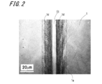
- FIG. 2 schematically shows a region (hereinafter, also referred to as a defect region) 1d in which a pit and a transition defect have occurred.
- FIG. 2 shows a state in which a transition defect is generated on the first surface 1a of the substrate 1.
- the method for manufacturing a semiconductor element according to the present invention includes a substrate reuse step of growing a semiconductor crystal (second semiconductor layer 32) again from a second region R2 that at least partially overlaps with the first region R1. There is.
- the second region R2 and the first region R1 are substantially coincident regions.
- the substrate reuse step includes a second substrate reuse step having “step a2” to “step d2”.
- “Step a2” indicates the second mask forming step a2
- “step b2” indicates the second element forming step b2
- “step c2” indicates the second mask removing step c2
- “step d2” indicates the second element.
- the separation step d2 is shown.
- the second substrate reuse step is carried out in a state where the first surface 1a exposed after the first element separation step d1 described above is not polished.
- at least a part of the first surface 1a is subjected to deposits adhering to the first surface 1a. It may be performed after the cleaning step of cleaning.
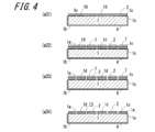
- (A2) Second Mask Forming Step In the second mask forming step a2, a photolithography technique and an etching technique are used to create a new area including the forming position of the first mask 21 formed in the first mask forming step a1.
- the deposition suppression mask 2 (also referred to as the second mask 22) is formed to expose the exposed surface (also referred to as the second crystal growth region (second region R2)) E2 not covered by the second mask 22.
- the second mask forming step a2 is composed of the first step to the fourth step.
- “step a21" indicates the first step
- step a22" indicates the second step
- step a23" indicates the third step
- step a24 indicates the fourth step.
- a deposition suppression mask 2 (second mask 22) is formed on the entire surface of the first surface 1a of the substrate 1.
- the second mask 22 may be, for example, a silicon oxide (SiO 2 ) layer having a thickness of about 30 to 500 nm.
- silicon oxide is laminated on the first surface 1a by about 30 to 500 nm by using a PCVD method or the like.
- (A22) Second Step In the second step a22, first, on the surface of the second mask 22 formed in the first step a21 opposite to the surface facing the substrate 1 (the surface on the front side of the second mask 22). A photoresist is applied to form the resist layer 7.
- the photoresist may be a positive photoresist or a negative photoresist.
- a photomask (not shown) on which a mask pattern corresponding to the mask pattern of the photomask used in the first mask forming step a1 is drawn is prepared.
- the photomask is, for example, a glass substrate on which a mask pattern is drawn with chromium (Cr), titanium (Ti), tungsten (W), or the like.
- the prepared photomask is positioned on the substrate 1 at a predetermined position in the same manner as in the first mask forming step a1, and then the pattern drawn on the photomask is exposed and developed on the resist layer.
- the photomask may be positioned with respect to the substrate 1 based on the outer shape of the substrate 1 and the photomask, the mask pattern drawn on the photomask, the position of the defect region 1d, and the like. Alignment marks for alignment are formed on the substrate 1 and the photomask, and in the first mask forming step a1 and the second mask forming step a2, the photomask is positioned with respect to the substrate 1 based on the alignment marks. May be good.
- the resist layer 7 is removed by using a known method such as lift-off with a solvent and ashing to expose the exposed surface E2 which at least partially overlaps the exposed surface E1.
- the second region R2 which at least partially overlaps the first region R1, can be exposed on the first surface 1a of the substrate 1.
- the second region R2 may be included in the first region R1 and does not have to completely coincide with the first region R1. Further, the second region R2 may include the defect region 1d as long as the normal semiconductor crystal can grow. The second region R2 may be smaller than the first region R1.
- the second mask 22 may be formed also in the edge region 1e of the first surface 1a.
- the semiconductor layer 3 can be easily separated in the second element separation step d2, and the semiconductor layer 3 existing in the vicinity of the edge portion located at the end of the substrate 1 can also be separated neatly.
- a semiconductor crystal is grown from the exposed surface E2, which is the second region R2, so as to spread over the upper surface of the adjacent second mask 22, and a part of the element is grown.
- the constituent semiconductor layer 3 (also referred to as the second semiconductor layer 32) is formed.
- the second element forming step b2 may be the same as the first element forming step b1.
- (C2) Second Mask Removal Step After the completion of the second element forming step b2, the second mask 22 is removed using an etchant that does not substantially invade the grown second semiconductor layer 32.
- the second mask removing step c2 may be the same as the first mask removing step c1.
- the second element separation step d2 is a step of separating the second semiconductor layer 32 from the substrate 1 and forming each into individual semiconductor elements S.
- the second element separation step d2 may be the same as the first element separation step d1.
- the first surface 1a of the substrate 1 is regenerated without removing pits and transition defects by polishing or the like. It can be used to form a second semiconductor device. This makes it possible to reduce the number of steps in the manufacture of semiconductor devices and improve productivity.
- the second substrate reuse step may be repeated twice or more.
- the method for manufacturing a semiconductor element of the embodiment it is possible to reduce a large decrease in the thickness of the substrate 1 due to polishing or the like.
- the substrate reuse step may further include a third substrate reuse step having "steps a3" to "step d3".
- “Step a3” indicates the third mask forming step a3
- “step b3” indicates the third element forming step b3
- “step c3” indicates the third mask removing step c3
- “step d3” indicates the third element.
- the separation step d3 is shown.
- (A3) Third Mask Forming Step In the third mask forming step a3, a new area including the forming position of the second mask 22 formed in the second mask forming step a2 is created by using the photolithography technique and the etching technique.
- the deposition suppression mask 2 (third mask 23) is formed to expose the exposed surface (also referred to as the third crystal growth region (third region R3)) E3 not covered by the third mask 23.
- the third mask forming step a3 is composed of the first step to the fourth step.
- “step a31” indicates the first step
- step a32” indicates the second step
- step a33” indicates the third step
- step a34” indicates the fourth step.
- the third mask forming step a3 may be performed after polishing the first surface 1a exposed after the second element separation step d2 described above, or may be performed without polishing. May be done. Even if polishing is performed before the third mask forming step a3, since the second mask removing step is interposed, the substrate 1 is consumed less than the case where the substrate 1 is polished for each element separation step. Can be reduced. Further, the third mask forming step a3 may be performed after the plurality of second substrate reuse steps. The second substrate reuse step and the third substrate reuse step may be performed a plurality of times, respectively, and the number of times of the second substrate reuse step may be larger than the number of times of the third substrate reuse step. ..
- a deposition suppression mask 2 (also referred to as a third mask 23) is formed on the entire surface of the first surface 1a of the substrate 1.
- the third mask 23 may be, for example, a silicon oxide (SiO 2 ) layer having a thickness of about 30 to 500 nm.
- silicon oxide is laminated on the first surface 1a by about 30 to 500 nm by using a PCVD method or the like.
- (A32) Second Step In the second step a32, first, on the surface of the third mask 23 formed in the first step a31 opposite to the surface facing the substrate 1 (the surface on the front side of the third mask 23). A photoresist is applied to form a resist layer 7.
- the photoresist may be a positive photoresist or a negative photoresist.
- a photomask (not shown) on which a mask pattern corresponding to the mask pattern of the photomask used in the second mask forming step a2 is drawn is prepared.
- the photomask is, for example, a glass substrate on which a mask pattern is drawn with chromium (Cr), titanium (Ti), tungsten (W), or the like.
- the prepared photomask is positioned on the substrate 1 at a predetermined position in the same manner as in the second mask forming step a2, and then the pattern drawn on the photomask is exposed and developed on the resist layer.
- the photomask may be positioned with respect to the substrate 1 based on the outer shape of the substrate 1 and the photomask, the mask pattern drawn on the photomask, the position of the defect region 1d, and the like. Alignment marks for alignment are formed on the substrate 1 and the photomask, and in the second mask forming step a2 and the third mask forming step a3, the photomask is positioned with respect to the substrate 1 based on the alignment marks. May be good.
- the resist layer 7 is removed by using a known method such as lift-off with a solvent and ashing to expose the exposed surface E3 which at least partially overlaps the exposed surface E2.
- the third region R3, which at least partially overlaps the second region R2, can be exposed on the first surface 1a of the substrate 1.
- the third region R3 need only be included in the second region R2, and does not have to completely coincide with the second region R2.
- the third region R3 may include the defect region 1d as long as the normal semiconductor crystal can grow. At least a part of the third region R3 may overlap with the first region R1. Further, the third region R3 may be separated from the first region R1. Further, the third region R3 may be smaller than the first region R1.
- the third mask 23 may be formed also in the edge region 1e of the first surface 1a.
- the semiconductor layer 3 can be easily separated in the third element separation step d3, and the semiconductor layer 3 existing in the vicinity of the edge portion located at the end of the substrate 1 can also be separated neatly.
- (B3) Third Element Forming Step In the third element forming step b3, a semiconductor crystal is grown from the exposed surface E3, which is the third region R3, so as to spread over the upper surface of the adjacent third mask 23, and a part of the element is formed.
- the constituent semiconductor layer 3 also referred to as the third semiconductor layer 33
- the third element forming step b3 may be the same as the second element forming step b2.
- (C3) Third Mask Removal Step After the completion of the third element forming step b3, the third mask 23 is removed using an etchant that does not substantially invade the grown third semiconductor layer 33.
- the third mask removing step c3 may be the same as the second mask removing step c2.
- the third element separation step d3 is a step of separating the third semiconductor layer 33 from the substrate 1 and forming each into individual semiconductor elements S.
- the third element separation step d3 may be the same as the second element separation step d2.
- the first surface 1a of the substrate 1 is reused without removing pits and transition defects by polishing or the like. can do. This makes it possible to reduce the number of steps in the manufacture of semiconductor devices and improve productivity.
- the productivity of the semiconductor element can be improved.
- the thickness of the substrate 1 after the second element or the third element is peeled off after the second substrate reuse step (second element separation step d2) or the third substrate reuse step (third element separation step d3). It may be further provided with a substrate growth step for increasing the size.
- the substrate 1 itself can be regenerated, and the semiconductor element can be manufactured again.
- the substrate 1 itself may be regenerated in the same manner as, for example, a single crystal ingot. Specifically, for example, it may be carried out by vapor phase growth or liquid phase growth.
- the second substrate reuse step is carried out after the first element separation step d1 without polishing the first surface 1a, but after the first element separation step d1, the second element is described.
- the first surface 1a may be polished before the forming step b2.
- the separation of the first element may be performed together with a part of the surface layer of the substrate 1 with which the first element is in contact.
- a part of the surface layer of the substrate 1 can be removed, and the surface of the substrate 1 having few defects can be newly exposed.
- steps such as polishing the entire first surface a can be skipped, and the productivity of the semiconductor element can be improved.
- the substrate 1 may be peeled off so as to apply stress.
- the first element may be separated after removing the region including the portion of the first semiconductor layer 31 in contact with the substrate 1. That is, the first semiconductor layer 31 located on the first mask is used as the first element (or a part of the first element), and after removing the other parts, the first element (or a part of the first element). May be separated using the adhesive layer 5 and the support substrate 6. At this time, the first mask may be removed after the adhesive layer 5 and the support substrate 6 are adhered to the first semiconductor layer 31. If the first mask is removed, the first element can be easily separated from the substrate 1.
- a material to which the material of the semiconductor layer 3 does not easily adhere can be used.
- a fluororesin layer can be used. It may be.
- the deposition suppression mask 2 may be treated with fluorine on the surface of a layer made of an inorganic or organic material.
- the deposition suppression mask 2 directly performs fluorine treatment on the first main surface a of the substrate 1 except for the first region R1, the second region R2 or the third region R3 to suppress the deposition. It may function as a mask 2. By using a fluorine-based material, the growth of the semiconductor layer 3 can be reduced.
- the first mask 21 is removed before separating the first element has been described, but the first mask 21 is not removed and is reused as the second mask 22 or the third mask 23. May be good.
- the semiconductor device manufacturing method of the present disclosure includes a process of preparing a substrate and A first element forming step of forming a first semiconductor layer in a first region on the surface of the substrate, and A first element separation step of separating the first semiconductor layer from the substrate, and A second element forming step of forming the second semiconductor layer in the second region of the surface of the substrate from which the first semiconductor layer is separated, and With At least a part of the second region is configured to overlap the first region.
- the productivity of the semiconductor device can be improved by reducing the number of steps in manufacturing the semiconductor device and improving the quality of the semiconductor device.
Landscapes
- Engineering & Computer Science (AREA)
- Chemical & Material Sciences (AREA)
- Manufacturing & Machinery (AREA)
- Computer Hardware Design (AREA)
- Microelectronics & Electronic Packaging (AREA)
- Power Engineering (AREA)
- General Physics & Mathematics (AREA)
- Physics & Mathematics (AREA)
- Condensed Matter Physics & Semiconductors (AREA)
- Materials Engineering (AREA)
- Crystallography & Structural Chemistry (AREA)
- Metallurgy (AREA)
- Organic Chemistry (AREA)
- General Chemical & Material Sciences (AREA)
- Chemical Kinetics & Catalysis (AREA)
- Inorganic Chemistry (AREA)
- Recrystallisation Techniques (AREA)
Abstract
Un procédé de fabrication d'un élément semi-conducteur selon la présente divulgation comprend une étape de préparation d'un substrat, une étape de formation d'un premier élément consistant à former une première couche de semi-conducteur dans une première région sur la surface du substrat, une étape de séparation du premier élément consistant à séparer la première couche de semi-conducteur du substrat, et une étape de formation de second élément consistant à former une seconde couche de semi-conducteur dans une seconde région sur la surface du substrat à partir duquel la première couche de semi-conducteur a été séparée. Dans ce procédé de fabrication d'un élément semi-conducteur, au moins une partie de la seconde région chevauche la première région.
Priority Applications (2)
| Application Number | Priority Date | Filing Date | Title |
|---|---|---|---|
| US17/764,430 US20220376132A1 (en) | 2019-09-30 | 2020-09-30 | Method for manufacturing semiconductor element |
| JP2021551397A JPWO2021066042A1 (fr) | 2019-09-30 | 2020-09-30 |
Applications Claiming Priority (2)
| Application Number | Priority Date | Filing Date | Title |
|---|---|---|---|
| JP2019179582 | 2019-09-30 | ||
| JP2019-179582 | 2019-09-30 |
Publications (1)
| Publication Number | Publication Date |
|---|---|
| WO2021066042A1 true WO2021066042A1 (fr) | 2021-04-08 |
Family
ID=75337015
Family Applications (1)
| Application Number | Title | Priority Date | Filing Date |
|---|---|---|---|
| PCT/JP2020/037240 WO2021066042A1 (fr) | 2019-09-30 | 2020-09-30 | Procédé de fabrication d'élément semi-conducteur |
Country Status (3)
| Country | Link |
|---|---|
| US (1) | US20220376132A1 (fr) |
| JP (1) | JPWO2021066042A1 (fr) |
| WO (1) | WO2021066042A1 (fr) |
Citations (7)
| Publication number | Priority date | Publication date | Assignee | Title |
|---|---|---|---|---|
| JPH09306848A (ja) * | 1996-05-16 | 1997-11-28 | Nec Corp | 半導体結晶性膜の成長方法 |
| JP2003007616A (ja) * | 2001-03-23 | 2003-01-10 | Matsushita Electric Ind Co Ltd | 半導体膜の製造方法 |
| JP2007073569A (ja) * | 2005-09-05 | 2007-03-22 | Sumitomo Electric Ind Ltd | 窒化物半導体デバイスの製造方法および窒化物半導体デバイス |
| JP2013251304A (ja) * | 2012-05-30 | 2013-12-12 | Furukawa Co Ltd | 積層体および積層体の製造方法 |
| JP2014225554A (ja) * | 2013-05-16 | 2014-12-04 | 株式会社新菱 | 再生基板の製造方法 |
| WO2017164233A1 (fr) * | 2016-03-23 | 2017-09-28 | 株式会社トクヤマ | Procédé de fabrication d'un substrat de cristal unique de nitrure d'aluminium |
| JP2019134101A (ja) * | 2018-01-31 | 2019-08-08 | 京セラ株式会社 | 半導体素子の製造方法 |
-
2020
- 2020-09-30 WO PCT/JP2020/037240 patent/WO2021066042A1/fr active Application Filing
- 2020-09-30 JP JP2021551397A patent/JPWO2021066042A1/ja active Pending
- 2020-09-30 US US17/764,430 patent/US20220376132A1/en active Pending
Patent Citations (7)
| Publication number | Priority date | Publication date | Assignee | Title |
|---|---|---|---|---|
| JPH09306848A (ja) * | 1996-05-16 | 1997-11-28 | Nec Corp | 半導体結晶性膜の成長方法 |
| JP2003007616A (ja) * | 2001-03-23 | 2003-01-10 | Matsushita Electric Ind Co Ltd | 半導体膜の製造方法 |
| JP2007073569A (ja) * | 2005-09-05 | 2007-03-22 | Sumitomo Electric Ind Ltd | 窒化物半導体デバイスの製造方法および窒化物半導体デバイス |
| JP2013251304A (ja) * | 2012-05-30 | 2013-12-12 | Furukawa Co Ltd | 積層体および積層体の製造方法 |
| JP2014225554A (ja) * | 2013-05-16 | 2014-12-04 | 株式会社新菱 | 再生基板の製造方法 |
| WO2017164233A1 (fr) * | 2016-03-23 | 2017-09-28 | 株式会社トクヤマ | Procédé de fabrication d'un substrat de cristal unique de nitrure d'aluminium |
| JP2019134101A (ja) * | 2018-01-31 | 2019-08-08 | 京セラ株式会社 | 半導体素子の製造方法 |
Also Published As
| Publication number | Publication date |
|---|---|
| US20220376132A1 (en) | 2022-11-24 |
| JPWO2021066042A1 (fr) | 2021-04-08 |
Similar Documents
| Publication | Publication Date | Title |
|---|---|---|
| JP4741572B2 (ja) | 窒化物半導体基板及びその製造方法 | |
| CN111095483B (zh) | 利用切割技术移除衬底的方法 | |
| JP5371430B2 (ja) | 半導体基板並びにハイドライド気相成長法により自立半導体基板を製造するための方法及びそれに使用されるマスク層 | |
| US20030155586A1 (en) | Methods and devices using group III nitride compound semiconductor | |
| US9425347B2 (en) | Semiconductor substrate, semiconductor device, and manufacturing methods thereof | |
| US10615032B2 (en) | Semiconductor device manufacturing method | |
| JP2020519026A (ja) | 基板を除去する方法 | |
| JP2019131441A (ja) | 結晶成長方法および半導体素子の製造方法 | |
| US10600645B2 (en) | Manufacturing method of gallium nitride substrate | |
| CN116249803A (zh) | 紫外线发光元件用外延晶圆、紫外线发光元件用金属贴合基板的制造方法、紫外线发光元件的制造方法、及紫外线发光元件阵列的制造方法 | |
| US20070298592A1 (en) | Method for manufacturing single crystalline gallium nitride material substrate | |
| JP2023162378A (ja) | 半導体素子 | |
| WO2021066042A1 (fr) | Procédé de fabrication d'élément semi-conducteur | |
| JP2023139075A (ja) | 半導体デバイスの製造方法および半導体デバイス並びにテンプレート基板 | |
| JP7221302B2 (ja) | 半導体素子の製造方法、半導体素子および半導体デバイス | |
| JP7221431B2 (ja) | 複数の半導体素子の製造方法 | |
| JP2010180114A (ja) | GaN系化合物半導体の成長方法及び成長層付き基板 | |
| JP2021145052A (ja) | 半導体素子の製造方法 | |
| JP2009231378A (ja) | デバイスの製造方法 | |
| JP7378239B2 (ja) | 積層体、窒化物半導体層の製造方法 | |
| JP2014005189A (ja) | 周期表第13族金属窒化物半導体基板の製造方法 | |
| JP2013209271A (ja) | 周期表第13族金属窒化物半導体基板の製造方法、および、当該製造方法に用いられる下地基板 | |
| JP5225133B2 (ja) | GaN系化合物半導体の成長方法及び成長層付き基板 | |
| KR20110037086A (ko) | 질화물 반도체 결정 성장 방법 | |
| JP2002217113A (ja) | 窒化物半導体層の製造方法および窒化物半導体基板の製造方法ならびに窒化物半導体基板製造用基体 |
Legal Events
| Date | Code | Title | Description |
|---|---|---|---|
| 121 | Ep: the epo has been informed by wipo that ep was designated in this application |
Ref document number: 20872058 Country of ref document: EP Kind code of ref document: A1 |
|
| ENP | Entry into the national phase |
Ref document number: 2021551397 Country of ref document: JP Kind code of ref document: A |
|
| NENP | Non-entry into the national phase |
Ref country code: DE |
|
| 122 | Ep: pct application non-entry in european phase |
Ref document number: 20872058 Country of ref document: EP Kind code of ref document: A1 |