WO2021066042A1 - Method for manufacturing semiconductor element - Google Patents
Method for manufacturing semiconductor element Download PDFInfo
- Publication number
- WO2021066042A1 WO2021066042A1 PCT/JP2020/037240 JP2020037240W WO2021066042A1 WO 2021066042 A1 WO2021066042 A1 WO 2021066042A1 JP 2020037240 W JP2020037240 W JP 2020037240W WO 2021066042 A1 WO2021066042 A1 WO 2021066042A1
- Authority
- WO
- WIPO (PCT)
- Prior art keywords
- substrate
- manufacturing
- mask
- semiconductor device
- region
- Prior art date
Links
Images

Classifications
-
- H—ELECTRICITY
- H01—ELECTRIC ELEMENTS
- H01L—SEMICONDUCTOR DEVICES NOT COVERED BY CLASS H10
- H01L21/00—Processes or apparatus adapted for the manufacture or treatment of semiconductor or solid state devices or of parts thereof
- H01L21/70—Manufacture or treatment of devices consisting of a plurality of solid state components formed in or on a common substrate or of parts thereof; Manufacture of integrated circuit devices or of parts thereof
- H01L21/77—Manufacture or treatment of devices consisting of a plurality of solid state components or integrated circuits formed in, or on, a common substrate
- H01L21/78—Manufacture or treatment of devices consisting of a plurality of solid state components or integrated circuits formed in, or on, a common substrate with subsequent division of the substrate into plural individual devices
- H01L21/7806—Manufacture or treatment of devices consisting of a plurality of solid state components or integrated circuits formed in, or on, a common substrate with subsequent division of the substrate into plural individual devices involving the separation of the active layers from a substrate
- H01L21/7813—Manufacture or treatment of devices consisting of a plurality of solid state components or integrated circuits formed in, or on, a common substrate with subsequent division of the substrate into plural individual devices involving the separation of the active layers from a substrate leaving a reusable substrate, e.g. epitaxial lift off
-
- C—CHEMISTRY; METALLURGY
- C30—CRYSTAL GROWTH
- C30B—SINGLE-CRYSTAL GROWTH; UNIDIRECTIONAL SOLIDIFICATION OF EUTECTIC MATERIAL OR UNIDIRECTIONAL DEMIXING OF EUTECTOID MATERIAL; REFINING BY ZONE-MELTING OF MATERIAL; PRODUCTION OF A HOMOGENEOUS POLYCRYSTALLINE MATERIAL WITH DEFINED STRUCTURE; SINGLE CRYSTALS OR HOMOGENEOUS POLYCRYSTALLINE MATERIAL WITH DEFINED STRUCTURE; AFTER-TREATMENT OF SINGLE CRYSTALS OR A HOMOGENEOUS POLYCRYSTALLINE MATERIAL WITH DEFINED STRUCTURE; APPARATUS THEREFOR
- C30B25/00—Single-crystal growth by chemical reaction of reactive gases, e.g. chemical vapour-deposition growth
- C30B25/02—Epitaxial-layer growth
- C30B25/04—Pattern deposit, e.g. by using masks
-
- C—CHEMISTRY; METALLURGY
- C30—CRYSTAL GROWTH
- C30B—SINGLE-CRYSTAL GROWTH; UNIDIRECTIONAL SOLIDIFICATION OF EUTECTIC MATERIAL OR UNIDIRECTIONAL DEMIXING OF EUTECTOID MATERIAL; REFINING BY ZONE-MELTING OF MATERIAL; PRODUCTION OF A HOMOGENEOUS POLYCRYSTALLINE MATERIAL WITH DEFINED STRUCTURE; SINGLE CRYSTALS OR HOMOGENEOUS POLYCRYSTALLINE MATERIAL WITH DEFINED STRUCTURE; AFTER-TREATMENT OF SINGLE CRYSTALS OR A HOMOGENEOUS POLYCRYSTALLINE MATERIAL WITH DEFINED STRUCTURE; APPARATUS THEREFOR
- C30B25/00—Single-crystal growth by chemical reaction of reactive gases, e.g. chemical vapour-deposition growth
- C30B25/02—Epitaxial-layer growth
- C30B25/18—Epitaxial-layer growth characterised by the substrate
- C30B25/183—Epitaxial-layer growth characterised by the substrate being provided with a buffer layer, e.g. a lattice matching layer
-
- C—CHEMISTRY; METALLURGY
- C30—CRYSTAL GROWTH
- C30B—SINGLE-CRYSTAL GROWTH; UNIDIRECTIONAL SOLIDIFICATION OF EUTECTIC MATERIAL OR UNIDIRECTIONAL DEMIXING OF EUTECTOID MATERIAL; REFINING BY ZONE-MELTING OF MATERIAL; PRODUCTION OF A HOMOGENEOUS POLYCRYSTALLINE MATERIAL WITH DEFINED STRUCTURE; SINGLE CRYSTALS OR HOMOGENEOUS POLYCRYSTALLINE MATERIAL WITH DEFINED STRUCTURE; AFTER-TREATMENT OF SINGLE CRYSTALS OR A HOMOGENEOUS POLYCRYSTALLINE MATERIAL WITH DEFINED STRUCTURE; APPARATUS THEREFOR
- C30B29/00—Single crystals or homogeneous polycrystalline material with defined structure characterised by the material or by their shape
- C30B29/10—Inorganic compounds or compositions
- C30B29/40—AIIIBV compounds wherein A is B, Al, Ga, In or Tl and B is N, P, As, Sb or Bi
- C30B29/403—AIII-nitrides
- C30B29/406—Gallium nitride
-
- H—ELECTRICITY
- H01—ELECTRIC ELEMENTS
- H01L—SEMICONDUCTOR DEVICES NOT COVERED BY CLASS H10
- H01L21/00—Processes or apparatus adapted for the manufacture or treatment of semiconductor or solid state devices or of parts thereof
- H01L21/02—Manufacture or treatment of semiconductor devices or of parts thereof
- H01L21/02041—Cleaning
- H01L21/02043—Cleaning before device manufacture, i.e. Begin-Of-Line process
-
- H—ELECTRICITY
- H01—ELECTRIC ELEMENTS
- H01L—SEMICONDUCTOR DEVICES NOT COVERED BY CLASS H10
- H01L21/00—Processes or apparatus adapted for the manufacture or treatment of semiconductor or solid state devices or of parts thereof
- H01L21/02—Manufacture or treatment of semiconductor devices or of parts thereof
- H01L21/02104—Forming layers
- H01L21/02365—Forming inorganic semiconducting materials on a substrate
- H01L21/02518—Deposited layers
- H01L21/02521—Materials
- H01L21/02538—Group 13/15 materials
- H01L21/0254—Nitrides
-
- H—ELECTRICITY
- H01—ELECTRIC ELEMENTS
- H01L—SEMICONDUCTOR DEVICES NOT COVERED BY CLASS H10
- H01L21/00—Processes or apparatus adapted for the manufacture or treatment of semiconductor or solid state devices or of parts thereof
- H01L21/02—Manufacture or treatment of semiconductor devices or of parts thereof
- H01L21/02104—Forming layers
- H01L21/02365—Forming inorganic semiconducting materials on a substrate
- H01L21/02612—Formation types
- H01L21/02617—Deposition types
- H01L21/02636—Selective deposition, e.g. simultaneous growth of mono- and non-monocrystalline semiconductor materials
- H01L21/02639—Preparation of substrate for selective deposition
-
- H—ELECTRICITY
- H01—ELECTRIC ELEMENTS
- H01L—SEMICONDUCTOR DEVICES NOT COVERED BY CLASS H10
- H01L21/00—Processes or apparatus adapted for the manufacture or treatment of semiconductor or solid state devices or of parts thereof
- H01L21/02—Manufacture or treatment of semiconductor devices or of parts thereof
- H01L21/02104—Forming layers
- H01L21/02365—Forming inorganic semiconducting materials on a substrate
- H01L21/02612—Formation types
- H01L21/02617—Deposition types
- H01L21/02636—Selective deposition, e.g. simultaneous growth of mono- and non-monocrystalline semiconductor materials
- H01L21/02647—Lateral overgrowth
-
- H—ELECTRICITY
- H01—ELECTRIC ELEMENTS
- H01L—SEMICONDUCTOR DEVICES NOT COVERED BY CLASS H10
- H01L21/00—Processes or apparatus adapted for the manufacture or treatment of semiconductor or solid state devices or of parts thereof
- H01L21/02—Manufacture or treatment of semiconductor devices or of parts thereof
- H01L21/04—Manufacture or treatment of semiconductor devices or of parts thereof the devices having at least one potential-jump barrier or surface barrier, e.g. PN junction, depletion layer or carrier concentration layer
- H01L21/18—Manufacture or treatment of semiconductor devices or of parts thereof the devices having at least one potential-jump barrier or surface barrier, e.g. PN junction, depletion layer or carrier concentration layer the devices having semiconductor bodies comprising elements of Group IV of the Periodic System or AIIIBV compounds with or without impurities, e.g. doping materials
- H01L21/30—Treatment of semiconductor bodies using processes or apparatus not provided for in groups H01L21/20 - H01L21/26
- H01L21/302—Treatment of semiconductor bodies using processes or apparatus not provided for in groups H01L21/20 - H01L21/26 to change their surface-physical characteristics or shape, e.g. etching, polishing, cutting
- H01L21/304—Mechanical treatment, e.g. grinding, polishing, cutting
-
- H—ELECTRICITY
- H01—ELECTRIC ELEMENTS
- H01L—SEMICONDUCTOR DEVICES NOT COVERED BY CLASS H10
- H01L33/00—Semiconductor devices with at least one potential-jump barrier or surface barrier specially adapted for light emission; Processes or apparatus specially adapted for the manufacture or treatment thereof or of parts thereof; Details thereof
- H01L33/005—Processes
- H01L33/0062—Processes for devices with an active region comprising only III-V compounds
- H01L33/0066—Processes for devices with an active region comprising only III-V compounds with a substrate not being a III-V compound
- H01L33/007—Processes for devices with an active region comprising only III-V compounds with a substrate not being a III-V compound comprising nitride compounds
Definitions
- This disclosure relates to a method for manufacturing a semiconductor device.
- Patent Document 1 An example of the prior art is described in Patent Document 1 and Patent Document 2.
- the semiconductor element manufacturing method of the present disclosure includes a step of preparing a substrate, a first element forming step of forming a first semiconductor layer in a first region on the surface of the substrate, and a step of separating the first semiconductor layer from the substrate.
- the first element separating step is provided, and the second element forming step of forming the second semiconductor layer in the second region on the surface of the substrate from which the first semiconductor layer is separated is provided.
- at least a part of the second region is overlapped with the first region.
- a method for manufacturing a semiconductor element a method is known in which a mask having an opening is formed on a substrate and then a semiconductor layer to be a semiconductor element is grown from an exposed surface exposed to the opening by using a transverse epitaxial growth method. (See, for example, Patent Documents 1 and 2).
- the grown semiconductor layer is transferred to a support substrate or the like and separated from the substrate.
- Patent Document 2 describes that a peeling step of peeling a GaN-based semiconductor layer, and after the peeling step, a mask forming step and a growing step are performed using the peeled GaN substrate.
- the present invention relates to a method for manufacturing a semiconductor device.
- the semiconductor element manufactured by the manufacturing method according to the present invention may be, for example, a light emitting element, a light receiving element, or a Schottky barrier diode.
- a light emitting element for example, a light emitting diode (Light Emitting Diode; LED) and a laser diode (Laser Diode; LD) element may be used.
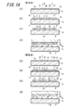
- the steps a1, b1, c1, and d1 of FIG. 1A correspond to the first manufacturing step of the semiconductor device using the substrate in the initial state that is not used for manufacturing the semiconductor device. Further, steps a2, b2, c2, and d2 in FIG. 1A show a substrate reuse step, and a substrate used at least once for manufacturing a semiconductor element was used. In addition, steps a3, b3, c3, and d3 of FIG. 1B show a further substrate reuse step. The steps a2 to d3 correspond to the second and subsequent manufacturing steps of the semiconductor element.
- step a1 shows a first mask forming step
- step a2 shows a second mask forming step
- Step b1 indicates a first element forming step
- step b2 indicates a second element forming step
- step c1 indicates a first mask removing step
- step c2 indicates a second mask removing step
- Step d1 indicates a first element separation step
- step d2 indicates a second element separation step.
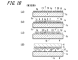
- the substrate 1 commonly used in each process is prepared before the process a1.
- the substrate 1 has one main surface (hereinafter, also referred to as the first surface) 1a, which is the starting point of semiconductor crystal growth, and the other main surface (hereinafter, also referred to as the second surface) located on the opposite side of the first surface 1a. ) 1b and.
- the surface layer of the substrate 1 including the first surface 1a is made of a nitride semiconductor.
- the substrate 1 used in the embodiment is, for example, a GaN substrate cut out from a gallium nitride (GaN) single crystal ingot.
- GaN gallium nitride
- the substrate 1 may be an n-type substrate in which impurities such as Si are doped in the nitride semiconductor, or may be a p-type substrate in which impurities such as Mg are doped in the nitride semiconductor.
- the impurity density in the substrate 1 is, for example, about 1 ⁇ 10 19 cm -3 or less.
- a Si substrate, a sapphire substrate, a SiC substrate, or the like may be used as the GaN substrate.
- the substrate 1 may be formed of the same type of material as the semiconductor layer 3 to be grown on the substrate 1, or may be formed of a different material.
- the GaN layer may be grown on the GaN substrate.
- the GaN layer may be grown on the Si substrate, the sapphire substrate, or the SiC substrate.
- the substrate 1 is not limited to a substrate whose surface layer is a GaN layer, and may be a substrate whose surface layer is composed of a GaN-based semiconductor.
- the second surface 1b of the substrate 1 located on the opposite side of the first surface 1a is formed by the alteration of the substrate 1 or the nitride semiconductor by the step described later.
- a protective layer 4 for suppressing decomposition may be formed.
- the protective layer 4 may contain, for example, aluminum oxide, alumina, or the like.
- the protective layer 4 may also be formed on the end surface 1c of the substrate 1 that connects the first surface 1a and the second surface 1b.
- the protective layer 4 is positioned on the second surface 1b of the substrate 1. As a result, deterioration of the second surface 1b of the substrate 1 can be reduced. As a result, the growth conditions of the semiconductor crystal can be stabilized and the mass productivity can be improved.
- the method for manufacturing a semiconductor element using the substrate 1 in the initial state mainly corresponds to the steps a1, b1, c1, d1 in FIG. 1A, and forms the first mask 21 on the first surface 1a of the substrate 1.
- the first mask forming step a1, the first element forming step b1 for forming the semiconductor layer 3 on the first surface 1a of the masked substrate 1, and the deposition suppression mask 2 (referred to as the first mask 21) are removed by etching.
- the first mask removing step c1 and the first element separating step d1 for separating the semiconductor layer 3 from the first surface 1a of the substrate 1 are included.
- a semiconductor crystal (semiconductor layer 3) is grown on the first surface 1a of the substrate 1 (GaN substrate) by using photolithography technology and etching technology.
- the deposition suppression mask 2 (first mask 21) to be suppressed is formed in a predetermined pattern.
- the first mask 21 is formed so that the first region R1 which is a part of the first surface 1a of the substrate 1 is exposed.
- the semiconductor layer 3 can be formed in the first region R1 in a later step.
- the first mask 21 is first formed on the entire surface of the first surface 1a.
- the first mask 21 may be, for example, a silicon oxide (SiO 2 ) layer.
- silicon oxide is laminated on the first surface 1a by about 30 to 500 nm by using a PCVD (Plasma Chemical Vapor Deposition) method or the like.
- a photoresist is applied to the surface of the first mask 21 formed on the entire surface of the first surface 1a, which is opposite to the surface facing the first surface 1a (the surface on the front side of the first mask 21), and the resist is applied. Form a layer (not shown).
- the photoresist may be a positive photoresist or a negative photoresist.
- the photomask may be, for example, a glass substrate on which a mask pattern is drawn with chromium (Cr), titanium (Ti), tungsten (W), or the like.
- the exposed and developed resist layer is cured, unnecessary parts of the first mask 21 that are not covered by the resist layer are subjected to HF (hydrofluoric acid) -based wet etching or a fluorine-based gas such as CF 4. Removed by dry etching with. Subsequently, by removing the resist layer, the first mask 21 having a predetermined pattern can be formed on the first surface 1a of the substrate 1.
- the resist layer can be removed by using a known method such as lift-off with a solvent and ashing.
- the exposed surface E1 seen from the region (upward opening) from which the first mask 21 has been removed by etching is the first region R1 where the first surface 1a is exposed, and the first region R1 is the first element forming step b1. This is the region that is the starting point for the growth of semiconductor crystals.
- the first region R1 is formed in a plurality of strips, for example.
- the opening width or groove width which is the width (width of one of the plurality of bands) in the parallel direction (horizontal direction in FIG. 1A) of the exposed surface E1, may be, for example, 2 to 20 ⁇ m. Further, the width of the first mask 21 in the parallel direction in the embodiment is set to, for example, 150 to 200 ⁇ m.
- the relationship between the width of the first mask 21 in the parallel direction and the width of the exposed surface E1 in the parallel direction is the first surface 1a of the substrate 1 of the semiconductor layer 3 formed in the subsequent first element forming step b1.
- the ratio of the crystal growth rate in the direction perpendicular to the above to the crystal growth rate in the direction parallel to the first surface 1a of the substrate 1 and the thickness of the semiconductor layer 3 to be grown may be taken into consideration.
- the pattern of the first mask 21 may be a band shape or a stripe shape, or a grid shape in which a plurality of band shapes are arranged so as to be orthogonal to each other in the vertical and horizontal directions. Any pattern may be used as long as it is a so-called repeat pattern in which openings divided at regular intervals (repeat pitch) are repeated a plurality of times.
- edge region 1e on the first surface 1a near the end surface 1c may also be covered with the first mask 21. This facilitates the separation of the semiconductor layer 3 in the subsequent first element separation step d1, and the semiconductor layer 3 located at the edge of the substrate 1 near the edge can also be separated neatly.
- the mask material constituting the first mask 21 for example, a material containing silicon oxide such as SiO 2 is used.
- the deposition suppression mask 2 may be any material as long as the semiconductor layer does not grow from the surface of the mask material due to vapor phase growth. Outside those containing silicon oxide, for example, zirconium oxide (ZrO X), titanium oxide (TiO X), it is possible to use an oxide such as aluminum oxide (AlO X).
- a transition metal selected from chromium (Cr), tungsten (W), molybdenum (Mo), tantalum (Ta), niobium (Nb) and the like may be used.
- a method for depositing the mask material a method suitable for the mask material such as thin film deposition, sputtering, and coating curing can be appropriately used.
- the semiconductor crystal is epitaxially grown (Epitaxial Lateral Overgrowth; ELO) so as to spread from the exposed surface E1 which is the first region R1 to the adjacent first mask 21.
- the semiconductor layer 3 (also referred to as the first semiconductor layer 31) forming a part of the element is formed.
- the semiconductor layer 3 in the embodiment is a nitride semiconductor, and by epitaxial growth, the nitride semiconductor is spread from the first surface 1a to the upper surface of the first mask 21 beyond the upper edge opening of the groove of the first mask 21. Grow.
- a vapor phase growth method such as the Metalorganic Chemical Vapor Deposition (MOCVD) method or the Molecular Beam Epitaxy (MBE) method can be used.
- the substrate 1 on which the first mask 21 is patterned is inserted into the reaction chamber of the epitaxial apparatus, and hydrogen gas, nitrogen gas, or hydrogen is used. While supplying a mixed gas of hydrogen and nitrogen and a group V raw material (containing a group 15 element) gas such as ammonia, the substrate 1 is heated to a predetermined growth temperature, for example, 1050 to 1100 ° C.
- a group III (group 13 element-containing) raw material such as trimethylgallium (TMG) is supplied to grow crystals.
- TMG trimethylgallium
- the semiconductor layer 3 is epitaxially grown from the exposed surface E1 which is a region (first region R1).
- a desired conductive type GaN layer can be obtained by supplying a raw material gas such as an n-type impurity such as Si or a p-type impurity such as Mg and adjusting the doping amount. Further, the supply of the raw material may be temporarily stopped to stop the growth of the semiconductor crystal before the growth crystal crosses the edge of the opening of the groove between the first masks 21 or the growth crystal fills the groove. In this way, the "fragile portion" that facilitates the separation of the semiconductor layer 3 in the first element separation step d1 may be formed as a partial layer or film before restarting the supply of the raw material.
- the fragile portion for example, when the GaN layer is crystal-grown, the upper portion of the semiconductor layer 3 located on the opening side in the groove of the first region R1 and the lower portion of the semiconductor layer 3 located on the exposed surface E1 side. In between, a layer made of a mixed crystal of GaN and BN, AlN, InN, etc. may be formed as a fragile portion.
- the semiconductor layer 3 may be formed.
- a fragile portion having a superlattice structure may be formed by alternately stacking AlGaN layers and GaN layers.
- the fragile portion may be formed by alternately laminating large layers of GaN crystal grains and small layers of crystal grains by periodically changing the crystal growth conditions.
- the fragile portion may be a layer in which the impurity concentration is changed by changing the concentration of silicon (Si) used as an n-type impurity of GaN.
- GaN When a fragile portion is formed, GaN is continuously vapor-deposited starting from the upper surface (surface) of the fragile portion. When the fragile portion is not formed, GaN is vapor-deposited starting from the exposed surface E1 between the first regions R1.
- the semiconductor layer 3 grows in the lateral direction (horizontal direction in FIG. 1A) along the upper surface of the deposition suppression mask 2. Therefore, through dislocations of the semiconductor layer 3 can be reduced.
- the first element forming step b1 is completed before each semiconductor layer 3 that has started to grow from the exposed surface E1 of the first region R1 comes into contact with or overlaps with the adjacent first semiconductor layer 31. As a result, it is possible to reduce crystal defects such as cracks or through dislocations that may occur when adjacent semiconductor layers 3 are in contact with each other.
- the semiconductor element in the first element forming step b1, at least a part of the semiconductor element may be formed, and not all the configurations of the semiconductor element may be formed before c1 before the first mask removing step. Further, when all the configurations of the semiconductor element are not formed, the remaining configurations of the semiconductor element may be formed after the first mask removing step c1 or after the first element separation step d1. Further, the configuration of the semiconductor element may be appropriately formed according to the type of the semiconductor element.
- the first semiconductor layer 31 has a substantially T-shaped shape connected to the substrate 1 by a thin connecting portion located on the exposed surface E1. As a result, the first semiconductor layer 31 can be smoothly separated.
- a member or jig such as a support substrate 6 having an adhesive layer 5 made of solder using a material such as AuSn is formed on one surface (lower surface).
- This is a step of separating at least a part (for example, the first semiconductor layer 31) of the semiconductor element formed in the first element forming step b1 from the substrate 1 and forming each into an individual semiconductor element S.
- the support substrate 6 having the adhesive layer 5 on the lower surface is opposed to the surface (first surface 1a) on which the first semiconductor layer 31 of the substrate 1 is formed. Subsequently, the support substrate 6 is pressed toward the substrate 1 and the adhesive layer 5 is heated to bond the semiconductor 3 to the adhesive layer 5.
- the first element separation step d1 may include a step of dividing the first semiconductor layer 31 according to the size of the semiconductor element S, and a step of forming an electrode, a wiring conductor, or the like on the first semiconductor layer 31.
- the first semiconductor layer 31 may be divided by cleavage on the cleavage plane.
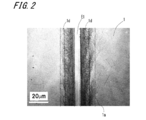
- FIG. 2 schematically shows a region (hereinafter, also referred to as a defect region) 1d in which a pit and a transition defect have occurred.
- FIG. 2 shows a state in which a transition defect is generated on the first surface 1a of the substrate 1.
- the method for manufacturing a semiconductor element according to the present invention includes a substrate reuse step of growing a semiconductor crystal (second semiconductor layer 32) again from a second region R2 that at least partially overlaps with the first region R1. There is.
- the second region R2 and the first region R1 are substantially coincident regions.
- the substrate reuse step includes a second substrate reuse step having “step a2” to “step d2”.
- “Step a2” indicates the second mask forming step a2
- “step b2” indicates the second element forming step b2
- “step c2” indicates the second mask removing step c2
- “step d2” indicates the second element.
- the separation step d2 is shown.
- the second substrate reuse step is carried out in a state where the first surface 1a exposed after the first element separation step d1 described above is not polished.
- at least a part of the first surface 1a is subjected to deposits adhering to the first surface 1a. It may be performed after the cleaning step of cleaning.
- (A2) Second Mask Forming Step In the second mask forming step a2, a photolithography technique and an etching technique are used to create a new area including the forming position of the first mask 21 formed in the first mask forming step a1.
- the deposition suppression mask 2 (also referred to as the second mask 22) is formed to expose the exposed surface (also referred to as the second crystal growth region (second region R2)) E2 not covered by the second mask 22.
- the second mask forming step a2 is composed of the first step to the fourth step.
- “step a21" indicates the first step
- step a22" indicates the second step
- step a23" indicates the third step
- step a24 indicates the fourth step.
- a deposition suppression mask 2 (second mask 22) is formed on the entire surface of the first surface 1a of the substrate 1.
- the second mask 22 may be, for example, a silicon oxide (SiO 2 ) layer having a thickness of about 30 to 500 nm.
- silicon oxide is laminated on the first surface 1a by about 30 to 500 nm by using a PCVD method or the like.
- (A22) Second Step In the second step a22, first, on the surface of the second mask 22 formed in the first step a21 opposite to the surface facing the substrate 1 (the surface on the front side of the second mask 22). A photoresist is applied to form the resist layer 7.
- the photoresist may be a positive photoresist or a negative photoresist.
- a photomask (not shown) on which a mask pattern corresponding to the mask pattern of the photomask used in the first mask forming step a1 is drawn is prepared.
- the photomask is, for example, a glass substrate on which a mask pattern is drawn with chromium (Cr), titanium (Ti), tungsten (W), or the like.
- the prepared photomask is positioned on the substrate 1 at a predetermined position in the same manner as in the first mask forming step a1, and then the pattern drawn on the photomask is exposed and developed on the resist layer.
- the photomask may be positioned with respect to the substrate 1 based on the outer shape of the substrate 1 and the photomask, the mask pattern drawn on the photomask, the position of the defect region 1d, and the like. Alignment marks for alignment are formed on the substrate 1 and the photomask, and in the first mask forming step a1 and the second mask forming step a2, the photomask is positioned with respect to the substrate 1 based on the alignment marks. May be good.
- the resist layer 7 is removed by using a known method such as lift-off with a solvent and ashing to expose the exposed surface E2 which at least partially overlaps the exposed surface E1.
- the second region R2 which at least partially overlaps the first region R1, can be exposed on the first surface 1a of the substrate 1.
- the second region R2 may be included in the first region R1 and does not have to completely coincide with the first region R1. Further, the second region R2 may include the defect region 1d as long as the normal semiconductor crystal can grow. The second region R2 may be smaller than the first region R1.
- the second mask 22 may be formed also in the edge region 1e of the first surface 1a.
- the semiconductor layer 3 can be easily separated in the second element separation step d2, and the semiconductor layer 3 existing in the vicinity of the edge portion located at the end of the substrate 1 can also be separated neatly.
- a semiconductor crystal is grown from the exposed surface E2, which is the second region R2, so as to spread over the upper surface of the adjacent second mask 22, and a part of the element is grown.
- the constituent semiconductor layer 3 (also referred to as the second semiconductor layer 32) is formed.
- the second element forming step b2 may be the same as the first element forming step b1.
- (C2) Second Mask Removal Step After the completion of the second element forming step b2, the second mask 22 is removed using an etchant that does not substantially invade the grown second semiconductor layer 32.
- the second mask removing step c2 may be the same as the first mask removing step c1.
- the second element separation step d2 is a step of separating the second semiconductor layer 32 from the substrate 1 and forming each into individual semiconductor elements S.
- the second element separation step d2 may be the same as the first element separation step d1.
- the first surface 1a of the substrate 1 is regenerated without removing pits and transition defects by polishing or the like. It can be used to form a second semiconductor device. This makes it possible to reduce the number of steps in the manufacture of semiconductor devices and improve productivity.
- the second substrate reuse step may be repeated twice or more.
- the method for manufacturing a semiconductor element of the embodiment it is possible to reduce a large decrease in the thickness of the substrate 1 due to polishing or the like.
- the substrate reuse step may further include a third substrate reuse step having "steps a3" to "step d3".
- “Step a3” indicates the third mask forming step a3
- “step b3” indicates the third element forming step b3
- “step c3” indicates the third mask removing step c3
- “step d3” indicates the third element.
- the separation step d3 is shown.
- (A3) Third Mask Forming Step In the third mask forming step a3, a new area including the forming position of the second mask 22 formed in the second mask forming step a2 is created by using the photolithography technique and the etching technique.
- the deposition suppression mask 2 (third mask 23) is formed to expose the exposed surface (also referred to as the third crystal growth region (third region R3)) E3 not covered by the third mask 23.
- the third mask forming step a3 is composed of the first step to the fourth step.
- “step a31” indicates the first step
- step a32” indicates the second step
- step a33” indicates the third step
- step a34” indicates the fourth step.
- the third mask forming step a3 may be performed after polishing the first surface 1a exposed after the second element separation step d2 described above, or may be performed without polishing. May be done. Even if polishing is performed before the third mask forming step a3, since the second mask removing step is interposed, the substrate 1 is consumed less than the case where the substrate 1 is polished for each element separation step. Can be reduced. Further, the third mask forming step a3 may be performed after the plurality of second substrate reuse steps. The second substrate reuse step and the third substrate reuse step may be performed a plurality of times, respectively, and the number of times of the second substrate reuse step may be larger than the number of times of the third substrate reuse step. ..
- a deposition suppression mask 2 (also referred to as a third mask 23) is formed on the entire surface of the first surface 1a of the substrate 1.
- the third mask 23 may be, for example, a silicon oxide (SiO 2 ) layer having a thickness of about 30 to 500 nm.
- silicon oxide is laminated on the first surface 1a by about 30 to 500 nm by using a PCVD method or the like.
- (A32) Second Step In the second step a32, first, on the surface of the third mask 23 formed in the first step a31 opposite to the surface facing the substrate 1 (the surface on the front side of the third mask 23). A photoresist is applied to form a resist layer 7.
- the photoresist may be a positive photoresist or a negative photoresist.
- a photomask (not shown) on which a mask pattern corresponding to the mask pattern of the photomask used in the second mask forming step a2 is drawn is prepared.
- the photomask is, for example, a glass substrate on which a mask pattern is drawn with chromium (Cr), titanium (Ti), tungsten (W), or the like.
- the prepared photomask is positioned on the substrate 1 at a predetermined position in the same manner as in the second mask forming step a2, and then the pattern drawn on the photomask is exposed and developed on the resist layer.
- the photomask may be positioned with respect to the substrate 1 based on the outer shape of the substrate 1 and the photomask, the mask pattern drawn on the photomask, the position of the defect region 1d, and the like. Alignment marks for alignment are formed on the substrate 1 and the photomask, and in the second mask forming step a2 and the third mask forming step a3, the photomask is positioned with respect to the substrate 1 based on the alignment marks. May be good.
- the resist layer 7 is removed by using a known method such as lift-off with a solvent and ashing to expose the exposed surface E3 which at least partially overlaps the exposed surface E2.
- the third region R3, which at least partially overlaps the second region R2, can be exposed on the first surface 1a of the substrate 1.
- the third region R3 need only be included in the second region R2, and does not have to completely coincide with the second region R2.
- the third region R3 may include the defect region 1d as long as the normal semiconductor crystal can grow. At least a part of the third region R3 may overlap with the first region R1. Further, the third region R3 may be separated from the first region R1. Further, the third region R3 may be smaller than the first region R1.
- the third mask 23 may be formed also in the edge region 1e of the first surface 1a.
- the semiconductor layer 3 can be easily separated in the third element separation step d3, and the semiconductor layer 3 existing in the vicinity of the edge portion located at the end of the substrate 1 can also be separated neatly.
- (B3) Third Element Forming Step In the third element forming step b3, a semiconductor crystal is grown from the exposed surface E3, which is the third region R3, so as to spread over the upper surface of the adjacent third mask 23, and a part of the element is formed.
- the constituent semiconductor layer 3 also referred to as the third semiconductor layer 33
- the third element forming step b3 may be the same as the second element forming step b2.
- (C3) Third Mask Removal Step After the completion of the third element forming step b3, the third mask 23 is removed using an etchant that does not substantially invade the grown third semiconductor layer 33.
- the third mask removing step c3 may be the same as the second mask removing step c2.
- the third element separation step d3 is a step of separating the third semiconductor layer 33 from the substrate 1 and forming each into individual semiconductor elements S.
- the third element separation step d3 may be the same as the second element separation step d2.
- the first surface 1a of the substrate 1 is reused without removing pits and transition defects by polishing or the like. can do. This makes it possible to reduce the number of steps in the manufacture of semiconductor devices and improve productivity.
- the productivity of the semiconductor element can be improved.
- the thickness of the substrate 1 after the second element or the third element is peeled off after the second substrate reuse step (second element separation step d2) or the third substrate reuse step (third element separation step d3). It may be further provided with a substrate growth step for increasing the size.
- the substrate 1 itself can be regenerated, and the semiconductor element can be manufactured again.
- the substrate 1 itself may be regenerated in the same manner as, for example, a single crystal ingot. Specifically, for example, it may be carried out by vapor phase growth or liquid phase growth.
- the second substrate reuse step is carried out after the first element separation step d1 without polishing the first surface 1a, but after the first element separation step d1, the second element is described.
- the first surface 1a may be polished before the forming step b2.
- the separation of the first element may be performed together with a part of the surface layer of the substrate 1 with which the first element is in contact.
- a part of the surface layer of the substrate 1 can be removed, and the surface of the substrate 1 having few defects can be newly exposed.
- steps such as polishing the entire first surface a can be skipped, and the productivity of the semiconductor element can be improved.
- the substrate 1 may be peeled off so as to apply stress.
- the first element may be separated after removing the region including the portion of the first semiconductor layer 31 in contact with the substrate 1. That is, the first semiconductor layer 31 located on the first mask is used as the first element (or a part of the first element), and after removing the other parts, the first element (or a part of the first element). May be separated using the adhesive layer 5 and the support substrate 6. At this time, the first mask may be removed after the adhesive layer 5 and the support substrate 6 are adhered to the first semiconductor layer 31. If the first mask is removed, the first element can be easily separated from the substrate 1.
- a material to which the material of the semiconductor layer 3 does not easily adhere can be used.
- a fluororesin layer can be used. It may be.
- the deposition suppression mask 2 may be treated with fluorine on the surface of a layer made of an inorganic or organic material.
- the deposition suppression mask 2 directly performs fluorine treatment on the first main surface a of the substrate 1 except for the first region R1, the second region R2 or the third region R3 to suppress the deposition. It may function as a mask 2. By using a fluorine-based material, the growth of the semiconductor layer 3 can be reduced.
- the first mask 21 is removed before separating the first element has been described, but the first mask 21 is not removed and is reused as the second mask 22 or the third mask 23. May be good.
- the semiconductor device manufacturing method of the present disclosure includes a process of preparing a substrate and A first element forming step of forming a first semiconductor layer in a first region on the surface of the substrate, and A first element separation step of separating the first semiconductor layer from the substrate, and A second element forming step of forming the second semiconductor layer in the second region of the surface of the substrate from which the first semiconductor layer is separated, and With At least a part of the second region is configured to overlap the first region.
- the productivity of the semiconductor device can be improved by reducing the number of steps in manufacturing the semiconductor device and improving the quality of the semiconductor device.
Abstract
A method for manufacturing a semiconductor element according to the present disclosure comprises a step of preparing a substrate, a first element forming step of forming a first semiconductor layer in a first region on the surface of the substrate, a first element separating step of separating the first semiconductor layer from the substrate, and a second element forming step of forming a second semiconductor layer in a second region on the surface of the substrate from which the first semiconductor layer has been separated. In this method for manufacturing a semiconductor element, at least a portion of the second region overlaps the first region.
Description
本開示は、半導体素子の製造方法に関する。
This disclosure relates to a method for manufacturing a semiconductor device.
従来技術の一例は、特許文献1および特許文献2に記載されている。
An example of the prior art is described in Patent Document 1 and Patent Document 2.
本開示の半導体素子の製造方法は、基板を準備する工程と、前記基板の表面の第1領域に第1半導体層を形成する第1素子形成工程と、前記第1半導体層を前記基板から分離する第1素子分離工程と、前記第1半導体層が分離した基板の表面の第2領域に第2半導体層を形成する第2素子形成工程と、を備えている。また本開示の半導体素子の製造方法では、前記第2領域の少なくとも一部は、前記第1領域に重ねる、構成である。
The semiconductor element manufacturing method of the present disclosure includes a step of preparing a substrate, a first element forming step of forming a first semiconductor layer in a first region on the surface of the substrate, and a step of separating the first semiconductor layer from the substrate. The first element separating step is provided, and the second element forming step of forming the second semiconductor layer in the second region on the surface of the substrate from which the first semiconductor layer is separated is provided. Further, in the method for manufacturing a semiconductor element of the present disclosure, at least a part of the second region is overlapped with the first region.
従来、半導体素子の製造方法として、基板上に開口部を有するマスクを形成した後、横方向エピタキシャル成長法を用いて、開口部に露出する露出面から半導体素子となる半導体層を成長させる方法が知られている(例えば、特許文献1,2を参照)。成長させた半導体層は、支持基板等に転写されて、基板から分離される。
Conventionally, as a method for manufacturing a semiconductor element, a method is known in which a mask having an opening is formed on a substrate and then a semiconductor layer to be a semiconductor element is grown from an exposed surface exposed to the opening by using a transverse epitaxial growth method. (See, for example, Patent Documents 1 and 2). The grown semiconductor layer is transferred to a support substrate or the like and separated from the substrate.
また、特許文献2は、GaN系半導体層を剥離する剥離工程と、前記剥離工程の後、剥離した後のGaN基板を用いて、マスク形成工程及び成長工程を行なうことが記載されている。
Further, Patent Document 2 describes that a peeling step of peeling a GaN-based semiconductor layer, and after the peeling step, a mask forming step and a growing step are performed using the peeled GaN substrate.
このような、半導体素子の製造方法では、生産性を向上させることが求められている。
In such a method for manufacturing a semiconductor element, it is required to improve productivity.
以下、本開示の実施形態について、図面を参照しつつ説明する。なお、本発明は、半導体素子の製造方法に関する。本発明に係る製造方法によって、製造される半導体素子は、例えば、発光素子、受光素子またはショットキーバリアダイオードであればよい。なお、発光素子の場合は、例えば、発光ダイオード(Light Emitting Diode;LED)およびレーザダイオード(Laser Diode;LD)素子であればよい。
Hereinafter, embodiments of the present disclosure will be described with reference to the drawings. The present invention relates to a method for manufacturing a semiconductor device. The semiconductor element manufactured by the manufacturing method according to the present invention may be, for example, a light emitting element, a light receiving element, or a Schottky barrier diode. In the case of a light emitting element, for example, a light emitting diode (Light Emitting Diode; LED) and a laser diode (Laser Diode; LD) element may be used.
図1Aの工程a1,b1,c1,d1は、半導体素子の製造に使用されていない初期状態の基板を用いた、半導体素子の第1回目の製造工程に相当する。また、図1Aの工程a2,b2,c2,d2は、基板再使用工程を示すものであり、半導体素子の製造に少なくとも1回使用された基板を用いた。また、図1Bの工程a3,b3,c3,d3は、さらなる基板再使用工程を示すものである。工程a2~d3は、半導体素子の第2回目以降の製造工程に相当する。
The steps a1, b1, c1, and d1 of FIG. 1A correspond to the first manufacturing step of the semiconductor device using the substrate in the initial state that is not used for manufacturing the semiconductor device. Further, steps a2, b2, c2, and d2 in FIG. 1A show a substrate reuse step, and a substrate used at least once for manufacturing a semiconductor element was used. In addition, steps a3, b3, c3, and d3 of FIG. 1B show a further substrate reuse step. The steps a2 to d3 correspond to the second and subsequent manufacturing steps of the semiconductor element.
図1Aにおいて、「工程a1」は第1マスク形成工程を示し、「工程a2」は第2マスク形成工程を示す。「工程b1」は第1素子形成工程を示し、「工程b2」は第2素子形成工程を示す。「工程c1」は第1マスク除去工程を示し、「工程c2」は第2マスク除去工程を示す。「工程d1」は第1素子分離工程を示し、「工程d2」は第2素子分離工程を示す。
In FIG. 1A, "step a1" shows a first mask forming step, and "step a2" shows a second mask forming step. “Step b1” indicates a first element forming step, and “step b2” indicates a second element forming step. “Step c1” indicates a first mask removing step, and “step c2” indicates a second mask removing step. “Step d1” indicates a first element separation step, and “step d2” indicates a second element separation step.
各工程で共通して使用する基板1は、工程a1の前に準備される。基板1は、半導体の結晶成長の起点となる一方主面(以下、第1面ともいう)1aと、第1面1aに対して反対側に位置する他方主面(以下、第2面ともいう)1bとを有する。基板1の、第1面1aを含む表面層は、窒化物半導体で構成されている。実施形態で使用する基板1は、例えば、窒化ガリウム(GaN)単結晶インゴットから切り出したGaN基板である。
The substrate 1 commonly used in each process is prepared before the process a1. The substrate 1 has one main surface (hereinafter, also referred to as the first surface) 1a, which is the starting point of semiconductor crystal growth, and the other main surface (hereinafter, also referred to as the second surface) located on the opposite side of the first surface 1a. ) 1b and. The surface layer of the substrate 1 including the first surface 1a is made of a nitride semiconductor. The substrate 1 used in the embodiment is, for example, a GaN substrate cut out from a gallium nitride (GaN) single crystal ingot.
基板1は、窒化物半導体中にSiなどの不純物がドープされたn型基板であってもよく、窒化物半導体中にMgなどの不純物がドープされたp型基板であってもよい。基板1における不純物密度は、例えば、1×1019cm-3程度以下である。また、基板1としては、GaN基板のほか、Si基板、サファイア基板、SiC基板等を使用してよい。基板1は、基板1上に成長させる半導体層3と同種の材料で形成されていてもよいし、異種の材料で形成されていてもよい。基板1が半導体層3と同種の材料で形成されている場合、例えばGaN基板上にGaN層を成長させてもよい。また基板1が半導体層3と異種の材料で形成されている場合、Si基板、サファイア基板またはSiC基板上にGaN層を成長させてもよい。
The substrate 1 may be an n-type substrate in which impurities such as Si are doped in the nitride semiconductor, or may be a p-type substrate in which impurities such as Mg are doped in the nitride semiconductor. The impurity density in the substrate 1 is, for example, about 1 × 10 19 cm -3 or less. Further, as the substrate 1, in addition to the GaN substrate, a Si substrate, a sapphire substrate, a SiC substrate, or the like may be used. The substrate 1 may be formed of the same type of material as the semiconductor layer 3 to be grown on the substrate 1, or may be formed of a different material. When the substrate 1 is made of the same material as the semiconductor layer 3, for example, the GaN layer may be grown on the GaN substrate. When the substrate 1 is made of a material different from that of the semiconductor layer 3, the GaN layer may be grown on the Si substrate, the sapphire substrate, or the SiC substrate.
基板1は、表面層がGaN層である基板に限定されることはなく、表面層がGaN系半導体で構成されている基板であってもよい。ここでいう「GaN系半導体」とは、例えば、AlxGayInzN(0≦x≦1;0≦y≦1;0≦z≦1;x+y+z=1)によって構成されるものいう。
The substrate 1 is not limited to a substrate whose surface layer is a GaN layer, and may be a substrate whose surface layer is composed of a GaN-based semiconductor. The "GaN-based semiconductor", for example, Al x Ga y In z N means intended to be constituted by a (0 ≦ x ≦ 1; x + y + z = 1 0 ≦ y ≦ 1;; 0 ≦ z ≦ 1).
半導体の結晶成長の起点となる第1面1aを除く、第1面1aに対して反対側に位置する基板1の第2面1bには、後述の工程による基板1の変質または窒化物半導体の分解を抑制するための保護層4が形成されてもよい。保護層4は、例えば、酸化アルミニウムまたはアルミナ等を含んでいてもよい。保護層4は、基板1の、第1面1aと第2面1bとを接続する端面1cにも形成されてもよい。
Except for the first surface 1a, which is the starting point of the crystal growth of the semiconductor, the second surface 1b of the substrate 1 located on the opposite side of the first surface 1a is formed by the alteration of the substrate 1 or the nitride semiconductor by the step described later. A protective layer 4 for suppressing decomposition may be formed. The protective layer 4 may contain, for example, aluminum oxide, alumina, or the like. The protective layer 4 may also be formed on the end surface 1c of the substrate 1 that connects the first surface 1a and the second surface 1b.
本実施形態では、基板1の第2面1bに保護層4を位置させている。その結果、基板1の第2面1bの変質を低減することができる。ひいては、半導体結晶の成長条件を安定させ、量産性を向上させることができる。
In the present embodiment, the protective layer 4 is positioned on the second surface 1b of the substrate 1. As a result, deterioration of the second surface 1b of the substrate 1 can be reduced. As a result, the growth conditions of the semiconductor crystal can be stabilized and the mass productivity can be improved.
初期状態の基板1を用いた半導体素子の製造方法は、主には、図1Aの工程a1,b1,c1,d1に相当し、基板1の第1面1a上に第1マスク21を形成する第1マスク形成工程a1と、マスクされた基板1の第1面1a上に半導体層3を形成する第1素子形成工程b1と、エッチングにより堆積抑制マスク2(第1マスク21という)を除去する第1マスク除去工程c1と、半導体層3を基板1の第1面1aから分離する第1素子分離工程d1と、を含む。
The method for manufacturing a semiconductor element using the substrate 1 in the initial state mainly corresponds to the steps a1, b1, c1, d1 in FIG. 1A, and forms the first mask 21 on the first surface 1a of the substrate 1. The first mask forming step a1, the first element forming step b1 for forming the semiconductor layer 3 on the first surface 1a of the masked substrate 1, and the deposition suppression mask 2 (referred to as the first mask 21) are removed by etching. The first mask removing step c1 and the first element separating step d1 for separating the semiconductor layer 3 from the first surface 1a of the substrate 1 are included.
(a1)第1マスク形成工程
第1マスク形成工程a1では、基板1(GaN基板)の第1面1a上に、フォトリソグラフィー技術およびエッチング技術を用いて、半導体結晶(半導体層3)の成長を抑制する堆積抑制マスク2(第1マスク21)を、所定のパターンに形成する。このとき、基板1の第1面1aの一部である第1領域R1が露出するように、第1マスク21を形成する。その結果、後の工程において、第1領域R1に半導体層3を形成することができる。 (A1) First Mask Forming Step In the first mask forming step a1, a semiconductor crystal (semiconductor layer 3) is grown on thefirst surface 1a of the substrate 1 (GaN substrate) by using photolithography technology and etching technology. The deposition suppression mask 2 (first mask 21) to be suppressed is formed in a predetermined pattern. At this time, the first mask 21 is formed so that the first region R1 which is a part of the first surface 1a of the substrate 1 is exposed. As a result, the semiconductor layer 3 can be formed in the first region R1 in a later step.
第1マスク形成工程a1では、基板1(GaN基板)の第1面1a上に、フォトリソグラフィー技術およびエッチング技術を用いて、半導体結晶(半導体層3)の成長を抑制する堆積抑制マスク2(第1マスク21)を、所定のパターンに形成する。このとき、基板1の第1面1aの一部である第1領域R1が露出するように、第1マスク21を形成する。その結果、後の工程において、第1領域R1に半導体層3を形成することができる。 (A1) First Mask Forming Step In the first mask forming step a1, a semiconductor crystal (semiconductor layer 3) is grown on the
具体的には、第1マスク形成工程a1では、先ず、第1面1aの全面に第1マスク21を形成する。第1マスク21は、例えば酸化ケイ素(SiO2)層としてよい。第1マスク形成工程a1では、PCVD(Plasma Chemical Vapor Deposition)法等を用いて、第1面1a上に酸化ケイ素を30~500nm程度積層する。
Specifically, in the first mask forming step a1, the first mask 21 is first formed on the entire surface of the first surface 1a. The first mask 21 may be, for example, a silicon oxide (SiO 2 ) layer. In the first mask forming step a1, silicon oxide is laminated on the first surface 1a by about 30 to 500 nm by using a PCVD (Plasma Chemical Vapor Deposition) method or the like.
次に、第1面1aの全面に形成した第1マスク21の、第1面1aに対向する面とは反対側の面(第1マスク21の表側の面)にフォトレジストを塗布し、レジスト層(図示せず)を形成する。フォトレジストは、ポジ型のフォトレジストでも、ネガ型のレジストでもよい。
Next, a photoresist is applied to the surface of the first mask 21 formed on the entire surface of the first surface 1a, which is opposite to the surface facing the first surface 1a (the surface on the front side of the first mask 21), and the resist is applied. Form a layer (not shown). The photoresist may be a positive photoresist or a negative photoresist.
次に、第1マスク21の所定のパターンに対応するマスクパターンが描かれたフォトマスク(図示せず)を準備する。続いて、フォトマスクを、基板1に対して、所定の位置に位置付けた後、フォトマスクに描かれたマスクパターンをレジスト層に露光および現像する。フォトマスクは、例えば、ガラス基板にクロム(Cr)、チタン(Ti)またはタングステン(W)等でマスクパターンが描かれたものでよい。
Next, prepare a photomask (not shown) on which a mask pattern corresponding to a predetermined pattern of the first mask 21 is drawn. Subsequently, after the photomask is positioned at a predetermined position with respect to the substrate 1, the mask pattern drawn on the photomask is exposed and developed on the resist layer. The photomask may be, for example, a glass substrate on which a mask pattern is drawn with chromium (Cr), titanium (Ti), tungsten (W), or the like.
次に、露光および現像したレジスト層を硬化させた後、レジスト層に覆われていない、第1マスク21の不要部位を、HF(フッ酸)系ウェットエッチング、またはCF4等のフッ素系のガスを用いたドライエッチングによって取り除く。続いて、レジスト層を取り除くことによって、基板1の第1面1a上に所定のパターンを有する第1マスク21を形成することができる。レジスト層は、溶剤によるリフトオフ、アッシング等公知の方法を用いて取り除くことができる。
Next, after the exposed and developed resist layer is cured, unnecessary parts of the first mask 21 that are not covered by the resist layer are subjected to HF (hydrofluoric acid) -based wet etching or a fluorine-based gas such as CF 4. Removed by dry etching with. Subsequently, by removing the resist layer, the first mask 21 having a predetermined pattern can be formed on the first surface 1a of the substrate 1. The resist layer can be removed by using a known method such as lift-off with a solvent and ashing.
エッチングによって第1マスク21が取り除かれた領域(上向き開口)から覗く露出面E1は、第1面1aが露出する第1領域R1であり、第1領域R1は、第1素子形成工程b1において、半導体結晶の成長の起点となる領域である。なお、第1領域R1は、例えば、複数の帯状に形成されていている。
The exposed surface E1 seen from the region (upward opening) from which the first mask 21 has been removed by etching is the first region R1 where the first surface 1a is exposed, and the first region R1 is the first element forming step b1. This is the region that is the starting point for the growth of semiconductor crystals. The first region R1 is formed in a plurality of strips, for example.
露出面E1の並行方向(図1Aにおける左右方向)における幅(複数の帯のうちの1つの帯の幅)である開口幅または溝幅は、例えば2~20μmでよい。また、実施形態における、第1マスク21の並行方向の幅は、例えば150~200μmに設定される。
The opening width or groove width, which is the width (width of one of the plurality of bands) in the parallel direction (horizontal direction in FIG. 1A) of the exposed surface E1, may be, for example, 2 to 20 μm. Further, the width of the first mask 21 in the parallel direction in the embodiment is set to, for example, 150 to 200 μm.
第1マスク21の並行方向の幅と、露出面E1の並行方向の幅との関係は、続いて行われる第1素子形成工程b1において形成される半導体層3の、基板1の第1面1aに垂直な方向の結晶成長速度と、基板1の第1面1aに平行な方向の結晶成長速度との比率、および、成長させる半導体層3の厚みを考慮して設定すればよい。
The relationship between the width of the first mask 21 in the parallel direction and the width of the exposed surface E1 in the parallel direction is the first surface 1a of the substrate 1 of the semiconductor layer 3 formed in the subsequent first element forming step b1. The ratio of the crystal growth rate in the direction perpendicular to the above to the crystal growth rate in the direction parallel to the first surface 1a of the substrate 1 and the thickness of the semiconductor layer 3 to be grown may be taken into consideration.
また、第1マスク21のパターンとしては、帯状またはストライプ状のほか、帯状体が縦横に直交するように複数配置した格子状であってもよい。一定の間隔(リピートピッチ)で分断された開口が複数回繰り返される、いわゆるリピート柄(パターン)であれば、どのようなパターンでもよい。
Further, the pattern of the first mask 21 may be a band shape or a stripe shape, or a grid shape in which a plurality of band shapes are arranged so as to be orthogonal to each other in the vertical and horizontal directions. Any pattern may be used as long as it is a so-called repeat pattern in which openings divided at regular intervals (repeat pitch) are repeated a plurality of times.
さらに、第1面1aにおける、端面1cに近傍した縁部領域1eも、第1マスク21で覆われていてもよい。これにより、後の第1素子分離工程d1における半導体層3の分離が容易になり、基板1の端に位置する、縁部近傍の半導体層3も、きれいに分離することができる。
Further, the edge region 1e on the first surface 1a near the end surface 1c may also be covered with the first mask 21. This facilitates the separation of the semiconductor layer 3 in the subsequent first element separation step d1, and the semiconductor layer 3 located at the edge of the substrate 1 near the edge can also be separated neatly.
また、第1マスク21(堆積抑制マスク2)を構成するマスク材料としては、例えばSiO2等の酸化シリコンを含むものを用いる。堆積抑制マスク2は、気相成長によって、マスク材料の表面を起点として、半導体層が成長しない材料であればよい。酸化シリコンを含むもの以外では、例えば、酸化ジルコニウム(ZrOX)、酸化チタン(TiOX)、酸化アルミニウム(AlOX)等の酸化物を用いることができる。ただし、堆積抑制マスク2は、クロム(Cr)、タングステン(W)、モリブデン(Mo)、タンタル(Ta)およびニオブ(Nb)等から選択される遷移金属を使用してもよい。また、マスク材料の堆積方法は、蒸着、スパッタ、および塗布硬化等、マスク材料に適合した方法を適宜用いることができる。
Further, as the mask material constituting the first mask 21 (deposition suppression mask 2), for example, a material containing silicon oxide such as SiO 2 is used. The deposition suppression mask 2 may be any material as long as the semiconductor layer does not grow from the surface of the mask material due to vapor phase growth. Outside those containing silicon oxide, for example, zirconium oxide (ZrO X), titanium oxide (TiO X), it is possible to use an oxide such as aluminum oxide (AlO X). However, as the deposition suppression mask 2, a transition metal selected from chromium (Cr), tungsten (W), molybdenum (Mo), tantalum (Ta), niobium (Nb) and the like may be used. Further, as a method for depositing the mask material, a method suitable for the mask material such as thin film deposition, sputtering, and coating curing can be appropriately used.
(b1)第1素子形成工程
第1素子形成工程b1では、第1領域R1である露出面E1から、隣接する第1マスク21上にかけて広がるように、半導体結晶をエピタキシャル成長(Epitaxial Lateral Overgrowth;ELO)させ、素子の一部を構成する半導体層3(第1半導体層31ともいう)を形成する。実施形態における半導体層3は窒化物半導体であり、エピタキシャル成長によって、窒化物半導体を、第1面1aから、第1マスク21の溝の上縁開口を越えて、第1マスク21の上面にまで、成長させる。 (B1) First Element Forming Step In the first element forming step b1, the semiconductor crystal is epitaxially grown (Epitaxial Lateral Overgrowth; ELO) so as to spread from the exposed surface E1 which is the first region R1 to the adjacent first mask 21. The semiconductor layer 3 (also referred to as the first semiconductor layer 31) forming a part of the element is formed. Thesemiconductor layer 3 in the embodiment is a nitride semiconductor, and by epitaxial growth, the nitride semiconductor is spread from the first surface 1a to the upper surface of the first mask 21 beyond the upper edge opening of the groove of the first mask 21. Grow.
第1素子形成工程b1では、第1領域R1である露出面E1から、隣接する第1マスク21上にかけて広がるように、半導体結晶をエピタキシャル成長(Epitaxial Lateral Overgrowth;ELO)させ、素子の一部を構成する半導体層3(第1半導体層31ともいう)を形成する。実施形態における半導体層3は窒化物半導体であり、エピタキシャル成長によって、窒化物半導体を、第1面1aから、第1マスク21の溝の上縁開口を越えて、第1マスク21の上面にまで、成長させる。 (B1) First Element Forming Step In the first element forming step b1, the semiconductor crystal is epitaxially grown (Epitaxial Lateral Overgrowth; ELO) so as to spread from the exposed surface E1 which is the first region R1 to the adjacent first mask 21. The semiconductor layer 3 (also referred to as the first semiconductor layer 31) forming a part of the element is formed. The
第1素子形成工程b1では、III族(第13族元素)原料に塩化物を用いるハイドライド気相成長(Hydride Vapor Phase Epitaxy;HVPE)法、III族原料に有機金属を用いる有機金属気相成長(Metal Organic Chemical Vapor Deposition;MOCVD)法、または分子線気相成長(Molecular Beam Epitaxy;MBE)法等の気相成長法を用いることができる。
In the first element forming step b1, a hydride vapor phase growth (Hydride Vapor Phase Epitaxy; HVPE) method using chloride as a Group III (Group 13 element) raw material, and an organic metal vapor phase growth using an organic metal as a Group III raw material (Hydride Vapor Phase Epitaxy; HVPE) A vapor phase growth method such as the Metalorganic Chemical Vapor Deposition (MOCVD) method or the Molecular Beam Epitaxy (MBE) method can be used.
例えば、半導体層3であるGaN層をMOCVD法で成長させる場合、先ず、第1マスク21がパターン形成された基板1を、エピタキシャル装置の反応室に挿入し、水素ガス、窒素ガス、または、水素と窒素の混合ガスと、アンモニア等のV族原料(第15族元素含有)ガスを供給しながら、基板1を加熱して、所定の成長温度、例えば1050~1100℃まで、昇温させる。
For example, when the GaN layer, which is the semiconductor layer 3, is grown by the MOCVD method, first, the substrate 1 on which the first mask 21 is patterned is inserted into the reaction chamber of the epitaxial apparatus, and hydrogen gas, nitrogen gas, or hydrogen is used. While supplying a mixed gas of hydrogen and nitrogen and a group V raw material (containing a group 15 element) gas such as ammonia, the substrate 1 is heated to a predetermined growth temperature, for example, 1050 to 1100 ° C.
続いて、基板1の温度が安定してから、上記の混合ガスおよびV族原料ガスの他に、トリメチルガリウム(TMG)等のIII族(第13族元素含有)原料を供給して、結晶成長領域(第1領域R1)である露出面E1から半導体層3をエピタキシャル成長させる。
Subsequently, after the temperature of the substrate 1 stabilizes, in addition to the above-mentioned mixed gas and group V raw material gas, a group III (group 13 element-containing) raw material such as trimethylgallium (TMG) is supplied to grow crystals. The semiconductor layer 3 is epitaxially grown from the exposed surface E1 which is a region (first region R1).
このとき、Si等のn型不純物またはMg等のp型不純物等の原料ガスを供給し、ドープ量を調整することにより、所望の導電型のGaN層を得ることができる。また、成長結晶が第1マスク21間の溝の開口の縁を越える、または成長結晶が溝を埋め尽くす前に、原料の供給を一旦止めて、半導体結晶の成長を停止させてもよい。このようにして、原料の供給を再開させる前に、第1素子分離工程d1における半導体層3の分離を容易にする「脆弱部」を、部分的な層または膜として形成してもよい。
At this time, a desired conductive type GaN layer can be obtained by supplying a raw material gas such as an n-type impurity such as Si or a p-type impurity such as Mg and adjusting the doping amount. Further, the supply of the raw material may be temporarily stopped to stop the growth of the semiconductor crystal before the growth crystal crosses the edge of the opening of the groove between the first masks 21 or the growth crystal fills the groove. In this way, the "fragile portion" that facilitates the separation of the semiconductor layer 3 in the first element separation step d1 may be formed as a partial layer or film before restarting the supply of the raw material.
脆弱部の例としては、例えば、GaN層を結晶成長させる場合、第1領域R1の溝内における開口側に位置した半導体層3の上部と露出面E1側に位置した半導体層3の下部との間に、GaNと、BN、AlN、InN等との混晶結晶からなる層を、脆弱部として形成してもよい。
As an example of the fragile portion, for example, when the GaN layer is crystal-grown, the upper portion of the semiconductor layer 3 located on the opening side in the groove of the first region R1 and the lower portion of the semiconductor layer 3 located on the exposed surface E1 side. In between, a layer made of a mixed crystal of GaN and BN, AlN, InN, etc. may be formed as a fragile portion.
上記の他、脆弱部として、結晶成長層とは格子定数の異なる、AlxGayInzN(0≦x≦1;0≦y<1;0≦z≦1;x+y+z=1)からなる半導体層3を形成してもよい。また、AlGaN層とGaN層を交互に積層した、超格子構造の脆弱部を形成してもよい。脆弱部は、結晶の成長条件を周期的に変化させて、GaNの結晶粒の大きい層と結晶粒の小さな層とを交互に積層したものであってもよい。脆弱部は、GaNのn型不純物として使用されるシリコン(Si)の濃度を変化させる等して、不純物濃度を変化させた層であってもよい。
Besides the above, as fragile part, different lattice constants, Al x Ga y In z N is the crystal growth layer made of (0 ≦ x ≦ 1; x + y + z = 1 0 ≦ y <1;; 0 ≦ z ≦ 1) The semiconductor layer 3 may be formed. Further, a fragile portion having a superlattice structure may be formed by alternately stacking AlGaN layers and GaN layers. The fragile portion may be formed by alternately laminating large layers of GaN crystal grains and small layers of crystal grains by periodically changing the crystal growth conditions. The fragile portion may be a layer in which the impurity concentration is changed by changing the concentration of silicon (Si) used as an n-type impurity of GaN.
脆弱部を形成することによって、半導体素子Sを基板1から分離するとき、脆弱部に応力が集中して亀裂を発生させ易くなり、半導体素子Sを基板1から容易に分離することができる。
By forming the fragile portion, when the semiconductor element S is separated from the substrate 1, stress is concentrated on the fragile portion and cracks are likely to occur, so that the semiconductor element S can be easily separated from the substrate 1.
脆弱部を形成した場合には、その脆弱部の上面(表面)を起点として、続けてGaNを気相成長させる。脆弱部を形成しない場合には、第1領域R1の間の露出面E1を起点として、GaNを気相成長させる。
When a fragile portion is formed, GaN is continuously vapor-deposited starting from the upper surface (surface) of the fragile portion. When the fragile portion is not formed, GaN is vapor-deposited starting from the exposed surface E1 between the first regions R1.
半導体層3は、結晶成長面が第1マスク21の上縁を越えた後は、堆積抑制マスク2の上面に沿って横方向(図1Aにおける左右方向)に成長する。そのため、半導体層3の貫通転位などを低減することができる。
After the crystal growth surface exceeds the upper edge of the first mask 21, the semiconductor layer 3 grows in the lateral direction (horizontal direction in FIG. 1A) along the upper surface of the deposition suppression mask 2. Therefore, through dislocations of the semiconductor layer 3 can be reduced.
第1素子形成工程b1は、第1領域R1の露出面E1から成長を始めた各半導体層3が、隣接する第1半導体層31に接触または互いに重なる前に終了する。その結果、隣接する半導体層3同士が接した際に発生し得るクラックまたは貫通転位等の結晶欠陥を低減することができる。
The first element forming step b1 is completed before each semiconductor layer 3 that has started to grow from the exposed surface E1 of the first region R1 comes into contact with or overlaps with the adjacent first semiconductor layer 31. As a result, it is possible to reduce crystal defects such as cracks or through dislocations that may occur when adjacent semiconductor layers 3 are in contact with each other.
なお、第1素子形成工程b1では、半導体素子の少なくとも一部を形成すればよく、第1マスク除去工程前c1に、半導体素子の全ての構成が形成されていなくてもよい。また、半導体素子の全ての構成が形成されていない場合、第1マスク除去工程c1の後、または第1素子分離工程d1の後に半導体素子の残りの構成を形成してもよい。また、半導体素子の構成は、半導体素子の種類に応じて、適宜形成すればよい。
Note that in the first element forming step b1, at least a part of the semiconductor element may be formed, and not all the configurations of the semiconductor element may be formed before c1 before the first mask removing step. Further, when all the configurations of the semiconductor element are not formed, the remaining configurations of the semiconductor element may be formed after the first mask removing step c1 or after the first element separation step d1. Further, the configuration of the semiconductor element may be appropriately formed according to the type of the semiconductor element.
(c1)第1マスク除去工程
第1素子形成工程b1の完了後、基板1を気相成長装置(エピタキシャル装置)から取り出し、成長した半導体層3を実質的に侵さないエッチャントを用いて、第1マスク21を除去する。 (C1) First Mask Removal Step After the completion of the first element forming step b1, thesubstrate 1 is taken out from the vapor phase growth apparatus (epitaxial apparatus), and the first is used using an etchant that does not substantially invade the grown semiconductor layer 3. Remove the mask 21.
第1素子形成工程b1の完了後、基板1を気相成長装置(エピタキシャル装置)から取り出し、成長した半導体層3を実質的に侵さないエッチャントを用いて、第1マスク21を除去する。 (C1) First Mask Removal Step After the completion of the first element forming step b1, the
第1マスク21の除去は、例えば、SiO2膜からなるマスクの場合、HF系ウェットエッチングを行なう。エッチングによって、第1マスク21が除去される。第1半導体層31は、図1Aの(c1)に示すように、露出面E1上に位置する細い接続部によって基板1と接続された、略T字状の形状となる。これにより、第1半導体層31の分離を円滑に行なうことができるようになる。
To remove the first mask 21, for example, in the case of a mask made of a SiO 2 film, HF-based wet etching is performed. The first mask 21 is removed by etching. As shown in FIG. 1A (c1), the first semiconductor layer 31 has a substantially T-shaped shape connected to the substrate 1 by a thin connecting portion located on the exposed surface E1. As a result, the first semiconductor layer 31 can be smoothly separated.
(d1)第1素子分離工程
第1素子分離工程d1は、1つの面(下面)に、AuSn等の材料を用いた半田からなる接着層5を有する支持基板6などの部材または治具などを用いて、第1素子形成工程b1で形成した半導体素子の少なくとも一部を(例えば、第1半導体層31)を基板1から分離し、それぞれ、個々の半導体素子Sとする工程である。 (D1) First Element Separation Step In the first element separation step d1, a member or jig such as asupport substrate 6 having an adhesive layer 5 made of solder using a material such as AuSn is formed on one surface (lower surface). This is a step of separating at least a part (for example, the first semiconductor layer 31) of the semiconductor element formed in the first element forming step b1 from the substrate 1 and forming each into an individual semiconductor element S.
第1素子分離工程d1は、1つの面(下面)に、AuSn等の材料を用いた半田からなる接着層5を有する支持基板6などの部材または治具などを用いて、第1素子形成工程b1で形成した半導体素子の少なくとも一部を(例えば、第1半導体層31)を基板1から分離し、それぞれ、個々の半導体素子Sとする工程である。 (D1) First Element Separation Step In the first element separation step d1, a member or jig such as a
例えば、下面に接着層5を有する支持基板6を、基板1の第1半導体層31が形成された面(第1面1a)に対向させる。続いて、支持基板6を基板1に向けて押圧し、接着層5を加熱することによって、半導体3を接着層5に接着させる。
For example, the support substrate 6 having the adhesive layer 5 on the lower surface is opposed to the surface (first surface 1a) on which the first semiconductor layer 31 of the substrate 1 is formed. Subsequently, the support substrate 6 is pressed toward the substrate 1 and the adhesive layer 5 is heated to bond the semiconductor 3 to the adhesive layer 5.
その後、接着層5に接着し一体となった第1半導体層31を、上方に引き剥がすように外力を加え、これら第1半導体層31を、基板1の第1面1aから引き上げる。これにより、半導体素子Sの本体を、傷付けることなく分離することができる。第1素子分離工程d1は、半導体素子Sのサイズに合わせて、第1半導体層31を分割する工程、および第1半導体層31に電極、配線導体等を形成する工程を含んでいてもよい。なお、第1半導体層31を分割する際には、第1半導体層31を劈開面で劈開することによって分割してもよい。
After that, an external force is applied so as to peel the first semiconductor layer 31 adhered to and integrated with the adhesive layer 5 upward, and these first semiconductor layers 31 are pulled up from the first surface 1a of the substrate 1. As a result, the main body of the semiconductor element S can be separated without being damaged. The first element separation step d1 may include a step of dividing the first semiconductor layer 31 according to the size of the semiconductor element S, and a step of forming an electrode, a wiring conductor, or the like on the first semiconductor layer 31. When the first semiconductor layer 31 is divided, the first semiconductor layer 31 may be divided by cleavage on the cleavage plane.
次に、第1素子分離工程d1の完了後に1回以上行われる、基板再使用工程について説明する。
Next, the substrate reuse step, which is performed once or more after the completion of the first element separation step d1, will be described.
第1半導体層31を分離した後の基板1では、第1面1aにおける第1マスク21に覆われていた領域に、第1面1aから基板1の内部に至るピット、および第1面1aに沿った転移欠陥が発生することがある。図2は、ピットおよび転移欠陥が発生した領域(以下、欠陥領域ともいう)1dを模式的に示している。図2は、基板1の第1面1aにおける転移欠陥の発生状態を示している。
In the substrate 1 after the first semiconductor layer 31 is separated, the area covered by the first mask 21 on the first surface 1a, the pit extending from the first surface 1a to the inside of the substrate 1, and the first surface 1a. Transfer defects along the line may occur. FIG. 2 schematically shows a region (hereinafter, also referred to as a defect region) 1d in which a pit and a transition defect have occurred. FIG. 2 shows a state in which a transition defect is generated on the first surface 1a of the substrate 1.
欠陥領域1dから高品質の半導体結晶を成長させることは困難である。このため、第1面1a上に堆積抑制マスク2を無作為に再形成し、第1面1aから半導体結晶を再度成長させるためには、研磨等の処理を第1面1aに施す必要がある。
It is difficult to grow a high quality semiconductor crystal from the defect region 1d. Therefore, in order to randomly reshape the deposition suppression mask 2 on the first surface 1a and re-grow the semiconductor crystal from the first surface 1a, it is necessary to perform a treatment such as polishing on the first surface 1a. ..
それに対して、第1面1aにおける第1領域R1、すなわち第1面1aにおける半導体層3(第1半導体層31)と接続していた領域には、ピットが少ない。また、例えば図2に示すように、第1領域R1には、転移欠陥が存在しないか、初期状態の基板1と同程度の面密度(例えば、1×10⁷/cm2以下)でしか転移欠陥が存在しない。したがって、本発明に係る半導体素子の製造方法では、第1領域R1と少なくとも一部が重なる第2領域R2から半導体結晶(第2半導体層32)を再度成長させる、基板再使用工程を有している。これにより、研磨等によってピットおよび転移欠陥を取り除くことを低減することができ、初期状態の基板1と同程度のピット密度および転移欠陥密度の領域から半導体結晶を成長させることができ、ひいては、半導体素子の生産性を向上させることができる。なお、本実施形態では、第2領域R2および第1領域R1は、略一致する領域である。
On the other hand, there are few pits in the first region R1 on the first surface 1a, that is, the region connected to the semiconductor layer 3 (first semiconductor layer 31) on the first surface 1a. Further, for example, as shown in FIG. 2, the first region R1 has no transfer defect or is transferred only at the same surface density as the substrate 1 in the initial state (for example, 1 × 10 7 / cm 2 or less). There are no defects. Therefore, the method for manufacturing a semiconductor element according to the present invention includes a substrate reuse step of growing a semiconductor crystal (second semiconductor layer 32) again from a second region R2 that at least partially overlaps with the first region R1. There is. As a result, it is possible to reduce the removal of pits and transition defects by polishing or the like, and it is possible to grow a semiconductor crystal from a region having a pit density and a transition defect density similar to that of the substrate 1 in the initial state, and by extension, a semiconductor. The productivity of the device can be improved. In the present embodiment, the second region R2 and the first region R1 are substantially coincident regions.
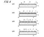
図1Aに示すように、基板再使用工程は、「工程a2」~「工程d2」を有する第2基板再使用工程を有している。「工程a2」は第2マスク形成工程a2を示し、「工程b2」は第2素子形成工程b2を示し、「工程c2」は第2マスク除去工程c2を示し、「工程d2」は第2素子分離工程d2を示す。なお、第2基板再使用工程は、上述した第1素子分離工程d1の後に露出した第1面1aに対して、研磨が行なわれていない状態で、実施される。なお、第2基板再使用工程で、第1素子分離工程d1の後、第2素子形成工程b2の前に第1面1aの少なくとも一部に対して、第1面1aに付着する付着物を洗浄する洗浄工程の後に行なわれてもよい。
As shown in FIG. 1A, the substrate reuse step includes a second substrate reuse step having “step a2” to “step d2”. “Step a2” indicates the second mask forming step a2, “step b2” indicates the second element forming step b2, “step c2” indicates the second mask removing step c2, and “step d2” indicates the second element. The separation step d2 is shown. The second substrate reuse step is carried out in a state where the first surface 1a exposed after the first element separation step d1 described above is not polished. In the second substrate reuse step, after the first element separation step d1 and before the second element forming step b2, at least a part of the first surface 1a is subjected to deposits adhering to the first surface 1a. It may be performed after the cleaning step of cleaning.
(a2)第2マスク形成工程
第2マスク形成工程a2では、フォトリソグラフィー技術およびエッチング技術を用いて、第1マスク形成工程a1で形成された第1マスク21の形成位置を含む領域に、新たな堆積抑制マスク2(第2マスク22ともいう)を形成して、第2マスク22に覆われていない露出面(第2の結晶成長領域(第2領域R2)ともいう)E2を露出させる。第2マスク形成工程a2は、第1工程~第4工程によって構成される。図3において、「工程a21」は第1工程を示し、「工程a22」は第2工程を示し、「工程a23」は第3工程を示し、「工程a24」は第4工程を示す。 (A2) Second Mask Forming Step In the second mask forming step a2, a photolithography technique and an etching technique are used to create a new area including the forming position of the first mask 21 formed in the first mask forming step a1. The deposition suppression mask 2 (also referred to as the second mask 22) is formed to expose the exposed surface (also referred to as the second crystal growth region (second region R2)) E2 not covered by the second mask 22. The second mask forming step a2 is composed of the first step to the fourth step. In FIG. 3, "step a21" indicates the first step, "step a22" indicates the second step, "step a23" indicates the third step, and "step a24" indicates the fourth step.
第2マスク形成工程a2では、フォトリソグラフィー技術およびエッチング技術を用いて、第1マスク形成工程a1で形成された第1マスク21の形成位置を含む領域に、新たな堆積抑制マスク2(第2マスク22ともいう)を形成して、第2マスク22に覆われていない露出面(第2の結晶成長領域(第2領域R2)ともいう)E2を露出させる。第2マスク形成工程a2は、第1工程~第4工程によって構成される。図3において、「工程a21」は第1工程を示し、「工程a22」は第2工程を示し、「工程a23」は第3工程を示し、「工程a24」は第4工程を示す。 (A2) Second Mask Forming Step In the second mask forming step a2, a photolithography technique and an etching technique are used to create a new area including the forming position of the first mask 21 formed in the first mask forming step a1. The deposition suppression mask 2 (also referred to as the second mask 22) is formed to expose the exposed surface (also referred to as the second crystal growth region (second region R2)) E2 not covered by the second mask 22. The second mask forming step a2 is composed of the first step to the fourth step. In FIG. 3, "step a21" indicates the first step, "step a22" indicates the second step, "step a23" indicates the third step, and "step a24" indicates the fourth step.
(a21)第1工程
第1工程a21では、基板1の第1面1aの全面に堆積抑制マスク2(第2マスク22)を形成する。第2マスク22は、例えば厚さ30~500nm程度の酸化ケイ素(SiO2)層でよい。第1工程a21では、例えば、PCVD法等を用いて、第1面1a上に酸化ケイ素を30~500nm程度積層する。 (A21) First Step In the first step a21, a deposition suppression mask 2 (second mask 22) is formed on the entire surface of thefirst surface 1a of the substrate 1. The second mask 22 may be, for example, a silicon oxide (SiO 2 ) layer having a thickness of about 30 to 500 nm. In the first step a21, for example, silicon oxide is laminated on the first surface 1a by about 30 to 500 nm by using a PCVD method or the like.
第1工程a21では、基板1の第1面1aの全面に堆積抑制マスク2(第2マスク22)を形成する。第2マスク22は、例えば厚さ30~500nm程度の酸化ケイ素(SiO2)層でよい。第1工程a21では、例えば、PCVD法等を用いて、第1面1a上に酸化ケイ素を30~500nm程度積層する。 (A21) First Step In the first step a21, a deposition suppression mask 2 (second mask 22) is formed on the entire surface of the
(a22)第2工程
第2工程a22では、先ず、第1工程a21で形成した第2マスク22の、基板1に対向する面とは反対側の面(第2マスク22の表側の面)にフォトレジストを塗布し、レジスト層7を形成する。フォトレジストは、ポジ型のフォトレジストでも、ネガ型のレジストでもよい。 (A22) Second Step In the second step a22, first, on the surface of the second mask 22 formed in the first step a21 opposite to the surface facing the substrate 1 (the surface on the front side of the second mask 22). A photoresist is applied to form the resistlayer 7. The photoresist may be a positive photoresist or a negative photoresist.
第2工程a22では、先ず、第1工程a21で形成した第2マスク22の、基板1に対向する面とは反対側の面(第2マスク22の表側の面)にフォトレジストを塗布し、レジスト層7を形成する。フォトレジストは、ポジ型のフォトレジストでも、ネガ型のレジストでもよい。 (A22) Second Step In the second step a22, first, on the surface of the second mask 22 formed in the first step a21 opposite to the surface facing the substrate 1 (the surface on the front side of the second mask 22). A photoresist is applied to form the resist
次に、第1マスク形成工程a1で使用したフォトマスクのマスクパターンに対応するマスクパターンが描かれたフォトマスク(図示せず)を準備する。フォトマスクは、例えば、ガラス基板にクロム(Cr)、チタン(Ti)またはタングステン(W)等でマスクパターンが描かれたものである。続いて、準備したフォトマスクを、基板1に対して、第1マスク形成工程a1と同様に、所定の位置に位置付けた後、フォトマスクに描かれたパターンをレジスト層に露光および現像する。
Next, a photomask (not shown) on which a mask pattern corresponding to the mask pattern of the photomask used in the first mask forming step a1 is drawn is prepared. The photomask is, for example, a glass substrate on which a mask pattern is drawn with chromium (Cr), titanium (Ti), tungsten (W), or the like. Subsequently, the prepared photomask is positioned on the substrate 1 at a predetermined position in the same manner as in the first mask forming step a1, and then the pattern drawn on the photomask is exposed and developed on the resist layer.
フォトマスクは、基板1およびフォトマスクの外形形状、フォトマスクに描かれたマスクパターン、欠陥領域1dの位置等に基づいて、基板1に対して位置付けられてもよい。基板1およびフォトマスクに位置合わせ用のアライメントマークを形成しておき、第1マスク形成工程a1および第2マスク形成工程a2では、フォトマスクを、アライメントマークに基づいて、基板1に対して位置付けてもよい。
The photomask may be positioned with respect to the substrate 1 based on the outer shape of the substrate 1 and the photomask, the mask pattern drawn on the photomask, the position of the defect region 1d, and the like. Alignment marks for alignment are formed on the substrate 1 and the photomask, and in the first mask forming step a1 and the second mask forming step a2, the photomask is positioned with respect to the substrate 1 based on the alignment marks. May be good.
(a23)第3工程
第3工程a23では、所定のパターンに露光および現像したレジスト層7を硬化させた後、レジスト層7に覆われていない、第2マスク22の不要部位を、HF(フッ酸)系ウェットエッチング、または、CF4等のフッ素系のガスを用いたドライエッチングによって取り除く。 (A23) Third Step In the third step a23, after curing the resistlayer 7 exposed and developed in a predetermined pattern, the unnecessary portion of the second mask 22 that is not covered by the resist layer 7 is HF (fluorinated). It is removed by acid) -based wet etching or dry etching using a fluorine-based gas such as CF 4.
第3工程a23では、所定のパターンに露光および現像したレジスト層7を硬化させた後、レジスト層7に覆われていない、第2マスク22の不要部位を、HF(フッ酸)系ウェットエッチング、または、CF4等のフッ素系のガスを用いたドライエッチングによって取り除く。 (A23) Third Step In the third step a23, after curing the resist
(a24)第4工程
第4工程a24では、溶剤によるリフトオフ、アッシング等公知の方法を用いて、レジスト層7を取り除き、露出面E1と少なくとも一部が重なる露出面E2を露出させる。 (A24) Fourth Step In the fourth step a24, the resistlayer 7 is removed by using a known method such as lift-off with a solvent and ashing to expose the exposed surface E2 which at least partially overlaps the exposed surface E1.
第4工程a24では、溶剤によるリフトオフ、アッシング等公知の方法を用いて、レジスト層7を取り除き、露出面E1と少なくとも一部が重なる露出面E2を露出させる。 (A24) Fourth Step In the fourth step a24, the resist
上記の第2マスク形成工程a2によって、基板1の第1面1aに、第1領域R1に少なくとも一部が重なる第2領域R2を露出させることができる。第2領域R2は、第1領域R1に含まれていればよく、第1領域R1に完全に一致している必要はない。また、第2領域R2は、正常な半導体結晶の成長が可能な範囲であれば、欠陥領域1dを含んでいてもよい。なお、第2領域R2は、第1領域R1よりも小さくてもよい。
By the second mask forming step a2 described above, the second region R2, which at least partially overlaps the first region R1, can be exposed on the first surface 1a of the substrate 1. The second region R2 may be included in the first region R1 and does not have to completely coincide with the first region R1. Further, the second region R2 may include the defect region 1d as long as the normal semiconductor crystal can grow. The second region R2 may be smaller than the first region R1.
第2マスク形成工程a2では、第1面1aの縁部領域1eにも第2マスク22を形成してもよい。これにより、第2素子分離工程d2における半導体層3の分離が容易になり、基板1の端に位置する縁部の近傍に存在する半導体層3も、きれいに分離することができる。
In the second mask forming step a2, the second mask 22 may be formed also in the edge region 1e of the first surface 1a. As a result, the semiconductor layer 3 can be easily separated in the second element separation step d2, and the semiconductor layer 3 existing in the vicinity of the edge portion located at the end of the substrate 1 can also be separated neatly.
(b2)第2素子形成工程
第2素子形成工程b2では、第2領域R2である露出面E2から、隣接する第2マスク22の上面に広がるように半導体結晶を成長させ、素子の一部を構成する半導体層3(第2半導体層32ともいう)を形成する。第2素子形成工程b2は、第1素子形成工程b1と同様であればよい。 (B2) Second Element Forming Step In the second element forming step b2, a semiconductor crystal is grown from the exposed surface E2, which is the second region R2, so as to spread over the upper surface of the adjacent second mask 22, and a part of the element is grown. The constituent semiconductor layer 3 (also referred to as the second semiconductor layer 32) is formed. The second element forming step b2 may be the same as the first element forming step b1.
第2素子形成工程b2では、第2領域R2である露出面E2から、隣接する第2マスク22の上面に広がるように半導体結晶を成長させ、素子の一部を構成する半導体層3(第2半導体層32ともいう)を形成する。第2素子形成工程b2は、第1素子形成工程b1と同様であればよい。 (B2) Second Element Forming Step In the second element forming step b2, a semiconductor crystal is grown from the exposed surface E2, which is the second region R2, so as to spread over the upper surface of the adjacent second mask 22, and a part of the element is grown. The constituent semiconductor layer 3 (also referred to as the second semiconductor layer 32) is formed. The second element forming step b2 may be the same as the first element forming step b1.
(c2)第2マスク除去工程
第2素子形成工程b2の完了後、成長した第2半導体層32を実質的に侵さないエッチャントを用いて、第2マスク22を除去する。第2マスク除去工程c2は、第1マスク除去工程c1と同様であればよい。 (C2) Second Mask Removal Step After the completion of the second element forming step b2, the second mask 22 is removed using an etchant that does not substantially invade the grownsecond semiconductor layer 32. The second mask removing step c2 may be the same as the first mask removing step c1.
第2素子形成工程b2の完了後、成長した第2半導体層32を実質的に侵さないエッチャントを用いて、第2マスク22を除去する。第2マスク除去工程c2は、第1マスク除去工程c1と同様であればよい。 (C2) Second Mask Removal Step After the completion of the second element forming step b2, the second mask 22 is removed using an etchant that does not substantially invade the grown
(d2)第2素子分離工程
第2素子分離工程d2は、第2半導体層32を基板1から分離し、それぞれ、個々の半導体素子Sとする工程である。第2素子分離工程d2は、第1素子分離工程d1と同様であればよい。 (D2) Second Element Separation Step The second element separation step d2 is a step of separating thesecond semiconductor layer 32 from the substrate 1 and forming each into individual semiconductor elements S. The second element separation step d2 may be the same as the first element separation step d1.
第2素子分離工程d2は、第2半導体層32を基板1から分離し、それぞれ、個々の半導体素子Sとする工程である。第2素子分離工程d2は、第1素子分離工程d1と同様であればよい。 (D2) Second Element Separation Step The second element separation step d2 is a step of separating the
このように、本発明に係る半導体素子の製造方法によれば、半導体素子の第1回目の製造工程の後に、研磨等によってピットおよび転移欠陥を取り除くことなく、基板1の第1面1aを再使用して、2回目の半導体素子を形成することができる。これにより、半導体素子の製造における工程数を削減し、生産性を向上させることが可能になる。
As described above, according to the method for manufacturing a semiconductor device according to the present invention, after the first manufacturing step of the semiconductor device, the first surface 1a of the substrate 1 is regenerated without removing pits and transition defects by polishing or the like. It can be used to form a second semiconductor device. This makes it possible to reduce the number of steps in the manufacture of semiconductor devices and improve productivity.
基板再使用工程では、第2基板再使用工程を2回以上繰り返して行ってもよい。実施形態の半導体素子の製造方法では、研磨等により基板1の板厚が大きく減少することを低減することができる。
In the substrate reuse step, the second substrate reuse step may be repeated twice or more. In the method for manufacturing a semiconductor element of the embodiment, it is possible to reduce a large decrease in the thickness of the substrate 1 due to polishing or the like.
図1Bに示すように、基板再使用工程は、さらに、「工程a3」~「工程d3」を有する第3基板再使用工程を有していてもよい。「工程a3」は第3マスク形成工程a3を示し、「工程b3」は第3素子形成工程b3を示し、「工程c3」は第3マスク除去工程c3を示し、「工程d3」は第3素子分離工程d3を示す。
As shown in FIG. 1B, the substrate reuse step may further include a third substrate reuse step having "steps a3" to "step d3". “Step a3” indicates the third mask forming step a3, “step b3” indicates the third element forming step b3, “step c3” indicates the third mask removing step c3, and “step d3” indicates the third element. The separation step d3 is shown.
(a3)第3マスク形成工程
第3マスク形成工程a3では、フォトリソグラフィー技術およびエッチング技術を用いて、第2マスク形成工程a2で形成された第2マスク22の形成位置を含む領域に、新たな堆積抑制マスク2(第3マスク23)を形成して、第3マスク23に覆われていない露出面(第3の結晶成長領域(第3領域R3)ともいう)E3を露出させる。第3マスク形成工程a3は、第1工程~第4工程によって構成される。図4において、「工程a31」は第1工程を示し、「工程a32」は第2工程を示し、「工程a33」は第3工程を示し、「工程a34」は第4工程を示す。 (A3) Third Mask Forming Step In the third mask forming step a3, a new area including the forming position of the second mask 22 formed in the second mask forming step a2 is created by using the photolithography technique and the etching technique. The deposition suppression mask 2 (third mask 23) is formed to expose the exposed surface (also referred to as the third crystal growth region (third region R3)) E3 not covered by the third mask 23. The third mask forming step a3 is composed of the first step to the fourth step. In FIG. 4, “step a31” indicates the first step, “step a32” indicates the second step, “step a33” indicates the third step, and “step a34” indicates the fourth step.
第3マスク形成工程a3では、フォトリソグラフィー技術およびエッチング技術を用いて、第2マスク形成工程a2で形成された第2マスク22の形成位置を含む領域に、新たな堆積抑制マスク2(第3マスク23)を形成して、第3マスク23に覆われていない露出面(第3の結晶成長領域(第3領域R3)ともいう)E3を露出させる。第3マスク形成工程a3は、第1工程~第4工程によって構成される。図4において、「工程a31」は第1工程を示し、「工程a32」は第2工程を示し、「工程a33」は第3工程を示し、「工程a34」は第4工程を示す。 (A3) Third Mask Forming Step In the third mask forming step a3, a new area including the forming position of the second mask 22 formed in the second mask forming step a2 is created by using the photolithography technique and the etching technique. The deposition suppression mask 2 (third mask 23) is formed to expose the exposed surface (also referred to as the third crystal growth region (third region R3)) E3 not covered by the third mask 23. The third mask forming step a3 is composed of the first step to the fourth step. In FIG. 4, “step a31” indicates the first step, “step a32” indicates the second step, “step a33” indicates the third step, and “step a34” indicates the fourth step.
なお、第3マスク形成工程a3は、上述した第2素子分離工程d2の後に露出した第1面1aに対して、研磨を行なった後に実施されてもよいし、研磨を行なっていない状態で実施されてもよい。第3マスク形成工程a3の前に研磨が行なわれた場合でも、第2マスク除去工程を介在しているため、素子分離工程ごとに基板1を研磨する場合と比較して、基板1の消耗を低減することができる。また、第3マスク形成工程a3は、複数の第2基板再使用工程の後に行なわれてもよい。なお、第2基板再使用工程および第3基板再使用工程は、それぞれ複数回行なわれてもよく、第2基板再使用工程の回数は、第3基板再使用工程の回数よりも多くてもよい。
The third mask forming step a3 may be performed after polishing the first surface 1a exposed after the second element separation step d2 described above, or may be performed without polishing. May be done. Even if polishing is performed before the third mask forming step a3, since the second mask removing step is interposed, the substrate 1 is consumed less than the case where the substrate 1 is polished for each element separation step. Can be reduced. Further, the third mask forming step a3 may be performed after the plurality of second substrate reuse steps. The second substrate reuse step and the third substrate reuse step may be performed a plurality of times, respectively, and the number of times of the second substrate reuse step may be larger than the number of times of the third substrate reuse step. ..
(a31)第1工程
第1工程a31では、基板1の第1面1aの全面に堆積抑制マスク2(第3マスク23ともいう)を形成する。第3マスク23は、例えば厚さ30~500nm程度の酸化ケイ素(SiO2)層でよい。第1工程a31では、例えば、PCVD法等を用いて、第1面1a上に酸化ケイ素を30~500nm程度積層する。 (A31) First Step In the first step a31, a deposition suppression mask 2 (also referred to as a third mask 23) is formed on the entire surface of thefirst surface 1a of the substrate 1. The third mask 23 may be, for example, a silicon oxide (SiO 2 ) layer having a thickness of about 30 to 500 nm. In the first step a31, for example, silicon oxide is laminated on the first surface 1a by about 30 to 500 nm by using a PCVD method or the like.
第1工程a31では、基板1の第1面1aの全面に堆積抑制マスク2(第3マスク23ともいう)を形成する。第3マスク23は、例えば厚さ30~500nm程度の酸化ケイ素(SiO2)層でよい。第1工程a31では、例えば、PCVD法等を用いて、第1面1a上に酸化ケイ素を30~500nm程度積層する。 (A31) First Step In the first step a31, a deposition suppression mask 2 (also referred to as a third mask 23) is formed on the entire surface of the
(a32)第2工程
第2工程a32では、先ず、第1工程a31で形成した第3マスク23の、基板1に対向する面とは反対側の面(第3マスク23の表側の面)にフォトレジストを塗布し、レジスト層7を形成する。フォトレジストは、ポジ型のフォトレジストでも、ネガ型のレジストでもよい。 (A32) Second Step In the second step a32, first, on the surface of the third mask 23 formed in the first step a31 opposite to the surface facing the substrate 1 (the surface on the front side of the third mask 23). A photoresist is applied to form a resistlayer 7. The photoresist may be a positive photoresist or a negative photoresist.
第2工程a32では、先ず、第1工程a31で形成した第3マスク23の、基板1に対向する面とは反対側の面(第3マスク23の表側の面)にフォトレジストを塗布し、レジスト層7を形成する。フォトレジストは、ポジ型のフォトレジストでも、ネガ型のレジストでもよい。 (A32) Second Step In the second step a32, first, on the surface of the third mask 23 formed in the first step a31 opposite to the surface facing the substrate 1 (the surface on the front side of the third mask 23). A photoresist is applied to form a resist
次に、第2マスク形成工程a2で使用したフォトマスクのマスクパターンに対応するマスクパターンが描かれたフォトマスク(図示せず)を準備する。フォトマスクは、例えば、ガラス基板にクロム(Cr)、チタン(Ti)またはタングステン(W)等でマスクパターンが描かれたものである。続いて、準備したフォトマスクを、基板1に対して、第2マスク形成工程a2と同様に、所定の位置に位置付けた後、フォトマスクに描かれたパターンをレジスト層に露光および現像する。
Next, a photomask (not shown) on which a mask pattern corresponding to the mask pattern of the photomask used in the second mask forming step a2 is drawn is prepared. The photomask is, for example, a glass substrate on which a mask pattern is drawn with chromium (Cr), titanium (Ti), tungsten (W), or the like. Subsequently, the prepared photomask is positioned on the substrate 1 at a predetermined position in the same manner as in the second mask forming step a2, and then the pattern drawn on the photomask is exposed and developed on the resist layer.
フォトマスクは、基板1およびフォトマスクの外形形状、フォトマスクに描かれたマスクパターン、欠陥領域1dの位置等に基づいて、基板1に対して位置付けられてもよい。基板1およびフォトマスクに位置合わせ用のアライメントマークを形成しておき、第2マスク形成工程a2および第3マスク形成工程a3では、フォトマスクを、アライメントマークに基づいて、基板1に対して位置付けてもよい。
The photomask may be positioned with respect to the substrate 1 based on the outer shape of the substrate 1 and the photomask, the mask pattern drawn on the photomask, the position of the defect region 1d, and the like. Alignment marks for alignment are formed on the substrate 1 and the photomask, and in the second mask forming step a2 and the third mask forming step a3, the photomask is positioned with respect to the substrate 1 based on the alignment marks. May be good.
(a33)第3工程
第3工程a33では、所定のパターンに露光および現像したレジスト層7を硬化させた後、レジスト層7に覆われていない、第3マスク23の不要部位を、HF(フッ酸)系ウェットエッチング、または、CF4等のフッ素系のガスを用いたドライエッチングによって取り除く。 (A33) Third Step In the third step a33, after curing the resistlayer 7 exposed and developed in a predetermined pattern, the unnecessary portion of the third mask 23 that is not covered by the resist layer 7 is HF (fluorinated). It is removed by acid) -based wet etching or dry etching using a fluorine-based gas such as CF 4.
第3工程a33では、所定のパターンに露光および現像したレジスト層7を硬化させた後、レジスト層7に覆われていない、第3マスク23の不要部位を、HF(フッ酸)系ウェットエッチング、または、CF4等のフッ素系のガスを用いたドライエッチングによって取り除く。 (A33) Third Step In the third step a33, after curing the resist
(a34)第4工程
第4工程a34では、溶剤によるリフトオフ、アッシング等公知の方法を用いて、レジスト層7を取り除き、露出面E2に少なくとも一部が重なる露出面E3を露出させる。 (A34) Fourth Step In the fourth step a34, the resistlayer 7 is removed by using a known method such as lift-off with a solvent and ashing to expose the exposed surface E3 which at least partially overlaps the exposed surface E2.
第4工程a34では、溶剤によるリフトオフ、アッシング等公知の方法を用いて、レジスト層7を取り除き、露出面E2に少なくとも一部が重なる露出面E3を露出させる。 (A34) Fourth Step In the fourth step a34, the resist
上記の第3マスク形成工程a3によって、基板1の第1面1aに、第2領域R2に少なくとも一部が重なる第3領域R3を露出させることができる。第3領域R3は、第2領域R2に含まれていればよく、第2領域R2に完全に一致している必要はない。また、第3領域R3は、正常な半導体結晶の成長が可能な範囲であれば、欠陥領域1dを含んでいてもよい。なお、第3領域R3の少なくとも一部は、第1領域R1と重なっていてもよい。また、第3領域R3は、第1領域R1から離れていてもよい。また、第3領域R3は、第1領域R1よりも小さくてもよい。
By the third mask forming step a3 described above, the third region R3, which at least partially overlaps the second region R2, can be exposed on the first surface 1a of the substrate 1. The third region R3 need only be included in the second region R2, and does not have to completely coincide with the second region R2. Further, the third region R3 may include the defect region 1d as long as the normal semiconductor crystal can grow. At least a part of the third region R3 may overlap with the first region R1. Further, the third region R3 may be separated from the first region R1. Further, the third region R3 may be smaller than the first region R1.
第3マスク形成工程a3では、第1面1aの縁部領域1eにも第3マスク23を形成してもよい。これにより、第3素子分離工程d3における半導体層3の分離が容易になり、基板1の端に位置する縁部の近傍に存在する半導体層3も、きれいに分離することができる。
In the third mask forming step a3, the third mask 23 may be formed also in the edge region 1e of the first surface 1a. As a result, the semiconductor layer 3 can be easily separated in the third element separation step d3, and the semiconductor layer 3 existing in the vicinity of the edge portion located at the end of the substrate 1 can also be separated neatly.
(b3)第3素子形成工程
第3素子形成工程b3では、第3領域R3である露出面E3から、隣接する第3マスク23の上面に広がるように半導体結晶を成長させ、素子の一部を構成する半導体層3(第3半導体層33ともいう)を形成する。第3素子形成工程b3は、第2素子形成工程b2と同様であればよい。 (B3) Third Element Forming Step In the third element forming step b3, a semiconductor crystal is grown from the exposed surface E3, which is the third region R3, so as to spread over the upper surface of the adjacent third mask 23, and a part of the element is formed. The constituent semiconductor layer 3 (also referred to as the third semiconductor layer 33) is formed. The third element forming step b3 may be the same as the second element forming step b2.
第3素子形成工程b3では、第3領域R3である露出面E3から、隣接する第3マスク23の上面に広がるように半導体結晶を成長させ、素子の一部を構成する半導体層3(第3半導体層33ともいう)を形成する。第3素子形成工程b3は、第2素子形成工程b2と同様であればよい。 (B3) Third Element Forming Step In the third element forming step b3, a semiconductor crystal is grown from the exposed surface E3, which is the third region R3, so as to spread over the upper surface of the adjacent third mask 23, and a part of the element is formed. The constituent semiconductor layer 3 (also referred to as the third semiconductor layer 33) is formed. The third element forming step b3 may be the same as the second element forming step b2.
(c3)第3マスク除去工程
第3素子形成工程b3の完了後、成長した第3半導体層33を実質的に侵さないエッチャントを用いて、第3マスク23を除去する。第3マスク除去工程c3は、第2マスク除去工程c2と同様であればよい。 (C3) Third Mask Removal Step After the completion of the third element forming step b3, the third mask 23 is removed using an etchant that does not substantially invade the grown third semiconductor layer 33. The third mask removing step c3 may be the same as the second mask removing step c2.
第3素子形成工程b3の完了後、成長した第3半導体層33を実質的に侵さないエッチャントを用いて、第3マスク23を除去する。第3マスク除去工程c3は、第2マスク除去工程c2と同様であればよい。 (C3) Third Mask Removal Step After the completion of the third element forming step b3, the third mask 23 is removed using an etchant that does not substantially invade the grown third semiconductor layer 33. The third mask removing step c3 may be the same as the second mask removing step c2.
(d3)第3素子分離工程
第3素子分離工程d3は、第3半導体層33を基板1から分離し、それぞれ、個々の半導体素子Sとする工程である。第3素子分離工程d3は、第2素子分離工程d2と同様であればよい。 (D3) Third Element Separation Step The third element separation step d3 is a step of separating the third semiconductor layer 33 from thesubstrate 1 and forming each into individual semiconductor elements S. The third element separation step d3 may be the same as the second element separation step d2.
第3素子分離工程d3は、第3半導体層33を基板1から分離し、それぞれ、個々の半導体素子Sとする工程である。第3素子分離工程d3は、第2素子分離工程d2と同様であればよい。 (D3) Third Element Separation Step The third element separation step d3 is a step of separating the third semiconductor layer 33 from the
このように、実施形態の半導体素子の製造方法によれば、半導体素子の第1回目の製造工程の後に、研磨等によってピットおよび転移欠陥を取り除くことなく、基板1の第1面1aを再使用することができる。これにより、半導体素子の製造における工程数を削減し、生産性を向上させることが可能になる。
As described above, according to the method for manufacturing a semiconductor device of the embodiment, after the first manufacturing step of the semiconductor device, the first surface 1a of the substrate 1 is reused without removing pits and transition defects by polishing or the like. can do. This makes it possible to reduce the number of steps in the manufacture of semiconductor devices and improve productivity.
このように、実施形態の半導体素子の製造方法によれば、半導体素子の生産性を向上させることができる。なお、第2基板再使用工程(第2素子分離工程d2)または第3基板再使用工程(第3素子分離工程d3)の後に、第2素子または第3素子が剥離した後の基板1の厚みを大きくする基板成長工程をさらに備えてもよい。その結果、基板1自体を再生することができ、半導体素子を再び製造することができる。なお、基板1自体の再生は、例えば単結晶インゴットと同様に行われてもよい。具体的には、例えば気相成長または液相成長によって行われればよい。
As described above, according to the method for manufacturing a semiconductor element of the embodiment, the productivity of the semiconductor element can be improved. The thickness of the substrate 1 after the second element or the third element is peeled off after the second substrate reuse step (second element separation step d2) or the third substrate reuse step (third element separation step d3). It may be further provided with a substrate growth step for increasing the size. As a result, the substrate 1 itself can be regenerated, and the semiconductor element can be manufactured again. The substrate 1 itself may be regenerated in the same manner as, for example, a single crystal ingot. Specifically, for example, it may be carried out by vapor phase growth or liquid phase growth.
本開示は、その精神または主要な特徴から逸脱することなく、他のいろいろな形態で実施できる。したがって、前述の実施形態はあらゆる点で単なる例示に過ぎず、本開示の範囲は特許請求の範囲に示すものであって、明細書本文には何ら拘束されない。さらに、特許請求の範囲に属する変形や変更は全て本開示の範囲内のものである。
This disclosure can be implemented in various other forms without departing from its spirit or key characteristics. Therefore, the above-described embodiment is merely an example in all respects, and the scope of the present disclosure is shown in the claims and is not bound by the text of the specification. Furthermore, all modifications and changes that fall within the scope of claims are within the scope of the present disclosure.
例えば、上記では、第2基板再使用工程は、第1素子分離工程d1の後に第1面1aを研磨することなく実施する例を記載したが、第1素子分離工程d1の後、第2素子形成工程b2の前に第1面1aを研磨してもよい。その結果、第2素子の不良を低減することができ、ひいては、半導体素子の生産性を向上させることができる。
For example, in the above, the second substrate reuse step is carried out after the first element separation step d1 without polishing the first surface 1a, but after the first element separation step d1, the second element is described. The first surface 1a may be polished before the forming step b2. As a result, defects in the second element can be reduced, and by extension, the productivity of the semiconductor element can be improved.
また、第1素子分離工程d1において、第1素子の分離は、第1素子が接触している基板1の表層の一部をとともに行なってもよい。この場合、第1素子を分離するときに、基板1の表層の一部を除去することができ、欠陥などの少ない基板1の面を新たに露出させることができる。その結果、第1面a全体を研磨するなどの工程をスキップすることができ、半導体素子の生産性を向上させることができる。なお、この場合には、接着層5および支持基板6を使用して第1半導体層31を基板1から引き剥がすときに、基板1に応力が加わるように、引きはがせばよい。
Further, in the first element separation step d1, the separation of the first element may be performed together with a part of the surface layer of the substrate 1 with which the first element is in contact. In this case, when the first element is separated, a part of the surface layer of the substrate 1 can be removed, and the surface of the substrate 1 having few defects can be newly exposed. As a result, steps such as polishing the entire first surface a can be skipped, and the productivity of the semiconductor element can be improved. In this case, when the first semiconductor layer 31 is peeled off from the substrate 1 by using the adhesive layer 5 and the support substrate 6, the substrate 1 may be peeled off so as to apply stress.
また、第1素子分離工程d1において、第1素子の分離は、例えば、第1半導体層31の基板1に接触する部分を含む領域を除去した後に、第1素子を分離してもよい。すなわち、第1マスク上に位置する第1半導体層31を第1素子(または第1素子の一部)として、それ以外の部分を除去した後に、第1素子(または第1素子の一部)を、接着層5および支持基板6を使用して分離してもよい。なお、このとき、接着層5および支持基板6を第1半導体層31に接着させた後に、第1マスクを除去すればよい。なお、第1マスクを除去すれば、容易に第1素子を基板1から分離することができる。
Further, in the first element separation step d1, for the separation of the first element, for example, the first element may be separated after removing the region including the portion of the first semiconductor layer 31 in contact with the substrate 1. That is, the first semiconductor layer 31 located on the first mask is used as the first element (or a part of the first element), and after removing the other parts, the first element (or a part of the first element). May be separated using the adhesive layer 5 and the support substrate 6. At this time, the first mask may be removed after the adhesive layer 5 and the support substrate 6 are adhered to the first semiconductor layer 31. If the first mask is removed, the first element can be easily separated from the substrate 1.
また、上記では、堆積抑制マスク2として、酸化ケイ素層を設ける例を説明したが、堆積抑制マスク2は、半導体層3の材料が付着しにくい材料を用いることができ、例えば、フッ素樹脂の層であってもよい。また、堆積抑制マスク2は、無機物または有機物の材料から構成される層の表面にフッ素処理してもよい。また、堆積抑制マスク2は、基板1の第1主面aに対して、第1領域R1、第2領域R2または第3領域R3を除く領域に対して、直接、フッ素処理を行ない、堆積抑制マスク2として機能させてもよい。フッ素系の材料を使用することによって、半導体層3の成長を低減することができる。
Further, in the above, an example in which a silicon oxide layer is provided as the deposition suppression mask 2 has been described, but as the deposition suppression mask 2, a material to which the material of the semiconductor layer 3 does not easily adhere can be used. For example, a fluororesin layer can be used. It may be. In addition, the deposition suppression mask 2 may be treated with fluorine on the surface of a layer made of an inorganic or organic material. Further, the deposition suppression mask 2 directly performs fluorine treatment on the first main surface a of the substrate 1 except for the first region R1, the second region R2 or the third region R3 to suppress the deposition. It may function as a mask 2. By using a fluorine-based material, the growth of the semiconductor layer 3 can be reduced.
また、上記では、第1素子を分離する前に第1マスク21を除去する例を説明したが、第1マスク21を除去せずに、第2マスク22または第3マスク23として再使用してもよい。
Further, in the above, an example in which the first mask 21 is removed before separating the first element has been described, but the first mask 21 is not removed and is reused as the second mask 22 or the third mask 23. May be good.
本開示は次の実施の形態が可能である。
The following embodiments are possible in this disclosure.
本開示の半導体素子の製造方法は、基板を準備する工程と、
前記基板の表面の第1領域に第1半導体層を形成する第1素子形成工程と、
前記第1半導体層を前記基板から分離する第1素子分離工程と、
前記第1半導体層が分離した基板の表面の第2領域に第2半導体層を形成する第2素子形成工程と、
を備え、
前記第2領域の少なくとも一部は、前記第1領域に重なる、構成である。 The semiconductor device manufacturing method of the present disclosure includes a process of preparing a substrate and
A first element forming step of forming a first semiconductor layer in a first region on the surface of the substrate, and
A first element separation step of separating the first semiconductor layer from the substrate, and
A second element forming step of forming the second semiconductor layer in the second region of the surface of the substrate from which the first semiconductor layer is separated, and
With
At least a part of the second region is configured to overlap the first region.
本開示の半導体素子の製造方法によれば、半導体素子の製造における工程数を削減したり、半導体素子の品質を向上させたりすることで、半導体素子の生産性を向上させることができる。
According to the method for manufacturing a semiconductor device of the present disclosure, the productivity of the semiconductor device can be improved by reducing the number of steps in manufacturing the semiconductor device and improving the quality of the semiconductor device.
Claims (19)
- 基板を準備する工程と、
前記基板の表面の第1領域に第1半導体層を形成する第1素子形成工程と、
前記第1半導体層を前記基板から分離する第1素子分離工程と、
前記第1半導体層が分離した基板の表面の第2領域に第2半導体層を形成する第2素子形成工程と、
を備え、
前記第2領域の少なくとも一部は、前記第1領域に重なる、半導体素子の製造方法。 The process of preparing the board and
A first element forming step of forming a first semiconductor layer in a first region on the surface of the substrate, and
A first element separation step of separating the first semiconductor layer from the substrate, and
A second element forming step of forming the second semiconductor layer in the second region of the surface of the substrate from which the first semiconductor layer is separated, and
With
A method for manufacturing a semiconductor device, wherein at least a part of the second region overlaps with the first region. - 請求項1に記載の半導体素子の製造方法において、
基板を準備する工程の後、前記第1領域を露出させつつ前記基板の前記第1面に第1マスクを形成する第1マスク形成工程と、
前記第1素子分離工程の前に、前記第1マスクを除去する第1マスク除去工程と、を備える、半導体素子の製造方法。 In the method for manufacturing a semiconductor device according to claim 1,
After the step of preparing the substrate, a first mask forming step of forming a first mask on the first surface of the substrate while exposing the first region.
A method for manufacturing a semiconductor device, comprising: a first mask removing step of removing the first mask before the first element separating step. - 請求項1または2に記載の半導体素子の製造方法において、
前記第1領域および前記第2領域は、複数の帯状の領域である、半導体素子の製造方法。 In the method for manufacturing a semiconductor device according to claim 1 or 2.
A method for manufacturing a semiconductor device, wherein the first region and the second region are a plurality of strip-shaped regions. - 請求項1~3のいずれかに記載の半導体素子の製造方法において、
前記第1領域および前記第2領域は、格子状の領域である、半導体素子の製造方法。 In the method for manufacturing a semiconductor device according to any one of claims 1 to 3.
A method for manufacturing a semiconductor device, wherein the first region and the second region are grid-like regions. - 請求項1~4のいずれかに記載の半導体素子の製造方法において、
前記第2領域は、前記第1領域よりも小さい、半導体素子の製造方法。 In the method for manufacturing a semiconductor device according to any one of claims 1 to 4.
A method for manufacturing a semiconductor device, wherein the second region is smaller than the first region. - 請求項1~5のいずれかに記載の半導体素子の製造方法において、
前記第1素子分離工程において、前記第1素子の分離は、前記第1素子が接触している前記基板の一部とともに行なう、半導体素子の製造方法。 In the method for manufacturing a semiconductor device according to any one of claims 1 to 5.
A method for manufacturing a semiconductor element, wherein in the first element separation step, the separation of the first element is performed together with a part of the substrate with which the first element is in contact. - 請求項1~6のいずれかに記載の半導体素子の製造方法において、
前記第1半導体層が分離した前記基板に、少なくとも一部が前記第1領域と重なる第2領域を露出させつつ前記基板の前記第1面に第2マスクを形成する第2マスク形成工程と、
を備える、半導体素子の製造方法。 In the method for manufacturing a semiconductor device according to any one of claims 1 to 6.
A second mask forming step of forming a second mask on the first surface of the substrate while exposing a second region in which at least a part overlaps with the first region on the substrate from which the first semiconductor layer is separated.
A method for manufacturing a semiconductor device. - 請求項7に記載の半導体素子の製造方法において、
前記第2マスクを除去する第2マスク除去工程と、
前記第2半導体層を前記基板から分離する第2素子分離工程と、をさらに備え、
前記第2マスク形成工程、前記第2素子形成工程、前記第2マスク除去工程および前記第2素子分離工程を、1回以上繰り返す、半導体素子の製造方法。 In the method for manufacturing a semiconductor device according to claim 7,
The second mask removing step of removing the second mask and
A second element separation step of separating the second semiconductor layer from the substrate is further provided.
A method for manufacturing a semiconductor device, wherein the second mask forming step, the second element forming step, the second mask removing step, and the second element separating step are repeated one or more times. - 請求項1~8のいずれかに記載の半導体素子の製造方法において、
前記第1素子分離工程の後、前記第2素子形成工程の前に、前記基板の前記第1面の少なくとも一部の表面を洗浄する洗浄工程を有する、半導体素子の製造方法。 In the method for manufacturing a semiconductor device according to any one of claims 1 to 8.
A method for manufacturing a semiconductor device, comprising a cleaning step of cleaning at least a part of the surface of the first surface of the substrate after the first element separation step and before the second element forming step. - 請求項1~9のいずれかに記載の半導体素子の製造方法において、
前記第1素子分離工程の後、前記第2素子形成工程の前に、前記基板の前記第1面の少なくとも一部を磨く研磨工程を、さらに備える、半導体素子の製造方法。 In the method for manufacturing a semiconductor device according to any one of claims 1 to 9.
A method for manufacturing a semiconductor device, further comprising a polishing step of polishing at least a part of the first surface of the substrate after the first element separation step and before the second element forming step. - 請求項1~10のいずれかに記載の半導体素子の製造方法において、
前記第2半導体層を前記基板から分離する第2素子分離工程と、をさらに備え、
前記第2半導体層が分離した前記基板に、少なくとも一部が前記第2領域と重なる第3領域を露出させつつ前記基板の前記第1面に第3マスクを形成する第3マスク形成工程と、
前記第3領域に第3半導体層を形成する第3素子形成工程と、
をさらに備える、半導体素子の製造方法。 In the method for manufacturing a semiconductor device according to any one of claims 1 to 10.
A second element separation step of separating the second semiconductor layer from the substrate is further provided.
A third mask forming step of forming a third mask on the first surface of the substrate while exposing a third region which at least a part overlaps with the second region on the substrate from which the second semiconductor layer is separated.
A third element forming step of forming a third semiconductor layer in the third region, and
A method for manufacturing a semiconductor device. - 請求項11に記載の半導体素子の製造方法において、
前記第3領域の少なくとも一部は、前記第1領域に重なっている、半導体素子の製造方法。 In the method for manufacturing a semiconductor device according to claim 11,
A method for manufacturing a semiconductor device, wherein at least a part of the third region overlaps the first region. - 請求項12に記載の半導体素子の製造方法において、
前記第3領域は、前記第1領域とは離れている、半導体素子の製造方法。 In the method for manufacturing a semiconductor device according to claim 12,
A method for manufacturing a semiconductor device, wherein the third region is separated from the first region. - 請求項11~13のいずれかに記載の半導体素子の製造方法において、
前記第2素子分離工程の後、前記第3素子形成工程の前に、前記基板の前記1面の少なくとも一部を磨く研磨工程を、さらに備える、半導体素子の製造方法。 In the method for manufacturing a semiconductor device according to any one of claims 11 to 13.
A method for manufacturing a semiconductor device, further comprising a polishing step of polishing at least a part of the one surface of the substrate after the second element separation step and before the third element forming step. - 請求項11~14のいずれかに記載の半導体素子の製造方法において、
前記第2素子分離工程または前記第3素子分離工程の後に、前記第2素子または前記第3素子が剥離した後の基板の厚みを大きくする基板成長工程をさらに備える、半導体素子の製造方法。 In the method for manufacturing a semiconductor device according to any one of claims 11 to 14.
A method for manufacturing a semiconductor device, further comprising a substrate growth step of increasing the thickness of the substrate after the second element or the third element is peeled off after the second element separation step or the third element separation step. - 請求項1~15のいずれかに記載の半導体素子の製造方法において、
前記第1面の縁部領域を第1マスクで覆う、半導体素子の製造方法。 In the method for manufacturing a semiconductor device according to any one of claims 1 to 15.
A method for manufacturing a semiconductor device, wherein the edge region of the first surface is covered with a first mask. - 請求項1~16のいずれかに記載の半導体素子の製造方法において、
前記基板の、前記第1面に対して反対側に位置する第2面に保護層を形成する、半導体素子の製造方法。 In the method for manufacturing a semiconductor device according to any one of claims 1 to 16.
A method for manufacturing a semiconductor device, wherein a protective layer is formed on a second surface of the substrate opposite to the first surface. - 請求項1~17のいずれかに記載の半導体素子の製造方法において、
前記第1マスクは、酸化シリコンを含むものを用いる、半導体素子の製造方法。 In the method for manufacturing a semiconductor device according to any one of claims 1 to 17.
The first mask is a method for manufacturing a semiconductor device using a mask containing silicon oxide. - 請求項1~18のいずれかに記載の半導体素子の製造方法において、
前記第1マスクは、タングステン、モリブデン、タンタルおよびニオブからなる元素群のうち、少なくとも1種の元素を含有するものを用いる、半導体素子の製造方法。 In the method for manufacturing a semiconductor device according to any one of claims 1 to 18.
The first mask is a method for manufacturing a semiconductor device, which uses an element group consisting of tungsten, molybdenum, tantalum, and niobium, which contains at least one element.
Priority Applications (2)
| Application Number | Priority Date | Filing Date | Title |
|---|---|---|---|
| US17/764,430 US20220376132A1 (en) | 2019-09-30 | 2020-09-30 | Method for manufacturing semiconductor element |
| JP2021551397A JPWO2021066042A1 (en) | 2019-09-30 | 2020-09-30 |
Applications Claiming Priority (2)
| Application Number | Priority Date | Filing Date | Title |
|---|---|---|---|
| JP2019-179582 | 2019-09-30 | ||
| JP2019179582 | 2019-09-30 |
Publications (1)
| Publication Number | Publication Date |
|---|---|
| WO2021066042A1 true WO2021066042A1 (en) | 2021-04-08 |
Family
ID=75337015
Family Applications (1)
| Application Number | Title | Priority Date | Filing Date |
|---|---|---|---|
| PCT/JP2020/037240 WO2021066042A1 (en) | 2019-09-30 | 2020-09-30 | Method for manufacturing semiconductor element |
Country Status (3)
| Country | Link |
|---|---|
| US (1) | US20220376132A1 (en) |
| JP (1) | JPWO2021066042A1 (en) |
| WO (1) | WO2021066042A1 (en) |
Citations (7)
| Publication number | Priority date | Publication date | Assignee | Title |
|---|---|---|---|---|
| JPH09306848A (en) * | 1996-05-16 | 1997-11-28 | Nec Corp | Growing semiconductor crystalline film |
| JP2003007616A (en) * | 2001-03-23 | 2003-01-10 | Matsushita Electric Ind Co Ltd | Method of manufacturing semiconductor film |
| JP2007073569A (en) * | 2005-09-05 | 2007-03-22 | Sumitomo Electric Ind Ltd | Method of manufacturing nitride semiconductor device, and nitride semiconductor device |
| JP2013251304A (en) * | 2012-05-30 | 2013-12-12 | Furukawa Co Ltd | Laminate and laminate manufacturing method |
| JP2014225554A (en) * | 2013-05-16 | 2014-12-04 | 株式会社新菱 | Method of manufacturing recycled substrate |
| WO2017164233A1 (en) * | 2016-03-23 | 2017-09-28 | 株式会社トクヤマ | Manufacturing method for aluminum nitride single-crystal substrate |
| JP2019134101A (en) * | 2018-01-31 | 2019-08-08 | 京セラ株式会社 | Method for manufacturing semiconductor device |
-
2020
- 2020-09-30 JP JP2021551397A patent/JPWO2021066042A1/ja active Pending
- 2020-09-30 WO PCT/JP2020/037240 patent/WO2021066042A1/en active Application Filing
- 2020-09-30 US US17/764,430 patent/US20220376132A1/en active Pending
Patent Citations (7)
| Publication number | Priority date | Publication date | Assignee | Title |
|---|---|---|---|---|
| JPH09306848A (en) * | 1996-05-16 | 1997-11-28 | Nec Corp | Growing semiconductor crystalline film |
| JP2003007616A (en) * | 2001-03-23 | 2003-01-10 | Matsushita Electric Ind Co Ltd | Method of manufacturing semiconductor film |
| JP2007073569A (en) * | 2005-09-05 | 2007-03-22 | Sumitomo Electric Ind Ltd | Method of manufacturing nitride semiconductor device, and nitride semiconductor device |
| JP2013251304A (en) * | 2012-05-30 | 2013-12-12 | Furukawa Co Ltd | Laminate and laminate manufacturing method |
| JP2014225554A (en) * | 2013-05-16 | 2014-12-04 | 株式会社新菱 | Method of manufacturing recycled substrate |
| WO2017164233A1 (en) * | 2016-03-23 | 2017-09-28 | 株式会社トクヤマ | Manufacturing method for aluminum nitride single-crystal substrate |
| JP2019134101A (en) * | 2018-01-31 | 2019-08-08 | 京セラ株式会社 | Method for manufacturing semiconductor device |
Also Published As
| Publication number | Publication date |
|---|---|
| US20220376132A1 (en) | 2022-11-24 |
| JPWO2021066042A1 (en) | 2021-04-08 |
Similar Documents
| Publication | Publication Date | Title |
|---|---|---|
| JP4741572B2 (en) | Nitride semiconductor substrate and manufacturing method thereof | |
| JP5371430B2 (en) | Semiconductor substrate, method for manufacturing a self-supporting semiconductor substrate by hydride vapor phase epitaxy, and mask layer used therefor | |
| US20030155586A1 (en) | Methods and devices using group III nitride compound semiconductor | |
| JP2022185100A (en) | Method of removing substrate with cleaving technique | |
| US9425347B2 (en) | Semiconductor substrate, semiconductor device, and manufacturing methods thereof | |
| US10615032B2 (en) | Semiconductor device manufacturing method | |
| JP2020519026A (en) | How to remove the substrate | |
| JP2019131441A (en) | Crystal growth method and method of manufacturing semiconductor device | |
| US10600645B2 (en) | Manufacturing method of gallium nitride substrate | |
| CN116249803A (en) | Epitaxial wafer for ultraviolet light emitting element, method for producing metal bonded substrate for ultraviolet light emitting element, method for producing ultraviolet light emitting element, and method for producing ultraviolet light emitting element array | |
| US20070298592A1 (en) | Method for manufacturing single crystalline gallium nitride material substrate | |
| JP2023162378A (en) | Semiconductor device | |
| WO2021066042A1 (en) | Method for manufacturing semiconductor element | |
| JP2023139075A (en) | Method for manufacturing semiconductor device and semiconductor device, and template substrate | |
| JP7221302B2 (en) | Semiconductor element manufacturing method, semiconductor element and semiconductor device | |
| JP7221431B2 (en) | Method for manufacturing a plurality of semiconductor elements | |
| JP4534356B2 (en) | Nitride semiconductor layer manufacturing method, nitride semiconductor substrate manufacturing method, and nitride semiconductor substrate manufacturing base | |
| JP2010180114A (en) | METHOD FOR GROWING GaN-BASED COMPOUND SEMICONDUCTOR AND SUBSTRATE WITH GROWTH LAYER | |
| JP2021145052A (en) | Manufacturing method of semiconductor element | |
| JP2009231378A (en) | Manufacturing method of device | |
| JP7378239B2 (en) | Method for manufacturing laminate and nitride semiconductor layer | |
| JP2014005189A (en) | Method of manufacturing semiconductor substrate comprising nitride of 13 group metal in periodic table | |
| JP2013209271A (en) | Manufacturing method of periodic table group 13 metal nitride semiconductor substrate, and groundwork substrate used for the manufacturing method | |
| JP5225133B2 (en) | GaN compound semiconductor growth method and substrate with growth layer | |
| KR20110037086A (en) | Method for nitride semiconductor crystal growth |
Legal Events
| Date | Code | Title | Description |
|---|---|---|---|
| 121 | Ep: the epo has been informed by wipo that ep was designated in this application |
Ref document number: 20872058 Country of ref document: EP Kind code of ref document: A1 |
|
| ENP | Entry into the national phase |
Ref document number: 2021551397 Country of ref document: JP Kind code of ref document: A |
|
| NENP | Non-entry into the national phase |
Ref country code: DE |
|
| 122 | Ep: pct application non-entry in european phase |
Ref document number: 20872058 Country of ref document: EP Kind code of ref document: A1 |