WO2021065957A1 - 半導体モジュール - Google Patents
半導体モジュール Download PDFInfo
- Publication number
- WO2021065957A1 WO2021065957A1 PCT/JP2020/037024 JP2020037024W WO2021065957A1 WO 2021065957 A1 WO2021065957 A1 WO 2021065957A1 JP 2020037024 W JP2020037024 W JP 2020037024W WO 2021065957 A1 WO2021065957 A1 WO 2021065957A1
- Authority
- WO
- WIPO (PCT)
- Prior art keywords
- semiconductor
- electrode
- common wiring
- resin mold
- semiconductor module
- Prior art date
- Legal status (The legal status is an assumption and is not a legal conclusion. Google has not performed a legal analysis and makes no representation as to the accuracy of the status listed.)
- Ceased
Links
Images


Classifications
-
- B—PERFORMING OPERATIONS; TRANSPORTING
- B62—LAND VEHICLES FOR TRAVELLING OTHERWISE THAN ON RAILS
- B62D—MOTOR VEHICLES; TRAILERS
- B62D5/00—Power-assisted or power-driven steering
- B62D5/04—Power-assisted or power-driven steering electrical, e.g. using an electric servo-motor connected to, or forming part of, the steering gear
-
- H—ELECTRICITY
- H02—GENERATION; CONVERSION OR DISTRIBUTION OF ELECTRIC POWER
- H02M—APPARATUS FOR CONVERSION BETWEEN AC AND AC, BETWEEN AC AND DC, OR BETWEEN DC AND DC, AND FOR USE WITH MAINS OR SIMILAR POWER SUPPLY SYSTEMS; CONVERSION OF DC OR AC INPUT POWER INTO SURGE OUTPUT POWER; CONTROL OR REGULATION THEREOF
- H02M7/00—Conversion of AC power input into DC power output; Conversion of DC power input into AC power output
- H02M7/003—Constructional details, e.g. physical layout, assembly, wiring or busbar connections
-
- H—ELECTRICITY
- H02—GENERATION; CONVERSION OR DISTRIBUTION OF ELECTRIC POWER
- H02M—APPARATUS FOR CONVERSION BETWEEN AC AND AC, BETWEEN AC AND DC, OR BETWEEN DC AND DC, AND FOR USE WITH MAINS OR SIMILAR POWER SUPPLY SYSTEMS; CONVERSION OF DC OR AC INPUT POWER INTO SURGE OUTPUT POWER; CONTROL OR REGULATION THEREOF
- H02M7/00—Conversion of AC power input into DC power output; Conversion of DC power input into AC power output
- H02M7/42—Conversion of DC power input into AC power output without possibility of reversal
- H02M7/44—Conversion of DC power input into AC power output without possibility of reversal by static converters
- H02M7/48—Conversion of DC power input into AC power output without possibility of reversal by static converters using discharge tubes with control electrode or semiconductor devices with control electrode
- H02M7/53—Conversion of DC power input into AC power output without possibility of reversal by static converters using discharge tubes with control electrode or semiconductor devices with control electrode using devices of a triode or transistor type requiring continuous application of a control signal
- H02M7/537—Conversion of DC power input into AC power output without possibility of reversal by static converters using discharge tubes with control electrode or semiconductor devices with control electrode using devices of a triode or transistor type requiring continuous application of a control signal using semiconductor devices only, e.g. single switched pulse inverters
- H02M7/5387—Conversion of DC power input into AC power output without possibility of reversal by static converters using discharge tubes with control electrode or semiconductor devices with control electrode using devices of a triode or transistor type requiring continuous application of a control signal using semiconductor devices only, e.g. single switched pulse inverters in a bridge configuration
-
- H—ELECTRICITY
- H10—SEMICONDUCTOR DEVICES; ELECTRIC SOLID-STATE DEVICES NOT OTHERWISE PROVIDED FOR
- H10D—INORGANIC ELECTRIC SEMICONDUCTOR DEVICES
- H10D30/00—Field-effect transistors [FET]
- H10D30/60—Insulated-gate field-effect transistors [IGFET]
-
- H—ELECTRICITY
- H10—SEMICONDUCTOR DEVICES; ELECTRIC SOLID-STATE DEVICES NOT OTHERWISE PROVIDED FOR
- H10D—INORGANIC ELECTRIC SEMICONDUCTOR DEVICES
- H10D30/00—Field-effect transistors [FET]
- H10D30/60—Insulated-gate field-effect transistors [IGFET]
- H10D30/64—Double-diffused metal-oxide semiconductor [DMOS] FETs
- H10D30/66—Vertical DMOS [VDMOS] FETs
- H10D30/668—Vertical DMOS [VDMOS] FETs having trench gate electrodes, e.g. UMOS transistors
-
- H—ELECTRICITY
- H10—SEMICONDUCTOR DEVICES; ELECTRIC SOLID-STATE DEVICES NOT OTHERWISE PROVIDED FOR
- H10W—GENERIC PACKAGES, INTERCONNECTIONS, CONNECTORS OR OTHER CONSTRUCTIONAL DETAILS OF DEVICES COVERED BY CLASS H10
- H10W70/00—Package substrates; Interposers; Redistribution layers [RDL]
- H10W70/40—Leadframes
- H10W70/411—Chip-supporting parts, e.g. die pads
- H10W70/417—Bonding materials between chips and die pads
-
- H—ELECTRICITY
- H10—SEMICONDUCTOR DEVICES; ELECTRIC SOLID-STATE DEVICES NOT OTHERWISE PROVIDED FOR
- H10W—GENERIC PACKAGES, INTERCONNECTIONS, CONNECTORS OR OTHER CONSTRUCTIONAL DETAILS OF DEVICES COVERED BY CLASS H10
- H10W70/00—Package substrates; Interposers; Redistribution layers [RDL]
- H10W70/40—Leadframes
- H10W70/461—Leadframes specially adapted for cooling
-
- H—ELECTRICITY
- H10—SEMICONDUCTOR DEVICES; ELECTRIC SOLID-STATE DEVICES NOT OTHERWISE PROVIDED FOR
- H10W—GENERIC PACKAGES, INTERCONNECTIONS, CONNECTORS OR OTHER CONSTRUCTIONAL DETAILS OF DEVICES COVERED BY CLASS H10
- H10W70/00—Package substrates; Interposers; Redistribution layers [RDL]
- H10W70/40—Leadframes
- H10W70/464—Additional interconnections in combination with leadframes
- H10W70/466—Tape carriers or flat leads
-
- H—ELECTRICITY
- H10—SEMICONDUCTOR DEVICES; ELECTRIC SOLID-STATE DEVICES NOT OTHERWISE PROVIDED FOR
- H10W—GENERIC PACKAGES, INTERCONNECTIONS, CONNECTORS OR OTHER CONSTRUCTIONAL DETAILS OF DEVICES COVERED BY CLASS H10
- H10W70/00—Package substrates; Interposers; Redistribution layers [RDL]
- H10W70/40—Leadframes
- H10W70/481—Leadframes for devices being provided for in groups H10D8/00 - H10D48/00
-
- H—ELECTRICITY
- H10—SEMICONDUCTOR DEVICES; ELECTRIC SOLID-STATE DEVICES NOT OTHERWISE PROVIDED FOR
- H10W—GENERIC PACKAGES, INTERCONNECTIONS, CONNECTORS OR OTHER CONSTRUCTIONAL DETAILS OF DEVICES COVERED BY CLASS H10
- H10W74/00—Encapsulations, e.g. protective coatings
- H10W74/10—Encapsulations, e.g. protective coatings characterised by their shape or disposition
- H10W74/111—Encapsulations, e.g. protective coatings characterised by their shape or disposition the semiconductor body being completely enclosed
-
- H—ELECTRICITY
- H10—SEMICONDUCTOR DEVICES; ELECTRIC SOLID-STATE DEVICES NOT OTHERWISE PROVIDED FOR
- H10W—GENERIC PACKAGES, INTERCONNECTIONS, CONNECTORS OR OTHER CONSTRUCTIONAL DETAILS OF DEVICES COVERED BY CLASS H10
- H10W74/00—Encapsulations, e.g. protective coatings
- H10W74/40—Encapsulations, e.g. protective coatings characterised by their materials
- H10W74/47—Encapsulations, e.g. protective coatings characterised by their materials comprising organic materials, e.g. plastics or resins
- H10W74/473—Encapsulations, e.g. protective coatings characterised by their materials comprising organic materials, e.g. plastics or resins containing a filler
-
- H—ELECTRICITY
- H10—SEMICONDUCTOR DEVICES; ELECTRIC SOLID-STATE DEVICES NOT OTHERWISE PROVIDED FOR
- H10W—GENERIC PACKAGES, INTERCONNECTIONS, CONNECTORS OR OTHER CONSTRUCTIONAL DETAILS OF DEVICES COVERED BY CLASS H10
- H10W90/00—Package configurations
-
- H—ELECTRICITY
- H10—SEMICONDUCTOR DEVICES; ELECTRIC SOLID-STATE DEVICES NOT OTHERWISE PROVIDED FOR
- H10W—GENERIC PACKAGES, INTERCONNECTIONS, CONNECTORS OR OTHER CONSTRUCTIONAL DETAILS OF DEVICES COVERED BY CLASS H10
- H10W90/00—Package configurations
- H10W90/811—Multiple chips on leadframes
-
- B—PERFORMING OPERATIONS; TRANSPORTING
- B62—LAND VEHICLES FOR TRAVELLING OTHERWISE THAN ON RAILS
- B62D—MOTOR VEHICLES; TRAILERS
- B62D5/00—Power-assisted or power-driven steering
- B62D5/04—Power-assisted or power-driven steering electrical, e.g. using an electric servo-motor connected to, or forming part of, the steering gear
- B62D5/0403—Power-assisted or power-driven steering electrical, e.g. using an electric servo-motor connected to, or forming part of, the steering gear characterised by constructional features, e.g. common housing for motor and gear box
- B62D5/0406—Power-assisted or power-driven steering electrical, e.g. using an electric servo-motor connected to, or forming part of, the steering gear characterised by constructional features, e.g. common housing for motor and gear box including housing for electronic control unit
-
- H—ELECTRICITY
- H10—SEMICONDUCTOR DEVICES; ELECTRIC SOLID-STATE DEVICES NOT OTHERWISE PROVIDED FOR
- H10W—GENERIC PACKAGES, INTERCONNECTIONS, CONNECTORS OR OTHER CONSTRUCTIONAL DETAILS OF DEVICES COVERED BY CLASS H10
- H10W72/00—Interconnections or connectors in packages
- H10W72/50—Bond wires
- H10W72/531—Shapes of wire connectors
- H10W72/533—Cross-sectional shape
- H10W72/534—Cross-sectional shape being rectangular
-
- H—ELECTRICITY
- H10—SEMICONDUCTOR DEVICES; ELECTRIC SOLID-STATE DEVICES NOT OTHERWISE PROVIDED FOR
- H10W—GENERIC PACKAGES, INTERCONNECTIONS, CONNECTORS OR OTHER CONSTRUCTIONAL DETAILS OF DEVICES COVERED BY CLASS H10
- H10W72/00—Interconnections or connectors in packages
- H10W72/60—Strap connectors, e.g. thick copper clips for grounding of power devices
- H10W72/631—Shapes of strap connectors
-
- H—ELECTRICITY
- H10—SEMICONDUCTOR DEVICES; ELECTRIC SOLID-STATE DEVICES NOT OTHERWISE PROVIDED FOR
- H10W—GENERIC PACKAGES, INTERCONNECTIONS, CONNECTORS OR OTHER CONSTRUCTIONAL DETAILS OF DEVICES COVERED BY CLASS H10
- H10W72/00—Interconnections or connectors in packages
- H10W72/851—Dispositions of multiple connectors or interconnections
- H10W72/853—On the same surface
- H10W72/871—Bond wires and strap connectors
-
- H—ELECTRICITY
- H10—SEMICONDUCTOR DEVICES; ELECTRIC SOLID-STATE DEVICES NOT OTHERWISE PROVIDED FOR
- H10W—GENERIC PACKAGES, INTERCONNECTIONS, CONNECTORS OR OTHER CONSTRUCTIONAL DETAILS OF DEVICES COVERED BY CLASS H10
- H10W72/00—Interconnections or connectors in packages
- H10W72/851—Dispositions of multiple connectors or interconnections
- H10W72/874—On different surfaces
- H10W72/884—Die-attach connectors and bond wires
-
- H—ELECTRICITY
- H10—SEMICONDUCTOR DEVICES; ELECTRIC SOLID-STATE DEVICES NOT OTHERWISE PROVIDED FOR
- H10W—GENERIC PACKAGES, INTERCONNECTIONS, CONNECTORS OR OTHER CONSTRUCTIONAL DETAILS OF DEVICES COVERED BY CLASS H10
- H10W72/00—Interconnections or connectors in packages
- H10W72/90—Bond pads, in general
- H10W72/921—Structures or relative sizes of bond pads
- H10W72/926—Multiple bond pads having different sizes
-
- H—ELECTRICITY
- H10—SEMICONDUCTOR DEVICES; ELECTRIC SOLID-STATE DEVICES NOT OTHERWISE PROVIDED FOR
- H10W—GENERIC PACKAGES, INTERCONNECTIONS, CONNECTORS OR OTHER CONSTRUCTIONAL DETAILS OF DEVICES COVERED BY CLASS H10
- H10W74/00—Encapsulations, e.g. protective coatings
-
- H—ELECTRICITY
- H10—SEMICONDUCTOR DEVICES; ELECTRIC SOLID-STATE DEVICES NOT OTHERWISE PROVIDED FOR
- H10W—GENERIC PACKAGES, INTERCONNECTIONS, CONNECTORS OR OTHER CONSTRUCTIONAL DETAILS OF DEVICES COVERED BY CLASS H10
- H10W74/00—Encapsulations, e.g. protective coatings
- H10W74/10—Encapsulations, e.g. protective coatings characterised by their shape or disposition
- H10W74/111—Encapsulations, e.g. protective coatings characterised by their shape or disposition the semiconductor body being completely enclosed
- H10W74/121—Encapsulations, e.g. protective coatings characterised by their shape or disposition the semiconductor body being completely enclosed by multiple encapsulations, e.g. by a thin protective coating and a thick encapsulation
-
- H—ELECTRICITY
- H10—SEMICONDUCTOR DEVICES; ELECTRIC SOLID-STATE DEVICES NOT OTHERWISE PROVIDED FOR
- H10W—GENERIC PACKAGES, INTERCONNECTIONS, CONNECTORS OR OTHER CONSTRUCTIONAL DETAILS OF DEVICES COVERED BY CLASS H10
- H10W76/00—Containers; Fillings or auxiliary members therefor; Seals
- H10W76/10—Containers or parts thereof
- H10W76/12—Containers or parts thereof characterised by their shape
- H10W76/13—Containers comprising a conductive base serving as an interconnection
-
- H—ELECTRICITY
- H10—SEMICONDUCTOR DEVICES; ELECTRIC SOLID-STATE DEVICES NOT OTHERWISE PROVIDED FOR
- H10W—GENERIC PACKAGES, INTERCONNECTIONS, CONNECTORS OR OTHER CONSTRUCTIONAL DETAILS OF DEVICES COVERED BY CLASS H10
- H10W90/00—Package configurations
- H10W90/701—Package configurations characterised by the relative positions of pads or connectors relative to package parts
- H10W90/731—Package configurations characterised by the relative positions of pads or connectors relative to package parts of die-attach connectors
- H10W90/736—Package configurations characterised by the relative positions of pads or connectors relative to package parts of die-attach connectors between a chip and a stacked lead frame, conducting package substrate or heat sink
-
- H—ELECTRICITY
- H10—SEMICONDUCTOR DEVICES; ELECTRIC SOLID-STATE DEVICES NOT OTHERWISE PROVIDED FOR
- H10W—GENERIC PACKAGES, INTERCONNECTIONS, CONNECTORS OR OTHER CONSTRUCTIONAL DETAILS OF DEVICES COVERED BY CLASS H10
- H10W90/00—Package configurations
- H10W90/701—Package configurations characterised by the relative positions of pads or connectors relative to package parts
- H10W90/751—Package configurations characterised by the relative positions of pads or connectors relative to package parts of bond wires
- H10W90/756—Package configurations characterised by the relative positions of pads or connectors relative to package parts of bond wires between a chip and a stacked lead frame, conducting package substrate or heat sink
-
- H—ELECTRICITY
- H10—SEMICONDUCTOR DEVICES; ELECTRIC SOLID-STATE DEVICES NOT OTHERWISE PROVIDED FOR
- H10W—GENERIC PACKAGES, INTERCONNECTIONS, CONNECTORS OR OTHER CONSTRUCTIONAL DETAILS OF DEVICES COVERED BY CLASS H10
- H10W90/00—Package configurations
- H10W90/701—Package configurations characterised by the relative positions of pads or connectors relative to package parts
- H10W90/761—Package configurations characterised by the relative positions of pads or connectors relative to package parts of strap connectors
- H10W90/766—Package configurations characterised by the relative positions of pads or connectors relative to package parts of strap connectors between a chip and a stacked lead frame, conducting package substrate or heat sink
Definitions
- the present disclosure relates to a semiconductor module including a plurality of semiconductor elements.
- Patent Document 1 describes a semiconductor module in which six semiconductor elements are included in one resin mold.
- the six semiconductor elements are power transistors, which function as switching elements in the upper or lower arms of the U, V, and W phases.
- Patent Document 1 in order to connect three semiconductor elements, wiring is taken out in the plane direction on the side of the semiconductor element, and the semiconductor element is connected on the side taken out. Therefore, in the mounting substrate on which the semiconductor module is mounted, it is necessary to secure a space for wiring for connecting the semiconductor modules to each other on the side of the semiconductor module. Securing this space hinders the miniaturization of the mounting board.
- the present disclosure is a semiconductor including a plurality of semiconductor elements, a resin mold for integrally sealing the plurality of semiconductor elements, and a plurality of conductive members electrically connected to at least one of the plurality of semiconductor elements.
- the semiconductor element includes a gate electrode, a first electrode, and a second electrode, and the first electrode of the semiconductor element is formed by a channel formed by applying a voltage to the gate electrode. It is an insulated gate type semiconductor element in which carriers move from the side to the second electrode side.
- the plurality of conductive members are exposed from the resin mold on the upper surface side or the lower surface side of the semiconductor module, and are electrically connected to at least one of the first electrode and the second electrode, and a common wiring electrode.
- the wiring width of the common wiring which includes a non-common wiring electrode exposed from the resin mold and electrically connected to the electrode of the semiconductor element different from the common wiring electrode, and is connected to the common wiring electrode It is wider than the wiring width of the non-common wiring electrode.
- the common wiring is arranged so that the common wiring can be installed from one opposite side to the other side on the surface of the resin mold.
- the semiconductor module includes a common wiring electrode exposed from the resin mold on the upper surface side or the lower surface side thereof, and a non-common wiring electrode connected to an electrode of a semiconductor element different from the common wiring electrode. Including. Then, when the common wiring is connected to the common wiring electrode, the common wiring electrode is not electrically connected to the non-common wiring electrode, and the common wiring electrode is exposed from one side to the other on the surface of the resin mold. A plurality of semiconductor elements and a plurality of conductive members are arranged so that common wiring can be installed up to the side.
- the plurality of semiconductor modules can be electrically connected to each other in the vertical direction of the semiconductor modules. You can connect. As a result, the wiring space on the side of the semiconductor module can be reduced, which can contribute to the miniaturization of the mounting board. Further, it is possible to omit the wiring taken out to the side of the semiconductor module in order to connect a plurality of semiconductor elements. As a result, the wiring area is reduced, the wiring resistance is reduced, and heat generation due to wiring can be suppressed.
- FIG. 1 is a plan view showing a semiconductor module according to the first embodiment.
- FIG. 2 is a plan view showing a state in which the resin mold is removed in the semiconductor module shown in FIG.
- FIG. 3 is a cross-sectional view taken along the line III-III of FIG.
- FIG. 4 is a sectional view taken along line IV-IV of FIG.
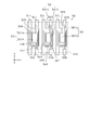
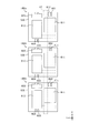
- FIG. 5 is a diagram in which a plurality of semiconductor modules shown in FIG. 1 are arranged side by side.
- FIG. 6 is a cross-sectional view showing the element structure of the semiconductor element in the semiconductor module shown in FIG. FIG.
- FIG. 7 is a schematic view of an electric power steering system to which the semiconductor module according to the first embodiment is applied.
- FIG. 8 is a diagram showing a drive circuit of an electric power steering system to which the semiconductor module shown in FIG. 1 can be applied.
- FIG. 9 is a plan view showing a semiconductor module according to a modified example.
- FIG. 10 is a plan view showing a semiconductor module according to a modified example.
- FIG. 11 is a plan view showing a semiconductor module according to a modified example.
- FIG. 12 is a plan view showing the semiconductor module according to the second embodiment.
- FIG. 13 is a plan view showing a state in which the resin mold is removed in the semiconductor module shown in FIG.
- FIG. 14 is a sectional view taken along line XIV-XIV of FIG. FIG.
- FIG. 15 is a cross-sectional view taken along the line XV-XV of FIG.
- FIG. 16 is a diagram in which a plurality of semiconductor modules shown in FIG. 12 are arranged side by side.
- FIG. 17 is a plan view showing a semiconductor module according to a modified example.
- FIG. 18 is a plan view showing a semiconductor module according to a modified example.
- FIG. 19 is a plan view showing a semiconductor module according to a modified example.
- FIG. 20 is a plan view showing the semiconductor module according to the third embodiment.
- FIG. 21 is a plan view showing a state in which the resin mold is removed in the semiconductor module shown in FIG.
- FIG. 22 is a sectional view taken along line XXII-XXII of FIG. FIG.
- FIG. 23 is a sectional view taken along line XXIII-XXIII of FIG.
- FIG. 24 is a diagram in which a plurality of semiconductor modules shown in FIG. 20 are arranged side by side.
- FIG. 25 is a plan view showing a semiconductor module according to a modified example.
- FIG. 26 is a plan view showing a semiconductor module according to a modified example.
- FIG. 27 is a plan view showing a semiconductor module according to a modified example.
- FIG. 28 is a plan view showing the semiconductor module according to the fourth embodiment.
- FIG. 29 is a plan view showing a state in which the resin mold is removed in the semiconductor module shown in FIG. 28.
- FIG. 30 is a sectional view taken along line XXII-XXII of FIG. 28.
- FIG. 31 is a diagram in which a plurality of semiconductor modules shown in FIG. 28 are arranged side by side.
- FIG. 32 is a plan view showing the semiconductor module according to the fifth embodiment.
- FIG. 33 is a plan view showing a state in which the resin mold is removed in the semiconductor module shown in FIG. 32.
- FIG. 34 is a diagram in which a plurality of semiconductor modules shown in FIG. 32 are arranged side by side.
- FIG. 35 is a diagram showing a drive circuit of an electric power steering system to which the semiconductor module shown in FIG. 32 can be applied.
- FIG. 36 is a plan view showing the semiconductor module according to the sixth embodiment.
- FIG. 37 is a plan view showing a state in which the resin mold is removed in the semiconductor module shown in FIG. 36.
- FIG. 38 is a sectional view taken along line XXXVIII-XXXVIII of FIG.
- FIG. 39 is a cross-sectional view taken along the line XXXIV-XXXIV of FIG.
- FIG. 40 is a diagram in which a plurality of semiconductor modules shown in FIG. 36 are arranged side by side.
- FIG. 41 is a diagram in which a set of semiconductor modules shown in FIG. 40 and another set of semiconductor modules are installed so as to be line-symmetrical on a wiring board.
- FIG. 42 is a diagram in which one set of semiconductor modules shown in FIG. 40 and another set of semiconductor modules are installed so as to be point-symmetrical on the wiring board.
- FIG. 43 is a diagram in which a plurality of semiconductor modules shown in FIG. 36 are arranged side by side.
- FIG. 44 is a diagram in which a plurality of semiconductor modules shown in FIG. 36 are arranged side by side.
- FIG. 45 is a diagram showing a mounting example of the semiconductor module according to the sixth embodiment.
- FIG. 46 is a diagram showing a mounting example of the semiconductor module according to the sixth embodiment.
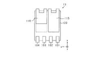
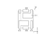
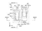
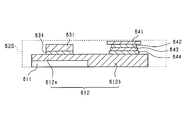
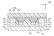
- the first semiconductor element 133 and the second semiconductor element 143 and the first semiconductor element 133 and the second semiconductor element 143 are integrally sealed. It includes a resin mold 120, conductive members 101 to 104, and conductive members 111, 112, 131, 141.
- the x-direction and the y-direction shown in FIGS. 1 to 5 are lateral to the semiconductor module 10, and the xy plane direction is the plane direction of the semiconductor module 10.
- the z direction is a vertical direction orthogonal to the plane direction.
- the semiconductor module 10 has four external terminals protruding in the negative direction of the y-axis from the resin mold 120 having a substantially rectangular shape when viewed from above, and is in the positive direction of the y-axis.
- the two external terminals have a protruding appearance.
- the four external terminals are a part of the conductive members 101 to 104 exposed from the resin mold 120, and the two external terminals are a part of the conductive members 111 and 112 exposed from the resin mold 120.
- the conductive member 112 includes a low-stage portion 112a that is not exposed from the resin mold 120 and a high-stage portion 112b that is exposed from the resin mold 120.
- the resin mold 120 is composed of a high heat dissipation resin material in which a resin material such as epoxy resin is mixed with a filler or the like for improving heat dissipation.
- a resin material such as epoxy resin
- a filler or the like for improving heat dissipation.
- a composite oxide material having high thermal conductivity such as alumina is selected.
- the thermal conductivity of the resin mold 120 can be adjusted by adjusting the type of filler and the filling rate.
- FIGS. 2 to 4 illustrate each configuration in the resin mold 120 of the semiconductor module 10.
- the positions where the resin mold 120 is provided are shown by broken lines.
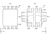
- the first semiconductor element 133 and the second semiconductor element 143 are integrally sealed in a state of being arranged side by side in the x direction in the same direction. ..
- the first semiconductor element 133 and the second semiconductor element 143 are semiconductor elements having the same structure, shape, size, and the like, and are substantially rectangular when viewed from above.
- the gate pad 136 of the first semiconductor element 133 and the gate pad 146 of the second semiconductor element 143 are provided at the same position in each semiconductor element.
- the first semiconductor element 133 and the second semiconductor element 143 are arranged substantially parallel to each other in the same direction as the adjacent semiconductor element and to the adjacent semiconductor element.
- the first semiconductor element 133 and the second semiconductor element 143 are vertical insulated gate semiconductor elements having an element structure as shown in FIG. More specifically, it is a power MOSFET (Metal-Oxide-Semiconductor Field-Effective Transistor: MOSFET).
- MOSFET Metal-Oxide-Semiconductor Field-Effective Transistor: MOSFET
- the first semiconductor element 133 and the second semiconductor element 143 include a semiconductor substrate 60, a source electrode 71, and a drain electrode 72.
- the source electrode 71 is formed in contact with the upper surface 60u of the semiconductor substrate 60.
- the drain electrode 72 is formed in contact with the lower surface 60b of the semiconductor substrate 60.
- the upper surface 60u corresponds to the first surface
- the lower surface 60b corresponds to the second surface.
- the n + region 61, the n ⁇ region 62, and the p + region 63 are laminated on the semiconductor substrate 60 in this order from the lower surface 60b side.
- An n + region 64 is formed on a part of the upper surface side of the p + region 63.
- a trench 73 is formed from the upper surface 60u of the semiconductor substrate 60, penetrating the n + region 64 and the p + region 63, and reaching the upper surface side of the n ⁇ region 62.
- a gate insulating film 74 is formed on the inner wall surface of the trench 73, and the trench 73 is filled with the gate electrode 75 in a state of being insulated from the semiconductor substrate 60 by the gate insulating film 74.
- the upper surface of the gate electrode 75 is covered with an insulating film 76, and the gate electrode 75 and the source electrode 71 are insulated by the insulating film 76.
- the material of the semiconductor substrate 60 is not particularly limited, and examples thereof include silicon (Si), silicon carbide (SiC), and gallium nitride (GaN).
- the source electrode 71 corresponds to the first electrode, and among the external terminals, the source terminal electrically connected to the source electrode 71 corresponds to the first terminal.
- the drain electrode 72 corresponds to the second electrode, and among the external terminals, the drain terminal electrically connected to the drain electrode 72 corresponds to the second terminal.
- the first semiconductor element 133 and the second semiconductor element 143 are viewed from above with the source electrode 71 facing upward (positive direction of the z-axis) and the drain electrode facing downward (negative direction of the z-axis), respectively.
- the case is arranged so that the longitudinal direction is the y direction.
- the conductive member 131 includes a beam-shaped portion 131a, a pad portion 131b, and a columnar portion 131c.
- the pad portion 131b is located on the upper surface side of the first semiconductor element 133, and is a substantially rectangular portion having a size of the upper surface similar to that of the first semiconductor element 133.
- the beam-shaped portion 131a extends in the negative direction of the y-axis along the long side of the upper surface of the substantially rectangular shape of the pad portion 131b, and extends above the conductive member 102.
- the columnar portion 131c extends downward from the beam-shaped portion 131a, and its lower end surface is joined to the upper surface of the conductive member 102 via the joining member 135.
- the conductive member 101 is electrically connected to the gate pad 136 by the gate wiring 137.
- the conductive member 141 includes a beam-shaped portion 141a, a pad portion 141b, and a columnar portion 141c.
- the pad portion 141b is located on the upper surface side of the second semiconductor element 143, and is a substantially rectangular portion having a size of the upper surface similar to that of the second semiconductor element 143.
- the beam-shaped portion 141a extends in the negative direction of the y-axis along the long side of the upper surface of the substantially rectangular shape of the pad portion 141b, and extends above the conductive member 104.
- the columnar portion 141c extends downward from the beam-shaped portion 141a, and its lower end surface is joined to the upper surface of the conductive member 104 via the joining member 145.
- the conductive member 103 is electrically connected to the gate pad 146 by the gate wiring 147.
- the gate wirings 137 and 147 are so-called clips, but wire bonding, wire ribbons, and the like may be used in addition to the clips.
- the conductive members 101 and 102 correspond to the gate terminal and the source terminal of the first semiconductor element 133, and the conductive member 111 corresponds to the drain pad of the first semiconductor element 133.
- the conductive members 103 and 104 correspond to the gate terminal and the source terminal of the second semiconductor element 143, and the conductive member 112 corresponds to the drain pad of the second semiconductor element 143.
- the high step portion 112b of the conductive member 112 is exposed from the resin mold 120, while the low step portion 112a is not exposed from the resin mold 120. Therefore, when the semiconductor module 10 is viewed from the bottom, the portion exposed from the resin mold 120 of the drain pad (conductive member 112) of the second semiconductor element 143 is the resin mold 120 of the drain pad (conductive member 111) of the first semiconductor element 133. The area is smaller than the part exposed from. Between the exposed high step portion 112b and the conductive members 103 and 104, there is a region where nothing is exposed on the surface of the resin mold 120 because the low step portion 112a is covered with the resin mold 120. This area corresponds to the common wiring area.
- the lower portion 112a and the lower of the conductive members 111 are located between the long sides facing in the x direction. There is a region including a portion adjacent to the step portion 112a. Therefore, as shown in FIG. 5, when the three semiconductor modules 10 are arranged side by side in the same direction in the x direction so as to be substantially orthogonal to the long side facing the x direction, the region A1 that travels straight in a strip shape along the x direction. Can be secured.
- reference numbers of 10a, 10b, and 10c are assigned in order from the positive direction side of the x-axis at the arrangement position.
- the region A1c shown in FIG. 5 indicates the common wiring region A1c of the semiconductor module 10c.
- the common wiring region A1c is a strip-shaped region that travels substantially straight from one opposite side to the other on the surface of the resin mold 120 on which the conductive member 111 is exposed.
- the conductive member 111 exists in the common wiring region A1c, and no conductive member (conductive member 112 or the like) other than the conductive member 111 exists.
- the semiconductor modules 10a and 10b also have the same common wiring area as the common wiring area A1c.
- the width of the common wiring area A1c in the direction orthogonal to the wiring direction (x direction) is such that the wiring can be installed. For example, the installation intervals of the conductive members 101 to 104 (intervals in the x direction). ) Wider.
- Region A1 is included in a region connecting the common wiring region of the semiconductor modules 10a to 10c and the region between them. This region A1 extends over three semiconductor modules 10a, 10b, and 10c, and in the region A1, only the conductive member 111 is exposed from the resin mold 120. Therefore, by installing common wiring for connecting to the three conductive members 111 included in the three semiconductor modules 10a, 10b, and 10c in the region A1, the three conductive members 111 are electrically connected to each other. Can be done.
- the wiring width of the common wiring (width in the y direction orthogonal to the x direction, which is the wiring direction) is wider than the wiring width (width in the x direction) of the conductive members 101 to 104, and the width of the region A1 in the y direction is , The width that can install common wiring is secured.
- the conductive members 101 to 104, 111, 112 are exposed from the resin mold 120 on the upper surface side or the lower surface side of the semiconductor module 10.
- the conductive member 111 corresponds to the common wiring electrode
- the conductive members 101 to 104, 112 correspond to the non-common wiring electrode.
- the common wiring electrode is exposed from the resin mold 120 on the upper surface side (positive direction side of the z-axis) or the lower surface side (negative direction side of the z-axis) of the semiconductor module 10, and is the first electrode (source electrode 71) and the first electrode. It is an electrode that is electrically connected to at least one of the two electrodes (drain electrode 72).
- the common wiring electrode is connected to the common wiring when the semiconductor module 10 is connected to another semiconductor module by the common wiring.
- common wiring can be installed from one side facing the x-axis direction to the other side.
- the semiconductor module 10 when the common wiring is connected to the common wiring electrode (conductive member 111), the common wiring is not electrically connected to the non-common wiring electrode (conductive members 101 to 104, 112).
- Each configuration (plurality of semiconductor elements, a plurality of conductive members, etc.) constituting the semiconductor module 10 allows common wiring to be installed from one opposite side to the other side on the surface of the resin mold on which the electrodes are exposed. Have been placed. Therefore, the plurality of semiconductor modules 10 can be electrically connected to each other on the lower surface side of the semiconductor module 10. As a result, the wiring space on the side of the semiconductor module 10 can be reduced, which can contribute to the miniaturization of the mounting board.
- the resin mold 120 is made of a high heat dissipation resin material, heat dissipation of the semiconductor module 10 can be promoted via the resin mold 120.
- the semiconductor module 10 can be applied to the drive circuit of the electric power steering system (EPS) 80 of the vehicle as shown in FIG.
- the EPS 80 includes a steering wheel 90, a steering shaft 91, a pinion gear 92, a rack shaft 93, and an EPS device 81 that form a steering wheel.
- a steering shaft 91 is connected to the steering wheel 90.
- a pinion gear 92 is provided at the tip of the steering shaft 91.
- the pinion gear 92 meshes with the rack shaft 93.
- Wheels 95 are rotatably connected to both ends of the rack shaft 93 via a tie rod or the like.
- the EPS device 81 includes a torque sensor 94, a speed reducer 96, a rotary electric machine 82, and an energization circuit unit 83.
- the torque sensor 94 is provided on the steering shaft 91 and detects the steering torque Trq, which is the output torque of the steering shaft 91.
- the rotary electric machine 82 generates an auxiliary torque according to the detected steering torque Trq and the steering direction of the steering wheel 90.
- the energizing circuit unit 83 controls the drive of the rotary electric machine 82.
- the speed reducer 96 transmits auxiliary torque to the steering shaft 91 while decelerating the rotation of the rotation shaft of the rotor of the rotary electric machine 82.
- the stator of the rotary electric machine 82 includes a first winding group M1 and a second winding group M2.
- the first winding group M1 includes a star-shaped first U-phase winding U1, a first V-phase winding V1, and a first W-phase winding W1, and the second winding group M2 has a star-shaped connection. It includes a 2U phase winding U2, a second V phase winding V2, and a second W phase winding W2.
- the first ends of the first U, V, W phase windings U1, V1, W1 are connected at a neutral point.
- the first U, V, W phase windings U1, V1, W1 are deviated by 120 ° at the electric angle ⁇ e.
- the first ends of the second U, V, W phase windings U2, V2, W2 are connected at a neutral point.
- the second U, V, and W phase windings U2, V2, and W2 are deviated by 120 ° at the electric angle ⁇ e.
- the energization circuit unit 83 includes a first inverter INV1 and a second inverter INV2 as power converters, and a first relay RL1 and a second relay RL2 as power relays.
- the second end of the first U phase winding U1 is connected to the connection point between the upper arm switch SU1p and the lower arm switch SU1n of the first U phase.
- the second end of the first V phase winding V1 is connected to the connection point between the upper arm switch SV1p of the first V phase and the lower arm switch SV1n.
- the second end of the first W phase winding W1 is connected to the connection point between the upper arm switch SW1p of the first W phase and the lower arm switch SW1n.
- the second end of the second U-phase winding U2 is connected to the connection point between the upper arm switch SU2p and the lower arm switch SU2n of the second U phase.
- the second end of the second V-phase winding V2 is connected to the connection point between the upper arm switch SV2p and the lower arm switch SV2n of the second V phase.
- the second end of the second W phase winding W2 is connected to the connection point between the upper arm switch SW2p and the lower arm switch SW2n of the second W phase.
- the high potential side terminals of the upper arm switches SU1p, SV1p, SW1p of the first U, V, W phases are connected to the positive electrode terminal of the battery 97, which is a DC power supply, via the first relay RL1.
- the low potential side terminals of the lower arm switches SU1n, SV1n, SW1n of the first U, V, W phase are connected to the ground via the resistors RU1, RV1, RW1.
- the high potential side terminals of the upper arm switches SU2p, SV2p, SW2p of the second U, V, W phase are connected to the positive electrode terminal of the battery 97 via the second relay RL2.
- the low potential side terminals of the lower arm switches SU2n, SV2n, SW2n of the second U, V, W phase are connected to the ground via the resistors RU2, RV2, RW2.
- the negative electrode terminal of the battery 97 is connected to the ground.
- MOSFETs as exemplified in the first semiconductor element 133 and the second semiconductor element 143 can be used.
- Two switches SU1p and SU1n, SV1p and SV1n, SW1p and SW1n, SU2p and SU2n, SV2p and SV2n, SW2p and SW2n, which are connected in series in each arm, are the source electrode of the former MOSFET and the drain of the latter MOSFET, respectively.
- the electrodes are connected and connected in series.
- Semiconductor modules SU1, SV1, SW1, SU2 that integrate two switches SU1p and SU1n, SV1p and SV1n, SW1p and SW1n, SU2p and SU2n, SV2p and SV2n, and SW2p and SW2n connected in series in each arm.
- the semiconductor module 10 can be used as the SV2 and SW2.
- the semiconductor module 10 can be applied to the first inverter INV1 and the second inverter INV2 to form an inverter circuit.
- MOSFETs as exemplified in the first semiconductor element 133 and the second semiconductor element 143 can be used.
- the switches SP1 and SP2 are power relay switches, and the switches SC1 and SC2 are reverse connection protection relays.
- the two switches SP1 and SC1, SP2 and SC2, which are connected in series in each arm, are connected in series by connecting the source electrodes of the MOSFETs to each other.
- the energization circuit unit 83 detects the current flowing through the resistors RU1, RV1, RW1 and outputs the currents as the first U, V, W phase currents Iur1, Ivr1, Iwr1. Further, the current flowing through the RU2, RV2, and RW2 is detected and output as the second U, V, and W phase currents Iur2, Ivr2, and Iwr2.
- the energization circuit unit 83 includes an ECU mainly composed of a microcomputer, and the ECU operates each switch of the first inverter INV1 and the second inverter INV2 in order to control the torque of the rotary electric machine 82 to the torque command value Tr *. To do.
- the torque command value Tr * is set based on, for example, the steering torque Trq detected by the torque sensor 94.
- the energization circuit unit 83 calculates the electric angle ⁇ e of the rotary electric machine 82 based on the output signal of the angle sensor by the ECU.
- an angle sensor for example, an angle sensor including a magnet which is a magnet generating portion provided on the rotor side of the rotary electric machine 82 and a magnetic detection element provided close to the magnet can be exemplified. ..
- the functions provided by the above-mentioned ECU can be provided, for example, by software recorded in a substantive memory device and a computer, hardware, or a combination thereof that executes the software.
- the semiconductor module 10 can be applied to the EPS 80, and can be applied to the energization circuit unit 83 corresponding to the drive circuit of the EPS 80 as the semiconductor modules SU1 to SW2 including two switches connected in series. it can.
- the semiconductor module 10 can be applied to the inverter circuits shown as the first inverter INV1 and the second inverter INV2, respectively, and the first semiconductor element 133 and the second semiconductor element 143 are connected in series, respectively. It is applied to inverter circuits as a switching element.
- the semiconductor module 10 As shown in FIG. 1A, as the semiconductor module 10, the conductive members 131 and 141 have been described by way of example when they are not exposed from the resin mold 120, but the present invention is not limited to this. Like the semiconductor module 11 shown in FIG. 9, the semiconductor module 11 may be provided with conductive members 151 and 161 protruding from the resin mold 120 on the upper surface side thereof. Since the other configurations of the semiconductor module 11 are the same as those of the semiconductor module 10, the description thereof will be omitted.
- the conductive members 111 and 112 extend beyond the positive direction of the y-axis of the resin mold 120 by way of example, but the present invention is not limited to this.
- the resin mold 120 may include conductive members 113 and 114 that do not exceed the positive direction of the y-axis. Since the other configurations of the semiconductor module 12 are the same as those of the semiconductor module 10, the description thereof will be omitted.
- the resin mold 120 may include conductive members 115 and 116 in which a portion extending beyond the positive direction of the y-axis is branched into two. .. Since the other configurations of the semiconductor module 13 are the same as those of the semiconductor module 10, the description thereof will be omitted.
- first semiconductor element 133 first semiconductor element 133, second semiconductor element 143
- the semiconductor elements may be arranged substantially point-symmetrically with the adjacent semiconductor elements in the opposite direction to the adjacent semiconductor elements.
- the second semiconductor element 243 has a vertical direction (z direction) with respect to the first semiconductor element 233. It is integrally sealed in a state where it is arranged side by side in the x-axis direction in a direction rotated by 180 ° to the center. That is, the first semiconductor element 233 and the second semiconductor element 243 are arranged substantially point-symmetrically with the adjacent semiconductor elements in the opposite directions to the adjacent semiconductor elements.
- the first semiconductor element 233 and the second semiconductor element 243 are semiconductor elements having the same structure, shape, size, and the like. The material, shape, size, and the like of each configuration included in the semiconductor module 20 are the same as those of each configuration included in the semiconductor module.
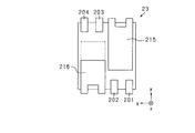
- each configuration on the first semiconductor element 233 side that is, the conductive member 231 and the joining member 232, the first semiconductor element 233, the joining member 234, and the conductive member 211 are the first in the first embodiment. 1 Since the semiconductor elements are arranged in the same manner as each configuration on the 133 side, the description will be omitted by replacing the reference number in the 100s with the 200s.
- the conductive member 241 and the joining member 242, the second semiconductor element 243, the joining member 244, and the conductive member 212 are upward as in the first embodiment. It is arranged in this order from.
- the conductive member 241 includes a beam-shaped portion 241a, a pad portion 241b, and a columnar portion 241c.
- the beam-shaped portion 241a extends in the positive direction of the y-axis along the long side of the upper surface of the substantially rectangular shape of the pad portion 241b, and extends above the conductive member 203.
- the columnar portion 241c extends downward from the beam-shaped portion 241a, and its lower end surface is joined to the upper surface of the conductive member 203 via the joining member 245.
- the conductive member 204 is electrically connected to the gate pad 246 by the gate wiring 247.
- the conductive members 201 and 202 correspond to the gate terminal and the source terminal of the first semiconductor element 233, and the conductive member 211 corresponds to the drain pad of the first semiconductor element 233.
- the conductive members 203 and 204 correspond to the source terminal and the gate terminal of the second semiconductor element 243, and the conductive member 212 corresponds to the drain pad of the second semiconductor element 243.
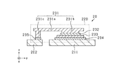
- the high step portion 212b of the conductive member 212 is exposed from the resin mold 220, while the low step portion 212a is not exposed from the resin mold 220. Therefore, when the semiconductor module 20 is viewed from the bottom, the portion exposed from the resin mold 220 of the drain pad (conductive member 212) of the second semiconductor element 243 is the resin mold 220 of the drain pad (conductive member 211) of the first semiconductor element 233. The area is smaller than the part exposed from. Between the exposed high step portion 212b and the conductive members 203 and 204, there is a region where nothing is exposed on the surface of the resin mold 220 because the low step portion 212a is covered with the resin mold 220. This area corresponds to the common wiring area.
- the lower portion 212a and the lower of the conductive members 211 are located between the long sides facing in the x direction.
- a portion adjacent to the step portion 212a is included. Therefore, as shown in FIG. 16, when the three semiconductor modules 20 are arranged side by side in the same direction in the x direction so as to be substantially orthogonal to the long side facing the x direction, the region A2 that travels straight in a strip shape along the x direction. Can be secured.
- reference numbers of 20a, 20b, and 20c are assigned in order from the positive direction side of the x-axis at the arrangement position.
- the common wiring region A2c is a strip-shaped region that travels substantially straight from one opposite side to the other on the surface of the resin mold 220 on which the conductive member 211 is exposed.
- the conductive member 211 exists in the common wiring region A2c, and no conductive member other than the conductive member 211 exists.
- the semiconductor modules 20a and 20b also have the same common wiring area as the common wiring area A2c.
- Region A2 is included in a region connecting the common wiring region of the semiconductor modules 20a to 20c and the region between them. This region A2 extends over three semiconductor modules 20a, 20b, and 20c, and in the region A2, only the conductive member 211 is exposed from the resin mold 220. Therefore, by installing common wiring for connecting to the three conductive members 211 included in the three semiconductor modules 20a, 20b, and 20c in the region A2, the three conductive members 211 are electrically connected to each other. Can be done.
- the conductive members 201 to 204, 211,212 are exposed from the resin mold 220 on the upper surface side or the lower surface side of the semiconductor module 20.
- the conductive member 211 corresponds to the common wiring electrode
- the conductive members 201 to 204, 212 correspond to the non-common wiring electrode.
- the bottom surface of the resin mold 220 is in the x direction without being electrically connected to the electrodes for non-common wiring (conductive members 201 to 204, 212).
- Common wiring can be installed from one side facing the other side to the other side.
- the wiring width of the common wiring (width in the y direction orthogonal to the x direction, which is the wiring direction) is wider than the wiring width (width in the x direction) of the conductive members 201 to 204, and the width of the region A2 in the y direction is , The width that can install common wiring is secured.
- the common wiring electrode is exposed without being electrically connected to the non-common wiring electrode.
- Each configuration (a plurality of semiconductor elements, a plurality of conductive members, etc.) constituting the semiconductor module 20 is arranged so that the common wiring can be installed from one opposite side to the other side on the surface of the resin mold. .. Therefore, the plurality of semiconductor modules 20 can be electrically connected to each other on the lower surface side of the semiconductor module 20. As a result, the wiring space on the side of the semiconductor module 20 can be reduced, which can contribute to the miniaturization of the mounting board.
- the resin mold 220 is made of a high heat dissipation resin material, heat dissipation of the semiconductor module 20 can be promoted via the resin mold 220.
- the semiconductor module 20 can be applied to the EPS 80 in the same manner as the semiconductor module 10, and is a semiconductor module SU1 to SW2 including two switches connected in series, and is an energization circuit unit 83 corresponding to the drive circuit of the EPS 80. Can be applied to.
- the semiconductor modules 21 to 23 shown in FIGS. 17 to 19 can be applied as modification examples.
- the conductive members 251,261 protruding from the resin mold 220 may be provided instead of the conductive members 231,241.
- the conductive members 213 and 214 that do not exceed the positive direction of the y-axis of the resin mold 220 may be provided.
- the resin mold 220 may include conductive members 215 and 216 in which a portion extending beyond the positive direction of the y-axis is branched into two. .. Since the other configurations of the semiconductor modules 21 to 23 are the same as those of the semiconductor module 20, the description thereof will be omitted.
- the plurality of semiconductor elements are arranged side by side in the direction (y direction) in which the conductive member protrudes as an external terminal (x direction), but the external terminals are arranged. They may be arranged side by side in the protruding direction.
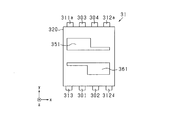
- the second semiconductor element 343 has a vertical direction (z direction) with respect to the first semiconductor element 333. It is integrally sealed in a state where it is arranged side by side in the y direction in a direction rotated by 180 ° to the center. That is, the first semiconductor element 333 and the second semiconductor element 343 are arranged substantially point-symmetrically with the adjacent semiconductor elements in the opposite directions to the adjacent semiconductor elements. As in the first embodiment, the first semiconductor element 333 and the second semiconductor element 343 are semiconductor elements having the same structure, shape, size, and the like. The first semiconductor element 333 and the second semiconductor element 343 are arranged so that the longitudinal direction when viewed from above is parallel to the x-axis.
- the conductive member 331 includes a beam-shaped portion 331a, a pad portion 331b, and a columnar portion 331c.
- the beam-shaped portion 331a extends in the positive direction of the x-axis along the long side of the upper surface of the substantially rectangular shape of the pad portion 331b, and extends above the conductive member 312.
- the columnar portion 331c extends downward from the beam-shaped portion 331a, and its lower end surface is joined to the upper surface of the conductive member 312 via a joining member (not shown).
- the conductive member 304 is electrically connected to the gate pad 346 by the gate wiring 347.
- the conductive member 341 includes a beam-shaped portion 341a, a pad portion 341b, and a columnar portion 341c.
- the beam-shaped portion 341a extends in the negative direction of the x-axis along the long side of the upper surface of the substantially rectangular shape of the pad portion 341b, and extends above the conductive member 313.
- the columnar portion 341c extends downward from the beam-shaped portion 341a, and its lower end surface is joined to the upper surface of the conductive member 313 via a joining member (not shown).
- the conductive member 301 is electrically connected to the gate pad 346 by the gate wiring 347.
- the conductive member 311 has a substantially L-shape, and includes a terminal portion 311a and an element installation portion 311b.
- the first semiconductor element 333 is installed in the element installation portion 311b.
- the terminal portion 311a extends from the element installation portion 311b in the positive direction of the y-axis and extends beyond the end portion of the resin mold 320 on the positive direction side of the y-axis.
- the conductive member 312 includes a first terminal portion 312a, a lower stage portion 312b, an element installation portion 312c, and a second terminal portion 312d.
- the second semiconductor element 343 is installed in the element installation unit 312c.
- the lower step portion 312b and the first terminal portion 312a are elongated strip-shaped and substantially rectangular portions extending from the end portion of the element installation portion 312c on the positive direction side of the x-axis to the positive direction side of the y-axis, and the lower stage portion 312b. Is closer to the element installation portion 312c.
- the second terminal portion 312d is a strip-shaped and substantially rectangular portion extending from the end portion of the element installation portion 312c on the positive direction side of the x-axis to the negative direction side of the y-axis.
- the conductive member 312 is in contact with the drain electrode of the second semiconductor element 343 via the joining member 344 in the element installation portion 312c and is electrically connected. Further, the conductive member 312 is electrically connected to the source electrode of the first semiconductor element 333 at the lower stage portion 312b via the conductive member 331, the joining member 332, and the like. That is, the conductive member 312 joins the first electrode (source electrode) of the first semiconductor element 333 and the second electrode (drain electrode) of the second semiconductor element 343 arranged adjacent to the first semiconductor element 333. Corresponds to the joint conductive member to be formed.
- the conductive member 313 has an elongated strip shape and a substantially rectangular shape, from the end portion of the element installation portion 312c of the conductive member 312 on the positive direction side of the y-axis to beyond the end portion of the resin mold 320 on the negative direction side of the y-axis. It is postponed.
- the conductive members 304 and 312 correspond to the gate terminal and the source terminal of the first semiconductor element 333, and the conductive member 311 corresponds to the drain pad of the first semiconductor element 333.
- the conductive members 301 and 313 correspond to the gate terminal and the source terminal of the second semiconductor element 343, and the conductive member 312 corresponds to the drain pad of the second semiconductor element 343.
- the first terminal portion 312a, the element installation portion 312c, and the second terminal portion 312d of the conductive member 312 correspond to the high-stage portion and are exposed from the resin mold 320 while being exposed.
- the lower step 312b is not exposed from the resin mold 320. Therefore, when the semiconductor module 30 is viewed from the bottom, it seems that the first terminal portion 312a and the element mounting portion 312c are not connected, while the second terminal portion 312d and the element mounting portion 312c are connected.
- the lower step portion 312b is adjacent to a part of the element installation portion 311b of the conductive member 311 in the x direction.
- the lower step portion 312b is covered with the resin mold 320 between the exposed first terminal portion 312a and the element installation portion 312c, so that nothing is exposed on the surface of the resin mold 320.
- the lower step portion 312b and the element of the conductive member 311 are installed between the long sides facing in the x direction.
- a portion of the portion 311b adjacent to the lower portion 312b is included. Therefore, as shown in FIG. 24, when the three semiconductor modules 30 are arranged side by side in the same direction in the x direction so as to be substantially orthogonal to the long side facing the x direction, the region A3 that goes straight in a band shape along the x direction. Can be secured.
- reference numbers of 30a, 30b, and 30c are assigned in order from the positive direction side of the x-axis at the arrangement position.
- the region A3c shown in FIG. 24 indicates the common wiring region A3c of the semiconductor module 30c.
- the common wiring region A3c is a strip-shaped region that travels substantially straight from one opposite side to the other on the surface of the resin mold 320 on which the conductive member 311 is exposed.
- the conductive member 311 exists in the common wiring region A3c, and no conductive member other than the conductive member 311 exists.
- the semiconductor modules 30a and 30b also have the same common wiring area as the common wiring area A3c.
- Region A3 is included in the region connecting the common wiring region of the semiconductor modules 30a to 30c and the region between them. This region A3 extends over three semiconductor modules 30a, 30b, and 30c, and in the region A3, only the conductive member 311 (more specifically, the element mounting portion 311b) is exposed from the resin mold 320. Therefore, by installing common wiring for connecting to the three conductive members 311 included in the three semiconductor modules 30a, 30b, and 30c in the region A3, the three conductive members 311 are electrically connected to each other. Can be done.
- the conductive members 301 to 304 and 311 to 313 are exposed from the resin mold 320 on the upper surface side or the lower surface side of the semiconductor module 30.
- the conductive member 311 corresponds to the common wiring electrode
- the conductive members 301 to 304, 312, 313 correspond to the non-common wiring electrode.
- each configuration (a plurality of semiconductor elements, a plurality of conductive members, etc.) constituting the semiconductor module 30 is arranged so that the common wiring can be installed from one opposite side to the other side on the surface of the resin mold. ing. Therefore, the plurality of semiconductor modules 30 can be electrically connected to each other on the lower surface side of the semiconductor module 30. As a result, the wiring space on the side of the semiconductor module 30 can be reduced, which can contribute to the miniaturization of the mounting board.
- the resin mold 320 is made of a high heat dissipation resin material, heat dissipation of the semiconductor module 30 can be promoted via the resin mold 320.
- the semiconductor module 30 can be applied to the EPS 80 in the same manner as the semiconductor module 10, and is a semiconductor module SU1 to SW2 including two switches connected in series, and is an energization circuit unit 83 corresponding to the drive circuit of the EPS 80. Can be applied to.
- the semiconductor modules 31 to 33 shown in FIGS. 25 to 27 can be applied as a modification.
- the conductive members 351 and 361 protruding from the resin mold 320 may be provided on the upper surface side thereof instead of the conductive members 331 and 341.
- a conductive member 305 in which these are integrated may be provided.
- a conductive member 306 that integrates these members may be provided.
- the conductive member 305 is a gate terminal of the first semiconductor element 333
- the conductive member 306 is a gate terminal of the second semiconductor element 343.
- one of the conductive members 301 and 302 may not be provided.
- one of the conductive members 303 and 304 may not be provided.
- the semiconductor module 33 is not provided with the conductive members 301 and 303. On the contrary, since the other configurations of the semiconductor modules 31 to 33 are the same as those of the semiconductor module 30, the description thereof will be omitted.
- the conductive member 112 corresponding to the non-common wiring electrode includes a high step portion 112b that is higher toward the lower surface side exposed from the resin mold 120 and a lower step portion 112a that is lower than the high step portion 112b. This allows common wiring, but is not limited to this.
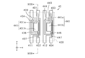
- the first semiconductor element 433 and the second semiconductor element 443 are arranged side by side in the x direction in the same direction in the resin mold 420. It is integrally sealed in the closed state. That is, the first semiconductor element 433 and the second semiconductor element 443 are arranged substantially parallel to each other in the same direction as the adjacent semiconductor element and to the adjacent semiconductor element. As in the first embodiment, the first semiconductor element 433 and the second semiconductor element 443 are semiconductor elements having the same structure, shape, size, and the like. The first semiconductor element 433 and the second semiconductor element 443 are arranged so that the longitudinal direction when viewed from above is parallel to the x-axis.
- the conductive member 431, the joining member 432, the first semiconductor element 433, the joining member 434, and the conductive member 411 are located above, as in the first embodiment. It is arranged in this order from.
- the conductive member 431 includes a beam-shaped portion 431a, a pad portion 431b, and a columnar portion 431c.
- the beam-shaped portion 431a extends in the positive direction of the y-axis along the long side of the upper surface of the substantially rectangular shape of the pad portion 431b, and extends above the conductive member 412.
- the columnar portion 431c extends downward from the beam-shaped portion 431a, and its lower end surface is joined to the upper surface of the conductive member 401 via a joining member (not shown).
- the conductive member 402 is electrically connected to the gate pad 446 by the gate wiring 447.
- the conductive member 441 includes a beam-shaped portion 441a, a pad portion 441b, and a columnar portion 441c.
- the beam-shaped portion 441a extends in the positive direction of the y-axis along the long side of the upper surface of the substantially rectangular shape of the pad portion 441b, and extends above the conductive member 403.
- the columnar portion 441c extends downward from the beam-shaped portion 441a, and its lower end surface is joined to the upper surface of the conductive member 403 via a joining member (not shown).
- the conductive member 404 is electrically connected to the gate pad 446 by the gate wiring 447.
- Each configuration on the second semiconductor element 443 side is a state in which each configuration on the first semiconductor element 433 side is moved in the positive direction of the x-axis, and each configuration has the same shape, size, and positional relationship. There is.
- the conductive members 401 and 402 correspond to the source terminal and the gate terminal of the first semiconductor element 433, and the conductive member 411 corresponds to the drain pad of the first semiconductor element 433.
- the conductive members 403 and 404 correspond to the source terminal and the gate terminal of the second semiconductor element 243, and the conductive member 412 corresponds to the drain pad of the second semiconductor element 443.
- the conductive member 411 has a substantially T-shape, and includes a first terminal portion 411a, an element installation portion 411b, an intermediate portion 411c, and a second terminal portion 411d.
- the element installation portion 411b is provided substantially in the center of the conductive member 411 in the y direction, and the intermediate portion 411c is located on the negative direction side of the x-axis with respect to the element installation portion 411b.
- the first terminal portion 411a is provided on the positive direction side of the y-axis and extends beyond the end portion of the resin mold 420 on the positive direction side of the y-axis.
- the second terminal portion 411d is provided on the negative direction side of the y-axis and extends beyond the end portion of the resin mold 420 on the negative direction side of the y-axis.
- the intermediate portion 411c is a portion between the first terminal portion 411a and the second terminal portion 411d.
- the first semiconductor element 433 is installed in the element installation portion 411b. Since the shape of the conductive member 412 is the same as that of the conductive member 411, the description will be omitted by replacing 411 in the reference number with 412.
- the common wiring region A4c is a strip-shaped region that travels substantially straight from one opposite side to the other on the surface of the resin mold 420 on which the conductive member 411 is exposed.
- the conductive member 411 exists in the common wiring region A4c, and no conductive member other than the conductive member 411 exists.
- the semiconductor modules 40a and 40b also have the same common wiring area as the common wiring area A4c.
- Region A4 is included in a region connecting the common wiring region of the semiconductor modules 40a to 40c and the region between them.
- This region A4 extends over three semiconductor modules 40a, 40b, and 40c, and in the region A4, only the conductive member 411 is exposed from the resin mold 420. Therefore, by installing common wiring for connecting to the three conductive members 411 included in the three semiconductor modules 40a, 40b, and 40c in the region A4, the three conductive members 411 are electrically connected to each other. Can be done.
- the conductive member 412 in the resin mold 420 which is substantially rectangular when the semiconductor module 40 is viewed from the bottom, the conductive member is between the short sides facing in the y direction. There is a region that contains only 412. Therefore, common wiring connected to the three conductive members 412 included in the three semiconductor modules 40a, 40b, and 40c can be installed.
- the conductive members 401 to 404, 411, 412 are exposed from the resin mold 420 on the upper surface side or the lower surface side of the semiconductor module 40.
- the conductive members 411 and 412 correspond to the electrodes for common wiring
- the conductive members 401 to 404 correspond to the electrodes for non-common wiring.
- Common wiring can be installed from one side facing the x direction to the other side.
- the wiring width of the common wiring (width in the x direction orthogonal to the y direction, which is the wiring direction) is wider than the wiring width (width in the x direction) of the conductive members 401 to 404, and the width of the region A4 in the x direction is , The width that can install common wiring is secured.
- the common wiring electrode is not electrically connected to the non-common wiring electrode.
- Each configuration (a plurality of semiconductor elements, a plurality of conductive members, etc.) constituting the semiconductor module 40 can be installed so that the common wiring can be installed from one opposite side to the other side on the surface of the resin mold to which is exposed. Have been placed. Therefore, the plurality of semiconductor modules 40 can be electrically connected to each other on the lower surface side of the semiconductor module 40. As a result, the wiring space on the side of the semiconductor module 40 can be reduced, which can contribute to the miniaturization of the mounting board.
- the resin mold 420 is made of a high heat dissipation resin material, heat dissipation of the semiconductor module 40 can be promoted via the resin mold 420.
- the electrodes for common wiring extend to positions protruding from both of the pair of opposite sides of the surface of the resin mold. With this configuration, common wiring can be realized without providing a step in the thickness direction of the conductive member. Further, in the semiconductor module 40, since it is not necessary to separately make the conductive member on the first semiconductor element side and the conductive member on the second semiconductor element side, the configuration is simple and it can contribute to reduction of manufacturing cost and the like.
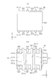
- the first semiconductor element 533, the second semiconductor element 543, and the third semiconductor element 553 have the same orientation in the resin mold 520. It is integrally sealed in a state where it is arranged side by side in the x direction.
- the semiconductor module 50 has a configuration in which a third semiconductor element 553 and a conductive member loaded or connected to the third semiconductor element 553 are further added to the semiconductor module 40. Since each configuration on the first semiconductor element 533 side and each configuration on the second semiconductor element 543 side are the same as each configuration on the first semiconductor element 433 side and each configuration on the second semiconductor element 443 side in the semiconductor module 40, The description will be omitted by replacing the reference number in the 400 series with the reference number in the 500 series.
- Each configuration on the third semiconductor element 553 side is a state in which each configuration on the first semiconductor element 533 side or each configuration on the second semiconductor element 543 side is moved in the positive direction of the x-axis, and each configuration has the same shape. , Size, and positional relationship.
- the conductive member 581 includes a beam-shaped portion 581a, a pad portion 581b, and a columnar portion (not shown).
- the beam-shaped portion 581a extends in the positive direction of the y-axis along the long side of the upper surface of the substantially rectangular shape of the pad portion 581b, and extends above the conductive member 505.
- the columnar portion extends downward from the beam-shaped portion 581a, and its lower end surface is joined to the upper surface of the conductive member 505 via a joining member (not shown).
- the conductive member 506 is electrically connected to the gate pad by a gate wiring.
- the conductive members 501 and 502 correspond to the source terminal and the gate terminal of the first semiconductor element 533, and the conductive member 511 corresponds to the drain pad of the first semiconductor element 533.
- the conductive members 503 and 504 correspond to the source terminal and the gate terminal of the second semiconductor element 543, and the conductive member 512 corresponds to the drain pad of the second semiconductor element 543.
- the conductive members 505 and 506 correspond to the source terminal and the gate terminal of the third semiconductor element 553, and the conductive member 571 corresponds to the drain pad of the third semiconductor element 553.
- the region A5c shown in FIG. 34 indicates the common wiring region A5c of the semiconductor module 50c.
- the common wiring region A5c is a strip-shaped region that travels substantially straight from one opposite side to the other on the surface of the resin mold 520 on which the conductive member 511 is exposed.
- the conductive member 511 exists in the common wiring region A5c, and no conductive member other than the conductive member 511 exists.
- the semiconductor modules 50a and 50b also have the same common wiring area as the common wiring area A5c.
- Region A5 is included in the region connecting the common wiring region of the semiconductor modules 50a to 50c and the region between them. This region A5 extends over three semiconductor modules 50a, 50b, and 50c, and in the region A5, only the conductive member 511 is exposed from the resin mold 520. Therefore, by installing common wiring for connecting to the three conductive members 511 included in the three semiconductor modules 50a, 50b, and 50c in the region A5, the three conductive members 511 are electrically connected to each other. Can be done.
- the wiring width of the common wiring (width in the x direction orthogonal to the y direction, which is the wiring direction) is wider than the wiring width (width in the x direction) of the conductive members 501 to 506, and the width of the region A5 in the x direction is , The width that can install common wiring is secured.
- the semiconductor module according to this embodiment can be used in a drive circuit as shown in FIG. 35.
- the drive circuit shown in FIG. 35 corresponds to a drive circuit shown in FIG. 8 to which the motor relay switches TU1, TV1, TW1, TU2, TV2, and TW2 are added.
- the connection point between the upper arm switch SU1p and the lower arm switch SU1n of the first U phase and the second end of the first U phase winding U1 are connected via the motor relay switch TU1.
- the connection point between the upper arm switch SV1p and the lower arm switch SV1n of the first V phase and the second end of the first V phase winding V1 are connected via the motor relay switch TV1.
- connection point between the upper arm switch SW1p and the lower arm switch SW1n of the first W phase and the second end of the first W phase winding U1 are connected via the motor relay switch TW1.
- the connection point between the upper arm switch SU2p and the lower arm switch SU2n of the second U phase and the second end of the second U phase winding U2 are connected via the motor relay switch TU2.
- the connection point between the upper arm switch SV2p and the lower arm switch SV2n of the second V phase and the second end of the second V phase winding V2 are connected via the motor relay switch TV2.
- the connection point between the upper arm switch SW2p and the lower arm switch SW2n of the second W phase and the second end of the second W phase winding U2 are connected via the motor relay switch TW2.
- the semiconductor module 50 can be applied to the EPS 80, and is applied to the energization circuit unit 83 corresponding to the drive circuit of the EPS 80 as the semiconductor modules SU1 to SW2 including two switches connected in series and a motor relay switch. be able to. Further, it may be configured as a semiconductor module in which SU1, SV1 and SW1 shown in FIG. 8 are integrated.
- the semiconductor module including the low-stage portion 112a and the high-stage portion 112b in the conductive member 112 corresponding to the non-common wiring electrode described in the first embodiment also includes three or more semiconductor elements.
- Common wiring can be made possible.
- a semiconductor including three semiconductor elements capable of common wiring by adding each configuration on the second semiconductor element 143 side to the semiconductor module 10 on the positive direction side of the x-axis. Modules can be realized.
- the semiconductor module 160 integrally seals the first semiconductor element 633 and the second semiconductor element 643 and the first semiconductor element 633 and the second semiconductor element 643. It includes a resin mold 620, conductive members 601 to 605, and conductive members 611, 612, 631, 641.
- the x-direction and the y-direction shown in FIGS. 36 to 39 are the sides of the semiconductor module 160, and the xy plane direction is the plane direction of the semiconductor module 160.
- the z direction is a vertical direction orthogonal to the plane direction.
- FIG. 36 (a) is a top view of the semiconductor module 160
- FIG. 36 (b) is a bottom view of the semiconductor module 160
- FIG. 37 is a top view of each configuration in the resin mold 120 of the semiconductor module 160
- FIGS. 38 and 39 are cross-sectional views of each configuration in the resin mold 120 of the semiconductor module 160. In FIGS. 37 to 39, the positions where the resin mold 120 is provided are shown by broken lines.
- the second semiconductor element 643 is rotated by 180 ° about the vertical direction (z direction) with respect to the first semiconductor element 633 and the x-axis. They are integrally sealed while being arranged side by side in the direction.
- the first semiconductor element 633 and the second semiconductor element 643 are semiconductor elements having the same structure, shape, size, and the like, and are substantially rectangular when viewed from above.
- the conductive member 631, the joining member 632, the first semiconductor element 633, the joining member 634, and the conductive member 611 are arranged in this order from above.
- the conductive member 641, the bonding member 642, the second semiconductor element 643, the bonding member 644, and the conductive member 612 are arranged in this order from above.
- the entire lower surfaces of the conductive members 601 to 605 and the conductive members 111 are exposed from the resin mold 620.
- the conductive members 601 to 605 that function as gate terminals, source terminals, or drain terminals are located on the lower surface side (negative direction of the z-axis) of the resin mold 620. While exposed, it does not protrude laterally in the y direction.
- the conductive member 612 includes a low step portion 612a that is not exposed from the resin mold 620 and a high step portion 612b that is exposed from the resin mold 620.
- the high-stage portion 612b is a substantially rectangular portion installed below and around the second semiconductor element 643.
- the low-stage portion 612a is an elongated rectangular portion extending from the end of the high-stage portion 612b to the side where the first semiconductor element 633 is installed (the negative direction side of the x-axis).
- the conductive member 631 has a substantially rectangular shape when viewed from above, and includes an extending portion 631a and a pad portion 631b.
- the pad portion 631b is located on the upper surface side of the first semiconductor element 633, and is joined to the upper surface side (source electrode side) of the first semiconductor element 633 via the joining member 632.
- the extending portion 631a extends from the pad portion 631b in the negative direction of the y-axis and extends above the lower step portion 612a of the conductive member 612.
- the lower end surface of the extending portion 631a is joined to the upper surface of the lower step portion 612a via the joining member 634.
- the drain electrode side which is the lower surface side of the second semiconductor element 643, and the source electrode side, which is the upper surface side of the first semiconductor element 633, are electrically connected via the conductive member 631 and the conductive member 612.
- the conductive member 641 has a substantially rectangular shape when viewed from above, and includes an extending portion 641a and a pad portion 641b.
- the pad portion 641b is located on the upper surface side of the second semiconductor element 643, and is bonded to the upper surface side (source electrode side) of the second semiconductor element 643 via the bonding member 642.
- the extending portion 641a extends from the pad portion 641b in the positive direction of the y-axis and extends above the conductive member 605.
- the lower end surface of the extending portion 641a is joined to the upper surface of the conductive member 605 via the joining member 644.
- the conductive member 601 is connected to the conductive member 611 that functions as a drain pad of the first semiconductor element 633, and functions as a drain terminal of the first semiconductor element 633.
- the conductive member 602 is electrically connected to the gate electrode of the first semiconductor element 633 and functions as a gate terminal of the first semiconductor element 633.
- the conductive member 603 is electrically connected to the gate electrode of the second semiconductor element 643 and functions as a gate terminal of the second semiconductor element 643.
- the conductive member 604 is connected to the conductive member 612 that functions as a drain pad of the second semiconductor element 643. Since the conductive member 612 is electrically connected to the drain electrode of the second semiconductor element 643 and the source electrode of the first semiconductor element 633, the conductive member 604 is the source terminal of the first semiconductor element 633 and the second semiconductor element. It functions as a drain terminal of 643.
- the conductive member 605 is electrically connected to the conductive member 641 that functions as a source pad of the second semiconductor element 643, and functions as a drain terminal of the second semiconductor element 643.
- a low step portion 612a is provided at a position facing the conductive members 601, 602 functioning as a gate terminal and a drain terminal in the y direction via the first semiconductor element 633. Then, on the lower surface side of the semiconductor module 160, the lower step portion 612a is covered with the resin mold 620, so that there is a region where nothing is exposed on the surface of the resin mold 620. This area corresponds to the common wiring area.
- the three semiconductor modules 160 when the three semiconductor modules 160 are arranged side by side in the same direction in the y direction so as to be substantially orthogonal to the long sides facing in the y direction, for example, they travel straight in a strip shape along the y direction.
- Area A6 can be secured.
- the region A6 is a substantially rectangular region extending in the y direction on the negative side of the x-axis with respect to the conductive member 602.
- reference numbers of 160a, 160b, and 160c are assigned in order from the positive direction side of the y-axis at the arrangement position.
- the area A6a indicates the common wiring area A6a of the semiconductor module 160a.
- the common wiring region A6a is a strip-shaped region that travels substantially straight from one opposite side to the other on the surface of the resin mold 620 on which the conductive member 611 is exposed.
- the conductive member 611 exists, and no conductive member other than the conductive member 601 having the same potential as the conductive member 611 exists.
- the semiconductor modules 160b and 160c also have the same common wiring area as the common wiring area A6a.
- Region A6 is included in a region connecting the common wiring region of the semiconductor modules 160a to 160c and the region between them. This region A6 extends over three semiconductor modules 160a, 160b, 160c, and in the region A6, only the conductive member 611 and the conductive member 601 having the same potential as the conductive member 611 are exposed from the resin mold 620. .. Therefore, by installing common wiring for connecting to the three conductive members 611 included in the three semiconductor modules 160a, 160b, and 160c in the region A6, the three conductive members 611 are electrically connected to each other. Can be done.
- the wiring width of the common wiring (width in the x direction orthogonal to the y direction, which is the wiring direction) is wider than the wiring width (width in the x direction) of the conductive members 601 to 603, and the width of the region A6 in the x direction is , The width that can install common wiring is secured.
- the conductive member 611 corresponds to a common wiring electrode.
- the common wiring electrode when the common wiring is connected to the common wiring electrode (conductive member 611), the common wiring electrode is not electrically connected to the non-common wiring electrode (conductive members 601 to 605, 612).
- Each configuration (plurality of semiconductor elements, a plurality of conductive members, etc.) constituting the semiconductor module 160 is arranged so that common wiring can be installed from one opposite side to the other side on the surface of the resin mold to which is exposed. ing. Therefore, similarly to the first embodiment and the like, the plurality of semiconductor modules 160 can be electrically connected to each other on the lower surface side of the semiconductor module 160. As a result, the wiring space on the side of the semiconductor module 160 can be reduced, which can contribute to the miniaturization of the mounting board. Further, in order to connect a plurality of semiconductor elements, it is possible to omit the wiring taken out to the side of the semiconductor element. As a result, the wiring area is reduced, the wiring resistance is reduced, and heat generation due to wiring can be suppressed.
- FIG. 41 shows an electronic device 180 in which module sets 160s and 161s including three semiconductor modules are installed on a wiring board 650.
- the module set 160s three semiconductor modules 160 are arranged in the state shown in FIG. 40.
- the module set 161s three semiconductor modules arranged so that the positional relationship of each configuration of the semiconductor module 160 is line-symmetrical with respect to the y-axis shown in FIGS. 36 to 39 are arranged side by side in the y direction as in FIG. 40. It was done.
- the module set 161s can also secure the region A61 as a common wiring region over the three semiconductor modules.
- the module set 160s and the module set 161s are provided so as to be substantially line-symmetrical with respect to the center line L1 extending along the y direction through the center of the wiring board 650.
- the module sets 160s and 161s are arranged so that the regions A6 and A61 are located closer to the center line L1.
- the electronic device 180 shown in FIG. 41 can be applied to, for example, the inverter circuit shown in FIG. More specifically, for example, the module set 160s can be used as the first inverter INV1 and the module set 161s can be used as the second inverter INV2.
- FIG. 42 shows an electronic device 181 in which module sets 160s and 162s including three semiconductor modules are installed on a wiring board 650.
- the module sets 160s and 162s three semiconductor modules 160 are arranged in the state shown in FIG. 40.
- the module set 160s and the module set 162s are provided so as to be substantially point-symmetrical with respect to the center O of the wiring board 650.
- the module set 162s is arranged around the center O at a position where the module set 160s is rotated by 180 °.
- the module sets 160s and 162s are arranged so that the regions A6 and A62 are located closer to the center O.
- the electronic device 181 shown in FIG. 42 can be applied to, for example, the inverter circuit shown in FIG. More specifically, for example, the module set 160s can be used as the first inverter INV1 and the module set 161s can be used as the second inverter INV2.
- a common wiring area can be secured in a manner different from that of the area A6.
- a substantially rectangular region A7 extending in the y direction on the positive direction side of the x-axis with respect to the conductive member 602 can be secured as a common wiring region.
- both the area A6 shown in FIG. 40 and the area A3 shown in FIG. 43 can be used as a common wiring area.
- the area A8 as shown in FIG. 44 can be secured as a common wiring area.
- the region A8 is a region including a portion A8R at the same position as the region A6, a portion A8L at the same position as the region A7, and a portion A8R and a portion A8C.
- the portion A8C can be provided at a position not in contact with the conductive member 602.
- FIG. 45 shows an electronic device 182 as an example of a state in which the semiconductor module 160 is mounted on the wiring board 650.
- the electronic device 182 includes a semiconductor module 160, a wiring board 650, and a housing 670.
- the semiconductor module 160 is mounted on the wiring board 650 and is mounted on the housing 670 in which the upper side (negative direction side of the z-axis) is opened as shown in FIG. 45, and the upper surface side (positive direction side of the z-axis) shown in FIG. Is installed so that it is on the bottom.
- the upper surface of the housing 670 is covered with a wiring board 650.
- the wiring board 650 includes a base material portion 651, a wiring portion 652, and a resist portion 653 provided around the wiring portion 652.
- a wiring portion 652 and a resist portion 653 are provided on the surface of the base material portion 651 on the positive direction side of the z-axis, and a wiring pattern is formed.
- a joining member 662 is provided in contact with the upper surface of the conductive wiring portion 652, and the semiconductor module 160 is joined to the wiring board 650 via the joining member 662. More specifically, the conductive members 611 and 612 are joined to and fixed to the wiring portion 652 via the joining member 662.
- the joining member 662 is made of, for example, a solder material.
- the resist unit 653 is made of a resin material for resist, such as an epoxy resin.
- the housing 670 is made of a metal such as aluminum.
- the anti-mounting surface of the semiconductor module 160 facing the wiring board 650 is a surface in the positive direction of the z-axis and is covered with a resin mold 620 made of a high heat dissipation resin material.
- the conductive member is not exposed.
- the surface of the resin mold 620 facing the wiring board 650 is in contact with the housing 670.
- the depth of the housing 670 (height of the inner wall surface in the z direction) is substantially the same as the total thickness of the semiconductor module 160 and the joining members 661 and 662 (length in the z direction).
- the resin mold 620 is made of a highly heat-dissipating resin material, heat generated by the semiconductor module 160 and the wiring board 650 can be dissipated via the resin mold 620. Further, since the resin mold 620 is in contact with the housing 670, heat generated in the semiconductor module 160 and the wiring board 650 can be efficiently dissipated to the housing 670 via the resin mold 620.
- FIG. 46 shows an electronic device 183 as another example of a state in which the semiconductor module 160 is mounted on the wiring board 650. Similar to FIG. 46, the semiconductor module 160 is mounted on the wiring board 650 and is mounted on the upper surface side (z) shown in FIG. 36 in the housing 671 in which the upper side (negative direction side of the z-axis) is opened as shown in FIG. It is installed so that the forward side of the shaft) is on the bottom. The upper surface of the housing 671 is covered with a wiring board 650.
- the semiconductor module 160 is housed in the housing 671 in a state where the heat radiating member 680 covers the sides (x direction and y direction) and the lower side (positive direction of the z axis).
- the housing 671 is configured in the same manner as the housing 670 except that the depth is different.
- the depth of the housing 671 is substantially the same as the total value obtained by adding the thickness dl of the heat radiating member 680 to the thickness of the semiconductor module 160 and the joining members 661 and 662.
- the heat radiating member 680 that fills the space between the housing 671 and the semiconductor module 160.
- the thickness dg it is possible to secure a heat dissipation path to the housing 671.
- the heat dissipation member 680 is composed of a gel-like material such as a resin material or a silicon material, or a high heat dissipation material in which an adhesive is mixed with a filler or the like for improving heat dissipation.
- a filler used for the high heat dissipation material for example, a composite oxide material having high thermal conductivity such as alumina is selected.
- the heat radiating member 680 is adjusted to have a thermal conductivity equal to or higher than that of the resin mold 620.
- the thermal conductivity of the resin mold 620 is km and the thermal conductivity of the heat radiating member 680 is kg
- km ⁇ 2 W / (m ⁇ K) it is preferable that km ⁇ 2 W / (m ⁇ K), and km ⁇ 3 W / (m ⁇ K). Is particularly preferred.
- kg ⁇ km it is sufficient that kg> km.
- the thermal conductivity km and kg higher than the thermal conductivity with the configuration on the wiring substrate 650 side (for example, the thermal conductivity of the resist portion 653), the efficiency is higher on the housings 670 and 671 side. It can dissipate heat well.
- the thermal conductivity of the aluminum housings 670 and 671 is about 100 to 300 W / (m ⁇ K), which is remarkably high with respect to km and kg.
- the heat radiation member 680 is compared with the semiconductor module in which the electrode is exposed on the anti-mounting surface.
- the thickness dg can be reduced.
- the resin mold 620 has a higher insulating property than the heat radiating member 680, and the thickness required to secure the insulation is small. Therefore, the distance between the lower surface of the electrode on the anti-mounting surface side of the semiconductor module 160 (conductive members 631, 641 in this embodiment) and the upper surface of the housing 671 is the same as that of the semiconductor module in which the electrode is exposed on the anti-mounting surface. In comparison, it can be shortened. As a result, according to the semiconductor module 160, the mounting portion can be made smaller than before.
- FIGS. 45 and 46 the mounting state of the semiconductor module 160 according to the sixth embodiment has been described.
- the anti-mounting surface is covered with the resin mold.
- the broken semiconductor module for example, semiconductor module 10, 20, 30, 40, 50
- the semiconductor modules 10 to 13, 20 to 23, 30 to 33, 40, 50, 160 integrally enclose a plurality of semiconductor elements (for example, the first semiconductor element 133 and the second semiconductor element 143) and the plurality of semiconductor elements.
- a resin mold for example, a resin mold 120
- a plurality of conductive members for example, 101 to 104, 111 to 116 that are electrically connected to at least one of a plurality of semiconductor elements are provided.
- the plurality of semiconductor elements include a gate electrode 75, a first electrode (source electrode 71), and a second electrode (drain electrode 72), and by applying a voltage to the gate electrode 75.
- It is an insulated gate type semiconductor element in which carriers move from the first electrode side of the semiconductor element to the second electrode side by the formed channels.
- a plurality of conductive members are exposed from the resin mold on the upper surface side or the lower surface side of the semiconductor module, and are electrically connected to at least one of the first electrode and the second electrode. Electrodes for non-common wiring (for example, 101, 113, 115) and electrodes for non-common wiring (for example, 101 to 104, 112, 114, 116) are included.
- the non-common wiring electrode is an electrode that is exposed from the resin mold and electrically connected to an electrode of a semiconductor element different from the common wiring electrode.
- the non-common wiring electrode is an electrode that is exposed from the resin mold and is connected to any of a plurality of semiconductor elements included in the semiconductor module, and is an electrode of the semiconductor element to which the common wiring electrode is connected. Has a different connection destination. Further, the wiring width of the common electrode connected to the common wiring electrode is wider than the wiring width of the non-common wiring electrode.
- semiconductor modules 10 to 13, 20 to 23, 30 to 33, 40, 50, 160 for example, by arranging a plurality of semiconductor modules adjacent to each other and connecting electrodes for common wiring to each other by common wiring.
- a plurality of semiconductor modules can be electrically connected to each other in the vertical direction of the semiconductor modules.
- the wiring space on the side of the semiconductor module can be reduced, which can contribute to the miniaturization of the mounting board.
- the semiconductor modules 10 to 13, 20 to 23, 30 to 33, 40, 50, 160 are strip-shaped regions extending substantially straight from one opposite side to the other on the surface of the resin mold on which the electrodes for common wiring are exposed.
- a common wiring region (for example, common wiring regions A1c, A2c, A3c, A4c, A5c, A6a) is provided, which is a region in which common wiring electrodes are present and non-common wiring electrodes are not present. Then, the common wiring is installed in the common wiring area. While the common wiring electrode exists in the common wiring region, the non-common wiring electrode does not exist, so that it is electrically connected to the non-common wiring electrode (for example, conductive members 101 to 104, 112). Instead, the common wiring can be installed from one opposite side to the other side on the surface of the resin mold where the common wiring electrode (for example, the conductive member 111) is exposed.
- a plurality of semiconductor elements such as the semiconductor modules 10 to 13, 40, 50, may be arranged in the same direction as the adjacent semiconductor elements and substantially parallel to the adjacent semiconductor elements. Further, a plurality of semiconductor elements, such as the semiconductor modules 20 to 23, 30 to 33, 160, may be arranged substantially point-symmetrically with the adjacent semiconductor elements in the opposite direction to the adjacent semiconductor elements.
- the plurality of conductive members are arranged adjacent to the first electrode (source electrode) of the first semiconductor element 333 and the first semiconductor element 333 among the plurality of semiconductor elements. 2. It may be configured to include a bonded conductive member (conductive member 312) for joining the second electrode (drain electrode) of the semiconductor element 343.
- At least one of the electrodes for non-common wiring has a high step portion (for example, a high step portion 112b) higher toward the surface side exposed from the resin mold and a lower step portion (for example, a lower step portion 112a) lower than the high step portion. And may be provided. Since the lower part is low enough not to be electrically connected to the common wiring, it is possible to prevent the common wiring from being electrically connected to the non-common wiring electrode. Further, it is preferable that the surface of the lower step portion near the common wiring (for example, the surface of the lower step portion 112a in the negative direction of the z-axis) is insulated.
- the distance between the common wiring and the low-stage portion can be narrowed as compared with the case where the low-stage portion is not insulated. Furthermore, it is more preferable to insulate the lower stage portion by covering it with an insulating resin mold. That is, it is more preferable that the high-stage portion is exposed from the resin mold and the low-stage portion is not exposed from the resin mold.
- the common wiring electrode may extend to a position where it protrudes from both of the opposite pair of sides of the surface of the resin mold.
- each of the above semiconductor modules may be mounted on a wiring board (for example, a wiring board 650) with the surface on which the common wiring electrodes are exposed as a mounting surface.
- a wiring board for example, a wiring board 650
- the resin mold preferably has a higher thermal conductivity than the resist portion. The heat dissipation of the wiring board and the semiconductor module can be promoted through the resin mold.
- the surface of the semiconductor module facing the exposed surface of the common wiring electrode may be covered with a resin mold.
- the heat generated in the semiconductor module or the wiring board can be dissipated to the housing side via the resin mold by arranging the resin mold and the housing so as to be in contact with each other.
- the resin mold may be configured to be in contact with the housing via a heat radiating member arranged between the resin mold and the housing. In this case, the thermal conductivity of the heat radiating member is preferably equal to or higher than the thermal conductivity of the resin mold.
- Each of the above semiconductor modules can be suitably used for mounting on the electric power steering system 80, and can contribute to miniaturization, heat dissipation promotion, etc. in the drive circuit or the like.
- a trench gate type MOSFET in which n channels are formed by applying a gate voltage has been described as an example, but the present invention is not limited to this.
- it may be a planar gate type, a p-channel type in which the p-type and the n-type in FIG. 6 are replaced, an insulated gate type bipolar transistor (IGBT), and a reverse conduction IGBT (RC-). It may be an IGBT).
- IGBT insulated gate type bipolar transistor
- RC- reverse conduction IGBT
- the semiconductor element is an IGBT
- the emitter electrode corresponds to the first electrode and the collector electrode corresponds to the second electrode.
- the external terminal electrically connected to the emitter electrode corresponds to the first terminal
- the external terminal electrically connected to the collector electrode corresponds to the second terminal.
- the switches SU1p to SW2n and SP1, SC1, SP2, SC2 are not limited to MOSFETs such as the first semiconductor element 133 and the second semiconductor element 143, and are voltage-controlled semiconductor switching such as IGBTs. An element may be used.
- an IGBT not provided with a freewheeling diode is used as each of the switches SU1p to SW2n, it is preferable to install a freewheeling diode for each of the switches SU1p to SW2n.
- a freewheeling diode may be connected in antiparallel to each switch SU1p to SW2n, or as each switch SU1p to SW2n, a freewheeling diode is built in the same semiconductor substrate as an IGBT or the like.
- An IGBT (RC-IGBT) may be used.
- each semiconductor element may have a plurality of gate terminals.
- the drain terminal and the source terminal may have one or two terminals, or may have four or more terminals.
Landscapes
- Engineering & Computer Science (AREA)
- Power Engineering (AREA)
- Chemical & Material Sciences (AREA)
- Combustion & Propulsion (AREA)
- Transportation (AREA)
- Mechanical Engineering (AREA)
- Inverter Devices (AREA)
- Structures Or Materials For Encapsulating Or Coating Semiconductor Devices Or Solid State Devices (AREA)
- Cooling Or The Like Of Semiconductors Or Solid State Devices (AREA)
- Power Steering Mechanism (AREA)
Priority Applications (2)
| Application Number | Priority Date | Filing Date | Title |
|---|---|---|---|
| CN202080068656.0A CN114503259B (zh) | 2019-10-01 | 2020-09-29 | 半导体模块 |
| US17/657,064 US12494416B2 (en) | 2019-10-01 | 2022-03-29 | Semiconductor module with non-common wiring electrode and common wiring region |
Applications Claiming Priority (4)
| Application Number | Priority Date | Filing Date | Title |
|---|---|---|---|
| JP2019181704 | 2019-10-01 | ||
| JP2019-181704 | 2019-10-01 | ||
| JP2020160930A JP7173108B2 (ja) | 2019-10-01 | 2020-09-25 | 半導体モジュール |
| JP2020-160930 | 2020-09-25 |
Related Child Applications (1)
| Application Number | Title | Priority Date | Filing Date |
|---|---|---|---|
| US17/657,064 Continuation US12494416B2 (en) | 2019-10-01 | 2022-03-29 | Semiconductor module with non-common wiring electrode and common wiring region |
Publications (1)
| Publication Number | Publication Date |
|---|---|
| WO2021065957A1 true WO2021065957A1 (ja) | 2021-04-08 |
Family
ID=75271149
Family Applications (1)
| Application Number | Title | Priority Date | Filing Date |
|---|---|---|---|
| PCT/JP2020/037024 Ceased WO2021065957A1 (ja) | 2019-10-01 | 2020-09-29 | 半導体モジュール |
Country Status (4)
| Country | Link |
|---|---|
| US (1) | US12494416B2 (https=) |
| JP (1) | JP7173108B2 (https=) |
| CN (1) | CN114503259B (https=) |
| WO (1) | WO2021065957A1 (https=) |
Families Citing this family (3)
| Publication number | Priority date | Publication date | Assignee | Title |
|---|---|---|---|---|
| JP6952824B2 (ja) * | 2020-04-06 | 2021-10-27 | 三菱電機株式会社 | パワーモジュール及びこれを用いた電力用半導体装置 |
| JP2025113866A (ja) * | 2024-01-23 | 2025-08-04 | 株式会社デンソー | 電力変換モジュール |
| JP2025113865A (ja) * | 2024-01-23 | 2025-08-04 | 株式会社デンソー | 電力変換モジュール |
Citations (7)
| Publication number | Priority date | Publication date | Assignee | Title |
|---|---|---|---|---|
| JP2003046053A (ja) * | 2001-07-27 | 2003-02-14 | Sanyo Electric Co Ltd | 半導体装置およびその製造方法 |
| JP2004335493A (ja) * | 2003-03-13 | 2004-11-25 | Denso Corp | 半導体装置の実装構造 |
| US20060017141A1 (en) * | 2004-07-20 | 2006-01-26 | Leeshawn Luo | Power semiconductor package |
| JP2008166382A (ja) * | 2006-12-27 | 2008-07-17 | Mitsubishi Electric Corp | 電子制御装置 |
| US20080224323A1 (en) * | 2007-03-15 | 2008-09-18 | Ralf Otremba | Semiconductor Module With Semiconductor Chips And Method For Producing It |
| JP2010287699A (ja) * | 2009-06-11 | 2010-12-24 | Mitsubishi Electric Corp | パワーモジュール |
| WO2013146212A1 (ja) * | 2012-03-28 | 2013-10-03 | 富士電機株式会社 | 半導体装置及び半導体装置の製造方法 |
Family Cites Families (12)
| Publication number | Priority date | Publication date | Assignee | Title |
|---|---|---|---|---|
| US5657284A (en) * | 1995-09-19 | 1997-08-12 | Micron Technology, Inc. | Apparatus and method for testing for defects between memory cells in packaged semiconductor memory devices |
| JP5067267B2 (ja) * | 2008-06-05 | 2012-11-07 | 三菱電機株式会社 | 樹脂封止型半導体装置とその製造方法 |
| CN103035631B (zh) * | 2011-09-28 | 2015-07-29 | 万国半导体(开曼)股份有限公司 | 联合封装高端和低端芯片的半导体器件及其制造方法 |
| CN111048491B (zh) * | 2012-03-01 | 2023-04-18 | 三菱电机株式会社 | 电力用半导体模块以及电力变换装置 |
| JP6221542B2 (ja) * | 2013-09-16 | 2017-11-01 | 株式会社デンソー | 半導体装置 |
| CN107112317B (zh) | 2014-12-24 | 2019-07-05 | 日本精工株式会社 | 功率半导体模块以及使用其的电动助力转向装置 |
| JP6053858B2 (ja) * | 2015-04-06 | 2016-12-27 | 三菱電機株式会社 | パワー半導体装置および車載用回転電機の駆動装置 |
| JP6595269B2 (ja) * | 2015-09-07 | 2019-10-23 | 日立オートモティブシステムズ株式会社 | 電動駆動装置及び電動パワーステアリング装置 |
| CN108093671B (zh) * | 2015-09-18 | 2021-07-06 | 三菱电机株式会社 | 一体型电动助力转向装置 |
| JP6750514B2 (ja) * | 2017-01-18 | 2020-09-02 | 株式会社デンソー | 半導体装置 |
| JP6827401B2 (ja) | 2017-10-25 | 2021-02-10 | 三菱電機株式会社 | パワー半導体モジュールの製造方法およびパワー半導体モジュール |
| WO2021080016A1 (ja) * | 2019-10-25 | 2021-04-29 | 株式会社デンソー | 半導体モジュールを含む電子装置 |
-
2020
- 2020-09-25 JP JP2020160930A patent/JP7173108B2/ja active Active
- 2020-09-29 WO PCT/JP2020/037024 patent/WO2021065957A1/ja not_active Ceased
- 2020-09-29 CN CN202080068656.0A patent/CN114503259B/zh active Active
-
2022
- 2022-03-29 US US17/657,064 patent/US12494416B2/en active Active
Patent Citations (7)
| Publication number | Priority date | Publication date | Assignee | Title |
|---|---|---|---|---|
| JP2003046053A (ja) * | 2001-07-27 | 2003-02-14 | Sanyo Electric Co Ltd | 半導体装置およびその製造方法 |
| JP2004335493A (ja) * | 2003-03-13 | 2004-11-25 | Denso Corp | 半導体装置の実装構造 |
| US20060017141A1 (en) * | 2004-07-20 | 2006-01-26 | Leeshawn Luo | Power semiconductor package |
| JP2008166382A (ja) * | 2006-12-27 | 2008-07-17 | Mitsubishi Electric Corp | 電子制御装置 |
| US20080224323A1 (en) * | 2007-03-15 | 2008-09-18 | Ralf Otremba | Semiconductor Module With Semiconductor Chips And Method For Producing It |
| JP2010287699A (ja) * | 2009-06-11 | 2010-12-24 | Mitsubishi Electric Corp | パワーモジュール |
| WO2013146212A1 (ja) * | 2012-03-28 | 2013-10-03 | 富士電機株式会社 | 半導体装置及び半導体装置の製造方法 |
Also Published As
| Publication number | Publication date |
|---|---|
| US20220223501A1 (en) | 2022-07-14 |
| JP7173108B2 (ja) | 2022-11-16 |
| CN114503259A (zh) | 2022-05-13 |
| JP2021057592A (ja) | 2021-04-08 |
| CN114503259B (zh) | 2026-01-23 |
| US12494416B2 (en) | 2025-12-09 |
Similar Documents
| Publication | Publication Date | Title |
|---|---|---|
| CN104412383B (zh) | 半导体装置以及半导体装置的连接构造 | |
| CN104506050B (zh) | 电力转换装置 | |
| JP5601376B2 (ja) | 電力変換装置 | |
| US12494416B2 (en) | Semiconductor module with non-common wiring electrode and common wiring region | |
| JP5375874B2 (ja) | モータ駆動装置 | |
| US10096572B2 (en) | Power semiconductor module and electric power steering apparatus using the same | |
| US20240079383A1 (en) | Semiconductor device | |
| JP7120286B2 (ja) | 半導体モジュールを含む電子装置 | |
| US11437305B2 (en) | Semiconductor module | |
| US12160144B2 (en) | Electronic device comprising semiconductor module | |
| JP3673776B2 (ja) | 半導体モジュール及び電力変換装置 | |
| CN115206911A (zh) | 电路基板 | |
| JP2004031590A (ja) | 半導体装置 | |
| WO2021015050A1 (ja) | 電気回路装置 | |
| CN120770212A (zh) | 半导体装置以及车辆 | |
| WO2019150870A1 (ja) | 半導体モジュール | |
| JP3922698B2 (ja) | 半導体装置 | |
| CN114514607B (zh) | 半导体模块 | |
| WO2026079194A1 (ja) | 電動パワーステアリング装置 | |
| WO2026009619A1 (ja) | 電力変換装置 |
Legal Events
| Date | Code | Title | Description |
|---|---|---|---|
| 121 | Ep: the epo has been informed by wipo that ep was designated in this application |
Ref document number: 20873203 Country of ref document: EP Kind code of ref document: A1 |
|
| NENP | Non-entry into the national phase |
Ref country code: DE |
|
| 122 | Ep: pct application non-entry in european phase |
Ref document number: 20873203 Country of ref document: EP Kind code of ref document: A1 |