WO2021065957A1 - 半導体モジュール - Google Patents
半導体モジュール Download PDFInfo
- Publication number
- WO2021065957A1 WO2021065957A1 PCT/JP2020/037024 JP2020037024W WO2021065957A1 WO 2021065957 A1 WO2021065957 A1 WO 2021065957A1 JP 2020037024 W JP2020037024 W JP 2020037024W WO 2021065957 A1 WO2021065957 A1 WO 2021065957A1
- Authority
- WO
- WIPO (PCT)
- Prior art keywords
- semiconductor
- electrode
- common wiring
- resin mold
- semiconductor module
- Prior art date
Links
- 239000004065 semiconductor Substances 0.000 title claims abstract description 590
- 229920005989 resin Polymers 0.000 claims abstract description 179
- 239000011347 resin Substances 0.000 claims abstract description 179
- 238000004804 winding Methods 0.000 description 27
- 239000000463 material Substances 0.000 description 21
- 230000017525 heat dissipation Effects 0.000 description 19
- 238000009434 installation Methods 0.000 description 18
- 238000010586 diagram Methods 0.000 description 14
- 239000000758 substrate Substances 0.000 description 11
- 101150110971 CIN7 gene Proteins 0.000 description 7
- 101100286980 Daucus carota INV2 gene Proteins 0.000 description 7
- 101150110298 INV1 gene Proteins 0.000 description 7
- 101100397044 Xenopus laevis invs-a gene Proteins 0.000 description 7
- 101100397045 Xenopus laevis invs-b gene Proteins 0.000 description 7
- 230000020169 heat generation Effects 0.000 description 7
- 230000004048 modification Effects 0.000 description 7
- 238000012986 modification Methods 0.000 description 7
- 239000000945 filler Substances 0.000 description 6
- 108091006146 Channels Proteins 0.000 description 3
- 229910052782 aluminium Inorganic materials 0.000 description 2
- XAGFODPZIPBFFR-UHFFFAOYSA-N aluminium Chemical compound [Al] XAGFODPZIPBFFR-UHFFFAOYSA-N 0.000 description 2
- PNEYBMLMFCGWSK-UHFFFAOYSA-N aluminium oxide Inorganic materials [O-2].[O-2].[O-2].[Al+3].[Al+3] PNEYBMLMFCGWSK-UHFFFAOYSA-N 0.000 description 2
- 239000000969 carrier Substances 0.000 description 2
- 239000003638 chemical reducing agent Substances 0.000 description 2
- 239000002131 composite material Substances 0.000 description 2
- 239000003822 epoxy resin Substances 0.000 description 2
- 230000007935 neutral effect Effects 0.000 description 2
- 229920000647 polyepoxide Polymers 0.000 description 2
- JMASRVWKEDWRBT-UHFFFAOYSA-N Gallium nitride Chemical compound [Ga]#N JMASRVWKEDWRBT-UHFFFAOYSA-N 0.000 description 1
- 101000685824 Homo sapiens Probable RNA polymerase II nuclear localization protein SLC7A6OS Proteins 0.000 description 1
- 102000004129 N-Type Calcium Channels Human genes 0.000 description 1
- 108090000699 N-Type Calcium Channels Proteins 0.000 description 1
- 102100023136 Probable RNA polymerase II nuclear localization protein SLC7A6OS Human genes 0.000 description 1
- XUIMIQQOPSSXEZ-UHFFFAOYSA-N Silicon Chemical compound [Si] XUIMIQQOPSSXEZ-UHFFFAOYSA-N 0.000 description 1
- 239000000853 adhesive Substances 0.000 description 1
- 230000001070 adhesive effect Effects 0.000 description 1
- 238000001514 detection method Methods 0.000 description 1
- 238000006073 displacement reaction Methods 0.000 description 1
- 230000000694 effects Effects 0.000 description 1
- 238000009413 insulation Methods 0.000 description 1
- ZGSXEXBYLJIOGF-BOPNQXPFSA-N iwr-1 Chemical compound C=1C=CC2=CC=CN=C2C=1NC(=O)C(C=C1)=CC=C1N1C(=O)[C@@H]2C(C=C3)CC3[C@@H]2C1=O ZGSXEXBYLJIOGF-BOPNQXPFSA-N 0.000 description 1
- 238000004519 manufacturing process Methods 0.000 description 1
- 229910052751 metal Inorganic materials 0.000 description 1
- 239000002184 metal Substances 0.000 description 1
- 238000000034 method Methods 0.000 description 1
- 230000000149 penetrating effect Effects 0.000 description 1
- 230000005855 radiation Effects 0.000 description 1
- 238000007789 sealing Methods 0.000 description 1
- 229910052710 silicon Inorganic materials 0.000 description 1
- 239000010703 silicon Substances 0.000 description 1
- HBMJWWWQQXIZIP-UHFFFAOYSA-N silicon carbide Chemical compound [Si+]#[C-] HBMJWWWQQXIZIP-UHFFFAOYSA-N 0.000 description 1
- 239000002210 silicon-based material Substances 0.000 description 1
- 229910000679 solder Inorganic materials 0.000 description 1
Images


Classifications
-
- H—ELECTRICITY
- H01—ELECTRIC ELEMENTS
- H01L—SEMICONDUCTOR DEVICES NOT COVERED BY CLASS H10
- H01L23/00—Details of semiconductor or other solid state devices
- H01L23/48—Arrangements for conducting electric current to or from the solid state body in operation, e.g. leads, terminal arrangements ; Selection of materials therefor
- H01L23/488—Arrangements for conducting electric current to or from the solid state body in operation, e.g. leads, terminal arrangements ; Selection of materials therefor consisting of soldered or bonded constructions
- H01L23/495—Lead-frames or other flat leads
- H01L23/49541—Geometry of the lead-frame
- H01L23/49562—Geometry of the lead-frame for devices being provided for in H01L29/00
-
- H—ELECTRICITY
- H01—ELECTRIC ELEMENTS
- H01L—SEMICONDUCTOR DEVICES NOT COVERED BY CLASS H10
- H01L25/00—Assemblies consisting of a plurality of individual semiconductor or other solid state devices ; Multistep manufacturing processes thereof
- H01L25/03—Assemblies consisting of a plurality of individual semiconductor or other solid state devices ; Multistep manufacturing processes thereof all the devices being of a type provided for in the same subgroup of groups H01L27/00 - H01L33/00, or in a single subclass of H10K, H10N, e.g. assemblies of rectifier diodes
- H01L25/04—Assemblies consisting of a plurality of individual semiconductor or other solid state devices ; Multistep manufacturing processes thereof all the devices being of a type provided for in the same subgroup of groups H01L27/00 - H01L33/00, or in a single subclass of H10K, H10N, e.g. assemblies of rectifier diodes the devices not having separate containers
- H01L25/07—Assemblies consisting of a plurality of individual semiconductor or other solid state devices ; Multistep manufacturing processes thereof all the devices being of a type provided for in the same subgroup of groups H01L27/00 - H01L33/00, or in a single subclass of H10K, H10N, e.g. assemblies of rectifier diodes the devices not having separate containers the devices being of a type provided for in group H01L29/00
- H01L25/072—Assemblies consisting of a plurality of individual semiconductor or other solid state devices ; Multistep manufacturing processes thereof all the devices being of a type provided for in the same subgroup of groups H01L27/00 - H01L33/00, or in a single subclass of H10K, H10N, e.g. assemblies of rectifier diodes the devices not having separate containers the devices being of a type provided for in group H01L29/00 the devices being arranged next to each other
-
- B—PERFORMING OPERATIONS; TRANSPORTING
- B62—LAND VEHICLES FOR TRAVELLING OTHERWISE THAN ON RAILS
- B62D—MOTOR VEHICLES; TRAILERS
- B62D5/00—Power-assisted or power-driven steering
- B62D5/04—Power-assisted or power-driven steering electrical, e.g. using an electric servo-motor connected to, or forming part of, the steering gear
-
- H—ELECTRICITY
- H01—ELECTRIC ELEMENTS
- H01L—SEMICONDUCTOR DEVICES NOT COVERED BY CLASS H10
- H01L23/00—Details of semiconductor or other solid state devices
- H01L23/28—Encapsulations, e.g. encapsulating layers, coatings, e.g. for protection
- H01L23/29—Encapsulations, e.g. encapsulating layers, coatings, e.g. for protection characterised by the material, e.g. carbon
- H01L23/293—Organic, e.g. plastic
- H01L23/295—Organic, e.g. plastic containing a filler
-
- H—ELECTRICITY
- H01—ELECTRIC ELEMENTS
- H01L—SEMICONDUCTOR DEVICES NOT COVERED BY CLASS H10
- H01L23/00—Details of semiconductor or other solid state devices
- H01L23/28—Encapsulations, e.g. encapsulating layers, coatings, e.g. for protection
- H01L23/31—Encapsulations, e.g. encapsulating layers, coatings, e.g. for protection characterised by the arrangement or shape
- H01L23/3107—Encapsulations, e.g. encapsulating layers, coatings, e.g. for protection characterised by the arrangement or shape the device being completely enclosed
-
- H—ELECTRICITY
- H01—ELECTRIC ELEMENTS
- H01L—SEMICONDUCTOR DEVICES NOT COVERED BY CLASS H10
- H01L23/00—Details of semiconductor or other solid state devices
- H01L23/48—Arrangements for conducting electric current to or from the solid state body in operation, e.g. leads, terminal arrangements ; Selection of materials therefor
- H01L23/488—Arrangements for conducting electric current to or from the solid state body in operation, e.g. leads, terminal arrangements ; Selection of materials therefor consisting of soldered or bonded constructions
- H01L23/495—Lead-frames or other flat leads
- H01L23/49503—Lead-frames or other flat leads characterised by the die pad
- H01L23/49513—Lead-frames or other flat leads characterised by the die pad having bonding material between chip and die pad
-
- H—ELECTRICITY
- H01—ELECTRIC ELEMENTS
- H01L—SEMICONDUCTOR DEVICES NOT COVERED BY CLASS H10
- H01L23/00—Details of semiconductor or other solid state devices
- H01L23/48—Arrangements for conducting electric current to or from the solid state body in operation, e.g. leads, terminal arrangements ; Selection of materials therefor
- H01L23/488—Arrangements for conducting electric current to or from the solid state body in operation, e.g. leads, terminal arrangements ; Selection of materials therefor consisting of soldered or bonded constructions
- H01L23/495—Lead-frames or other flat leads
- H01L23/49517—Additional leads
- H01L23/49524—Additional leads the additional leads being a tape carrier or flat leads
-
- H—ELECTRICITY
- H01—ELECTRIC ELEMENTS
- H01L—SEMICONDUCTOR DEVICES NOT COVERED BY CLASS H10
- H01L23/00—Details of semiconductor or other solid state devices
- H01L23/48—Arrangements for conducting electric current to or from the solid state body in operation, e.g. leads, terminal arrangements ; Selection of materials therefor
- H01L23/488—Arrangements for conducting electric current to or from the solid state body in operation, e.g. leads, terminal arrangements ; Selection of materials therefor consisting of soldered or bonded constructions
- H01L23/495—Lead-frames or other flat leads
- H01L23/49568—Lead-frames or other flat leads specifically adapted to facilitate heat dissipation
-
- H—ELECTRICITY
- H01—ELECTRIC ELEMENTS
- H01L—SEMICONDUCTOR DEVICES NOT COVERED BY CLASS H10
- H01L23/00—Details of semiconductor or other solid state devices
- H01L23/48—Arrangements for conducting electric current to or from the solid state body in operation, e.g. leads, terminal arrangements ; Selection of materials therefor
- H01L23/488—Arrangements for conducting electric current to or from the solid state body in operation, e.g. leads, terminal arrangements ; Selection of materials therefor consisting of soldered or bonded constructions
- H01L23/495—Lead-frames or other flat leads
- H01L23/49575—Assemblies of semiconductor devices on lead frames
-
- H—ELECTRICITY
- H01—ELECTRIC ELEMENTS
- H01L—SEMICONDUCTOR DEVICES NOT COVERED BY CLASS H10
- H01L24/00—Arrangements for connecting or disconnecting semiconductor or solid-state bodies; Methods or apparatus related thereto
- H01L24/01—Means for bonding being attached to, or being formed on, the surface to be connected, e.g. chip-to-package, die-attach, "first-level" interconnects; Manufacturing methods related thereto
- H01L24/34—Strap connectors, e.g. copper straps for grounding power devices; Manufacturing methods related thereto
- H01L24/36—Structure, shape, material or disposition of the strap connectors prior to the connecting process
- H01L24/37—Structure, shape, material or disposition of the strap connectors prior to the connecting process of an individual strap connector
-
- H—ELECTRICITY
- H01—ELECTRIC ELEMENTS
- H01L—SEMICONDUCTOR DEVICES NOT COVERED BY CLASS H10
- H01L24/00—Arrangements for connecting or disconnecting semiconductor or solid-state bodies; Methods or apparatus related thereto
- H01L24/01—Means for bonding being attached to, or being formed on, the surface to be connected, e.g. chip-to-package, die-attach, "first-level" interconnects; Manufacturing methods related thereto
- H01L24/34—Strap connectors, e.g. copper straps for grounding power devices; Manufacturing methods related thereto
- H01L24/39—Structure, shape, material or disposition of the strap connectors after the connecting process
- H01L24/40—Structure, shape, material or disposition of the strap connectors after the connecting process of an individual strap connector
-
- H—ELECTRICITY
- H01—ELECTRIC ELEMENTS
- H01L—SEMICONDUCTOR DEVICES NOT COVERED BY CLASS H10
- H01L25/00—Assemblies consisting of a plurality of individual semiconductor or other solid state devices ; Multistep manufacturing processes thereof
- H01L25/18—Assemblies consisting of a plurality of individual semiconductor or other solid state devices ; Multistep manufacturing processes thereof the devices being of types provided for in two or more different subgroups of the same main group of groups H01L27/00 - H01L33/00, or in a single subclass of H10K, H10N
-
- H—ELECTRICITY
- H01—ELECTRIC ELEMENTS
- H01L—SEMICONDUCTOR DEVICES NOT COVERED BY CLASS H10
- H01L29/00—Semiconductor devices specially adapted for rectifying, amplifying, oscillating or switching and having potential barriers; Capacitors or resistors having potential barriers, e.g. a PN-junction depletion layer or carrier concentration layer; Details of semiconductor bodies or of electrodes thereof ; Multistep manufacturing processes therefor
- H01L29/02—Semiconductor bodies ; Multistep manufacturing processes therefor
- H01L29/12—Semiconductor bodies ; Multistep manufacturing processes therefor characterised by the materials of which they are formed
-
- H—ELECTRICITY
- H01—ELECTRIC ELEMENTS
- H01L—SEMICONDUCTOR DEVICES NOT COVERED BY CLASS H10
- H01L29/00—Semiconductor devices specially adapted for rectifying, amplifying, oscillating or switching and having potential barriers; Capacitors or resistors having potential barriers, e.g. a PN-junction depletion layer or carrier concentration layer; Details of semiconductor bodies or of electrodes thereof ; Multistep manufacturing processes therefor
- H01L29/66—Types of semiconductor device ; Multistep manufacturing processes therefor
- H01L29/68—Types of semiconductor device ; Multistep manufacturing processes therefor controllable by only the electric current supplied, or only the electric potential applied, to an electrode which does not carry the current to be rectified, amplified or switched
- H01L29/76—Unipolar devices, e.g. field effect transistors
- H01L29/772—Field effect transistors
- H01L29/78—Field effect transistors with field effect produced by an insulated gate
- H01L29/7801—DMOS transistors, i.e. MISFETs with a channel accommodating body or base region adjoining a drain drift region
- H01L29/7802—Vertical DMOS transistors, i.e. VDMOS transistors
- H01L29/7813—Vertical DMOS transistors, i.e. VDMOS transistors with trench gate electrode, e.g. UMOS transistors
-
- H—ELECTRICITY
- H02—GENERATION; CONVERSION OR DISTRIBUTION OF ELECTRIC POWER
- H02M—APPARATUS FOR CONVERSION BETWEEN AC AND AC, BETWEEN AC AND DC, OR BETWEEN DC AND DC, AND FOR USE WITH MAINS OR SIMILAR POWER SUPPLY SYSTEMS; CONVERSION OF DC OR AC INPUT POWER INTO SURGE OUTPUT POWER; CONTROL OR REGULATION THEREOF
- H02M7/00—Conversion of ac power input into dc power output; Conversion of dc power input into ac power output
- H02M7/003—Constructional details, e.g. physical layout, assembly, wiring or busbar connections
-
- H—ELECTRICITY
- H02—GENERATION; CONVERSION OR DISTRIBUTION OF ELECTRIC POWER
- H02M—APPARATUS FOR CONVERSION BETWEEN AC AND AC, BETWEEN AC AND DC, OR BETWEEN DC AND DC, AND FOR USE WITH MAINS OR SIMILAR POWER SUPPLY SYSTEMS; CONVERSION OF DC OR AC INPUT POWER INTO SURGE OUTPUT POWER; CONTROL OR REGULATION THEREOF
- H02M7/00—Conversion of ac power input into dc power output; Conversion of dc power input into ac power output
- H02M7/42—Conversion of dc power input into ac power output without possibility of reversal
- H02M7/44—Conversion of dc power input into ac power output without possibility of reversal by static converters
- H02M7/48—Conversion of dc power input into ac power output without possibility of reversal by static converters using discharge tubes with control electrode or semiconductor devices with control electrode
- H02M7/53—Conversion of dc power input into ac power output without possibility of reversal by static converters using discharge tubes with control electrode or semiconductor devices with control electrode using devices of a triode or transistor type requiring continuous application of a control signal
- H02M7/537—Conversion of dc power input into ac power output without possibility of reversal by static converters using discharge tubes with control electrode or semiconductor devices with control electrode using devices of a triode or transistor type requiring continuous application of a control signal using semiconductor devices only, e.g. single switched pulse inverters
- H02M7/5387—Conversion of dc power input into ac power output without possibility of reversal by static converters using discharge tubes with control electrode or semiconductor devices with control electrode using devices of a triode or transistor type requiring continuous application of a control signal using semiconductor devices only, e.g. single switched pulse inverters in a bridge configuration
-
- B—PERFORMING OPERATIONS; TRANSPORTING
- B62—LAND VEHICLES FOR TRAVELLING OTHERWISE THAN ON RAILS
- B62D—MOTOR VEHICLES; TRAILERS
- B62D5/00—Power-assisted or power-driven steering
- B62D5/04—Power-assisted or power-driven steering electrical, e.g. using an electric servo-motor connected to, or forming part of, the steering gear
- B62D5/0403—Power-assisted or power-driven steering electrical, e.g. using an electric servo-motor connected to, or forming part of, the steering gear characterised by constructional features, e.g. common housing for motor and gear box
- B62D5/0406—Power-assisted or power-driven steering electrical, e.g. using an electric servo-motor connected to, or forming part of, the steering gear characterised by constructional features, e.g. common housing for motor and gear box including housing for electronic control unit
-
- H—ELECTRICITY
- H01—ELECTRIC ELEMENTS
- H01L—SEMICONDUCTOR DEVICES NOT COVERED BY CLASS H10
- H01L2224/00—Indexing scheme for arrangements for connecting or disconnecting semiconductor or solid-state bodies and methods related thereto as covered by H01L24/00
- H01L2224/01—Means for bonding being attached to, or being formed on, the surface to be connected, e.g. chip-to-package, die-attach, "first-level" interconnects; Manufacturing methods related thereto
- H01L2224/02—Bonding areas; Manufacturing methods related thereto
- H01L2224/04—Structure, shape, material or disposition of the bonding areas prior to the connecting process
- H01L2224/06—Structure, shape, material or disposition of the bonding areas prior to the connecting process of a plurality of bonding areas
- H01L2224/0601—Structure
- H01L2224/0603—Bonding areas having different sizes, e.g. different heights or widths
-
- H—ELECTRICITY
- H01—ELECTRIC ELEMENTS
- H01L—SEMICONDUCTOR DEVICES NOT COVERED BY CLASS H10
- H01L2224/00—Indexing scheme for arrangements for connecting or disconnecting semiconductor or solid-state bodies and methods related thereto as covered by H01L24/00
- H01L2224/01—Means for bonding being attached to, or being formed on, the surface to be connected, e.g. chip-to-package, die-attach, "first-level" interconnects; Manufacturing methods related thereto
- H01L2224/26—Layer connectors, e.g. plate connectors, solder or adhesive layers; Manufacturing methods related thereto
- H01L2224/31—Structure, shape, material or disposition of the layer connectors after the connecting process
- H01L2224/32—Structure, shape, material or disposition of the layer connectors after the connecting process of an individual layer connector
- H01L2224/321—Disposition
- H01L2224/32151—Disposition the layer connector connecting between a semiconductor or solid-state body and an item not being a semiconductor or solid-state body, e.g. chip-to-substrate, chip-to-passive
- H01L2224/32221—Disposition the layer connector connecting between a semiconductor or solid-state body and an item not being a semiconductor or solid-state body, e.g. chip-to-substrate, chip-to-passive the body and the item being stacked
- H01L2224/32245—Disposition the layer connector connecting between a semiconductor or solid-state body and an item not being a semiconductor or solid-state body, e.g. chip-to-substrate, chip-to-passive the body and the item being stacked the item being metallic
-
- H—ELECTRICITY
- H01—ELECTRIC ELEMENTS
- H01L—SEMICONDUCTOR DEVICES NOT COVERED BY CLASS H10
- H01L2224/00—Indexing scheme for arrangements for connecting or disconnecting semiconductor or solid-state bodies and methods related thereto as covered by H01L24/00
- H01L2224/01—Means for bonding being attached to, or being formed on, the surface to be connected, e.g. chip-to-package, die-attach, "first-level" interconnects; Manufacturing methods related thereto
- H01L2224/34—Strap connectors, e.g. copper straps for grounding power devices; Manufacturing methods related thereto
- H01L2224/36—Structure, shape, material or disposition of the strap connectors prior to the connecting process
- H01L2224/37—Structure, shape, material or disposition of the strap connectors prior to the connecting process of an individual strap connector
- H01L2224/37001—Core members of the connector
- H01L2224/3701—Shape
-
- H—ELECTRICITY
- H01—ELECTRIC ELEMENTS
- H01L—SEMICONDUCTOR DEVICES NOT COVERED BY CLASS H10
- H01L2224/00—Indexing scheme for arrangements for connecting or disconnecting semiconductor or solid-state bodies and methods related thereto as covered by H01L24/00
- H01L2224/01—Means for bonding being attached to, or being formed on, the surface to be connected, e.g. chip-to-package, die-attach, "first-level" interconnects; Manufacturing methods related thereto
- H01L2224/34—Strap connectors, e.g. copper straps for grounding power devices; Manufacturing methods related thereto
- H01L2224/39—Structure, shape, material or disposition of the strap connectors after the connecting process
- H01L2224/40—Structure, shape, material or disposition of the strap connectors after the connecting process of an individual strap connector
- H01L2224/401—Disposition
- H01L2224/40151—Connecting between a semiconductor or solid-state body and an item not being a semiconductor or solid-state body, e.g. chip-to-substrate, chip-to-passive
- H01L2224/40221—Connecting between a semiconductor or solid-state body and an item not being a semiconductor or solid-state body, e.g. chip-to-substrate, chip-to-passive the body and the item being stacked
- H01L2224/40245—Connecting between a semiconductor or solid-state body and an item not being a semiconductor or solid-state body, e.g. chip-to-substrate, chip-to-passive the body and the item being stacked the item being metallic
-
- H—ELECTRICITY
- H01—ELECTRIC ELEMENTS
- H01L—SEMICONDUCTOR DEVICES NOT COVERED BY CLASS H10
- H01L2224/00—Indexing scheme for arrangements for connecting or disconnecting semiconductor or solid-state bodies and methods related thereto as covered by H01L24/00
- H01L2224/01—Means for bonding being attached to, or being formed on, the surface to be connected, e.g. chip-to-package, die-attach, "first-level" interconnects; Manufacturing methods related thereto
- H01L2224/42—Wire connectors; Manufacturing methods related thereto
- H01L2224/44—Structure, shape, material or disposition of the wire connectors prior to the connecting process
- H01L2224/45—Structure, shape, material or disposition of the wire connectors prior to the connecting process of an individual wire connector
- H01L2224/45001—Core members of the connector
- H01L2224/4501—Shape
- H01L2224/45012—Cross-sectional shape
- H01L2224/45014—Ribbon connectors, e.g. rectangular cross-section
-
- H—ELECTRICITY
- H01—ELECTRIC ELEMENTS
- H01L—SEMICONDUCTOR DEVICES NOT COVERED BY CLASS H10
- H01L2224/00—Indexing scheme for arrangements for connecting or disconnecting semiconductor or solid-state bodies and methods related thereto as covered by H01L24/00
- H01L2224/01—Means for bonding being attached to, or being formed on, the surface to be connected, e.g. chip-to-package, die-attach, "first-level" interconnects; Manufacturing methods related thereto
- H01L2224/42—Wire connectors; Manufacturing methods related thereto
- H01L2224/47—Structure, shape, material or disposition of the wire connectors after the connecting process
- H01L2224/48—Structure, shape, material or disposition of the wire connectors after the connecting process of an individual wire connector
- H01L2224/4805—Shape
- H01L2224/4809—Loop shape
- H01L2224/48091—Arched
-
- H—ELECTRICITY
- H01—ELECTRIC ELEMENTS
- H01L—SEMICONDUCTOR DEVICES NOT COVERED BY CLASS H10
- H01L2224/00—Indexing scheme for arrangements for connecting or disconnecting semiconductor or solid-state bodies and methods related thereto as covered by H01L24/00
- H01L2224/01—Means for bonding being attached to, or being formed on, the surface to be connected, e.g. chip-to-package, die-attach, "first-level" interconnects; Manufacturing methods related thereto
- H01L2224/42—Wire connectors; Manufacturing methods related thereto
- H01L2224/47—Structure, shape, material or disposition of the wire connectors after the connecting process
- H01L2224/48—Structure, shape, material or disposition of the wire connectors after the connecting process of an individual wire connector
- H01L2224/481—Disposition
- H01L2224/48151—Connecting between a semiconductor or solid-state body and an item not being a semiconductor or solid-state body, e.g. chip-to-substrate, chip-to-passive
- H01L2224/48221—Connecting between a semiconductor or solid-state body and an item not being a semiconductor or solid-state body, e.g. chip-to-substrate, chip-to-passive the body and the item being stacked
- H01L2224/48245—Connecting between a semiconductor or solid-state body and an item not being a semiconductor or solid-state body, e.g. chip-to-substrate, chip-to-passive the body and the item being stacked the item being metallic
- H01L2224/48247—Connecting between a semiconductor or solid-state body and an item not being a semiconductor or solid-state body, e.g. chip-to-substrate, chip-to-passive the body and the item being stacked the item being metallic connecting the wire to a bond pad of the item
-
- H—ELECTRICITY
- H01—ELECTRIC ELEMENTS
- H01L—SEMICONDUCTOR DEVICES NOT COVERED BY CLASS H10
- H01L2224/00—Indexing scheme for arrangements for connecting or disconnecting semiconductor or solid-state bodies and methods related thereto as covered by H01L24/00
- H01L2224/73—Means for bonding being of different types provided for in two or more of groups H01L2224/10, H01L2224/18, H01L2224/26, H01L2224/34, H01L2224/42, H01L2224/50, H01L2224/63, H01L2224/71
- H01L2224/732—Location after the connecting process
- H01L2224/73201—Location after the connecting process on the same surface
- H01L2224/73221—Strap and wire connectors
-
- H—ELECTRICITY
- H01—ELECTRIC ELEMENTS
- H01L—SEMICONDUCTOR DEVICES NOT COVERED BY CLASS H10
- H01L2224/00—Indexing scheme for arrangements for connecting or disconnecting semiconductor or solid-state bodies and methods related thereto as covered by H01L24/00
- H01L2224/73—Means for bonding being of different types provided for in two or more of groups H01L2224/10, H01L2224/18, H01L2224/26, H01L2224/34, H01L2224/42, H01L2224/50, H01L2224/63, H01L2224/71
- H01L2224/732—Location after the connecting process
- H01L2224/73251—Location after the connecting process on different surfaces
- H01L2224/73265—Layer and wire connectors
-
- H—ELECTRICITY
- H01—ELECTRIC ELEMENTS
- H01L—SEMICONDUCTOR DEVICES NOT COVERED BY CLASS H10
- H01L23/00—Details of semiconductor or other solid state devices
- H01L23/02—Containers; Seals
- H01L23/04—Containers; Seals characterised by the shape of the container or parts, e.g. caps, walls
- H01L23/043—Containers; Seals characterised by the shape of the container or parts, e.g. caps, walls the container being a hollow construction and having a conductive base as a mounting as well as a lead for the semiconductor body
-
- H—ELECTRICITY
- H01—ELECTRIC ELEMENTS
- H01L—SEMICONDUCTOR DEVICES NOT COVERED BY CLASS H10
- H01L23/00—Details of semiconductor or other solid state devices
- H01L23/28—Encapsulations, e.g. encapsulating layers, coatings, e.g. for protection
- H01L23/31—Encapsulations, e.g. encapsulating layers, coatings, e.g. for protection characterised by the arrangement or shape
- H01L23/3107—Encapsulations, e.g. encapsulating layers, coatings, e.g. for protection characterised by the arrangement or shape the device being completely enclosed
- H01L23/3135—Double encapsulation or coating and encapsulation
-
- H—ELECTRICITY
- H01—ELECTRIC ELEMENTS
- H01L—SEMICONDUCTOR DEVICES NOT COVERED BY CLASS H10
- H01L24/00—Arrangements for connecting or disconnecting semiconductor or solid-state bodies; Methods or apparatus related thereto
- H01L24/01—Means for bonding being attached to, or being formed on, the surface to be connected, e.g. chip-to-package, die-attach, "first-level" interconnects; Manufacturing methods related thereto
- H01L24/26—Layer connectors, e.g. plate connectors, solder or adhesive layers; Manufacturing methods related thereto
- H01L24/31—Structure, shape, material or disposition of the layer connectors after the connecting process
- H01L24/32—Structure, shape, material or disposition of the layer connectors after the connecting process of an individual layer connector
-
- H—ELECTRICITY
- H01—ELECTRIC ELEMENTS
- H01L—SEMICONDUCTOR DEVICES NOT COVERED BY CLASS H10
- H01L24/00—Arrangements for connecting or disconnecting semiconductor or solid-state bodies; Methods or apparatus related thereto
- H01L24/01—Means for bonding being attached to, or being formed on, the surface to be connected, e.g. chip-to-package, die-attach, "first-level" interconnects; Manufacturing methods related thereto
- H01L24/42—Wire connectors; Manufacturing methods related thereto
- H01L24/47—Structure, shape, material or disposition of the wire connectors after the connecting process
- H01L24/48—Structure, shape, material or disposition of the wire connectors after the connecting process of an individual wire connector
-
- H—ELECTRICITY
- H01—ELECTRIC ELEMENTS
- H01L—SEMICONDUCTOR DEVICES NOT COVERED BY CLASS H10
- H01L24/00—Arrangements for connecting or disconnecting semiconductor or solid-state bodies; Methods or apparatus related thereto
- H01L24/73—Means for bonding being of different types provided for in two or more of groups H01L24/10, H01L24/18, H01L24/26, H01L24/34, H01L24/42, H01L24/50, H01L24/63, H01L24/71
-
- H—ELECTRICITY
- H01—ELECTRIC ELEMENTS
- H01L—SEMICONDUCTOR DEVICES NOT COVERED BY CLASS H10
- H01L2924/00—Indexing scheme for arrangements or methods for connecting or disconnecting semiconductor or solid-state bodies as covered by H01L24/00
- H01L2924/0001—Technical content checked by a classifier
- H01L2924/00014—Technical content checked by a classifier the subject-matter covered by the group, the symbol of which is combined with the symbol of this group, being disclosed without further technical details
-
- H—ELECTRICITY
- H01—ELECTRIC ELEMENTS
- H01L—SEMICONDUCTOR DEVICES NOT COVERED BY CLASS H10
- H01L2924/00—Indexing scheme for arrangements or methods for connecting or disconnecting semiconductor or solid-state bodies as covered by H01L24/00
- H01L2924/15—Details of package parts other than the semiconductor or other solid state devices to be connected
- H01L2924/181—Encapsulation
Definitions
- the present disclosure relates to a semiconductor module including a plurality of semiconductor elements.
- Patent Document 1 describes a semiconductor module in which six semiconductor elements are included in one resin mold.
- the six semiconductor elements are power transistors, which function as switching elements in the upper or lower arms of the U, V, and W phases.
- Patent Document 1 in order to connect three semiconductor elements, wiring is taken out in the plane direction on the side of the semiconductor element, and the semiconductor element is connected on the side taken out. Therefore, in the mounting substrate on which the semiconductor module is mounted, it is necessary to secure a space for wiring for connecting the semiconductor modules to each other on the side of the semiconductor module. Securing this space hinders the miniaturization of the mounting board.
- the present disclosure is a semiconductor including a plurality of semiconductor elements, a resin mold for integrally sealing the plurality of semiconductor elements, and a plurality of conductive members electrically connected to at least one of the plurality of semiconductor elements.
- the semiconductor element includes a gate electrode, a first electrode, and a second electrode, and the first electrode of the semiconductor element is formed by a channel formed by applying a voltage to the gate electrode. It is an insulated gate type semiconductor element in which carriers move from the side to the second electrode side.
- the plurality of conductive members are exposed from the resin mold on the upper surface side or the lower surface side of the semiconductor module, and are electrically connected to at least one of the first electrode and the second electrode, and a common wiring electrode.
- the wiring width of the common wiring which includes a non-common wiring electrode exposed from the resin mold and electrically connected to the electrode of the semiconductor element different from the common wiring electrode, and is connected to the common wiring electrode It is wider than the wiring width of the non-common wiring electrode.
- the common wiring is arranged so that the common wiring can be installed from one opposite side to the other side on the surface of the resin mold.
- the semiconductor module includes a common wiring electrode exposed from the resin mold on the upper surface side or the lower surface side thereof, and a non-common wiring electrode connected to an electrode of a semiconductor element different from the common wiring electrode. Including. Then, when the common wiring is connected to the common wiring electrode, the common wiring electrode is not electrically connected to the non-common wiring electrode, and the common wiring electrode is exposed from one side to the other on the surface of the resin mold. A plurality of semiconductor elements and a plurality of conductive members are arranged so that common wiring can be installed up to the side.
- the plurality of semiconductor modules can be electrically connected to each other in the vertical direction of the semiconductor modules. You can connect. As a result, the wiring space on the side of the semiconductor module can be reduced, which can contribute to the miniaturization of the mounting board. Further, it is possible to omit the wiring taken out to the side of the semiconductor module in order to connect a plurality of semiconductor elements. As a result, the wiring area is reduced, the wiring resistance is reduced, and heat generation due to wiring can be suppressed.
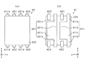
- FIG. 1 is a plan view showing a semiconductor module according to the first embodiment.
- FIG. 2 is a plan view showing a state in which the resin mold is removed in the semiconductor module shown in FIG.
- FIG. 3 is a cross-sectional view taken along the line III-III of FIG.
- FIG. 4 is a sectional view taken along line IV-IV of FIG.
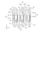
- FIG. 5 is a diagram in which a plurality of semiconductor modules shown in FIG. 1 are arranged side by side.
- FIG. 6 is a cross-sectional view showing the element structure of the semiconductor element in the semiconductor module shown in FIG. FIG.
- FIG. 7 is a schematic view of an electric power steering system to which the semiconductor module according to the first embodiment is applied.
- FIG. 8 is a diagram showing a drive circuit of an electric power steering system to which the semiconductor module shown in FIG. 1 can be applied.
- FIG. 9 is a plan view showing a semiconductor module according to a modified example.
- FIG. 10 is a plan view showing a semiconductor module according to a modified example.
- FIG. 11 is a plan view showing a semiconductor module according to a modified example.
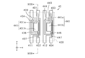
- FIG. 12 is a plan view showing the semiconductor module according to the second embodiment.
- FIG. 13 is a plan view showing a state in which the resin mold is removed in the semiconductor module shown in FIG.
- FIG. 14 is a sectional view taken along line XIV-XIV of FIG. FIG.
- FIG. 15 is a cross-sectional view taken along the line XV-XV of FIG.
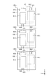
- FIG. 16 is a diagram in which a plurality of semiconductor modules shown in FIG. 12 are arranged side by side.
- FIG. 17 is a plan view showing a semiconductor module according to a modified example.
- FIG. 18 is a plan view showing a semiconductor module according to a modified example.
- FIG. 19 is a plan view showing a semiconductor module according to a modified example.
- FIG. 20 is a plan view showing the semiconductor module according to the third embodiment.
- FIG. 21 is a plan view showing a state in which the resin mold is removed in the semiconductor module shown in FIG.
- FIG. 22 is a sectional view taken along line XXII-XXII of FIG. FIG.
- FIG. 23 is a sectional view taken along line XXIII-XXIII of FIG.
- FIG. 24 is a diagram in which a plurality of semiconductor modules shown in FIG. 20 are arranged side by side.
- FIG. 25 is a plan view showing a semiconductor module according to a modified example.
- FIG. 26 is a plan view showing a semiconductor module according to a modified example.
- FIG. 27 is a plan view showing a semiconductor module according to a modified example.
- FIG. 28 is a plan view showing the semiconductor module according to the fourth embodiment.
- FIG. 29 is a plan view showing a state in which the resin mold is removed in the semiconductor module shown in FIG. 28.
- FIG. 30 is a sectional view taken along line XXII-XXII of FIG. 28.
- FIG. 31 is a diagram in which a plurality of semiconductor modules shown in FIG. 28 are arranged side by side.
- FIG. 32 is a plan view showing the semiconductor module according to the fifth embodiment.
- FIG. 33 is a plan view showing a state in which the resin mold is removed in the semiconductor module shown in FIG. 32.
- FIG. 34 is a diagram in which a plurality of semiconductor modules shown in FIG. 32 are arranged side by side.
- FIG. 35 is a diagram showing a drive circuit of an electric power steering system to which the semiconductor module shown in FIG. 32 can be applied.
- FIG. 36 is a plan view showing the semiconductor module according to the sixth embodiment.
- FIG. 37 is a plan view showing a state in which the resin mold is removed in the semiconductor module shown in FIG. 36.
- FIG. 38 is a sectional view taken along line XXXVIII-XXXVIII of FIG.
- FIG. 39 is a cross-sectional view taken along the line XXXIV-XXXIV of FIG.
- FIG. 40 is a diagram in which a plurality of semiconductor modules shown in FIG. 36 are arranged side by side.
- FIG. 41 is a diagram in which a set of semiconductor modules shown in FIG. 40 and another set of semiconductor modules are installed so as to be line-symmetrical on a wiring board.
- FIG. 42 is a diagram in which one set of semiconductor modules shown in FIG. 40 and another set of semiconductor modules are installed so as to be point-symmetrical on the wiring board.
- FIG. 43 is a diagram in which a plurality of semiconductor modules shown in FIG. 36 are arranged side by side.
- FIG. 44 is a diagram in which a plurality of semiconductor modules shown in FIG. 36 are arranged side by side.
- FIG. 45 is a diagram showing a mounting example of the semiconductor module according to the sixth embodiment.
- FIG. 46 is a diagram showing a mounting example of the semiconductor module according to the sixth embodiment.
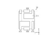
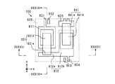
- the first semiconductor element 133 and the second semiconductor element 143 and the first semiconductor element 133 and the second semiconductor element 143 are integrally sealed. It includes a resin mold 120, conductive members 101 to 104, and conductive members 111, 112, 131, 141.
- the x-direction and the y-direction shown in FIGS. 1 to 5 are lateral to the semiconductor module 10, and the xy plane direction is the plane direction of the semiconductor module 10.
- the z direction is a vertical direction orthogonal to the plane direction.
- the semiconductor module 10 has four external terminals protruding in the negative direction of the y-axis from the resin mold 120 having a substantially rectangular shape when viewed from above, and is in the positive direction of the y-axis.
- the two external terminals have a protruding appearance.
- the four external terminals are a part of the conductive members 101 to 104 exposed from the resin mold 120, and the two external terminals are a part of the conductive members 111 and 112 exposed from the resin mold 120.
- the conductive member 112 includes a low-stage portion 112a that is not exposed from the resin mold 120 and a high-stage portion 112b that is exposed from the resin mold 120.
- the resin mold 120 is composed of a high heat dissipation resin material in which a resin material such as epoxy resin is mixed with a filler or the like for improving heat dissipation.
- a resin material such as epoxy resin
- a filler or the like for improving heat dissipation.
- a composite oxide material having high thermal conductivity such as alumina is selected.
- the thermal conductivity of the resin mold 120 can be adjusted by adjusting the type of filler and the filling rate.
- FIGS. 2 to 4 illustrate each configuration in the resin mold 120 of the semiconductor module 10.
- the positions where the resin mold 120 is provided are shown by broken lines.
- the first semiconductor element 133 and the second semiconductor element 143 are integrally sealed in a state of being arranged side by side in the x direction in the same direction. ..
- the first semiconductor element 133 and the second semiconductor element 143 are semiconductor elements having the same structure, shape, size, and the like, and are substantially rectangular when viewed from above.
- the gate pad 136 of the first semiconductor element 133 and the gate pad 146 of the second semiconductor element 143 are provided at the same position in each semiconductor element.
- the first semiconductor element 133 and the second semiconductor element 143 are arranged substantially parallel to each other in the same direction as the adjacent semiconductor element and to the adjacent semiconductor element.
- the first semiconductor element 133 and the second semiconductor element 143 are vertical insulated gate semiconductor elements having an element structure as shown in FIG. More specifically, it is a power MOSFET (Metal-Oxide-Semiconductor Field-Effective Transistor: MOSFET).
- MOSFET Metal-Oxide-Semiconductor Field-Effective Transistor: MOSFET
- the first semiconductor element 133 and the second semiconductor element 143 include a semiconductor substrate 60, a source electrode 71, and a drain electrode 72.
- the source electrode 71 is formed in contact with the upper surface 60u of the semiconductor substrate 60.
- the drain electrode 72 is formed in contact with the lower surface 60b of the semiconductor substrate 60.
- the upper surface 60u corresponds to the first surface
- the lower surface 60b corresponds to the second surface.
- the n + region 61, the n ⁇ region 62, and the p + region 63 are laminated on the semiconductor substrate 60 in this order from the lower surface 60b side.
- An n + region 64 is formed on a part of the upper surface side of the p + region 63.
- a trench 73 is formed from the upper surface 60u of the semiconductor substrate 60, penetrating the n + region 64 and the p + region 63, and reaching the upper surface side of the n ⁇ region 62.
- a gate insulating film 74 is formed on the inner wall surface of the trench 73, and the trench 73 is filled with the gate electrode 75 in a state of being insulated from the semiconductor substrate 60 by the gate insulating film 74.
- the upper surface of the gate electrode 75 is covered with an insulating film 76, and the gate electrode 75 and the source electrode 71 are insulated by the insulating film 76.
- the material of the semiconductor substrate 60 is not particularly limited, and examples thereof include silicon (Si), silicon carbide (SiC), and gallium nitride (GaN).
- the source electrode 71 corresponds to the first electrode, and among the external terminals, the source terminal electrically connected to the source electrode 71 corresponds to the first terminal.
- the drain electrode 72 corresponds to the second electrode, and among the external terminals, the drain terminal electrically connected to the drain electrode 72 corresponds to the second terminal.
- the first semiconductor element 133 and the second semiconductor element 143 are viewed from above with the source electrode 71 facing upward (positive direction of the z-axis) and the drain electrode facing downward (negative direction of the z-axis), respectively.
- the case is arranged so that the longitudinal direction is the y direction.
- the conductive member 131 includes a beam-shaped portion 131a, a pad portion 131b, and a columnar portion 131c.
- the pad portion 131b is located on the upper surface side of the first semiconductor element 133, and is a substantially rectangular portion having a size of the upper surface similar to that of the first semiconductor element 133.
- the beam-shaped portion 131a extends in the negative direction of the y-axis along the long side of the upper surface of the substantially rectangular shape of the pad portion 131b, and extends above the conductive member 102.
- the columnar portion 131c extends downward from the beam-shaped portion 131a, and its lower end surface is joined to the upper surface of the conductive member 102 via the joining member 135.
- the conductive member 101 is electrically connected to the gate pad 136 by the gate wiring 137.
- the conductive member 141 includes a beam-shaped portion 141a, a pad portion 141b, and a columnar portion 141c.
- the pad portion 141b is located on the upper surface side of the second semiconductor element 143, and is a substantially rectangular portion having a size of the upper surface similar to that of the second semiconductor element 143.
- the beam-shaped portion 141a extends in the negative direction of the y-axis along the long side of the upper surface of the substantially rectangular shape of the pad portion 141b, and extends above the conductive member 104.
- the columnar portion 141c extends downward from the beam-shaped portion 141a, and its lower end surface is joined to the upper surface of the conductive member 104 via the joining member 145.
- the conductive member 103 is electrically connected to the gate pad 146 by the gate wiring 147.
- the gate wirings 137 and 147 are so-called clips, but wire bonding, wire ribbons, and the like may be used in addition to the clips.
- the conductive members 101 and 102 correspond to the gate terminal and the source terminal of the first semiconductor element 133, and the conductive member 111 corresponds to the drain pad of the first semiconductor element 133.
- the conductive members 103 and 104 correspond to the gate terminal and the source terminal of the second semiconductor element 143, and the conductive member 112 corresponds to the drain pad of the second semiconductor element 143.
- the high step portion 112b of the conductive member 112 is exposed from the resin mold 120, while the low step portion 112a is not exposed from the resin mold 120. Therefore, when the semiconductor module 10 is viewed from the bottom, the portion exposed from the resin mold 120 of the drain pad (conductive member 112) of the second semiconductor element 143 is the resin mold 120 of the drain pad (conductive member 111) of the first semiconductor element 133. The area is smaller than the part exposed from. Between the exposed high step portion 112b and the conductive members 103 and 104, there is a region where nothing is exposed on the surface of the resin mold 120 because the low step portion 112a is covered with the resin mold 120. This area corresponds to the common wiring area.
- the lower portion 112a and the lower of the conductive members 111 are located between the long sides facing in the x direction. There is a region including a portion adjacent to the step portion 112a. Therefore, as shown in FIG. 5, when the three semiconductor modules 10 are arranged side by side in the same direction in the x direction so as to be substantially orthogonal to the long side facing the x direction, the region A1 that travels straight in a strip shape along the x direction. Can be secured.
- reference numbers of 10a, 10b, and 10c are assigned in order from the positive direction side of the x-axis at the arrangement position.
- the region A1c shown in FIG. 5 indicates the common wiring region A1c of the semiconductor module 10c.
- the common wiring region A1c is a strip-shaped region that travels substantially straight from one opposite side to the other on the surface of the resin mold 120 on which the conductive member 111 is exposed.
- the conductive member 111 exists in the common wiring region A1c, and no conductive member (conductive member 112 or the like) other than the conductive member 111 exists.
- the semiconductor modules 10a and 10b also have the same common wiring area as the common wiring area A1c.
- the width of the common wiring area A1c in the direction orthogonal to the wiring direction (x direction) is such that the wiring can be installed. For example, the installation intervals of the conductive members 101 to 104 (intervals in the x direction). ) Wider.
- Region A1 is included in a region connecting the common wiring region of the semiconductor modules 10a to 10c and the region between them. This region A1 extends over three semiconductor modules 10a, 10b, and 10c, and in the region A1, only the conductive member 111 is exposed from the resin mold 120. Therefore, by installing common wiring for connecting to the three conductive members 111 included in the three semiconductor modules 10a, 10b, and 10c in the region A1, the three conductive members 111 are electrically connected to each other. Can be done.
- the wiring width of the common wiring (width in the y direction orthogonal to the x direction, which is the wiring direction) is wider than the wiring width (width in the x direction) of the conductive members 101 to 104, and the width of the region A1 in the y direction is , The width that can install common wiring is secured.
- the conductive members 101 to 104, 111, 112 are exposed from the resin mold 120 on the upper surface side or the lower surface side of the semiconductor module 10.
- the conductive member 111 corresponds to the common wiring electrode
- the conductive members 101 to 104, 112 correspond to the non-common wiring electrode.
- the common wiring electrode is exposed from the resin mold 120 on the upper surface side (positive direction side of the z-axis) or the lower surface side (negative direction side of the z-axis) of the semiconductor module 10, and is the first electrode (source electrode 71) and the first electrode. It is an electrode that is electrically connected to at least one of the two electrodes (drain electrode 72).
- the common wiring electrode is connected to the common wiring when the semiconductor module 10 is connected to another semiconductor module by the common wiring.
- common wiring can be installed from one side facing the x-axis direction to the other side.
- the semiconductor module 10 when the common wiring is connected to the common wiring electrode (conductive member 111), the common wiring is not electrically connected to the non-common wiring electrode (conductive members 101 to 104, 112).
- Each configuration (plurality of semiconductor elements, a plurality of conductive members, etc.) constituting the semiconductor module 10 allows common wiring to be installed from one opposite side to the other side on the surface of the resin mold on which the electrodes are exposed. Have been placed. Therefore, the plurality of semiconductor modules 10 can be electrically connected to each other on the lower surface side of the semiconductor module 10. As a result, the wiring space on the side of the semiconductor module 10 can be reduced, which can contribute to the miniaturization of the mounting board.
- the resin mold 120 is made of a high heat dissipation resin material, heat dissipation of the semiconductor module 10 can be promoted via the resin mold 120.
- the semiconductor module 10 can be applied to the drive circuit of the electric power steering system (EPS) 80 of the vehicle as shown in FIG.
- the EPS 80 includes a steering wheel 90, a steering shaft 91, a pinion gear 92, a rack shaft 93, and an EPS device 81 that form a steering wheel.
- a steering shaft 91 is connected to the steering wheel 90.
- a pinion gear 92 is provided at the tip of the steering shaft 91.
- the pinion gear 92 meshes with the rack shaft 93.
- Wheels 95 are rotatably connected to both ends of the rack shaft 93 via a tie rod or the like.
- the EPS device 81 includes a torque sensor 94, a speed reducer 96, a rotary electric machine 82, and an energization circuit unit 83.
- the torque sensor 94 is provided on the steering shaft 91 and detects the steering torque Trq, which is the output torque of the steering shaft 91.
- the rotary electric machine 82 generates an auxiliary torque according to the detected steering torque Trq and the steering direction of the steering wheel 90.
- the energizing circuit unit 83 controls the drive of the rotary electric machine 82.
- the speed reducer 96 transmits auxiliary torque to the steering shaft 91 while decelerating the rotation of the rotation shaft of the rotor of the rotary electric machine 82.
- the stator of the rotary electric machine 82 includes a first winding group M1 and a second winding group M2.
- the first winding group M1 includes a star-shaped first U-phase winding U1, a first V-phase winding V1, and a first W-phase winding W1, and the second winding group M2 has a star-shaped connection. It includes a 2U phase winding U2, a second V phase winding V2, and a second W phase winding W2.
- the first ends of the first U, V, W phase windings U1, V1, W1 are connected at a neutral point.
- the first U, V, W phase windings U1, V1, W1 are deviated by 120 ° at the electric angle ⁇ e.
- the first ends of the second U, V, W phase windings U2, V2, W2 are connected at a neutral point.
- the second U, V, and W phase windings U2, V2, and W2 are deviated by 120 ° at the electric angle ⁇ e.
- the energization circuit unit 83 includes a first inverter INV1 and a second inverter INV2 as power converters, and a first relay RL1 and a second relay RL2 as power relays.
- the second end of the first U phase winding U1 is connected to the connection point between the upper arm switch SU1p and the lower arm switch SU1n of the first U phase.
- the second end of the first V phase winding V1 is connected to the connection point between the upper arm switch SV1p of the first V phase and the lower arm switch SV1n.
- the second end of the first W phase winding W1 is connected to the connection point between the upper arm switch SW1p of the first W phase and the lower arm switch SW1n.
- the second end of the second U-phase winding U2 is connected to the connection point between the upper arm switch SU2p and the lower arm switch SU2n of the second U phase.
- the second end of the second V-phase winding V2 is connected to the connection point between the upper arm switch SV2p and the lower arm switch SV2n of the second V phase.
- the second end of the second W phase winding W2 is connected to the connection point between the upper arm switch SW2p and the lower arm switch SW2n of the second W phase.
- the high potential side terminals of the upper arm switches SU1p, SV1p, SW1p of the first U, V, W phases are connected to the positive electrode terminal of the battery 97, which is a DC power supply, via the first relay RL1.
- the low potential side terminals of the lower arm switches SU1n, SV1n, SW1n of the first U, V, W phase are connected to the ground via the resistors RU1, RV1, RW1.
- the high potential side terminals of the upper arm switches SU2p, SV2p, SW2p of the second U, V, W phase are connected to the positive electrode terminal of the battery 97 via the second relay RL2.
- the low potential side terminals of the lower arm switches SU2n, SV2n, SW2n of the second U, V, W phase are connected to the ground via the resistors RU2, RV2, RW2.
- the negative electrode terminal of the battery 97 is connected to the ground.
- MOSFETs as exemplified in the first semiconductor element 133 and the second semiconductor element 143 can be used.
- Two switches SU1p and SU1n, SV1p and SV1n, SW1p and SW1n, SU2p and SU2n, SV2p and SV2n, SW2p and SW2n, which are connected in series in each arm, are the source electrode of the former MOSFET and the drain of the latter MOSFET, respectively.
- the electrodes are connected and connected in series.
- Semiconductor modules SU1, SV1, SW1, SU2 that integrate two switches SU1p and SU1n, SV1p and SV1n, SW1p and SW1n, SU2p and SU2n, SV2p and SV2n, and SW2p and SW2n connected in series in each arm.
- the semiconductor module 10 can be used as the SV2 and SW2.
- the semiconductor module 10 can be applied to the first inverter INV1 and the second inverter INV2 to form an inverter circuit.
- MOSFETs as exemplified in the first semiconductor element 133 and the second semiconductor element 143 can be used.
- the switches SP1 and SP2 are power relay switches, and the switches SC1 and SC2 are reverse connection protection relays.
- the two switches SP1 and SC1, SP2 and SC2, which are connected in series in each arm, are connected in series by connecting the source electrodes of the MOSFETs to each other.
- the energization circuit unit 83 detects the current flowing through the resistors RU1, RV1, RW1 and outputs the currents as the first U, V, W phase currents Iur1, Ivr1, Iwr1. Further, the current flowing through the RU2, RV2, and RW2 is detected and output as the second U, V, and W phase currents Iur2, Ivr2, and Iwr2.
- the energization circuit unit 83 includes an ECU mainly composed of a microcomputer, and the ECU operates each switch of the first inverter INV1 and the second inverter INV2 in order to control the torque of the rotary electric machine 82 to the torque command value Tr *. To do.
- the torque command value Tr * is set based on, for example, the steering torque Trq detected by the torque sensor 94.
- the energization circuit unit 83 calculates the electric angle ⁇ e of the rotary electric machine 82 based on the output signal of the angle sensor by the ECU.
- an angle sensor for example, an angle sensor including a magnet which is a magnet generating portion provided on the rotor side of the rotary electric machine 82 and a magnetic detection element provided close to the magnet can be exemplified. ..
- the functions provided by the above-mentioned ECU can be provided, for example, by software recorded in a substantive memory device and a computer, hardware, or a combination thereof that executes the software.
- the semiconductor module 10 can be applied to the EPS 80, and can be applied to the energization circuit unit 83 corresponding to the drive circuit of the EPS 80 as the semiconductor modules SU1 to SW2 including two switches connected in series. it can.
- the semiconductor module 10 can be applied to the inverter circuits shown as the first inverter INV1 and the second inverter INV2, respectively, and the first semiconductor element 133 and the second semiconductor element 143 are connected in series, respectively. It is applied to inverter circuits as a switching element.
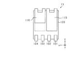
- the semiconductor module 10 As shown in FIG. 1A, as the semiconductor module 10, the conductive members 131 and 141 have been described by way of example when they are not exposed from the resin mold 120, but the present invention is not limited to this. Like the semiconductor module 11 shown in FIG. 9, the semiconductor module 11 may be provided with conductive members 151 and 161 protruding from the resin mold 120 on the upper surface side thereof. Since the other configurations of the semiconductor module 11 are the same as those of the semiconductor module 10, the description thereof will be omitted.
- the conductive members 111 and 112 extend beyond the positive direction of the y-axis of the resin mold 120 by way of example, but the present invention is not limited to this.
- the resin mold 120 may include conductive members 113 and 114 that do not exceed the positive direction of the y-axis. Since the other configurations of the semiconductor module 12 are the same as those of the semiconductor module 10, the description thereof will be omitted.
- the resin mold 120 may include conductive members 115 and 116 in which a portion extending beyond the positive direction of the y-axis is branched into two. .. Since the other configurations of the semiconductor module 13 are the same as those of the semiconductor module 10, the description thereof will be omitted.
- first semiconductor element 133 first semiconductor element 133, second semiconductor element 143
- the semiconductor elements may be arranged substantially point-symmetrically with the adjacent semiconductor elements in the opposite direction to the adjacent semiconductor elements.
- the second semiconductor element 243 has a vertical direction (z direction) with respect to the first semiconductor element 233. It is integrally sealed in a state where it is arranged side by side in the x-axis direction in a direction rotated by 180 ° to the center. That is, the first semiconductor element 233 and the second semiconductor element 243 are arranged substantially point-symmetrically with the adjacent semiconductor elements in the opposite directions to the adjacent semiconductor elements.
- the first semiconductor element 233 and the second semiconductor element 243 are semiconductor elements having the same structure, shape, size, and the like. The material, shape, size, and the like of each configuration included in the semiconductor module 20 are the same as those of each configuration included in the semiconductor module.
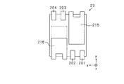
- each configuration on the first semiconductor element 233 side that is, the conductive member 231 and the joining member 232, the first semiconductor element 233, the joining member 234, and the conductive member 211 are the first in the first embodiment. 1 Since the semiconductor elements are arranged in the same manner as each configuration on the 133 side, the description will be omitted by replacing the reference number in the 100s with the 200s.
- the conductive member 241 and the joining member 242, the second semiconductor element 243, the joining member 244, and the conductive member 212 are upward as in the first embodiment. It is arranged in this order from.
- the conductive member 241 includes a beam-shaped portion 241a, a pad portion 241b, and a columnar portion 241c.
- the beam-shaped portion 241a extends in the positive direction of the y-axis along the long side of the upper surface of the substantially rectangular shape of the pad portion 241b, and extends above the conductive member 203.
- the columnar portion 241c extends downward from the beam-shaped portion 241a, and its lower end surface is joined to the upper surface of the conductive member 203 via the joining member 245.
- the conductive member 204 is electrically connected to the gate pad 246 by the gate wiring 247.
- the conductive members 201 and 202 correspond to the gate terminal and the source terminal of the first semiconductor element 233, and the conductive member 211 corresponds to the drain pad of the first semiconductor element 233.
- the conductive members 203 and 204 correspond to the source terminal and the gate terminal of the second semiconductor element 243, and the conductive member 212 corresponds to the drain pad of the second semiconductor element 243.
- the high step portion 212b of the conductive member 212 is exposed from the resin mold 220, while the low step portion 212a is not exposed from the resin mold 220. Therefore, when the semiconductor module 20 is viewed from the bottom, the portion exposed from the resin mold 220 of the drain pad (conductive member 212) of the second semiconductor element 243 is the resin mold 220 of the drain pad (conductive member 211) of the first semiconductor element 233. The area is smaller than the part exposed from. Between the exposed high step portion 212b and the conductive members 203 and 204, there is a region where nothing is exposed on the surface of the resin mold 220 because the low step portion 212a is covered with the resin mold 220. This area corresponds to the common wiring area.
- the lower portion 212a and the lower of the conductive members 211 are located between the long sides facing in the x direction.
- a portion adjacent to the step portion 212a is included. Therefore, as shown in FIG. 16, when the three semiconductor modules 20 are arranged side by side in the same direction in the x direction so as to be substantially orthogonal to the long side facing the x direction, the region A2 that travels straight in a strip shape along the x direction. Can be secured.
- reference numbers of 20a, 20b, and 20c are assigned in order from the positive direction side of the x-axis at the arrangement position.
- the common wiring region A2c is a strip-shaped region that travels substantially straight from one opposite side to the other on the surface of the resin mold 220 on which the conductive member 211 is exposed.
- the conductive member 211 exists in the common wiring region A2c, and no conductive member other than the conductive member 211 exists.
- the semiconductor modules 20a and 20b also have the same common wiring area as the common wiring area A2c.
- Region A2 is included in a region connecting the common wiring region of the semiconductor modules 20a to 20c and the region between them. This region A2 extends over three semiconductor modules 20a, 20b, and 20c, and in the region A2, only the conductive member 211 is exposed from the resin mold 220. Therefore, by installing common wiring for connecting to the three conductive members 211 included in the three semiconductor modules 20a, 20b, and 20c in the region A2, the three conductive members 211 are electrically connected to each other. Can be done.
- the conductive members 201 to 204, 211,212 are exposed from the resin mold 220 on the upper surface side or the lower surface side of the semiconductor module 20.
- the conductive member 211 corresponds to the common wiring electrode
- the conductive members 201 to 204, 212 correspond to the non-common wiring electrode.
- the bottom surface of the resin mold 220 is in the x direction without being electrically connected to the electrodes for non-common wiring (conductive members 201 to 204, 212).
- Common wiring can be installed from one side facing the other side to the other side.
- the wiring width of the common wiring (width in the y direction orthogonal to the x direction, which is the wiring direction) is wider than the wiring width (width in the x direction) of the conductive members 201 to 204, and the width of the region A2 in the y direction is , The width that can install common wiring is secured.
- the common wiring electrode is exposed without being electrically connected to the non-common wiring electrode.
- Each configuration (a plurality of semiconductor elements, a plurality of conductive members, etc.) constituting the semiconductor module 20 is arranged so that the common wiring can be installed from one opposite side to the other side on the surface of the resin mold. .. Therefore, the plurality of semiconductor modules 20 can be electrically connected to each other on the lower surface side of the semiconductor module 20. As a result, the wiring space on the side of the semiconductor module 20 can be reduced, which can contribute to the miniaturization of the mounting board.
- the resin mold 220 is made of a high heat dissipation resin material, heat dissipation of the semiconductor module 20 can be promoted via the resin mold 220.
- the semiconductor module 20 can be applied to the EPS 80 in the same manner as the semiconductor module 10, and is a semiconductor module SU1 to SW2 including two switches connected in series, and is an energization circuit unit 83 corresponding to the drive circuit of the EPS 80. Can be applied to.
- the semiconductor modules 21 to 23 shown in FIGS. 17 to 19 can be applied as modification examples.
- the conductive members 251,261 protruding from the resin mold 220 may be provided instead of the conductive members 231,241.
- the conductive members 213 and 214 that do not exceed the positive direction of the y-axis of the resin mold 220 may be provided.
- the resin mold 220 may include conductive members 215 and 216 in which a portion extending beyond the positive direction of the y-axis is branched into two. .. Since the other configurations of the semiconductor modules 21 to 23 are the same as those of the semiconductor module 20, the description thereof will be omitted.
- the plurality of semiconductor elements are arranged side by side in the direction (y direction) in which the conductive member protrudes as an external terminal (x direction), but the external terminals are arranged. They may be arranged side by side in the protruding direction.
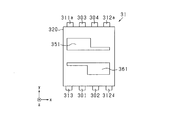
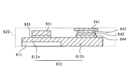
- the second semiconductor element 343 has a vertical direction (z direction) with respect to the first semiconductor element 333. It is integrally sealed in a state where it is arranged side by side in the y direction in a direction rotated by 180 ° to the center. That is, the first semiconductor element 333 and the second semiconductor element 343 are arranged substantially point-symmetrically with the adjacent semiconductor elements in the opposite directions to the adjacent semiconductor elements. As in the first embodiment, the first semiconductor element 333 and the second semiconductor element 343 are semiconductor elements having the same structure, shape, size, and the like. The first semiconductor element 333 and the second semiconductor element 343 are arranged so that the longitudinal direction when viewed from above is parallel to the x-axis.
- the conductive member 331 includes a beam-shaped portion 331a, a pad portion 331b, and a columnar portion 331c.
- the beam-shaped portion 331a extends in the positive direction of the x-axis along the long side of the upper surface of the substantially rectangular shape of the pad portion 331b, and extends above the conductive member 312.
- the columnar portion 331c extends downward from the beam-shaped portion 331a, and its lower end surface is joined to the upper surface of the conductive member 312 via a joining member (not shown).
- the conductive member 304 is electrically connected to the gate pad 346 by the gate wiring 347.
- the conductive member 341 includes a beam-shaped portion 341a, a pad portion 341b, and a columnar portion 341c.
- the beam-shaped portion 341a extends in the negative direction of the x-axis along the long side of the upper surface of the substantially rectangular shape of the pad portion 341b, and extends above the conductive member 313.
- the columnar portion 341c extends downward from the beam-shaped portion 341a, and its lower end surface is joined to the upper surface of the conductive member 313 via a joining member (not shown).
- the conductive member 301 is electrically connected to the gate pad 346 by the gate wiring 347.
- the conductive member 311 has a substantially L-shape, and includes a terminal portion 311a and an element installation portion 311b.
- the first semiconductor element 333 is installed in the element installation portion 311b.
- the terminal portion 311a extends from the element installation portion 311b in the positive direction of the y-axis and extends beyond the end portion of the resin mold 320 on the positive direction side of the y-axis.
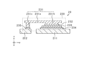
- the conductive member 312 includes a first terminal portion 312a, a lower stage portion 312b, an element installation portion 312c, and a second terminal portion 312d.
- the second semiconductor element 343 is installed in the element installation unit 312c.
- the lower step portion 312b and the first terminal portion 312a are elongated strip-shaped and substantially rectangular portions extending from the end portion of the element installation portion 312c on the positive direction side of the x-axis to the positive direction side of the y-axis, and the lower stage portion 312b. Is closer to the element installation portion 312c.
- the second terminal portion 312d is a strip-shaped and substantially rectangular portion extending from the end portion of the element installation portion 312c on the positive direction side of the x-axis to the negative direction side of the y-axis.
- the conductive member 312 is in contact with the drain electrode of the second semiconductor element 343 via the joining member 344 in the element installation portion 312c and is electrically connected. Further, the conductive member 312 is electrically connected to the source electrode of the first semiconductor element 333 at the lower stage portion 312b via the conductive member 331, the joining member 332, and the like. That is, the conductive member 312 joins the first electrode (source electrode) of the first semiconductor element 333 and the second electrode (drain electrode) of the second semiconductor element 343 arranged adjacent to the first semiconductor element 333. Corresponds to the joint conductive member to be formed.
- the conductive member 313 has an elongated strip shape and a substantially rectangular shape, from the end portion of the element installation portion 312c of the conductive member 312 on the positive direction side of the y-axis to beyond the end portion of the resin mold 320 on the negative direction side of the y-axis. It is postponed.
- the conductive members 304 and 312 correspond to the gate terminal and the source terminal of the first semiconductor element 333, and the conductive member 311 corresponds to the drain pad of the first semiconductor element 333.
- the conductive members 301 and 313 correspond to the gate terminal and the source terminal of the second semiconductor element 343, and the conductive member 312 corresponds to the drain pad of the second semiconductor element 343.
- the first terminal portion 312a, the element installation portion 312c, and the second terminal portion 312d of the conductive member 312 correspond to the high-stage portion and are exposed from the resin mold 320 while being exposed.
- the lower step 312b is not exposed from the resin mold 320. Therefore, when the semiconductor module 30 is viewed from the bottom, it seems that the first terminal portion 312a and the element mounting portion 312c are not connected, while the second terminal portion 312d and the element mounting portion 312c are connected.
- the lower step portion 312b is adjacent to a part of the element installation portion 311b of the conductive member 311 in the x direction.
- the lower step portion 312b is covered with the resin mold 320 between the exposed first terminal portion 312a and the element installation portion 312c, so that nothing is exposed on the surface of the resin mold 320.
- the lower step portion 312b and the element of the conductive member 311 are installed between the long sides facing in the x direction.
- a portion of the portion 311b adjacent to the lower portion 312b is included. Therefore, as shown in FIG. 24, when the three semiconductor modules 30 are arranged side by side in the same direction in the x direction so as to be substantially orthogonal to the long side facing the x direction, the region A3 that goes straight in a band shape along the x direction. Can be secured.
- reference numbers of 30a, 30b, and 30c are assigned in order from the positive direction side of the x-axis at the arrangement position.
- the region A3c shown in FIG. 24 indicates the common wiring region A3c of the semiconductor module 30c.
- the common wiring region A3c is a strip-shaped region that travels substantially straight from one opposite side to the other on the surface of the resin mold 320 on which the conductive member 311 is exposed.
- the conductive member 311 exists in the common wiring region A3c, and no conductive member other than the conductive member 311 exists.
- the semiconductor modules 30a and 30b also have the same common wiring area as the common wiring area A3c.
- Region A3 is included in the region connecting the common wiring region of the semiconductor modules 30a to 30c and the region between them. This region A3 extends over three semiconductor modules 30a, 30b, and 30c, and in the region A3, only the conductive member 311 (more specifically, the element mounting portion 311b) is exposed from the resin mold 320. Therefore, by installing common wiring for connecting to the three conductive members 311 included in the three semiconductor modules 30a, 30b, and 30c in the region A3, the three conductive members 311 are electrically connected to each other. Can be done.
- the conductive members 301 to 304 and 311 to 313 are exposed from the resin mold 320 on the upper surface side or the lower surface side of the semiconductor module 30.
- the conductive member 311 corresponds to the common wiring electrode
- the conductive members 301 to 304, 312, 313 correspond to the non-common wiring electrode.
- each configuration (a plurality of semiconductor elements, a plurality of conductive members, etc.) constituting the semiconductor module 30 is arranged so that the common wiring can be installed from one opposite side to the other side on the surface of the resin mold. ing. Therefore, the plurality of semiconductor modules 30 can be electrically connected to each other on the lower surface side of the semiconductor module 30. As a result, the wiring space on the side of the semiconductor module 30 can be reduced, which can contribute to the miniaturization of the mounting board.
- the resin mold 320 is made of a high heat dissipation resin material, heat dissipation of the semiconductor module 30 can be promoted via the resin mold 320.
- the semiconductor module 30 can be applied to the EPS 80 in the same manner as the semiconductor module 10, and is a semiconductor module SU1 to SW2 including two switches connected in series, and is an energization circuit unit 83 corresponding to the drive circuit of the EPS 80. Can be applied to.
- the semiconductor modules 31 to 33 shown in FIGS. 25 to 27 can be applied as a modification.
- the conductive members 351 and 361 protruding from the resin mold 320 may be provided on the upper surface side thereof instead of the conductive members 331 and 341.
- a conductive member 305 in which these are integrated may be provided.
- a conductive member 306 that integrates these members may be provided.
- the conductive member 305 is a gate terminal of the first semiconductor element 333
- the conductive member 306 is a gate terminal of the second semiconductor element 343.
- one of the conductive members 301 and 302 may not be provided.
- one of the conductive members 303 and 304 may not be provided.
- the semiconductor module 33 is not provided with the conductive members 301 and 303. On the contrary, since the other configurations of the semiconductor modules 31 to 33 are the same as those of the semiconductor module 30, the description thereof will be omitted.
- the conductive member 112 corresponding to the non-common wiring electrode includes a high step portion 112b that is higher toward the lower surface side exposed from the resin mold 120 and a lower step portion 112a that is lower than the high step portion 112b. This allows common wiring, but is not limited to this.
- the first semiconductor element 433 and the second semiconductor element 443 are arranged side by side in the x direction in the same direction in the resin mold 420. It is integrally sealed in the closed state. That is, the first semiconductor element 433 and the second semiconductor element 443 are arranged substantially parallel to each other in the same direction as the adjacent semiconductor element and to the adjacent semiconductor element. As in the first embodiment, the first semiconductor element 433 and the second semiconductor element 443 are semiconductor elements having the same structure, shape, size, and the like. The first semiconductor element 433 and the second semiconductor element 443 are arranged so that the longitudinal direction when viewed from above is parallel to the x-axis.
- the conductive member 431, the joining member 432, the first semiconductor element 433, the joining member 434, and the conductive member 411 are located above, as in the first embodiment. It is arranged in this order from.
- the conductive member 431 includes a beam-shaped portion 431a, a pad portion 431b, and a columnar portion 431c.
- the beam-shaped portion 431a extends in the positive direction of the y-axis along the long side of the upper surface of the substantially rectangular shape of the pad portion 431b, and extends above the conductive member 412.
- the columnar portion 431c extends downward from the beam-shaped portion 431a, and its lower end surface is joined to the upper surface of the conductive member 401 via a joining member (not shown).
- the conductive member 402 is electrically connected to the gate pad 446 by the gate wiring 447.
- the conductive member 441 includes a beam-shaped portion 441a, a pad portion 441b, and a columnar portion 441c.
- the beam-shaped portion 441a extends in the positive direction of the y-axis along the long side of the upper surface of the substantially rectangular shape of the pad portion 441b, and extends above the conductive member 403.
- the columnar portion 441c extends downward from the beam-shaped portion 441a, and its lower end surface is joined to the upper surface of the conductive member 403 via a joining member (not shown).
- the conductive member 404 is electrically connected to the gate pad 446 by the gate wiring 447.
- Each configuration on the second semiconductor element 443 side is a state in which each configuration on the first semiconductor element 433 side is moved in the positive direction of the x-axis, and each configuration has the same shape, size, and positional relationship. There is.
- the conductive members 401 and 402 correspond to the source terminal and the gate terminal of the first semiconductor element 433, and the conductive member 411 corresponds to the drain pad of the first semiconductor element 433.
- the conductive members 403 and 404 correspond to the source terminal and the gate terminal of the second semiconductor element 243, and the conductive member 412 corresponds to the drain pad of the second semiconductor element 443.
- the conductive member 411 has a substantially T-shape, and includes a first terminal portion 411a, an element installation portion 411b, an intermediate portion 411c, and a second terminal portion 411d.
- the element installation portion 411b is provided substantially in the center of the conductive member 411 in the y direction, and the intermediate portion 411c is located on the negative direction side of the x-axis with respect to the element installation portion 411b.
- the first terminal portion 411a is provided on the positive direction side of the y-axis and extends beyond the end portion of the resin mold 420 on the positive direction side of the y-axis.
- the second terminal portion 411d is provided on the negative direction side of the y-axis and extends beyond the end portion of the resin mold 420 on the negative direction side of the y-axis.
- the intermediate portion 411c is a portion between the first terminal portion 411a and the second terminal portion 411d.
- the first semiconductor element 433 is installed in the element installation portion 411b. Since the shape of the conductive member 412 is the same as that of the conductive member 411, the description will be omitted by replacing 411 in the reference number with 412.
- the common wiring region A4c is a strip-shaped region that travels substantially straight from one opposite side to the other on the surface of the resin mold 420 on which the conductive member 411 is exposed.
- the conductive member 411 exists in the common wiring region A4c, and no conductive member other than the conductive member 411 exists.
- the semiconductor modules 40a and 40b also have the same common wiring area as the common wiring area A4c.
- Region A4 is included in a region connecting the common wiring region of the semiconductor modules 40a to 40c and the region between them.
- This region A4 extends over three semiconductor modules 40a, 40b, and 40c, and in the region A4, only the conductive member 411 is exposed from the resin mold 420. Therefore, by installing common wiring for connecting to the three conductive members 411 included in the three semiconductor modules 40a, 40b, and 40c in the region A4, the three conductive members 411 are electrically connected to each other. Can be done.
- the conductive member 412 in the resin mold 420 which is substantially rectangular when the semiconductor module 40 is viewed from the bottom, the conductive member is between the short sides facing in the y direction. There is a region that contains only 412. Therefore, common wiring connected to the three conductive members 412 included in the three semiconductor modules 40a, 40b, and 40c can be installed.
- the conductive members 401 to 404, 411, 412 are exposed from the resin mold 420 on the upper surface side or the lower surface side of the semiconductor module 40.
- the conductive members 411 and 412 correspond to the electrodes for common wiring
- the conductive members 401 to 404 correspond to the electrodes for non-common wiring.
- Common wiring can be installed from one side facing the x direction to the other side.
- the wiring width of the common wiring (width in the x direction orthogonal to the y direction, which is the wiring direction) is wider than the wiring width (width in the x direction) of the conductive members 401 to 404, and the width of the region A4 in the x direction is , The width that can install common wiring is secured.
- the common wiring electrode is not electrically connected to the non-common wiring electrode.
- Each configuration (a plurality of semiconductor elements, a plurality of conductive members, etc.) constituting the semiconductor module 40 can be installed so that the common wiring can be installed from one opposite side to the other side on the surface of the resin mold to which is exposed. Have been placed. Therefore, the plurality of semiconductor modules 40 can be electrically connected to each other on the lower surface side of the semiconductor module 40. As a result, the wiring space on the side of the semiconductor module 40 can be reduced, which can contribute to the miniaturization of the mounting board.
- the resin mold 420 is made of a high heat dissipation resin material, heat dissipation of the semiconductor module 40 can be promoted via the resin mold 420.
- the electrodes for common wiring extend to positions protruding from both of the pair of opposite sides of the surface of the resin mold. With this configuration, common wiring can be realized without providing a step in the thickness direction of the conductive member. Further, in the semiconductor module 40, since it is not necessary to separately make the conductive member on the first semiconductor element side and the conductive member on the second semiconductor element side, the configuration is simple and it can contribute to reduction of manufacturing cost and the like.
- the first semiconductor element 533, the second semiconductor element 543, and the third semiconductor element 553 have the same orientation in the resin mold 520. It is integrally sealed in a state where it is arranged side by side in the x direction.
- the semiconductor module 50 has a configuration in which a third semiconductor element 553 and a conductive member loaded or connected to the third semiconductor element 553 are further added to the semiconductor module 40. Since each configuration on the first semiconductor element 533 side and each configuration on the second semiconductor element 543 side are the same as each configuration on the first semiconductor element 433 side and each configuration on the second semiconductor element 443 side in the semiconductor module 40, The description will be omitted by replacing the reference number in the 400 series with the reference number in the 500 series.
- Each configuration on the third semiconductor element 553 side is a state in which each configuration on the first semiconductor element 533 side or each configuration on the second semiconductor element 543 side is moved in the positive direction of the x-axis, and each configuration has the same shape. , Size, and positional relationship.
- the conductive member 581 includes a beam-shaped portion 581a, a pad portion 581b, and a columnar portion (not shown).
- the beam-shaped portion 581a extends in the positive direction of the y-axis along the long side of the upper surface of the substantially rectangular shape of the pad portion 581b, and extends above the conductive member 505.
- the columnar portion extends downward from the beam-shaped portion 581a, and its lower end surface is joined to the upper surface of the conductive member 505 via a joining member (not shown).
- the conductive member 506 is electrically connected to the gate pad by a gate wiring.
- the conductive members 501 and 502 correspond to the source terminal and the gate terminal of the first semiconductor element 533, and the conductive member 511 corresponds to the drain pad of the first semiconductor element 533.
- the conductive members 503 and 504 correspond to the source terminal and the gate terminal of the second semiconductor element 543, and the conductive member 512 corresponds to the drain pad of the second semiconductor element 543.
- the conductive members 505 and 506 correspond to the source terminal and the gate terminal of the third semiconductor element 553, and the conductive member 571 corresponds to the drain pad of the third semiconductor element 553.
- the region A5c shown in FIG. 34 indicates the common wiring region A5c of the semiconductor module 50c.
- the common wiring region A5c is a strip-shaped region that travels substantially straight from one opposite side to the other on the surface of the resin mold 520 on which the conductive member 511 is exposed.
- the conductive member 511 exists in the common wiring region A5c, and no conductive member other than the conductive member 511 exists.
- the semiconductor modules 50a and 50b also have the same common wiring area as the common wiring area A5c.
- Region A5 is included in the region connecting the common wiring region of the semiconductor modules 50a to 50c and the region between them. This region A5 extends over three semiconductor modules 50a, 50b, and 50c, and in the region A5, only the conductive member 511 is exposed from the resin mold 520. Therefore, by installing common wiring for connecting to the three conductive members 511 included in the three semiconductor modules 50a, 50b, and 50c in the region A5, the three conductive members 511 are electrically connected to each other. Can be done.
- the wiring width of the common wiring (width in the x direction orthogonal to the y direction, which is the wiring direction) is wider than the wiring width (width in the x direction) of the conductive members 501 to 506, and the width of the region A5 in the x direction is , The width that can install common wiring is secured.
- the semiconductor module according to this embodiment can be used in a drive circuit as shown in FIG. 35.
- the drive circuit shown in FIG. 35 corresponds to a drive circuit shown in FIG. 8 to which the motor relay switches TU1, TV1, TW1, TU2, TV2, and TW2 are added.
- the connection point between the upper arm switch SU1p and the lower arm switch SU1n of the first U phase and the second end of the first U phase winding U1 are connected via the motor relay switch TU1.
- the connection point between the upper arm switch SV1p and the lower arm switch SV1n of the first V phase and the second end of the first V phase winding V1 are connected via the motor relay switch TV1.
- connection point between the upper arm switch SW1p and the lower arm switch SW1n of the first W phase and the second end of the first W phase winding U1 are connected via the motor relay switch TW1.
- the connection point between the upper arm switch SU2p and the lower arm switch SU2n of the second U phase and the second end of the second U phase winding U2 are connected via the motor relay switch TU2.
- the connection point between the upper arm switch SV2p and the lower arm switch SV2n of the second V phase and the second end of the second V phase winding V2 are connected via the motor relay switch TV2.
- the connection point between the upper arm switch SW2p and the lower arm switch SW2n of the second W phase and the second end of the second W phase winding U2 are connected via the motor relay switch TW2.
- the semiconductor module 50 can be applied to the EPS 80, and is applied to the energization circuit unit 83 corresponding to the drive circuit of the EPS 80 as the semiconductor modules SU1 to SW2 including two switches connected in series and a motor relay switch. be able to. Further, it may be configured as a semiconductor module in which SU1, SV1 and SW1 shown in FIG. 8 are integrated.
- the semiconductor module including the low-stage portion 112a and the high-stage portion 112b in the conductive member 112 corresponding to the non-common wiring electrode described in the first embodiment also includes three or more semiconductor elements.
- Common wiring can be made possible.
- a semiconductor including three semiconductor elements capable of common wiring by adding each configuration on the second semiconductor element 143 side to the semiconductor module 10 on the positive direction side of the x-axis. Modules can be realized.
- the semiconductor module 160 integrally seals the first semiconductor element 633 and the second semiconductor element 643 and the first semiconductor element 633 and the second semiconductor element 643. It includes a resin mold 620, conductive members 601 to 605, and conductive members 611, 612, 631, 641.
- the x-direction and the y-direction shown in FIGS. 36 to 39 are the sides of the semiconductor module 160, and the xy plane direction is the plane direction of the semiconductor module 160.
- the z direction is a vertical direction orthogonal to the plane direction.
- FIG. 36 (a) is a top view of the semiconductor module 160
- FIG. 36 (b) is a bottom view of the semiconductor module 160
- FIG. 37 is a top view of each configuration in the resin mold 120 of the semiconductor module 160
- FIGS. 38 and 39 are cross-sectional views of each configuration in the resin mold 120 of the semiconductor module 160. In FIGS. 37 to 39, the positions where the resin mold 120 is provided are shown by broken lines.
- the second semiconductor element 643 is rotated by 180 ° about the vertical direction (z direction) with respect to the first semiconductor element 633 and the x-axis. They are integrally sealed while being arranged side by side in the direction.
- the first semiconductor element 633 and the second semiconductor element 643 are semiconductor elements having the same structure, shape, size, and the like, and are substantially rectangular when viewed from above.
- the conductive member 631, the joining member 632, the first semiconductor element 633, the joining member 634, and the conductive member 611 are arranged in this order from above.
- the conductive member 641, the bonding member 642, the second semiconductor element 643, the bonding member 644, and the conductive member 612 are arranged in this order from above.
- the entire lower surfaces of the conductive members 601 to 605 and the conductive members 111 are exposed from the resin mold 620.
- the conductive members 601 to 605 that function as gate terminals, source terminals, or drain terminals are located on the lower surface side (negative direction of the z-axis) of the resin mold 620. While exposed, it does not protrude laterally in the y direction.
- the conductive member 612 includes a low step portion 612a that is not exposed from the resin mold 620 and a high step portion 612b that is exposed from the resin mold 620.
- the high-stage portion 612b is a substantially rectangular portion installed below and around the second semiconductor element 643.
- the low-stage portion 612a is an elongated rectangular portion extending from the end of the high-stage portion 612b to the side where the first semiconductor element 633 is installed (the negative direction side of the x-axis).
- the conductive member 631 has a substantially rectangular shape when viewed from above, and includes an extending portion 631a and a pad portion 631b.
- the pad portion 631b is located on the upper surface side of the first semiconductor element 633, and is joined to the upper surface side (source electrode side) of the first semiconductor element 633 via the joining member 632.
- the extending portion 631a extends from the pad portion 631b in the negative direction of the y-axis and extends above the lower step portion 612a of the conductive member 612.
- the lower end surface of the extending portion 631a is joined to the upper surface of the lower step portion 612a via the joining member 634.
- the drain electrode side which is the lower surface side of the second semiconductor element 643, and the source electrode side, which is the upper surface side of the first semiconductor element 633, are electrically connected via the conductive member 631 and the conductive member 612.
- the conductive member 641 has a substantially rectangular shape when viewed from above, and includes an extending portion 641a and a pad portion 641b.
- the pad portion 641b is located on the upper surface side of the second semiconductor element 643, and is bonded to the upper surface side (source electrode side) of the second semiconductor element 643 via the bonding member 642.
- the extending portion 641a extends from the pad portion 641b in the positive direction of the y-axis and extends above the conductive member 605.
- the lower end surface of the extending portion 641a is joined to the upper surface of the conductive member 605 via the joining member 644.
- the conductive member 601 is connected to the conductive member 611 that functions as a drain pad of the first semiconductor element 633, and functions as a drain terminal of the first semiconductor element 633.
- the conductive member 602 is electrically connected to the gate electrode of the first semiconductor element 633 and functions as a gate terminal of the first semiconductor element 633.
- the conductive member 603 is electrically connected to the gate electrode of the second semiconductor element 643 and functions as a gate terminal of the second semiconductor element 643.
- the conductive member 604 is connected to the conductive member 612 that functions as a drain pad of the second semiconductor element 643. Since the conductive member 612 is electrically connected to the drain electrode of the second semiconductor element 643 and the source electrode of the first semiconductor element 633, the conductive member 604 is the source terminal of the first semiconductor element 633 and the second semiconductor element. It functions as a drain terminal of 643.
- the conductive member 605 is electrically connected to the conductive member 641 that functions as a source pad of the second semiconductor element 643, and functions as a drain terminal of the second semiconductor element 643.
- a low step portion 612a is provided at a position facing the conductive members 601, 602 functioning as a gate terminal and a drain terminal in the y direction via the first semiconductor element 633. Then, on the lower surface side of the semiconductor module 160, the lower step portion 612a is covered with the resin mold 620, so that there is a region where nothing is exposed on the surface of the resin mold 620. This area corresponds to the common wiring area.
- the three semiconductor modules 160 when the three semiconductor modules 160 are arranged side by side in the same direction in the y direction so as to be substantially orthogonal to the long sides facing in the y direction, for example, they travel straight in a strip shape along the y direction.
- Area A6 can be secured.
- the region A6 is a substantially rectangular region extending in the y direction on the negative side of the x-axis with respect to the conductive member 602.
- reference numbers of 160a, 160b, and 160c are assigned in order from the positive direction side of the y-axis at the arrangement position.
- the area A6a indicates the common wiring area A6a of the semiconductor module 160a.
- the common wiring region A6a is a strip-shaped region that travels substantially straight from one opposite side to the other on the surface of the resin mold 620 on which the conductive member 611 is exposed.
- the conductive member 611 exists, and no conductive member other than the conductive member 601 having the same potential as the conductive member 611 exists.
- the semiconductor modules 160b and 160c also have the same common wiring area as the common wiring area A6a.
- Region A6 is included in a region connecting the common wiring region of the semiconductor modules 160a to 160c and the region between them. This region A6 extends over three semiconductor modules 160a, 160b, 160c, and in the region A6, only the conductive member 611 and the conductive member 601 having the same potential as the conductive member 611 are exposed from the resin mold 620. .. Therefore, by installing common wiring for connecting to the three conductive members 611 included in the three semiconductor modules 160a, 160b, and 160c in the region A6, the three conductive members 611 are electrically connected to each other. Can be done.
- the wiring width of the common wiring (width in the x direction orthogonal to the y direction, which is the wiring direction) is wider than the wiring width (width in the x direction) of the conductive members 601 to 603, and the width of the region A6 in the x direction is , The width that can install common wiring is secured.
- the conductive member 611 corresponds to a common wiring electrode.
- the common wiring electrode when the common wiring is connected to the common wiring electrode (conductive member 611), the common wiring electrode is not electrically connected to the non-common wiring electrode (conductive members 601 to 605, 612).
- Each configuration (plurality of semiconductor elements, a plurality of conductive members, etc.) constituting the semiconductor module 160 is arranged so that common wiring can be installed from one opposite side to the other side on the surface of the resin mold to which is exposed. ing. Therefore, similarly to the first embodiment and the like, the plurality of semiconductor modules 160 can be electrically connected to each other on the lower surface side of the semiconductor module 160. As a result, the wiring space on the side of the semiconductor module 160 can be reduced, which can contribute to the miniaturization of the mounting board. Further, in order to connect a plurality of semiconductor elements, it is possible to omit the wiring taken out to the side of the semiconductor element. As a result, the wiring area is reduced, the wiring resistance is reduced, and heat generation due to wiring can be suppressed.
- FIG. 41 shows an electronic device 180 in which module sets 160s and 161s including three semiconductor modules are installed on a wiring board 650.
- the module set 160s three semiconductor modules 160 are arranged in the state shown in FIG. 40.
- the module set 161s three semiconductor modules arranged so that the positional relationship of each configuration of the semiconductor module 160 is line-symmetrical with respect to the y-axis shown in FIGS. 36 to 39 are arranged side by side in the y direction as in FIG. 40. It was done.
- the module set 161s can also secure the region A61 as a common wiring region over the three semiconductor modules.
- the module set 160s and the module set 161s are provided so as to be substantially line-symmetrical with respect to the center line L1 extending along the y direction through the center of the wiring board 650.
- the module sets 160s and 161s are arranged so that the regions A6 and A61 are located closer to the center line L1.
- the electronic device 180 shown in FIG. 41 can be applied to, for example, the inverter circuit shown in FIG. More specifically, for example, the module set 160s can be used as the first inverter INV1 and the module set 161s can be used as the second inverter INV2.
- FIG. 42 shows an electronic device 181 in which module sets 160s and 162s including three semiconductor modules are installed on a wiring board 650.
- the module sets 160s and 162s three semiconductor modules 160 are arranged in the state shown in FIG. 40.
- the module set 160s and the module set 162s are provided so as to be substantially point-symmetrical with respect to the center O of the wiring board 650.
- the module set 162s is arranged around the center O at a position where the module set 160s is rotated by 180 °.
- the module sets 160s and 162s are arranged so that the regions A6 and A62 are located closer to the center O.
- the electronic device 181 shown in FIG. 42 can be applied to, for example, the inverter circuit shown in FIG. More specifically, for example, the module set 160s can be used as the first inverter INV1 and the module set 161s can be used as the second inverter INV2.
- a common wiring area can be secured in a manner different from that of the area A6.
- a substantially rectangular region A7 extending in the y direction on the positive direction side of the x-axis with respect to the conductive member 602 can be secured as a common wiring region.
- both the area A6 shown in FIG. 40 and the area A3 shown in FIG. 43 can be used as a common wiring area.
- the area A8 as shown in FIG. 44 can be secured as a common wiring area.
- the region A8 is a region including a portion A8R at the same position as the region A6, a portion A8L at the same position as the region A7, and a portion A8R and a portion A8C.
- the portion A8C can be provided at a position not in contact with the conductive member 602.
- FIG. 45 shows an electronic device 182 as an example of a state in which the semiconductor module 160 is mounted on the wiring board 650.
- the electronic device 182 includes a semiconductor module 160, a wiring board 650, and a housing 670.
- the semiconductor module 160 is mounted on the wiring board 650 and is mounted on the housing 670 in which the upper side (negative direction side of the z-axis) is opened as shown in FIG. 45, and the upper surface side (positive direction side of the z-axis) shown in FIG. Is installed so that it is on the bottom.
- the upper surface of the housing 670 is covered with a wiring board 650.
- the wiring board 650 includes a base material portion 651, a wiring portion 652, and a resist portion 653 provided around the wiring portion 652.
- a wiring portion 652 and a resist portion 653 are provided on the surface of the base material portion 651 on the positive direction side of the z-axis, and a wiring pattern is formed.
- a joining member 662 is provided in contact with the upper surface of the conductive wiring portion 652, and the semiconductor module 160 is joined to the wiring board 650 via the joining member 662. More specifically, the conductive members 611 and 612 are joined to and fixed to the wiring portion 652 via the joining member 662.
- the joining member 662 is made of, for example, a solder material.
- the resist unit 653 is made of a resin material for resist, such as an epoxy resin.
- the housing 670 is made of a metal such as aluminum.
- the anti-mounting surface of the semiconductor module 160 facing the wiring board 650 is a surface in the positive direction of the z-axis and is covered with a resin mold 620 made of a high heat dissipation resin material.
- the conductive member is not exposed.
- the surface of the resin mold 620 facing the wiring board 650 is in contact with the housing 670.
- the depth of the housing 670 (height of the inner wall surface in the z direction) is substantially the same as the total thickness of the semiconductor module 160 and the joining members 661 and 662 (length in the z direction).
- the resin mold 620 is made of a highly heat-dissipating resin material, heat generated by the semiconductor module 160 and the wiring board 650 can be dissipated via the resin mold 620. Further, since the resin mold 620 is in contact with the housing 670, heat generated in the semiconductor module 160 and the wiring board 650 can be efficiently dissipated to the housing 670 via the resin mold 620.
- FIG. 46 shows an electronic device 183 as another example of a state in which the semiconductor module 160 is mounted on the wiring board 650. Similar to FIG. 46, the semiconductor module 160 is mounted on the wiring board 650 and is mounted on the upper surface side (z) shown in FIG. 36 in the housing 671 in which the upper side (negative direction side of the z-axis) is opened as shown in FIG. It is installed so that the forward side of the shaft) is on the bottom. The upper surface of the housing 671 is covered with a wiring board 650.
- the semiconductor module 160 is housed in the housing 671 in a state where the heat radiating member 680 covers the sides (x direction and y direction) and the lower side (positive direction of the z axis).
- the housing 671 is configured in the same manner as the housing 670 except that the depth is different.
- the depth of the housing 671 is substantially the same as the total value obtained by adding the thickness dl of the heat radiating member 680 to the thickness of the semiconductor module 160 and the joining members 661 and 662.
- the heat radiating member 680 that fills the space between the housing 671 and the semiconductor module 160.
- the thickness dg it is possible to secure a heat dissipation path to the housing 671.
- the heat dissipation member 680 is composed of a gel-like material such as a resin material or a silicon material, or a high heat dissipation material in which an adhesive is mixed with a filler or the like for improving heat dissipation.
- a filler used for the high heat dissipation material for example, a composite oxide material having high thermal conductivity such as alumina is selected.
- the heat radiating member 680 is adjusted to have a thermal conductivity equal to or higher than that of the resin mold 620.
- the thermal conductivity of the resin mold 620 is km and the thermal conductivity of the heat radiating member 680 is kg
- km ⁇ 2 W / (m ⁇ K) it is preferable that km ⁇ 2 W / (m ⁇ K), and km ⁇ 3 W / (m ⁇ K). Is particularly preferred.
- kg ⁇ km it is sufficient that kg> km.
- the thermal conductivity km and kg higher than the thermal conductivity with the configuration on the wiring substrate 650 side (for example, the thermal conductivity of the resist portion 653), the efficiency is higher on the housings 670 and 671 side. It can dissipate heat well.
- the thermal conductivity of the aluminum housings 670 and 671 is about 100 to 300 W / (m ⁇ K), which is remarkably high with respect to km and kg.
- the heat radiation member 680 is compared with the semiconductor module in which the electrode is exposed on the anti-mounting surface.
- the thickness dg can be reduced.
- the resin mold 620 has a higher insulating property than the heat radiating member 680, and the thickness required to secure the insulation is small. Therefore, the distance between the lower surface of the electrode on the anti-mounting surface side of the semiconductor module 160 (conductive members 631, 641 in this embodiment) and the upper surface of the housing 671 is the same as that of the semiconductor module in which the electrode is exposed on the anti-mounting surface. In comparison, it can be shortened. As a result, according to the semiconductor module 160, the mounting portion can be made smaller than before.
- FIGS. 45 and 46 the mounting state of the semiconductor module 160 according to the sixth embodiment has been described.
- the anti-mounting surface is covered with the resin mold.
- the broken semiconductor module for example, semiconductor module 10, 20, 30, 40, 50
- the semiconductor modules 10 to 13, 20 to 23, 30 to 33, 40, 50, 160 integrally enclose a plurality of semiconductor elements (for example, the first semiconductor element 133 and the second semiconductor element 143) and the plurality of semiconductor elements.
- a resin mold for example, a resin mold 120
- a plurality of conductive members for example, 101 to 104, 111 to 116 that are electrically connected to at least one of a plurality of semiconductor elements are provided.
- the plurality of semiconductor elements include a gate electrode 75, a first electrode (source electrode 71), and a second electrode (drain electrode 72), and by applying a voltage to the gate electrode 75.
- It is an insulated gate type semiconductor element in which carriers move from the first electrode side of the semiconductor element to the second electrode side by the formed channels.
- a plurality of conductive members are exposed from the resin mold on the upper surface side or the lower surface side of the semiconductor module, and are electrically connected to at least one of the first electrode and the second electrode. Electrodes for non-common wiring (for example, 101, 113, 115) and electrodes for non-common wiring (for example, 101 to 104, 112, 114, 116) are included.
- the non-common wiring electrode is an electrode that is exposed from the resin mold and electrically connected to an electrode of a semiconductor element different from the common wiring electrode.
- the non-common wiring electrode is an electrode that is exposed from the resin mold and is connected to any of a plurality of semiconductor elements included in the semiconductor module, and is an electrode of the semiconductor element to which the common wiring electrode is connected. Has a different connection destination. Further, the wiring width of the common electrode connected to the common wiring electrode is wider than the wiring width of the non-common wiring electrode.
- semiconductor modules 10 to 13, 20 to 23, 30 to 33, 40, 50, 160 for example, by arranging a plurality of semiconductor modules adjacent to each other and connecting electrodes for common wiring to each other by common wiring.
- a plurality of semiconductor modules can be electrically connected to each other in the vertical direction of the semiconductor modules.
- the wiring space on the side of the semiconductor module can be reduced, which can contribute to the miniaturization of the mounting board.
- the semiconductor modules 10 to 13, 20 to 23, 30 to 33, 40, 50, 160 are strip-shaped regions extending substantially straight from one opposite side to the other on the surface of the resin mold on which the electrodes for common wiring are exposed.
- a common wiring region (for example, common wiring regions A1c, A2c, A3c, A4c, A5c, A6a) is provided, which is a region in which common wiring electrodes are present and non-common wiring electrodes are not present. Then, the common wiring is installed in the common wiring area. While the common wiring electrode exists in the common wiring region, the non-common wiring electrode does not exist, so that it is electrically connected to the non-common wiring electrode (for example, conductive members 101 to 104, 112). Instead, the common wiring can be installed from one opposite side to the other side on the surface of the resin mold where the common wiring electrode (for example, the conductive member 111) is exposed.
- a plurality of semiconductor elements such as the semiconductor modules 10 to 13, 40, 50, may be arranged in the same direction as the adjacent semiconductor elements and substantially parallel to the adjacent semiconductor elements. Further, a plurality of semiconductor elements, such as the semiconductor modules 20 to 23, 30 to 33, 160, may be arranged substantially point-symmetrically with the adjacent semiconductor elements in the opposite direction to the adjacent semiconductor elements.
- the plurality of conductive members are arranged adjacent to the first electrode (source electrode) of the first semiconductor element 333 and the first semiconductor element 333 among the plurality of semiconductor elements. 2. It may be configured to include a bonded conductive member (conductive member 312) for joining the second electrode (drain electrode) of the semiconductor element 343.
- At least one of the electrodes for non-common wiring has a high step portion (for example, a high step portion 112b) higher toward the surface side exposed from the resin mold and a lower step portion (for example, a lower step portion 112a) lower than the high step portion. And may be provided. Since the lower part is low enough not to be electrically connected to the common wiring, it is possible to prevent the common wiring from being electrically connected to the non-common wiring electrode. Further, it is preferable that the surface of the lower step portion near the common wiring (for example, the surface of the lower step portion 112a in the negative direction of the z-axis) is insulated.
- the distance between the common wiring and the low-stage portion can be narrowed as compared with the case where the low-stage portion is not insulated. Furthermore, it is more preferable to insulate the lower stage portion by covering it with an insulating resin mold. That is, it is more preferable that the high-stage portion is exposed from the resin mold and the low-stage portion is not exposed from the resin mold.
- the common wiring electrode may extend to a position where it protrudes from both of the opposite pair of sides of the surface of the resin mold.
- each of the above semiconductor modules may be mounted on a wiring board (for example, a wiring board 650) with the surface on which the common wiring electrodes are exposed as a mounting surface.
- a wiring board for example, a wiring board 650
- the resin mold preferably has a higher thermal conductivity than the resist portion. The heat dissipation of the wiring board and the semiconductor module can be promoted through the resin mold.
- the surface of the semiconductor module facing the exposed surface of the common wiring electrode may be covered with a resin mold.
- the heat generated in the semiconductor module or the wiring board can be dissipated to the housing side via the resin mold by arranging the resin mold and the housing so as to be in contact with each other.
- the resin mold may be configured to be in contact with the housing via a heat radiating member arranged between the resin mold and the housing. In this case, the thermal conductivity of the heat radiating member is preferably equal to or higher than the thermal conductivity of the resin mold.
- Each of the above semiconductor modules can be suitably used for mounting on the electric power steering system 80, and can contribute to miniaturization, heat dissipation promotion, etc. in the drive circuit or the like.
- a trench gate type MOSFET in which n channels are formed by applying a gate voltage has been described as an example, but the present invention is not limited to this.
- it may be a planar gate type, a p-channel type in which the p-type and the n-type in FIG. 6 are replaced, an insulated gate type bipolar transistor (IGBT), and a reverse conduction IGBT (RC-). It may be an IGBT).
- IGBT insulated gate type bipolar transistor
- RC- reverse conduction IGBT
- the semiconductor element is an IGBT
- the emitter electrode corresponds to the first electrode and the collector electrode corresponds to the second electrode.
- the external terminal electrically connected to the emitter electrode corresponds to the first terminal
- the external terminal electrically connected to the collector electrode corresponds to the second terminal.
- the switches SU1p to SW2n and SP1, SC1, SP2, SC2 are not limited to MOSFETs such as the first semiconductor element 133 and the second semiconductor element 143, and are voltage-controlled semiconductor switching such as IGBTs. An element may be used.
- an IGBT not provided with a freewheeling diode is used as each of the switches SU1p to SW2n, it is preferable to install a freewheeling diode for each of the switches SU1p to SW2n.
- a freewheeling diode may be connected in antiparallel to each switch SU1p to SW2n, or as each switch SU1p to SW2n, a freewheeling diode is built in the same semiconductor substrate as an IGBT or the like.
- An IGBT (RC-IGBT) may be used.
- each semiconductor element may have a plurality of gate terminals.
- the drain terminal and the source terminal may have one or two terminals, or may have four or more terminals.
Landscapes
- Engineering & Computer Science (AREA)
- Power Engineering (AREA)
- Microelectronics & Electronic Packaging (AREA)
- Computer Hardware Design (AREA)
- Physics & Mathematics (AREA)
- Condensed Matter Physics & Semiconductors (AREA)
- General Physics & Mathematics (AREA)
- Ceramic Engineering (AREA)
- Chemical & Material Sciences (AREA)
- Combustion & Propulsion (AREA)
- Transportation (AREA)
- Mechanical Engineering (AREA)
- Inverter Devices (AREA)
- Power Steering Mechanism (AREA)
- Structures Or Materials For Encapsulating Or Coating Semiconductor Devices Or Solid State Devices (AREA)
- Cooling Or The Like Of Semiconductors Or Solid State Devices (AREA)
Abstract
半導体モジュール(10)は、複数の半導体素子と、樹脂モールド(120)と、複数の導電部材とを備え、複数の半導体素子は、ゲート電極と、第1電極と、第2電極とを備え、複数の導電部材は、半導体モジュールの上面側または下面側で樹脂モールドから露出し、第1電極と第2電極の少なくともいずれか一方に電気的に接続する共通配線用電極(111)と、樹脂モールドから露出し共通配線用電極と異なる半導体素子の電極に電気的に接続する非共通配線用電極(101~104)とを含み、共通配線用電極に接続される共通電極の配線幅は、非共通配線用電極の配線幅よりも広く、複数の半導体素子および複数の導電部材は、共通配線用電極に共通配線を接続する場合に非共通配線用電極と電気的に接続することなく共通配線用電極が露出する樹脂モールドの面上の対向する一方の辺から他方の辺まで共通配線を設置できるように配置されている。
Description
本出願は、2019年10月1日に出願された日本出願番号2019-181704号と、2020年9月25日に出願された日本出願番号2020-160930号に基づくもので、ここにその記載内容を援用する。
本開示は、複数の半導体素子を含む半導体モジュールに関する。
特許文献1に、6個の半導体素子が1つの樹脂モールドに包含された半導体モジュールが記載されている。この半導体モジュールでは、6個の半導体素子はパワートランジスタであり、U,V,W相の上アームまたは下アームにおけるスイッチング素子として、機能する。
特許文献1では、3個の半導体素子を接続するために、半導体素子の側方において平面方向に配線を取り出し、その取り出した側方において、半導体素子を接続する。このため、半導体モジュールを実装する実装基板において、半導体モジュールの側方に、半導体モジュール同士を接続するための配線のためのスペースを確保する必要がある。このスペースを確保することは、実装基板の小型化を阻害する。
上記を鑑み、本開示は、半導体モジュールの側方における配線スペースを縮小できる技術を提供することを目的とする。
本開示は、複数の半導体素子と、前記複数の半導体素子を一体に封止する樹脂モールドと、前記複数の半導体素子の少なくとも1つに電気的に接続する複数の導電部材と、を備えた半導体モジュールを提供する。この半導体モジュールでは、前記半導体素子は、ゲート電極と、第1電極と、第2電極とを備え、前記ゲート電極に電圧を印加することにより形成されたチャネルによって、前記半導体素子の前記第1電極側から前記第2電極側にキャリアが移動する絶縁ゲート型半導体素子である。前記複数の導電部材は、前記半導体モジュールの上面側または下面側で前記樹脂モールドから露出し、前記第1電極と前記第2電極の少なくともいずれか一方に電気的に接続する共通配線用電極と、前記樹脂モールドから露出し前記共通配線用電極と異なる前記半導体素子の電極に電気的に接続する非共通配線用電極と、を含み、前記共通配線用電極に接続される共通配線の配線幅は、前記非共通配線用電極の配線幅よりも広い。前記複数の半導体素子および前記複数の導電部材は、前記共通配線用電極に前記共通配線を接続する場合に、前記非共通配線用電極と電気的に接続することなく、前記共通配線用電極が露出する前記樹脂モールドの面上の対向する一方の辺から他方の辺まで前記共通配線を設置できるように、配置されている。
本開示によれば、半導体モジュールは、その上面側または下面側で樹脂モールドから露出する、共通配線用電極と、共通配線電極とは異なる半導体素子の電極に接続する非共通配線用電極と、を含む。そして、共通配線用電極に共通配線を接続する場合に、非共通配線用電極と電気的に接続することなく、共通配線用電極が露出する樹脂モールドの面上の対向する一方の辺から他方の辺まで共通配線を設置できるように、複数の半導体素子および複数の導電部材が配置されている。このため、例えば、複数の本開示に係る半導体モジュールを隣接して配置し、共通配線によって互いの共通配線用電極を接続することにより、複数の半導体モジュール同士を半導体モジュールの上下方向において電気的に接続することができる。その結果、半導体モジュールの側方における配線スペースを縮小でき、実装基板の小型化に寄与できる。また、複数の半導体素子を接続するために半導体モジュールの側方に取り出す配線を省略できる。その結果、配線面積が低減されて配線抵抗が低減し、配線による発熱を抑制できる。
本開示についての上記目的およびその他の目的、特徴や利点は、添付の図面を参照しながら下記の詳細な記述により、より明確になる。その図面は、
図1は、第1実施形態に係る半導体モジュールを示す平面図であり、
図2は、図1に示す半導体モジュールにおいて樹脂モールドを除去した状態を示す平面図であり、
図3は、図2のIII-III線断面図であり、
図4は、図2のIV-IV線断面図であり、
図5は、図1に示す半導体モジュールを複数並べて配置した図であり、
図6は、図1に示す半導体モジュールにおける半導体素子の素子構造を示す断面図であり、
図7は、第1実施形態に係る半導体モジュールを適用する電動パワーステアリングシステムの概略図であり、
図8は、図1に示す半導体モジュールを適用可能な電動パワーステアリングシステムの駆動回路を示す図であり、
図9は、変形例に係る半導体モジュールを示す平面図であり、
図10は、変形例に係る半導体モジュールを示す平面図であり、
図11は、変形例に係る半導体モジュールを示す平面図であり、
図12は、第2実施形態に係る半導体モジュールを示す平面図であり、
図13は、図12に示す半導体モジュールにおいて樹脂モールドを除去した状態を示す平面図であり、
図14は、図13のXIV-XIV線断面図であり、
図15は、図13のXV-XV線断面図であり、
図16は、図12に示す半導体モジュールを複数並べて配置した図であり、
図17は、変形例に係る半導体モジュールを示す平面図であり、
図18は、変形例に係る半導体モジュールを示す平面図であり、
図19は、変形例に係る半導体モジュールを示す平面図であり、
図20は、第3実施形態に係る半導体モジュールを示す平面図であり、
図21は、図20に示す半導体モジュールにおいて樹脂モールドを除去した状態を示す平面図であり、
図22は、図21のXXII-XXII線断面図であり、
図23は、図21のXXIII-XXIII線断面図であり、
図24は、図20に示す半導体モジュールを複数並べて配置した図であり、
図25は、変形例に係る半導体モジュールを示す平面図であり、
図26は、変形例に係る半導体モジュールを示す平面図であり、
図27は、変形例に係る半導体モジュールを示す平面図であり、
図28は、第4実施形態に係る半導体モジュールを示す平面図であり、
図29は、図28に示す半導体モジュールにおいて樹脂モールドを除去した状態を示す平面図であり、
図30は、図28のXXII-XXII線断面図であり、
図31は、図28に示す半導体モジュールを複数並べて配置した図であり、
図32は、第5実施形態に係る半導体モジュールを示す平面図であり、
図33は、図32に示す半導体モジュールにおいて樹脂モールドを除去した状態を示す平面図であり、
図34は、図32に示す半導体モジュールを複数並べて配置した図であり、
図35は、図32に示す半導体モジュールを適用可能な電動パワーステアリングシステムの駆動回路を示す図であり、
図36は、第6実施形態に係る半導体モジュールを示す平面図であり、
図37は、図36に示す半導体モジュールにおいて樹脂モールドを除去した状態を示す平面図であり、
図38は、図2のXXXVIII-XXXVIII線断面図であり、
図39は、図2のXXXIV-XXXIV線断面図であり、
図40は、図36に示す半導体モジュールを複数並べて配置した図であり、
図41は、図40に示す一組の半導体モジュールと、他の一組の半導体モジュールとを、配線基板において線対称となるように設置する図であり、
図42は、図40に示す一組の半導体モジュールと、他の一組の半導体モジュールとを、配線基板において点対称となるように設置する図であり、
図43は、図36に示す半導体モジュールを複数並べて配置した図であり、
図44は、図36に示す半導体モジュールを複数並べて配置した図であり、
図45は、第6実施形態に係る半導体モジュールの実装例を示す図であり、
図46は、第6実施形態に係る半導体モジュールの実装例を示す図である。
(第1実施形態)
図1~5に示すように、第1実施形態に係る半導体モジュール10は、第1半導体素子133および第2半導体素子143と、第1半導体素子133および第2半導体素子143を一体に封止する樹脂モールド120と、導電部材101~104と、導電部材111,112,131,141とを備えている。図1~5に示すx方向およびy方向は、半導体モジュール10の側方であり、xy平面方向は、半導体モジュール10の平面方向である。z方向は、平面方向に直交する上下方向である。
図1~5に示すように、第1実施形態に係る半導体モジュール10は、第1半導体素子133および第2半導体素子143と、第1半導体素子133および第2半導体素子143を一体に封止する樹脂モールド120と、導電部材101~104と、導電部材111,112,131,141とを備えている。図1~5に示すx方向およびy方向は、半導体モジュール10の側方であり、xy平面方向は、半導体モジュール10の平面方向である。z方向は、平面方向に直交する上下方向である。
半導体モジュール10は、図1(a)に示すように、上面視したときの形状が略長方形状の樹脂モールド120から、y軸の負方向に4つの外部端子が突出し、y軸の正方向に2つの外部端子が突出した外観を有している。4つの外部端子は、樹脂モールド120から露出する導電部材101~104の一部であり、2つの外部端子は、樹脂モールド120から露出する導電部材111,112の一部である。
また、図1(b)に示すように、半導体モジュール10を下面視したとき、導電部材101~104および導電部材111は、その下面全体が樹脂モールド120から露出している。導電部材112は、樹脂モールド120から露出しない低段部112aと、樹脂モールド120から露出する高段部112bとを備えている。
樹脂モールド120は、エポキシ樹脂等の樹脂材料に、放熱性を向上させるためのフィラー等を混合した高放熱樹脂材料によって構成されている。高放熱樹脂材料に用いるフィラーとしては、例えば、アルミナ等の熱伝導率が高い複合酸化物材料が選定される。フィラーの種類や充填率を調整することにより、樹脂モールド120の熱伝導率を調整できる。
図2~4は、半導体モジュール10の樹脂モールド120内の各構成を図示している。なお、図2~4では、樹脂モールド120の設けられる位置を破線で図示している。
図2~4に示すように、樹脂モールド120内には、第1半導体素子133と、第2半導体素子143とが、同じ向きでx方向に並べて配置された状態で一体に封止されている。第1半導体素子133と、第2半導体素子143とは、構造、形状、大きさ等が同じ半導体素子であり、上面視すると、略長方形状である。第1半導体素子133のゲートパッド136と、第2半導体素子143のゲートパッド146とは、各半導体素子における同じ位置に設けられている。第1半導体素子133と、第2半導体素子143とは、互いに、隣接する半導体素子と同じ向きで隣接する半導体素子と略平行に配置されている。
第1半導体素子133および第2半導体素子143は、図6に示すような素子構造を有する縦型の絶縁ゲート半導体素子である。より具体的には、パワーMOSFET(Metal-Oxide-Semiconductor Field-Effect Transistor:MOSFET)である。
第1半導体素子133および第2半導体素子143は、半導体基板60と、ソース電極71と、ドレイン電極72とを備えている。ソース電極71は、半導体基板60の上面60uに接して形成されている。ドレイン電極72は、半導体基板60の下面60bに接して形成されている。上面60uは第1面に相当し、下面60bは第2面に相当する。半導体基板60には、下面60b側から順に、n+領域61、n-領域62、p+領域63が積層されている。p+領域63の上面側の一部に、n+領域64が形成されている。半導体基板60の上面60uから、n+領域64およびp+領域63を貫通して、n-領域62の上面側まで到達するトレンチ73が形成されている。トレンチ73の内壁面にはゲート絶縁膜74が形成されており、トレンチ73内には、ゲート絶縁膜74により半導体基板60と絶縁された状態でゲート電極75が充填されている。ゲート電極75の上面は、絶縁膜76により覆われており、絶縁膜76によって、ゲート電極75とソース電極71とは絶縁されている。なお、半導体基板60の材料としては、特に限定されないが、シリコン(Si)、炭化ケイ素(SiC)、窒化ガリウム(GaN)等を例示することができる。
第1半導体素子133および第2半導体素子143のゲート電極75に正電圧を印加すると、ゲート絶縁膜74に沿ってp+領域63にn型のチャネルが形成され、半導体基板60において、n型のキャリアがソース電極71側からドレイン電極72側が移動する。これによって、ドレイン電極72側からソース電極71側に電流が流れる。すなわち、第1半導体素子133および第2半導体素子143においては、ゲート電極75に印加するゲート電圧を制御することにより、第1半導体素子133および第2半導体素子143に係るスイッチング素子のオンオフ制御を実行することができる。ソース電極71は、第1電極に相当し、外部端子のうち、ソース電極71に電気的に接続するソース端子は、第1端子に相当する。また、ドレイン電極72は、第2電極に相当し、外部端子のうち、ドレイン電極72に電気的に接続するドレイン端子は、第2端子に相当する。
第1半導体素子133と、第2半導体素子143とは、それぞれ、ソース電極71を上方(z軸の正方向)とし、ドレイン電極を下方(z軸の負方向)とする向きで、上面視した場合の長手方向がy方向となるように配置されている。
図2,3に示すように、第1半導体素子133側においては、導電部材131、接合部材132、第1半導体素子133、接合部材134、導電部材111が、上方からこの順序で配置されている。導電部材131は、梁状部131aと、パッド部131bと、柱状部131cとを備えている。パッド部131bは、第1半導体素子133の上面側に位置し、上面の大きさが第1半導体素子133と同程度の略長方形状の部分である。梁状部131aは、パッド部131bの略長方形の上面の長辺に沿ってy軸の負方向に延び、導電部材102の上方まで延在している。柱状部131cは、梁状部131aから下方に延びており、その下端面は、接合部材135を介して導電部材102の上面に接合されている。導電部材101は、ゲート配線137によってゲートパッド136と電気的に接続されている。
図2,4に示すように、第2半導体素子143側においては、導電部材141、接合部材142、第2半導体素子143、接合部材144、導電部材112が、上方からこの順序で配置されている。導電部材141は、梁状部141aと、パッド部141bと、柱状部141cとを備えている。パッド部141bは、第2半導体素子143の上面側に位置し、上面の大きさが第2半導体素子143と同程度の略長方形状の部分である。梁状部141aは、パッド部141bの略長方形の上面の長辺に沿ってy軸の負方向に延び、導電部材104の上方まで延在している。柱状部141cは、梁状部141aから下方に延びており、その下端面は、接合部材145を介して導電部材104の上面に接合されている。導電部材103は、ゲート配線147によってゲートパッド146と電気的に接続されている。なお、ゲート配線137,147は、いわゆるクリップであるが、クリップの他、ワイヤボンディングやワイヤリボン等を用いてもよい。
導電部材101、102は、第1半導体素子133のゲート端子、ソース端子に相当し、導電部材111は、第1半導体素子133のドレインパッドに相当する。導電部材103、104は、第2半導体素子143のゲート端子、ソース端子に相当し、導電部材112は、第2半導体素子143のドレインパッドに相当する。
図1~4に示すように、導電部材112の高段部112bは、樹脂モールド120から露出する一方で、低段部112aは樹脂モールド120から露出していない。従って、半導体モジュール10を下面視すると、第2半導体素子143のドレインパッド(導電部材112)の樹脂モールド120から露出する部分は、第1半導体素子133のドレインパッド(導電部材111)の樹脂モールド120から露出する部分よりも面積が小さくなる。露出する高段部112bと、導電部材103,104との間において、低段部112aが樹脂モールド120に覆われることにより樹脂モールド120の表面に何も露出していない領域が存在する。この領域は、共通配線領域に相当する。
図1~5に示すように、半導体モジュール10を下面視したとき略長方形状となる樹脂モールド120において、x方向に対向する長辺の間に、低段部112aと、導電部材111のうち低段部112aに対して隣接する部分とが包含される領域が存在する。従って、図5に示すように、x方向に対向する長辺に略直交するように、x方向に3つの半導体モジュール10を同じ向きで並べて配置すると、x方向に沿って帯状に直進する領域A1を確保することができる。なお、図5では、配置する位置において、x軸の正方向側から順に、10a,10b,10cの参照番号を付している。図5に示す領域A1cは、半導体モジュール10cの共通配線領域A1cを示している。共通配線領域A1cは、導電部材111が露出する樹脂モールド120の面上の対向する一方の辺から他方の辺まで略直進する帯状の領域である。共通配線領域A1c内には、導電部材111が存在し、かつ、導電部材111以外の導電部材(導電部材112等)が存在していない。図示を省略するが、半導体モジュール10a,10bも同様に、共通配線領域A1cと同様の共通配線領域を有している。共通配線領域A1cの配線方向(x方向)と直交する方向(y方向)の幅は、配線を設置可能な幅が確保されており、例えば、導電部材101~104の設置間隔(x方向の間隔)よりも広い。
領域A1は、半導体モジュール10a~10cの共通配線領域とその間となる領域とを連結した領域に含まれている。この領域A1は、3つの半導体モジュール10a,10b,10cに亘っており、領域A1内では、導電部材111のみが樹脂モールド120から露出している。このため、領域A1内に、3つの半導体モジュール10a,10b,10cにそれぞれ含まれる3つの導電部材111に接続する共通配線を設置することにより、3つの導電部材111を互いに電気的に接続することができる。なお、共通配線の配線幅(配線方向であるx方向と直交するy方向の幅)は、導電部材101~104の配線幅(x方向の幅)よりも広く、領域A1のy方向の幅は、共通配線を設置可能な幅が確保されている。
上記の各導電部材のうち、導電部材101~104,111,112は、半導体モジュール10の上面側または下面側で樹脂モールド120から露出する。そして、導電部材101~104,111,112のうち、導電部材111は、共通配線用電極に相当し、導電部材101~104,112は、非共通配線用電極に相当する。共通配線用電極とは、半導体モジュール10の上面側(z軸の正方向側)または下面側(z軸の負方向側)で樹脂モールド120から露出し、第1電極(ソース電極71)と第2電極(ドレイン電極72)の少なくともいずれか一方に電気的に接続する電極である。共通配線用電極は、半導体モジュール10を、他の半導体モジュールと共通配線により接続する際に、共通配線に接続される。
図5を用いて説明したとおり、領域A1を渡って共通配線を設置することにより、非共通配線用電極(導電部材101~104,112)と電気的に接続することなく、樹脂モールド120の下面においてx軸方向に対向する一方の辺から他方の辺まで、共通配線を設置できる。
すなわち、半導体モジュール10では、共通配線用電極(導電部材111)に共通配線を接続する場合に、非共通配線用電極(導電部材101~104,112)と電気的に接続することなく、共通配線用電極が露出する樹脂モールドの面上の対向する一方の辺から他方の辺まで共通配線を設置できるように、半導体モジュール10を構成する各構成(複数の半導体素子、複数の導電部材等)が配置されている。このため、複数の半導体モジュール10同士を半導体モジュール10の下面側において電気的に接続することができる。その結果、半導体モジュール10の側方における配線スペースを縮小でき、実装基板の小型化に寄与できる。また、複数の半導体素子を接続するために半導体モジュールの側方に取り出す配線を省略できる。その結果、配線面積が低減されて配線抵抗が低減し、配線による発熱を抑制できる。さらには、樹脂モールド120は、高放熱樹脂材料によって構成されているため、樹脂モールド120を介して、半導体モジュール10の放熱を促進することができる。
半導体モジュール10は、図6に示すような、車両の電動パワーステアリングシステム(EPS)80の駆動回路に適用することができる。EPS80は、ハンドルを構成するステアリングホイール90、ステアリングシャフト91、ピニオンギア92、ラック軸93及びEPS装置81を備えている。ステアリングホイール90には、ステアリングシャフト91が接続されている。ステアリングシャフト91の先端には、ピニオンギア92が設けられている。ピニオンギア92は、ラック軸93に噛み合っている。ラック軸93の両端には、タイロッド等を介して車輪95が回転可能に連結されている。ドライバによりステアリングホイール90が回転操作されると、ステアリングシャフト91が回転する。ステアリングシャフト91の回転運動は、ピニオンギア92によってラック軸93の直線運動に変換され、ラック軸93の変位量に応じた操舵角に車輪95が操舵される。
EPS装置81は、トルクセンサ94、減速機96、回転電機82及び通電回路部83を備えている。トルクセンサ94は、ステアリングシャフト91に設けられており、ステアリングシャフト91の出力トルクである操舵トルクTrqを検出する。回転電機82は、検出された操舵トルクTrq及びステアリングホイール90の操舵方向に応じた補助トルクを発生する。通電回路部83は、回転電機82の駆動制御を行う。減速機96は、回転電機82のロータの回転軸の回転を減速しつつ、補助トルクをステアリングシャフト91に伝達する。
図8に示すように、回転電機82としては、永久磁石界磁型又は巻線界磁型のものを用いることができる。回転電機82の固定子は、第1巻線群M1及び第2巻線群M2を備えている。第1巻線群M1は、星形結線された第1U相巻線U1、第1V相巻線V1及び第1W相巻線W1を備え、第2巻線群M2は、星形結線された第2U相巻線U2、第2V相巻線V2及び第2W相巻線W2を備えている。第1U,V,W相巻線U1,V1,W1それぞれの第1端は、中性点で接続されている。第1U,V,W相巻線U1,V1,W1は、電気角θeで120°ずつずれている。第2U,V,W相巻線U2,V2,W2それぞれの第1端は、中性点で接続されている。第2U,V,W相巻線U2,V2,W2は、電気角θeで120°ずつずれている。
通電回路部83は、電力変換器としての第1インバータINV1及び第2インバータINV2と、電源リレーとしての第1リレーRL1,第2リレーRL2とを備えている。
第1インバータINV1において、第1U相の上アームスイッチSU1pと下アームスイッチSU1nとの接続点には、第1U相巻線U1の第2端が接続されている。第1V相の上アームスイッチSV1pと下アームスイッチSV1nとの接続点には、第1V相巻線V1の第2端が接続されている。第1W相の上アームスイッチSW1pと下アームスイッチSW1nとの接続点には、第1W相巻線W1の第2端が接続されている。第2インバータINV2において、第2U相の上アームスイッチSU2pと下アームスイッチSU2nとの接続点には、第2U相巻線U2の第2端が接続されている。第2V相の上アームスイッチSV2pと下アームスイッチSV2nとの接続点には、第2V相巻線V2の第2端が接続されている。第2W相の上アームスイッチSW2pと下アームスイッチSW2nとの接続点には、第2W相巻線W2の第2端が接続されている。
第1U,V,W相の上アームスイッチSU1p,SV1p,SW1pの高電位側端子は、第1リレーRL1を介して、直流電源であるバッテリ97の正極端子に接続されている。第1U,V,W相の下アームスイッチSU1n,SV1n,SW1nの低電位側端子は、抵抗RU1,RV1,RW1を介して、グランドに接続されている。第2U,V,W相の上アームスイッチSU2p,SV2p,SW2pの高電位側端子は、第2リレーRL2を介して、バッテリ97の正極端子に接続されている。第2U,V,W相の下アームスイッチSU2n,SV2n,SW2nの低電位側端子は、抵抗RU2,RV2,RW2を介して、グランドに接続されている。バッテリ97の負極端子は、グランドに接続されている。
各スイッチSU1p~SW2nとしては、第1半導体素子133および第2半導体素子143に例示するようなMOSFETを用いることができる。各アームにおいて直列に接続された2つのスイッチSU1pとSU1n、SV1pとSV1n、SW1pとSW1n、SU2pとSU2n、SV2pとSV2n、SW2pとSW2nのそれぞれは、前者のMOSFETのソース電極と後者のMOSFETのドレイン電極とを接続して直列に接続されている。
各アームにおいて直列に接続された2つのスイッチSU1pとSU1n、SV1pとSV1n、SW1pとSW1n、SU2pとSU2n、SV2pとSV2n、SW2pとSW2nのそれぞれを一体化した半導体モジュールSU1,SV1,SW1,SU2,SV2,SW2として、半導体モジュール10を用いることができる。第1インバータINV1および第2インバータINV2に半導体モジュール10を適用し、インバータ回路を構成することができる。
電源リレーRL1を構成する各スイッチSP1,SC1と、電源リレーRL2を構成する各スイッチSP2,SC2としては、第1半導体素子133および第2半導体素子143に例示するようなMOSFETを用いることができる。スイッチSP1、SP2は電源リレースイッチであり、スイッチSC1,SC2は、逆接保護リレーである。各アームにおいて直列に接続された2つのスイッチSP1とSC1,SP2とSC2とは、それぞれ、互いにMOSFETのソース電極同士を接続して直列に接続されている。
なお、各スイッチSU1p~SW2n,SP1,SC1,SP2,SC2として、第1半導体素子133および第2半導体素子143のようなMOSFETを用いる場合には、そのボディーダイオードを還流ダイオードとして利用することができる。このため、図7においては、各スイッチSU1p~SW2n,SP1,SC1,SP2,SC2に逆並列に接続する還流ダイオードを記載していないが、各スイッチSU1p~SW2n,SP1,SC1,SP2,SC2に還流ダイオードを接続してもよい。
通電回路部83は、抵抗RU1,RV1,RW1に流れる電流を検出し、第1U,V,W相電流Iur1,Ivr1,Iwr1として出力する。また、RU2,RV2,RW2に流れる電流を検出し、第2U,V,W相電流Iur2,Ivr2,Iwr2として出力する。
通電回路部83は、マイコンを主体として構成されたECUを備え、ECUによって、回転電機82のトルクをトルク指令値Tr*に制御すべく、第1インバータINV1,第2インバータINV2の各スイッチを操作する。トルク指令値Tr*は、例えば、トルクセンサ94により検出された操舵トルクTrqに基づいて設定される。通電回路部83は、ECUによって、角度センサの出力信号に基づいて、回転電機82の電気角θeを算出する。なお、角度センサとしては、例えば、回転電機82の回転子側に設けられた磁気発生部である磁石と、磁石に近接して設けられた磁気検出素子とを備える角度センサを例示することができる。上記のECUが提供する機能は、例えば、実体的なメモリ装置に記録されたソフトウェア及びそれを実行するコンピュータ、ハードウェア、又はそれらの組み合わせによって提供することができる。
上記のとおり、半導体モジュール10は、EPS80に適用することができ、直列に接続された2つのスイッチを含む半導体モジュールSU1~SW2として、EPS80の駆動回路に相当する通電回路部83に適用することができる。
具体的には、半導体モジュール10は、第1インバータINV1、第2インバータINV2として示すインバータ回路にそれぞれ適用することができ、第1半導体素子133および第2半導体素子143は、直列に接続された各スイッチング素子としてインバータ回路に適用される。
(変形例)
図1(a)に示すように、半導体モジュール10として、導電部材131,141は、樹脂モールド120から露出していない場合を例示して説明したが、これに限定されない。図9に示す半導体モジュール11のように、その上面側において、樹脂モールド120から突出する導電部材151,161を備えるものであってもよい。半導体モジュール11の他の構成は、半導体モジュール10と同様であるため、説明を省略する。
図1(a)に示すように、半導体モジュール10として、導電部材131,141は、樹脂モールド120から露出していない場合を例示して説明したが、これに限定されない。図9に示す半導体モジュール11のように、その上面側において、樹脂モールド120から突出する導電部材151,161を備えるものであってもよい。半導体モジュール11の他の構成は、半導体モジュール10と同様であるため、説明を省略する。
また、図1に示すように、半導体モジュール10として、導電部材111,112は、樹脂モールド120のy軸の正方向を超えて延在する場合を例示して説明したが、これに限定されない。図10に示す半導体モジュール12のように、樹脂モールド120のy軸の正方向を超えない導電部材113,114を備えるものであってもよい。半導体モジュール12の他の構成は、半導体モジュール10と同様であるため、説明を省略する。
また、図11に示す半導体モジュール13のように、樹脂モールド120のy軸の正方向を超えて延在する部分が2つに分岐している導電部材115,116を備えるものであってもよい。半導体モジュール13の他の構成は、半導体モジュール10と同様であるため、説明を省略する。
(第2実施形態)
第1実施形態では、複数の半導体素子(第1半導体素子133、第2半導体素子143)が、互いに隣接する半導体素子と同じ向きで隣接する半導体素子と略平行に配置されていた状態を例示して説明したが、第2実施形態のように、隣接する半導体素子と逆の向きで隣接する半導体素子と略点対称に配置されていてもよい。
第1実施形態では、複数の半導体素子(第1半導体素子133、第2半導体素子143)が、互いに隣接する半導体素子と同じ向きで隣接する半導体素子と略平行に配置されていた状態を例示して説明したが、第2実施形態のように、隣接する半導体素子と逆の向きで隣接する半導体素子と略点対称に配置されていてもよい。
第2実施形態に係る半導体モジュール20においては、図12~15に示すように、樹脂モールド220内において、第1半導体素子233に対して、第2半導体素子243は、上下方向(z方向)を中心に180°回転させた向きでx軸方向に並べて配置された状態で一体に封止されている。すなわち、第1半導体素子233と、第2半導体素子243とは、互いに、隣接する半導体素子と逆の向きで隣接する半導体素子と略点対称に配置されている。なお、第1実施形態と同様に、第1半導体素子233と、第2半導体素子243とは、構造、形状、大きさ等が同じ半導体素子である。半導体モジュール20が備える各構成の材料、形状、大きさ等は、半導体モジュールが備える各構成と同様である。
図13,14に示すように、第1半導体素子233側の各構成、すなわち、導電部材231、接合部材232、第1半導体素子233、接合部材234、導電部材211は、第1実施形態における第1半導体素子133側の各構成と同様に配置されているため、100番台の参照番号を200番台に読み替えることにより説明を省略する。
図13,15に示すように、第2半導体素子243側においては、第1実施形態と同様に、導電部材241、接合部材242、第2半導体素子243、接合部材244、導電部材212が、上方からこの順序で配置されている。導電部材241は、梁状部241aと、パッド部241bと、柱状部241cとを備えている。梁状部241aは、パッド部241bの略長方形の上面の長辺に沿ってy軸の正方向に延び、導電部材203の上方まで延在している。柱状部241cは、梁状部241aから下方に延びており、その下端面は、接合部材245を介して導電部材203の上面に接合されている。導電部材204は、ゲート配線247によってゲートパッド246と電気的に接続されている。
導電部材201、202は、第1半導体素子233のゲート端子、ソース端子に相当し、導電部材211は、第1半導体素子233のドレインパッドに相当する。導電部材203、204は、第2半導体素子243のソース端子、ゲート端子に相当し、導電部材212は、第2半導体素子243のドレインパッドに相当する。
図12~15に示すように、導電部材212の高段部212bは、樹脂モールド220から露出する一方で、低段部212aは樹脂モールド220から露出していない。従って、半導体モジュール20を下面視すると、第2半導体素子243のドレインパッド(導電部材212)の樹脂モールド220から露出する部分は、第1半導体素子233のドレインパッド(導電部材211)の樹脂モールド220から露出する部分よりも面積が小さくなる。露出する高段部212bと、導電部材203,204との間において、低段部212aが樹脂モールド220に覆われることにより樹脂モールド220の表面に何も露出していない領域が存在する。この領域は、共通配線領域に相当する。
図12~16に示すように、半導体モジュール20を下面視したとき略長方形状となる樹脂モールド220において、x方向に対向する長辺の間に、低段部212aと、導電部材211のうち低段部212aに対して隣接する部分とが包含される。従って、図16に示すように、x方向に対向する長辺に略直交するように、x方向に3つの半導体モジュール20を同じ向きで並べて配置すると、x方向に沿って帯状に直進する領域A2を確保することができる。なお、図16では、配置する位置において、x軸の正方向側から順に、20a,20b,20cの参照番号を付している。図16に示す領域A2cは、半導体モジュール20cの共通配線領域A2cを示している。共通配線領域A2cは、導電部材211が露出する樹脂モールド220の面上の対向する一方の辺から他方の辺まで略直進する帯状の領域である。共通配線領域A2c内には、導電部材211が存在し、かつ、導電部材211以外の導電部材が存在していない。図示を省略するが、半導体モジュール20a,20bも同様に、共通配線領域A2cと同様の共通配線領域を有している。
領域A2は、半導体モジュール20a~20cの共通配線領域とその間となる領域とを連結した領域に含まれている。この領域A2は、3つの半導体モジュール20a,20b,20cに亘っており、領域A2内では、導電部材211のみが樹脂モールド220から露出している。このため、領域A2内に、3つの半導体モジュール20a,20b,20cにそれぞれ含まれる3つの導電部材211に接続する共通配線を設置することにより、3つの導電部材211を互いに電気的に接続することができる。
上記の各導電部材のうち、導電部材201~204,211,212は、半導体モジュール20の上面側または下面側で樹脂モールド220から露出する。そして、導電部材201~204,211,212のうち、導電部材211は、共通配線用電極に相当し、導電部材201~204,212は、非共通配線用電極に相当する。
図16に示すとおり、領域A2を渡って共通配線を設置することにより、非共通配線用電極(導電部材201~204,212)と電気的に接続することなく、樹脂モールド220の下面においてx方向に対向する一方の辺から他方の辺まで、共通配線を設置できる。なお、共通配線の配線幅(配線方向であるx方向と直交するy方向の幅)は、導電部材201~204の配線幅(x方向の幅)よりも広く、領域A2のy方向の幅は、共通配線を設置可能な幅が確保されている。
すなわち、半導体モジュール10と同様に、半導体モジュール20においても、共通配線用電極に共通配線を接続する場合に、非共通配線用電極と電気的に接続することなく、共通配線用電極が露出する前記樹脂モールドの面上の対向する一方の辺から他方の辺まで前記共通配線を設置できるように、半導体モジュール20を構成する各構成(複数の半導体素子、複数の導電部材等)が配置されている。このため、複数の半導体モジュール20同士を半導体モジュール20の下面側において電気的に接続することができる。その結果、半導体モジュール20の側方における配線スペースを縮小でき、実装基板の小型化に寄与できる。また、複数の半導体素子を接続するために半導体素子の側方に取り出す配線を省略できる。その結果、配線面積が低減されて配線抵抗が低減し、配線による発熱を抑制できる。さらには、樹脂モールド220は、高放熱樹脂材料によって構成されているため、樹脂モールド220を介して、半導体モジュール20の放熱を促進することができる。
なお、半導体モジュール20は、半導体モジュール10と同様に、EPS80に適用することができ、直列に接続された2つのスイッチを含む半導体モジュールSU1~SW2として、EPS80の駆動回路に相当する通電回路部83に適用することができる。
(変形例)
第1実施形態と同様に、第2実施形態においても、図17~図19に示す半導体モジュール21~23を変形例として適用できる。例えば、図17に示す半導体モジュール21のように、その上面側において、導電部材231,241に替えて、樹脂モールド220から突出する導電部材251,261を備えるものであってもよい。
第1実施形態と同様に、第2実施形態においても、図17~図19に示す半導体モジュール21~23を変形例として適用できる。例えば、図17に示す半導体モジュール21のように、その上面側において、導電部材231,241に替えて、樹脂モールド220から突出する導電部材251,261を備えるものであってもよい。
また、図18に示す半導体モジュール22のように、導電部材211,212に替えて、樹脂モールド220のy軸の正方向を超えない導電部材213,214を備えるものであってもよい。また、図19に示す半導体モジュール23のように、樹脂モールド220のy軸の正方向を超えて延在する部分が2つに分岐している導電部材215,216を備えるものであってもよい。半導体モジュール21~23の他の構成は、半導体モジュール20と同様であるため、説明を省略する。
(第3実施形態)
第1実施形態および第2実施形態では、複数の半導体素子は、導電部材が外部端子としてが突出する方向(y方向)と垂直な方向(x方向)に並べて配置されていたが、外部端子が突出する方向に並べて配置されていてもよい。
第1実施形態および第2実施形態では、複数の半導体素子は、導電部材が外部端子としてが突出する方向(y方向)と垂直な方向(x方向)に並べて配置されていたが、外部端子が突出する方向に並べて配置されていてもよい。
第3実施形態に係る半導体モジュール30においては、図20~23に示すように、樹脂モールド320内において、第1半導体素子333に対して、第2半導体素子343は、上下方向(z方向)を中心に180°回転させた向きでy方向に並べて配置された状態で一体に封止されている。すなわち、第1半導体素子333と、第2半導体素子343とは、互いに、隣接する半導体素子と逆の向きで隣接する半導体素子と略点対称に配置されている。なお、第1実施形態と同様に、第1半導体素子333と、第2半導体素子343とは、構造、形状、大きさ等が同じ半導体素子である。第1半導体素子333および第2半導体素子343は、上面視したときの長手方向がx軸に平行な方向となるように配置されている。
図21~23に示すように、第1半導体素子333側においては、第1実施形態と同様に、導電部材331、接合部材332、第1半導体素子333、接合部材334、導電部材312が、上方からこの順序で配置されている。導電部材331は、梁状部331aと、パッド部331bと、柱状部331cとを備えている。梁状部331aは、パッド部331bの略長方形の上面の長辺に沿ってx軸の正方向に延び、導電部材312の上方まで延在している。柱状部331cは、梁状部331aから下方に延びており、その下端面は、接合部材(図示していない)を介して導電部材312の上面に接合されている。導電部材304は、ゲート配線347によってゲートパッド346と電気的に接続されている。
また、第2半導体素子343側においては、導電部材341、接合部材342、第2半導体素子343、接合部材344、導電部材312が、上方からこの順序で配置されている。導電部材341は、梁状部341aと、パッド部341bと、柱状部341cとを備えている。梁状部341aは、パッド部341bの略長方形の上面の長辺に沿ってx軸の負方向に延び、導電部材313の上方まで延在している。柱状部341cは、梁状部341aから下方に延びており、その下端面は、接合部材(図示していない)を介して導電部材313の上面に接合されている。導電部材301は、ゲート配線347によってゲートパッド346と電気的に接続されている。
導電部材311は、略L字状であり、端子部311aと、素子設置部311bとを備えている。素子設置部311bには、第1半導体素子333が設置される。端子部311aは、素子設置部311bからy軸の正方向に延び、樹脂モールド320のy軸の正方向側の端部を超えるまで延在している。
導電部材312は、第1端子部312aと、低段部312bと、素子設置部312cと、第2端子部312dとを備えている。素子設置部312cには、第2半導体素子343が設置される。低段部312bおよび第1端子部312aは、素子設置部312cのx軸の正方向側の端部からy軸の正方向側に延びる細長い帯状かつ略長方形状の部分であり、低段部312bがより素子設置部312cに近い側となっている。第2端子部312dは、素子設置部312cのx軸の正方向側の端部からy軸の負方向側に延びる帯状かつ略長方形状の部分である。
導電部材312は、素子設置部312cにおいて、接合部材344を介して第2半導体素子343のドレイン電極に接し、電気的に接続されている。また、導電部材312は、低段部312bにおいて、導電部材331および接合部材332等を介して、第1半導体素子333のソース電極に電気的に接続されている。すなわち、導電部材312は、第1半導体素子333の第1電極(ソース電極)と、第1半導体素子333に隣接して配置される第2半導体素子343の第2電極(ドレイン電極)とを接合する接合導電部材に相当する。
導電部材313は、細長い帯状かつ略長方形状であり、導電部材312の素子設置部312cのy軸の正方向側の端部から、樹脂モールド320のy軸の負方向側の端部を超えるまで延在している。
導電部材304、312は、第1半導体素子333のゲート端子、ソース端子に相当し、導電部材311は、第1半導体素子333のドレインパッドに相当する。導電部材301、313は、第2半導体素子343のゲート端子、ソース端子に相当し、導電部材312は、第2半導体素子343のドレインパッドに相当する。
図20~24に示すように、導電部材312の第1端子部312aと、素子設置部312cと、第2端子部312dとは、高段部に相当し、樹脂モールド320から露出する一方で、低段部312bは樹脂モールド320から露出していない。従って、半導体モジュール30を下面視すると、第1端子部312aと素子設置部312cとは連結していない一方で、第2端子部312dと素子設置部312cとは連結しているように見える。低段部312bは、x方向において導電部材311の素子設置部311bの一部に隣接している。このため、半導体モジュール30の下面において、露出する第1端子部312aと素子設置部312cとの間に、低段部312bが樹脂モールド320に覆われることにより樹脂モールド320の表面に何も露出していない領域が存在する。この領域は、共通配線領域に相当する。
図20~24に示すように、半導体モジュール30を下面視したとき略長方形状となる樹脂モールド320において、x方向に対向する長辺の間に、低段部312bと、導電部材311の素子設置部311bのうち低段部312bに対して隣接する部分とが包含される。従って、図24に示すように、x方向に対向する長辺に略直交するように、x方向に3つの半導体モジュール30を同じ向きで並べて配置すると、x方向に沿って帯状に直進する領域A3を確保することができる。なお、図24では、配置する位置において、x軸の正方向側から順に、30a,30b,30cの参照番号を付している。図24に示す領域A3cは、半導体モジュール30cの共通配線領域A3cを示している。共通配線領域A3cは、導電部材311が露出する樹脂モールド320の面上の対向する一方の辺から他方の辺まで略直進する帯状の領域である。共通配線領域A3c内には、導電部材311が存在し、かつ、導電部材311以外の導電部材が存在していない。図示を省略するが、半導体モジュール30a,30bも同様に、共通配線領域A3cと同様の共通配線領域を有している。
領域A3は、半導体モジュール30a~30cの共通配線領域とその間となる領域とを連結した領域に含まれている。この領域A3は、3つの半導体モジュール30a,30b,30cに亘っており、領域A3内では、導電部材311(より具体的には素子設置部311b)のみが樹脂モールド320から露出している。このため、領域A3内に、3つの半導体モジュール30a,30b,30cにそれぞれ含まれる3つの導電部材311に接続する共通配線を設置することにより、3つの導電部材311を互いに電気的に接続することができる。
上記の各導電部材のうち、導電部材301~304,311~313は、半導体モジュール30の上面側または下面側で樹脂モールド320から露出する。そして、導電部材301~304,311~313のうち、導電部材311は、共通配線用電極に相当し、導電部材301~304,312,313は、非共通配線用電極に相当する。
図24に示すとおり、領域A3を渡って共通配線を設置することにより、非共通配線用電極(導電部材301~304,312、313)と電気的に接続することなく、樹脂モールド320の下面においてx方向に対向する一方の辺から他方の辺まで、共通配線を設置できる。なお、共通配線の配線幅(配線方向であるx方向と直交するy方向の幅)は、導電部材301~304の配線幅(x方向の幅)よりも広く、領域A3のy方向の幅は、共通配線を設置可能な幅が確保されている。
すなわち、半導体モジュール10,20と同様に、半導体モジュール30においても、共通配線用電極に共通配線を接続する場合に、非共通配線用電極と電気的に接続することなく、共通配線用電極が露出する前記樹脂モールドの面上の対向する一方の辺から他方の辺まで前記共通配線を設置できるように、半導体モジュール30を構成する各構成(複数の半導体素子、複数の導電部材等)が配置されている。このため、複数の半導体モジュール30同士を半導体モジュール30の下面側において電気的に接続することができる。その結果、半導体モジュール30の側方における配線スペースを縮小でき、実装基板の小型化に寄与できる。また、複数の半導体素子を接続するために半導体素子の側方に取り出す配線を省略できる。その結果、配線面積が低減されて配線抵抗が低減し、配線による発熱を抑制できる。さらには、樹脂モールド320は、高放熱樹脂材料によって構成されているため、樹脂モールド320を介して、半導体モジュール30の放熱を促進することができる。
なお、半導体モジュール30は、半導体モジュール10と同様に、EPS80に適用することができ、直列に接続された2つのスイッチを含む半導体モジュールSU1~SW2として、EPS80の駆動回路に相当する通電回路部83に適用することができる。
(変形例)
第3実施形態においても、図25~図27に示す半導体モジュール31~33を変形例として適用できる。例えば、図25に示す半導体モジュール31のように、その上面側において、導電部材331,341に替えて、樹脂モールド320から突出する導電部材351,361を備えるものであってもよい。
第3実施形態においても、図25~図27に示す半導体モジュール31~33を変形例として適用できる。例えば、図25に示す半導体モジュール31のように、その上面側において、導電部材331,341に替えて、樹脂モールド320から突出する導電部材351,361を備えるものであってもよい。
また、図26に示す半導体モジュール32のように、導電部材301,302に替えて、これらを一体化した導電部材305を備えていてもよい。同様に、導電部材303,304に替えて、これらを一体化した導電部材306を備えていてもよい。なお、導電部材305は、第1半導体素子333のゲート端子であり、導電部材306は、第2半導体素子343のゲート端子である。また、図27に示す半導体モジュール33のように、導電部材301,302のうちの一方は備えていなくてもよい。また、導電部材303,304のうちの一方は備えていなくてもよい。半導体モジュール33では、導電部材301,303は備えられていない。逆に、半導体モジュール31~33の他の構成は、半導体モジュール30と同様であるため、説明を省略する。
(第4実施形態)
第1実施形態においては、非共通配線用電極に相当する導電部材112は、樹脂モールド120から露出する下面側に向かって高い高段部112bと、高段部112bよりも低い低段部112aとを備え、これによって、共通配線が可能となっていたが、これに限定されない。
第1実施形態においては、非共通配線用電極に相当する導電部材112は、樹脂モールド120から露出する下面側に向かって高い高段部112bと、高段部112bよりも低い低段部112aとを備え、これによって、共通配線が可能となっていたが、これに限定されない。
第4実施形態に係る半導体モジュール40においては、図28~30に示すように、樹脂モールド420内において、第1半導体素子433と、第2半導体素子443とが、同じ向きでx方向に並べて配置された状態で一体に封止されている。すなわち、第1半導体素子433と、第2半導体素子443とは、互いに、隣接する半導体素子と同じ向きで隣接する半導体素子と略平行に配置されている。なお、第1実施形態と同様に、第1半導体素子433と、第2半導体素子443とは、構造、形状、大きさ等が同じ半導体素子である。第1半導体素子433および第2半導体素子443は、上面視したときの長手方向がx軸に平行な方向となるように配置されている。
図29~31に示すように、第1半導体素子433側においては、第1実施形態と同様に、導電部材431、接合部材432、第1半導体素子433、接合部材434、導電部材411が、上方からこの順序で配置されている。導電部材431は、梁状部431aと、パッド部431bと、柱状部431cとを備えている。梁状部431aは、パッド部431bの略長方形の上面の長辺に沿ってy軸の正方向に延び、導電部材412の上方まで延在している。柱状部431cは、梁状部431aから下方に延びており、その下端面は、接合部材(図示していない)を介して導電部材401の上面に接合されている。導電部材402は、ゲート配線447によってゲートパッド446と電気的に接続されている。
また、第2半導体素子443側においては、導電部材441、接合部材442、第2半導体素子443、接合部材444、導電部材412が、上方からこの順序で配置されている。導電部材441は、梁状部441aと、パッド部441bと、柱状部441cとを備えている。梁状部441aは、パッド部441bの略長方形の上面の長辺に沿ってy軸の正方向に延び、導電部材403の上方まで延在している。柱状部441cは、梁状部441aから下方に延びており、その下端面は、接合部材(図示していない)を介して導電部材403の上面に接合されている。導電部材404は、ゲート配線447によってゲートパッド446と電気的に接続されている。第2半導体素子443側の各構成は、第1半導体素子433側の各構成をx軸の正方向に移動させた状態であり、各構成は同様の形状、大きさ、位置関係を有している。
導電部材401、402は、第1半導体素子433のソース端子、ゲート端子に相当し、導電部材411は、第1半導体素子433のドレインパッドに相当する。導電部材403、404は、第2半導体素子243のソース端子、ゲート端子に相当し、導電部材412は、第2半導体素子443のドレインパッドに相当する。
導電部材411は、略T字状であり、第1端子部411aと、素子設置部411bと、中間部411cと、第2端子部411dとを備えている。素子設置部411bは、導電部材411のy方向の略中央に設けられており、中間部411cは、素子設置部411bに対してx軸の負方向側に位置する。第1端子部411aは、y軸の正方向側に設けられ、樹脂モールド420のy軸の正方向側の端部を超えるまで延在している。第2端子部411dは、y軸の負方向側に設けられ、樹脂モールド420のy軸の負方向側の端部を超えるまで延在している。中間部411cは、第1端子部411aと第2端子部411dとの間の部分である。素子設置部411bには、第1半導体素子433が設置される。導電部材412の形状は導電部材411と同様であるため、参照番号における411を412に読み替えることにより説明を省略する。
図28~31に示す様に、半導体モジュール40を下面視したとき略長方形状となる樹脂モールド420において、y方向に対向する短辺の間に、導電部材411のみが包含される領域が存在する。この領域は、共通配線領域に相当する。従って、図31に示すように、y方向に対向する短辺に略直交するように、y方向に3つの半導体モジュール40を同じ向きで並べて配置すると、y方向に沿って帯状に直進する領域A4を確保することができる。なお、図31では、配置する位置において、y軸の正方向側から順に、40a,40b,40cの参照番号を付している。図31に示す領域A4cは、半導体モジュール40cの共通配線領域A4cを示している。共通配線領域A4cは、導電部材411が露出する樹脂モールド420の面上の対向する一方の辺から他方の辺まで略直進する帯状の領域である。共通配線領域A4c内には、導電部材411が存在し、かつ、導電部材411以外の導電部材が存在していない。図示を省略するが、半導体モジュール40a,40bも同様に、共通配線領域A4cと同様の共通配線領域を有している。
領域A4は、半導体モジュール40a~40cの共通配線領域とその間となる領域とを連結した領域に含まれている。この領域A4は、3つの半導体モジュール40a,40b,40cに亘っており、領域A4内では、導電部材411のみが樹脂モールド420から露出している。このため、領域A4内に、3つの半導体モジュール40a,40b,40cにそれぞれ含まれる3つの導電部材411に接続する共通配線を設置することにより、3つの導電部材411を互いに電気的に接続することができる。なお、図31から明らかなように、導電部材412においても、同様に、半導体モジュール40を下面視したとき略長方形状となる樹脂モールド420において、y方向に対向する短辺の間に、導電部材412のみが包含される領域が存在する。このため、3つの半導体モジュール40a,40b,40cにそれぞれ含まれる3つの導電部材412に接続する共通配線を設置することができる。
上記の各導電部材のうち、導電部材401~404,411,412は、半導体モジュール40の上面側または下面側で樹脂モールド420から露出する。そして、導電部材401~404,411,412のうち、導電部材411,412は、共通配線用電極に相当し、導電部材401~404は、非共通配線用電極に相当する。
図31を用いて説明したとおり、領域A4を渡って共通配線を設置することにより、非共通配線用電極(導電部材401~404等)と電気的に接続することなく、樹脂モールド120の下面においてx方向に対向する一方の辺から他方の辺まで、共通配線を設置できる。なお、共通配線の配線幅(配線方向であるy方向と直交するx方向の幅)は、導電部材401~404の配線幅(x方向の幅)よりも広く、領域A4のx方向の幅は、共通配線を設置可能な幅が確保されている。
すなわち、半導体モジュール10,20,30と同様に、半導体モジュール40においても、共通配線用電極に共通配線を接続する場合に、非共通配線用電極と電気的に接続することなく、共通配線用電極が露出する前記樹脂モールドの面上の対向する一方の辺から他方の辺まで前記共通配線を設置できるように、半導体モジュール40を構成する各構成(複数の半導体素子、複数の導電部材等)が配置されている。このため、複数の半導体モジュール40同士を半導体モジュール40の下面側において電気的に接続することができる。その結果、半導体モジュール40の側方における配線スペースを縮小でき、実装基板の小型化に寄与できる。また、複数の半導体素子を接続するために半導体素子の側方に取り出す配線を省略できる。その結果、配線面積が低減されて配線抵抗が低減し、配線による発熱を抑制できる。さらには、樹脂モールド420は、高放熱樹脂材料によって構成されているため、樹脂モールド420を介して、半導体モジュール40の放熱を促進することができる。
また、半導体モジュール40では、共通配線用電極は、樹脂モールドの面の対向する1対の辺の双方から突出する位置まで延在している。このように構成することにより、導電部材に厚み方向に段差を設けることなく、共通配線を実現することができる。さらに、半導体モジュール40では、第1半導体素子側の導電部材と、第2半導体素子側の導電部材とを作り分ける必要がないため、構成が簡易であり、製造コストの削減等に寄与できる。
(第5実施形態)
上記の各実施形態においては、2つの半導体素子を含む半導体モジュールを例示して説明したが、半導体モジュールには、3つ以上の半導体素子が含まれていてもよい。
上記の各実施形態においては、2つの半導体素子を含む半導体モジュールを例示して説明したが、半導体モジュールには、3つ以上の半導体素子が含まれていてもよい。
第5実施形態に係る半導体モジュール50においては、図32、33に示すように、樹脂モールド520内において、第1半導体素子533と、第2半導体素子543と、第3半導体素子553とが同じ向きでx方向に並べて配置された状態で一体に封止されている。
半導体モジュール50は、半導体モジュール40に対して、第3半導体素子553およびこれに積載または接続される導電部材等がさらに追加された構成を有している。第1半導体素子533側の各構成および第2半導体素子543側の各構成は、半導体モジュール40における第1半導体素子433側の各構成および第2半導体素子443側の各構成と同様であるため、400番台の参照番号を500番台に読み替えることにより説明を省略する。
第3半導体素子553側の各構成は、第1半導体素子533側の各構成または第2半導体素子543側の各構成をx軸の正方向に移動させた状態であり、各構成は同様の形状、大きさ、位置関係を有している。
第3半導体素子553側においては、導電部材581、接合部材、第3半導体素子553、接合部材、導電部材571が、上方からこの順序で配置されている。導電部材581は、梁状部581aと、パッド部581bと、柱状部(図示していない)とを備えている。梁状部581aは、パッド部581bの略長方形の上面の長辺に沿ってy軸の正方向に延び、導電部材505の上方まで延在している。柱状部は、梁状部581aから下方に延びており、その下端面は、接合部材(図示していない)を介して導電部材505の上面に接合されている。導電部材506は、ゲート配線によってゲートパッドと電気的に接続されている。
導電部材501、502は、第1半導体素子533のソース端子、ゲート端子に相当し、導電部材511は、第1半導体素子533のドレインパッドに相当する。導電部材503、504は、第2半導体素子543のソース端子、ゲート端子に相当し、導電部材512は、第2半導体素子543のドレインパッドに相当する。導電部材505、506は、第3半導体素子553のソース端子、ゲート端子に相当し、導電部材571は、第3半導体素子553のドレインパッドに相当する。
図32~34に示す様に、半導体モジュール50を下面視したとき略長方形状となる樹脂モールド520において、y方向に対向する短辺の間に、導電部材511のみが包含される領域が存在する。この領域は、共通配線領域に相当する。従って、図34に示すように、y方向に対向する短辺に略直交するように、y方向に3つの半導体モジュール50を同じ向きで並べて配置すると、y方向に沿って帯状に直進する領域A5を確保することができる。なお、図34では、配置する位置において、y軸の正方向側から順に、50a,50b,50cの参照番号を付している。図34に示す領域A5cは、半導体モジュール50cの共通配線領域A5cを示している。共通配線領域A5cは、導電部材511が露出する樹脂モールド520の面上の対向する一方の辺から他方の辺まで略直進する帯状の領域である。共通配線領域A5c内には、導電部材511が存在し、かつ、導電部材511以外の導電部材が存在していない。図示を省略するが、半導体モジュール50a,50bも同様に、共通配線領域A5cと同様の共通配線領域を有している。
領域A5は、半導体モジュール50a~50cの共通配線領域とその間となる領域とを連結した領域に含まれている。この領域A5は、3つの半導体モジュール50a,50b,50cに亘っており、領域A5内では、導電部材511のみが樹脂モールド520から露出している。このため、領域A5内に、3つの半導体モジュール50a,50b,50cにそれぞれ含まれる3つの導電部材511に接続する共通配線を設置することにより、3つの導電部材511を互いに電気的に接続することができる。
なお、図34から明らかなように、導電部材512,571においても、同様に、半導体モジュール50を下面視したとき略長方形状となる樹脂モールド520において、y方向に対向する短辺の間に、導電部材512のみが包含される領域が存在する。このため、3つの半導体モジュール50a,50b,50cにそれぞれ含まれる3つの導電部材512、または、3つの導電部材571に接続する共通配線を、それぞれ設置することができる。なお、共通配線の配線幅(配線方向であるy方向と直交するx方向の幅)は、導電部材501~506の配線幅(x方向の幅)よりも広く、領域A5のx方向の幅は、共通配線を設置可能な幅が確保されている。
本実施形態に係る半導体モジュールは、図35に示すような駆動回路に用いることができる。図35に示す駆動回路は、図8に示す駆動回路に、モータリレースイッチTU1,TV1,TW1,TU2,TV2,TW2を追加したものに相当する。第1U相の上アームスイッチSU1pと下アームスイッチSU1nとの接続点と、第1U相巻線U1の第2端とは、モータリレースイッチTU1を介して接続されている。第1V相の上アームスイッチSV1pと下アームスイッチSV1nとの接続点と、第1V相巻線V1の第2端とは、モータリレースイッチTV1を介して接続されている。第1W相の上アームスイッチSW1pと下アームスイッチSW1nとの接続点と、第1W相巻線U1の第2端とは、モータリレースイッチTW1を介して接続されている。第2U相の上アームスイッチSU2pと下アームスイッチSU2nとの接続点と、第2U相巻線U2の第2端とは、モータリレースイッチTU2を介して接続されている。第2V相の上アームスイッチSV2pと下アームスイッチSV2nとの接続点と、第2V相巻線V2の第2端とは、モータリレースイッチTV2を介して接続されている。第2W相の上アームスイッチSW2pと下アームスイッチSW2nとの接続点と、第2W相巻線U2の第2端とは、モータリレースイッチTW2を介して接続されている。
半導体モジュール50は、EPS80に適用することができ、直列に接続された2つのスイッチと、モータリレースイッチとを含む半導体モジュールSU1~SW2として、EPS80の駆動回路に相当する通電回路部83に適用することができる。また、図8に示すSU1,SV1,SW1が一体化された半導体モジュールとして構成してもよい。
なお、第1実施形態等において説明した、非共通配線用電極に相当する導電部材112に低段部112aと高段部112bとを備える半導体モジュールにおいても、3つ以上の半導体素子を包含し、共通配線を可能とすることができる。例えば、半導体モジュール10に対して、第2半導体素子143側の各構成を、さらに1つx軸の正方向側に追加した構成とすることにより、共通配線が可能な3つの半導体素子を含む半導体モジュールを実現することができる。
(第6実施形態)
上記の各実施形態においては、上面視したときに、ゲート端子等として機能する導電部材が樹脂モールドから側方に突出する半導体モジュールを例示して説明したが、これに限定されない。導電部材は、半導体モジュールの側方に突出していなくてもよい。
上記の各実施形態においては、上面視したときに、ゲート端子等として機能する導電部材が樹脂モールドから側方に突出する半導体モジュールを例示して説明したが、これに限定されない。導電部材は、半導体モジュールの側方に突出していなくてもよい。
図36~39に示すように、第6実施形態に係る半導体モジュール160は、第1半導体素子633および第2半導体素子643と、第1半導体素子633および第2半導体素子643を一体に封止する樹脂モールド620と、導電部材601~605と、導電部材611,612,631,641とを備えている。図36~39に示すx方向およびy方向は、半導体モジュール160の側方であり、xy平面方向は、半導体モジュール160の平面方向である。z方向は、平面方向に直交する上下方向である。
図36(a)は、半導体モジュール160を上面視した図であり、図36(b)は、半導体モジュール160を下面視した図である。図37は、半導体モジュール160の樹脂モールド120内の各構成を上面視した図であり、図38,39は、半導体モジュール160の樹脂モールド120内の各構成の断面図である。なお、図37~39では、樹脂モールド120の設けられる位置を破線で図示している。
図36~39に示すように、樹脂モールド620内には、第1半導体素子633に対して、第2半導体素子643は、上下方向(z方向)を中心に180°回転させた向きでx軸方向に並べて配置された状態で一体に封止されている。第1半導体素子633と、第2半導体素子643とは、構造、形状、大きさ等が同じ半導体素子であり、上面視すると、略長方形状である。
第1半導体素子633側においては、導電部材631、接合部材632、第1半導体素子633、接合部材634、導電部材611が、上方からこの順序で配置されている。第2半導体素子643側においては、導電部材641、接合部材642、第2半導体素子643、接合部材644、導電部材612が、上方からこの順序で配置されている。
半導体モジュール160を下面視したとき、導電部材601~605および導電部材111は、その下面全体が樹脂モールド620から露出している。
半導体モジュール160においては、図36(b)に示すように、ゲート端子、ソース端子、またはドレイン端子として機能する導電部材601~605は、樹脂モールド620の下面側(z軸の負方向)には露出する一方で、側方となるy方向には突出していない。
導電部材612は、樹脂モールド620から露出しない低段部612aと、樹脂モールド620から露出する高段部612bとを備えている。高段部612bは、第2半導体素子643の下方およびその周辺に設置された略長方形状の部分である。低段部612aは、高段部612bの端部から、第1半導体素子633が設置されている側(x軸の負方向側)に延びる細長い長方形状の部分である。
導電部材631は、上面視したときに略長方形状であり、延在部631aと、パッド部631bとを備えている。パッド部631bは、第1半導体素子633の上面側に位置し、接合部材632を介して第1半導体素子633の上面側(ソース電極側)に接合されている。延在部631aは、パッド部631bからy軸の負方向に延び、導電部材612の低段部612a上方まで延在している。延在部631aの下端面は、接合部材634を介して低段部612aの上面に接合されている。導電部材631および導電部材612を介して、第2半導体素子643の下面側であるドレイン電極側と、第1半導体素子633の上面側であるソース電極側とは、電気的に接続されている。
導電部材641は、導電部材631と同様に、上面視したときに略長方形状であり、延在部641aと、パッド部641bとを備えている。パッド部641bは、第2半導体素子643の上面側に位置し、接合部材642を介して第2半導体素子643の上面側(ソース電極側)に接合されている。延在部641aは、パッド部641bからy軸の正方向に延び、導電部材605の上方まで延在している。延在部641aの下端面は、接合部材644を介して導電部材605の上面に接合されている。
導電部材601は、第1半導体素子633のドレインパッドとして機能する導電部材611に連結されており、第1半導体素子633のドレイン端子として機能する。導電部材602は、第1半導体素子633のゲート電極に電気的に接続されており、第1半導体素子633のゲート端子として機能する。導電部材603は、第2半導体素子643のゲート電極に電気的に接続されており、第2半導体素子643のゲート端子として機能する。
導電部材604は、第2半導体素子643のドレインパッドとして機能する導電部材612に連結されている。導電部材612は、第2半導体素子643のドレイン電極および第1半導体素子633のソース電極と電気的に接続されているため、導電部材604は、第1半導体素子633のソース端子および第2半導体素子643のドレイン端子として機能する。導電部材605は、第2半導体素子643のソースパッドとして機能する導電部材641に電気的に接続されており、第2半導体素子643のドレイン端子として機能する。
図36~39に示すように、第1半導体素子633を介して、ゲート端子、ドレイン端子として機能する導電部材601,602とy方向に対向する位置に、低段部612aが設けられている。そして、半導体モジュール160の下面側において、低段部612aが樹脂モールド620に覆われることにより、樹脂モールド620の表面に何も露出していない領域が存在する。この領域は、共通配線領域に相当する。
従って、図40に示すように、y方向に対向する長辺に略直交するように、y方向に3つの半導体モジュール160を同じ向きで並べて配置すると、例えば、y方向に沿って帯状に直進する領域A6を確保することができる。領域A6は、導電部材602よりもx軸の負方向側おいて、y方向に延びる略長方形状の領域である。なお、図40では、配置する位置において、y軸の正方向側から順に、160a,160b,160cの参照番号を付している。領域A6aは、半導体モジュール160aの共通配線領域A6aを示している。共通配線領域A6aは、導電部材611が露出する樹脂モールド620の面上の対向する一方の辺から他方の辺まで略直進する帯状の領域である。共通配線領域A6a内には、導電部材611が存在し、かつ、導電部材611と同電位である導電部材601以外の導電部材が存在していない。図示を省略するが、半導体モジュール160b,160cも同様に、共通配線領域A6aと同様の共通配線領域を有している。
領域A6は、半導体モジュール160a~160cの共通配線領域とその間となる領域とを連結した領域に含まれている。この領域A6は、3つの半導体モジュール160a,160b,160cに亘っており、領域A6内では、導電部材611と、導電部材611と同電位である導電部材601のみが樹脂モールド620から露出している。このため、領域A6内に、3つの半導体モジュール160a,160b,160cにそれぞれ含まれる3つの導電部材611に接続する共通配線を設置することにより、3つの導電部材611を互いに電気的に接続することができる。なお、共通配線の配線幅(配線方向であるy方向と直交するx方向の幅)は、導電部材601~603の配線幅(x方向の幅)よりも広く、領域A6のx方向の幅は、共通配線を設置可能な幅が確保されている。導電部材611は、共通配線用電極に相当する。
半導体モジュール160では、共通配線用電極(導電部材611)に共通配線を接続する場合に、非共通配線用電極(導電部材601~605,612)と電気的に接続することなく、共通配線用電極が露出する樹脂モールドの面上の対向する一方の辺から他方の辺まで共通配線を設置できるように、半導体モジュール160を構成する各構成(複数の半導体素子、複数の導電部材等)が配置されている。このため、第1実施形態等と同様に、複数の半導体モジュール160同士を半導体モジュール160の下面側において電気的に接続することができる。その結果、半導体モジュール160の側方における配線スペースを縮小でき、実装基板の小型化に寄与できる。また、複数の半導体素子を接続するために半導体素子の側方に取り出す配線を省略できる。その結果、配線面積が低減されて配線抵抗が低減し、配線による発熱を抑制できる。
図41に、3つの半導体モジュールをそれぞれ含む、モジュールセット160s、161sとを配線基板650に設置した電子装置180を示す。モジュールセット160sは、半導体モジュール160を図40に示す状態に3つ配置したものである。モジュールセット161sは、半導体モジュール160の各構成の位置関係を図36~図39に示すy軸について線対称となるように配置した半導体モジュールを、図40と同様に、y方向に3つ並べて配置したものである。モジュールセット161sについても、領域A6と同様に、3つの半導体モジュールに亘る共通配線領域としての領域A61を確保することができる。モジュールセット160sと、モジュールセット161sとは、配線基板650の中心を通りy方向に沿って延びる中央線L1に対して略線対称となるように設けられている。領域A6および領域A61が中央線L1に近い側に位置するように、モジュールセット160s,161sは配置される。図41に示す電子装置180は、例えば、図8に示すインバータ回路に適用できる。より具体的には、例えば、モジュールセット160sを第1インバータINV1とし、モジュールセット161sを第2インバータINV2として利用することができる。
図42に、3つの半導体モジュールをそれぞれ含む、モジュールセット160s、162sとを配線基板650に設置した電子装置181を示す。モジュールセット160s,162sは、半導体モジュール160を図40に示す状態に3つ配置したものである。モジュールセット160sと、モジュールセット162sとは、配線基板650の中心Oに対して略点対称となるように設けられている。モジュールセット162sは、中心Oの周りにモジュールセット160sを180°回転させた位置に配置されている。領域A6および領域A62が中心Oに近い側に位置するように、モジュールセット160s,162sは配置される。図42に示す電子装置181は、例えば、図8に示すインバータ回路に適用できる。より具体的には、例えば、モジュールセット160sを第1インバータINV1とし、モジュールセット161sを第2インバータINV2として利用することができる。
なお、図40に示すように半導体モジュール160a~160cを配置する場合、領域A6とは異なる態様で、共通配線領域を確保することもできる。例えば、図43に示すように、導電部材602よりもx軸の正方向側において、y方向に延びる略長方形状の領域A7を共通配線領域として確保することもできる。また、図40に示す領域A6と、図43に示す領域A3との双方を、共通配線領域とすることもできる。さらには、図44に示すような領域A8を共通配線領域として確保することもできる。領域A8は、領域A6と同様の位置である部分A8Rと、領域A7と同様の位置である部分A8Lと、部分A8Rと部分A8Cとを含む領域である。部分A8Cは、導電部材602に接しない位置に設けることができる。領域A8の形状と同様の共通配線を用いて半導体モジュール160a~160cを接続すると、共通配線における電流の流れ方向の断面積が大きくすることができ、配線抵抗を低減できる。
図45に、半導体モジュール160を配線基板650に実装した状態の一例として、電子装置182を示す。電子装置182は、半導体モジュール160と、配線基板650と、筐体670とを含む。半導体モジュール160は、配線基板650に実装された状態で、図45に示す上方(z軸の負方向側)が開口した筐体670に、図36に示す上面側(z軸の正方向側)が下方となるように設置されている。筐体670の上面は、配線基板650により蓋をされた状態となっている。
配線基板650は、基材部651と、配線部652と、配線部652の周囲に設けられたレジスト部653とを含む。基材部651のz軸の正方向側の面上に、配線部652およびレジスト部653が設けられており、配線パターンが形成されている。導電性の配線部652の上面に接して接合部材662が設けられており、接合部材662を介して、半導体モジュール160は配線基板650に接合されている。より具体的には、導電部材611,612は、接合部材662を介して、配線部652に接合され、固定されている。接合部材662は、例えば、はんだ材料によって構成されている。レジスト部653は、例えば、エポキシ樹脂等のレジスト用樹脂材料によって構成されている。筐体670は、アルミニウム等の金属を材料として形成されている。
図45に示すように、半導体モジュール160における配線基板650と対向する側の面である反実装面は、z軸の正方向の面であり、高放熱樹脂材料によって構成される樹脂モールド620により覆われ、導電部材が露出していない。樹脂モールド620における配線基板650と対向する側の面は、筐体670と接している。筐体670の深さ(内壁面のz方向の高さ)は、半導体モジュール160および接合部材661,662の厚み(z方向の長さ)の合計と略一致している。
樹脂モールド620は、高放熱樹脂材料によって構成されているため、樹脂モールド620を介して、半導体モジュール160および配線基板650における発熱を放熱することができる。さらには、樹脂モールド620が筐体670と接しているため、樹脂モールド620を介して、半導体モジュール160および配線基板650における発熱を、筐体670に効率よく放熱することができる。
図46に、半導体モジュール160を配線基板650に実装した状態についての他の一例として、電子装置183を示す。半導体モジュール160は、図46と同様に、配線基板650に実装された状態で、図46に示す上方(z軸の負方向側)が開口した筐体671に、図36に示す上面側(z軸の正方向側)が下方となるように設置されている。筐体671の上面は、配線基板650により蓋をされた状態となっている。
図46では、筐体671内において、半導体モジュール160は、放熱部材680によって、側方(x方向およびy方向)および下方(z軸の正方向)が覆われた状態で、筐体671に収容されている。筐体671は、深さが相違する以外は、筐体670と同様に構成されている。筐体671の深さは、半導体モジュール160および接合部材661,662の厚みに、さらに、放熱部材680の厚みdgを加えた合計値と略一致している。設計公差により、半導体モジュール160および接合部材661,662の厚みと、筐体671との深さとの差にばらつきが発生しても、筐体671と半導体モジュール160との間を満たす放熱部材680の厚みdgを調整することによって、筐体671への放熱経路を確保することができる。
放熱部材680は、樹脂材料やシリコン材料等のゲル状の材料や、接着剤に、放熱性を向上させるためのフィラー等を混合した高放熱材料によって構成されている。高放熱材料に用いるフィラーとしては、例えば、アルミナ等の熱伝導率が高い複合酸化物材料が選定される。フィラーの種類や充填率を調整することにより、放熱部材680の熱伝導率を調整できる。
放熱部材680は、樹脂モールド620と同等またはそれ以上に高い熱伝導率に調整されることが好ましい。例えば、樹脂モールド620の熱伝導率をkm、放熱部材680の熱伝導率をkgとすると、km≧2W/(m・K)であることが好ましく、km≧3W/(m・K)であることが特に好ましい。また、kg≧kmであればよく、kg>kmであることが好ましい。従来、反実装面に電極が露出する半導体モジュールでは、露出した電極から放熱させるという思想から、樹脂モールドの熱伝導率を高める必要はなく、1W/(m・K)未満程度と低かった。これに対し、本実施形態のように熱伝導率が高い樹脂モールド620を用いることにより、半導体モジュール160の電極を樹脂モールド620で覆っても、半導体モジュール160等における発熱を、筐体670,671に効率よく放熱させることが可能となった。さらには、熱伝導率kmおよびkgを、配線基板650側の構成との熱伝導率(例えば、レジスト部653の熱伝導率)よりも高くすることにより、筐体670,671側に、より効率よく放熱することができる。なお、アルミニウム製の筐体670,671の熱伝導率は、100~300W/(m・K)程度であり、km,kgに対して著しく高い。
また、半導体モジュール160は、反実装面が樹脂モールド620に覆われ、電極として機能する導電部材が露出していないため、反実装面に電極が露出する半導体モジュールと比較して、放熱部材680の厚みdgを小さくすることができる。樹脂モールド620は、放熱部材680よりも絶縁性が高く、絶縁を確保するために要する厚みが小さい。このため、半導体モジュール160の反実装面側の電極(本実施形態では、導電部材631,641)の下面と、筐体671の上面との距離は、反実装面に電極が露出する半導体モジュールと比較して、短くすることができる。その結果、半導体モジュール160によれば、従来よりも、実装部を小型化することができる。
なお、図45,46では、第6実施形態に係る半導体モジュール160を用いて、その実装状態について説明したが、上記の各実施形態において説明した半導体モジュールのうち、反実装面が樹脂モールドによって覆われた半導体モジュール(例えば、半導体モジュール10,20,30,40,50)については、図45,46に示す半導体モジュール160に置き換えることができる。
上記の各実施形態によれば、下記の効果を得ることができる。
半導体モジュール10~13,20~23,30~33,40,50,160は、複数の半導体素子(例えば第1半導体素子133,第2半導体素子143)と、複数の半導体素子を一体に封止する樹脂モールド(例えば樹脂モールド120)と、複数の半導体素子の少なくとも1つに電気的に接続する複数の導電部材(例えば101~104,111~116)と、を備えている。
上記の各半導体モジュールでは、複数の半導体素子は、ゲート電極75と、第1電極(ソース電極71)と、第2電極(ドレイン電極72)とを備え、ゲート電極75に電圧を印加することにより形成されたチャネルによって、半導体素子の前記第1電極側から前記第2電極側にキャリアが移動する絶縁ゲート型半導体素子である。
また、上記の各半導体モジュールでは、複数の導電部材は、半導体モジュールの上面側または下面側で樹脂モールドから露出し、第1電極と第2電極の少なくともいずれか一方に電気的に接続する共通配線用電極(例えば111,113,115)と、非共通配線用電極(例えば、101~104,112,114,116)と、を含む。なお、非共通配線用電極とは、樹脂モールドから露出し、共通配線用電極と異なる半導体素子の電極に電気的に接続する電極である。言い換えると、非共通配線用電極とは、樹脂モールドから露出し、半導体モジュールが備える複数の半導体素子のいずれかの電極に接続する電極であって、共通配線用電極が接続する半導体素子の電極とは接続先が異なるものである。また、共通配線用電極に接続される共通電極の配線幅は、非共通配線用電極の配線幅よりも広い。複数の半導体素子および複数の導電部材は、共通配線用電極に共通配線を接続する場合に、非共通配線用電極と電気的に接続することなく、共通配線用電極が露出する樹脂モールドの面上の対向する一方の辺から他方の辺まで共通配線を設置できるように、配置されている。
半導体モジュール10~13,20~23,30~33,40,50,160によれば、例えば、複数の半導体モジュールを隣接して配置し、共通配線によって互いの共通配線用電極を接続することにより、複数の半導体モジュール同士を半導体モジュールの上下方向において電気的に接続することができる。その結果、半導体モジュールの側方における配線スペースを縮小でき、実装基板の小型化に寄与できる。また、複数の半導体素子を接続するために半導体素子の側方に取り出す配線を省略できる。その結果、配線面積が低減されて配線抵抗が低減し、配線による発熱を抑制できる。
半導体モジュール10~13,20~23,30~33,40,50,160は、共通配線用電極が露出する樹脂モールドの面上の対向する一方の辺から他方の辺まで略直進する帯状の領域であって、共通配線用電極が存在し、かつ、非共通配線用電極が存在しない領域である共通配線領域(例えば共通配線領域A1c,A2c,A3c,A4c,A5c,A6a)を備える。そして、共通配線は、共通配線領域内に設置される。共通配線領域内には、共通配線用電極が存在する一方で、非共通配線用電極が存在しないため、非共通配線用電極(例えば、導電部材101~104,112)と電気的に接続することなく、共通配線用電極(例えば導電部材111)が露出する樹脂モールドの面上の対向する一方の辺から他方の辺まで共通配線を設置できる。
半導体モジュール10~13,40,50のように、複数の半導体素子は、隣接する半導体素子と同じ向きで隣接する半導体素子と略平行に配置されていてもよい。また、半導体モジュール20~23,30~33,160のように、複数の半導体素子は、隣接する半導体素子と逆の向きで隣接する半導体素子と略点対称に配置されていてもよい。
半導体モジュール30~33のように、複数の導電部材は、複数の半導体素子のうち、第1半導体素子333の第1電極(ソース電極)と、第1半導体素子333に隣接して配置される第2半導体素子343の第2電極(ドレイン電極)とを接合する接合導電部材(導電部材312)を含むように構成されていてもよい。
非共通配線用電極の少なくとも1つは、樹脂モールドから露出する面側に向かって高い高段部(例えば高段部112b)と、高段部よりも低い低段部(例えば低段部112a)とを備えていてもよい。低段部が共通配線に電気的に接続しない程度に低くなっていることにより、共通配線が非共通配線用電極に電気的に接続しないようにすることができる。さらには、低段部の共通配線に近い側の表面(例えば、低段部112aのz軸の負方向の面)は、絶縁されていることが好ましい。低段部の共通配線に近い側の表面を絶縁することによって、絶縁しない場合よりも、共通配線と低段部との間隔を狭くすることができる。さらには、絶縁性の樹脂モールドで覆うことにより、低段部を絶縁することがより好ましい。すなわち、高段部は、樹脂モールドから露出しており、低段部は、樹脂モールドから露出していないように構成することがより好ましい。
また、半導体モジュール40,50のように、共通配線用電極は、樹脂モールドの面の対向する1対の辺の双方から突出する位置まで延在していてもよい。
また、上記の各半導体モジュールは、共通配線用電極が露出する面を実装面として配線基板(例えば配線基板650)に実装されるものであってもよい。そして、配線基板が、半導体モジュールが設置される配線部と、配線部の周囲に設けられたレジスト部とを含む場合に、樹脂モールドは、レジスト部よりも熱伝導率が高いことが好ましい。樹脂モールドを介して、配線基板や半導体モジュールの放熱を促進することができる。
半導体モジュール10,20,30,40,50,160のように、半導体モジュールの共通配線用電極が露出する面と対向する面は、樹脂モールドによって覆われていてもよい。例えば、図示して説明した半導体モジュール160のように、共通配線用電極が露出する面を実装面として半導体モジュールが実装される配線基板650と、共通配線用電極が露出する面と対向する側に設置された筐体670,671の間に配置する場合に、好適に用いることができる。具体的には、樹脂モールドと筐体とを接するように配置する等により、半導体モジュールまたは配線基板における発熱は、樹脂モールドを介して筐体側に放熱されるように構成することができる。さらには、樹脂モールドは、筐体との間に配置された放熱部材を介して、筐体と接するように構成されていてもよい。この場合、放熱部材の熱伝導率は、樹脂モールドの熱伝導率以上であることが好ましい。
上記の各半導体モジュールは、電動パワーステアリングシステム80に搭載する用途に好適に用いることができ、その駆動回路等における小型化、放熱促進などに寄与することができる。
なお、上記の各実施形態では、半導体素子の素子構造として、ゲート電圧の印加によりnチャネルが形成されるトレンチゲート型のMOSFETを例示して説明したが、これに限定されない。例えば、プレーナゲート型であってもよいし、図6におけるp型とn型とを置換えたpチャネル型であってもよいし、絶縁ゲート型バイポーラトランジスタ(IGBT)や、逆導通IGBT(RC-IGBT)であってもよい。なお、半導体素子がIGBTである場合には、エミッタ電極が第1電極に相当し、コレクタ電極が第2電極に相当する。エミッタ電極に電気的に接続する外部端子が第1端子に相当し、コレクタ電極に電気的に接続する外部端子が第2端子に相当する。
また、図8において、各スイッチSU1p~SW2nおよびSP1,SC1,SP2,SC2は、第1半導体素子133および第2半導体素子143のようなMOSFETに限定されず、IGBT等の電圧制御形の半導体スイッチング素子を用いてもよい。各スイッチSU1p~SW2nとして、還流ダイオードを備えていないIGBTを用いる場合には、各スイッチSU1p~SW2nに対してそれぞれ還流ダイオードを設置することが好ましい。具体的には、例えば、各スイッチSU1p~SW2nに対して逆並列に還流ダイオードを接続してもよいし、各スイッチSU1p~SW2nとして、IGBT等と同じ半導体基板に還流ダイオードを作り込んだ逆導通IGBT(RC-IGBT)を用いてもよい。
また、複数の半導体素子や、樹脂モールド、第1接合部材等の形状は、上面視した場合に略長方形状である場合に限定されない。また、外部端子の個数は、上記の各実施形態において説明した個数に限定されない。例えば、半導体素子ごとに、ゲート端子が複数あってもよい。また、ドレイン端子やソース端子が1または2端子あってもよいし、4端子以上あってもよい。
本開示は、実施例に準拠して記述されたが、本開示は当該実施例や構造に限定されるものではないと理解される。本開示は、様々な変形例や均等範囲内の変形をも包含する。加えて、様々な組み合わせや形態、さらには、それらに一要素のみ、それ以上、あるいはそれ以下、を含む他の組み合わせや形態をも、本開示の範疇や思想範囲に入るものである。
Claims (13)
- 複数の半導体素子(133,143,233,243,333,343,433,443,533,543,553,633,643)と、前記複数の半導体素子を一体に封止する樹脂モールド(120,220,320,420,520,620)と、前記複数の半導体素子の少なくとも1つに電気的に接続する複数の導電部材(111~116,211~216,311,312,411,412,511,512,571,611,612)と、を備えた半導体モジュール(10~13,20~23,30~33,40,50,160)であって、
前記複数の半導体素子は、ゲート電極(75)と、第1電極(71)と、第2電極(72)とを備え、前記ゲート電極に電圧を印加することにより形成されたチャネルによって、前記半導体素子の前記第1電極側から前記第2電極側にキャリアが移動する絶縁ゲート型半導体素子であり、
前記複数の導電部材は、前記半導体モジュールの上面側または下面側で前記樹脂モールドから露出し、前記第1電極と前記第2電極の少なくともいずれか一方に電気的に接続する共通配線用電極(111,113,115,211,213,215,311,411,412,511,512,571,611)と、前記樹脂モールドから露出し前記共通配線用電極と異なる前記半導体素子の電極に電気的に接続する非共通配線用電極と、を含み、
前記共通配線用電極に接続される共通電極の配線幅は、前記非共通配線用電極の配線幅よりも広く、
前記複数の半導体素子および前記複数の導電部材は、前記共通配線用電極に前記共通配線を接続する場合に、前記非共通配線用電極と電気的に接続することなく、前記共通配線用電極が露出する前記樹脂モールドの面上の対向する一方の辺から他方の辺まで前記共通配線を設置できるように、配置されている、半導体モジュール。 - 前記共通配線用電極が露出する前記樹脂モールドの面上の対向する一方の辺から他方の辺まで略直進する帯状の領域であって、前記共通配線用電極が存在し、かつ、前記非共通配線用電極が存在しない領域である共通配線領域を備え、
前記共通配線は、前記共通配線領域内に設置される請求項1に記載の半導体モジュール。 - 前記複数の半導体素子は、隣接する半導体素子と同じ向きで前記隣接する半導体素子と略平行に配置されている請求項1または2に記載の半導体モジュール。
- 前記複数の半導体素子は、隣接する半導体素子と逆の向きで前記隣接する半導体素子と略点対称に配置されている請求項1または2に記載の半導体モジュール。
- 前記複数の導電部材は、前記複数の半導体素子のうち、第1の半導体素子の前記第1電極と、前記第1の半導体素子に隣接して配置される第2の半導体素子の前記第2電極とを接合する接合導電部材を含む請求項1~4のいずれかに記載の半導体モジュール。
- 前記非共通配線用電極の少なくとも1つは、前記樹脂モールドから露出する面側に向かって高い高段部と、前記高段部よりも低い低段部とを備える請求項1~5のいずれかに記載の半導体モジュール。
- 前記高段部は、前記樹脂モールドから露出しており、
前記低段部は、前記樹脂モールドから露出していない請求項6に記載の半導体モジュール。 - 前記共通配線用電極は、前記樹脂モールドの面の対向する1対の辺の双方から突出する位置まで延在している請求項1~7のいずれかに記載の半導体モジュール。
- 前記半導体モジュールは、前記共通配線用電極が露出する面を実装面として配線基板(650)に実装され、
前記配線基板は、前記半導体モジュールが設置される配線部と、前記配線部の周囲に設けられたレジスト部とを含み、
前記樹脂モールドは、前記レジスト部よりも熱伝導率が高い請求項1~8のいずれかに記載の半導体モジュール。 - 前記半導体モジュールの前記共通配線用電極が露出する面と対向する面は、前記樹脂モールドによって覆われている請求項1~9のいずれかに記載の半導体モジュール。
- 前記共通配線用電極が露出する面を実装面として前記半導体モジュールが実装される配線基板(650)と、前記共通配線用電極が露出する面と対向する側に設置された筐体(670,671)の間に配置され、
前記半導体モジュールまたは前記配線基板における発熱は、前記樹脂モールドを介して前記筐体側に放熱される請求項10に記載の半導体モジュール。 - 前記樹脂モールドは、前記筐体との間に配置された放熱部材(680)を介して、前記筐体と接しており、
前記放熱部材の熱伝導率は、前記樹脂モールドの熱伝導率以上である請求項11に記載の半導体モジュール。 - 電動パワーステアリングシステム(80)に搭載された請求項1~12のいずれかに記載の半導体モジュール。
Priority Applications (2)
| Application Number | Priority Date | Filing Date | Title |
|---|---|---|---|
| CN202080068656.0A CN114503259A (zh) | 2019-10-01 | 2020-09-29 | 半导体模块 |
| US17/657,064 US20220223501A1 (en) | 2019-10-01 | 2022-03-29 | Semiconductor module |
Applications Claiming Priority (4)
| Application Number | Priority Date | Filing Date | Title |
|---|---|---|---|
| JP2019-181704 | 2019-10-01 | ||
| JP2019181704 | 2019-10-01 | ||
| JP2020-160930 | 2020-09-25 | ||
| JP2020160930A JP7173108B2 (ja) | 2019-10-01 | 2020-09-25 | 半導体モジュール |
Related Child Applications (1)
| Application Number | Title | Priority Date | Filing Date |
|---|---|---|---|
| US17/657,064 Continuation US20220223501A1 (en) | 2019-10-01 | 2022-03-29 | Semiconductor module |
Publications (1)
| Publication Number | Publication Date |
|---|---|
| WO2021065957A1 true WO2021065957A1 (ja) | 2021-04-08 |
Family
ID=75271149
Family Applications (1)
| Application Number | Title | Priority Date | Filing Date |
|---|---|---|---|
| PCT/JP2020/037024 WO2021065957A1 (ja) | 2019-10-01 | 2020-09-29 | 半導体モジュール |
Country Status (4)
| Country | Link |
|---|---|
| US (1) | US20220223501A1 (ja) |
| JP (1) | JP7173108B2 (ja) |
| CN (1) | CN114503259A (ja) |
| WO (1) | WO2021065957A1 (ja) |
Families Citing this family (1)
| Publication number | Priority date | Publication date | Assignee | Title |
|---|---|---|---|---|
| JP6952824B2 (ja) * | 2020-04-06 | 2021-10-27 | 三菱電機株式会社 | パワーモジュール及びこれを用いた電力用半導体装置 |
Citations (7)
| Publication number | Priority date | Publication date | Assignee | Title |
|---|---|---|---|---|
| JP2003046053A (ja) * | 2001-07-27 | 2003-02-14 | Sanyo Electric Co Ltd | 半導体装置およびその製造方法 |
| JP2004335493A (ja) * | 2003-03-13 | 2004-11-25 | Denso Corp | 半導体装置の実装構造 |
| US20060017141A1 (en) * | 2004-07-20 | 2006-01-26 | Leeshawn Luo | Power semiconductor package |
| JP2008166382A (ja) * | 2006-12-27 | 2008-07-17 | Mitsubishi Electric Corp | 電子制御装置 |
| US20080224323A1 (en) * | 2007-03-15 | 2008-09-18 | Ralf Otremba | Semiconductor Module With Semiconductor Chips And Method For Producing It |
| JP2010287699A (ja) * | 2009-06-11 | 2010-12-24 | Mitsubishi Electric Corp | パワーモジュール |
| WO2013146212A1 (ja) * | 2012-03-28 | 2013-10-03 | 富士電機株式会社 | 半導体装置及び半導体装置の製造方法 |
-
2020
- 2020-09-25 JP JP2020160930A patent/JP7173108B2/ja active Active
- 2020-09-29 WO PCT/JP2020/037024 patent/WO2021065957A1/ja active Application Filing
- 2020-09-29 CN CN202080068656.0A patent/CN114503259A/zh active Pending
-
2022
- 2022-03-29 US US17/657,064 patent/US20220223501A1/en active Pending
Patent Citations (7)
| Publication number | Priority date | Publication date | Assignee | Title |
|---|---|---|---|---|
| JP2003046053A (ja) * | 2001-07-27 | 2003-02-14 | Sanyo Electric Co Ltd | 半導体装置およびその製造方法 |
| JP2004335493A (ja) * | 2003-03-13 | 2004-11-25 | Denso Corp | 半導体装置の実装構造 |
| US20060017141A1 (en) * | 2004-07-20 | 2006-01-26 | Leeshawn Luo | Power semiconductor package |
| JP2008166382A (ja) * | 2006-12-27 | 2008-07-17 | Mitsubishi Electric Corp | 電子制御装置 |
| US20080224323A1 (en) * | 2007-03-15 | 2008-09-18 | Ralf Otremba | Semiconductor Module With Semiconductor Chips And Method For Producing It |
| JP2010287699A (ja) * | 2009-06-11 | 2010-12-24 | Mitsubishi Electric Corp | パワーモジュール |
| WO2013146212A1 (ja) * | 2012-03-28 | 2013-10-03 | 富士電機株式会社 | 半導体装置及び半導体装置の製造方法 |
Also Published As
| Publication number | Publication date |
|---|---|
| JP7173108B2 (ja) | 2022-11-16 |
| US20220223501A1 (en) | 2022-07-14 |
| JP2021057592A (ja) | 2021-04-08 |
| CN114503259A (zh) | 2022-05-13 |
Similar Documents
| Publication | Publication Date | Title |
|---|---|---|
| CN107416014B (zh) | 驱动设备和使用驱动设备的电动助力转向设备 | |
| US9307666B2 (en) | Electric circuit device, electric circuit module, and power converter | |
| WO2014002442A1 (ja) | 半導体装置および半導体装置の接続構造 | |
| JP5601376B2 (ja) | 電力変換装置 | |
| JP5375874B2 (ja) | モータ駆動装置 | |
| EP3223308A1 (en) | Heat dissipation substrate for mounting electric component | |
| JP3780230B2 (ja) | 半導体モジュール及び電力変換装置 | |
| US10096572B2 (en) | Power semiconductor module and electric power steering apparatus using the same | |
| WO2021065957A1 (ja) | 半導体モジュール | |
| JP3673776B2 (ja) | 半導体モジュール及び電力変換装置 | |
| CN112018181B (zh) | 半导体模块 | |
| JP2004031590A (ja) | 半導体装置 | |
| JP7120286B2 (ja) | 半導体モジュールを含む電子装置 | |
| WO2021065958A1 (ja) | 半導体モジュール | |
| US20220247283A1 (en) | Electronic device comprising semiconductor module | |
| WO2019150870A1 (ja) | 半導体モジュール | |
| JP3922698B2 (ja) | 半導体装置 | |
| US20240079383A1 (en) | Semiconductor device | |
| WO2021015050A1 (ja) | 電気回路装置 | |
| WO2022091633A1 (ja) | パワー半導体装置、電力変換装置、および電動システム | |
| CN115206911A (zh) | 电路基板 |
Legal Events
| Date | Code | Title | Description |
|---|---|---|---|
| 121 | Ep: the epo has been informed by wipo that ep was designated in this application |
Ref document number: 20873203 Country of ref document: EP Kind code of ref document: A1 |
|
| NENP | Non-entry into the national phase |
Ref country code: DE |
|
| 122 | Ep: pct application non-entry in european phase |
Ref document number: 20873203 Country of ref document: EP Kind code of ref document: A1 |