WO2021064502A1 - 半導体装置 - Google Patents
半導体装置 Download PDFInfo
- Publication number
- WO2021064502A1 WO2021064502A1 PCT/IB2020/058696 IB2020058696W WO2021064502A1 WO 2021064502 A1 WO2021064502 A1 WO 2021064502A1 IB 2020058696 W IB2020058696 W IB 2020058696W WO 2021064502 A1 WO2021064502 A1 WO 2021064502A1
- Authority
- WO
- WIPO (PCT)
- Prior art keywords
- transistor
- data
- insulator
- circuit
- oxide
- Prior art date
- Legal status (The legal status is an assumption and is not a legal conclusion. Google has not performed a legal analysis and makes no representation as to the accuracy of the status listed.)
- Ceased
Links
Images

















Classifications
-
- G—PHYSICS
- G06—COMPUTING OR CALCULATING; COUNTING
- G06N—COMPUTING ARRANGEMENTS BASED ON SPECIFIC COMPUTATIONAL MODELS
- G06N3/00—Computing arrangements based on biological models
- G06N3/02—Neural networks
- G06N3/06—Physical realisation, i.e. hardware implementation of neural networks, neurons or parts of neurons
- G06N3/063—Physical realisation, i.e. hardware implementation of neural networks, neurons or parts of neurons using electronic means
-
- G—PHYSICS
- G06—COMPUTING OR CALCULATING; COUNTING
- G06F—ELECTRIC DIGITAL DATA PROCESSING
- G06F7/00—Methods or arrangements for processing data by operating upon the order or content of the data handled
- G06F7/38—Methods or arrangements for performing computations using exclusively denominational number representation, e.g. using binary, ternary, decimal representation
- G06F7/48—Methods or arrangements for performing computations using exclusively denominational number representation, e.g. using binary, ternary, decimal representation using non-contact-making devices, e.g. tube, solid state device; using unspecified devices
- G06F7/544—Methods or arrangements for performing computations using exclusively denominational number representation, e.g. using binary, ternary, decimal representation using non-contact-making devices, e.g. tube, solid state device; using unspecified devices for evaluating functions by calculation
- G06F7/5443—Sum of products
-
- H—ELECTRICITY
- H10—SEMICONDUCTOR DEVICES; ELECTRIC SOLID-STATE DEVICES NOT OTHERWISE PROVIDED FOR
- H10D—INORGANIC ELECTRIC SEMICONDUCTOR DEVICES
- H10D30/00—Field-effect transistors [FET]
- H10D30/60—Insulated-gate field-effect transistors [IGFET]
- H10D30/67—Thin-film transistors [TFT]
- H10D30/6729—Thin-film transistors [TFT] characterised by the electrodes
- H10D30/673—Thin-film transistors [TFT] characterised by the electrodes characterised by the shapes, relative sizes or dispositions of the gate electrodes
- H10D30/6733—Multi-gate TFTs
- H10D30/6734—Multi-gate TFTs having gate electrodes arranged on both top and bottom sides of the channel, e.g. dual-gate TFTs
-
- G—PHYSICS
- G06—COMPUTING OR CALCULATING; COUNTING
- G06F—ELECTRIC DIGITAL DATA PROCESSING
- G06F15/00—Digital computers in general; Data processing equipment in general
- G06F15/76—Architectures of general purpose stored program computers
- G06F15/78—Architectures of general purpose stored program computers comprising a single central processing unit
- G06F15/7807—System on chip, i.e. computer system on a single chip; System in package, i.e. computer system on one or more chips in a single package
-
- G—PHYSICS
- G06—COMPUTING OR CALCULATING; COUNTING
- G06F—ELECTRIC DIGITAL DATA PROCESSING
- G06F17/00—Digital computing or data processing equipment or methods, specially adapted for specific functions
- G06F17/10—Complex mathematical operations
-
- G—PHYSICS
- G06—COMPUTING OR CALCULATING; COUNTING
- G06F—ELECTRIC DIGITAL DATA PROCESSING
- G06F9/00—Arrangements for program control, e.g. control units
- G06F9/06—Arrangements for program control, e.g. control units using stored programs, i.e. using an internal store of processing equipment to receive or retain programs
- G06F9/30—Arrangements for executing machine instructions, e.g. instruction decode
- G06F9/38—Concurrent instruction execution, e.g. pipeline or look ahead
-
- G—PHYSICS
- G06—COMPUTING OR CALCULATING; COUNTING
- G06F—ELECTRIC DIGITAL DATA PROCESSING
- G06F9/00—Arrangements for program control, e.g. control units
- G06F9/06—Arrangements for program control, e.g. control units using stored programs, i.e. using an internal store of processing equipment to receive or retain programs
- G06F9/46—Multiprogramming arrangements
- G06F9/50—Allocation of resources, e.g. of the central processing unit [CPU]
- G06F9/5005—Allocation of resources, e.g. of the central processing unit [CPU] to service a request
- G06F9/5011—Allocation of resources, e.g. of the central processing unit [CPU] to service a request the resources being hardware resources other than CPUs, Servers and Terminals
- G06F9/5016—Allocation of resources, e.g. of the central processing unit [CPU] to service a request the resources being hardware resources other than CPUs, Servers and Terminals the resource being the memory
-
- G—PHYSICS
- G06—COMPUTING OR CALCULATING; COUNTING
- G06N—COMPUTING ARRANGEMENTS BASED ON SPECIFIC COMPUTATIONAL MODELS
- G06N3/00—Computing arrangements based on biological models
- G06N3/02—Neural networks
- G06N3/06—Physical realisation, i.e. hardware implementation of neural networks, neurons or parts of neurons
- G06N3/063—Physical realisation, i.e. hardware implementation of neural networks, neurons or parts of neurons using electronic means
- G06N3/065—Analogue means
-
- G—PHYSICS
- G11—INFORMATION STORAGE
- G11C—STATIC STORES
- G11C5/00—Details of stores covered by group G11C11/00
- G11C5/02—Disposition of storage elements, e.g. in the form of a matrix array
- G11C5/025—Geometric lay-out considerations of storage- and peripheral-blocks in a semiconductor storage device
-
- G—PHYSICS
- G11—INFORMATION STORAGE
- G11C—STATIC STORES
- G11C7/00—Arrangements for writing information into, or reading information out from, a digital store
- G11C7/10—Input/output [I/O] data interface arrangements, e.g. I/O data control circuits, I/O data buffers
- G11C7/1006—Data managing, e.g. manipulating data before writing or reading out, data bus switches or control circuits therefor
-
- H—ELECTRICITY
- H10—SEMICONDUCTOR DEVICES; ELECTRIC SOLID-STATE DEVICES NOT OTHERWISE PROVIDED FOR
- H10B—ELECTRONIC MEMORY DEVICES
- H10B12/00—Dynamic random access memory [DRAM] devices
-
- H—ELECTRICITY
- H10—SEMICONDUCTOR DEVICES; ELECTRIC SOLID-STATE DEVICES NOT OTHERWISE PROVIDED FOR
- H10D—INORGANIC ELECTRIC SEMICONDUCTOR DEVICES
- H10D30/00—Field-effect transistors [FET]
- H10D30/60—Insulated-gate field-effect transistors [IGFET]
- H10D30/67—Thin-film transistors [TFT]
- H10D30/674—Thin-film transistors [TFT] characterised by the active materials
- H10D30/6755—Oxide semiconductors, e.g. zinc oxide, copper aluminium oxide or cadmium stannate
-
- H—ELECTRICITY
- H10—SEMICONDUCTOR DEVICES; ELECTRIC SOLID-STATE DEVICES NOT OTHERWISE PROVIDED FOR
- H10D—INORGANIC ELECTRIC SEMICONDUCTOR DEVICES
- H10D30/00—Field-effect transistors [FET]
- H10D30/60—Insulated-gate field-effect transistors [IGFET]
- H10D30/67—Thin-film transistors [TFT]
- H10D30/6757—Thin-film transistors [TFT] characterised by the structure of the channel, e.g. transverse or longitudinal shape or doping profile
-
- H—ELECTRICITY
- H10—SEMICONDUCTOR DEVICES; ELECTRIC SOLID-STATE DEVICES NOT OTHERWISE PROVIDED FOR
- H10D—INORGANIC ELECTRIC SEMICONDUCTOR DEVICES
- H10D84/00—Integrated devices formed in or on semiconductor substrates that comprise only semiconducting layers, e.g. on Si wafers or on GaAs-on-Si wafers
- H10D84/80—Integrated devices formed in or on semiconductor substrates that comprise only semiconducting layers, e.g. on Si wafers or on GaAs-on-Si wafers characterised by the integration of at least one component covered by groups H10D12/00 or H10D30/00, e.g. integration of IGFETs
-
- H—ELECTRICITY
- H10—SEMICONDUCTOR DEVICES; ELECTRIC SOLID-STATE DEVICES NOT OTHERWISE PROVIDED FOR
- H10D—INORGANIC ELECTRIC SEMICONDUCTOR DEVICES
- H10D86/00—Integrated devices formed in or on insulating or conducting substrates, e.g. formed in silicon-on-insulator [SOI] substrates or on stainless steel or glass substrates
- H10D86/40—Integrated devices formed in or on insulating or conducting substrates, e.g. formed in silicon-on-insulator [SOI] substrates or on stainless steel or glass substrates characterised by multiple TFTs
- H10D86/421—Integrated devices formed in or on insulating or conducting substrates, e.g. formed in silicon-on-insulator [SOI] substrates or on stainless steel or glass substrates characterised by multiple TFTs having a particular composition, shape or crystalline structure of the active layer
- H10D86/423—Integrated devices formed in or on insulating or conducting substrates, e.g. formed in silicon-on-insulator [SOI] substrates or on stainless steel or glass substrates characterised by multiple TFTs having a particular composition, shape or crystalline structure of the active layer comprising semiconductor materials not belonging to the Group IV, e.g. InGaZnO
-
- G—PHYSICS
- G06—COMPUTING OR CALCULATING; COUNTING
- G06F—ELECTRIC DIGITAL DATA PROCESSING
- G06F2209/00—Indexing scheme relating to G06F9/00
- G06F2209/50—Indexing scheme relating to G06F9/50
- G06F2209/509—Offload
-
- H—ELECTRICITY
- H10—SEMICONDUCTOR DEVICES; ELECTRIC SOLID-STATE DEVICES NOT OTHERWISE PROVIDED FOR
- H10B—ELECTRONIC MEMORY DEVICES
- H10B41/00—Electrically erasable-and-programmable ROM [EEPROM] devices comprising floating gates
- H10B41/70—Electrically erasable-and-programmable ROM [EEPROM] devices comprising floating gates the floating gate being an electrode shared by two or more components
-
- Y—GENERAL TAGGING OF NEW TECHNOLOGICAL DEVELOPMENTS; GENERAL TAGGING OF CROSS-SECTIONAL TECHNOLOGIES SPANNING OVER SEVERAL SECTIONS OF THE IPC; TECHNICAL SUBJECTS COVERED BY FORMER USPC CROSS-REFERENCE ART COLLECTIONS [XRACs] AND DIGESTS
- Y02—TECHNOLOGIES OR APPLICATIONS FOR MITIGATION OR ADAPTATION AGAINST CLIMATE CHANGE
- Y02D—CLIMATE CHANGE MITIGATION TECHNOLOGIES IN INFORMATION AND COMMUNICATION TECHNOLOGIES [ICT], I.E. INFORMATION AND COMMUNICATION TECHNOLOGIES AIMING AT THE REDUCTION OF THEIR OWN ENERGY USE
- Y02D10/00—Energy efficient computing, e.g. low power processors, power management or thermal management
Definitions
- one aspect of the present invention is not limited to the above technical fields.
- the technical fields of one aspect of the present invention disclosed in the present specification and the like include semiconductor devices, imaging devices, display devices, light emitting devices, power storage devices, storage devices, display systems, electronic devices, lighting devices, input devices, and input / output devices. Devices, their driving methods, or their manufacturing methods can be mentioned as an example.
- SoC System on Chip
- Typical architectures include Binary Neural Network (BNN) and Ternary Neural Network (TNN), which are particularly effective for reducing the circuit scale and power consumption (see, for example, Patent Document 1).
- BNN Binary Neural Network
- TNN Ternary Neural Network
- TNN the amount of calculation and the number of parameters are greatly reduced by compressing data originally expressed with 32-bit or 16-bit precision into three values of "+1", “0", or "-1". it can.
- BNN the amount of calculation and the number of parameters can be significantly reduced by compressing the data originally expressed with 32-bit or 16-bit precision into two values of "+1" or "-1”. Since BNN or TNN is effective for reducing the circuit scale and power consumption, it is considered to be compatible with applications that require low power consumption with limited hardware resources.
- ternary data is stored in SRAM (Static RAM)
- SRAM Static RAM
- the number of transistors in the memory cell increases. Therefore, there is a risk that it will be difficult to miniaturize the semiconductor device. Further, as the miniaturization of the transistor progresses, the power consumption due to the leakage current of the transistor increases, and there is a possibility that the contribution to the power consumption of the entire semiconductor device increases.
- the frequency of reading data from the memory during the calculation increases, so how to reduce the charge / discharge energy of the bit line is important for reducing power consumption. ..
- the bit wire is shortened in order to reduce the charge / discharge energy of the bit wire, the area of the memory cell array increases, so that the area of the peripheral circuit may increase remarkably.
- the distance between the connecting portions for electrical connection is large, so that the parasitic capacitance is rather large. Etc. may increase and the charge / discharge energy may not be reduced.
- One aspect of the present invention is to provide a miniaturized semiconductor device. Alternatively, one aspect of the present invention is to provide a semiconductor device with low power consumption. Alternatively, one of the issues is to provide a semiconductor device having a new configuration.
- one aspect of the present invention does not necessarily have to solve all of the above problems, as long as it can solve at least one problem. Moreover, the description of the above-mentioned problem does not prevent the existence of other problem. Issues other than these are naturally clarified from the description of the description, claims, drawings, etc., and problems other than these should be extracted from the description of the specification, claims, drawings, etc. Is possible.
- One aspect of the present invention includes a CPU and an accelerator, the accelerator includes a first memory circuit, a drive circuit, and a product-sum calculation circuit, and the first memory circuit holds first data.
- a unit, a second data holding unit, and a data reading unit are provided.
- the first data holding unit, the second data holding unit, and the data reading unit each have a first transistor, and the first transistor has a channel forming region.
- the first data having a first semiconductor layer having a metal oxide in the first data holding unit and the second data held in the second data holding unit are weights input to the product-sum calculation circuit.
- the product-sum calculation circuit has a function of performing a product-sum calculation of weight data and input data input via a drive circuit, and the product-sum calculation circuit and the drive circuit are each a second transistor.
- the second transistor is a semiconductor device having a second semiconductor layer having silicon in a channel forming region, and the first transistor and the second transistor are provided in a laminated manner.
- One aspect of the present invention includes a CPU and an accelerator, the accelerator includes a first memory circuit, a drive circuit, and a product-sum calculation circuit, and the first memory circuit holds first data.
- a unit, a second data holding unit, and a data reading unit are provided.
- the first data holding unit, the second data holding unit, and the data reading unit each have a first transistor, and the first transistor has a channel forming region.
- the first data having a first semiconductor layer having a metal oxide in the first data holding unit and the second data held in the second data holding unit are weights input to the product-sum calculation circuit.
- the product-sum calculation circuit has a function of performing a product-sum calculation of weight data and input data input via a drive circuit
- the product-sum calculation circuit and the drive circuit are each a second transistor.
- the second transistor has a second semiconductor layer having silicon in the channel forming region, a well region having an impurity element that imparts conductivity, and an oxide provided in contact with the well region and the second semiconductor layer. It is a semiconductor device having a layer, and the first transistor and the second transistor are provided in a laminated manner.
- One aspect of the present invention includes a CPU and an accelerator, the accelerator includes a first memory circuit, a drive circuit, and a product-sum calculation circuit, and the first memory circuit holds a first data.
- a unit, a second data holding unit, and a data reading unit are provided.
- the first data holding unit, the second data holding unit, and the data reading unit each have a first transistor, and the first transistor has a channel forming region.
- the first data held in the first data holding unit and the second data held in the second data holding unit have a first semiconductor layer having a metal oxide in the weights input to the product-sum calculation circuit.
- the product-sum calculation circuit has a function of performing a product-sum calculation of weight data and input data input via a drive circuit
- the product-sum calculation circuit and the drive circuit are each a second transistor.
- the second transistor has a second semiconductor layer having silicon in the channel forming region
- the CPU has a CPU core having a flip flop provided with a backup circuit
- the backup circuit has a third transistor.
- the third transistor has a third semiconductor layer having a metal oxide in the channel forming region, and the first transistor, the third transistor, and the second transistor are provided in a laminated manner in a semiconductor device. is there.
- One aspect of the present invention includes a CPU and an accelerator, the accelerator includes a first memory circuit, a drive circuit, and a product-sum calculation circuit, and the first memory circuit holds a first data.
- a unit, a second data holding unit, and a data reading unit are provided.
- the first data holding unit, the second data holding unit, and the data reading unit each have a first transistor, and the first transistor has a channel forming region.
- the first data held in the first data holding unit and the second data held in the second data holding unit have a first semiconductor layer having a metal oxide in the weights input to the product-sum calculation circuit.
- the product-sum calculation circuit has a function of performing a product-sum calculation of weight data and input data input via a drive circuit
- the product-sum calculation circuit and the drive circuit are each a second transistor.
- the second transistor has a second semiconductor layer having silicon in the channel forming region, a well region having an impurity element that imparts conductivity, and an oxide provided in contact with the well region and the second semiconductor layer.
- the CPU has a CPU core having a layer and a flip flop provided with a backup circuit, the backup circuit has a third transistor, and the third transistor has a metal oxide in the channel forming region. It is a semiconductor device having a third semiconductor layer, and the first transistor, the third transistor, and the second transistor are provided in a laminated manner.
- the backup circuit is preferably a semiconductor device having a function of holding the data held in the flip-flop in a state where the supply of the power supply voltage is stopped when the CPU is not operating.
- the first data holding unit and the second data holding unit are preferably semiconductor devices having a function of holding the first data and the second data by putting the first transistor in a non-conducting state.
- the first memory circuit is electrically connected to a first bit line for reading the first data and a second bit line for reading the second data, and the first bit line and the first bit line.
- the 2-bit line is preferably a semiconductor device that is electrically connected to the product-sum calculation circuit via a first wiring provided vertically or substantially perpendicular to the surface of the substrate provided with the second transistor.
- the metal oxide preferably contains a semiconductor device containing In, Ga, and Zn.
- One aspect of the present invention can provide a miniaturized semiconductor device.
- one aspect of the present invention can provide a semiconductor device with low power consumption.
- a semiconductor device having a new configuration can be provided.
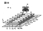
- 1A and 1B are diagrams for explaining a configuration example of a semiconductor device.
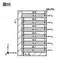
- 2A and 2B are diagrams for explaining a configuration example of the semiconductor device.
- 3A, 3B and 3C are diagrams for explaining a configuration example of a semiconductor device.
- FIG. 4 is a diagram illustrating a configuration example of the semiconductor device.
- 5A, 5B and 5C are diagrams for explaining a configuration example of the semiconductor device.
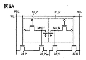
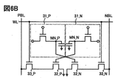
- 6A and 6B are diagrams for explaining a configuration example of the semiconductor device.
- 7A and 7B are diagrams for explaining a configuration example of the semiconductor device.
- 8A and 8B are diagrams for explaining a configuration example of the semiconductor device.
- 9A and 9B are diagrams for explaining a configuration example of the semiconductor device.
- FIG. 10A and 10B are diagrams for explaining a configuration example of the semiconductor device.
- FIG. 11 is a diagram illustrating a configuration example of the semiconductor device.
- FIG. 12 is a diagram illustrating a configuration example of the CPU.
- 13A and 13B are diagrams for explaining a configuration example of a CPU.
- FIG. 14 is a diagram illustrating a configuration example of a CPU.
- FIG. 15 is a diagram showing a configuration example of a semiconductor device.
- 16A and 16B are diagrams showing a configuration example of a transistor.
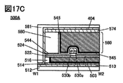
- 17A to 17C are diagrams showing a configuration example of a transistor.
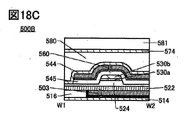
- 18A to 18C are diagrams showing a configuration example of a transistor.
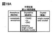
- FIG. 19A is a diagram illustrating the classification of the crystal structure of IGZO.
- FIG. 19A is a diagram illustrating the classification of the crystal structure of IGZO.
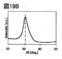
- FIG. 19B is a diagram illustrating an XRD spectrum of a CAAC-IGZO film.
- FIG. 19C is a diagram for explaining the microelectron diffraction pattern of the CAAC-IGZO film.
- FIG. 20 is a diagram illustrating a configuration example of an integrated circuit.
- 21A and 21B are diagrams illustrating a configuration example of an integrated circuit.
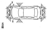
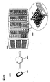
- 22A and 22B are diagrams illustrating application examples of integrated circuits.
- 23A and 23B are diagrams illustrating application examples of integrated circuits.
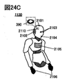
- 24A, 24B and 24C are diagrams illustrating application examples of integrated circuits.
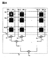
- FIG. 25 is a diagram illustrating an application example of an integrated circuit.
- FIG. 26 is a diagram for explaining an embodiment.
- the ordinal numbers “1st”, “2nd”, and “3rd” are added to avoid confusion of the components. Therefore, the number of components is not limited. Moreover, the order of the components is not limited. Further, for example, the component referred to in “first” in one of the embodiments of the present specification and the like is defined as another embodiment or the component referred to in “second” in the scope of claims. It is possible. Further, for example, the component mentioned in “first” in one of the embodiments of the present specification and the like may be omitted in another embodiment or in the claims.
- the power supply potential VDD may be abbreviated as potential VDD, VDD, etc. This also applies to other components (eg, signals, voltages, circuits, elements, electrodes, wiring, etc.).
- the code is used for identification such as "_1”, “_2”, “[n]", “[m, n]”. May be added and described.
- the second wiring GL is described as wiring GL [0].
- the semiconductor device refers to all devices that can function by utilizing the semiconductor characteristics.
- a semiconductor device such as a transistor, a semiconductor circuit, an arithmetic unit, and a storage device are one aspect of the semiconductor device. It may be said that a display device (liquid crystal display device, light emission display device, etc.), projection device, lighting device, electro-optical device, power storage device, storage device, semiconductor circuit, image pickup device, electronic device, and the like have a semiconductor device.
- the CPU 10 has a CPU core 11 and a backup circuit 12.
- the accelerator 20 has a drive circuit 15, an arithmetic processing unit 21, and memory units 22_1 to 22_N (N is a natural number).
- the drive circuit 15 is a circuit for driving the memory unit 22.
- the arithmetic processing unit 21 has arithmetic circuits 23_1 to 23_N.
- the drive circuit 15 is a circuit for driving the memory units 22_1 to 22_N and the arithmetic processing unit 21.
- the memory units 22_1 to 22_N each have a memory circuit 24.
- the memory units 22_1 to 22_N may be referred to as device memory or shared memory.
- the memory circuit 24 has a transistor 25 having a semiconductor layer 29 having a channel forming region.
- the CPU 10 has a function of performing general-purpose processing such as execution of an operating system, control of data, execution of various operations and programs.
- the CPU 10 has a CPU core 11.
- the CPU core 11 corresponds to one or more CPU cores.
- the CPU 10 has a backup circuit 12 capable of holding data in the CPU core 11 even when the supply of the power supply voltage is stopped.
- the supply of the power supply voltage can be controlled by electrical disconnection from the power supply domain (power domain) by a power switch or the like.
- the power supply voltage may be referred to as a drive voltage.
- the backup circuit 12 for example, a memory having a transistor (OS transistor) having an oxide semiconductor (Oxide Semiconductor) in the channel forming region is suitable.
- the backup circuit 12 composed of the OS transistor can be provided so as to be stacked with the CPU core 11 which can be configured by Si CMOS. Since the area of the backup circuit 12 is smaller than the area of the CPU core 11, the backup circuit 12 can be arranged on the CPU core without increasing the circuit area.
- the backup circuit 12 has a function of holding register data of the CPU core 11.
- the backup circuit 12 is also referred to as a data holding circuit.
- the accelerator 20 has a function of executing a program (also called a kernel or a kernel program) called from a host program.
- the accelerator 20 can perform, for example, parallel processing of matrix operations in graphic processing, parallel processing of product-sum operations of neural networks, parallel processing of floating-point operations in scientific and technological calculations, and the like.
- the memory units 22_1 to 22_N have a function of storing data processed by the accelerator 20. Specifically, the weight data W 1 to W N used for parallel processing of the product-sum operation of the neural network can be stored.
- the weight data W 1 to W N are data represented by three values of "+1", "0", or "-1" used for TNN.
- the memory circuit 24 included in the memory units 22_1 to 22_N has a function of holding the three-valued data by holding the two-valued voltage value in the two data-holding units. It should be noted that the data is not limited to three values, and data of four or more values can be used.
- the arithmetic processing unit 21 and the memory units 22_1 to 22_N are connected via the bit line PBL and the bit line NBL. Any one of the memory units 22_1 to 22_N has a pair of bit wire PBLs and a memory circuit 24 connected to the bit wire NBLs.
- the pair of bit line PBL and bit line NBL may be abbreviated as bit line BL.
- the pair of bit wire PBL and bit wire NBL are connected to any one of the arithmetic circuits 23_1 to 23_N, respectively.
- a pair of bit lines PBL and the bit line NBL are all the weight data W 1 to W N from the memory unit 22 (any one of the memory portion 22_1 to 22_N that memory unit 22) operation circuit 23 (the arithmetic circuit 23_1 to 23_N It is a wiring for giving one to the arithmetic circuit 23).
- the drive circuit 15 and the arithmetic processing unit 21 are connected via a data input line A IN.
- Arithmetic circuits 23_1 to any one of 23_N is any one of the input data A 1 to A N via a data input line A IN is supplied.
- Input data A 1 to A N is the data expressed by two values of "+1" or "-1" used to TNN.
- Data input line A IN is a wiring for providing input data A 1 to A N to the arithmetic circuit 23.
- the semiconductor layer 29 included in the transistor 25 is an oxide semiconductor. That is, the transistor 25 is an OS transistor.
- the memory circuit 24 is preferably a memory having an OS transistor (hereinafter, also referred to as an OS memory).
- the OS memory has a function of holding an electric charge according to a voltage value by putting an OS transistor in a non-conducting state.
- the OS transistor Since the bandgap of the metal oxide is 2.5 eV or more, the OS transistor has a minimum off current. As an example, voltage 3.5V between the source and the drain, at at room temperature (25 °C), 1 ⁇ less than 10 -20 A state current per channel width 1 [mu] m, less than 1 ⁇ 10 -22 A, or 1 ⁇ 10 It can be less than -24A. That is, the on / off current ratio of the drain current can be set to 20 digits or more and 150 digits or less. Therefore, the OS memory has an extremely small amount of electric charge leaked from the holding node via the OS transistor. Therefore, since the OS memory can function as a non-volatile memory circuit, power gating of the accelerator becomes possible.
- High-density integrated semiconductor devices may generate heat due to the driving of circuits. Due to this heat generation, the temperature of the transistor rises, and the characteristics of the transistor change, which may cause a change in field effect mobility and a decrease in operating frequency. Since the OS transistor has a higher thermal resistance than the Si transistor, the change in the field effect mobility due to the temperature change is unlikely to occur, and the operating frequency is also unlikely to decrease. Further, the OS transistor tends to maintain the characteristic that the drain current increases exponentially with respect to the gate-source voltage even when the temperature rises. Therefore, by using the OS transistor, stable operation can be performed in a high temperature environment.
- the metal oxides applied to the OS transistor are Zn oxide, Zn-Sn oxide, Ga-Sn oxide, In-Ga oxide, In-Zn oxide, and In-M-Zn oxide (M is: One or more selected from Ti, Ga, Y, Zr, La, Ce, Nd, Sn or Hf) and the like.
- M is: One or more selected from Ti, Ga, Y, Zr, La, Ce, Nd, Sn or Hf
- M is: One or more selected from Ti, Ga, Y, Zr, La, Ce, Nd, Sn or Hf
- oxides containing indium and zinc include aluminum, gallium, yttrium, copper, vanadium, beryllium, boron, silicon, titanium, iron, nickel, germanium, zirconium, molybdenum, lanthanum, cerium, neodymium, hafnium, tantalum, and tungsten. , One or more selected from magnesium and the like may be included.
- the metal oxide applied to the semiconductor layer is preferably a metal oxide having a crystal portion such as CAAC-OS, CAC-OS, and nc-OS.
- CAAC-OS is an abbreviation for c-axis-aligned crystalline oxide semiconductor ductor.
- CAC-OS is an abbreviation for Cloud-Aligned Composite oxide semiconductor.
- nc-OS is an abbreviation for nanocrystalline oxide semiconductor.
- CAAC-OS has a c-axis orientation and has a distorted crystal structure in which a plurality of nanocrystals are connected in the ab plane direction.
- the strain refers to a region in which a plurality of nanocrystals are connected in which the orientation of the lattice arrangement changes between a region in which the lattice arrangement is aligned and a region in which another lattice arrangement is aligned.
- the CAC-OS has a function of allowing electrons (or holes) to flow as carriers and a function of not allowing electrons (or holes) as carriers to flow. By separating the function of flowing electrons and the function of not flowing electrons, both functions can be maximized. That is, by using CAC-OS in the channel formation region of the OS transistor, both a high on-current and an extremely low off-current can be realized.
- OS transistors Since metal oxides have a large bandgap, electrons are less likely to be excited, and the effective mass of holes is large, OS transistors may be less likely to undergo avalanche breakdown than general Si transistors. .. Therefore, for example, hot carrier deterioration caused by avalanche breakdown can be suppressed. Since hot carrier deterioration can be suppressed, the OS transistor can be driven with a high drain voltage.
- the OS transistor is a storage type transistor that has a large number of electrons as carriers. Therefore, the influence of DIBL (Drain-Induced Barrier Lowering), which is one of the short-channel effects, is smaller than that of an inverting transistor (typically, a Si transistor) having a pn junction. That is, the OS transistor has a higher resistance to the short channel effect than the Si transistor.
- DIBL Drain-Induced Barrier Lowering
- the OS transistor Since the OS transistor has high resistance to the short channel effect, the channel length can be reduced without deteriorating the reliability of the OS transistor. Therefore, the degree of circuit integration can be increased by using the OS transistor.
- the drain electric field becomes stronger as the channel length becomes finer, but as mentioned above, the OS transistor is less likely to undergo avalanche breakdown than the Si transistor.
- the gate insulating film can be made thicker than that of the Si transistor. For example, even in a fine transistor having a channel length and a channel width of 50 nm or less, it may be possible to provide a thick gate insulating film of about 10 nm. By thickening the gate insulating film, the parasitic capacitance can be reduced, so that the operating speed of the circuit can be improved. Further, by making the gate insulating film thicker, the leakage current through the gate insulating film is reduced, which leads to a reduction in static current consumption.
- the accelerator 20 since the accelerator 20 has the memory circuit 24 which is the OS memory, the data can be held even if the supply of the power supply voltage is stopped. Therefore, the power gating of the accelerator 20 becomes possible, and the power consumption can be significantly reduced.
- the memory circuit 24 composed of the OS transistor can be provided so as to be stacked with the arithmetic circuit 23 that can be configured by Si CMOS. Therefore, the circuit area can be arranged without increasing the circuit area.
- the memory circuit 24 preferably has a NOSRAM circuit configuration.
- NOSRAM registered trademark
- NOSRAM is an abbreviation for "Nonvolatile Oxide Semiconductor RAM”.
- NOSRAM refers to a memory in which the memory cell is a 2-transistor type (2T) or 3-transistor type (3T) gain cell and the access transistor is an OS transistor.
- the OS transistor has an extremely small leakage current, that is, a current flowing between the source and the drain in the off state.
- the NOSRAM can be used as a non-volatile memory by holding the electric charge corresponding to the data in the memory circuit by using the characteristic that the leakage current is extremely small.
- NO SRAM can read the held data without destroying it (non-destructive reading), it is suitable for parallel processing of the product-sum operation of a neural network in which only the data reading operation is repeated in large quantities.
- the arithmetic processing unit 21 has a function of performing arithmetic processing using digital values. Digital values are less susceptible to noise. Therefore, the accelerator 20 is suitable for performing arithmetic processing that requires highly accurate arithmetic results.
- the arithmetic processing unit 21 is preferably composed of Si CMOS, that is, a transistor (Si transistor) having silicon in the channel forming region. With this configuration, it can be provided by stacking with an OS transistor.
- the drive circuit 15 has a function for causing the memory units 22_1 to 22_N to hold weight data. Further, the drive circuit 15 has a function of giving input data to the arithmetic circuits 23_1 to 23_N to execute a product-sum operation of the neural network or the like.
- the memory circuit 24 composed of the OS transistor and the arithmetic circuits 23_1 to 23_N are provided with a bit line NBL extending in a direction substantially perpendicular to the substrate surface on which the drive circuit 15 and the arithmetic circuits 23_1 to 23_N are provided. It is electrically connected via a bit wire PBL.
- approximately vertical means a state in which the objects are arranged at an angle of 85 degrees or more and 95 degrees or less.
- the X direction, the Y direction, and the Z direction shown in FIG. 1B and the like are directions that are orthogonal to each other or intersect with each other. Further, the X direction and the Y direction are parallel or substantially parallel to the substrate surface, and the Z direction is perpendicular or substantially perpendicular to the substrate surface.
- Arithmetic circuits 23_1 to 23_N uses the input data A 1 to A N and weight data W 1 through W N, integer operations, a single-precision floating-point operation, one function for one of the processing such as double-precision floating-point arithmetic Has.
- the arithmetic circuit 23 has a function of repeatedly executing the same processing such as a product-sum operation.
- the arithmetic circuits 23_1 to 23_N are configured to provide one arithmetic circuit 23 for each bit line NBL and bit line PBL of the memory circuit 24, that is, for each row (Column) (Column-Parallel Calibration).
- the data for one line (up to all bit lines) of the memory circuit 24 can be processed in parallel.
- the data bus size between the CPU and the memory is not limited. Therefore, in the Colon-Parallel Calction, the degree of parallelism of the calculation can be significantly increased.
- the semiconductor layer of the transistors constituting the circuit is silicon.
- a transistor having silicon as a semiconductor layer is called a Si transistor.
- the Si transistor is preferably formed by using an SOI substrate having an insulating layer (also referred to as a BOX layer) formed by embedding oxide in a silicon substrate and single crystal silicon on the insulating layer.
- the silicon substrate is, for example, a p-type single crystal silicon substrate.
- a well region to which an impurity element that imparts conductivity is added can be overlapped on the silicon substrate in the region where the Si transistor is provided.
- the well region can function as a bottom gate electrode by independently changing the potential of the well region. Therefore, the threshold voltage of the Si transistor can be controlled.
- the threshold voltage of the Si transistor can be made larger and the off-current can be reduced. Therefore, by applying a negative potential to the well region, the drain current when the potential applied to the gate electrode of the Si transistor is 0 V can be reduced.
- the variation in the threshold voltage can be reduced and the power supply voltage can be lowered. As a result, the power consumption in the arithmetic circuits 23_1 to 23_N can be reduced, and the arithmetic efficiency can be improved.
- the bus 30 electrically connects the CPU 10 and the accelerator 20. That is, the CPU 10 and the accelerator 20 can transmit data via the bus 30.
- FIG. 2A is a schematic view of the schematic view of FIG. 1B as viewed from the z direction.
- six arithmetic circuits 23_1 to 23_1 are arranged side by side in the y direction, and six memory units 22_1 to 22_6 are shown so as to overlap in the z direction.
- FIG. 2A illustrates a drive circuit 15 that supplies input data A 1 to A 6 to the six arithmetic circuits 23_1 to 23_6 via the data input line A IN.
- the arithmetic circuits 23_1 to 23_6 are connected to the memory units 22_1 to 22_6 by bit lines NBL and PBL (indicated by one opening in FIG. 2A), respectively. That is, it is shown that they are connected via wiring extending in the z direction. That is, the arithmetic circuits 23_1 to 23_6 and the memory units 22_1 to 22_6 can be arranged at a short distance by the bit lines NBL and PBL. Therefore, the parasitic capacitance between the bit wires NBL and PBL and other elements can be reduced. Therefore, it is possible to reduce the electric charge due to the charging and discharging of the bit wire, and it is possible to reduce the power consumption and improve the calculation efficiency.
- the transistors of the memory units 22_1 to 22_6 are OS transistors, they can be stacked on the arithmetic circuits 23_1 to 23_1 composed of Si transistors. Therefore, since the arithmetic circuit and the memory unit can be arranged so as to overlap each other, the circuit area can be reduced by the amount that the memory unit is arranged and increased. Therefore, the semiconductor device can be miniaturized. In addition, the data input line A IN extending from the drive circuit 15 can be shortened.
- FIG. 2B a schematic diagram in the case where the arithmetic circuits 23_1 to 23_6 and the memory units 22_1 to 22_6 are alternately arranged side by side in the y direction is shown in the same manner as in FIG. 2A.
- the example of FIG. 2B is a case where the memory circuit is composed of Si transistors so that the data holding circuit of the memory circuit is SRAM (Static RAM). Therefore, as shown in FIG. 2A, the arithmetic processing unit and the memory unit are not arranged in an overlapping manner, but are arranged side by side on a plane.
- the arithmetic circuits 23_1 to 23_6 are connected by bit lines NBL and PBL (shown as one wiring in FIG. 2A) extending from the adjacent memory units 22_1 to 22_6, respectively. That is, it is shown that they are connected via wiring extending in the y direction. That is, the arithmetic circuits 23_1 to 23_6 and the memory units 22_1 to 22_6 can be arranged at a longer distance than in the z direction by the bit lines NBL and PBL. Therefore, the parasitic capacitance between the bit wires NBL and PBL and other elements increases. Therefore, the electric charge due to charging and discharging of the bit wire increases. Therefore, it can be said that the configuration of one aspect of the present invention illustrated in FIG. 2A is excellent in miniaturization and low power consumption.
- One aspect of the present invention can provide a miniaturized semiconductor device in a semiconductor device including an accelerator and a CPU.
- one aspect of the present invention can provide a semiconductor device having reduced power consumption in a semiconductor device including an accelerator and a CPU.
- one aspect of the present invention can provide a semiconductor device in which the number of data transfers in the CPU is reduced.
- a semiconductor device having a new configuration can be provided.
- the semiconductor device of one aspect of the present invention has a non-Von Neumann architecture, and can perform parallel processing with extremely low power consumption as compared with the von Neumann architecture in which the power consumption increases as the processing speed increases. ..
- FIG. 3A is a diagram for explaining the relationship between the processing capacity (OPS: Operations Per Second) and the power consumption (W).
- OPS Operations Per Second
- W power consumption
- the vertical axis represents the processing capacity
- the horizontal axis represents the power consumption.
- 0.1 TOPS / W Trip Operations Per Second / W
- 1 TOPS / W 10 TOPS / W
- 100 TOPS / W 100 TOPS / W
- 1 POPS / W Pera Operations Per Second / W
- the region 910 shows the region including the conventional general-purpose AI accelerator (Von Neumann type), and the region 912 shows the region including the semiconductor device of one aspect of the present invention.
- the area 910 includes, for example, a CPU (Central Processing Unit), a GPU (Graphics Processing Unit), an FPGA (Field-Programmable Gate Array), and the like.
- the semiconductor device of one aspect of the present invention by applying the semiconductor device of one aspect of the present invention, it is possible to reduce the power consumption by about two orders of magnitude as compared with the conventional general-purpose AI accelerator (Von Neumann type), and to improve the processing performance. It can be significantly improved (for example, 1000 times or more).
- a calculation efficiency of 100 TOPS / W or more can be expected.
- FIG. 3B shows an image diagram of the power consumption of the semiconductor device having the conventional configuration in image recognition
- FIG. 3C shows an image diagram of the power consumption of the semiconductor device using the configuration of one aspect of the present invention in image recognition.
- the vertical axis represents electric power and the horizontal axis represents time.
- the electric power 914 indicates the leak power
- the electric power 916 indicates the CPU power (CPU power consumption)
- the electric power 918 indicates the memory power.
- the electric power 914 indicates the leak electric power
- the electric power 920 indicates the CPU electric power
- the electric power 922 indicates the accelerator power (power consumption of the accelerator).
- the electric power 922 also includes the electric power used for the arithmetic circuit and the memory circuit.
- the arrows a, b, and c represent signals in image recognition, respectively. It is assumed that the semiconductor device starts arithmetic processing such as image recognition when the signals of the arrows a, b, and c are input.
- a constant leakage power (power 914) is generated with respect to time.
- the leakage power (power) while using the CPU power (power 920) and the accelerator power (power 922). 914) is generated, but during the period when the CPU power (power 920) and the accelerator power (power 922) are not used, the leak power (power 914) does not occur during the normally-off drive (the period shown in FIG. 3C). It can be t1). This makes it possible to significantly reduce power consumption. That is, it is possible to provide a semiconductor device having extremely low power consumption.
- FIG. 4 shows a DRAM (Dynamic) such as a NO SRAM, a CPU (Central Processing Unit), a GPU (Graphics Processing Unit), and an FPGA (Field-Programmable Gate Array) included in the semiconductor device of one aspect of the present invention described in FIG. 3A.
- DRAM Dynamic
- CPU Central Processing Unit
- GPU Graphics Processing Unit
- FPGA Field-Programmable Gate Array
- the flash memory is excellent in relative cost per 1 Gbit, the read energy is as high as 100 pJ. Further, although the relative cost per 1 Gbit of the DRAM is inferior to that of the flash memory, the read energy is small. Further, although the relative cost per 1 Gbit of SRAM is significantly inferior to that of DRAM and flash memory, the read energy is significantly smaller.
- the NO SRAM included in the semiconductor device of one aspect of the present invention with respect to these flash memories, DRAMs, and SRAMs has extremely low read energy and is superior in relative cost per 1 Gbit as compared with SRAMs. Therefore, it can be said that a semiconductor device having a NO SRAM is suitable when aiming for a calculation efficiency exceeding 100 TOPS / W as described with reference to FIG. 3A.
- FIG. 5A is a diagram illustrating an example of a circuit configuration applicable to the memory units 22_1 to 22_N included in the semiconductor device 100 of the present invention.
- the bit lines PBL_1 to PBL_N, the bit lines NBL_1 to NBL_N, and the word lines WL_1 to WL_M (M is a natural number) arranged side by side in the matrix direction of M rows and N columns (M and N are natural numbers of 2 or more) are shown. Shown. Further, the memory circuit 24 connected to each word line and bit line is illustrated.
- FIG. 5B is a diagram illustrating a circuit configuration example applicable to the memory circuit 24.
- the memory circuit 24 includes a data holding circuit 31_P, a data holding circuit 31_N, a transistor 32_P, a transistor 32_N, a transistor 33_P, and a transistor 33_N.
- each transistor in the memory circuit 24 may have a back gate.
- the back gate may be connected to the gate, or may be configured to give a potential different from that of the gate to control the electrical characteristics of the transistor.
- the data holding circuit 31_P is connected to the wiring node MN_P connected to the gate of the transistor 32_P.
- One of the source and drain of transistor 32_P is connected to a fixed potential such as GND.
- One of the source or drain of transistor 33_P is connected to the other of the source or drain of transistor 32_P.
- One of the source and drain of transistor 33_P is connected to the bit line PBL.
- the gate of transistor 33_P is connected to the word line WL.
- the data holding circuit 31_N is connected to the wiring node MN_N connected to the gate of the transistor 32_N.
- One of the source and drain of transistor 32_N is connected to a fixed potential such as GND.
- One of the source or drain of transistor 33_N is connected to the other of the source or drain of transistor 32_N.
- One of the source and drain of transistor 33_N is connected to the bit line NBL.
- the gate of transistor 33_N is connected to the word line WL.
- the data holding circuit 31_P and the data holding circuit 31_N each have a function of holding a signal corresponding to an H level or L level voltage.
- FIG. 5C illustrates the circuit configuration of the data holding circuit 31_P and the data holding circuit 31_N applicable to the data holding circuit 31_P of FIG. 5B.
- Each transistor illustrated in FIG. 5C is an OS transistor.
- the OS transistor has an extremely small leakage current, that is, a current flowing between the source and the drain in the off state.
- the NOSRAM can be used as a non-volatile memory by holding the electric charge corresponding to the data in the node MN in the memory circuit 24 by using the characteristic that the leakage current is extremely small.
- the voltage of the node MN is the voltage held by the data holding circuit 31.
- the voltage held in the data holding circuit 31 is given by the signal MBL.
- the signal MBL may be configured to be written to the node MN at the timing of controlling the signal MWL given to the gate of the transistor 34.
- the NO SRAM of the 3-transistor type (3T) gain cell can hold a voltage of two or more values such as a five-value or a seven-value.
- FIG. 6A shows the circuit configuration of the memory circuit 24 in which the circuit configuration of the data holding circuit 31 of FIG. 5C is applied to FIG. 5B.
- the truth table of each signal illustrated in FIG. 6A is as shown in Table 1.
- Table 1 the H level and L level voltages are represented by logics "1" and "0".
- Cell P corresponds to the logic corresponding to the voltage held by the node MN_P, that is, the data holding circuit 31_P.
- Cell N corresponds to the logic corresponding to the voltage held by the node MN_N, that is, the data holding circuit 31_N.
- “W” is data determined by the logic of bit lines NBL and PBL, and is data represented by three values of “0”, “+1” or “-1” used for TNN. The prohibition is indicated by "x”.
- FIG. 6A can be transformed into the circuit configuration of FIG. 7A.
- the transistors 33_P and 33_N are replaced with transistors 34, and each wiring and the connection between the transistors are changed.
- the data of the truth table shown in Table 1 can be obtained.
- FIG. 6B can be transformed into the circuit configuration of FIG. 7B.
- the transistors 33_P and 33_N are replaced with transistors 34, and each wiring and the connection between the transistors are changed.
- the data of the truth table shown in Table 2 can be obtained.
- FIG. 8A is a diagram illustrating an example of a circuit configuration applicable to the arithmetic processing unit 21 included in the semiconductor device 100 of the present invention.
- the arithmetic processing unit 21 has arithmetic circuits 23_1 to 23_N.
- the N arithmetic circuits 23_1 to 23_N are given to any one of N bit lines PBL_1 to bit line PBL_N, any one of N bit lines NBL_1 to bit line NBL_N, and data input line A IN , respectively. and any one of the input data a 1 to a N, the respective signals are input, and outputs an output signal Q_1 to Q_n.
- the output signals Q_1 to Q_N correspond to data obtained by performing a product-sum operation using the data held in the memory circuit 24 and the data input from the drive circuit 15 via the data input line A IN.
- FIG. 8B is a diagram illustrating a circuit configuration example of the arithmetic circuit 23 applicable to the arithmetic circuit 23_1 to the arithmetic circuit 23_N.
- FIG. 8B is a circuit for executing arithmetic processing based on the TNN architecture.
- the arithmetic circuit 23 includes a logic circuit 42 for performing a product-sum operation, an accumulator 43, a latch circuit 44, and a coding circuit 45 for outputting an output signal Q.
- the logic circuit 42 includes any one of N bit lines PBL_1 to bit line PBL_N (data PBL in the figure), any one of N bit lines NBL_1 to bit line NBL_N (data NBL in the figure), and data.
- data a any one of the input data a 1 to a N is applied to the input lines a iN, each signal is inputted.
- Data (data W) represented by three values of "0", “+1” or “-1” from data PBL and data NBL, and data A represented by two values of "+1” or “-1”.
- the same product of M pieces and their sum can be executed in N parallel ⁇ 1 bit ⁇ M / N line, so that an M / N clock is required. Therefore, in the configurations of FIGS. 8A and 8B, the calculation time can be shortened by executing the product-sum calculation in parallel, so that the calculation efficiency can be improved.
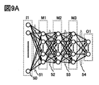
- FIG. 9A illustrates a hierarchical neural network.
- FIG. 9A illustrates a fully connected neural network of a neuron 50, an input layer 1 layer (I1), an intermediate layer 3 layers (M1 to M3), and an output layer 1 layer (O1).
- the number of neurons in the input layer I1 is 786
- the number of neurons in the intermediate layers M1 to M3 is 256
- the number of neurons in the output layer O1 is 10
- the number of connections in each layer (layer 51, layer 52, layer 53 and layer 54) is ( 786 x 256) + (256 x 256) + (256 x 256) + (256 x 10), for a total of 334,336 pieces. That is, since the weight parameters required for the neural network calculation are about 330 Kbits in total, the memory capacity can be sufficiently implemented even in a small-scale system.
- FIG. 9B shows a detailed block diagram of the semiconductor device 100 capable of calculating the neural network shown in FIG. 9A.
- FIG. 9B the arithmetic processing unit 21, the arithmetic circuit 23 corresponding to the arithmetic circuits 23_1 to 23_N, the memory unit 22 corresponding to the memory units 22_1 to 22_N, the memory circuit 24, and the bit line NBL described with reference to FIGS. 1A and 1B are shown.
- PBL a configuration example of the drive circuit 15 shown in FIGS. 1A and 1B is shown.
- FIG. 9B the controller 61, the row decoder 62, the word line driver 63, the column decoder 64, the write driver 65, the precharge circuit 66, the input buffer 71, and the configuration corresponding to the drive circuit 15 described with reference to FIGS. 1A and 1B.
- the arithmetic control circuit 72 is shown in the figure.
- FIG. 10A is a diagram in which blocks for controlling the memory unit 22 are extracted for each configuration shown in FIG. 9B.
- the controller 61, the row decoder 62, the word line driver 63, the column decoder 64, the write driver 65, and the precharge circuit 66 are extracted and shown.
- the controller 61 processes an input signal from the outside to generate a control signal for the row decoder 62 and the column decoder 64.
- the input signal from the outside is a control signal for controlling the memory unit 22 such as a write enable signal and a read enable signal. Further, the controller 61 inputs / outputs data written to the memory unit 22 or data read from the memory unit 22 via the bus with the CPU 10.
- the low decoder 62 generates a signal for driving the word line driver 63.
- the word line driver 63 generates a signal given to the word line WL in addition to the signal MWL given to the data holding circuits 31_P and 31_N.
- the column decoder 64 generates a signal for driving the write driver 65.
- the write driver 65, a data holding circuit 31_P, other signals MBL given to 31_n, to generate the input data A 1 to A N is applied to the data input lines A IN.
- the precharge circuit 66 has a function of precharging bit lines NBL, PBL, and the like.
- the signal read from the memory circuit 24 of the memory unit 22 is input to the arithmetic circuit 23 via the bit lines NBL and PBL.
- FIG. 10B is a diagram in which blocks for controlling the arithmetic processing unit 21 are extracted for each configuration shown in FIG. 9B.
- the controller 61 processes an input signal from the outside to generate a control signal of the arithmetic control circuit 72. Further, the controller 61 generates various signals such as a clock signal for controlling the arithmetic circuit 23 included in the arithmetic processing unit 21.
- the arithmetic control circuit 72 in response to the output of the control and the input buffer 71 of the controller 61, generates the input data A 1 to A N is applied to the data input lines A IN.
- the arithmetic processing unit 21 reinputs the data related to the arithmetic result into the arithmetic processing unit 21 via the input buffer 71 and the arithmetic control circuit 72.
- the arithmetic processing unit 21 processes the data according to the arithmetic result by using the buffer memory in the input buffer 71, so that the data in the middle of the arithmetic is not read into the main memory or the like outside the accelerator, and the data bus of the CPU is used. Parallel calculation of the number of bits larger than the width becomes possible. Further, since the number of times that a huge number of weight parameters are transferred to and from the CPU 10 can be reduced, power consumption can be reduced.
- one aspect of the present invention can provide a miniaturized semiconductor device in a semiconductor device including an accelerator and a CPU.
- one aspect of the present invention can provide a semiconductor device having reduced power consumption in a semiconductor device including an accelerator and a CPU.
- one aspect of the present invention can provide a semiconductor device in which the number of data transfers in the CPU is reduced.
- a semiconductor device having a new configuration can be provided.
- FIG. 11 is a diagram illustrating an example of operation when a part of the calculation of the program executed by the CPU is executed by the accelerator.
- the host program is executed on the CPU (step S1).
- step S2 When the CPU confirms the instruction to secure the data area required for performing the calculation using the accelerator in the memory unit (step S2), the CPU allocates the data area in the memory unit (step S2). S3).
- the CPU transmits input data from the main memory to the memory unit (step S4).
- the memory unit receives the input data and stores the input data in the area secured in step S2 (step S5).
- step S6 When the CPU confirms the instruction to start the kernel program (step S6), the accelerator starts the execution of the kernel program (step S7).
- the CPU may be switched from the state of performing calculation to the state of PG (step S8). In that case, the CPU is switched from the PG state to the state of performing the calculation just before the accelerator finishes the execution of the kernel program (step S9).
- the CPU By putting the CPU in the PG state during the period from step S8 to step S9, the power consumption and heat generation of the semiconductor device as a whole can be suppressed.
- step S10 When the accelerator finishes executing the kernel program, the output data is stored in the above memory section (step S10).
- step S11 After the execution of the kernel program is completed, when the CPU confirms the instruction to transmit the output data stored in the memory unit to the main memory (step S11), the above output data is transmitted to the above main memory, and the above It is stored in the main memory (step S12).
- step S13 When the CPU confirms the instruction to release the data area reserved on the memory unit (step S13), the area reserved on the memory unit is released (step S14).
- step S1 By repeating the above operations from step S1 to step S14, a part of the calculation executed by the CPU can be executed by the accelerator while suppressing the power consumption and heat generation of the CPU and the accelerator.
- FIG. 12 shows a configuration example of the CPU 10.
- the CPU 10 includes a CPU core (CPU Core) 200, an L1 (level 1) cache memory device (L1 cache) 202, an L2 cache memory device (L2 cache) 203, a bus interface unit (Bus I / F) 205, and a power switch 210 ⁇ . It has 212, a level shifter (LS) 214.
- the CPU core 200 has a flip-flop 220.
- the CPU core 200, the L1 cache memory device 202, and the L2 cache memory device 203 are connected to each other by the bus interface unit 205.
- the PMU193 generates a clock signal GCLK1 and various PG (power gating) control signals (PG control signals) in response to signals such as interrupt signals (Interrupts) input from the outside and signal SLEEP1 issued by the CPU 10.
- the clock signals GCLK1 and PG control signals are input to the CPU 10.
- the PG control signal controls the power switches 210 to 212 and the flip-flop 220.
- the power switches 210 and 211 control the supply of voltages VDDD and VDD1 to the virtual power supply line V_ VDD (hereinafter referred to as V_ VDD line), respectively.
- the power switch 212 controls the supply of the voltage VDDH to the virtual power supply line V_VDH (hereinafter, referred to as V_VDH line).
- the voltage VSSS is input to the CPU 10 and the PMU 193 without going through the power switch.
- the voltage VDDD is input to the PMU 193 without going through the power switch.
- Voltages VDDD and VDD1 are drive voltages for CMOS circuits.
- the voltage VDD1 is lower than the voltage VDDD and is a driving voltage in the sleep state.
- the voltage VDDH is a drive voltage for the OS transistor and is higher than the voltage VDDD.
- Each of the L1 cache memory device 202, the L2 cache memory device 203, and the bus interface unit 205 has at least one power gating capable power domain.
- a power domain capable of power gating is provided with one or more power switches. These power switches are controlled by a PG control signal.
- the flip-flop 220 is used as a register.
- the flip-flop 220 is provided with a backup circuit. Hereinafter, the flip-flop 220 will be described.
- FIG. 13A shows a circuit configuration example of the flip-flop 220 (Flip-flop).
- the flip-flop 220 has a scan flip-flop (Scan Flip-flop) 221 and a backup circuit (Backup Circuit) 222.
- the scan flip-flop 221 has nodes D1, Q1, SD, SE, RT, CK, and a clock buffer circuit 221A.
- Node D1 is a data (data) input node
- node Q1 is a data output node
- node SD is a scan test data input node.
- the node SE is an input node of the signal SCE.
- the node CK is an input node for the clock signal GCLK1.
- the clock signal GCLK1 is input to the clock buffer circuit 221A.
- the analog switch of the scan flip-flop 221 is connected to the nodes CK1 and CKB1 of the clock buffer circuit 221A.
- the node RT is an input node for a reset signal.
- the signal SCE is a scan enable signal and is generated by PMU193.
- PMU193 generates signals BK and RC.
- the level shifter 214 level-shifts the signals BK and RC to generate the signals BKH and RCH.
- the signals BK and RC are backup signals and recovery signals.
- the circuit configuration of the scan flip-flop 221 is not limited to FIG. Flip-flops provided in standard circuit libraries can be applied.
- the backup circuit 222 has nodes SD_IN, SN11, transistors M11 to M13, and a capacitive element C11.
- Node SD_IN is an input node for scan test data and is connected to node Q1 of scan flip-flop 221.
- the node SN11 is a holding node of the backup circuit 222.
- the capacitance element C11 is a holding capacitance for holding the voltage of the node SN11.
- Transistor M11 controls the conduction state between node Q1 and node SN11.
- the transistor M12 controls the conduction state between the node SN11 and the node SD.
- the transistor M13 controls the conduction state between the node SD_IN and the node SD.
- the on / off of the transistors M11 and M13 is controlled by the signal BKH, and the on / off of the transistors M12 is controlled by the signal RCH.
- Transistors M11 to M13 are OS transistors like the transistors of the data holding circuits 31_N and 31_P of the memory circuit 24 and the transistors 32_P, 32_N, 33_P, and 33_N described above.
- the transistors M11 to M13 are shown to have a back gate.
- the back gates of the transistors M11 to M13 are connected to a power line that supplies the voltage VBG1.
- the backup circuit 222 has a non-volatile characteristic because it can suppress a drop in the voltage of the node SN11 due to the feature of the OS transistor that the off-current is extremely small and consumes almost no power for holding data. Since the data is rewritten by charging / discharging the capacitive element C11, the backup circuit 222 is, in principle, not limited in the number of rewrites, and can write and read data with low energy.
- the backup circuit 222 can be laminated on the scan flip-flop 221 composed of the silicon CMOS circuit.
- the backup circuit 222 Since the backup circuit 222 has a very small number of elements as compared with the scan flip-flop 221, it is not necessary to change the circuit configuration and layout of the scan flip-flop 221 in order to stack the backup circuits 222. That is, the backup circuit 222 is a highly versatile backup circuit. Further, since the backup circuit 222 can be provided in the region where the scan flip-flop 221 is formed, the area overhead of the flip-flop 220 can be reduced to zero even if the backup circuit 222 is incorporated. Therefore, by providing the backup circuit 222 on the flip-flop 220, power gating of the CPU core 200 becomes possible. Since the energy required for power gating is small, it is possible to power gate the CPU core 200 with high efficiency.
- the backup circuit 222 By providing the backup circuit 222, the parasitic capacitance due to the transistor M11 is added to the node Q1, but since it is smaller than the parasitic capacitance due to the logic circuit connected to the node Q1, the scan flip-flop 221 operates. There is no effect. That is, even if the backup circuit 222 is provided, the performance of the flip-flop 220 is not substantially deteriorated.
- the low power consumption state of the CPU core 200 for example, a clock gating state, a power gating state, and a hibernation state can be set.
- the PMU193 selects the low power consumption mode of the CPU core 200 based on the interrupt signal, the signal SLEEP1, and the like. For example, when shifting from the normal operating state to the clock gating state, the PMU 193 stops generating the clock signal GCLK1.
- the PMU193 when shifting from the normal operating state to the hibernation state, the PMU193 performs voltage and / or frequency scaling. For example, when performing voltage scaling, the PMU 193 turns off the power switch 210 and turns on the power switch 211 in order to input the voltage VDD1 to the CPU core 200.
- the voltage VDD1 is a voltage that does not cause the data of the scan flip-flop 221 to be lost.
- PMU193 lowers the frequency of the clock signal GCLK1.
- FIG. 14 shows an example of the power gating sequence of the CPU core 200.
- t1 to t7 represent time.
- the signals PSE0 to PSE2 are control signals of the power switches 210 to 212, and are generated by the PMU193. When the signal PSE0 is “H” / “L”, the power switch 210 is on / off. The same applies to the signals PSE1 and PSE2.
- the PMU193 stops the clock signal GCLK1 and sets the signals PSE2 and BK to “H”.
- the level shifter 214 becomes active and outputs the “H” signal BKH to the backup circuit 222.
- the transistor M11 of the backup circuit 222 is turned on, and the data of the node Q1 of the scan flip-flop 221 is written to the node SN11 of the backup circuit 222. If the node Q1 of the scan flip-flop 221 is "L”, the node SN11 remains “L”, and if the node Q1 is "H”, the node SN11 becomes "H”.
- the PMU193 sets the signals PSE2 and BK to “L” at time t2 and sets the signal PSE0 to “L” at time t3.
- the state of the CPU core 200 shifts to the power gating state.
- the signal PSE0 may be lowered at the timing of lowering.
- PMU193 sets the signal PSE0 to “H” to shift from the power gating state to the recovery state.
- the PMU193 sets the signals PSE2, RC, and SCE to "H” in a state where charging of the V_ VDD line is started and the voltage of the V_ VDD line becomes VDDD (time t5).
- the transistor M12 is turned on, and the electric charge of the capacitive element C11 is distributed to the node SN11 and the node SD. If the node SN11 is "H”, the voltage of the node SD rises. Since the node SE is “H”, the data of the node SD is written to the input side latch circuit of the scan flip-flop 221. When the clock signal GCLK1 is input to the node CK at time t6, the data of the input side latch circuit is written to the node Q1. That is, the data of the node SN11 is written to the node Q1.
- PMU193 sets the signals PSE2, SCE, and RC to “L”, and the recovery operation ends.
- the backup circuit 222 using the OS transistor is very suitable for normal off computing because both dynamic and static low power consumption are small.
- the CPU 10 including the CPU core 200 having the backup circuit 222 using the OS transistor can be referred to as a NonfCPU (registered trademark).
- the Noff CPU has a non-volatile memory and can stop the power supply when the operation is not required. Even if the flip-flop 220 is mounted, the performance of the CPU core 200 can be reduced and the dynamic power can be hardly increased.
- the CPU core 200 may have a plurality of power domains capable of power gating.
- the plurality of power domains are provided with one or more power switches for controlling the voltage input.
- the CPU core 200 may have one or a plurality of power domains in which power gating is not performed.
- a power gating control circuit for controlling the flip-flop 220 and the power switches 210 to 212 may be provided in the power domain where power gating is not performed.
- the application of the flip-flop 220 is not limited to the CPU 10.
- the flip-flop 220 can be applied to a register provided in a power domain capable of power gating.
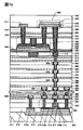
- FIG. 15 shows a part of the cross-sectional structure of the semiconductor device.
- the semiconductor device shown in FIG. 15 includes a transistor 550, a transistor 500, and a capacitive element 600.
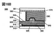
- FIG. 16A is a cross-sectional view of the transistor 500 in the channel length direction
- FIG. 16B is a cross-sectional view of the transistor 500 in the channel width direction.
- the transistor 500 corresponds to the transistors 32 to 34 shown in the above embodiment
- the transistor 550 corresponds to a Si transistor included in the arithmetic circuit 23.
- the capacitance element 600 corresponds to the capacitance element 35.
- Transistor 500 is an OS transistor.
- the OS transistor has an extremely small off current. Therefore, it is possible to hold the data voltage or electric charge written to the storage node via the transistor 500 for a long period of time. That is, the refresh operation frequency of the storage node (node MN) can be reduced, or the refresh operation is not required, so that the power consumption of the semiconductor device can be reduced.
- the transistor 500 is provided above the transistor 550, and the capacitive element 600 is provided above the transistor 550 and the transistor 500.
- the transistor 550 is provided on the substrate 311.
- the substrate 311 is, for example, a p-type silicon substrate.
- the substrate 311 may be an n-type silicon substrate.
- the oxide layer 314 is preferably an insulating layer (also referred to as a BOX layer) formed in a substrate 311 by buried oxidation, for example, silicon oxide.
- the transistor 550 is provided on a single crystal silicon, so-called SOI (Silicon On Insulator) substrate, which is provided on the substrate 311 via an oxide layer 314.
- SOI Silicon On Insulator
- the substrate 311 in the SOI substrate is provided with an insulator 313 that functions as an element separation layer.
- the substrate 311 also has a well region 312.
- the well region 312 is a region to which n-type or p-type conductivity is imparted depending on the conductive type of the transistor 550.
- the single crystal silicon in the SOI substrate is provided with a semiconductor region 315, a low resistance region 316a that functions as a source region or a drain region, and a low resistance region 316b. Further, the well layer 312 has a low resistance region 316c.
- the transistor 550 can be provided so as to be overlapped with the well region 312 to which the impurity element that imparts conductivity is added.
- the well region 312 can function as a bottom gate electrode of the transistor 550 by independently changing the potential via the low resistance region 316c. Therefore, the threshold voltage of the transistor 550 can be controlled.
- the threshold voltage of the transistor 550 can be made larger and the off-current can be reduced. Therefore, by applying a negative potential to the well region 312, the drain current when the potential applied to the gate electrode of the Si transistor is 0 V can be reduced.
- the power consumption based on the through current or the like in the arithmetic circuit 23 having the transistor 550 can be reduced, and the arithmetic efficiency can be improved.
- the transistor 550 is preferably of the so-called Fin type, in which the upper surface of the semiconductor layer and the side surface in the channel width direction are covered with the conductor 318 via the insulator 317.
- the on-characteristics of the transistor 550 can be improved by increasing the effective channel width. Further, since the contribution of the electric field of the gate electrode can be increased, the off characteristic of the transistor 550 can be improved.
- the transistor 550 may be either a p-channel type transistor or an n-channel type transistor.
- the conductor 318 may function as a first gate (also referred to as a top gate) electrode. Further, the well region 312 may function as a second gate (also referred to as a bottom gate) electrode. In that case, the potential applied to the well region 312 can be controlled via the low resistance region 316c.
- the low resistance region 316a that becomes the region where the channel of the semiconductor region 315 is formed, the region in the vicinity thereof, the source region, or the drain region, and the low resistance region 316b and the low resistance connected to the electrodes that control the potential of the well region 312.
- a semiconductor such as a silicon-based semiconductor
- it may be formed of a material having Ge (germanium), SiGe (silicon germanium), GaAs (gallium arsenide), GaAlAs (gallium aluminum arsenide), or the like.
- a configuration using silicon in which the effective mass is controlled by applying stress to the crystal lattice and changing the lattice spacing may be used.
- the transistor 550 may be a HEMT by using GaAs, GaAlAs, or the like.
- the low resistance region 316a, the low resistance region 316b, and the low resistance region 316c are elements that impart n-type conductivity such as arsenic and phosphorus, or boron. It contains an element that imparts p-type conductivity such as.
- the conductor 318 that functions as a gate electrode is a semiconductor material such as silicon, a metal material, or an alloy that contains an element that imparts n-type conductivity such as arsenic or phosphorus, or an element that imparts p-type conductivity such as boron.
- a material or a conductive material such as a metal oxide material can be used.
- a silicide such as nickel silicide may be used as the conductor 318.
- the threshold voltage of the transistor can be adjusted by selecting the material of the conductor. Specifically, it is preferable to use a material such as titanium nitride or tantalum nitride for the conductor. Further, in order to achieve both conductivity and embedding property, it is preferable to use a metal material such as tungsten or aluminum as a laminate for the conductor, and it is particularly preferable to use tungsten in terms of heat resistance.
- the low resistance region 316a, the low resistance region 316b, and the low resistance region 316c may be configured to be provided by laminating another conductor, for example, a silicide such as nickel silicide. With this configuration, the conductivity of the region that functions as an electrode can be increased. At this time, an insulator that functions as a side wall spacer (also referred to as a side wall insulating layer) may be provided on the side surface of the conductor 318 that functions as the gate electrode and the side surface of the insulator that functions as the gate insulating film. .. With this configuration, it is possible to prevent the conductor 318 and the low resistance region 316a and the low resistance region 316b from being in a conductive state.
- a silicide such as nickel silicide
- the insulator 320, the insulator 322, the insulator 324, and the insulator 326 are laminated in this order so as to cover the transistor 550.
- the insulator 320, the insulator 322, the insulator 324, and the insulator 326 for example, silicon oxide, silicon oxide nitride, silicon nitride oxide, silicon nitride, aluminum oxide, aluminum oxide nitride, aluminum nitride, aluminum nitride and the like can be used. Just do it.
- silicon oxide refers to a material having a higher oxygen content than nitrogen as its composition
- silicon nitride as its composition means a material having a higher nitrogen content than oxygen as its composition. Is shown.
- aluminum nitride refers to a material whose composition has a higher oxygen content than nitrogen
- aluminum nitride refers to a material whose composition has a higher nitrogen content than oxygen. Is shown.
- the insulator 322 may have a function as a flattening film for flattening a step generated by a transistor 550 or the like provided below the insulator 322.
- the upper surface of the insulator 322 may be flattened by a flattening treatment using a chemical mechanical polishing (CMP) method or the like in order to improve the flatness.
- CMP chemical mechanical polishing
- the insulator 324 it is preferable to use a film having a barrier property so that hydrogen and impurities do not diffuse in the region where the transistor 500 is provided from the substrate 311 or the transistor 550.
- a film having a barrier property against hydrogen for example, silicon nitride formed by the CVD method can be used.
- hydrogen may diffuse into a semiconductor element having an oxide semiconductor such as a transistor 500, so that the characteristics of the semiconductor element may deteriorate. Therefore, it is preferable to use a film that suppresses the diffusion of hydrogen between the transistor 500 and the transistor 550.
- the membrane that suppresses the diffusion of hydrogen is a membrane that desorbs a small amount of hydrogen.
- the amount of hydrogen desorbed can be analyzed using, for example, a heated desorption gas analysis method (TDS).
- TDS heated desorption gas analysis method
- the amount of hydrogen desorbed from the insulator 324 is such that the amount desorbed in terms of hydrogen atoms is converted per area of the insulator 324 when the surface temperature of the film is in the range of 50 ° C. to 500 ° C. It may be 10 ⁇ 10 15 atoms / cm 2 or less, preferably 5 ⁇ 10 15 atoms / cm 2 or less.
- the insulator 326 preferably has a lower dielectric constant than the insulator 324.
- the relative permittivity of the insulator 326 is preferably less than 4, more preferably less than 3.
- the relative permittivity of the insulator 326 is preferably 0.7 times or less, more preferably 0.6 times or less, the relative permittivity of the insulator 324.
- the insulator 320, the insulator 322, the insulator 324, and the insulator 326 are embedded with a capacitance element 600, a conductor 328 connected to the transistor 500, a conductor 330, and the like.
- the conductor 328 and the conductor 330 have a function as a plug or a wiring.
- the conductor having a function as a plug or a wiring may collectively give a plurality of configurations and give the same reference numeral.
- the wiring and the plug connected to the wiring may be integrated. That is, a part of the conductor may function as a wiring, and a part of the conductor may function as a plug.
- each plug and wiring As the material of each plug and wiring (conductor 328, conductor 330, etc.), a conductive material such as a metal material, an alloy material, a metal nitride material, or a metal oxide material is used as a single layer or laminated. be able to. It is preferable to use a refractory material such as tungsten or molybdenum that has both heat resistance and conductivity, and it is preferable to use tungsten. Alternatively, it is preferably formed of a low resistance conductive material such as aluminum or copper. Wiring resistance can be reduced by using a low resistance conductive material.
- a wiring layer may be provided on the insulator 326 and the conductor 330.
- the insulator 350, the insulator 352, and the insulator 354 are laminated in this order.
- a conductor 356 is formed on the insulator 350, the insulator 352, and the insulator 354.
- the conductor 356 has a function as a plug or wiring for connecting to the transistor 550.
- the conductor 356 can be provided by using the same materials as the conductor 328 and the conductor 330.
- the insulator 350 it is preferable to use an insulator having a barrier property against hydrogen, similarly to the insulator 324.
- the conductor 356 preferably contains a conductor having a barrier property against hydrogen.
- a conductor having a barrier property against hydrogen is formed in the opening of the insulator 350 having a barrier property against hydrogen.
- the conductor having a barrier property against hydrogen for example, tantalum nitride or the like may be used. Further, by laminating tantalum nitride and tungsten having high conductivity, it is possible to suppress the diffusion of hydrogen from the transistor 550 while maintaining the conductivity as wiring. In this case, it is preferable that the tantalum nitride layer having a barrier property against hydrogen is in contact with the insulator 350 having a barrier property against hydrogen.
- a wiring layer may be provided on the insulator 354 and the conductor 356.
- the insulator 360, the insulator 362, and the insulator 364 are laminated in this order.
- a conductor 366 is formed on the insulator 360, the insulator 362, and the insulator 364.
- the conductor 366 has a function as a plug or wiring.
- the conductor 366 can be provided by using the same materials as the conductor 328 and the conductor 330.
- the insulator 360 it is preferable to use an insulator having a barrier property against hydrogen, similarly to the insulator 324.
- the conductor 366 preferably contains a conductor having a barrier property against hydrogen.
- a conductor having a barrier property against hydrogen is formed in the opening of the insulator 360 having a barrier property against hydrogen.
- a wiring layer may be provided on the insulator 364 and the conductor 366.
- the insulator 370, the insulator 372, and the insulator 374 are laminated in this order.
- a conductor 376 is formed on the insulator 370, the insulator 372, and the insulator 374.
- the conductor 376 has a function as a plug or wiring.
- the conductor 376 can be provided by using the same material as the conductor 328 and the conductor 330.
- the insulator 370 it is preferable to use an insulator having a barrier property against hydrogen, similarly to the insulator 324.
- the conductor 376 preferably contains a conductor having a barrier property against hydrogen.
- a conductor having a barrier property against hydrogen is formed in the opening of the insulator 370 having a barrier property against hydrogen.
- a wiring layer may be provided on the insulator 374 and the conductor 376.
- the insulator 380, the insulator 382, and the insulator 384 are laminated in this order.
- a conductor 386 is formed on the insulator 380, the insulator 382, and the insulator 384.
- the conductor 386 has a function as a plug or wiring.
- the conductor 386 can be provided by using the same materials as the conductor 328 and the conductor 330.
- the insulator 380 it is preferable to use an insulator having a barrier property against hydrogen, similarly to the insulator 324.
- the conductor 386 preferably contains a conductor having a barrier property against hydrogen.
- a conductor having a barrier property against hydrogen is formed in the opening of the insulator 380 having a barrier property against hydrogen.
- the wiring layer including the conductor 356, the wiring layer including the conductor 366, the wiring layer including the conductor 376, and the wiring layer including the conductor 386 have been described, but the semiconductor device according to the present embodiment has been described. It is not limited to this.
- the number of wiring layers similar to the wiring layer containing the conductor 356 may be three or less, or the number of wiring layers similar to the wiring layer including the conductor 356 may be five or more.
- Insulator 510, insulator 512, insulator 514, and insulator 516 are laminated in this order on the insulator 384.
- any of the insulator 510, the insulator 512, the insulator 514, and the insulator 516 it is preferable to use a substance having a barrier property against oxygen and hydrogen.
- the insulator 510 and the insulator 514 it is preferable to use a film having a barrier property against hydrogen and impurities in the region where the transistor 500 is provided, from the region where the substrate 311 or the transistor 550 is provided, for example. Therefore, the same material as the insulator 324 can be used.
- Silicon nitride formed by the CVD method can be used as an example of a film having a barrier property against hydrogen.
- hydrogen may diffuse into a semiconductor element having an oxide semiconductor such as a transistor 500, so that the characteristics of the semiconductor element may deteriorate. Therefore, it is preferable to use a film that suppresses the diffusion of hydrogen between the transistor 500 and the transistor 550.
- metal oxides such as aluminum oxide, hafnium oxide, and tantalum oxide for the insulator 510 and the insulator 514.
- aluminum oxide has a high blocking effect that does not allow the membrane to permeate both oxygen and impurities such as hydrogen and water, which are factors that change the electrical characteristics of transistors. Therefore, aluminum oxide can prevent impurities such as hydrogen and moisture from being mixed into the transistor 500 during and after the manufacturing process of the transistor. In addition, it is possible to suppress the release of oxygen from the oxides constituting the transistor 500. Therefore, it is suitable for use as a protective film for the transistor 500.
- the same material as the insulator 320 can be used for the insulator 512 and the insulator 516. Further, by applying a material having a relatively low dielectric constant to these insulators, it is possible to reduce the parasitic capacitance generated between the wirings.
- a silicon oxide film, a silicon nitride film, or the like can be used as the insulator 512 and the insulator 516.
- the insulator 510, the insulator 512, the insulator 514, and the insulator 516 are embedded with a conductor 518, a conductor (for example, a conductor 503) constituting the transistor 500, and the like.
- the conductor 518 has a function as a plug or wiring for connecting to the capacitance element 600 or the transistor 550.
- the conductor 518 can be provided by using the same material as the conductor 328 and the conductor 330.
- the insulator 510 and the conductor 518 in the region in contact with the insulator 514 are preferably conductors having a barrier property against oxygen, hydrogen, and water.
- the transistor 550 and the transistor 500 can be separated by a layer having a barrier property against oxygen, hydrogen, and water, and the diffusion of hydrogen from the transistor 550 to the transistor 500 can be suppressed.
- a transistor 500 is provided above the insulator 516.
- the transistor 500 includes a conductor 503 arranged so as to be embedded in the insulator 514 and the insulator 516, and an insulator 520 arranged on the insulator 516 and the insulator 503.
- the insulator 524 placed on the insulator 522
- the oxide 530a placed on the insulator 524
- the oxide 530a placed on the insulator 524
- the arranged oxide 530b, the conductors 542a and 542b arranged apart from each other on the oxide 530b, and the conductors 542a and 542b are arranged between the conductors 542a and 542b.
- It has an insulator 580 on which an opening is formed by superimposing, an insulator 545 arranged on the bottom surface and side surfaces of the opening, and a conductor 560 arranged on the forming surface of the insulator 545.
- the insulator 544 is arranged between the oxide 530a, the oxide 530b, the conductor 542a, and the conductor 542b, and the insulator 580.
- the conductor 560 includes a conductor 560a provided inside the insulator 545 and a conductor 560b provided so as to be embedded inside the conductor 560a. It is preferable to have.
- the insulator 574 is arranged on the insulator 580, the conductor 560, and the insulator 545.
- the oxide 530a and the oxide 530b may be collectively referred to as the oxide 530.
- the transistor 500 shows a configuration in which two layers of oxide 530a and oxide 530b are laminated in a region where a channel is formed and in the vicinity thereof, but the present invention is not limited to this.
- a single layer of the oxide 530b or a laminated structure of three or more layers may be provided.
- the conductor 560 is shown as a two-layer laminated structure, but the present invention is not limited to this.
- the conductor 560 may have a single-layer structure or a laminated structure of three or more layers.
- the transistor 500 shown in FIGS. 15, 16A, and 16B is an example, and the transistor 500 is not limited to the configuration, and an appropriate transistor may be used depending on the circuit configuration, driving method, and the like.
- the conductor 560 functions as a gate electrode of the transistor, and the conductor 542a and the conductor 542b function as a source electrode or a drain electrode, respectively.
- the conductor 560 is formed so as to be embedded in the opening of the insulator 580 and the region sandwiched between the conductor 542a and the conductor 542b.
- the arrangement of the conductor 560, the conductor 542a and the conductor 542b is self-aligned with respect to the opening of the insulator 580. That is, in the transistor 500, the gate electrode can be arranged in a self-aligned manner between the source electrode and the drain electrode. Therefore, since the conductor 560 can be formed without providing the alignment margin, the occupied area of the transistor 500 can be reduced. As a result, the semiconductor device can be miniaturized and highly integrated.
- the conductor 560 is formed in a region between the conductor 542a and the conductor 542b in a self-aligned manner, the conductor 560 does not have a region that overlaps with the conductor 542a or the conductor 542b. Thereby, the parasitic capacitance formed between the conductor 560 and the conductors 542a and 542b can be reduced. Therefore, the switching speed of the transistor 500 can be improved and a high frequency characteristic can be provided.
- the conductor 560 may function as a first gate (also referred to as a top gate) electrode. Further, the conductor 503 may function as a second gate (also referred to as a bottom gate) electrode.
- the threshold voltage of the transistor 500 can be controlled by changing the potential applied to the conductor 503 independently of the potential applied to the conductor 560 without interlocking with the potential applied to the conductor 560. In particular, by applying a negative potential to the conductor 503, the threshold voltage of the transistor 500 can be made larger and the off-current can be reduced. Therefore, when a negative potential is applied to the conductor 503, the drain current when the potential applied to the conductor 560 is 0 V can be made smaller than when it is not applied.
- the conductor 503 is arranged so as to overlap the oxide 530 and the conductor 560. As a result, when a potential is applied to the conductor 560 and the conductor 503, the electric field generated from the conductor 560 and the electric field generated from the conductor 503 are connected to cover the channel forming region formed in the oxide 530. Can be done.
- the configuration of the transistor that electrically surrounds the channel formation region by the electric field of the pair of gate electrodes is referred to as a surroundd channel (S-channel) configuration.
- S-channel configuration disclosed in the present specification and the like is different from the Fin type configuration and the planar type configuration.
- the conductor 503 has the same structure as the conductor 518, and the conductor 503a is formed in contact with the inner wall of the opening of the insulator 514 and the insulator 516, and the conductor 503b is further formed inside.
- the transistor 500 shows a configuration in which the conductor 503a and the conductor 503b are laminated, the present invention is not limited to this.
- the conductor 503 may be provided as a single layer or a laminated structure having three or more layers.
- a conductive material for the conductor 503a which has a function of suppressing the diffusion of impurities such as hydrogen atoms, hydrogen molecules, water molecules, and copper atoms (the above impurities are difficult to permeate).
- a conductive material having a function of suppressing the diffusion of oxygen for example, at least one oxygen atom, oxygen molecule, etc.
- the function of suppressing the diffusion of impurities or oxygen is a function of suppressing the diffusion of any one or all of the above impurities or the above oxygen.
- the conductor 503a since the conductor 503a has a function of suppressing the diffusion of oxygen, it is possible to prevent the conductor 503b from being oxidized and the conductivity from being lowered.
- the conductor 503 When the conductor 503 also functions as a wiring, it is preferable to use a highly conductive conductive material containing tungsten, copper, or aluminum as a main component for the conductor 503b.
- the conductor 503 is shown by laminating the conductor 503a and the conductor 503b, but the conductor 503 may have a single-layer structure.
- the insulator 520, the insulator 522, and the insulator 524 have a function as a second gate insulating film.
- the insulator 524 in contact with the oxide 530 it is preferable to use an insulator containing more oxygen than oxygen satisfying the stoichiometric composition.
- the oxygen is easily released from the membrane by heating.
- oxygen released by heating may be referred to as "excess oxygen”. That is, it is preferable that the insulator 524 is formed with a region containing excess oxygen (also referred to as “excess oxygen region”).
- the defective Functions as a donor, sometimes electrons serving as carriers are generated.
- a part of hydrogen may be combined with oxygen that is bonded to a metal atom to generate an electron as a carrier. Therefore, a transistor using an oxide semiconductor containing a large amount of hydrogen tends to have a normally-on characteristic. Further, since hydrogen in the oxide semiconductor easily moves due to stress such as heat and electric field, if the oxide semiconductor contains a large amount of hydrogen, the reliability of the transistor may deteriorate.
- the V O H to obtain a sufficiently reduced oxide semiconductor (referred to as “dewatering” or “dehydrogenation process” also.) Water in the oxide semiconductor, to remove impurities such as hydrogen It is important to supply oxygen to the oxide semiconductor to compensate for the oxygen deficiency (also referred to as “dehydrogenation treatment”).
- the V O H oxide semiconductor impurity is sufficiently reduced such by using a channel formation region of the transistor, it is possible to have stable electrical characteristics.
- the insulator having an excess oxygen region it is preferable to use an oxide material in which a part of oxygen is desorbed by heating.
- Oxides that desorb oxygen by heating are those in which the amount of oxygen desorbed in terms of oxygen atoms is 1.0 ⁇ 10 18 atoms / cm 3 or more, preferably 1 in TDS (Thermal Desolation Spectroscopy) analysis.
- the surface temperature of the film during the TDS analysis is preferably in the range of 100 ° C. or higher and 700 ° C. or lower, or 100 ° C. or higher and 400 ° C. or lower.
- the insulator having the excess oxygen region and the oxide 530 may be brought into contact with each other to perform one or more of heat treatment, microwave treatment, or RF treatment.
- heat treatment microwave treatment, or RF treatment.
- water or hydrogen in the oxide 530 can be removed.
- reactions occur which bonds VoH is disconnected, when other words happening reaction of "V O H ⁇ Vo + H", it can be dehydrogenated.
- the hydrogen generated as oxygen combines with H 2 O, it may be removed from the oxide 530 or oxide 530 near the insulator.
- the microwave processing for example, it is preferable to use an apparatus having a power source for generating high-density plasma or an apparatus having a power source for applying RF to the substrate side.
- an apparatus having a power source for generating high-density plasma for example, by using a gas containing oxygen and using a high-density plasma, high-density oxygen radicals can be generated, and by applying RF to the substrate side, the oxygen radicals generated by the high-density plasma can be generated.
- the pressure may be 133 Pa or more, preferably 200 Pa or more, and more preferably 400 Pa or more.
- oxygen and argon are used as the gas to be introduced into the apparatus for performing microwave treatment, and the oxygen flow rate ratio (O 2 / (O 2 + Ar)) is 50% or less, preferably 10% or more and 30. It is better to do it at% or less.
- the heat treatment may be performed, for example, at 100 ° C. or higher and 450 ° C. or lower, more preferably 350 ° C. or higher and 400 ° C. or lower.
- the heat treatment is carried out in an atmosphere of nitrogen gas or an inert gas, or an atmosphere containing 10 ppm or more, 1% or more, or 10% or more of an oxidizing gas.
- the heat treatment is preferably performed in an oxygen atmosphere.
- oxygen can be supplied to the oxide 530 to reduce oxygen deficiency (VO ).
- the heat treatment may be performed in a reduced pressure state.
- the heat treatment may be carried out in an atmosphere containing 10 ppm or more, 1% or more, or 10% or more of an oxidizing gas in order to supplement the desorbed oxygen after the heat treatment in an atmosphere of nitrogen gas or an inert gas.
- the heat treatment may be performed in an atmosphere containing 10 ppm or more, 1% or more, or 10% or more of the oxidizing gas, and then the heat treatment may be continuously performed in an atmosphere of nitrogen gas or an inert gas.
- the oxygen deficiency in the oxide 530 can be repaired by the supplied oxygen, in other words, the reaction "Vo + O ⁇ null" can be promoted. Further, since the oxygen supplied to the hydrogen remaining in the oxide 530 is reacted to remove the hydrogen as H 2 O (to dehydration) can. Thus, the hydrogen remained in the oxide 530 can be prevented from recombine V O H is formed by oxygen vacancies.
- the insulator 524 has an excess oxygen region, it is preferable that the insulator 522 has a function of suppressing the diffusion of oxygen (for example, oxygen atom, oxygen molecule, etc.) (the oxygen is difficult to permeate).
- oxygen for example, oxygen atom, oxygen molecule, etc.
- the insulator 522 has a function of suppressing the diffusion of oxygen and impurities, the oxygen contained in the oxide 530 does not diffuse to the insulator 520 side, which is preferable. Further, it is possible to suppress the conductor 503 from reacting with the oxygen contained in the insulator 524 and the oxide 530.
- the insulator 522 may be, for example, aluminum oxide, hafnium oxide, an oxide containing aluminum and hafnium (hafnium aluminate), tantalum oxide, zirconate oxide, lead zirconate titanate (PZT), strontium titanate (SrTIO 3 ), or It is preferable to use an insulator containing a so-called high-k material such as (Ba, Sr) TiO 3 (BST) in a single layer or in a laminated state. As transistors become finer and more integrated, problems such as leakage current may occur due to the thinning of the gate insulating film. By using a high-k material for the insulator that functions as a gate insulating film, it is possible to reduce the gate potential during transistor operation while maintaining the physical film thickness.
- a so-called high-k material such as (Ba, Sr) TiO 3 (BST)
- an insulator containing oxides of one or both of aluminum and hafnium which are insulating materials having a function of suppressing diffusion of impurities and oxygen (the above oxygen is difficult to permeate).
- the insulator containing one or both oxides of aluminum and hafnium it is preferable to use aluminum oxide, hafnium oxide, an oxide containing aluminum and hafnium (hafnium aluminate) and the like.
- the insulator 522 is formed using such a material, the insulator 522 suppresses the release of oxygen from the oxide 530 and the mixing of impurities such as hydrogen from the peripheral portion of the transistor 500 into the oxide 530. Functions as a layer.
- aluminum oxide, bismuth oxide, germanium oxide, niobium oxide, silicon oxide, titanium oxide, tungsten oxide, yttrium oxide, and zirconium oxide may be added to these insulators.
- these insulators may be nitrided. Silicon oxide, silicon oxide nitride, or silicon nitride may be laminated on the above insulator.
- the insulator 520 is thermally stable.
- silicon oxide and silicon oxynitride are suitable because they are thermally stable.
- the insulator 520, the insulator 522, and the insulator 524 are shown as the second gate insulating film having a three-layer laminated structure, but the second gate.
- the insulating film may have a single layer, two layers, or a laminated structure of four or more layers. In that case, the laminated structure is not limited to the same material, and may be a laminated structure made of different materials.
- the transistor 500 uses a metal oxide that functions as an oxide semiconductor for the oxide 530 including the channel forming region.
- oxide 530 In-M-Zn oxide (element M is aluminum, gallium, yttrium, copper, vanadium, beryllium, boron, titanium, iron, nickel, germanium, zirconium, molybdenum, lantern, cerium, neodymium).
- Hafnium, tantalum, tungsten, gallium, etc. (one or more) and the like may be used.
- the metal oxide that functions as an oxide semiconductor may be formed by a sputtering method or an ALD (Atomic Layer Deposition) method.
- ALD Atomic Layer Deposition
- the metal oxide that functions as a channel forming region in the oxide 530 it is preferable to use a metal oxide having a band gap of 2 eV or more, preferably 2.5 eV or more. As described above, by using a metal oxide having a large bandgap, the off-current of the transistor can be reduced.
- the oxide 530 can suppress the diffusion of impurities into the oxide 530b from the composition formed below the oxide 530a.
- the oxide 530 has a laminated structure of a plurality of oxide layers having different atomic number ratios of each metal atom.
- the atomic number ratio of the element M in the constituent elements is larger than the atomic number ratio of the element M in the constituent elements in the metal oxide used in the oxide 530b.
- the atomic number ratio of the element M to In is preferably larger than the atomic number ratio of the element M to In in the metal oxide used for the oxide 530b.
- the atomic number ratio of In to the element M is preferably larger than the atomic number ratio of In to the element M in the metal oxide used for the oxide 530a.
- the energy at the lower end of the conduction band of the oxide 530a is higher than the energy at the lower end of the conduction band of the oxide 530b.
- the electron affinity of the oxide 530a is smaller than the electron affinity of the oxide 530b.
- the energy level at the lower end of the conduction band changes gently.
- the energy level at the lower end of the conduction band at the junction of the oxide 530a and the oxide 530b is continuously changed or continuously bonded. In order to do so, it is preferable to reduce the defect level density of the mixed layer formed at the interface between the oxide 530a and the oxide 530b.
- the oxide 530a and the oxide 530b have a common element (main component) other than oxygen, a mixed layer having a low defect level density can be formed.
- the oxide 530b is an In-Ga-Zn oxide
- the main path of the carrier is oxide 530b.
- the defect level density at the interface between the oxide 530a and the oxide 530b can be lowered. Therefore, the influence of interfacial scattering on carrier conduction is reduced, and the transistor 500 can obtain a high on-current.
- a conductor 542a and a conductor 542b that function as a source electrode and a drain electrode are provided on the oxide 530b.
- the conductors 542a and 542b include aluminum, chromium, copper, silver, gold, platinum, tantalum, nickel, titanium, molybdenum, tungsten, hafnium, vanadium, niobium, manganese, magnesium, zirconium, beryllium, indium, and ruthenium.
- Iridium, strontium, lanthanum, or an alloy containing the above-mentioned metal element as a component, or an alloy in which the above-mentioned metal element is combined is preferably used.
- tantalum nitride, titanium nitride, tungsten, nitrides containing titanium and aluminum, nitrides containing tantalum and aluminum, ruthenium oxide, ruthenium nitride, oxides containing strontium and ruthenium, oxides containing lanthanum and nickel, etc. are used. Is preferable.
- tantalum nitride, titanium nitride, nitrides containing titanium and aluminum, nitrides containing tantalum and aluminum, ruthenium oxide, ruthenium nitride, oxides containing strontium and ruthenium, and oxides containing lanthanum and nickel are difficult to oxidize.
- a metal nitride film such as tantalum nitride is preferable because it has a barrier property against hydrogen or oxygen.
- the conductor 542a and the conductor 542b are shown as a single-layer structure, but a laminated structure of two or more layers may be used.
- a tantalum nitride film and a tungsten film may be laminated.
- the titanium film and the aluminum film may be laminated.
- a two-layer structure in which an aluminum film is laminated on a tungsten film a two-layer structure in which a copper film is laminated on a copper-magnesium-aluminum alloy film, a two-layer structure in which a copper film is laminated on a titanium film, and a two-layer structure in which a copper film is laminated on a titanium film. It may have a two-layer structure in which copper films are laminated.
- a molybdenum nitride film and an aluminum film or a copper film are laminated on the molybdenum film or the molybdenum nitride film, and a molybdenum film or a molybdenum nitride film is further formed on the aluminum film or the copper film.
- a transparent conductive material containing indium oxide, tin oxide or zinc oxide may be used.
- a region 543a and a region 543b may be formed as a low resistance region at the interface of the oxide 530 with the conductor 542a (conductor 542b) and its vicinity.
- the region 543a functions as one of the source region or the drain region
- the region 543b functions as the other of the source region or the drain region.
- a channel forming region is formed in a region sandwiched between the region 543a and the region 543b.
- the oxygen concentration in the region 543a (region 543b) may be reduced. Further, in the region 543a (region 543b), a metal compound layer containing the metal contained in the conductor 542a (conductor 542b) and the component of the oxide 530 may be formed. In such a case, the carrier density of the region 543a (region 543b) increases, and the region 543a (region 543b) becomes a low resistance region.
- the insulator 544 is provided so as to cover the conductor 542a and the conductor 542b, and suppresses the oxidation of the conductor 542a and the conductor 542b. At this time, the insulator 544 may be provided so as to cover the side surface of the oxide 530 and come into contact with the insulator 524.
- insulator 544 a metal oxide containing one or more selected from hafnium, aluminum, gallium, yttrium, zirconium, tungsten, titanium, tantalum, nickel, germanium, neodymium, lanthanum, magnesium, etc. Can be used. Further, as the insulator 544, silicon nitride oxide, silicon nitride or the like can also be used.
- the insulator 544 it is preferable to use aluminum or an oxide containing one or both oxides of hafnium, such as aluminum oxide, hafnium oxide, aluminum, and an oxide containing hafnium (hafnium aluminate). ..
- hafnium aluminate has higher heat resistance than the hafnium oxide film. Therefore, it is preferable because it is difficult to crystallize in the heat treatment in the subsequent step.
- the conductors 542a and 542b are made of a material having oxidation resistance, or if the conductivity does not significantly decrease even if oxygen is absorbed, the insulator 544 is not an essential configuration. It may be appropriately designed according to the desired transistor characteristics.
- the insulator 544 By having the insulator 544, it is possible to prevent impurities such as water and hydrogen contained in the insulator 580 from diffusing into the oxide 530b via the insulator 545. Further, it is possible to suppress the oxidation of the conductor 560 due to the excess oxygen contained in the insulator 580.
- the insulator 545 functions as a first gate insulating film.
- the insulator 545 is preferably formed by using an insulator that contains excess oxygen and releases oxygen by heating, similarly to the above-mentioned insulator 524.
- silicon oxide with excess oxygen silicon oxide, silicon nitride, silicon nitride, silicon oxide with fluorine added, silicon oxide with carbon added, carbon, and silicon oxide with nitrogen added, vacancies Silicon oxide having can be used.
- silicon oxide and silicon nitride nitride are preferable because they are stable against heat.
- the insulator 545 By providing an insulator containing excess oxygen as the insulator 545, oxygen can be effectively supplied from the insulator 545 to the channel forming region of the oxide 530b. Further, similarly to the insulator 524, it is preferable that the concentration of impurities such as water or hydrogen in the insulator 545 is reduced.
- the film thickness of the insulator 545 is preferably 1 nm or more and 20 nm or less. Further, the above-mentioned microwave treatment may be performed before and / or after the formation of the insulator 545.
- a metal oxide may be provided between the insulator 545 and the conductor 560.
- the metal oxide preferably suppresses oxygen diffusion from the insulator 545 to the conductor 560.
- the diffusion of excess oxygen from the insulator 545 to the conductor 560 is suppressed. That is, it is possible to suppress a decrease in the amount of excess oxygen supplied to the oxide 530.
- oxidation of the conductor 560 due to excess oxygen can be suppressed.
- a material that can be used for the insulator 544 may be used.
- the insulator 545 may have a laminated structure as in the case of the second gate insulating film.
- an insulator that functions as a gate insulating film is made of a high-k material and heat.
- the conductor 560 that functions as the first gate electrode is shown as a two-layer structure in FIGS. 16A and 16B, but may have a single-layer structure or a laminated structure of three or more layers.
- Conductor 560a is a hydrogen atom, a hydrogen molecule, a water molecule, a nitrogen atom, a nitrogen molecule, nitric oxide molecule (N 2 O, NO, etc. NO 2), conductive having a function of suppressing the diffusion of impurities such as copper atoms It is preferable to use a material. Alternatively, it is preferable to use a conductive material having a function of suppressing the diffusion of oxygen (for example, at least one oxygen atom, oxygen molecule, etc.). Since the conductor 560a has a function of suppressing the diffusion of oxygen, it is possible to prevent the conductor 560b from being oxidized by the oxygen contained in the insulator 545 to reduce the conductivity.
- the conductive material having a function of suppressing the diffusion of oxygen for example, tantalum, tantalum nitride, ruthenium, ruthenium oxide and the like are preferably used.
- an oxide semiconductor applicable to the oxide 530 can be used as the conductor 560a. In that case, by forming the conductor 560b into a film by a sputtering method, the electric resistance value of the conductor 560a can be lowered to form a conductor. This can be called an OC (Oxide Conductor) electrode.
- the conductor 560b it is preferable to use a conductive material containing tungsten, copper, or aluminum as a main component. Further, since the conductor 560b also functions as wiring, it is preferable to use a conductor having high conductivity. For example, a conductive material containing tungsten, copper, or aluminum as a main component can be used. Further, the conductor 560b may have a laminated structure, for example, a laminated structure of titanium or titanium nitride and the conductive material.
- the insulator 580 is provided on the conductor 542a and the conductor 542b via the insulator 544.
- the insulator 580 preferably has an excess oxygen region.
- silicon, resin, or the like silicon oxide and silicon oxide nitride are preferable because they are thermally stable.
- silicon oxide and silicon oxide having pores are preferable because an excess oxygen region can be easily formed in a later step.
- the insulator 580 preferably has an excess oxygen region. By providing the insulator 580 in which oxygen is released by heating, the oxygen in the insulator 580 can be efficiently supplied to the oxide 530. It is preferable that the concentration of impurities such as water and hydrogen in the insulator 580 is reduced.
- the opening of the insulator 580 is formed so as to overlap the region between the conductor 542a and the conductor 542b.
- the conductor 560 is formed so as to be embedded in the opening of the insulator 580 and the region sandwiched between the conductor 542a and the conductor 542b.
- the conductor 560 When miniaturizing a semiconductor device, it is required to shorten the gate length, but it is necessary to prevent the conductivity of the conductor 560 from decreasing. Therefore, if the film thickness of the conductor 560 is increased, the conductor 560 may have a shape having a high aspect ratio. In the present embodiment, since the conductor 560 is provided so as to be embedded in the opening of the insulator 580, even if the conductor 560 has a shape having a high aspect ratio, the conductor 560 is formed without collapsing during the process. Can be done.
- the insulator 574 is preferably provided in contact with the upper surface of the insulator 580, the upper surface of the conductor 560, and the upper surface of the insulator 545.
- an excess oxygen region can be provided in the insulator 545 and the insulator 580. Thereby, oxygen can be supplied into the oxide 530 from the excess oxygen region.
- the insulator 574 use one or more metal oxides selected from hafnium, aluminum, gallium, yttrium, zirconium, tungsten, titanium, tantalum, nickel, germanium, magnesium and the like. Can be done.
- aluminum oxide has a high barrier property and can suppress the diffusion of hydrogen and nitrogen even in a thin film of 0.5 nm or more and 3.0 nm or less. Therefore, the aluminum oxide film formed by the sputtering method can have a function as a barrier film for impurities such as hydrogen as well as an oxygen supply source.
- the insulator 581 that functions as an interlayer film on the insulator 574.
- the insulator 581 preferably has a reduced concentration of impurities such as water and hydrogen in the film.
- the conductor 540a and the conductor 540b are arranged in the openings formed in the insulator 581, the insulator 574, the insulator 580, and the insulator 544.
- the conductor 540a and the conductor 540b are provided so as to face each other with the conductor 560 interposed therebetween.
- the conductor 540a and the conductor 540b have the same configuration as the conductor 546 and the conductor 548 described later.
- An insulator 582 is provided on the insulator 581.
- the insulator 582 it is preferable to use a substance having a barrier property against oxygen and hydrogen. Therefore, the same material as the insulator 514 can be used for the insulator 582.
- a metal oxide such as aluminum oxide, hafnium oxide, and tantalum oxide for the insulator 582.
- aluminum oxide has a high blocking effect that does not allow the membrane to permeate both oxygen and impurities such as hydrogen and water, which are factors that change the electrical characteristics of transistors. Therefore, aluminum oxide can prevent impurities such as hydrogen and moisture from being mixed into the transistor 500 during and after the manufacturing process of the transistor. In addition, it is possible to suppress the release of oxygen from the oxides constituting the transistor 500. Therefore, it is suitable for use as a protective film for the transistor 500.
- an insulator 586 is provided on the insulator 582.
- the same material as the insulator 320 can be used. Further, by applying a material having a relatively low dielectric constant to these insulators, it is possible to reduce the parasitic capacitance generated between the wirings.
- a silicon oxide film, a silicon nitride film, or the like can be used as the insulator 586.
- the insulator 520, the insulator 522, the insulator 524, the insulator 544, the insulator 580, the insulator 574, the insulator 581, the insulator 582, and the insulator 586 include the conductor 546 and the conductor 548, etc. Is embedded.
- the conductor 546 and the conductor 548 have a function as a plug or wiring for connecting to the capacitance element 600, the transistor 500, or the transistor 550.
- the conductor 546 and the conductor 548 can be provided by using the same materials as the conductor 328 and the conductor 330.
- an opening may be formed so as to surround the transistor 500, and an insulator having a high barrier property against hydrogen or water may be formed so as to cover the opening.
- an insulator having a high barrier property against hydrogen or water By wrapping the transistor 500 with the above-mentioned insulator having a high barrier property, it is possible to prevent moisture and hydrogen from entering from the outside.
- a plurality of transistors 500 may be put together and wrapped with an insulator having a high barrier property against hydrogen or water.
- the insulator having a high barrier property to hydrogen or water for example, the same material as the insulator 522 or the insulator 514 may be used.
- the capacitive element 600 has a conductor 610, a conductor 620, and an insulator 630.
- the conductor 612 may be provided on the conductor 546 and the conductor 548.
- the conductor 612 has a function as a plug or wiring for connecting to the transistor 500.
- the conductor 610 has a function as an electrode of the capacitive element 600.
- the conductor 612 and the conductor 610 can be formed at the same time.
- the conductor 612 and the conductor 610 include a metal film containing an element selected from molybdenum, titanium, tantalum, tungsten, aluminum, copper, chromium, neodymium, and scandium, or a metal nitride film containing the above-mentioned elements as components.
- a metal nitride film containing an element selected from molybdenum, titanium, tantalum, tungsten, aluminum, copper, chromium, neodymium, and scandium or a metal nitride film containing the above-mentioned elements as components.
- titanium nitride film, molybdenum nitride film, tungsten nitride film and the like can be used.
- indium tin oxide, indium oxide containing tungsten oxide, indium zinc oxide containing tungsten oxide, indium oxide containing titanium oxide, indium tin oxide containing titanium oxide, indium zinc oxide, and silicon oxide are added.
- the conductor 612 and the conductor 610 are shown in a single-layer configuration, but the configuration is not limited to this, and a laminated configuration of two or more layers may be used.
- a conductor having a barrier property and a conductor having a high adhesion to a conductor having a high conductivity may be formed between a conductor having a barrier property and a conductor having a high conductivity.
- the conductor 620 is provided so as to overlap with the conductor 610 via the insulator 630.
- a conductive material such as a metal material, an alloy material, or a metal oxide material can be used. It is preferable to use a refractory material such as tungsten or molybdenum that has both heat resistance and conductivity, and it is particularly preferable to use tungsten. When it is formed at the same time as other configurations such as a conductor, Cu (copper), Al (aluminum), or the like, which are low resistance metal materials, may be used.
- An insulator 640 is provided on the conductor 620 and the insulator 630.
- the insulator 640 can be provided by using the same material as the insulator 320. Further, the insulator 640 may function as a flattening film that covers the uneven shape below the insulator 640.
- the transistor 500A shown in FIGS. 17A, 17B, and 17C is a modification of the transistor 500 having the configuration shown in FIGS. 16A and 16B.
- 17A is a top view of the transistor 500A
- FIG. 17B is a cross-sectional view of the transistor 500A in the channel length direction
- FIG. 17C is a cross-sectional view of the transistor 500A in the channel width direction.
- the description of some elements is omitted for the sake of clarity of the figure.
- the configurations shown in FIGS. 17A, 17B, and 17C can also be applied to other transistors included in the semiconductor device of one aspect of the present invention, such as the transistor 550.
- the transistor 500A having the configuration shown in FIGS. 17A, 17B, and 17C is different from the transistor 500 having the configuration shown in FIGS. 16A and 16B in that it has an insulator 552, an insulator 513, and an insulator 404. Further, it is different from the transistor 500 having the configuration shown in FIGS. 16A and 16B in that the insulator 552 is provided in contact with the side surface of the conductor 540a and the insulator 552 is provided in contact with the side surface of the conductor 540b. Further, it is different from the transistor 500 having the configuration shown in FIGS. 16A and 16B in that it does not have the insulator 520.
- an insulator 513 is provided on the insulator 512. Further, the insulator 404 is provided on the insulator 574 and the insulator 513.
- the insulator 514, the insulator 516, the insulator 522, the insulator 524, the insulator 544, the insulator 580, and the insulator 574 are patterned.
- Insulator 404 covers them. That is, the insulator 404 includes an upper surface of the insulator 574, a side surface of the insulator 574, a side surface of the insulator 580, a side surface of the insulator 544, a side surface of the insulator 524, a side surface of the insulator 522, a side surface of the insulator 516, and an insulator. It is in contact with the side surface of the body 514 and the upper surface of the insulator 513, respectively. As a result, the oxide 530 and the like are isolated from the outside by the insulator 404 and the insulator 513.
- the insulator 513 and the insulator 404 have a high function of suppressing the diffusion of hydrogen (for example, at least one hydrogen atom, hydrogen molecule, etc.) or water molecule.
- hydrogen for example, at least one hydrogen atom, hydrogen molecule, etc.
- the insulator 513 and the insulator 404 it is preferable to use silicon nitride or silicon nitride oxide, which is a material having a high hydrogen barrier property. As a result, it is possible to suppress the diffusion of hydrogen or the like into the oxide 530, so that the deterioration of the characteristics of the transistor 500A can be suppressed. Therefore, the reliability of the semiconductor device according to one aspect of the present invention can be improved.
- the insulator 552 is provided in contact with the insulator 581, the insulator 404, the insulator 574, the insulator 580, and the insulator 544.
- the insulator 552 preferably has a function of suppressing the diffusion of hydrogen or water molecules.
- an insulator such as silicon nitride, aluminum oxide, or silicon nitride oxide, which is a material having a high hydrogen barrier property.
- silicon nitride is a material having a high hydrogen barrier property, it is suitable to be used as an insulator 552.
- the insulator 552 By using a material having a high hydrogen barrier property as the insulator 552, it is possible to suppress the diffusion of impurities such as water or hydrogen from the insulator 580 or the like to the oxide 530 through the conductor 540a and the conductor 540b. Further, it is possible to suppress the oxygen contained in the insulator 580 from being absorbed by the conductor 540a and the conductor 540b. As described above, the reliability of the semiconductor device according to one aspect of the present invention can be enhanced.
- FIG. 18A is a top view of the transistor 500B.
- FIG. 18B is a cross-sectional view of the L1-L2 portion shown by the alternate long and short dash line in FIG. 18A.
- FIG. 18C is a cross-sectional view of the W1-W2 portion shown by the alternate long and short dash line in FIG. 18A.
- the description of some elements is omitted for the sake of clarity of the figure.
- the transistor 500B is a modification of the transistor 500, and is a transistor that can be replaced with the transistor 500. Therefore, in order to prevent the description from being repeated, the points different from the transistor 500 of the transistor 500B will be mainly described.
- the conductor 560 that functions as the first gate electrode has a conductor 560a and a conductor 560b on the conductor 560a.
- the conductor 560a it is preferable to use a conductive material having a function of suppressing the diffusion of impurities such as hydrogen atoms, hydrogen molecules, water molecules, and copper atoms.
- a conductive material having a function of suppressing the diffusion of oxygen for example, at least one oxygen atom, oxygen molecule, etc.).
- the conductor 560a has a function of suppressing the diffusion of oxygen, the material selectivity of the conductor 560b can be improved. That is, by having the conductor 560a, it is possible to suppress the oxidation of the conductor 560b and prevent the conductivity from being lowered.
- the insulator 544 it is preferable to provide the insulator 544 so as to cover the upper surface and the side surface of the conductor 560 and the side surface of the insulator 545.
- the insulator 544 it is preferable to use an insulating material having a function of suppressing the diffusion of impurities such as water and hydrogen and oxygen.
- impurities such as water and hydrogen and oxygen.
- metal oxides such as magnesium oxide, gallium oxide, germanium oxide, yttrium oxide, zirconium oxide, lanthanum oxide, neodymium oxide or tantalum oxide, silicon nitride or silicon nitride can be used.
- the insulator 544 By providing the insulator 544, the oxidation of the conductor 560 can be suppressed. Further, by having the insulator 544, it is possible to suppress the diffusion of impurities such as water and hydrogen contained in the insulator 580 to the transistor 500B.
- the conductor 560 overlaps a part of the conductor 542a and a part of the conductor 542b in the transistor 500B, the parasitic capacitance tends to be larger than that of the transistor 500. Therefore, the operating frequency tends to be lower than that of the transistor 500. However, since it is not necessary to provide an opening in the insulator 580 or the like to embed the conductor 560 or the insulator 545, the productivity is higher than that of the transistor 500.
- FIG. 19A is a diagram illustrating classification of crystal structures of oxide semiconductors, typically IGZO (metal oxides containing In, Ga, and Zn).
- IGZO metal oxides containing In, Ga, and Zn.
- oxide semiconductors are roughly classified into “Amorphous”, “Crystalline”, and “Crystal”.
- Amorphous includes complete amorphous.
- Crystalline includes CAAC (c-axis-aligned crystalline), nc (nanocrystalline), and CAC (cloud-aligned composite).
- single crystal, poly crystal, and single crystal amorphous are excluded from the classification of "Crystalline”.
- “Crystal” includes single crystal and poly crystal.
- the structure in the thick frame shown in FIG. 19A is an intermediate state between "Amorphous” and “Crystal", and belongs to a new boundary region (New crystal line phase). .. That is, the structure can be rephrased as a structure completely different from the energetically unstable "Amorphous” and "Crystal".
- the crystal structure of the film or substrate can be evaluated using an X-ray diffraction (XRD) spectrum.
- XRD X-ray diffraction
- the GIXD spectrum obtained by GIXD (Glazing-Incidence XRD) measurement of a CAAC-IGZO film classified as "Crystalline" is shown in FIG. 19B.
- the GIXD method is also referred to as a thin film method or a Seemann-Bohlin method.
- the XRD spectrum obtained by the GIXD measurement shown in FIG. 19B will be simply referred to as an XRD spectrum.
- the thickness of the CAAC-IGZO film shown in FIG. 19B is 500 nm.
- a peak showing clear crystallinity is detected in the XRD spectrum of the CAAC-IGZO film.
- the crystal structure of the film or substrate can be evaluated by a diffraction pattern (also referred to as a microelectron diffraction pattern) observed by a micro electron diffraction method (NBED: Nano Beam Electron Diffraction).
- the diffraction pattern of the CAAC-IGZO film is shown in FIG. 19C.
- FIG. 19C is a diffraction pattern observed by the NBED in which the electron beam is incident parallel to the substrate.
- electron diffraction is performed with the probe diameter set to 1 nm.
- oxide semiconductors When focusing on the crystal structure, oxide semiconductors may be classified differently from FIG. 19A.
- oxide semiconductors are divided into single crystal oxide semiconductors and other non-single crystal oxide semiconductors.
- the non-single crystal oxide semiconductor include the above-mentioned CAAC-OS and nc-OS.
- the non-single crystal oxide semiconductor includes a polycrystalline oxide semiconductor, a pseudo-amorphous oxide semiconductor (a-like OS: amorphous-like oxide semiconductor), an amorphous oxide semiconductor, and the like.
- CAAC-OS is an oxide semiconductor having a plurality of crystal regions, and the plurality of crystal regions are oriented in a specific direction on the c-axis.
- the specific direction is the thickness direction of the CAAC-OS film, the normal direction of the surface to be formed of the CAAC-OS film, or the normal direction of the surface of the CAAC-OS film.
- the crystal region is a region having periodicity in the atomic arrangement. When the atomic arrangement is regarded as a lattice arrangement, the crystal region is also a region in which the lattice arrangement is aligned. Further, the CAAC-OS has a region in which a plurality of crystal regions are connected in the ab plane direction, and the region may have distortion.
- the strain refers to a region in which a plurality of crystal regions are connected in which the orientation of the lattice arrangement changes between a region in which the lattice arrangement is aligned and a region in which another grid arrangement is aligned. That is, CAAC-OS is an oxide semiconductor that is c-axis oriented and not clearly oriented in the ab plane direction.
- Each of the plurality of crystal regions is composed of one or a plurality of minute crystals (crystals having a maximum diameter of less than 10 nm).
- the maximum diameter of the crystal region is less than 10 nm.
- the size of the crystal region may be about several tens of nm.
- CAAC-OS has indium (In) and oxygen. It tends to have a layered crystal structure (also referred to as a layered structure) in which a layer (hereinafter, In layer) and a layer having elements M, zinc (Zn), and oxygen (hereinafter, (M, Zn) layer) are laminated. There is. Indium and element M can be replaced with each other. Therefore, the (M, Zn) layer may contain indium. In addition, the In layer may contain the element M. The In layer may contain Zn.
- the layered structure is observed as a lattice image in, for example, a high-resolution TEM image.
- the position of the peak indicating the c-axis orientation may vary depending on the type and composition of the metal elements constituting CAAC-OS.
- a plurality of bright spots are observed in the electron diffraction pattern of the CAAC-OS film.
- a certain spot and another spot are observed at point-symmetrical positions with the spot of the incident electron beam passing through the sample (also referred to as a direct spot) as the center of symmetry.
- the lattice arrangement in the crystal region is based on a hexagonal lattice, but the unit lattice is not limited to a regular hexagon and may be a non-regular hexagon. Further, in the above strain, it may have a lattice arrangement such as a pentagon or a heptagon.
- a clear grain boundary cannot be confirmed even in the vicinity of strain. That is, it can be seen that the formation of grain boundaries is suppressed by the distortion of the lattice arrangement. This is because CAAC-OS can tolerate distortion because the arrangement of oxygen atoms is not dense in the ab plane direction and the bond distance between atoms changes due to the replacement of metal atoms. It is thought that this is the reason.
- CAAC-OS for which no clear crystal grain boundary is confirmed, is one of the crystalline oxides having a crystal structure suitable for the semiconductor layer of the transistor.
- a configuration having Zn is preferable.
- In-Zn oxide and In-Ga-Zn oxide are more suitable than In oxide because they can suppress the generation of grain boundaries.
- CAAC-OS is an oxide semiconductor with high crystallinity and no clear grain boundaries can be confirmed. Therefore, it can be said that CAAC-OS is unlikely to cause a decrease in electron mobility due to grain boundaries. Further, since the crystallinity of the oxide semiconductor may be lowered due to the mixing of impurities or the generation of defects, CAAC-OS can be said to be an oxide semiconductor having few impurities and defects (oxygen deficiency, etc.). Therefore, the oxide semiconductor having CAAC-OS has stable physical properties. Therefore, the oxide semiconductor having CAAC-OS is resistant to heat and has high reliability. CAAC-OS is also stable against high temperatures in the manufacturing process (so-called thermal budget). Therefore, if CAAC-OS is used for the OS transistor, the degree of freedom in the manufacturing process can be expanded.
- nc-OS has periodicity in the atomic arrangement in a minute region (for example, a region of 1 nm or more and 10 nm or less, particularly a region of 1 nm or more and 3 nm or less).
- nc-OS has tiny crystals. Since the size of the minute crystal is, for example, 1 nm or more and 10 nm or less, particularly 1 nm or more and 3 nm or less, the minute crystal is also referred to as a nanocrystal.
- nc-OS does not show regularity in crystal orientation between different nanocrystals. Therefore, no orientation is observed in the entire film.
- the nc-OS may be indistinguishable from the a-like OS and the amorphous oxide semiconductor depending on the analysis method. For example, when a structural analysis is performed on an nc-OS film using an XRD apparatus, a peak indicating crystallinity is not detected in the Out-of-plane XRD measurement using a ⁇ / 2 ⁇ scan. Further, when electron beam diffraction (also referred to as limited field electron diffraction) using an electron beam having a probe diameter larger than that of nanocrystals (for example, 50 nm or more) is performed on the nc-OS film, a diffraction pattern such as a halo pattern is performed. Is observed.
- electron beam diffraction also referred to as limited field electron diffraction
- nanocrystals for example, 50 nm or more
- electron diffraction also referred to as nanobeam electron diffraction
- an electron beam having a probe diameter for example, 1 nm or more and 30 nm or less
- An electron diffraction pattern in which a plurality of spots are observed in a ring-shaped region centered on a direct spot may be acquired.
- the a-like OS is an oxide semiconductor having a structure between nc-OS and an amorphous oxide semiconductor.
- the a-like OS has a void or low density region. That is, the a-like OS has lower crystallinity than the nc-OS and CAAC-OS.
- a-like OS has a higher hydrogen concentration in the membrane than nc-OS and CAAC-OS.
- CAC-OS relates to the material composition.
- CAC-OS is, for example, a composition of a material in which the elements constituting the metal oxide are unevenly distributed in a size of 0.5 nm or more and 10 nm or less, preferably 1 nm or more and 3 nm or less, or a size close thereto.
- the metal oxide one or more metal elements are unevenly distributed, and the region having the metal element has a size of 0.5 nm or more and 10 nm or less, preferably 1 nm or more and 3 nm or less, or a size close thereto.
- the mixed state is also called a mosaic shape or a patch shape.
- CAC-OS has a structure in which the material is separated into a first region and a second region to form a mosaic shape, and the first region is distributed in the membrane (hereinafter, also referred to as a cloud shape). It says.). That is, CAC-OS is a composite metal oxide having a structure in which the first region and the second region are mixed.
- the atomic number ratios of In, Ga, and Zn with respect to the metal elements constituting CAC-OS in the In-Ga-Zn oxide are expressed as [In], [Ga], and [Zn], respectively.
- the first region is a region in which [In] is larger than [In] in the composition of the CAC-OS film.
- the second region is a region in which [Ga] is larger than [Ga] in the composition of the CAC-OS film.
- the first region is a region in which [In] is larger than [In] in the second region and [Ga] is smaller than [Ga] in the second region.
- the second region is a region in which [Ga] is larger than [Ga] in the first region and [In] is smaller than [In] in the first region.
- the first region is a region in which indium oxide, indium zinc oxide, or the like is the main component.
- the second region is a region in which gallium oxide, gallium zinc oxide, or the like is the main component. That is, the first region can be rephrased as a region containing In as a main component. Further, the second region can be rephrased as a region containing Ga as a main component.
- a region containing In as a main component (No. 1) by EDX mapping acquired by using energy dispersive X-ray spectroscopy (EDX: Energy Dispersive X-ray spectroscopy). It can be confirmed that the region (1 region) and the region containing Ga as a main component (second region) have a structure in which they are unevenly distributed and mixed.
- EDX Energy Dispersive X-ray spectroscopy
- CAC-OS When CAC-OS is used for a transistor, the conductivity caused by the first region and the insulating property caused by the second region act in a complementary manner to switch the switching function (On / Off function). Can be added to the CAC-OS. That is, the CAC-OS has a conductive function in a part of the material and an insulating function in a part of the material, and has a function as a semiconductor in the whole material. By separating the conductive function and the insulating function, both functions can be maximized. Therefore, by using CAC-OS as a transistor, high on-current ( Ion ), high field-effect mobility ( ⁇ ), and good switching operation can be realized.
- Ion on-current
- ⁇ high field-effect mobility
- Oxide semiconductors have various structures, and each has different characteristics.
- the oxide semiconductor of one aspect of the present invention has two or more of amorphous oxide semiconductor, polycrystalline oxide semiconductor, a-like OS, CAC-OS, nc-OS, and CAAC-OS. You may.
- the oxide semiconductor as a transistor, a transistor with high field effect mobility can be realized. Moreover, a highly reliable transistor can be realized.
- the carrier concentration in the channel formation region of the oxide semiconductor is preferably 1 ⁇ 10 18 cm -3 or less, more preferably less than 1 ⁇ 10 17 cm -3 , and 1 ⁇ 10 16 cm -3. It is more preferably less than 1 ⁇ 10 13 cm -3 , even more preferably less than 1 ⁇ 10 12 cm -3.
- the impurity concentration in the oxide semiconductor film may be lowered to lower the defect level density.
- a low impurity concentration and a low defect level density is referred to as high-purity intrinsic or substantially high-purity intrinsic.
- An oxide semiconductor having a low carrier concentration may be referred to as a high-purity intrinsic or substantially high-purity intrinsic oxide semiconductor.
- the trap level density may also be low.
- the charge captured at the trap level of the oxide semiconductor takes a long time to disappear, and may behave as if it were a fixed charge. Therefore, a transistor in which a channel formation region is formed in an oxide semiconductor having a high trap level density may have unstable electrical characteristics.
- Impurities include hydrogen, nitrogen, alkali metals, alkaline earth metals, iron, nickel, silicon and the like.
- the concentration of silicon and carbon in the channel formation region of the oxide semiconductor and the concentration of silicon and carbon near the interface with the channel formation region of the oxide semiconductor (secondary ion mass spectrometry (SIMS)). 2 ⁇ 10 18 atoms / cm 3 or less, preferably 2 ⁇ 10 17 atoms / cm 3 or less.
- the oxide semiconductor contains an alkali metal or an alkaline earth metal
- a defect level may be formed and carriers may be generated. Therefore, a transistor using an oxide semiconductor containing an alkali metal or an alkaline earth metal tends to have a normally-on characteristic. Therefore, the concentration of the alkali metal or alkaline earth metal in the channel formation region of the oxide semiconductor obtained by SIMS is set to 1 ⁇ 10 18 atoms / cm 3 or less, preferably 2 ⁇ 10 16 atoms / cm 3 or less. ..
- the nitrogen concentration in the channel formation region of the oxide semiconductor obtained by SIMS is less than 5 ⁇ 10 19 atoms / cm 3 , preferably 5 ⁇ 10 18 atoms / cm 3 or less, more preferably 1 ⁇ 10 18 atoms. / Cm 3 or less, more preferably 5 ⁇ 10 17 atoms / cm 3 or less.
- hydrogen contained in an oxide semiconductor reacts with oxygen bonded to a metal atom to become water, which may form an oxygen deficiency.
- oxygen deficiency When hydrogen enters the oxygen deficiency, electrons that are carriers may be generated.
- a part of hydrogen may be combined with oxygen that is bonded to a metal atom to generate an electron as a carrier. Therefore, a transistor using an oxide semiconductor containing hydrogen tends to have a normally-on characteristic. Therefore, it is preferable that hydrogen in the channel forming region of the oxide semiconductor is reduced as much as possible.
- the hydrogen concentration obtained by SIMS is less than 1 ⁇ 10 20 atoms / cm 3 , preferably less than 5 ⁇ 10 19 atoms / cm 3 , more preferably 1 ⁇ 10. It should be less than 19 atoms / cm 3 , more preferably less than 5 ⁇ 10 18 atoms / cm 3 , and even more preferably less than 1 ⁇ 10 18 atoms / cm 3 .
- FIG. 20 is an example of a block diagram for explaining a configuration example of an integrated circuit including the configuration of the semiconductor device 100.
- the integrated circuit 390 illustrated in FIG. 20 includes a CPU 10, an accelerator 20, an on-chip memory 131, a DMAC (Direct Memory Access Controller) 141, a power supply circuit 160, a power management unit (PMU) 142, a security circuit 147, a memory controller 143, and a DDR.
- SDRAM Double Data Rate Synchronous Dynamic Random Access Memory
- USB Universal Serial Bus
- SDRAM Double Data Rate Synchronous Dynamic Random Access Memory
- USB Universal Serial Bus
- display interface circuit 146 bridge circuit 150
- bridge control circuit 151 bridge control circuit 151
- battery DC control circuit 151 battery It has an Analog-to-digital controller
- / DAC Digital-to-analog controller
- the CPU 10 has, as an example, a CPU core 111, an instruction cache 112, a data cache 113, and a bus interface circuit 114.
- the accelerator 20 has a memory circuit 121, an arithmetic circuit 122, and a drive circuit 123.
- the CPU core 111 has a plurality of CPU cores.
- the instruction cache 112 may have a circuit configuration for temporarily storing instructions executed by the CPU core 111.
- the data cache 113 may have a circuit configuration for temporarily storing the data processed by the CPU core 111 or the data obtained by the processing.
- the bus interface circuit 114 may have a circuit configuration capable of transmitting and receiving signals such as data and addresses to and from the bus for connecting the CPU 10 and other circuits in the semiconductor device.
- the memory circuit 121 corresponds to the memory circuit 24 described in the first embodiment.
- the memory circuit 121 may have a circuit configuration for storing data to be processed by the accelerator 20.
- the arithmetic circuit 122 corresponds to the arithmetic circuit 23 described in the first embodiment.
- the arithmetic circuit 122 may have a circuit configuration for performing arithmetic processing on the data held in the memory circuit 121.
- the drive circuit 123 corresponds to a configuration including the drive circuit 15 described in the first embodiment. As shown in FIG. 9B, the drive circuit 123 may have a circuit configuration for controlling each circuit in the accelerator 20.
- the high-speed bus 140A has various signals between the CPU 10, the accelerator 20, the on-chip memory 131, the DMAC 141, the power management unit 142, the security circuit 147, the memory controller 143, the DDR SDRAM controller 144, the USB interface circuit 145, and the display interface circuit 146. It is a bus for transmitting and receiving at high speed.
- AMBA Advanced Microcontroller Bus Architecture
- AHB Advanced High-performance Bus
- the on-chip memory 131 has a circuit configuration for storing a circuit included in the integrated circuit 390, for example, data or a program input / output to / from the CPU 10 or the accelerator 20.
- DMAC141 is a direct memory access controller. By having the DMAC 141, peripheral devices other than the CPU 10 can access the on-chip memory 131 without going through the CPU 10.
- the power management unit 142 has a circuit configuration for controlling the power gating of a circuit such as a CPU core of the integrated circuit 390.
- the security circuit 147 has a circuit configuration for enhancing the confidentiality of the signal, such as transmitting and receiving a signal encrypted between the integrated circuit 390 and an external circuit.
- the memory controller 143 has a circuit configuration for writing or reading a program for execution by the CPU 10 or the accelerator 20 from a program memory outside the integrated circuit 390.
- the DDR SDRAM controller 144 has a circuit configuration for writing or reading data to and from a main memory such as a DRAM outside the integrated circuit 390.
- the USB interface circuit 145 has a circuit configuration for transmitting and receiving data via a circuit outside the integrated circuit 390 and a USB terminal.
- the display interface circuit 146 has a circuit configuration for transmitting and receiving data to and from a display device outside the integrated circuit 390.
- the power supply circuit 160 is a circuit for generating a voltage used in the integrated circuit 390. For example, it is a circuit that generates a negative voltage for stabilizing the electrical characteristics given to the back gate of an OS transistor.
- the low-speed bus 140B is a bus for transmitting and receiving various signals at low speed between the interrupt control circuit 151, the interface circuit 152, the battery control circuit 153, and the ADC / DAC interface circuit 154.
- AMBA-APB Advanced Peripheral Bus
- Transmission and reception of various signals between the high-speed bus 140A and the low-speed bus 140B are performed via the bridge circuit 150.
- the interrupt control circuit 151 has a circuit configuration for performing interrupt processing in response to a request received from a peripheral device.
- the interface circuit 152 has a configuration for functioning an interface such as UART (Universal Synchronous Receiver / Transmitter), I2C (Inter-Integrated Circuit), and SPI (Serial Peripheral Interface).
- UART Universal Synchronous Receiver / Transmitter
- I2C Inter-Integrated Circuit
- SPI Serial Peripheral Interface
- the battery control circuit 153 has a circuit configuration for transmitting and receiving data related to charging / discharging of the battery outside the integrated circuit 390.
- the ADC / DAC interface circuit 154 has a circuit configuration for transmitting and receiving data to and from a device that outputs an analog signal, such as a MEMS (Micro Electro Mechanical Systems) device outside the integrated circuit 390.
- a MEMS Micro Electro Mechanical Systems
- FIG. 21A and 21B are diagrams showing an example of the arrangement of circuit blocks when SoC is used. Like the integrated circuit 390 shown in FIG. 21A, each configuration shown in the block diagram of FIG. 20 can be arranged by dividing a region on the chip.
- the on-chip memory 131 described with reference to FIG. 20 can be configured by a storage circuit composed of OS transistors, for example, NO SRAM or the like. That is, the on-chip memory 131 and the memory circuit 121 have the same circuit configuration. Therefore, when the SoC is used, the on-chip memory 131 and the memory circuit 121 can be integrated and arranged in the same area as in the integrated circuit 390E shown in FIG. 21B.
- a novel semiconductor device and an electronic device can be provided.
- a semiconductor device and an electronic device having low power consumption can be provided.
- FIG. 22A illustrates an external view of an automobile as an example of a moving body.
- FIG. 22B is a diagram simplifying the exchange of data in the automobile.
- the automobile 590 has a plurality of cameras 591 and the like. Further, the automobile 590 is equipped with various sensors (not shown) such as an infrared radar, a millimeter wave radar, and a laser radar.
- the integrated circuit 390 can be used for the camera 591 and the like.
- the camera 591 processes a plurality of images obtained in a plurality of imaging directions 592 by the integrated circuit 390 described in the above embodiment, and the plurality of images are collected by the host controller 594 or the like via the bus 593 or the like.
- the host controller 594 or the like By analyzing this, it is possible to determine the surrounding traffic conditions such as the presence or absence of guardrails and pedestrians, and perform automatic driving. It can also be used in systems for road guidance, danger prediction, and the like.
- the obtained image data is subjected to arithmetic processing such as a neural network to increase the resolution of the image, reduce image noise, face recognition (for crime prevention, etc.), and object recognition (for automatic driving).
- arithmetic processing such as a neural network to increase the resolution of the image, reduce image noise, face recognition (for crime prevention, etc.), and object recognition (for automatic driving).
- Etc. image compression, image correction (wide dynamic range), image restoration of lensless image sensor, positioning, character recognition, reduction of reflection reflection, etc. can be performed.
- the automobile is described as an example of the moving body, but the moving body is not limited to the automobile.
- moving objects include trains, monorails, ships, and flying objects (helicopters, unmanned aerial vehicles (drones), airplanes, rockets), and the semiconductor device of one aspect of the present invention is applied to these moving objects. Then, a system using artificial intelligence can be provided.
- FIG. 23A is an external view showing an example of a portable electronic device.
- FIG. 23B is a diagram simplifying the exchange of data in the portable electronic device.
- the portable electronic device 595 includes a printed wiring board 596, a speaker 597, a camera 598, a microphone 599, and the like.
- the integrated circuit 390 can be provided on the printed wiring board 596.
- the portable electronic device 595 improves user convenience by processing and analyzing a plurality of data obtained by the speaker 597, the camera 598, the microphone 599, etc. by using the integrated circuit 390 described in the above embodiment. be able to. It can also be used in systems that perform voice guidance, image search, and the like.
- the obtained image data is subjected to arithmetic processing such as a neural network to increase the resolution of the image, reduce image noise, face recognition (for crime prevention, etc.), and object recognition (for automatic driving).
- arithmetic processing such as a neural network to increase the resolution of the image, reduce image noise, face recognition (for crime prevention, etc.), and object recognition (for automatic driving).
- Etc. image compression, image correction (wide dynamic range), image restoration of lensless image sensor, positioning, character recognition, reduction of reflection reflection, etc. can be performed.
- the portable game machine 1100 shown in FIG. 24A has a housing 1101, a housing 1102, a housing 1103, a display unit 1104, a connection unit 1105, an operation key 1107, and the like.
- the housing 1101, the housing 1102, and the housing 1103 can be removed.
- the connection unit 1105 provided in the housing 1101 to the housing 1108 the video output to the display unit 1104 can be output to another video device.
- the housing 1102 and the housing 1103 to the housing 1109, the housing 1102 and the housing 1103 are integrated and function as an operation unit.
- the integrated circuit 390 shown in the previous embodiment can be incorporated into the chips provided on the boards of the housing 1102 and the housing 1103.
- FIG. 24B is a USB connection type stick-type electronic device 1120.
- the electronic device 1120 has a housing 1121, a cap 1122, a USB connector 1123, and a substrate 1124.
- the substrate 1124 is housed in the housing 1121.
- a memory chip 1125 and a controller chip 1126 are attached to the substrate 1124.
- the integrated circuit 390 shown in the previous embodiment can be incorporated into the controller chip 1126 or the like of the substrate 1124.
- FIG. 24C is a humanoid robot 1130.
- the robot 1130 has sensors 2101 to 2106 and a control circuit 2110.
- the integrated circuit 390 shown in the previous embodiment can be incorporated in the control circuit 2110.
- the integrated circuit 390 described in the above embodiment can be used as a server that communicates with the electronic device instead of being built in the electronic device.
- the computing system is composed of electronic devices and servers.
- FIG. 25 shows a configuration example of the system 3000.
- the system 3000 is composed of an electronic device 3001 and a server 3002. Communication between the electronic device 3001 and the server 3002 can be performed via the Internet line 3003.
- the server 3002 has a plurality of racks 3004.
- a plurality of substrates 3005 are provided in the plurality of racks, and the integrated circuit 390 described in the above embodiment can be mounted on the substrate 3005.
- a neural network is configured on the server 3002.
- the server 3002 can perform the calculation of the neural network by using the data input from the electronic device 3001 via the Internet line 3003.
- the result of the calculation by the server 3002 can be transmitted to the electronic device 3001 via the Internet line 3003, if necessary. Thereby, the burden of calculation in the electronic device 3001 can be reduced.
- the Si technology of the transistors that make up the accelerator was assumed to be 55 nm, and the IGZO technology was assumed to be 60 nm.
- parasitic capacitance was added in each layout. The calculation efficiency was estimated assuming that all neurons (memory circuits) are activated in the neural network, that is, the power consumption is larger in the product-sum calculation by the neural network.
- the number of memory circuits (memory cells) connected to one bit line was estimated with 16 cells, 32 cells, 64 cells, and 128 cells.
- (2048 (PE) ⁇ 2 (two types of operations of product and sum) ⁇ (50 MHz)) / (2048 (PE) ⁇ 20.2 fJ ⁇ (50 MHz)) 99 TOPS / W.
- 2048 (PE) corresponds to the number of arithmetic circuits that can perform arithmetic operations at one time, that is, the number of columns in the memory cell array.
- 20.2fJ is the total energy obtained by adding the product-sum calculation energy (6.3fJ) required for the product-sum calculation to the read energy (13.9 fJ) from the memory cell.
- the calculation efficiency was estimated when the number of columns of the memory circuit 24 (PE) was 2048.
- the two bit lines PBL_1 to PBL_N and the bit lines NBL_1 to NBL_N are charged and discharged, and the larger the number of memory cells connected to one bit line, the more read from the memory cell.
- the energy (corresponding to the memory unit 22) increases.
- the product-sum calculation energy (corresponding to the calculation processing unit 21) can be estimated to be 6.3 fJ regardless of the number of memory cells connected to one bit line.
- FIG. 26 illustrates word lines WL_1 to WL_M as other configurations. Further, in the arithmetic processing unit that performs the product-sum operation, a plurality of logical blocks that perform multiplication and a plurality of logical blocks that perform addition are illustrated. In the logic block for multiplication, signals from bit lines PBL and NBL and input data A 1 are given, and the multiplied data Y 1 to Y N are obtained, and the data Y 1 to Y N are added to each other. is illustrates a configuration for obtaining the product-sum operation data Y AS.
- each embodiment can be made into one aspect of the present invention by appropriately combining with the configurations shown in other embodiments or examples. Further, when a plurality of configuration examples are shown in one embodiment, the configuration examples can be appropriately combined.
- the content described in one embodiment is another content (may be a part of the content) described in the embodiment, and / or one or more. It is possible to apply, combine, or replace the contents described in another embodiment (some contents may be used).
- figure (which may be a part) described in one embodiment is another part of the figure, another figure (which may be a part) described in the embodiment, and / or one or more.
- figures (which may be a part) described in another embodiment of the above more figures can be constructed.
- the components are classified by function and shown as blocks independent of each other.
- it is difficult to separate the components for each function and there may be a case where a plurality of functions are involved in one circuit or a case where one function is involved in a plurality of circuits. Therefore, the blocks in the block diagram are not limited to the components described in the specification, and can be appropriately paraphrased according to the situation.
- the size, the thickness of the layer, or the area is shown in an arbitrary size for convenience of explanation. Therefore, it is not necessarily limited to that scale.
- the drawings are schematically shown for the sake of clarity, and are not limited to the shapes or values shown in the drawings. For example, it is possible to include variations in the signal, voltage, or current due to noise, or variations in the signal, voltage, or current due to timing lag.
- electrode and “wiring” do not functionally limit these components.
- an “electrode” may be used as part of a “wiring” and vice versa.
- the terms “electrode” and “wiring” include the case where a plurality of “electrodes” and “wiring” are integrally formed.
- the voltage and the potential can be paraphrased as appropriate.
- the voltage is a potential difference from a reference potential.
- the reference potential is a ground voltage (ground voltage)
- the voltage can be paraphrased as a potential.
- the ground potential does not necessarily mean 0V.
- the electric potential is relative, and the electric potential given to the wiring or the like may be changed depending on the reference electric potential.
- a node can be paraphrased as a terminal, a wiring, an electrode, a conductive layer, a conductor, an impurity region, etc., depending on a circuit configuration, a device structure, and the like.
- terminals, wiring, etc. can be paraphrased as nodes.
- a and B are connected means that A and B are electrically connected.
- the term “A and B are electrically connected” refers to an object (an element such as a switch, a transistor element, or a diode, or a circuit including the element and wiring) between A and B. ) Is present, it means a connection that can transmit an electric signal between A and B.
- the case where A and B are electrically connected includes the case where A and B are directly connected.
- the fact that A and B are directly connected means that the electric signal between A and B is transmitted between A and B via wiring (or electrodes) or the like without going through the object.
- a possible connection is a connection that can be regarded as the same circuit diagram when represented by an equivalent circuit.
- the switch means a switch that is in a conductive state (on state) or a non-conducting state (off state) and has a function of controlling whether or not a current flows.
- the switch means a switch having a function of selecting and switching a path through which a current flows.
- the channel length means, for example, in the top view of a transistor, a region or a channel where a semiconductor (or a portion where a current flows in the semiconductor when the transistor is on) and a gate overlap is formed.
- the distance between the source and drain in the region means, for example, in the top view of a transistor, a region or a channel where a semiconductor (or a portion where a current flows in the semiconductor when the transistor is on) and a gate overlap is formed. The distance between the source and drain in the region.
- the channel width is a source in, for example, a region where a semiconductor (or a portion where a current flows in a semiconductor when a transistor is on) and a gate electrode overlap, or a region where a channel is formed.
- membrane and layer can be interchanged with each other in some cases or depending on the situation.
- conductive layer to the term “conductive layer”.
- insulating film to the term “insulating layer”.
Landscapes
- Engineering & Computer Science (AREA)
- Physics & Mathematics (AREA)
- Theoretical Computer Science (AREA)
- General Physics & Mathematics (AREA)
- Software Systems (AREA)
- General Engineering & Computer Science (AREA)
- Life Sciences & Earth Sciences (AREA)
- Biomedical Technology (AREA)
- Biophysics (AREA)
- Health & Medical Sciences (AREA)
- Data Mining & Analysis (AREA)
- Mathematical Physics (AREA)
- Computing Systems (AREA)
- Computational Linguistics (AREA)
- Molecular Biology (AREA)
- General Health & Medical Sciences (AREA)
- Evolutionary Computation (AREA)
- Artificial Intelligence (AREA)
- Neurology (AREA)
- Computer Hardware Design (AREA)
- Microelectronics & Electronic Packaging (AREA)
- Computational Mathematics (AREA)
- Mathematical Analysis (AREA)
- Mathematical Optimization (AREA)
- Pure & Applied Mathematics (AREA)
- Algebra (AREA)
- Databases & Information Systems (AREA)
- Semiconductor Memories (AREA)
- Thin Film Transistor (AREA)
- Metal-Oxide And Bipolar Metal-Oxide Semiconductor Integrated Circuits (AREA)
- Complex Calculations (AREA)
- Advance Control (AREA)
Priority Applications (5)
| Application Number | Priority Date | Filing Date | Title |
|---|---|---|---|
| CN202080069823.3A CN114503129A (zh) | 2019-10-04 | 2020-09-18 | 半导体装置 |
| JP2021550713A JP7560469B2 (ja) | 2019-10-04 | 2020-09-18 | 半導体装置 |
| KR1020227010022A KR102876210B1 (ko) | 2019-10-04 | 2020-09-18 | 반도체 장치 |
| US17/762,852 US20220276839A1 (en) | 2019-10-04 | 2020-09-18 | Semiconductor device |
| JP2024161952A JP2024173950A (ja) | 2019-10-04 | 2024-09-19 | 半導体装置 |
Applications Claiming Priority (4)
| Application Number | Priority Date | Filing Date | Title |
|---|---|---|---|
| JP2019-183393 | 2019-10-04 | ||
| JP2019183393 | 2019-10-04 | ||
| JP2019-190753 | 2019-10-18 | ||
| JP2019190753 | 2019-10-18 |
Publications (1)
| Publication Number | Publication Date |
|---|---|
| WO2021064502A1 true WO2021064502A1 (ja) | 2021-04-08 |
Family
ID=75336896
Family Applications (1)
| Application Number | Title | Priority Date | Filing Date |
|---|---|---|---|
| PCT/IB2020/058696 Ceased WO2021064502A1 (ja) | 2019-10-04 | 2020-09-18 | 半導体装置 |
Country Status (5)
| Country | Link |
|---|---|
| US (1) | US20220276839A1 (https=) |
| JP (2) | JP7560469B2 (https=) |
| KR (1) | KR102876210B1 (https=) |
| CN (1) | CN114503129A (https=) |
| WO (1) | WO2021064502A1 (https=) |
Cited By (2)
| Publication number | Priority date | Publication date | Assignee | Title |
|---|---|---|---|---|
| JP2023124082A (ja) * | 2022-02-25 | 2023-09-06 | ルネサスエレクトロニクス株式会社 | 半導体装置 |
| JP2023128984A (ja) * | 2022-03-04 | 2023-09-14 | ルネサスエレクトロニクス株式会社 | 半導体装置 |
Families Citing this family (3)
| Publication number | Priority date | Publication date | Assignee | Title |
|---|---|---|---|---|
| CN112711548B (zh) * | 2021-01-11 | 2023-05-16 | 星宸科技股份有限公司 | 内存装置、图像处理芯片以及内存控制方法 |
| CN115331715A (zh) * | 2022-08-16 | 2022-11-11 | 中科南京智能技术研究院 | 一种全数字存内计算装置 |
| CN115459776B (zh) * | 2022-09-23 | 2025-11-25 | 南京模数智芯微电子科技有限公司 | 一种基于脉冲神经元电路的2位adc电路 |
Citations (5)
| Publication number | Priority date | Publication date | Assignee | Title |
|---|---|---|---|---|
| JP2018129046A (ja) * | 2017-02-08 | 2018-08-16 | 株式会社半導体エネルギー研究所 | Aiシステム |
| JP2019036280A (ja) * | 2017-08-11 | 2019-03-07 | 株式会社半導体エネルギー研究所 | グラフィックスプロセッシングユニット、コンピュータ、電子機器及び並列計算機 |
| WO2019048982A1 (ja) * | 2017-09-06 | 2019-03-14 | 株式会社半導体エネルギー研究所 | 演算装置および電子機器 |
| JP2019046199A (ja) * | 2017-09-01 | 2019-03-22 | 株式会社半導体エネルギー研究所 | プロセッサ、および電子機器 |
| JP2019047006A (ja) * | 2017-09-05 | 2019-03-22 | 株式会社半導体エネルギー研究所 | 半導体装置、電子機器 |
Family Cites Families (15)
| Publication number | Priority date | Publication date | Assignee | Title |
|---|---|---|---|---|
| US8792284B2 (en) * | 2010-08-06 | 2014-07-29 | Semiconductor Energy Laboratory Co., Ltd. | Oxide semiconductor memory device |
| JP2016029795A (ja) * | 2014-07-18 | 2016-03-03 | 株式会社半導体エネルギー研究所 | 半導体装置、撮像装置及び電子機器 |
| WO2016055894A1 (en) * | 2014-10-06 | 2016-04-14 | Semiconductor Energy Laboratory Co., Ltd. | Semiconductor device and electronic device |
| JP6674838B2 (ja) * | 2015-05-21 | 2020-04-01 | 株式会社半導体エネルギー研究所 | 電子装置 |
| JP6773453B2 (ja) * | 2015-05-26 | 2020-10-21 | 株式会社半導体エネルギー研究所 | 記憶装置及び電子機器 |
| KR20170061602A (ko) * | 2015-11-26 | 2017-06-05 | 가부시키가이샤 한도오따이 에네루기 켄큐쇼 | 반도체 장치 및 전자 기기 |
| CN108701480B (zh) * | 2016-03-10 | 2022-10-14 | 株式会社半导体能源研究所 | 半导体装置 |
| US9934826B2 (en) * | 2016-04-14 | 2018-04-03 | Semiconductor Energy Laboratory Co., Ltd. | Semiconductor device |
| US10109633B2 (en) * | 2016-04-27 | 2018-10-23 | Semiconductor Energy Laboratory Co., Ltd. | Semiconductor device, electronic device, and authentication system |
| US20180018565A1 (en) * | 2016-07-14 | 2018-01-18 | Semiconductor Energy Laboratory Co., Ltd. | Semiconductor device, display system, and electronic device |
| JP2018180975A (ja) * | 2017-04-14 | 2018-11-15 | 株式会社半導体エネルギー研究所 | 半導体装置 |
| US11314484B2 (en) * | 2017-05-19 | 2022-04-26 | Semiconductor Energy Laboratory Co., Ltd. | Semiconductor device comprising operation circuits and switch circuits |
| JP6953229B2 (ja) * | 2017-08-10 | 2021-10-27 | 株式会社半導体エネルギー研究所 | 半導体装置 |
| US20190122104A1 (en) | 2017-10-19 | 2019-04-25 | General Electric Company | Building a binary neural network architecture |
| JP7692828B2 (ja) * | 2019-07-12 | 2025-06-16 | 株式会社半導体エネルギー研究所 | 半導体装置、電子部品、及び電子機器 |
-
2020
- 2020-09-18 JP JP2021550713A patent/JP7560469B2/ja active Active
- 2020-09-18 KR KR1020227010022A patent/KR102876210B1/ko active Active
- 2020-09-18 WO PCT/IB2020/058696 patent/WO2021064502A1/ja not_active Ceased
- 2020-09-18 CN CN202080069823.3A patent/CN114503129A/zh active Pending
- 2020-09-18 US US17/762,852 patent/US20220276839A1/en active Pending
-
2024
- 2024-09-19 JP JP2024161952A patent/JP2024173950A/ja not_active Withdrawn
Patent Citations (5)
| Publication number | Priority date | Publication date | Assignee | Title |
|---|---|---|---|---|
| JP2018129046A (ja) * | 2017-02-08 | 2018-08-16 | 株式会社半導体エネルギー研究所 | Aiシステム |
| JP2019036280A (ja) * | 2017-08-11 | 2019-03-07 | 株式会社半導体エネルギー研究所 | グラフィックスプロセッシングユニット、コンピュータ、電子機器及び並列計算機 |
| JP2019046199A (ja) * | 2017-09-01 | 2019-03-22 | 株式会社半導体エネルギー研究所 | プロセッサ、および電子機器 |
| JP2019047006A (ja) * | 2017-09-05 | 2019-03-22 | 株式会社半導体エネルギー研究所 | 半導体装置、電子機器 |
| WO2019048982A1 (ja) * | 2017-09-06 | 2019-03-14 | 株式会社半導体エネルギー研究所 | 演算装置および電子機器 |
Cited By (4)
| Publication number | Priority date | Publication date | Assignee | Title |
|---|---|---|---|---|
| JP2023124082A (ja) * | 2022-02-25 | 2023-09-06 | ルネサスエレクトロニクス株式会社 | 半導体装置 |
| JP7660532B2 (ja) | 2022-02-25 | 2025-04-11 | ルネサスエレクトロニクス株式会社 | 半導体装置 |
| JP2023128984A (ja) * | 2022-03-04 | 2023-09-14 | ルネサスエレクトロニクス株式会社 | 半導体装置 |
| JP7737328B2 (ja) | 2022-03-04 | 2025-09-10 | ルネサスエレクトロニクス株式会社 | 半導体装置 |
Also Published As
| Publication number | Publication date |
|---|---|
| KR20220076458A (ko) | 2022-06-08 |
| JP2024173950A (ja) | 2024-12-13 |
| JPWO2021064502A1 (https=) | 2021-04-08 |
| CN114503129A (zh) | 2022-05-13 |
| JP7560469B2 (ja) | 2024-10-02 |
| US20220276839A1 (en) | 2022-09-01 |
| KR102876210B1 (ko) | 2025-10-24 |
Similar Documents
| Publication | Publication Date | Title |
|---|---|---|
| JP7560469B2 (ja) | 半導体装置 | |
| JP7245371B2 (ja) | 半導体装置 | |
| JP7577671B2 (ja) | 半導体装置 | |
| JP7351986B2 (ja) | 半導体装置 | |
| JP7208891B2 (ja) | 半導体装置の作製方法 | |
| JP7684946B2 (ja) | 半導体装置 | |
| JP2025065240A (ja) | 半導体装置 | |
| JP2026027489A (ja) | 半導体装置 | |
| JP7646559B2 (ja) | 半導体装置 | |
| JP2025069341A (ja) | 半導体装置 | |
| CN120019724A (zh) | 半导体装置、存储装置及电子设备 | |
| JP7583046B2 (ja) | 半導体装置 | |
| JP7651555B2 (ja) | 半導体装置 | |
| WO2021019356A1 (ja) | 情報処理システム、及びその動作方法 |
Legal Events
| Date | Code | Title | Description |
|---|---|---|---|
| 121 | Ep: the epo has been informed by wipo that ep was designated in this application |
Ref document number: 20871276 Country of ref document: EP Kind code of ref document: A1 |
|
| ENP | Entry into the national phase |
Ref document number: 2021550713 Country of ref document: JP Kind code of ref document: A |
|
| NENP | Non-entry into the national phase |
Ref country code: DE |
|
| 122 | Ep: pct application non-entry in european phase |
Ref document number: 20871276 Country of ref document: EP Kind code of ref document: A1 |