WO2021060558A1 - 回路特性測定システム、及び回路特性測定方法 - Google Patents
回路特性測定システム、及び回路特性測定方法 Download PDFInfo
- Publication number
- WO2021060558A1 WO2021060558A1 PCT/JP2020/036634 JP2020036634W WO2021060558A1 WO 2021060558 A1 WO2021060558 A1 WO 2021060558A1 JP 2020036634 W JP2020036634 W JP 2020036634W WO 2021060558 A1 WO2021060558 A1 WO 2021060558A1
- Authority
- WO
- WIPO (PCT)
- Prior art keywords
- circuit
- measured
- signal
- periodic voltage
- measurement
- Prior art date
- Legal status (The legal status is an assumption and is not a legal conclusion. Google has not performed a legal analysis and makes no representation as to the accuracy of the status listed.)
- Ceased
Links
Images





Classifications
-
- G—PHYSICS
- G01—MEASURING; TESTING
- G01R—MEASURING ELECTRIC VARIABLES; MEASURING MAGNETIC VARIABLES
- G01R27/00—Arrangements for measuring resistance, reactance, impedance, or electric characteristics derived therefrom
- G01R27/28—Measuring attenuation, gain, phase shift or derived characteristics of electric four pole networks, i.e. two-port networks; Measuring transient response
Definitions
- the present invention relates to a circuit characteristic measurement system for measuring circuit characteristics and a circuit characteristic measurement method.
- Non-Patent Document 1 a method of measuring the power supply impedance of an on-chip power supply node has been known (see, for example, Non-Patent Document 1).
- a current source is used, a rectangular wave current is passed from the current source to the power supply node by a sink, the effective power at the power supply node is measured, and the power supply impedance of the power supply node is measured based on this effective power. can do.
- Non-Patent Document 1 a current source circuit capable of passing a rectangular wave current is required.
- a current source circuit that controls a current through which a square wave current flows, and even if it is realized, it is expensive.
- An object of the present invention is to provide a circuit characteristic measurement system capable of measuring the characteristics of a circuit under test without using a current source circuit that controls a current through which a square wave current flows, and a circuit characteristic measurement method.
- the circuit characteristic measurement system sequentially applies a plurality of periodic voltage signals having a predetermined reference frequency and a frequency that is an integral multiple of the reference frequency to the circuit to be measured.
- the generating circuit, the measuring circuit for sequentially measuring the power of the signal generated in the measured circuit by sequentially applying the periodic voltage signal to the measured circuit, and the measuring circuit using a preset mathematical formula.
- the periodic voltage signal includes a high-order frequency component, including a transmission function calculation unit that calculates a transmission function of the circuit under test based on the measured power.
- a plurality of periodic voltage signals having a predetermined reference frequency and a frequency that is an integral multiple of the reference frequency are sequentially applied to the circuit to be measured.
- the measurement circuit uses a signal voltage application step, a measurement step of measuring the power of the signal generated in the measurement circuit by applying the periodic voltage signal to the measurement circuit, and a preset mathematical formula.
- the periodic voltage signal includes a high-order frequency component, including a transmission function calculation step of calculating the transmission function of the circuit under test based on the plurality of electric powers measured in.
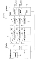
- the circuit characteristic measurement system 1 shown in FIG. 1 includes a signal voltage generation circuit 2, a measurement circuit 3, a control unit 4, a plurality of probe Pos for signal output, and a plurality of probe Pis for signal measurement.
- a plurality of circuits to be measured 51 to be measured are formed on, for example, one substrate 5.
- the circuit to be measured 51 may have, for example, a filter circuit, a circuit board, a transmission line, or other electrical characteristics.
- Each circuit to be measured 51 includes terminals T1 and T2.
- the plurality of circuits to be measured 51 may be one in which a plurality of the same circuits are integrated on one substrate 5 as a collective substrate, and different circuits 51 to be measured are formed on one substrate 5. It may be a thing. Further, the plurality of circuits to be measured 51 are not limited to the example formed on one substrate 5, and may be independent of each other.
- the signal voltage generation circuit 2 measures a plurality of periodic voltage signals having a predetermined reference frequency and a frequency m times (m is an integer) of the reference frequency according to the control signal from the control unit 4. It is sequentially applied to the measurement circuit 51.
- the signal voltage generation circuit 2 includes an oscillation circuit 21 and a clock buffer 22.
- Each periodic voltage signal is a signal including a frequency component of each fundamental wave and a higher-order frequency component which is a frequency component of two or more integral multiples of the fundamental wave.
- the oscillation circuit 21 outputs a periodic voltage signal having a frequency corresponding to the control signal from the control unit 4 to the clock buffer 22.
- a VCO Voltage Controlled Oscillator
- the frequency fluctuation range may be expanded by combining the oscillation circuit 21 with a frequency dividing circuit or the like.
- the clock buffer 22 is a signal output circuit that shapes the periodic voltage signal output from the oscillation circuit 21 into a square wave and distributes it to a plurality of probes Po for output. As a result, a rectangular wave periodic voltage signal is output from the signal voltage generation circuit 2.
- each probe Po When performing measurement, each probe Po is in contact with the terminal T1 of each circuit under test 51, and each probe Pi is in contact with the terminal T2 of each circuit 51 to be measured.
- the periodic voltage signal distributed and output from the clock buffer 22 is applied to the terminal T1 of each circuit under test 51 via each probe Po, passes through each circuit 51 to be measured, and is output to the terminal T2.
- the measuring circuit 3 sequentially measures the electric power of the signal generated in the measured circuit 51 by sequentially applying the periodic voltage signal to the measured circuit 51 according to the control signal from the control unit 4.
- various general-purpose ICs Integrated Circuits capable of measuring RMS power, such as the RMS power detector LTC5596 manufactured by Analog Devices, Inc., and the ADL5904 manufactured by Analog Devices, Inc., can be used.
- the measurement circuit 3 and the probe Pi are provided with the number of periodic voltage signals distributed and output from the clock buffer 22, that is, the same number as the probe Po.
- Each measurement circuit 3 acquires a signal from the terminal T2 of each circuit under test 51 via each probe Pi, and measures the effective value power thereof. Each measurement circuit 3 outputs a signal indicating the measured effective value power to the control unit 4.
- the circuit characteristic measurement system 1 includes the clock buffer 22 and the plurality of measurement circuits 3, so that the characteristics of the plurality of measured circuits 51 can be measured in parallel. As a result, the measurement time can be shortened.
- the circuit characteristic measurement system 1 does not necessarily have to include the clock buffer 22 and the plurality of measurement circuits 3. Instead of the clock buffer 22, a buffer circuit that shapes the waveform into a square wave may be provided, the measurement circuit 3 may be one, and the characteristics of the circuit to be measured 51 may be measured one by one.
- the control unit 4 is, for example, a CPU (Central Processing Unit) that executes a predetermined arithmetic process, a RAM (Random Access Memory) that temporarily stores data, a flash memory or an HDD (Hard Disk Drive) that stores a predetermined control program. ) And other non-volatile storage units 43, and peripheral circuits thereof and the like.
- a CPU Central Processing Unit
- RAM Random Access Memory
- HDD Hard Disk Drive
- the control unit 4 functions as the measurement control unit 41 and the transfer function calculation unit 42 by executing the control program stored in the storage unit 43, for example.
- the measurement control unit 41 outputs a control signal to the signal voltage generation circuit 2, and outputs a periodic voltage signal of a predetermined frequency from the signal voltage generation circuit 2. As a result, a periodic voltage signal having a predetermined frequency is applied to the terminal T1 of each circuit to be measured 51. Further, the measurement control unit 41 causes each measurement circuit 3 to measure the power of the signal output from the terminal T2 while the signal voltage generation circuit 2 is outputting the periodic voltage signal of a predetermined frequency.
- the measurement control unit 41 stores the electric power measured by each measurement circuit 3 in, for example, a storage unit 43 in association with the frequency output from the signal voltage generation circuit 2. After that, the measurement control unit 41 repeats the output of the periodic voltage signal by the signal voltage generation circuit 2 and the power measurement by each measurement circuit 3 while changing the frequency, and stores the measured power in association with the frequency. It is stored in the part 43 and the like.
- the transfer function calculation unit 42 calculates the transfer function of each circuit to be measured 51 based on a plurality of electric powers measured by each measurement circuit 3 using a preset mathematical formula.
- a preset mathematical expression for example, a mathematical expression obtained by expanding the periodic voltage signal into a Fourier series can be used.
- Formulas obtained by expanding the periodic voltage signal into a Fourier series include formulas (1), formulas (1)', formulas (2), formulas (2)', formulas (3), or formulas (3)', which will be described later. Can be used.
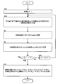
- the measurement control unit 41 initializes the variable m to 1 (step S1). Next, the measurement control unit 41 outputs a control signal to the signal voltage generation circuit 2 , outputs a periodic voltage signal of the reference frequency mf 0 from the signal voltage generation circuit 2, and applies the control signal to each circuit to be measured 51 (step S2). ).
- the electric power of the signal transmitted through each circuit to be measured 51 is measured as P (mf 0 ) in each measurement circuit 3, and a signal indicating the measured value is output to the control unit 4 (step S3).
- the measurement control unit 41 stores the signal power P (mf 0 ) obtained from each circuit to be measured 51 in the storage unit 43 or the like in association with the frequency mf 0 (step S4).
- the measurement control unit 41 compares the variable m with, for example, 7 (step S5).
- the variable m is less than 7 (NO in step S5), 2 is added to the variable m in order to change the frequency of the periodic voltage signal and continue the measurement (step S6), and steps S2 to S5 are repeated again.
- a periodic voltage signal having a reference frequency of 3f 0 is applied to each circuit to be measured (step S2), signal power P (3f 0 ) is measured in each measurement circuit 3 (step S3), and each circuit to be measured 51 is measured.
- the signal power P (3f 0 ) of the above is stored in association with the frequency 3f 0 (step S4).
- steps S2 to S6 are repeated until the variable m becomes, for example, 7 in step S5.
- the signal powers P (f 0 ), P (3f 0 ), P (5f 0 ), P (7f) of each circuit under test 51 are associated with the reference frequencies f 0 , 3f 0 , 5f 0 , 7f 0. 0 ) is stored in the storage unit 43 or the like.
- the transfer function calculation unit 42 determines P (f 0 ), P (3f 0 ), P (5f 0 ), P (7f 0 ) for each circuit 51 to be measured. Is substituted into the following equation (1)'to calculate the transfer functions H 2 (f 0 ), H 2 (3f 0 ), H 2 (5f 0 ), and H 2 (7f 0 ) of each circuit to be measured 51. (Step S7).
- B is the peak voltage of the periodic voltage signal (square wave) output from the signal voltage generation circuit 2
- A is the effective value power of the periodic voltage signal.
- the transfer function H 2 (f 0), H 2 (3f 0), H 2 (5f 0), H 2 (7f 0) since it represents the characteristic of the circuit under test 51, the transfer function H 2 (f 0 ), H 2 (3f 0 ), H 2 (5f 0 ), and H 2 (7f 0 ), the characteristics of the circuit to be measured 51 can be measured.
- the transfer functions H (f 0 ), H 2 (3f 0 ), H 2 (5f 0 ), and H 2 (7f 0 ) are obtained.
- H (5f 0 ), H (7f 0 ) may be calculated as the characteristics of the circuit.
- H is an amplitude transfer function and does not include phase information.
- the signal voltage generation circuit 2 shown in FIG. 1 outputs a rectangular wave voltage signal as a periodic voltage signal.
- the DC voltage may be switched by a switching element, and a periodic voltage signal can be easily generated by using a commercially available semiconductor element such as a clock buffer 22 or a buffer. Therefore, according to the circuit characteristic measurement system 1, the characteristic of the circuit under test 51 is measured by outputting the voltage signal of the square wave as a periodic voltage signal without using the current source circuit that controls the current through which the square wave current flows. Can be done.
- the clock buffer 22 distributes the periodic voltage signal to the plurality of measured circuits 51 and the plurality of measuring circuits 3 can measure the power of the signal transmitted through each of the measured circuits 51 in parallel at the same time, the measured voltage can be measured. It is easy to shorten the measurement time as compared with the case where the characteristics of the circuit 51 are sequentially measured one by one.
- frequency f 0 , 3f 0 , 5f 0 , 7f 0 periodic voltage signals are applied, and the signal powers P (f 0 ), P (3f 0 ), P (5f 0 ), P (7f 0 ).
- the frequency of the periodic voltage signal to be applied shall be 5 or more (f 0 , 3f 0 , 5f 0 , 7f 0 , 9f 0 , ...)
- the -1st power matrix in the equation (1) shall be 5 ⁇ 5 or more. , or five numbers of parameters transfer functions (H 2 (f 0), H 2 (3f 0), H 2 (5f 0), H 2 (7f 0), H 2 (9f 0) ⁇ ) as May be good.
- the number of parameters of the transfer function By increasing the number of parameters of the transfer function, it becomes possible to measure the circuit characteristics of the circuit under test 51 with higher accuracy. On the other hand, if the number of parameters of the transfer function is increased, the measurement takes time and the amount of arithmetic processing also increases. Therefore, the number of transfer function parameters to be appropriately calculated may be determined according to the balance between the required measurement accuracy of the circuit characteristics and the measurement time or the amount of arithmetic processing.
- the periodic voltage signal does not necessarily have to be a rectangular wave, and may be a periodic waveform that includes a high-order frequency component and changes periodically.
- a periodic waveform different from the rectangular wave is used as the periodic voltage signal, it is necessary to measure the characteristics of the circuit portion related to the measurement of the transfer function in the circuit characteristic measurement system 1 in advance.
- a spectrum analyzer 6 is used instead of the measurement circuit 3 when measuring the characteristics of the circuit portion related to the measurement of the transfer function.
- the periodic voltage signal output from the signal voltage generation circuit 2a is different from the signal voltage generation circuit 2a and the signal voltage generation circuit 2 in that the periodic voltage signal does not necessarily have to be a square wave.
- the periodic voltage signal output from the signal voltage generation circuit 2a may be a periodic waveform that changes periodically, and the signal waveform is not limited.
- the periodic voltage signal output from the signal voltage generation circuit 2a may be, for example, an asymmetric waveform signal having different rising slopes and falling slopes.
- the measurement control unit 41a is different from the measurement control unit 41 in that it further executes a process of measuring the characteristics of the circuit portion related to the measurement of the transfer function.
- the transfer function calculation unit 42a is different from the transfer function calculation unit 42 in that the transfer function of the measurement circuit 3 is calculated by using the equations (2)'and the equation (2) instead of the equations (1)' and (1). different.
- the characteristics of the pair of probes Po and Pi connected to the first circuit to be measured 51 are measured.
- the probe Pi connected to the first circuit to be measured 51 is connected to the spectrum analyzer 6, and the probe Po paired with the probe Pi is brought into contact with the probe Pi (step S11).
- the measurement control unit 41a initializes the variable m to 1 (step S12). m is a natural number (1, 2, 3, ). Next, the measurement control unit 41a outputs a control signal to the signal voltage generation circuit 2a, and outputs a periodic voltage signal of the reference frequency mf 0 from the signal voltage generation circuit 2a to the probe Po (step S13). Then, the periodic voltage signal is input to the spectrum analyzer 6 via the probes Po and Pi.
- the power A (mn) m when n is 3 or more is , The effective value power of the nth harmonic with respect to the fundamental wave having a frequency m times the reference frequency f 0.
- the crest value B (mn) m is the reference. represents the amplitude voltage of the n-th harmonic of the fundamental wave having m times the frequency of the frequency f 0.
- the number of m and the number of harmonics to be measured may be appropriately determined according to the required measurement accuracy of the circuit characteristics.
- the power A (mn) m measured in this way may be stored in the storage unit 43 by transmitting it from, for example, the spectrum analyzer 6 to the control unit 4, and for example, the power A (mn) m may be stored from the spectrum analyzer 6. It may be stored in a storage medium such as a memory card or a USB memory, and the storage medium may be stored in the storage unit 43 by being read by the control unit 4, or the storage medium may be used as it is as a part of the storage unit 43. ..
- the measurement control unit 41 compares the variable m with 7 (step S15). When the variable m is less than 7 (NO in step S15), 1 is added to the variable m in order to change the frequency of the periodic voltage signal and continue the measurement (step S16), and steps S13 to S15 are repeated again.
- the upper limit of m may be appropriately determined according to the required measurement accuracy of the circuit characteristics.
- steps S11 to S16 are sequentially performed for the remaining other probe Po and Pi pairs.
- the circuit characteristic measurement system 1a capable of measuring the characteristics of the measurement circuit 3 using a periodic voltage signal different from that of the square wave is shown in parentheses in FIG.
- the circuit characteristic measurement system 1a is different from the circuit characteristic measurement system 1 in that the signal voltage generation circuit 2a, the control unit 4a, the measurement control unit 41, and the transfer function calculation unit 42 are replaced with the signal voltage generation circuit 2a, the control unit 4a, and the measurement. It differs in that it includes a control unit 41a and a transfer function calculation unit 42a.
- the above-mentioned electric power A (mn) m is measured and stored in advance in the storage unit 43 of the control unit 4a.
- the measurement control unit 41a initializes the variable m to 1 (step S21). Next, the measurement control unit 41a outputs a control signal to the signal voltage generation circuit 2a , outputs a periodic voltage signal of the reference frequency mf 0 from the signal voltage generation circuit 2a, and applies the periodic voltage signal to each circuit under test 51 (step S22). ).
- the electric power of the signal transmitted through each circuit to be measured 51 is measured as P (mf 0 ) in each measurement circuit 3, and a signal indicating the measured value is output to the control unit 4a (step S3).
- the measurement control unit 41a stores the signal power P (mf 0 ) obtained from each circuit to be measured 51 in the storage unit 43 or the like in association with the frequency mf 0 (step S4).
- the measurement control unit 41a compares the variable m with, for example, 6 (step S23).
- the variable m is less than 6 (NO in step S23)
- 1 is added to the variable m in order to change the frequency of the periodic voltage signal and continue the measurement (step S24), and steps S22 to S23 are repeated again.
- Steps S22 ⁇ S24 by repeating in step S23 until the variable m is 6, as in step S1 ⁇ S6, in association with the reference frequency f 0 ⁇ 6f 0, the signal power P of each of the measuring circuit 51 (F 0 ) to P (6f 0 ) are stored in the storage unit 43 or the like.
- the transfer function calculation unit 42a substitutes P (f 0 ) to P (6f 0 ) into the following equation (2)'for each circuit 51 to be measured. based on the power a (mn) m which was previously stored in the storage unit 43 the transfer function of H 2 the measured circuit 51 (f 0) ⁇ H 2 (6f 0) is calculated (step S25).
- the transfer function H 2 (f 0) even when using different periodic voltage signal, representing the characteristics of each circuit to be measured 51 is a rectangular wave ⁇ H 2 (6f 0 ) Can be measured. Note that by determining the square root of the transfer function H 2 (f 0) ⁇ H 2 (6f 0), may be calculated transfer function H (f 0) ⁇ H a (6f 0) as a characteristic of the circuit.
- a periodic voltage signal of a rectangular wave can be applied to the circuit under test 51 depending on the performance of the clock buffer 22, the impedance of the probes Po and Pi, the floating capacitance of the circuit, and the like. Even if it is difficult, the characteristics of the circuit under test 51 can be measured.
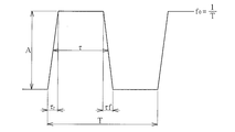
- the waveform becomes symmetric with respect to the symmetry axis C.
- a periodic voltage signal hereinafter, referred to as a symmetrical periodic voltage signal
- the periodic voltage signal shown in FIG. 7 is, for example, a trapezoidal wave having the same rising and falling slopes.
- the configurations of the signal voltage generation circuit 2b and the control unit 4b are different from those of the signal voltage generation circuit 2a and the control unit 4a.
- the signal voltage generation circuit 2b outputs a periodic voltage signal having a symmetrical waveform.
- the measurement control unit 41b differs from the measurement control unit 41a in the following points.
- step S14 the measurement control unit 41b does not measure the power A (mn) m at which the harmonic order n is an even number.
- step S16 the measurement control unit 41b does not measure the power A (mn) m in which m is an even number by adding 2 to m.
- the measurement control unit 41b uses the equation (3)'described later instead of the equation (2)'.
- the measurement control unit 41b initializes the variable m to 1 (step S31). Next, the measurement control unit 41b outputs a control signal to the signal voltage generation circuit 2b , outputs a periodic voltage signal of the reference frequency mf 0 from the signal voltage generation circuit 2b, and applies the periodic voltage signal to each circuit under test 51 (step S32). ).
- the electric power of the signal transmitted through each circuit to be measured 51 is measured as P (mf 0 ) in each measurement circuit 3, and a signal indicating the measured value is output to the control unit 4b (step S3).
- the measurement control unit 41b stores the signal power P (mf 0 ) obtained from each circuit to be measured 51 in the storage unit 43 or the like in association with the frequency mf 0 (step S4).
- the measurement control unit 41b compares the variable m with, for example, 7 (step S33).
- the variable m is less than 7 (NO in step S33)
- 2 is added to the variable m in order to change the frequency of the periodic voltage signal and continue the measurement (step S34), and steps S32 to S33 are repeated again.
- step S34 the periodic voltage signal having the reference frequency mf 0 with the even variable m is not output in step S32, and the signal power P (mf 0 ) with the even variable m is not measured in steps S3 and S4. I can't even remember.
- the reference frequencies f 0 , 3f 0 , 5f 0 , 7f 0 are associated with each other.
- the signal powers P (f 0 ), P (3f 0 ), P (5f 0 ), P (7f 0 ) of the circuit to be measured 51 are stored in the storage unit 43 or the like.
- the transfer function calculation unit 42b requests P (f 0 ), P (3f 0 ), P (5f 0 ), P (7f 0 ) for each circuit 51 to be measured.
- the following equation (3) is substituted into 'pre-stored so power a in the storage unit 43 the transfer function H 2 (f 0) of each of the measuring circuit 51 based on the (mn) m, H 2 ( 3f 0) , H 2 (5f 0 ), H 2 (7f 0 ) are calculated (step S35).
- H 2 (f 0 ), H 2 (3f 0 ), H 2 (5f 0 ), and H 2 (7f 0 ) the transfer functions H (f 0 ) and H (3f 0) are obtained.
- H (5f 0 ), H (7f 0 ) may be calculated as the characteristics of the circuit.
- step S31 to S35 when a periodic voltage signal having a symmetrical waveform is used, the transfer functions H 2 (f 0 ), H 2 (3f 0 ), and H 2 (5f 0 ) of each circuit to be measured 51 are used. , H 2 (7f 0 ) can be calculated. Further, in step S3, it is not necessary to measure the signal power P (mf 0 ) having an even number of m, and in the equation (3)'of step S35, the terms having an even order can be reduced. The processing can be simplified in comparison.
- the probe Pi is brought into contact with the terminal T2 and the power of the transmitted wave through which the periodic voltage signal has passed through the circuit under test 51 is measured by the measurement circuit 3. Indicated. However, the probe Pi may be brought into contact with the terminal T1 and the power of the reflected wave reflected by the periodic voltage signal in the circuit under test 51 may be measured by the measurement circuit 3. Even when measuring the reflected wave, the reflection characteristic by the measurement circuit 3, that is, the transfer function of the reflected wave is measured by the same processing as in steps S1 to S7, S11 to S16, S21 to S25, and S31 to S35. Can be done.
- the transfer function calculation units 42, 42a and 42b are not necessarily limited to the example in which the equations (1)', (2)' and (3)'are used in steps S7, S25 and S35.
- the transfer function calculation units 42, 42a, and 42b may execute the operations represented by the equations (1)', (2)', and (3)', for example, the equation (1)', (2)', (3)'. You may calculate the mathematical expression in which 1)', (2)', and (3)' are expanded.
- equations (1), (1)', (2), (2)', (3), and (3)' are equations obtained by expanding the periodic voltage signal into a Fourier series. ..
- the equations (1), (2), and (3) correspond to the simplified notations of the same equations as the equations (1)', (2)', and (3)'.
- the following formula (A) is a formula expressed by expanding the periodic voltage signal of the reference frequency f 0 by Fourier series
- the formula (B) is a formula expressed by expanding the periodic voltage signal of the reference frequency 2f 0 by Fourier series
- the formula (C) is a formula that represents a periodic voltage signal of the reference frequency 3f 0 by Fourier series expansion.
- B (1n) 1 represents the peak value of the n-th harmonic component when the reference frequency f 0,
- B (2n) 2 represents the peak value of the n-th harmonic component when the reference frequency 2f 0,
- V F1 (t), V F2 (t), V F3 (t) is the following formula (G), expressed by (H), (I) ..
- Equations (2) and (2)' are obtained by modifying the equation (M). Therefore, equations (2) and (2)'are none other than equations obtained by expanding the periodic voltage signal into a Fourier series.
- a trapezoidal wave in which the rising time ⁇ r of the signal and the falling time ⁇ f of the signal are equal is the periodic voltage.
- the periodic voltage signal is expressed by the following equation (N) when expanded by Fourier series.
- the harmonic component having an even multiple of the frequency f 0 can be deleted from the equation (M).
- Equations (3) and (3)' are obtained by transforming equation (O). Therefore, equations (3) and (3)'are none other than equations obtained by expanding the periodic voltage signal into a Fourier series.
- -It is known to be ⁇ 1 / (2n-1) ⁇ . Therefore, by substituting the peak value B (mn) m of the nth harmonic into the term of the power A (mn) m of the equations (3) and (3)'and transforming the equation, the equation (1), Equation (1)'is obtained. Therefore, equations (1) and (1)'are none other than equations obtained by expanding the periodic voltage signal into a Fourier series.
- the circuit characteristic measurement system sequentially applies a plurality of periodic voltage signals having a predetermined reference frequency and a frequency that is an integral multiple of the reference frequency to the circuit to be measured.
- the measurement is performed using a signal voltage generation circuit, a measurement circuit that sequentially measures the power of the signal generated in the circuit to be measured by sequentially applying the periodic voltage signal to the circuit to be measured, and a preset mathematical formula.
- the periodic voltage signal includes a high-order frequency component, including a transmission function calculation unit that calculates a transmission function of the circuit under test based on the power measured by the circuit.
- a plurality of periodic voltage signals having a predetermined reference frequency and a frequency that is an integral multiple of the reference frequency are sequentially applied to the circuit to be measured.
- the measurement circuit uses a signal voltage application step, a measurement step of measuring the power of the signal generated in the measurement circuit by applying the periodic voltage signal to the measurement circuit, and a preset mathematical formula.
- the periodic voltage signal includes a high-order frequency component, including a transmission function calculation step of calculating the transmission function of the circuit under test based on the plurality of electric powers measured in.
- a plurality of periodic voltage signals are sequentially applied to the circuit under test to be measured, the power generated by the signals is sequentially measured, and based on these powers, a preset mathematical formula is used.
- the transfer function of the circuit under test is calculated.
- the transmission function of the circuit under test is generated by generating a periodic voltage signal, which is a voltage signal that can be easily generated, without using a current source circuit that controls the current through which a rectangular wave current flows as in Non-Patent Document 1. That is, the characteristics of the circuit under test can be measured.
- the periodic voltage signal is a square wave, and when the reference frequency is f 0 , the frequencies of the plurality of periodic voltage signals are preferably an odd multiple of the reference frequency f 0.
- the transfer function calculation unit uses the following formula, which is the mathematical formula. It is preferable to calculate the transfer functions H 2 (f 0 ), H 2 (3f 0 ), H 2 (5f 0 ), ... Of the circuit under test by performing the calculation represented by (1). ..
- the frequency that is an integral multiple is mf 0 (m is an integer of 2 or more)
- the transmission function calculation unit is based on the power A (mn) m stored in the storage unit.
- the periodic voltage signal can be made into a waveform symmetric with respect to the symmetric axis by arranging a symmetric axis perpendicular to the time axis at one point on the time axis in the signal waveform for one cycle.
- the frequency that is an integral multiple is mf 0 (m is an odd number of 3 or more)
- the power A (mn) m (n) of the fundamental wave and its harmonics
- Further includes a storage unit that stores harmonic orders: n 1, 3, 5, ...) In advance, and the transmission function calculation unit is based on the power A (mn) m stored in the storage unit.
- the measuring circuit measures the electric power of the reflected wave whose periodic voltage signal is reflected by the circuit under test.
- the periodic voltage signal is not limited to the transmitted wave transmitted through the circuit under test, and the periodic voltage signal is also transmitted by the circuit under test by measuring the power of the reflected wave reflected by the circuit under test. It is easy to calculate the function, that is, the circuit characteristics.
- the circuit characteristic measurement system and the circuit characteristic measurement method having such a configuration can measure the characteristics of the circuit under test without using a current source circuit that controls a current through which a square wave current flows.
Landscapes
- Physics & Mathematics (AREA)
- General Physics & Mathematics (AREA)
- Measurement Of Resistance Or Impedance (AREA)
Priority Applications (2)
| Application Number | Priority Date | Filing Date | Title |
|---|---|---|---|
| JP2021548477A JP7613663B2 (ja) | 2019-09-27 | 2020-09-28 | 回路特性測定システム、及び回路特性測定方法 |
| CN202080067185.1A CN114502967B (zh) | 2019-09-27 | 2020-09-28 | 电路特性测定系统及电路特性测定方法 |
Applications Claiming Priority (2)
| Application Number | Priority Date | Filing Date | Title |
|---|---|---|---|
| JP2019-176576 | 2019-09-27 | ||
| JP2019176576 | 2019-09-27 |
Publications (1)
| Publication Number | Publication Date |
|---|---|
| WO2021060558A1 true WO2021060558A1 (ja) | 2021-04-01 |
Family
ID=75165281
Family Applications (1)
| Application Number | Title | Priority Date | Filing Date |
|---|---|---|---|
| PCT/JP2020/036634 Ceased WO2021060558A1 (ja) | 2019-09-27 | 2020-09-28 | 回路特性測定システム、及び回路特性測定方法 |
Country Status (3)
| Country | Link |
|---|---|
| JP (1) | JP7613663B2 (https=) |
| CN (1) | CN114502967B (https=) |
| WO (1) | WO2021060558A1 (https=) |
Cited By (2)
| Publication number | Priority date | Publication date | Assignee | Title |
|---|---|---|---|---|
| WO2023192226A3 (en) * | 2022-03-28 | 2023-11-23 | Communications Test Design, Inc. | Radio frequency detector for test chamber |
| JP7579016B2 (ja) | 2022-06-23 | 2024-11-07 | 歐姆佳科技股▲ふん▼有限公司 | 複数の無線周波数素子群試験装置及びその方法 |
Citations (7)
| Publication number | Priority date | Publication date | Assignee | Title |
|---|---|---|---|---|
| JPH08184624A (ja) * | 1994-12-28 | 1996-07-16 | Sony Corp | 伝達関数測定装置 |
| JPH09236627A (ja) * | 1995-12-27 | 1997-09-09 | Toshiba Corp | 自励システムの雑音解析装置 |
| US5794008A (en) * | 1996-02-28 | 1998-08-11 | Raytheon Company | Electrical network modeling tool and analyzer |
| JP2005536749A (ja) * | 2002-08-20 | 2005-12-02 | ザ ボード オブ リージェンツ,ザ ユニバーシティ オブ テキサス システム | 制御可能な減衰と伝播速度とを有する波形を伝送する方法 |
| JP2016223947A (ja) * | 2015-06-01 | 2016-12-28 | 三菱電機株式会社 | 位相余裕ゲイン余裕測定回路 |
| JP2018509620A (ja) * | 2015-03-13 | 2018-04-05 | ローズマウント インコーポレイテッド | 静電容量式センサの電極変位計測のための高分解能デルタシグマ変調器 |
| US20190064222A1 (en) * | 2017-08-30 | 2019-02-28 | Analog Devices Global Unlimited Company | Managing the determination of a transfer function of a measurement sensor |
Family Cites Families (9)
| Publication number | Priority date | Publication date | Assignee | Title |
|---|---|---|---|---|
| JPH05260662A (ja) * | 1992-03-10 | 1993-10-08 | Tokyo Electric Power Co Inc:The | アクティブフィルタを利用した電圧変動抑制装置 |
| JP3257220B2 (ja) * | 1994-01-12 | 2002-02-18 | 株式会社アドバンテスト | 伝達関数非接触測定装置 |
| JPH0894691A (ja) * | 1994-09-29 | 1996-04-12 | Meidensha Corp | 系統周波数特性の検出方法 |
| JP4769323B2 (ja) * | 2007-03-29 | 2011-09-07 | 旭化成株式会社 | 信号処理装置、エコーキャンセラ、信号処理方法 |
| JP5485618B2 (ja) * | 2009-08-26 | 2014-05-07 | パナソニック株式会社 | センサ装置 |
| JP5887110B2 (ja) * | 2011-11-21 | 2016-03-16 | 株式会社ダイヘン | 電力計測装置、インバータ制御回路、系統連系インバータシステム、および、電力計測方法 |
| JP2016133490A (ja) * | 2015-01-22 | 2016-07-25 | 日本電信電話株式会社 | 安定性判別装置 |
| CN105222950B (zh) * | 2015-09-18 | 2017-09-05 | 中国水利水电科学研究院 | 一种真假倍频压力脉动信号的区分方法 |
| US10459013B2 (en) * | 2016-06-17 | 2019-10-29 | Analog Devices Global | Apparatus for and method of providing measurements of uncertainty in respect of a transfer function |
-
2020
- 2020-09-28 WO PCT/JP2020/036634 patent/WO2021060558A1/ja not_active Ceased
- 2020-09-28 JP JP2021548477A patent/JP7613663B2/ja active Active
- 2020-09-28 CN CN202080067185.1A patent/CN114502967B/zh active Active
Patent Citations (7)
| Publication number | Priority date | Publication date | Assignee | Title |
|---|---|---|---|---|
| JPH08184624A (ja) * | 1994-12-28 | 1996-07-16 | Sony Corp | 伝達関数測定装置 |
| JPH09236627A (ja) * | 1995-12-27 | 1997-09-09 | Toshiba Corp | 自励システムの雑音解析装置 |
| US5794008A (en) * | 1996-02-28 | 1998-08-11 | Raytheon Company | Electrical network modeling tool and analyzer |
| JP2005536749A (ja) * | 2002-08-20 | 2005-12-02 | ザ ボード オブ リージェンツ,ザ ユニバーシティ オブ テキサス システム | 制御可能な減衰と伝播速度とを有する波形を伝送する方法 |
| JP2018509620A (ja) * | 2015-03-13 | 2018-04-05 | ローズマウント インコーポレイテッド | 静電容量式センサの電極変位計測のための高分解能デルタシグマ変調器 |
| JP2016223947A (ja) * | 2015-06-01 | 2016-12-28 | 三菱電機株式会社 | 位相余裕ゲイン余裕測定回路 |
| US20190064222A1 (en) * | 2017-08-30 | 2019-02-28 | Analog Devices Global Unlimited Company | Managing the determination of a transfer function of a measurement sensor |
Cited By (4)
| Publication number | Priority date | Publication date | Assignee | Title |
|---|---|---|---|---|
| WO2023192226A3 (en) * | 2022-03-28 | 2023-11-23 | Communications Test Design, Inc. | Radio frequency detector for test chamber |
| US12126391B2 (en) | 2022-03-28 | 2024-10-22 | Communications Test Design, Inc. | Radio frequency detector for test chamber |
| EP4500196A4 (en) * | 2022-03-28 | 2026-03-18 | Communications Test Design Inc | RADIOFREQUENCY DETECTOR FOR TEST CHAMBER |
| JP7579016B2 (ja) | 2022-06-23 | 2024-11-07 | 歐姆佳科技股▲ふん▼有限公司 | 複数の無線周波数素子群試験装置及びその方法 |
Also Published As
| Publication number | Publication date |
|---|---|
| CN114502967B (zh) | 2025-05-16 |
| JP7613663B2 (ja) | 2025-01-15 |
| JPWO2021060558A1 (https=) | 2021-04-01 |
| CN114502967A (zh) | 2022-05-13 |
Similar Documents
| Publication | Publication Date | Title |
|---|---|---|
| Amin et al. | Gravitational waves from asymmetric oscillon dynamics? | |
| JP4789272B2 (ja) | パワーインテグリティ解析装置、パワーインテグリティ解析方法及びプログラム | |
| US10914782B2 (en) | Test system and test method for testing a device under test | |
| WO2021060558A1 (ja) | 回路特性測定システム、及び回路特性測定方法 | |
| JP2009074941A (ja) | 周期信号の振幅測定方法および装置並びに磁気ヘッドの試験方法および装置 | |
| KR100269704B1 (ko) | 지연 소자 시험 장치 및 시험 기능을 갖는 집적 회로 | |
| JP3625400B2 (ja) | 可変遅延素子のテスト回路 | |
| Esposito et al. | Nonperturbative test of consistency relations and their violation | |
| Davidson et al. | Improved bandwidth and noise resilience in thermal impedance spectroscopy by mixing PRBS signals | |
| Chaberski et al. | Comparison of interpolators used for time-interval measurement systems based on multiple-tapped delay line | |
| EP3751238A1 (en) | Correction circuit and related signal processing circuit, and chip | |
| CN103069248B (zh) | 导体长测量装置以及导体长测量方法 | |
| JPWO2021060558A5 (https=) | ||
| CN203734620U (zh) | 一种基于忆阻器的Duffing-van der Pol 振荡电路 | |
| JP5274428B2 (ja) | 測定装置および試験装置 | |
| JP5407088B2 (ja) | 発振器の内部機構の推定方法、推定プログラム及び推定装置 | |
| Pejić et al. | A proposal of a novel method for generating discrete analog uniform noise | |
| CN111416659B (zh) | 一种光信号时域波形测量方法、装置、电子设备及介质 | |
| JPH11101851A (ja) | 遅延時間測定回路及び遅延時間測定方法 | |
| JP2000332584A (ja) | 遅延時間調整方法及び遅延時間調整回路 | |
| JP2014215048A (ja) | 電源装置およびそれを用いた試験装置 | |
| US12360152B2 (en) | Integrated current monitor using variable drain-to-source voltages | |
| JP6274638B2 (ja) | 周波数調整回路および周波数調整方法 | |
| US10013015B2 (en) | Fast auto-balancing AC bridge | |
| CN104764914A (zh) | 误差补偿方法与应用此方法的自动测试设备 |
Legal Events
| Date | Code | Title | Description |
|---|---|---|---|
| 121 | Ep: the epo has been informed by wipo that ep was designated in this application |
Ref document number: 20867621 Country of ref document: EP Kind code of ref document: A1 |
|
| ENP | Entry into the national phase |
Ref document number: 2021548477 Country of ref document: JP Kind code of ref document: A |
|
| NENP | Non-entry into the national phase |
Ref country code: DE |
|
| 122 | Ep: pct application non-entry in european phase |
Ref document number: 20867621 Country of ref document: EP Kind code of ref document: A1 |
|
| WWG | Wipo information: grant in national office |
Ref document number: 202080067185.1 Country of ref document: CN |