WO2021059914A1 - 電子回路装置 - Google Patents
電子回路装置 Download PDFInfo
- Publication number
- WO2021059914A1 WO2021059914A1 PCT/JP2020/033435 JP2020033435W WO2021059914A1 WO 2021059914 A1 WO2021059914 A1 WO 2021059914A1 JP 2020033435 W JP2020033435 W JP 2020033435W WO 2021059914 A1 WO2021059914 A1 WO 2021059914A1
- Authority
- WO
- WIPO (PCT)
- Prior art keywords
- electronic circuit
- heat
- circuit device
- metal layer
- wall portions
- Prior art date
- Legal status (The legal status is an assumption and is not a legal conclusion. Google has not performed a legal analysis and makes no representation as to the accuracy of the status listed.)
- Ceased
Links
Images






Classifications
-
- H—ELECTRICITY
- H10—SEMICONDUCTOR DEVICES; ELECTRIC SOLID-STATE DEVICES NOT OTHERWISE PROVIDED FOR
- H10W—GENERIC PACKAGES, INTERCONNECTIONS, CONNECTORS OR OTHER CONSTRUCTIONAL DETAILS OF DEVICES COVERED BY CLASS H10
- H10W40/00—Arrangements for thermal protection or thermal control
- H10W40/20—Arrangements for cooling
- H10W40/22—Arrangements for cooling characterised by their shape, e.g. having conical or cylindrical projections
- H10W40/226—Arrangements for cooling characterised by their shape, e.g. having conical or cylindrical projections characterised by projecting parts, e.g. fins to increase surface area
- H10W40/228—Arrangements for cooling characterised by their shape, e.g. having conical or cylindrical projections characterised by projecting parts, e.g. fins to increase surface area the projecting parts being wire-shaped or pin-shaped
-
- H—ELECTRICITY
- H10—SEMICONDUCTOR DEVICES; ELECTRIC SOLID-STATE DEVICES NOT OTHERWISE PROVIDED FOR
- H10W—GENERIC PACKAGES, INTERCONNECTIONS, CONNECTORS OR OTHER CONSTRUCTIONAL DETAILS OF DEVICES COVERED BY CLASS H10
- H10W40/00—Arrangements for thermal protection or thermal control
- H10W40/20—Arrangements for cooling
- H10W40/22—Arrangements for cooling characterised by their shape, e.g. having conical or cylindrical projections
-
- H—ELECTRICITY
- H10—SEMICONDUCTOR DEVICES; ELECTRIC SOLID-STATE DEVICES NOT OTHERWISE PROVIDED FOR
- H10W—GENERIC PACKAGES, INTERCONNECTIONS, CONNECTORS OR OTHER CONSTRUCTIONAL DETAILS OF DEVICES COVERED BY CLASS H10
- H10W70/00—Package substrates; Interposers; Redistribution layers [RDL]
- H10W70/60—Insulating or insulated package substrates; Interposers; Redistribution layers
- H10W70/611—Insulating or insulated package substrates; Interposers; Redistribution layers for connecting multiple chips together
-
- H—ELECTRICITY
- H10—SEMICONDUCTOR DEVICES; ELECTRIC SOLID-STATE DEVICES NOT OTHERWISE PROVIDED FOR
- H10W—GENERIC PACKAGES, INTERCONNECTIONS, CONNECTORS OR OTHER CONSTRUCTIONAL DETAILS OF DEVICES COVERED BY CLASS H10
- H10W70/00—Package substrates; Interposers; Redistribution layers [RDL]
- H10W70/60—Insulating or insulated package substrates; Interposers; Redistribution layers
- H10W70/62—Insulating or insulated package substrates; Interposers; Redistribution layers characterised by their interconnections
- H10W70/63—Vias, e.g. via plugs
- H10W70/635—Through-vias
-
- H—ELECTRICITY
- H10—SEMICONDUCTOR DEVICES; ELECTRIC SOLID-STATE DEVICES NOT OTHERWISE PROVIDED FOR
- H10W—GENERIC PACKAGES, INTERCONNECTIONS, CONNECTORS OR OTHER CONSTRUCTIONAL DETAILS OF DEVICES COVERED BY CLASS H10
- H10W70/00—Package substrates; Interposers; Redistribution layers [RDL]
- H10W70/60—Insulating or insulated package substrates; Interposers; Redistribution layers
- H10W70/67—Insulating or insulated package substrates; Interposers; Redistribution layers characterised by their insulating layers or insulating parts
- H10W70/68—Shapes or dispositions thereof
- H10W70/685—Shapes or dispositions thereof comprising multiple insulating layers
-
- H—ELECTRICITY
- H10—SEMICONDUCTOR DEVICES; ELECTRIC SOLID-STATE DEVICES NOT OTHERWISE PROVIDED FOR
- H10W—GENERIC PACKAGES, INTERCONNECTIONS, CONNECTORS OR OTHER CONSTRUCTIONAL DETAILS OF DEVICES COVERED BY CLASS H10
- H10W40/00—Arrangements for thermal protection or thermal control
- H10W40/60—Securing means for detachable heating or cooling arrangements, e.g. clamps
- H10W40/611—Bolts or screws
Definitions
- the present invention relates to an electronic circuit device in which heat-generating components such as semiconductor switching elements are mounted on a circuit board.
- the heat of the heat-generating components is transferred to a casing or the like that serves as a heat sink in some way.
- a structure that dissipates heat is required.
- a gel-like fluid heat transfer is performed between a circuit board on which a heat generating component is mounted and a member on the other side that receives heat, for example, a casing. It is known to intervene with materials. Since this type of fluid heat transfer material can follow and come into close contact with each facing surface, that is, the heat transfer surface, heat transfer is improved as compared with the case where there are minute gaps due to minute irregularities at the interface.
- An object of the present invention is to provide an electronic circuit device capable of easily dissipating heat from heat generating parts without using a fluid heat transfer material.
- the electronic circuit device includes a circuit board on which a heat generating component is mounted and having a through hole penetrating in the thickness direction, and a metal radiator having a boss portion inserted into the through hole. , Is provided.
- heat can be easily dissipated from heat generating parts without using a fluid heat transfer material.
- FIG. 1 An enlarged view of part A in FIG. FIG. 1 is an enlarged view of part B in FIG.
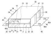
- the perspective view of the housing which accommodates the electronic circuit apparatus which concerns on this embodiment.
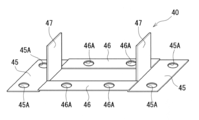
- the perspective view of the bracket which connects the electronic circuit apparatus which concerns on this embodiment to a vehicle body.
- FIG. 3 is a perspective view of a state in which the electronic circuit device according to the present embodiment is housed in a housing.
- FIG. 5 is a cross-sectional view showing a state in which the electronic circuit device according to the present embodiment is connected to a vehicle body via a bracket.
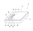
- the electronic circuit device 1 As shown in FIGS. 1 to 5, the electronic circuit device 1 according to the present embodiment is configured such that a circuit board 2 is placed on a metal radiator body 3 serving as a heat sink. A plurality of semiconductor switching elements (for example, MOS-FETs) 10 which are heat generating elements are surface-mounted on the circuit board 2.
- the circuit board 2 includes, for example, first to fourth conductive metal layers 4A, 4B, 4C, and 4D made of four layers of copper foil, and first to first glass epoxy resins and the like. It is composed of a multilayer substrate in which three resin layers 5A, 5B, and 5C are alternately arranged. Land portions and circuit wirings (patterns) necessary for mounting electronic components are appropriately formed on the first to fourth conductive metal layers 4A to 4D.
- the semiconductor switching element 10 which is a heat generating component (heating element) is electrically mounted with a lead terminal connected to a land portion (not shown) formed on the first conductive metal layer 4A of the circuit board 2.
- a heat receiving metal portion 8 is formed in a region of the first conductive metal layer 4A where the semiconductor switching element 10 is in contact so as to avoid circuit wiring (pattern) and the like. With reference to FIG. 3, in this region, the heat receiving metal portion 8 of the first conductive metal layer 4A, the first resin layer 5A, the second conductive metal layer 4B, the second resin layer 5B, the third conductive metal layer 4C, A plurality of first through holes 11 penetrating the third resin layer 5C and the fourth conductive metal layer 4D are formed.
- a metal layer 12 is provided on the inner peripheral surface of these first through holes 11 by electroplating or the like.
- a pattern is formed so as to hollow out around the first through hole 11 and is insulated from the first through hole 11.
- Each of the first through holes 11 having the metal layer 12 is provided to guide the heat from the semiconductor switching element 10 from the heat receiving metal portion 8 of the first conductive metal layer 4A to the third conductive metal layer 4C.
- each first through hole 11 serves as a heat transfer path from the semiconductor switching element 10 in the thickness direction of the circuit board 2.
- a plurality of second through holes 14 penetrating the circuit board 2 are formed in the vicinity of the semiconductor switching element 10. Specifically, the second through holes 14 penetrating the first to fourth conductive metal layers 4A to 4D and the first to third resin layers 5A to 5C constituting the circuit board 2 are formed. A metal layer 15 by electroplating or the like is provided on the inner peripheral surface of the second through hole 14. The first to third conductive metal layers 4A to 4C and the metal layer 15 of the second through hole 14 are insulated by interposing a resin layer 17, respectively. As a result, the second through hole 14 is insulated from the conductor portion of the semiconductor switching element 10.
- the fourth conductive metal layer 4D and the metal layer 15 of the second through hole 14 are connected by a pattern of the fourth conductive metal layer 4D. As described above, the fourth conductive metal layer 4D is insulated from the third conductive metal layer 4C by interposing the third resin layer 5C.
- the heat radiating body 3 is formed of a metal member such as an aluminum alloy having excellent heat conduction.
- the heat radiating body 3 includes a rectangular parallelepiped portion 20 and a plurality of boss portions 21 projecting from one surface of the rectangular parallelepiped portion 20.
- Each boss portion 21 has a columnar shape and is press-fitted into each of the second through holes 14 provided in the circuit board 2.
- the surface of the rectangular parallelepiped portion 20 facing the fourth conductive metal layer 4D of the circuit board 2 is formed in a substantially flat shape without unevenness.
- the rectangular parallelepiped portion 20 is configured to be in contact with the fourth conductive metal layer 4D of the circuit board 2 over substantially the entire area.
- the height of each boss portion 21 substantially matches the thickness of the circuit board 2.
- Each boss portion 21 is integrally connected to the rectangular parallelepiped portion 20 by press-fitting into one surface of the rectangular parallelepiped portion 20. Further, on the other surface of the rectangular parallelepiped portion 20 of the heat radiating body 3, a plurality of screw holes 24, 24 for fixing the electronic circuit device 1 to the bracket 40, which will be described later, are formed at intervals.
- the heat from the semiconductor switching element 10 is transferred from the heat receiving metal portion 8 of the first conductive metal layer 4A to the third conductive metal layer 12 of each first through hole 11. It is guided to the metal layer 4C. At this time, since the heat receiving metal layer 8 and the third conductive metal layer 4C are connected by the metal layer 12 of each first through hole 11, the heat transfer property is improved. Next, the heat of the third conductive metal layer 4C is guided to the fourth conductive metal layer 4D via the insulated third resin layer 5C.
- the third resin layer 5C is thin (the length in the thickness direction is short), and the third conductive metal layer 4C and the fourth conductive metal layer 4D are in contact with each other in a planar manner via the third resin layer 5C.
- the heat transfer property is good.
- the heat of the fourth conductive metal layer 4D is guided to the metal layer 15 of the second through hole 14 via the connected pattern, and from the metal layer 15, the heat radiator 3 is press-fitted (press-fitted). It is guided to the rectangular parallelepiped portion 20 via the boss portion 21 (in close contact) and dissipates heat.
- the fourth conductive metal layer 4D and the metal layer 15 of the second through hole 14 are connected to each other by metals, and the metal layer 15 and the boss portion 21 are in surface contact with each other.
- the heat transfer property is good because it is in close contact with the surface.
- the facing surface of the rectangular parallelepiped portion 20 is formed between the fourth conductive metal layer 4D and the rectangular parallelepiped portion 20 of the heat radiating body 3 in a substantially flat shape without unevenness, the circuit board 2 is warped. Since there are some parts where minute voids appear and are not in close contact with each other due to such factors, a good heat transfer effect cannot be expected.
- the electronic circuit device 1 is mounted in the housing 30.
- the housing 30 is made of synthetic resin and integrally molded.
- the housing 30 is formed in a substantially square tube shape so as to surround the electronic circuit device 1.
- the housing 30 has a pair of side wall portions 31 and 31 facing each other and a pair of support wall portions 32 and 32 that support the electronic circuit device 1 from the radiator 3 side (in FIG. 7, one of the front support wall portions 32 and 32). 32 is shown), and a covering wall portion 33 that faces the pair of support wall portions 32, 32 and covers the electronic circuit device 1 from each semiconductor switching element 10 side.
- a pair of engaging wall portions 34, 34 are projected outward from the outer surfaces of the pair of side wall portions 31, 31.
- the pair of engaging wall portions 34, 34 extend along the thickness direction of the electronic circuit device 1.
- stopper wall portions 35, 35 extend along the longitudinal direction of the housing 30. The distance between the pair of stopper wall portions 35, 35 and the pair of support wall portions 32, 32 is substantially the same as the thickness of the electronic circuit device 1.
- the housing 30 is connected to the vehicle body 43 by the bracket 40.
- the bracket 40 is made of metal.
- the bracket 40 is provided between the pair of vehicle body side fixed wall portions 45, 45 fixed to the vehicle body 43 side and the pair of vehicle body side fixed wall portions 45, 45, and is provided on the electronic circuit device 1 side.
- Mounting holes 45A and 45A are formed in the vehicle body side fixed wall portion 45 at intervals along the longitudinal direction thereof, respectively.
- Mounting holes 46A and 46A are formed in the circuit-side fixed wall portion 46 at intervals along the longitudinal direction thereof.
- the bracket 40 is connected to the housing 30 by engaging the housing-side engaging wall portions 47, 47 between the pair of engaging wall portions 34, 34 of the housing 30. Will be done.
- a pair of circuit-side fixed wall portions 46, 46 of the bracket 40 are arranged, respectively, a surface of the housing 30 on the covering wall portion 33 side of the pair of support wall portions 32, 32, and a pair of circuit-side fixed wall portions of the bracket 40.
- the surfaces of 46 and 46 on the side of the covering wall portion 33 are located on the same plane.
- the pair of vehicle body side fixed wall portions 45, 45 of the bracket 40 are located outside the pair of side wall portions 31, 31 of the housing 30.
- the electronic circuit device 1 is provided with a pair of support wall portions 32, 32 (a pair of circuit-side fixed wall portions 46, 46 of the bracket 40) and a pair of stopper wall portions 35 of the housing 30. , 35 and so as to be inserted.
- the heat radiating body 3 of the electronic circuit device 1 comes into contact with the pair of support wall portions 32, 32 of the housing 30, and also comes into contact with the pair of circuit-side fixed wall portions 46, 46 of the bracket 40.
- metal mounting screws 50, 50 are inserted into the mounting holes 46A, 46A provided in the pair of circuit-side fixed wall portions 46, 46 of the bracket 40, and the mounting screws are inserted. 50, 50 are screwed into the screw holes 24, 24 of the radiator body 3 of the electronic circuit device 1.
- the bracket 40 can be fixed to the electronic circuit device 1.
- metal mounting screws 51 and 51 are inserted into the mounting holes 45A and 45A provided in the pair of vehicle body side fixed wall portions 45 and 45 of the bracket 40, and the mounting screws are inserted. 51 and 51 are screwed into the screw holes 60 and 60 provided on the vehicle body 43 side.
- the bracket 40 can be fixed to the vehicle body 43.
- the electronic circuit device 1 including the housing 30 can be connected to the vehicle body 43 via the bracket 40.
- the heat from each semiconductor switching element 10 of the electronic circuit device 1 is guided to the heat radiating body 3 as described above, and finally, the heat from the heat radiating body 3 is transferred to each mounting screw 50, the bracket 40, and each mounting. It is guided to the vehicle body 43 via the screw 51.
- the semiconductor switching element 10 which is a heat generating component (heating element) is mounted, and the circuit board 2 has a second through hole 14 penetrating in the thickness direction.
- a metal radiator 3 having a boss portion 21 inserted into the second through hole 14 is provided.
- the heat from the semiconductor switching element 10 can be guided to the radiator 3 via the circuit board 2.
- heat can be easily dissipated from the semiconductor switching element 10 which is a heat generating component (heat generating element) without using a conventional fluid heat transfer material.
- the semiconductor switching element 10 which is a heat generating component (heating element) is used. Heat can be easily directed to the radiator 3. Further, in the electronic circuit device 1 according to the present embodiment, since the heat radiating body 3 of the electronic circuit device 1 is connected to the vehicle body 43 side via the metal bracket 40, heat from the heat radiating body 3 can be easily obtained. It can be guided to the vehicle body 43 side.
- the first aspect is a circuit board (2) on which a heat generating component (10) is mounted and having a through hole (14) penetrating in the thickness direction, and a boss portion (21) inserted into the through hole (14).
- the metal radiator (3) having the above-mentioned is provided.
- the circuit board (2) is configured by providing the through hole (14) in the vicinity of the heat generating component (10).
- the through hole (14) is insulated from the conductor portion of the heat generating component (10).
- the heat radiating body (3) is connected to the vehicle body (43) via a metal bracket (40).
- the heat generating component (10) is a heat generating element.
- the present invention is not limited to the above-described embodiment, and includes various modifications.
- the above-described embodiment has been described in detail in order to explain the present invention in an easy-to-understand manner, and is not necessarily limited to the one including all the described configurations.
- it is possible to replace a part of the configuration of one embodiment with the configuration of another embodiment and it is also possible to add the configuration of another embodiment to the configuration of one embodiment.
Landscapes
- Cooling Or The Like Of Electrical Apparatus (AREA)
- Cooling Or The Like Of Semiconductors Or Solid State Devices (AREA)
Priority Applications (2)
| Application Number | Priority Date | Filing Date | Title |
|---|---|---|---|
| DE112020004544.7T DE112020004544T5 (de) | 2019-09-25 | 2020-09-03 | Elektronische Schaltungsvorrichtung |
| JP2021548740A JPWO2021059914A1 (https=) | 2019-09-25 | 2020-09-03 |
Applications Claiming Priority (2)
| Application Number | Priority Date | Filing Date | Title |
|---|---|---|---|
| JP2019-174323 | 2019-09-25 | ||
| JP2019174323 | 2019-09-25 |
Publications (1)
| Publication Number | Publication Date |
|---|---|
| WO2021059914A1 true WO2021059914A1 (ja) | 2021-04-01 |
Family
ID=75166596
Family Applications (1)
| Application Number | Title | Priority Date | Filing Date |
|---|---|---|---|
| PCT/JP2020/033435 Ceased WO2021059914A1 (ja) | 2019-09-25 | 2020-09-03 | 電子回路装置 |
Country Status (3)
| Country | Link |
|---|---|
| JP (1) | JPWO2021059914A1 (https=) |
| DE (1) | DE112020004544T5 (https=) |
| WO (1) | WO2021059914A1 (https=) |
Citations (5)
| Publication number | Priority date | Publication date | Assignee | Title |
|---|---|---|---|---|
| JPS61134039U (https=) * | 1986-01-16 | 1986-08-21 | ||
| JPH08222671A (ja) * | 1994-12-14 | 1996-08-30 | Toshiba Corp | 回路モジュールの冷却装置 |
| JP2002344177A (ja) * | 2001-05-17 | 2002-11-29 | Denso Corp | 電子装置 |
| JP2010245174A (ja) * | 2009-04-02 | 2010-10-28 | Denso Corp | 電子制御ユニット及びその製造方法 |
| WO2014046004A1 (ja) * | 2012-09-21 | 2014-03-27 | 日立オートモティブシステムズ株式会社 | 電子制御装置 |
Family Cites Families (4)
| Publication number | Priority date | Publication date | Assignee | Title |
|---|---|---|---|---|
| JP2015047031A (ja) * | 2013-08-29 | 2015-03-12 | 株式会社オートネットワーク技術研究所 | 回路構成体 |
| JP6208072B2 (ja) | 2014-04-28 | 2017-10-04 | 日立オートモティブシステムズ株式会社 | 電子回路装置およびその製造方法 |
| JP6894816B2 (ja) * | 2017-09-28 | 2021-06-30 | 日本シイエムケイ株式会社 | 放熱金属片素材を用いたプリント配線板の製造方法 |
| JP7191312B2 (ja) | 2018-03-29 | 2022-12-19 | シヤチハタ株式会社 | 識別タグ、その干渉波形検出方法及びその真贋判定方法 |
-
2020
- 2020-09-03 JP JP2021548740A patent/JPWO2021059914A1/ja active Pending
- 2020-09-03 DE DE112020004544.7T patent/DE112020004544T5/de not_active Withdrawn
- 2020-09-03 WO PCT/JP2020/033435 patent/WO2021059914A1/ja not_active Ceased
Patent Citations (5)
| Publication number | Priority date | Publication date | Assignee | Title |
|---|---|---|---|---|
| JPS61134039U (https=) * | 1986-01-16 | 1986-08-21 | ||
| JPH08222671A (ja) * | 1994-12-14 | 1996-08-30 | Toshiba Corp | 回路モジュールの冷却装置 |
| JP2002344177A (ja) * | 2001-05-17 | 2002-11-29 | Denso Corp | 電子装置 |
| JP2010245174A (ja) * | 2009-04-02 | 2010-10-28 | Denso Corp | 電子制御ユニット及びその製造方法 |
| WO2014046004A1 (ja) * | 2012-09-21 | 2014-03-27 | 日立オートモティブシステムズ株式会社 | 電子制御装置 |
Also Published As
| Publication number | Publication date |
|---|---|
| DE112020004544T5 (de) | 2022-06-09 |
| JPWO2021059914A1 (https=) | 2021-04-01 |
Similar Documents
| Publication | Publication Date | Title |
|---|---|---|
| WO2016114099A1 (ja) | 回路構成体及び電気接続箱 | |
| WO2020017582A1 (ja) | モジュール | |
| WO2014203521A1 (ja) | 電子装置 | |
| JP6790902B2 (ja) | 電子装置 | |
| JP2014220921A (ja) | コネクタ一体型電子制御装置 | |
| JP5068098B2 (ja) | 放熱装置 | |
| JPH04113695A (ja) | 電子機器の放熱構造 | |
| JP2002171087A (ja) | 電子機器 | |
| JP6652144B2 (ja) | 電子部品、電子部品の製造方法、機構部品 | |
| WO2021059914A1 (ja) | 電子回路装置 | |
| JP2013254925A (ja) | 電子回路装置 | |
| JP3104749B2 (ja) | 回路装置及びその製造方法 | |
| CN116235297B (zh) | 基板单元 | |
| WO2020162614A1 (ja) | モジュール | |
| JP6200693B2 (ja) | 電子制御装置 | |
| JP2016076622A (ja) | 回路基板および電子装置 | |
| JP2006286757A (ja) | 電子機器の放熱構造 | |
| JP2019075415A (ja) | 半導体装置 | |
| JP6458688B2 (ja) | 電子装置 | |
| JP6633151B2 (ja) | 回路モジュール | |
| JP5072522B2 (ja) | 接続構造 | |
| JP6551566B1 (ja) | 電子部品の放熱構造 | |
| JP2018074058A (ja) | 電子装置 | |
| JP2019216160A (ja) | 電子制御装置 | |
| WO2021070569A1 (ja) | 電子機器 |
Legal Events
| Date | Code | Title | Description |
|---|---|---|---|
| 121 | Ep: the epo has been informed by wipo that ep was designated in this application |
Ref document number: 20868907 Country of ref document: EP Kind code of ref document: A1 |
|
| ENP | Entry into the national phase |
Ref document number: 2021548740 Country of ref document: JP Kind code of ref document: A |
|
| 122 | Ep: pct application non-entry in european phase |
Ref document number: 20868907 Country of ref document: EP Kind code of ref document: A1 |