WO2021044890A1 - 多層反射膜付き基板、反射型マスクブランク及び反射型マスク、並びに半導体装置の製造方法 - Google Patents
多層反射膜付き基板、反射型マスクブランク及び反射型マスク、並びに半導体装置の製造方法 Download PDFInfo
- Publication number
- WO2021044890A1 WO2021044890A1 PCT/JP2020/031888 JP2020031888W WO2021044890A1 WO 2021044890 A1 WO2021044890 A1 WO 2021044890A1 JP 2020031888 W JP2020031888 W JP 2020031888W WO 2021044890 A1 WO2021044890 A1 WO 2021044890A1
- Authority
- WO
- WIPO (PCT)
- Prior art keywords
- film
- substrate
- thin film
- multilayer reflective
- absorber
- Prior art date
- Legal status (The legal status is an assumption and is not a legal conclusion. Google has not performed a legal analysis and makes no representation as to the accuracy of the status listed.)
- Ceased
Links
Images


Classifications
-
- G—PHYSICS
- G03—PHOTOGRAPHY; CINEMATOGRAPHY; ANALOGOUS TECHNIQUES USING WAVES OTHER THAN OPTICAL WAVES; ELECTROGRAPHY; HOLOGRAPHY
- G03F—PHOTOMECHANICAL PRODUCTION OF TEXTURED OR PATTERNED SURFACES, e.g. FOR PRINTING, FOR PROCESSING OF SEMICONDUCTOR DEVICES; MATERIALS THEREFOR; ORIGINALS THEREFOR; APPARATUS SPECIALLY ADAPTED THEREFOR
- G03F1/00—Originals for photomechanical production of textured or patterned surfaces, e.g., masks, photo-masks, reticles; Mask blanks or pellicles therefor; Containers specially adapted therefor; Preparation thereof
- G03F1/22—Masks or mask blanks for imaging by radiation of 100nm or shorter wavelength, e.g. X-ray masks, extreme ultraviolet [EUV] masks; Preparation thereof
- G03F1/24—Reflection masks; Preparation thereof
-
- C—CHEMISTRY; METALLURGY
- C23—COATING METALLIC MATERIAL; COATING MATERIAL WITH METALLIC MATERIAL; CHEMICAL SURFACE TREATMENT; DIFFUSION TREATMENT OF METALLIC MATERIAL; COATING BY VACUUM EVAPORATION, BY SPUTTERING, BY ION IMPLANTATION OR BY CHEMICAL VAPOUR DEPOSITION, IN GENERAL; INHIBITING CORROSION OF METALLIC MATERIAL OR INCRUSTATION IN GENERAL
- C23C—COATING METALLIC MATERIAL; COATING MATERIAL WITH METALLIC MATERIAL; SURFACE TREATMENT OF METALLIC MATERIAL BY DIFFUSION INTO THE SURFACE, BY CHEMICAL CONVERSION OR SUBSTITUTION; COATING BY VACUUM EVAPORATION, BY SPUTTERING, BY ION IMPLANTATION OR BY CHEMICAL VAPOUR DEPOSITION, IN GENERAL
- C23C14/00—Coating by vacuum evaporation, by sputtering or by ion implantation of the coating forming material
- C23C14/06—Coating by vacuum evaporation, by sputtering or by ion implantation of the coating forming material characterised by the coating material
- C23C14/14—Metallic material, boron or silicon
-
- G—PHYSICS
- G03—PHOTOGRAPHY; CINEMATOGRAPHY; ANALOGOUS TECHNIQUES USING WAVES OTHER THAN OPTICAL WAVES; ELECTROGRAPHY; HOLOGRAPHY
- G03F—PHOTOMECHANICAL PRODUCTION OF TEXTURED OR PATTERNED SURFACES, e.g. FOR PRINTING, FOR PROCESSING OF SEMICONDUCTOR DEVICES; MATERIALS THEREFOR; ORIGINALS THEREFOR; APPARATUS SPECIALLY ADAPTED THEREFOR
- G03F1/00—Originals for photomechanical production of textured or patterned surfaces, e.g., masks, photo-masks, reticles; Mask blanks or pellicles therefor; Containers specially adapted therefor; Preparation thereof
- G03F1/38—Masks having auxiliary features, e.g. special coatings or marks for alignment or testing; Preparation thereof
- G03F1/48—Protective coatings
-
- G—PHYSICS
- G03—PHOTOGRAPHY; CINEMATOGRAPHY; ANALOGOUS TECHNIQUES USING WAVES OTHER THAN OPTICAL WAVES; ELECTROGRAPHY; HOLOGRAPHY
- G03F—PHOTOMECHANICAL PRODUCTION OF TEXTURED OR PATTERNED SURFACES, e.g. FOR PRINTING, FOR PROCESSING OF SEMICONDUCTOR DEVICES; MATERIALS THEREFOR; ORIGINALS THEREFOR; APPARATUS SPECIALLY ADAPTED THEREFOR
- G03F1/00—Originals for photomechanical production of textured or patterned surfaces, e.g., masks, photo-masks, reticles; Mask blanks or pellicles therefor; Containers specially adapted therefor; Preparation thereof
- G03F1/54—Absorbers, e.g. of opaque materials
-
- G—PHYSICS
- G03—PHOTOGRAPHY; CINEMATOGRAPHY; ANALOGOUS TECHNIQUES USING WAVES OTHER THAN OPTICAL WAVES; ELECTROGRAPHY; HOLOGRAPHY
- G03F—PHOTOMECHANICAL PRODUCTION OF TEXTURED OR PATTERNED SURFACES, e.g. FOR PRINTING, FOR PROCESSING OF SEMICONDUCTOR DEVICES; MATERIALS THEREFOR; ORIGINALS THEREFOR; APPARATUS SPECIALLY ADAPTED THEREFOR
- G03F7/00—Photomechanical, e.g. photolithographic, production of textured or patterned surfaces, e.g. printing surfaces; Materials therefor, e.g. comprising photoresists; Apparatus specially adapted therefor
- G03F7/20—Exposure; Apparatus therefor
-
- H—ELECTRICITY
- H01—ELECTRIC ELEMENTS
- H01L—SEMICONDUCTOR DEVICES NOT COVERED BY CLASS H10
- H01L21/00—Processes or apparatus adapted for the manufacture or treatment of semiconductor or solid state devices or of parts thereof
- H01L21/02—Manufacture or treatment of semiconductor devices or of parts thereof
- H01L21/027—Making masks on semiconductor bodies for further photolithographic processing not provided for in group H01L21/18 or H01L21/34
- H01L21/0271—Making masks on semiconductor bodies for further photolithographic processing not provided for in group H01L21/18 or H01L21/34 comprising organic layers
- H01L21/0273—Making masks on semiconductor bodies for further photolithographic processing not provided for in group H01L21/18 or H01L21/34 comprising organic layers characterised by the treatment of photoresist layers
- H01L21/0274—Photolithographic processes
-
- H—ELECTRICITY
- H01—ELECTRIC ELEMENTS
- H01J—ELECTRIC DISCHARGE TUBES OR DISCHARGE LAMPS
- H01J49/00—Particle spectrometers or separator tubes
- H01J49/02—Details
- H01J49/10—Ion sources; Ion guns
- H01J49/14—Ion sources; Ion guns using particle bombardment, e.g. ionisation chambers
- H01J49/142—Ion sources; Ion guns using particle bombardment, e.g. ionisation chambers using a solid target which is not previously vapourised
-
- H—ELECTRICITY
- H01—ELECTRIC ELEMENTS
- H01J—ELECTRIC DISCHARGE TUBES OR DISCHARGE LAMPS
- H01J49/00—Particle spectrometers or separator tubes
- H01J49/26—Mass spectrometers or separator tubes
- H01J49/34—Dynamic spectrometers
- H01J49/40—Time-of-flight spectrometers
Definitions
- the present invention relates to a reflective mask used for manufacturing a semiconductor device, a substrate with a multilayer reflective film used for manufacturing a reflective mask, and a reflective mask blank.
- the present invention also relates to a method for manufacturing a semiconductor device using the reflective mask.
- EUV lithography which is an exposure technique using extreme ultraviolet (hereinafter referred to as "EUV") light
- EUV light refers to light in the wavelength band of the soft X-ray region or the vacuum ultraviolet region, and specifically, light having a wavelength of about 0.2 to 100 nm.
- a reflective mask has been proposed as a transfer mask used in EUV lithography.
- the reflective mask is an absorber which is a multilayer reflective film formed on a substrate for reflecting exposure light and a patterned absorber film formed on the multilayer reflective film for absorbing exposure light. It has a membrane pattern.
- the reflective mask is manufactured from a reflective mask blank having a substrate, a multilayer reflective film formed on the substrate, and an absorber film formed on the multilayer reflective film.
- the absorber membrane pattern is manufactured by forming a pattern of the absorber membrane by a photolithography method or the like.
- a substrate with a multilayer reflective film for manufacturing a reflective mask blank may have higher smoothness from the viewpoint of improving defect quality due to recent pattern miniaturization and optical characteristics required for transfer masks. It is required.
- the multilayer reflective film is formed by alternately laminating high refractive index layers and low refractive index layers on the surface of a mask blank substrate.
- the high refractive index layer and the low refractive index layer are generally formed by a sputtering method such as ion beam sputtering.
- Patent Document 1 describes a substrate while rotating the substrate about its central axis when forming a multilayer reflective film of a reflective mask blank for EUV lithography on the substrate. It is described that ion beam sputtering is performed while maintaining the absolute value of the angle ⁇ formed by the normal line of No. 1 and the sputtered particles incident on the substrate at 35 degrees ⁇ ⁇ ⁇ 80 degrees.
- Patent Document 2 describes a method for coating a deposition chamber shield of a deposition chamber for depositing a substance on a substrate. Specifically, Patent Document 2 describes a) a step of providing a deposited shield with a prepared surface, and b) a shield surface prepared with a stainless steel coating having a thickness of approximately 100 to approximately 250 microns. The steps of coating and c) the coated surface is cleaned to remove loose particles, with a surface roughness of between approximately 300 and 800 micrometers and between approximately 1 and 5 microns. A method comprising a step of providing a stainless steel coated shield having a surface particle density of less than about 0.1 particles / mm 2 of size particles and no particles of less than about 1 micron size. Is described.
- Patent Document 3 describes a method for manufacturing a substrate with a reflective layer for EUV lithography (EUVL). Specifically, the manufacturing method described in Patent Document 3 is a step of forming a Mo / Si multilayer reflective film by alternately forming a molybdenum (Mo) film and a silicon (Si) film on a substrate. Further, it is described that the film has a step of forming a ruthenium (Ru) film or a Ru compound film as a protective layer on the multilayer reflective film. Further, Patent Document 3 describes a sputtering target (Ru target or Ru compound) used for film formation of the Ru film or Ru compound film based on the erosion region of the sputtering target (Si target) used for film formation of the Si film. The erosion region and the non-erosion region of the target) are predicted, and the predicted non-erosion region of the Ru target or the Ru compound target is roughened, and then the Ru film or the Ru compound film is formed. It is stated that it should be done.
- the reflective mask has at least a substrate, a multilayer reflective film for reflecting the exposure light, and an absorber pattern for absorbing the exposure light.
- the reflective mask is manufactured by patterning the absorber film of the reflective mask blank to form an absorber pattern.
- the reflective mask blank has a substrate, a multilayer reflective film and an absorber film, and may further have a thin film such as a back surface conductive film, a protective film and an etching mask film, if necessary.
- a substrate with a thin film is a substrate having at least one thin film selected from a multilayer reflective film, an absorber film, a back surface conductive film, a protective film, an etching mask film, and the like formed on the main surface of the substrate.
- a sputtering method is generally used to form a thin film such as a multilayer reflective film on the main surface of a substrate.
- the film forming apparatus by the sputtering method is a vacuum film forming apparatus. That is, the film formation by the sputtering method is performed in a vacuum chamber in which the inside is evacuated. In a vacuum film forming apparatus, it is inevitable that a film adheres to a portion other than the substrate in the vacuum chamber. If the film attached to the portion other than the substrate is peeled off and adheres to the substrate, it causes defects.
- a shield can be arranged in the vacuum chamber in order to prevent defects from occurring in the formed thin film due to peeling of the adhered film.
- the surface of the shield is blasted or a thermal spray coating is formed on the surface of the shield.
- Materials such as alumina, titania, and yttria are often selected as the material for the blasting particles and the material for the thermal spray coating.
- the thin film formed on the substrate may contain a material (trace material) derived from the material inside the chamber such as the shield. It is considered that the reason is that the constituent members such as the shield are exposed to the plasma and the ion beam when the thin film is formed. Ideally, the content of the trace material contained in the thin film is preferably zero. However, for the above reasons, it is very difficult to reduce the content of the trace material derived from the material inside the chamber of the vacuum film forming apparatus to zero in the thin film in consideration of cost and production efficiency. Depending on the type of substance, impurities contained in the thin film may affect the characteristics of the reflective mask blank and reflective mask, EUV reflectance of the multilayer reflective film, the occurrence of defects during etching, and the durability of the reflective mask. May affect.
- an object of the present invention is to provide a reflective mask that does not at least adversely affect the performance of the reflective mask even if the reflective mask blank and the thin film of the reflective mask contain impurities. ..
- Another object of the present invention is to provide a substrate with a thin film such as a reflective mask blank for manufacturing the reflective mask.
- a further object of the present invention is to provide a method for manufacturing a semiconductor device using the reflective mask.
- the present invention has the following configuration.
- the configuration 1 of the present invention is a substrate with a thin film having a substrate and at least one thin film provided on the main surface of the substrate.
- the thin film contains a base material constituting the thin film and a trace material other than the base material.
- the trace material in the thin film with respect to the secondary ion strength (I 1 ) of the base material when the secondary ion intensity emitted from the thin film is measured by time-of-flight secondary ion mass spectrometry (TOF-SIMS).
- the thin film-attached substrate is characterized in that the ratio (I 2 / I 1 ) of at least one secondary ion intensity (I 2) is greater than 0 and 0.300 or less.
- the trace materials are yttrium (Y), zirconium (Zr), niobium (Nb), aluminum (Al), titanium (Ti), chromium (Cr), iron (Fe), nickel (Ni). ) And copper (Cu), which is a substrate with a thin film of configuration 1, characterized in that it contains at least one element.
- the configuration 3 of the present invention includes a thin film of configuration 1 or 2, wherein the thin film is at least one selected from a back surface conductive film, a multilayer reflective film, a protective film, an absorber film, and an etching mask film. It is a substrate.
- Configuration 4 of the present invention is a substrate with a thin film of Configuration 3, characterized in that the thin film is a multilayer reflective film and the base material is molybdenum (Mo).
- Configuration 5 of the present invention is a substrate with a thin film of Configuration 3, characterized in that the thin film is a protective film and the base material is ruthenium (Ru).
- Configuration 6 of the present invention is characterized in that the thin film is at least one selected from a multilayer reflective film and a protective film, and has an absorber film on a substrate with a thin film according to any one of configurations 1 to 5. It is a reflective mask blank.
- Configuration 7 of the present invention is a reflective mask characterized in that the absorber film in the reflective mask blank of configuration 6 has a patterned absorber pattern.
- Configuration 8 of the present invention includes a step of setting the reflective mask of Configuration 7 in an exposure apparatus having an exposure light source that emits EUV light, and transferring the transfer pattern to a resist film formed on a substrate to be transferred. This is a method for manufacturing a semiconductor device.
- the present invention it is possible to provide a reflective mask that does not at least adversely affect the performance of the reflective mask even if the thin film of the reflective mask contains impurities. Further, according to the present invention, it is possible to provide a substrate with a thin film such as a reflective mask blank for manufacturing the reflective mask. Furthermore, the present invention can provide a method for manufacturing a semiconductor device using the reflective mask.
- This embodiment is a substrate with a thin film having a thin film on at least one of the two main surfaces of a mask blank substrate (also simply referred to as a "substrate").
- the thin film contained in the substrate with a thin film of the present embodiment includes predetermined materials (base material and trace material) as described below.
- the thin film containing a predetermined material used in the present embodiment may be referred to as a "predetermined thin film”.
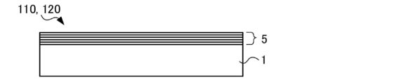
- FIG. 1 is a schematic view showing an example of a substrate 110 with a multilayer reflective film, which is an example of the substrate 120 with a thin film of the present embodiment.
- the substrate 110 with a multilayer reflective film shown in FIG. 1 includes a multilayer reflective film 5.
- the multilayer reflective film 5 of the substrate 110 with the multilayer reflective film is a predetermined thin film.
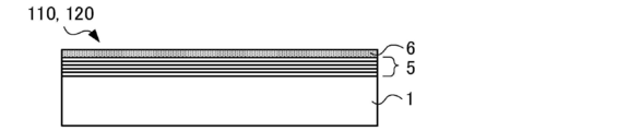
- FIG. 2 is a schematic view showing an example of a substrate 110 with a multilayer reflective film, which is another example of the substrate 120 with a thin film of the present embodiment.
- the substrate 110 with a multilayer reflective film shown in FIG. 2 includes a multilayer reflective film 5 and a protective film 6.
- the multilayer reflective film 5 and / or the protective film 6 of the substrate 110 with the multilayer reflective film is a predetermined thin film.
- FIG. 3 is a schematic view showing an example of the substrate with a thin film 120 (the substrate with a backside conductive film) of the present embodiment.
- the substrate 120 with a thin film shown in FIG. 3 includes a back surface conductive film 2.
- the back surface conductive film 2 of the thin film-attached substrate 120 is a predetermined thin film.
- FIG. 4 is a schematic view showing still another example of the substrate 110 with a multilayer reflective film, which is an example of the substrate 120 with a thin film of the present embodiment.
- the substrate 110 with a multilayer reflective film shown in FIG. 4 includes a back surface conductive film 2, a multilayer reflective film 5, and a protective film 6.
- at least one of the back surface conductive film 2, the multilayer reflective film 5, and the protective film 6 is a predetermined thin film.
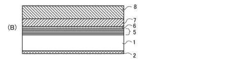
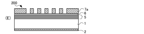
- FIG. 5 is a schematic view showing an example of a reflective mask blank 100, which is an example of the substrate with a thin film 120 of the present embodiment.
- the reflective mask blank 100 shown in FIG. 5 includes a back surface conductive film 2, a multilayer reflective film 5, a protective film 6, and an absorber film 7.
- at least one of the back surface conductive film 2, the multilayer reflective film 5, the protective film 6 and the absorber film 7 is a predetermined thin film.
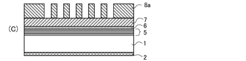
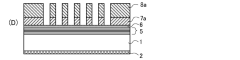
- FIG. 6 is a schematic view showing another example of the reflective mask blank 100, which is an example of the substrate with a thin film 120 of the present embodiment.
- the reflective mask blank 100 shown in FIG. 6 includes a back surface conductive film 2, a multilayer reflective film 5, a protective film 6, an absorber film 7, and an etching mask film 9.
- at least one of the back surface conductive film 2, the multilayer reflective film 5, the protective film 6, the absorber film 7, and the etching mask film 9 is a predetermined thin film.
- the "board 110 with a multilayer reflective film” means a substrate in which a multilayer reflective film 5 is formed on a predetermined substrate 1. 1 and 2 show an example of a schematic cross-sectional view of the substrate 110 with a multilayer reflective film.
- the "board 110 with a multilayer reflective film” includes a thin film other than the multilayer reflective film 5, such as a protective film 6 and / or a back surface conductive film 2.
- the "reflective mask blank 100” refers to a substrate with a multilayer reflective film 110 having an absorber film 7 formed on the multilayer reflective film 5.
- the “reflective mask blank 100” includes a structure in which a further thin film is formed, such as an etching mask film 9 and a resist film 8 (see FIGS. 6 and 7B).
- the main surface on which the back surface conductive film 2 is formed may be referred to as a "back side main surface” or a “second main surface”. Further, in the present specification, the main surface on which the back surface conductive film 2 of the substrate with the back surface conductive film is not formed may be referred to as “front side main surface” (or "first main surface”).
- front side main surface or "first main surface”.
- a multilayer reflective film 5 in which high refractive index layers and low refractive index layers are alternately laminated is formed on the front main surface of the mask blank substrate 1.
- providing (having) a predetermined thin film on the main surface of the mask blank substrate 1 means that the predetermined thin film is arranged in contact with the main surface of the mask blank substrate 1.
- the case of having another film between the mask blank substrate 1 and the predetermined thin film is also included.
- films other than the predetermined thin film For example, “having a film B on the film A” means that the film A and the film B are arranged so as to be in direct contact with each other, and another film is provided between the film A and the film B. Including the case of having.
- the film A is arranged in contact with the surface of the film B
- the film A and the film B are placed between the film A and the film B without interposing another film. It means that they are arranged so as to be in direct contact with each other.
- Rms (Root means square), which is a typical index of surface roughness, is the root mean square roughness, which is the square root of the value obtained by averaging the square of the deviation from the mean line to the measurement curve. Rms is expressed by the following equation (1).
- l is the reference length and Z is the height from the average line to the measurement curve.
- Rms has been conventionally used for controlling the surface roughness of the mask blank substrate 1, and the surface roughness can be grasped numerically.
- the substrate 120 with a thin film of the present embodiment includes a predetermined thin film on at least one main surface of the two main surfaces of the substrate 1.
- the substrate 120 with a thin film shown in FIGS. 1 and 2 is also referred to as a substrate 110 with a multilayer reflective film.
- the substrate with a thin film 120 shown in FIG. 3 is also referred to as a substrate with a backside conductive film.
- the substrate with a thin film 120 shown in FIGS. 5 and 6 is also referred to as a reflective mask blank 100.
- any one of the thin films formed on the substrate 120 with a thin film is a predetermined thin film.
- the predetermined thin film is preferably at least one selected from the back surface conductive film 2, the multilayer reflective film 5, the protective film 6, the absorber film 7, and the etching mask film 9. Further, the predetermined thin film is more preferably a multilayer reflective film 5 and / or a protective film 6.
- the predetermined thin film is a thin film (thin film such as the multilayer reflective film 5 and the protective film 6) usually used when forming the reflective mask blank 100, so that the performance of the reflective mask 200 is improved. Therefore, it is possible to manufacture a reflective mask 200 that does not have an adverse effect.
- the predetermined thin film contained in the substrate 120 with a thin film of the present embodiment includes a base material constituting the thin film and a trace amount material other than the base material.
- the “matrix material” is a main material among the materials forming the thin film, and the thin film is subjected to time-of-flight secondary ion mass spectrometry (TOF-SIMS: Time-Of).
- TOF-SIMS Time-Of
- -Flight Secondary Ion Mass Spectrometry is the material that corresponds to the highest signal strength.
- the signal intensity of TOF-SIMS is not necessarily proportional to the content in the thin film measured by other analytical methods.
- the atomic ratios of Mo and Si are about 40 atomic% and 60 atomic% as measured by X-ray photoelectron spectroscopy (XPS).
- the base material of the Mo / Si multilayer reflective film 5 in the present embodiment is Mo.
- the base material as described above may be referred to as a "base material constituting a thin film”.
- the "small-amount material” is a material other than the base material contained in the thin film. More specifically, it can mean a material (element) whose content in the thin film is 3 atomic% or less as measured by XPS, which is a material other than the base material.
- the atomic ratio of Si is about 60 atomic%, so it can mean that Si is neither a base material nor a trace material.
- impurities contained in a thin film have been considered to have an adverse effect on the performance of the thin film. Therefore, efforts have been made to reduce the concentration of impurities contained in the thin film as much as possible (ideally to be zero). If the content of the trace material (impurities) contained in the thin film of the thin film-attached substrate 120 is within a predetermined range, the present inventors have a comparison with the performance of the reflective mask 200 manufactured by using the thin-film-attached substrate 120. It was found that it does not have an adverse effect.
- the present inventors consider that the trace material (impurities) contained in the thin film of the thin film-attached substrate 120 is a predetermined material and the content thereof is not more than a predetermined range, the trace material (impurities) is contained in the thin film. ) Does not adversely affect the performance of the reflective mask 200, or the performance of the reflective mask 200 can be improved by the presence of trace materials (impurities) in the thin film. I found.
- an impurity that does not have an adverse effect even if it is present in the thin film or that can improve the performance of the reflective mask 200 by being present can be referred to as a trace material.
- the content of trace materials is often extremely low, and it is necessary to measure by a highly sensitive measuring method. Specifically, the content of the trace material can be determined by the time-of-flight secondary ion mass spectrometry (TOF-SIMS) described below.
- the measurement is performed using a time-of-flight secondary ion mass spectrometry (TOF-SIMS).
- TOF-SIMS time-of-flight secondary ion mass spectrometry
- the ratio of secondary ionic strength (I 2 / I 1 ) of the predetermined thin film is preferably larger than 0, more preferably 0.005 or more.
- the ratio (I 2 / I 1 ) is preferably 0.300 or less, more preferably 0.250 or less, and even more preferably 0.200 or less.
- Time-of-flight secondary ion mass spectrometry for measuring the secondary ionic strength (I 1 ) of the base material of a given thin film and at least one secondary ionic strength (I 2) of the trace material.
- the measurement conditions according to the above can be as shown below.
- Primary ion irradiation area Inner area of a quadrangle with a side of 200 ⁇ m
- Secondary ion measurement range 0.5 to 3000 m / z
- the secondary ionic strength can be measured by ion-etching the surface of the predetermined thin film by 1 to 2 nm.
- the secondary ion strength of the predetermined thin film is increased by removing the other film by ion etching to expose the predetermined thin film. Can be measured.
- the content of trace materials in a predetermined thin film is often extremely small. Therefore, the secondary ionic strength obtained by TOF-SIMS tends to vary depending on the measurement conditions.
- the ratio of secondary ionic strength (I 2 / I 1 ) obtained by TOF-SIMS is used, variation due to measurement conditions can be suppressed. Therefore, by using the ratio of secondary ionic strength (I 2 / I 1 ) obtained by TOF-SIMS, the performance of the reflective mask 200 is not adversely affected, or the performance of the reflective mask 200 is improved.
- the abundance of trace materials in the thin film that can be made can be appropriately defined.
- the lower limit of the content of trace materials (impurities) in a predetermined thin film is ideally preferably zero.
- components inside the film forming chamber such as a shield are exposed to plasma, an ion beam, and the like. Therefore, it is very difficult to reduce the content of the trace material derived from the material inside the chamber in the predetermined thin film to zero in consideration of cost and production efficiency. Therefore, in the present embodiment, it is decided that a predetermined trace amount of material is contained so as not to have an adverse effect even if it is present in the thin film, or to improve the performance of the reflective mask 200 by being present.
- the lower limit of the ratio of next ionic strength (I 2 / I 1 ) was set to a value larger than 0.
- the ratio of the secondary ionic strength (I 2 / I 1 ) is larger than 0.300, the defects of the thin film-attached substrate 120 increase, which may adversely affect the performance of the thin-film-attached substrate 120.
- the predetermined thin film is a multilayer reflective film and / or a protective film and the ratio of secondary ionic strength (I 2 / I 1 ) is larger than 0.300, the reflectance of EUV light decreases. Therefore, it is not preferable.
- the trace material of the predetermined thin film of the substrate 120 with a thin film of the present embodiment is yttrium (Y), zirconium (Zr), niobium (Nb), aluminum (Al), titanium (Ti), chromium (Cr), iron (Fe). ), Nickel (Ni) and copper (Cu) are preferably contained.
- the extinction coefficient k of yttrium (Y), zirconium (Zr) and niobium (Nb) at a wavelength of 13.5 nm is relatively low. Therefore, when these trace materials are contained in, for example, the multilayer reflective film 5 and / or the protective film 6, the effect of the multilayer reflective film 5 on the EUV light is small. Further, the inclusion of these trace materials in the predetermined thin film may contribute to the improvement of the durability of the predetermined thin film. In particular, when the trace material is yttrium (Y), the etching resistance of the predetermined thin film is increased, which is preferable.
- the extinction coefficient k of the trace material is preferably less than 0.01 and preferably 0.005 or less. More preferred.
- the extinction coefficient k of aluminum (Al), titanium (Ti), chromium (Cr), iron (Fe), nickel (Ni) and copper (Cu) at a wavelength of 13.5 nm is relatively high.
- the content of the trace material contained in the predetermined thin film is trace amount (the ratio of secondary ionic strength (I 2 / I 1 ) is equal to or less than the predetermined value) as described above, the reflective mask 200 There is little effect on the reflectance for EUV light. Further, the inclusion of these trace materials may reduce the stress difference at the interface between the predetermined thin film and another thin film or the like. Further, when these trace materials are contained, there is a tendency to inhibit the crystallization of a predetermined thin film.
- the crystal structure of the predetermined thin film can be easily amorphized. By amorphizing the crystal structure, the surface roughness of a predetermined thin film can be reduced.
- the extinction coefficient k of the trace material is preferably 0.01 or more.
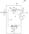
- FIG. 8 shows an example of a schematic diagram of the internal structure of the ion beam sputtering apparatus 500.
- An example of the ion beam sputtering apparatus 500 that can be used for forming a predetermined thin film of the present embodiment will be described with reference to FIG.
- the ion beam sputtering apparatus 500 that can be used in this embodiment includes a substantially rectangular vacuum chamber 502.
- One side of the vacuum chamber 502 (a wall surface having the lower side of FIG. 8 as one side; hereinafter, for convenience of explanation, appropriately referred to as "lower side") is provided with a substrate holder 503 via a holder mounting rod 504.
- the substrate holder 503 is configured to rotate while holding the substrate 1, which will be described in detail later.
- the substrate holder 503 includes a top clamp 517 provided with a pressing pin 518 at a corner portion.
- the substrate 1 is arranged on the substrate holder 503.
- the substrate 1 is clamped by pressing a corner of the main surface of the substrate 1 with a pressing pin 518 of the top clamp 517.
- the top clamp 517 has a function of holding the substrate 1 together with the substrate holder 503. Further, the top clamp 517 has a function of suppressing film adhesion to the side surface of the substrate 1 (similar function to the shield 519 described later).
- the material of the top clamp 517 is preferably an insulating material, for example, a resin material from the viewpoint of pressing the substrate 1 and suppressing dust generation. Further, among the resins, a material having a relatively high hardness is preferable, and for example, a polyimide-based resin is particularly preferable.
- a base 506 having a substantially rectangular shape in a plan view is placed on a substrate. It is arranged so as to face the holder 503.
- the first sputtering target 507 is arranged on one long side (the surface including one long side) of the base 506.
- a second sputtering target 508 is arranged on the other long side of the base 506 (the surface including the other long side).
- the material constituting the first sputtering target 507 and the second sputtering target 508 a metal, an alloy, a non-metal, or a compound thereof can be used in order to form a predetermined thin film in the mask blank.
- a metal, an alloy, a non-metal, or a compound thereof can be used.
- a multilayer reflective film 5 in which high refractive index materials and low refractive index materials are alternately laminated can be formed as a predetermined thin film.
- a high refractive index material such as silicon (Si) can be used as the material constituting the first sputtering target 507.
- a low refractive index material such as molybdenum (Mo) can be used as the material constituting the second sputtering target 508.
- the ion beam sputtering apparatus 500 will be described by taking as an example a case where a Si material is used for the first sputtering target 507 and a Mo material is used for the second sputtering target 508. Further, since the rotating shaft 509 is arranged at the center of the base 506, the base 506 can rotate integrally with the rotating shaft 509.
- An exhaust passage 510 in which a vacuum pump 511 is arranged is connected to one longitudinal surface of the vacuum chamber 502 (a wall surface having the left side in FIG. 8 as one side; hereinafter, appropriately referred to as a "left longitudinal surface"). Further, a valve (not shown) is provided in the exhaust passage 510 so as to be openable and closable.
- a pressure sensor 512 for measuring the pressure in the vacuum chamber 502 was ionized.
- Ion sources 505 for supplying particles are respectively arranged.
- the ion source 505 is connected to a plasma gas supply means (not shown). Ion particles of plasma gas are supplied from this plasma gas supply means.
- the multilayer reflective film 5 is a Mo / Si periodic multilayer film, ion particles of an inert gas such as argon ion, krypton ion, or xenon ion can be used as the ion particles.
- the ion source 505 is arranged so as to face the base 506.
- the ion source 505 is configured to supply the ion particles supplied from the plasma gas supply means to either the sputtering target 507 or 508 of the base 506.
- a neutralizer 513 is arranged to supply electrons for neutralizing the ion particles from the ion source 505.
- the neutralizer 513 is provided with an electron supply source (not shown) that draws electrons from the plasma of a predetermined gas.
- the electron source is configured to irradiate electrons in the path of the ion particles from the ion source 505 to the sputtering target 507 or 508. Not all ionic particles are necessarily neutralized by the neutralizer 513. Therefore, in the present specification, the term "ion particle" is also used for the ion particle partially neutralized by the neutralizer 513.
- Each device such as the holder mounting rod 504, the ion source 505, the rotary shaft 509, the vacuum pump 511, and the pressure sensor 512 is connected to a control device (not shown), and the operation is controlled by this control device. Has been done.
- a shield 519 is arranged in the vacuum chamber 502. Along with the above-mentioned top clamp 517, the shield 519 is arranged to prevent the occurrence of defects in the thin film formed on the substrate 1 due to the peeling of the adhered film.
- the surface of the shield 519 is exposed to a beam of ionized particles and the like. Therefore, the substance on the surface of the shield 519 is knocked out, and a part of the substance is contained in the thin film.
- the predetermined substance can be contained in a predetermined thin film as a predetermined trace material.
- the shield 519 can be placed in a portion exposed to a beam of ionized particles or the like. Therefore, by arranging a substance corresponding to a predetermined trace material on the surface of the shield 519, the predetermined trace material can be contained in the predetermined thin film. Further, with respect to the constituent members other than the shield 519 arranged in the vacuum chamber 502, the substance on the surface of the constituent members may be knocked out and contained in the predetermined thin film as in the case of the shield 519. By covering most of the area for forming the film of the vacuum chamber 502 with the shield 519, the influence of the constituent members other than the shield 519 can be avoided. Therefore, by controlling the predetermined trace material arranged on the surface of the shield 519, the type and content of the trace material contained in the predetermined thin film can be controlled.
- the shield 519 can be formed of a material containing the substance corresponding to the predetermined trace material. Further, by spraying a substance corresponding to the trace material on the surface of the shield 519, a film containing the trace material can be formed.
- a substance corresponding to the trace material on the surface of the shield 519
- a film containing the trace material can be formed.
- the shield 519 of the material containing yttrium (Y) yttria (Y 2 O 3 ) is sprayed on the surface of the shield 519 made of a stainless steel material suitable for a vacuum container such as SUS314 or SUS316.
- a shield 519 having a yttria (Y 2 O 3 ) coating formed on the surface of the shield 519 or the like can be used.
- a substance corresponding to the predetermined trace amount of material can be arranged on the surface of the shield 519.
- the surface of the shield 519 of SUS314 or SUS316 by blasting with blasting material of yttria (Y 2 O 3), it is possible to arrange the yttria (Y 2 O 3) on the surface of the shield 519 ..
- the concentration of the trace material in the predetermined thin film is the type and energy of the ion particles, the pressure during film formation, the concentration of the trace material on the surface of the shield 519, the shield 519 exposed to the beam of ionized particles, and the like. It can be controlled by changing the film forming conditions such as the area and shape of the shield 519 and the relative positional relationship between the shield 519 and the substrate 1.
- the concentration of the trace material in the predetermined thin film is the ratio of the secondary ionic strength (I 2 ) of the trace material to the secondary ionic strength (I 1 ) of the base material (I 2) measured by TOF-SIMS. It can be evaluated using I 2 / I 1).
- the vacuum pump 511 is operated to discharge gas from the vacuum chamber 502 through the exhaust passage 510. Then, the pressure in the vacuum chamber 502 measured by the pressure sensor 512 reaches a predetermined vacuum degree (vacuum degree that does not affect the characteristics of the film to be formed, for example, 10-8 Torr (1.33 ⁇ 10-6 Pa)). Wait until.
- a predetermined vacuum degree vacuum degree that does not affect the characteristics of the film to be formed
- the substrate 1 which is a substrate for forming a thin film is introduced into the vacuum chamber 502 via a robot arm (not shown), and is housed in the opening of the substrate holder 503 so that the main surface of the substrate 1 is exposed. .. Then, the substrate 1 arranged in the substrate holder 503 is clamped by pressing the corner of the main surface of the substrate 1 with the pressing pin 518 of the top clamp 517.
- the inside of the robot arm accommodating chamber (not shown) adjacent to the vacuum chamber 502 is also maintained in a predetermined vacuum state. Therefore, the vacuum chamber 502 can be held in the above-mentioned vacuum state even when the substrate 1 is introduced.
- the plasma gas for example, krypton plasma gas
- the degree of vacuum of the vacuum chamber 502 is controlled so as to be maintained at 10 -4 to 10-2 Torr (1.33 ⁇ 10-2 to 1.33 Pa) suitable for performing sputtering.
- the particles ionized from the ion source 505 (for example, Kr + particles) are supplied to the first sputtering target 507 arranged on the base 506.
- the particles are made to collide with the first sputtering target 507, and the Si particles constituting the target 507 are beaten (sputtered) from the surface thereof, and the Si particles are attached to the main surface of the substrate 1.
- the neutralizer 513 is actuated to neutralize the ionized particles (Kr + particles).
- the rod 504 of the substrate holder 503 and the rod 504 of the substrate holder 503 are arranged so that the rod 504 of the substrate holder 503 rotates at a predetermined rotation speed and the inclination angle of the first sputtering target 507 fluctuates within a certain range.
- the rotation shaft 509 of the base 506 is controlled by the control device.
- a Si film can be uniformly formed on the main surface of the substrate 1.
- a part of the surface of the shield 519 is exposed to the ionized particles. Therefore, the substance on the surface of the shield 519 is knocked out, and a part of the substance is contained in the Si film as a trace material.
- the rotation shaft 509 of the base 506 is rotated by approximately 180 ° to make the second sputtering target 508 face the main surface of the substrate 1.
- the particles ionized from the ion source 505 are supplied to the second sputtering target 508 arranged on the base 506.
- the Mo particles constituting the target 508 are beaten (sputtered) from the surface by the ionized particles, and the Mo particles are attached to the Si film surface formed on the main surface of the substrate 1.
- the neutralizer 513 is actuated to neutralize the ionized particles (eg Kr + particles).
- the Mo film having a uniform thickness is formed on the Si film formed on the substrate 1. Can be formed. Also at this time, a part of the surface of the shield 519 is exposed to the ionized particles as in the case of the Si film described above. Therefore, the substance on the surface of the shield 519 is knocked out, and a part of the substance is contained in the Mo film as a trace material.
- the Si film and the Mo film are alternately laminated with respect to EUV light which is an exposure light. A multilayer reflective film 5 having a predetermined reflectance is obtained.
- the predetermined thin film for example, the multilayer reflective film 5
- the multilayer reflection does not adversely affect the performance of the reflective mask 200.
- a thin film-attached substrate 120 having a film 5 (a substrate with a multilayer reflective film 110) can be obtained.
- the predetermined thin film of the thin film-attached substrate 120 of the present embodiment is at least one selected from the back surface conductive film 2, the multilayer reflective film 5, the protective film 6, the absorber film 7, and the etching mask film 9. It is preferably present, and more preferably the multilayer reflective film 5 and / or the protective film 6. Trace materials suitable for each of these thin films will be described in the description below.
- Substrate 110 with multilayer reflective film The substrate 1 constituting the substrate 110 with a multilayer reflective film, which is a kind of the substrate 120 with a thin film of the present embodiment, and each thin film will be described.
- the substrate 1 in the substrate 110 with a multilayer reflective film of the present embodiment needs to prevent the occurrence of the absorber pattern 7a distortion due to heat during EUV exposure. Therefore, as the substrate 1, a substrate 1 having a low coefficient of thermal expansion within the range of 0 ⁇ 5 ppb / ° C. is preferably used. As a material having a low coefficient of thermal expansion in this range, for example, SiO 2- TIO 2- based glass, multi-component glass ceramics, or the like can be used.
- the first main surface on the side on which the transfer pattern of the substrate 1 (the absorber film 7 described later constitutes this) is formed to have a predetermined flatness at least from the viewpoint of obtaining pattern transfer accuracy and position accuracy.
- the surface is processed.
- the flatness is preferably 0.1 ⁇ m or less, more preferably 0.05 ⁇ m or less, still more preferably 0.05 ⁇ m or less in the region of 132 mm ⁇ 132 mm on the main surface on the side where the transfer pattern of the substrate 1 is formed. It is 0.03 ⁇ m or less.
- the second main surface (back side main surface) opposite to the side on which the absorber film 7 is formed is a surface that is electrostatically chucked when set in the exposure apparatus.
- the flatness of the second main surface is preferably 0.1 ⁇ m or less, more preferably 0.05 ⁇ m or less, still more preferably 0.03 ⁇ m or less in a region of 132 mm ⁇ 132 mm.
- the flatness of the second main surface of the reflective mask blank 100 is preferably 1 ⁇ m or less, more preferably 0.5 ⁇ m or less, still more preferably 0.3 ⁇ m or less in the region of 142 mm ⁇ 142 mm. Is.
- the high surface smoothness of the substrate 1 is also an extremely important item.
- the surface roughness of the first main surface on which the absorber pattern 7a for transfer is formed is preferably 0.15 nm or less in root mean square roughness (Rms), and more preferably 0.10 nm or less in Rms.
- the surface smoothness can be measured with an atomic force microscope.
- the substrate 1 preferably has high rigidity in order to prevent deformation of the film (multilayer reflective film 5 or the like) formed on the substrate 1 due to film stress.
- the substrate 1 preferably has a high Young's modulus of 65 GPa or more.
- the substrate 110 with a multilayer reflective film of the present embodiment can have a base film in contact with the surface of the substrate 1.
- the base film is a thin film formed between the substrate 1 and the multilayer reflective film 5.
- the material of the base film a material containing ruthenium or tantalum as a main component is preferably used.
- the material of the base film can be, for example, Ru metal alone or Ta metal alone.
- the material of the base film is Ru or Ta, titanium (Ti), niobium (Nb), molybdenum (Mo), zirconium (Zr), yttrium (Y), boron (B), lantern (La), cobalt (Co). ) And / or a Ru alloy or Ta alloy containing a metal such as renium (Re).
- the film thickness of the base film is preferably in the range of, for example, 1 nm to 10 nm.
- the base film can be a predetermined thin film. That is, when the base film is measured by the time-of-flight secondary ion mass spectrometry (TOF-SIMS), the secondary ionic strength (I 1) of the base material when the secondary ionic strength released from the base film is measured.
- the ratio (I 2 / I 1 ) of at least one secondary ionic strength (I 2 ) of the trace material in the thin film to) is preferably in the above-mentioned predetermined range.
- the multilayer reflective film-attached substrate 110 (thin film-attached substrate 120) of the embodiment includes the multilayer reflective film 5.
- the multilayer reflective film 5 imparts a function of reflecting EUV light in the reflective mask 200.
- the multilayer reflective film 5 is a multilayer film in which each layer containing elements having different refractive indexes as main components is periodically laminated.
- the substrate 110 with a multilayer reflective film including the multilayer reflective film 5 is one kind of the substrate 120 with a thin film of the present embodiment. In the present embodiment, it is preferable that the multilayer reflective film 5 is a predetermined thin film.
- the multilayer reflective film 5 a thin film of a light element or a compound thereof (high refractive index layer) which is a high refractive index material and a thin film of a heavy element or a compound thereof which is a low refractive index material (low refractive index layer). ) And are alternately laminated for about 40 to 60 cycles, and a multilayer film is used.
- the multilayer film used as the multilayer reflective film 5 is formed by laminating a laminated structure of a high refractive index layer / a low refractive index layer in which a high refractive index layer and a low refractive index layer are laminated in this order from the substrate 1 side for a plurality of cycles.
- the laminated structure of the low refractive index layer / high refractive index layer in which the low refractive index layer and the high refractive index layer are laminated in this order from the substrate 1 side may be laminated for a plurality of cycles.
- the outermost surface layer of the multilayer reflective film 5, that is, the surface layer of the multilayer reflective film 5 on the side opposite to the substrate 1 side is preferably a high refractive index layer.
- the uppermost layer is It becomes a low refractive index layer.
- the low refractive index layer constitutes the outermost surface of the multilayer reflective film 5
- the laminated structure of the low refractive index layer / high refractive index layer in which the low refractive index layer and the high refractive index layer are laminated in this order from the substrate 1 side is set as one cycle, it is the most.
- the upper layer is a high refractive index layer. Therefore, in this case, it is not necessary to form a further high refractive index layer.
- a layer containing silicon (Si) can be used as the high refractive index layer.
- a material containing Si a Si compound containing boron (B), carbon (C), nitrogen (N), oxygen (O) and / or hydrogen (H) may be used in addition to Si alone. it can.
- a high refractive index layer containing Si a reflective mask 200 having excellent reflectance of EUV light can be obtained.
- a simple substance of a metal selected from molybdenum (Mo), ruthenium (Ru), rhodium (Rh), and platinum (Pt), or an alloy thereof can be used as the low refractive index layer.
- the low refractive index layer is a molybdenum (Mo) layer and the high refractive index layer is a silicon (Si) layer.
- Mo molybdenum
- Si silicon
- the multilayer reflective film 5 for reflecting EUV light having a wavelength of 13 nm to 14 nm a Mo / Si periodic laminated film in which Mo layers and Si layers are alternately laminated for about 40 to 60 cycles is preferably used.
- the high-refractive index layer which is the uppermost layer of the multilayer reflective film 5, is formed of silicon (Si), and a silicon oxide layer containing silicon and oxygen is formed between the uppermost layer (Si) and the protective film 6. can do.
- the mask cleaning resistance can be improved.
- the reflectance of the multilayer reflective film 5 alone is usually 65% or more, and the upper limit is usually 73%.
- the film thickness and period of each constituent layer of the multilayer reflective film 5 can be appropriately selected depending on the exposure wavelength. Specifically, the film thickness and period of each constituent layer of the multilayer reflective film 5 can be selected so as to satisfy Bragg's law of reflection.
- the film thickness of the high refractive index layers or the film thickness of the low refractive index layers does not necessarily have to be the same.
- the film thickness of the Si layer on the outermost surface of the multilayer reflective film 5 can be adjusted within a range that does not reduce the reflectance.
- the film thickness of Si (high refractive index layer) on the outermost surface can be 3 nm to 10 nm.
- the multilayer reflective film 5 of the substrate 110 with the multilayer reflective film is a predetermined thin film. That is, when the multilayer reflective film 5 is measured by the time-of-flight secondary ion mass spectrometry (TOF-SIMS), the secondary ions of the base material when the intensity of the secondary ions emitted from the multilayer reflective film 5 is measured.
- the ratio (I 2 / I 1 ) of at least one secondary ionic strength (I 2 ) of the trace material in the thin film to the strength (I 1 ) is preferably in the above-mentioned predetermined range.
- the base material can be molybdenum (Mo).
- the multilayer reflective film 5 of the substrate 110 with the multilayer reflective film of the present embodiment has Mo / Si multilayer reflection having a low refractive index layer of a molybdenum (Mo) layer and a high refractive index layer of a silicon (Si) layer.
- the film 5 is preferable.
- the Mo / Si multilayer reflective film 5 is measured by TOF-SIMS, the signal intensity of Mo is higher than the signal intensity of Si. Therefore, Mo is a material corresponding to the highest signal intensity when the Mo / Si multilayer reflective film 5 is measured by time-of-flight secondary ion mass spectrometry (TOF-SIMS). Therefore, the base material can be molybdenum (Mo).
- the trace materials contained in the multilayer reflective film 5 of the substrate 110 with a multilayer reflective film (substrate 120 with a thin film) of the present embodiment include yttrium (Y), zirconium (Zr), niobium (Nb), aluminum (Al), and titanium ( It preferably contains at least one element selected from Ti), chromium (Cr), iron (Fe), nickel (Ni) and copper (Cu).
- the extinction coefficient k of yttrium (Y), zirconium (Zr) and niobium (Nb) at a wavelength of 13.5 nm is relatively low. Therefore, when these trace materials are contained in the multilayer reflective film 5, the effect on the reflectance of the multilayer reflective film 5 with respect to EUV light is small. Further, the inclusion of these trace materials in the multilayer reflective film 5 may contribute to the improvement of the durability of the multilayer reflective film 5. In particular, when the trace material is yttrium (Y), the etching resistance of the multilayer reflective film 5 is high, which is preferable. When such a material having a low extinction coefficient k is used as the trace material, the extinction coefficient k of the trace material is preferably less than 0.01, more preferably 0.005 or less.
- the extinction coefficient k of aluminum (Al), titanium (Ti), chromium (Cr), iron (Fe), nickel (Ni) and copper (Cu) at a wavelength of 13.5 nm is relatively high.
- the content of the trace material contained in the multilayer reflective film 5 is a trace amount (the ratio of secondary ionic strength (I 2 / I 1 ) is equal to or less than a predetermined value) as described above, the reflective mask 200 Has little effect on the reflectance of EUV light.
- the inclusion of these trace materials may reduce the stress difference at the interface between the multilayer reflective film 5 and another thin film or the like.
- the multilayer reflective film 5 contains these trace materials, it tends to inhibit the crystallization of the multilayer reflective film 5. Therefore, when the multilayer reflective film 5 contains these trace materials, the crystal structure of the multilayer reflective film 5 can be easily amorphized. Therefore, the surface roughness of the multilayer reflective film 5 can be reduced.
- the multilayer reflective film 5 is a Mo / Si multilayer reflective film 5 and contains at least one element selected from yttrium (Y), zirconium (Zr) and niobium (Nb) as a trace material
- the multilayer reflective film 5 The ratio (I 2 / ) of at least one secondary ionic strength (I 2 ) of the trace material in the thin film to the secondary ionic strength (I 1 ) of the base material (Mo) when the released secondary ionic strength is measured.
- I 1 ) is preferably larger than 0, more preferably 0.005 or more, and even more preferably 0.010 or more.
- the ratio (I 2 / I 1 ) is preferably 0.300 or less, more preferably 0.250 or less.
- the multilayer reflective film 5 is a Mo / Si multilayer reflective film 5, and the trace material is selected from aluminum (Al), titanium (Ti), chromium (Cr), iron (Fe), nickel (Ni), and copper (Cu).
- the trace material is selected from aluminum (Al), titanium (Ti), chromium (Cr), iron (Fe), nickel (Ni), and copper (Cu).
- the secondary ionic strength (I 1 ) of the base material (Mo) when the secondary ionic strength emitted from the multilayer reflective film 5 is measured.
- the ratio (I 2 / I 1 ) of one secondary ionic strength (I 2 ) is preferably larger than 0, and more preferably 0.005 or more.
- the ratio (I 2 / I 1 ) is preferably 0.300 or less, more preferably 0.250 or less.
- the multilayer reflective film 5 can be formed on the substrate 1 by the ion beam sputtering method.
- the ion beam sputtering apparatus 500 as shown in FIG. 8 described above, the multilayer reflective film 5 in which the high refractive index material and the low refractive index material are alternately laminated can be formed.
- the material constituting the first sputtering target 507 a material having a high refractive index of Si or a Si compound can be used.
- a material having a low refractive index such as Mo, Nb, Ru or Rh can be used.
- a Si material is used for the first sputtering target 507 and a Mo material is used for the second sputtering target 508 will be described.
- a Si layer having a film thickness of about 4 nm is formed on the substrate 1 using a Si target.
- a Mo layer having a film thickness of about 3 nm is formed using a Mo target.
- the Si layer and the Mo layer are laminated for 40 to 60 cycles with one cycle as one cycle to form the multilayer reflective film 5 (the outermost layer is the Si layer). When 60 cycles are used, the number of steps increases from 40 cycles, but the reflectance to EUV light can be increased.
- a shield 519 is arranged in the vacuum chamber 502.
- a trace material incorporated into the multilayer reflective film 5 has an extinction coefficient k such as Y, Zr and Nb. It can be a relatively low material. As a result, even when a trace amount of material is contained in the multilayer reflective film 5, the influence of the multilayer reflective film 5 on EUV light can be reduced.
- the shield 519 or the like is made of a material containing yttrium (Y), for example, Y 2 O 3 , Y is contained in the multilayer reflective film 5.
- yttrium (Y) is contained as a trace material in the multilayer reflective film 5 because the etching resistance is increased.
- the shield 519, etc. of the material contained yttrium (Y) is, for example, on the surface of the shield 519 of SUS314 or SUS316, by spraying the yttria (Y 2 O 3), yttria surface such as the shield 519 (Y 2 O The one having the film of 3) formed can be used. Further, by blasting the surface, such as the shield 519 using the particles of yttria (Y 2 O 3), on the surface of the shield 519 can be arranged yttria (Y 2 O 3).
- the reflectance of the multilayer reflective film 5 may decrease.
- Stainless steel contains Cr and Fe. Therefore, when the shield 519 is made of stainless steel, there is a high possibility that Cr and Fe are contained as trace materials in the predetermined thin film. Therefore, it is preferable that the surface treatment (film formation or blast treatment) of the shield 519 is performed so that the multilayer reflective film 5 does not increase the content of trace materials such as Cr and Fe.
- the multilayer reflective film 5 is likely to be amorphized. Therefore, the surface roughness of the multilayer reflective film 5 can be reduced.
- Al and / or Ti is selected as the trace material having a relatively high extinction coefficient k
- Al 2 O 3 and / or TiO 2 or the like can be used for the shield 519 or the like.
- the method for forming the multilayer reflective film 5 using the ion beam sputtering apparatus 500 having the above configuration is as described as the method for forming a predetermined thin film.
- the constituent members such as the shield 519 are exposed to a beam of ionized particles and the like. Therefore, it is difficult to prevent the formed multilayer reflective film 5 from containing a material (trace material) derived from the material inside the chamber such as the shield 519 in consideration of cost and production efficiency. Therefore, by controlling the multilayer reflective film 5 to contain a predetermined trace amount of material within a predetermined content range, the multilayer reflection film 5 having the multilayer reflective film 5 does not at least adversely affect the performance of the reflective mask 200.
- a substrate with a film 110 (a substrate with a thin film 120) can be obtained.
- the substrate 110 with a multilayer reflective film including the protective film 6 is a kind of the substrate 120 with a thin film of the present embodiment. In the present embodiment, it is preferable that the protective film 6 is a predetermined thin film.
- the protective film 6 is formed on the multilayer reflective film 5 in order to protect the multilayer reflective film 5 from dry etching and cleaning in the manufacturing process of the reflective mask 200 described later.
- the protective film 6 also has a function of protecting the multilayer reflective film 5 when correcting black defects in a mask pattern using an electron beam (EB).
- EB electron beam
- the protective film 6 has one layer.
- the protective film 6 has a laminated structure of three or more layers, the bottom layer and the top layer are layers made of, for example, a substance containing ruthenium (Ru), and a metal other than Ru is used between the bottom layer and the top layer. Alternatively, an alloy may be interposed.
- the protective film 6 is formed of, for example, a material containing ruthenium (Ru) as a main component.
- Materials containing ruthenium as the main component include Ru metal alone, Ru with titanium (Ti), niobium (Nb), molybdenum (Mo), zirconium (Zr), ittrium (Y), boron (B), and lantern (La).
- the protective film 6 made of a Ru-based material containing Ti it is possible to suppress the phenomenon that silicon, which is a constituent element of the multilayer reflective film 5, diffuses from the surface of the multilayer reflective film 5 to the protective film 6. Therefore, the surface roughness during mask cleaning is reduced, and the film is less likely to peel off. Since the reduction of surface roughness is directly linked to the prevention of the decrease in the reflectance of the multilayer reflective film 5 with respect to the EUV exposure light, it is important for improving the exposure efficiency and throughput of EUV exposure.
- the Ru content ratio of the Ru alloy used for the protective film 6 is 50 atomic% or more and less than 100 atomic%, preferably 80 atomic% or more and less than 100 atomic%, and more preferably 95 atomic% or more and less than 100 atomic%.
- the Ru content ratio of the Ru alloy is 95 atomic% or more and less than 100 atomic%, it is possible to suppress the diffusion of the constituent element (silicon) of the multilayer reflective film 5 with respect to the protective film 6.
- the protective film 6 in this case has a mask cleaning resistance, an etching stopper function when the absorber film 7 is etched, and a function of preventing the multilayer reflective film 5 from changing with time while sufficiently ensuring the reflectance of EUV light. It becomes possible to combine.
- EUV lithography since there are few substances that are transparent to the exposure light, it is not technically easy to use EUV pellicle to prevent foreign matter from adhering to the mask pattern surface. For this reason, pellicle-less operation that does not use pellicle has become the mainstream. Further, in EUV lithography, exposure contamination occurs such that a carbon film is deposited on the reflective mask 200 and an oxide film is grown due to EUV exposure. Therefore, when the reflective mask 200 is used in the manufacture of a semiconductor device, it is necessary to frequently perform cleaning to remove foreign matter and contamination on the reflective mask 200. For this reason, the reflective mask 200 for EUV exposure is required to have an order of magnitude more mask cleaning resistance than the transmissive mask for optical lithography.
- a cleaning liquid such as sulfuric acid, sulfuric acid hydrogen peroxide (SPM), ammonia, ammonia hydrogen peroxide (APM), OH radical cleaning water, and ozone water having a concentration of 10 ppm or less is used.
- SPM sulfuric acid hydrogen peroxide
- APIAM ammonia hydrogen peroxide
- OH radical cleaning water ozone water having a concentration of 10 ppm or less.
- the cleaning resistance to hydrogen peroxide is particularly high, and it becomes possible to meet the requirement for mask cleaning resistance.
- the film thickness of the protective film 6 is not particularly limited as long as it can function as the protective film 6. From the viewpoint of the reflectance of EUV light, the film thickness of the protective film 6 is preferably 1.0 nm to 8.0 nm, more preferably 1.5 nm to 6.0 nm.
- the protective film 6 of the substrate 110 with the multilayer reflective film is a predetermined thin film. That is, when the protective film 6 is measured by the time-of-flight secondary ion mass spectrometry (TOF-SIMS), the secondary ionic strength of the base material when the secondary ionic strength released from the protective film 6 is measured ( I 1) the ratio of the at least one secondary ion intensity of trace materials in the thin film with respect to (I 2) (I 2 / I 1), it is preferable that the predetermined range described above.
- TOF-SIMS time-of-flight secondary ion mass spectrometry
- the protective film 6 is a single Ru metal or Ru with titanium (Ti), niobium (Nb), molybdenum (Mo), zirconium (Zr), ruthenium (Y), boron (B), lantern (La), cobalt (Co). ), Renium (Re) and / or a Ru alloy containing a metal such as rhodium (Rh), at least one element selected from yttrium (Y), zirconium (Zr) and niobium (Nb) as trace materials. At least one of the trace materials in the thin film with respect to the secondary ion strength (I 1 ) of the base material (Ru metal alone or Ru alloy) when the secondary ion strength released from the protective film 6 is measured.
- I 1 secondary ion strength
- the ratio (I 2 / I 1 ) of the secondary ion intensity (I 2 ) is preferably larger than 0, more preferably 0.005 or more, and further preferably 0.010 or more.
- the ratio (I 2 / I 1 ) is preferably 0.300 or less, more preferably 0.250 or less.
- the protective film 6 is a single Ru metal or Ru with titanium (Ti), niobium (Nb), molybdenum (Mo), zirconium (Zr), ruthenium (Y), boron (B), lantern (La), cobalt (Co). ), Ruthenium (Re) and / or Ruthenium containing metals such as rhodium (Rh), and as trace materials, aluminum (Al), titanium (Ti), chromium (Cr), iron (Fe), nickel.
- the secondary of the base material (Ru metal alone or Ru alloy) when the secondary ion intensity released from the protective film 6 is measured.
- the ratio (I 2 / I 1 ) of at least one secondary ion intensity (I 2 ) of the trace material in the thin film to the ion intensity (I 1 ) is preferably greater than 0, preferably 0.005 or greater. More preferred.
- the ratio (I 2 / I 1 ) is preferably 0.300 or less, more preferably 0.250 or less.
- the protective film 6 of the substrate 110 with a multilayer reflective film of the present embodiment is preferably formed of a material containing ruthenium (Ru) as a main component. Therefore, when the protective film 6 is a predetermined thin film, the base material can be ruthenium (Ru).
- the trace materials contained in the protective film 6 of the substrate 110 with a multilayer reflective film (the substrate with a thin film 120) of the present embodiment include yttrium (Y), zirconium (Zr), niobium (Nb), aluminum (Al), and titanium (Ti). ), Chromium (Cr), iron (Fe), nickel (Ni) and copper (Cu).
- the extinction coefficient k of yttrium (Y), zirconium (Zr) and niobium (Nb) at a wavelength of 13.5 nm is relatively low. Therefore, when these trace materials are contained in the protective film 6, the influence on the transmission of EUV light to the multilayer reflective film 5 formed under the protective film 6 is small. Further, the inclusion of these trace materials in the protective film 6 may contribute to the improvement of the durability of the protective film 6. In particular, when the trace material is yttrium (Y), the etching resistance of the protective film 6 is high, which is preferable. When such a material having a low extinction coefficient k is used as the trace material, the extinction coefficient k of the trace material is preferably less than 0.01, more preferably 0.005 or less.
- the extinction coefficient k of aluminum (Al), titanium (Ti), chromium (Cr), iron (Fe), nickel (Ni) and copper (Cu) at a wavelength of 13.5 nm is relatively high.
- the content of the trace material contained in the protective film 6 is trace amount (the ratio of secondary ionic strength (I 2 / I 1 ) is equal to or less than a predetermined value) as described above, the reflective mask 200 There is little effect on the reflectance for EUV light.
- the inclusion of these trace materials may reduce the stress difference at the interface between the protective film 6 and another thin film or the like.
- the protective film 6 contains these trace materials, it tends to inhibit the crystallization of the protective film 6. Therefore, when the protective film 6 contains these trace materials, the crystal structure of the protective film 6 can be easily amorphized. Therefore, the surface roughness of the protective film 6 can be reduced.
- a known film forming method can be adopted without particular limitation. Specific examples include a sputtering method and an ion beam sputtering method as a method for forming the protective film 6.
- the constituent members such as the shield 519 arranged in the film forming apparatus are exposed to a beam of ionized particles, plasma, or the like. Will be done. Therefore, it is difficult to prevent the formed protective film 6 from containing a material (trace material) derived from the material inside the chamber such as the shield 519 in consideration of cost and production efficiency. Therefore, a substrate with a multilayer reflective film having a protective film 6 that does not adversely affect the performance of the reflective mask 200 by controlling the protective film 6 to contain a predetermined trace amount of material within a predetermined content range. 110 (the substrate with a thin film 120) can be obtained. For that purpose, it is preferable that the material of the constituent member arranged inside the chamber such as the shield 519 is a material corresponding to a trace amount of material.
- the reflective mask blank 100 of the present embodiment will be described.
- the reflective mask blank 100 has an absorber film 7 on the above-mentioned substrate 110 with a multilayer reflective film.
- the reflective mask blank 100 including the absorber film 7, the multilayer reflective film 5, and optionally the protective film 6 is one of the thin film-attached substrates 120 of the present embodiment.
- the predetermined thin film is preferably at least one selected from the multilayer reflective film 5 and the protective film 6.
- the absorber membrane 7 can be a predetermined thin film.
- the absorber film 7 of the reflective mask blank 100 of the present embodiment is formed on the multilayer reflective film 5 (in the case where the protective film 6 is formed, on the protective film 6).
- the basic function of the absorber membrane 7 is to absorb EUV light.
- the absorber film 7 can be an absorber film 7 for the purpose of absorbing EUV light.
- the absorber film 7 can be an absorber film 7 having a phase shift function in consideration of the phase difference of EUV light.
- the absorber film 7 having a phase shift function absorbs EUV light and reflects a part of the EUV light to shift the phase.
- the portion where the absorber film 7 is formed absorbs EUV light and dims, and the pattern transfer is not adversely affected. Reflects some light. Further, in the region (field portion) where the absorber film 7 is not formed, EUV light is reflected from the multilayer reflection film 5 via the protective film 6. Therefore, a desired phase difference is obtained between the reflected light from the absorber film 7 having the phase shift function and the reflected light from the field portion.
- the absorber film 7 having a phase shift function is formed so that the phase difference between the reflected light from the absorber film 7 and the reflected light from the multilayer reflective film 5 is 170 degrees to 190 degrees.
- the image contrast of the projected optical image is improved by the light having the inverted phase difference in the vicinity of 180 degrees interfering with each other at the pattern edge portion.
- the resolution is increased, and various exposure-related margins such as exposure amount margin and focal margin can be increased.
- the absorber membrane 7 may be a single-layer membrane or a multilayer membrane composed of a plurality of membranes (for example, a lower-layer absorber membrane and an upper-layer absorber membrane).
- a single-layer film the number of steps during mask blank manufacturing can be reduced and the production efficiency is improved.
- its optical constant and film thickness can be appropriately set so that the upper layer absorber film becomes an antireflection film at the time of mask pattern defect inspection using light. This improves the inspection sensitivity at the time of mask pattern defect inspection using light.
- O oxygen
- N nitrogen
- the absorber film 7 is an absorber film 7 having a phase shift function, the range of adjustment on the optical surface can be increased by forming a multilayer film, so that a desired reflectance can be easily obtained. Become.
- the material of the absorber film 7 has a function of absorbing EUV light and can be processed by etching or the like (preferably, it can be etched by dry etching of chlorine (Cl) or fluorine (F) -based gas).
- etching or the like preferably, it can be etched by dry etching of chlorine (Cl) or fluorine (F) -based gas.
- Cl chlorine
- F fluorine
- Those having such a function include palladium (Pd), silver (Ag), platinum (Pt), gold (Au), iridium (Ir), tungsten (W), chromium (Cr), cobalt (Co), and manganese.
- Mn tin
- Sn tantalum
- Ta vanadium
- V nickel
- Hf hafnium
- Fe iron
- Cu tellurium
- Zn magnesium
- Mg germanium
- Al aluminum
- Rh rhodium
- Ru ruthenium
- Mo molybdenum
- Nb niobium
- Ti titanium
- Zr zirconium
- Y ittrium
- At least one metal selected from silicon (Si), or a compound (alloy) thereof can be preferably used.
- the absorber film 7 can be formed by a magnetron sputtering method such as a DC sputtering method and an RF sputtering method.
- the absorber film 7 such as a tantalum compound can be formed by a reactive sputtering method using a target containing tantalum and boron and using argon gas to which oxygen or nitrogen is added.
- the tantalum compound for forming the absorber film 7 includes an alloy of Ta and the above-mentioned metal.
- the crystalline state of the absorber membrane 7 is preferably an amorphous or microcrystalline structure from the viewpoint of smoothness and flatness. If the surface of the absorber film 7 is not smooth or flat, the edge roughness of the absorber pattern 7a may increase and the dimensional accuracy of the pattern may deteriorate.
- the surface roughness of the absorber film 7 is a root mean square roughness (Rms) of 0.5 nm or less, more preferably 0.4 nm or less, and further preferably 0.3 nm or less.
- the tantalum compound for forming the absorber film 7 includes a compound containing Ta and B, a compound containing Ta and N, a compound containing Ta, O and N, Ta and B, and further O.
- Ta is a material that has a large EUV light absorption coefficient and can be easily dry-etched with chlorine-based gas or fluorine-based gas. Therefore, it can be said that Ta is a material for the absorber membrane 7 having excellent processability. Further, by adding B, Si and / or Ge or the like to Ta, an amorphous material can be easily obtained. As a result, the smoothness of the absorber membrane 7 can be improved. Further, when N and / or O is added to Ta, the resistance of the absorber membrane 7 to oxidation is improved, so that the effect of improving the stability over time can be obtained.
- the predetermined thin film is at least one selected from the multilayer reflective film 5 and the protective film 6.
- the absorber film 7 is further formed on the multilayer reflective film 5 or the protective film 6 which is a predetermined thin film. The base material and trace material when the predetermined thin film is the multilayer reflective film 5 and the protective film 6 are as described above.
- the absorber film 7 can be a predetermined thin film. That is, when the absorber film 7 is measured by the time-of-flight secondary ion mass spectrometry (TOF-SIMS), the secondary ion of the base material when the intensity of the secondary ion released from the absorber film 7 is measured.
- the ratio (I 2 / I 1 ) of at least one secondary ionic strength (I 2 ) of the trace material in the thin film to the strength (I 1 ) can be in the predetermined range described above.
- the material of the absorber film 7 is palladium (Pd), silver (Ag), platinum (Pt), gold (Au), iridium (Ir), tungsten (W), chromium (Cr), cobalt (Co), manganese (Mn).
- the ratio (I 2 / I 1 ) of at least one secondary ion intensity (I 2 ) of the trace material in the thin film to) is preferably larger than 0, and more preferably 0.005 or more.
- the ratio (I 2 / I 1 ) is preferably 0.300 or less, more preferably 0.250 or less, and even more preferably 0.200 or less.
- the base material can be the above-mentioned main component metal.
- the content ratio of the metal as the main component is preferably 50 atomic% or more.
- the material of the absorber membrane 7 contains Ta
- aluminum (Al), titanium (Ti), chromium (Cr), iron (Fe), nickel (Ni) or copper (Cu) is contained as a trace material.
- the extinction coefficient k of aluminum (Al) or the like at a wavelength of 13.5 nm is relatively high. Therefore, when aluminum (Al) or the like is contained as a trace material in the absorber film 7, the extinction coefficient k at a wavelength of 13.5 nm becomes relatively high.
- the stress difference at the interface between the absorber film 7 and the thin film in contact with the absorber film 7 is increased. May shrink.
- a shield 519 for example, a stainless steel shield
- aluminum for example, aluminum (for example, a stainless steel shield)
- An absorber membrane 7 containing Al) as a trace material can be obtained.
- the trace material contained in the absorber film 7 of the reflective mask blank 100 of the present embodiment does not contain yttrium (Y) and zirconium (Zr). Therefore, in order to form the absorber film 7, the constituent members such as the shield 519 arranged in the film forming apparatus are formed of a material containing no yttrium (Y) and zirconium (Zr). Is preferable.
- Backside conductive film 2 Above the second main surface (back side main surface) of the substrate 1 (opposite the formation surface of the multilayer reflective film 5), and when an intermediate layer such as a hydrogen intrusion suppression film is formed on the substrate 1, the intermediate layer On the upper side), a back surface conductive film 2 for an electrostatic chuck is formed.
- the sheet resistance required for the back surface conductive film 2 for an electrostatic chuck is usually 100 ⁇ / ⁇ ( ⁇ / square) or less.
- the method for forming the back surface conductive film 2 is, for example, a magnetron sputtering method or an ion beam sputtering method using a target of a metal such as chromium or tantalum or an alloy thereof.
- the material containing chromium (Cr) in the back surface conductive film 2 is preferably a Cr compound containing at least one selected from boron, nitrogen, oxygen, and carbon in Cr.
- the Cr compound include CrN, CrON, CrCN, CrCON, CrBN, CrBON, CrBCN and CrBOCN.
- Ta (tantalum) of the back surface conductive film 2 Ta (tantalum), an alloy containing Ta, or a Ta compound containing at least one of boron, nitrogen, oxygen, and carbon in any of these is used. It is preferable to use it.
- Ta compounds include TaB, TaN, TaO, TaON, TaCON, TaBN, TaBO, TaBON, TaBCON, TaHf, TaHfO, TaHfN, TaHfON, TaHfCON, TaSi, TaSiO, TaSiN, TaSiN, TaSiN, and TaSiN. it can.
- the film thickness of the back surface conductive film 2 is not particularly limited as long as it satisfies the function for the electrostatic chuck, but is usually 10 nm to 200 nm.
- the back surface conductive film 2 also has stress adjustment on the second main surface side of the mask blank 100. That is, the back surface conductive film 2 is adjusted so as to obtain a flat reflective mask blank 100 by balancing the stress from various films formed on the first main surface side.
- the back surface conductive film 2 can be formed on the substrate 110 with the multilayer reflective film.
- a substrate 110 with a multilayer reflective film having a back surface conductive film 2 as shown in FIG. 3 can be obtained.
- the back surface conductive film 2 can be a predetermined thin film. Therefore, the substrate with a thin film 120 (the substrate with a backside conductive film) as shown in FIG. 3 is also one of the substrates 120 with a thin film of the present embodiment.
- the material of the back surface conductive film 2 is a Cr compound or a Ta compound, and a trace material includes aluminum (Al), titanium (Ti), chromium (Cr), iron (Fe), nickel (Ni) or copper (Cu).
- a trace material includes aluminum (Al), titanium (Ti), chromium (Cr), iron (Fe), nickel (Ni) or copper (Cu).
- the ratio of I 2 ) (I 2 / I 1 ) is preferably greater than 0, more preferably 0.005 or more.
- the ratio (I 2 / I 1 ) is preferably 0.300 or less, more preferably 0.250 or less.
- the base material can be Ta or Cr.
- the content ratio of Ta or Cr is preferably 50 atomic% or more.
- the material of the back surface conductive film 2 is a Ta compound
- aluminum (Al), titanium (Ti), chromium (Cr), iron (Fe), nickel (Ni) or copper (Cu) may be contained as trace materials.
- the electrical conductivity of aluminum (Al) and the like is high, it is possible to contribute to the conductivity of the back surface conductive film 2 by including aluminum (Al) and the like as a trace material in the back surface conductive film 2.
- the back surface conductive film 2 is required to have mechanical strength in order to perform vacuum chucking. Since aluminum (Al) or the like is contained as a trace material, the density of the film is increased by amorphization, and it becomes possible to improve the mechanical properties.
- a shield 519 for example, a stainless steel shield
- alumina (Al 2 O 3 ) blast material aluminum (for example, aluminum (for example, a stainless steel shield)) is formed. It is possible to obtain a back surface conductive film 2 containing Al) as a trace material.
- etching mask film 9 may be formed on the absorber film 7.
- a material having a high etching selectivity of the absorber film 7 with respect to the etching mask film 9 is used.
- the "etching selection ratio of B to A” refers to the ratio of the etching rate between A, which is a layer (mask layer) that is not desired to be etched, and B, which is a layer that is desired to be etched.
- etching selectivity of B with respect to A etching rate of B / etching rate of A”.
- high selection ratio means that the value of the selection ratio defined above is large with respect to the comparison target.
- the etching selectivity of the absorber film 7 with respect to the etching mask film 9 is preferably 1.5 or more, and more preferably 3 or more.
- Examples of the material having a high etching selectivity of the absorber film 7 with respect to the etching mask film 9 include a material of chromium and a chromium compound.
- a material of chromium or a chromium compound can be used.
- the chromium compound include a material containing Cr and at least one element selected from N, O, C and H.
- a material of silicon or a silicon compound can be used.
- Examples of the silicon compound include a material containing Si and at least one element selected from N, O, C and H, metallic silicon (metal silicide) containing a metal in silicon and the silicon compound, and metallic silicon compound (metal silicide). Materials such as compound) can be mentioned.
- Examples of the metal silicon compound include a material containing a metal, Si, and at least one element selected from N, O, C, and H.
- the film thickness of the etching mask film 9 is preferably 3 nm or more from the viewpoint of obtaining a function as an etching mask that accurately forms a transfer pattern on the absorber film 7. Further, the film thickness of the etching mask film 9 is preferably 15 nm or less from the viewpoint of reducing the film thickness of the resist film 8.
- the etching mask film 9 can be the above-mentioned predetermined thin film.
- the substrate with a thin film 120 of the present embodiment suppresses hydrogen from entering from the substrate 1 to the back surface conductive film 2 between the glass substrate which is the substrate 1 and the back surface conductive film 2 containing tantalum or chromium. It is preferable to provide a hydrogen intrusion suppression film.
- the presence of the hydrogen intrusion suppressing film can suppress the uptake of hydrogen into the back surface conductive film 2, and can suppress the increase in the compressive stress of the back surface conductive film 2.
- the material of the hydrogen intrusion suppression film may be any kind as long as it is difficult for hydrogen to permeate and can suppress the invasion of hydrogen from the substrate 1 to the back surface conductive film 2.
- Specific examples of the material for the hydrogen intrusion suppression membrane include Si, SiO 2 , SiON, SiCO, SiCON, SiBO, SiBON, Cr, CrN, CrON, CrC, CrCN, CrCO, CrCON, Mo, MoSi, and MoSiN. , MoSiO, MoSiCO, MoSiON, MoSiCON, TaO, TaON and the like.
- the hydrogen intrusion suppression film can be a single layer of these materials, or may be a plurality of layers and a composition gradient film.
- the hydrogen intrusion suppression film can be the above-mentioned predetermined thin film.
- the present embodiment is a reflective mask 200 in which the absorber film 7 in the above-mentioned reflective mask blank 100 is patterned and the absorber pattern 7a is provided on the multilayer reflective film 5.
- the reflective mask blank 100 of the present embodiment it is possible to obtain a reflective mask 200 that has no adverse effect on the performance of the reflective mask 200 or has improved performance of the reflective mask 200.
- the reflective mask 200 of the present embodiment is used to manufacture the reflective mask 200.
- the reflective mask 200 of the present embodiment is used to manufacture the reflective mask 200.
- a reflective mask blank 100 is prepared, and a resist film 8 is formed on the outermost surface of the first main surface thereof (on the absorber film 7 as described in the following examples) (as the reflective mask blank 100). (Not required when the resist film 8 is provided), a desired pattern such as a circuit pattern is drawn (exposed) on the resist film 8, and further developed and rinsed to form a predetermined resist pattern 8a.
- the absorber film 7 is dry-etched to form the absorber pattern 7a.
- the etching gas includes chlorine-based gas such as Cl 2 , SiCl 4 , and CHCl 3 , mixed gas containing chlorine-based gas and O 2 in a predetermined ratio, and chlorine-based gas and He in a predetermined ratio.
- Mixed gas containing, mixed gas containing chlorine-based gas and Ar in a predetermined ratio, CF 4 , CHF 3 , C 2 F 6 , C 3 F 6 , C 4 F 6 , C 4 F 8 , CH 2 F 2 , Fluorine-based gases such as CH 3 F, C 3 F 8 , SF 6 , and F 2 and a mixed gas containing a fluorine-based gas and O 2 in a predetermined ratio can be used.
- oxygen is contained in the etching gas at the final stage of etching, the surface of the Ru-based protective film 6 is roughened. Therefore, in the over-etching step where the Ru-based protective film 6 is exposed to etching, it is preferable to use an etching gas containing no oxygen.
- the resist pattern 8a is removed by ashing or a resist stripping solution to prepare an absorber pattern 7a in which a desired circuit pattern is formed.
- the reflective mask 200 of the present embodiment can be obtained.
- the present embodiment is a method for manufacturing a semiconductor device, which comprises a step of performing a lithography process using an exposure device using the above-mentioned reflective mask 200 to form a transfer pattern on a transfer target.
- the above-mentioned reflective mask 200 can be set in an exposure apparatus having an exposure light source that emits EUV light, and the transfer pattern can be transferred to a resist film formed on a substrate to be transferred.
- the method for manufacturing a semiconductor device of the present embodiment even if the thin film of the reflective mask 200 contains impurities (trace materials), the reflective mask 200 does not adversely affect the performance of the reflective mask 200. Since it can be used, it is possible to manufacture a semiconductor device having a fine and highly accurate transfer pattern.
- a desired transfer pattern can be formed on the semiconductor substrate by performing EUV exposure using the reflective mask 200 of the present embodiment.
- a semiconductor device in which a desired electronic circuit is formed is manufactured with a high yield by undergoing various processes such as etching of the film to be processed, forming of an insulating film, a conductive film, introduction of a dopant, and annealing. can do.
- Example 1 As Example 1, as shown in FIG. 2, a substrate 110 with a multilayer reflective film was produced in which a multilayer reflective film 5 and a protective film 6 were formed on one main surface of the substrate 1.
- the substrate 110 with the multilayer reflective film of Example 1 was produced as follows.
- a SiO 2- TiO 2 glass substrate which is a 6025 size (about 152 mm ⁇ 152 mm ⁇ 6.35 mm) low thermal expansion glass substrate in which both the first main surface and the second main surface are polished, is prepared, and the substrate 1 and the substrate 1 are prepared. did. Polishing was performed by a rough polishing process, a precision polishing process, a local processing process, and a touch polishing process so that the main surface was flat and smooth.
- the multilayer reflective film 5 and the protective film 6 were continuously formed on the first main surface of the substrate 1 described above.
- a shield 519 was arranged in the vacuum chamber 502 of the ion beam sputtering apparatus 500.
- a shield 519 made of SUS314 with a blasted surface was used as the shield 519.
- the blast material yttria (Y 2 O 3 ) particles were used.
- the shield 519 was cleaned by ultrasonic cleaning and / or plasma cleaning. Such blasting and cleaning process, the surface of the shield 519 and can be arranged yttria (Y 2 O 3).
- the multilayer reflective film 5 of Example 1 was a periodic multilayer reflective film 5 composed of Si and Mo in order to obtain a multilayer reflective film 5 suitable for EUV light having a wavelength of 13.5 nm.
- Si targets and Mo targets were used as targets for high refractive index materials and targets for low refractive index materials (first and second sputtering targets 507 and 508).
- Krypton (Kr) ion particles were supplied from the ion source 505 to these targets 507 and 508, and ion beam sputtering was performed to alternately laminate Si layers and Mo layers on the substrate 1.
- the substance contained in the shield 519 specifically, the material (chromium and iron) of SUS314 and the blast material (yttrium) are contained in the multilayer reflective film 5 as a trace material. Became.
- the sputtered particles of Si and Mo were incident on the normal of the main surface of the substrate 1 at an angle of 30 degrees.
- the Si layer was formed with a film thickness of 4.2 nm, and then the Mo layer was formed with a film thickness of 2.8 nm. This was set as one cycle, and the layers were laminated for 40 cycles in the same manner, and finally a Si layer was formed with a film thickness of 4.0 nm to form a multilayer reflective film 5. Therefore, the material of the lowermost layer of the multilayer reflective film 5, that is, the multilayer reflective film 5 closest to the substrate 1, is Si, and the material of the uppermost layer of the multilayer reflective film 5, that is, the multilayer reflective film 5 in contact with the protective film 6 is also Si. Is.
- the protective film 6 was continuously formed on the surface of the substrate 110 with the multilayer reflective film described above.
- a protective film 6 made of Ru was formed with a film thickness of 2.5 nm by an ion beam sputtering method using a Ru target.
- the sputtered particles of Ru were incident on the normal of the main surface of the substrate 1 at an angle of 40 degrees.
- the substance contained in the shield 519 specifically, the material (chromium and iron) of SUS314 and the blast material (yttrium) are contained in the protective film 6 as a trace material. became.
- annealing was performed at 130 ° C. in the air.
- the substrate 110 with the multilayer reflective film of Example 1 was manufactured.
- the portion corresponding to the protective film 6 and the multilayer reflective film 5 of the substrate 110 with the multilayer reflective film of Example 1 is subjected to time-of-flight secondary ion mass spectrometry (TOF-SIMS). Measured by Spectrometry). Specifically, after the surface of the protective film 6 was ion-etched by 1 nm, the secondary ionic strengths of the base material and the trace material were measured by TOF-SIMS of the protective film 6. Next, the protective film 6 is ion-etched, the multilayer reflective film 5 is exposed to the surface, and then further etched by 1 nm, and then the secondary ion strength of the base material and the trace material is measured by TOF-SIMS of the multilayer reflective film 5. did.
- TOF-SIMS time-of-flight secondary ion mass spectrometry
- Table 1 shows the types of base material and trace material measured by TOF-SIMS.
- the elements (Y, Fe and Cr) indicated by "*" are trace materials to be measured.
- the base material of the protective film 6 was Ru, and the base material of the multilayer reflective film 5 was Mo.
- the measurement conditions for TOF-SIMS are shown below.
- Primary ion irradiation area Inner area of a quadrangle with a side of 200 ⁇ m
- Secondary ion measurement range 0.5 to 3000 m / z
- Table 2 the ratio of the secondary ion intensity (I 1) and secondary ion intensity calculated from secondary ion intensity (I 2) of trace materials mother material (Ru) by measuring TOF-SIMS of the protective film 6 ( I 2 / I 1 ) is shown. Further, in Table 3, secondary ion intensity (I 1) and secondary ion intensity calculated from secondary ion intensity (I 2) of trace materials mother material by measuring TOF-SIMS multilayer reflective film 5 (Mo) The ratio of (I 2 / I 1 ) is shown.
- Y / Ru in Table 2 is the ratio (I 2 / ) of the secondary ionic strength (I 1 ) of Ru, which is a base material, to the secondary ionic strength (I 2) of Y, which is a trace material. It means I 1 ).
- the reflectance of the substrate 110 with a multilayer reflective film manufactured under the conditions of Example 1 with respect to EUV light having a wavelength of 13.5 nm was measured, and it was confirmed that there was no decrease in reflectance as compared with the reference example described later.
- the crystallinity of the Mo film of the substrate 110 with a multilayer reflective film manufactured under the conditions of Example 1 was measured by an X-ray diffractometer (XRD), and it was confirmed that the crystals were finer than those of the reference example. ..
- Example 1 shows the materials for manufacturing the substrate 110 with the multilayer reflective film of Examples 2 to 5.
- the substrate 110 with a multilayer reflective film in which the multilayer reflective film 5 and the protective film 6 were formed on the first main surface of the substrate 1 was manufactured.
- the shield 519 blasted with the particles of the materials shown in Table 1 was used.
- the thickness of the blasting treatment was adjusted to adjust the amount of the shield material contained in the multilayer reflective film 5 and the protective film 6.
- Example 4 a shield 519 which has not been blasted was used. Therefore, the trace amount material contained in the multilayer reflective film 5 and the protective film 6 of Examples 2 to 5 is different from that of Example 1.
- Example 1 Similar to Example 1, the portions corresponding to the protective film 6 and the multilayer reflective film 5 of the substrates 110 with the multilayer reflective film of Examples 2 to 5 are measured by time-of-flight secondary ion mass spectrometry (TOF-SIMS). did. Tables 2 and 3 show the measurement results. Further, similarly to Example 1, the reflectance of the substrate 110 with the multilayer reflective film 110 and the crystallinity of the Mo film of Examples 2 to 5 were measured. As a result, similarly to Example 1, the substrates 110 with the multilayer reflective film of Examples 2 to 5 did not have a decrease in reflectance as compared with the reference example, and were finer crystals than the reference example.
- TOF-SIMS time-of-flight secondary ion mass spectrometry
- Example 6 and 7 Table 1 shows the materials for manufacturing the substrate 110 with the multilayer reflective film of Examples 6 and 7.
- the substrate 110 with a multilayer reflective film in which the multilayer reflective film 5 and the protective film 6 were formed on the first main surface of the substrate 1 was manufactured.
- the protective film 6 was formed by the DC magnetron sputtering method.
- Example 6 the multilayer reflective film 5 was formed by the ion beam sputtering method using the ion beam sputtering apparatus 500 in the same manner as in Example 1. Then, the protective film 6 was formed by the DC magnetron sputtering method using a magnetron sputtering apparatus. Specifically, using a Ru target, a protective film 6 made of Ru was formed on the multilayer reflective film 5 with a film thickness of 2.5 nm by a DC sputtering method in an Ar gas atmosphere. At that time, the shields in the ion beam sputtering apparatus 500 and the magnetron sputtering apparatus were blasted with particles of the material (alumina (Al 2 O 3)) shown in Table 1. Therefore, it was decided to include aluminum (Al) as a measurement element by the time-of-flight secondary ion mass spectrometry (TOF-SIMS).
- TOF-SIMS time-of-flight secondary ion mass spectrometry
- Example 7 the multilayer reflective film 5 was formed by the ion beam sputtering method using the ion beam sputtering apparatus 500 as in Example 6. Then, in the same manner as in Example 6, the protective film 6 was formed by the DC magnetron sputtering method using a magnetron sputtering apparatus. Further, in Example 7, in the ion beam sputtering apparatus 500 and the magnetron sputtering apparatus, a shield which has not been blasted was used.
- a particle getter made of copper (Cu) is attached to a predetermined portion of the inner wall of the apparatus, particularly the ion beam sputtering apparatus 500 and the magnetron sputtering shield, and the Mo / Si multilayer reflective film 5 and The protective film 6 was formed. Therefore, it was decided to include copper (Cu) as a measurement element by the time-of-flight secondary ion mass spectrometry (TOF-SIMS).
- TOF-SIMS time-of-flight secondary ion mass spectrometry
- Example 1 Similar to Example 1, the portions corresponding to the protective film 6 and the multilayer reflective film 5 of the substrate 110 with the multilayer reflective film of Examples 6 and 7 are measured by the time-of-flight secondary ion mass spectrometry (TOF-SIMS). did. Tables 2 and 3 show the measurement results. Further, similarly to Example 1, the reflectance of the substrate 110 with the multilayer reflective film 110 and the crystallinity of the Mo film of Examples 6 and 7 were measured. As a result, similarly to Example 1, the substrates 110 with the multilayer reflective film of Examples 6 and 7 did not have a decrease in reflectance as compared with the reference example, and were more microcrystals.
- TOF-SIMS time-of-flight secondary ion mass spectrometry
- Reference example 1 Similar to Example 1, the substrate 110 with a multilayer reflective film of Reference Example 1 was manufactured. However, in Reference Example 1, when the multilayer reflective film 5 and the protective film 6 were formed, the material of the shield 519 arranged in the vacuum chamber 502 of the ion beam sputtering apparatus 500 was high-purity molybdenum (Mo). .. Further, by cleaning the surface of the shield 519 by etching, impurities were prevented from adhering to the surface of the shield 519. High-purity molybdenum (Mo) is much more expensive than Shield 519 made of SUS314. Therefore, the cost for manufacturing the substrate 110 with the multilayer reflective film of Reference Example 1 is much higher than that of Examples 1 to 7.
- Mo molybdenum
- Example 1 Similar to Example 1, the portion corresponding to the protective film 6 and the multilayer reflective film 5 of the substrate 110 with the multilayer reflective film of Reference Example 1 was measured by the time-of-flight secondary ion mass spectrometry (TOF-SIMS). Further, similarly to Example 1, the reflectance of the substrate 110 with the multilayer reflective film 110 of Reference Example 1 and the crystallinity of the Mo film were measured.
- the multilayer reflective film 5 of Reference Example 1 does not contain an element corresponding to a trace material (below the detection limit), and the protective film 6 contains trace materials other than molybdenum (Mo) below the detection limit. It was. Since the substrate 110 with a multilayer reflective film of Reference Example 1 had no problem as the substrate 110 with a multilayer reflective film for manufacturing a predetermined reflective mask 200, Reference Example 1 was used as a comparison target of Examples 1 to 7. did.
- the reflectance of the multilayer reflective film 5 did not decrease as compared with Reference Example 1. Further, regarding the crystallinity of the Mo film, it was confirmed that the crystal grains were finer crystallites as compared with Reference Example 1. Therefore, in Examples 1 to 7, even if the predetermined thin film of the substrate 110 with the multilayer reflective film for manufacturing the reflective mask 200 contains impurities (trace materials), the reflective mask 200 to be manufactured It can be said that it does not adversely affect the performance at least.
- the reflective mask blank 100 can be manufactured by using the substrates 110 with the multilayer reflective film of Examples 1 to 7 and Reference Example 1 described above. Hereinafter, a method for manufacturing the reflective mask blank 100 will be described.
- the absorber film 7 was formed on the protective film 6 of the substrate 110 with a multilayer reflective film by the DC magnetron sputtering method.
- the absorber film 7 was a laminated film 7 composed of two layers, a TaN film which is an absorption layer and a TaO film which is a low reflection layer.
- a TaN film was formed as an absorption layer on the surface of the protective film 6 of the substrate 110 with the multilayer reflective film described above by a DC magnetron sputtering method.
- This TaN film was formed by a reactive sputtering method in a mixed gas atmosphere of Ar gas and N 2 gas in which a substrate 110 with a multilayer reflective film was opposed to a Ta target.
- a TaO film (low reflection layer) was further formed on the TaN film by the DC magnetron sputtering method. Similar to the TaN film, this TaO film was formed by a reactive sputtering method in a mixed gas atmosphere of Ar and O 2 with the substrate 120 with a multilayer reflective film facing the Ta target.
- a back surface conductive film 2 made of CrN was formed on the second main surface (back side main surface) of the substrate 1 by a magnetron sputtering method (reactive sputtering method) under the following conditions.
- Conditions for forming the back surface conductive film 2 Cr target, mixed gas atmosphere of Ar and N 2 (Ar: 90 atomic%, N: 10 atomic%), film thickness 20 nm.
- the reflective mask blank 100 was manufactured using the substrates 110 with the multilayer reflective film of Examples 1 to 7 and Reference Example 1.
- Reflective mask 200 Next, the reflective mask 200 was manufactured using the above reflective mask blanks 100 of Examples 1 to 7 and Reference Example 1. The production of the reflective mask 200 will be described with reference to FIGS. 7A-E.
- a resist film 8 was formed on the absorber film 7 of the reflective mask blank 100. Then, a desired pattern such as a circuit pattern was drawn (exposed) on the resist film 8 and further developed and rinsed to form a predetermined resist pattern 8a (FIG. 7C). Next, the TaO film (upper layer absorber film) is dry-etched with CF 4 gas using the resist pattern 8a as a mask, and then the TaN film (lower layer absorber film) is dry-etched with Cl 2 gas. By doing so, an absorber pattern 7a was formed (FIG. 7D). The protective film 6 made of Ru has extremely high dry etching resistance to Cl 2 gas, and serves as a sufficient etching stopper. Then, the resist pattern 8a was removed by ashing, a resist stripping solution, or the like (FIG. 7E).
- the reflective masks 200 of Examples 1 to 7 and Reference Example 1 were manufactured.
- the reflective mask 200 manufactured by using the substrate 110 with the multilayer reflective film of Examples 1 to 7 and Reference Example 1 is set in the EUV scanner, and the wafer on which the film to be processed and the resist film are formed on the semiconductor substrate is set. EUV exposure was performed. Then, by developing this exposed resist film, a resist pattern was formed on the semiconductor substrate on which the film to be processed was formed.
- the reflective mask 200 manufactured by using the substrates 110 with the multilayer reflective film of Examples 1 to 7 has at least the performance of the reflective mask 200 even if the thin film constituting the reflective mask 200 contains impurities. Since it does not have an adverse effect, it was possible to form a fine and highly accurate transfer pattern as in Reference Example 1.
Landscapes
- Physics & Mathematics (AREA)
- General Physics & Mathematics (AREA)
- Engineering & Computer Science (AREA)
- Chemical & Material Sciences (AREA)
- Manufacturing & Machinery (AREA)
- Computer Hardware Design (AREA)
- Microelectronics & Electronic Packaging (AREA)
- Power Engineering (AREA)
- Condensed Matter Physics & Semiconductors (AREA)
- Mechanical Engineering (AREA)
- Materials Engineering (AREA)
- Chemical Kinetics & Catalysis (AREA)
- Metallurgy (AREA)
- Organic Chemistry (AREA)
- Preparing Plates And Mask In Photomechanical Process (AREA)
- Physical Vapour Deposition (AREA)
- Exposure And Positioning Against Photoresist Photosensitive Materials (AREA)
- Exposure Of Semiconductors, Excluding Electron Or Ion Beam Exposure (AREA)
- Analytical Chemistry (AREA)
Priority Applications (2)
| Application Number | Priority Date | Filing Date | Title |
|---|---|---|---|
| US17/626,330 US12105411B2 (en) | 2019-09-04 | 2020-08-24 | Substrate with multilayer reflective film, reflective mask blank, reflective mask, and method for manufacturing semiconductor device |
| KR1020227000193A KR20220054280A (ko) | 2019-09-04 | 2020-08-24 | 다층 반사막 부착 기판, 반사형 마스크 블랭크 및 반사형 마스크, 그리고 반도체 장치의 제조 방법 |
Applications Claiming Priority (2)
| Application Number | Priority Date | Filing Date | Title |
|---|---|---|---|
| JP2019-161217 | 2019-09-04 | ||
| JP2019161217A JP7379027B2 (ja) | 2019-09-04 | 2019-09-04 | 多層反射膜付き基板、反射型マスクブランク及び反射型マスク、並びに半導体装置の製造方法 |
Publications (1)
| Publication Number | Publication Date |
|---|---|
| WO2021044890A1 true WO2021044890A1 (ja) | 2021-03-11 |
Family
ID=74847072
Family Applications (1)
| Application Number | Title | Priority Date | Filing Date |
|---|---|---|---|
| PCT/JP2020/031888 Ceased WO2021044890A1 (ja) | 2019-09-04 | 2020-08-24 | 多層反射膜付き基板、反射型マスクブランク及び反射型マスク、並びに半導体装置の製造方法 |
Country Status (5)
| Country | Link |
|---|---|
| US (1) | US12105411B2 (enExample) |
| JP (2) | JP7379027B2 (enExample) |
| KR (1) | KR20220054280A (enExample) |
| TW (2) | TW202527069A (enExample) |
| WO (1) | WO2021044890A1 (enExample) |
Cited By (2)
| Publication number | Priority date | Publication date | Assignee | Title |
|---|---|---|---|---|
| WO2022239752A1 (ja) * | 2021-05-14 | 2022-11-17 | Agc株式会社 | 反射型マスクブランクおよびその製造方法、ならびに該マスクブランク用の反射層付き基板 |
| EP4160311A1 (en) * | 2021-10-01 | 2023-04-05 | Shin-Etsu Chemical Co., Ltd. | Substrate with film for reflective mask blank, reflective mask blank, and method for manufacturing reflective mask |
Families Citing this family (4)
| Publication number | Priority date | Publication date | Assignee | Title |
|---|---|---|---|---|
| US12353120B2 (en) * | 2021-07-30 | 2025-07-08 | Taiwan Semiconductor Manufacturing Company, Ltd. | EUV photo masks and manufacturing method thereof |
| WO2023037980A1 (ja) * | 2021-09-07 | 2023-03-16 | Hoya株式会社 | 多層反射膜付き基板、反射型マスクブランク、反射型マスク、及び半導体装置の製造方法 |
| JP7669321B2 (ja) * | 2022-09-01 | 2025-04-28 | 信越化学工業株式会社 | 反射型マスクブランクおよび反射型マスクの製造方法 |
| JP7681153B1 (ja) * | 2024-04-11 | 2025-05-21 | テクセンドフォトマスク株式会社 | 反射型フォトマスクブランク、反射型フォトマスク及び反射型フォトマスクの製造方法 |
Citations (6)
| Publication number | Priority date | Publication date | Assignee | Title |
|---|---|---|---|---|
| JP2006176819A (ja) * | 2004-12-22 | 2006-07-06 | Nikon Corp | 成膜装置、成膜方法、多層膜反射鏡及びeuv露光装置 |
| JP2013218302A (ja) * | 2012-03-14 | 2013-10-24 | Hoya Corp | マスクブランク、及び転写用マスクの製造方法 |
| JP2014095122A (ja) * | 2012-11-09 | 2014-05-22 | Ulvac Japan Ltd | マグネトロンスパッタ装置 |
| JP2014148706A (ja) * | 2013-01-31 | 2014-08-21 | Hoya Corp | 薄膜付き基板の製造装置及び製造方法、並びに転写用マスクの製造方法 |
| JP2017172000A (ja) * | 2016-03-24 | 2017-09-28 | Hoya株式会社 | 成膜装置の立ち上げ方法、マスクブランクの製造方法、転写用マスクの製造方法および半導体デバイスの製造方法 |
| JP2017182057A (ja) * | 2016-03-28 | 2017-10-05 | Hoya株式会社 | 基板の製造方法、多層反射膜付き基板の製造方法、マスクブランクの製造方法、及び転写用マスクの製造方法 |
Family Cites Families (11)
| Publication number | Priority date | Publication date | Assignee | Title |
|---|---|---|---|---|
| JP2887618B2 (ja) * | 1990-09-21 | 1999-04-26 | 信越半導体株式会社 | 半導体ウェーハ表面の分析方法 |
| AU2003248251A1 (en) | 2002-07-09 | 2004-01-23 | Nikon Corporation | Exposure system |
| AU2003257547A1 (en) | 2002-08-19 | 2004-03-03 | Hoya Corporation | Mask blank manufacturing method, transfer mask manufacturing method, sputtering target for manufacturing mask blank |
| KR100699858B1 (ko) | 2005-08-03 | 2007-03-27 | 삼성전자주식회사 | 극자외선 리소그래피용 반사 디바이스 및 그 제조 방법 및이를 적용한 극자외선 리소그래피용 마스크, 프로젝션광학계 및 리소그래피 장치 |
| US7504185B2 (en) | 2005-10-03 | 2009-03-17 | Asahi Glass Company, Limited | Method for depositing multi-layer film of mask blank for EUV lithography and method for producing mask blank for EUV lithography |
| TWI394294B (zh) | 2007-01-26 | 2013-04-21 | Shinetsu Handotai Kk | Light emitting element and manufacturing method thereof |
| KR101669690B1 (ko) | 2008-10-30 | 2016-10-27 | 아사히 가라스 가부시키가이샤 | Euv 리소그래피용 반사형 마스크 블랭크 |
| US8562794B2 (en) | 2010-12-14 | 2013-10-22 | Asahi Glass Company, Limited | Process for producing reflective mask blank for EUV lithography and process for producing substrate with functional film for the mask blank |
| KR101857844B1 (ko) | 2011-02-04 | 2018-05-14 | 아사히 가라스 가부시키가이샤 | 도전막이 형성된 기판, 다층 반사막이 형성된 기판, 및 euv 리소그래피용 반사형 마스크 블랭크 |
| US8734907B2 (en) | 2012-02-02 | 2014-05-27 | Sematech, Inc. | Coating of shield surfaces in deposition systems |
| KR102109129B1 (ko) | 2013-07-02 | 2020-05-08 | 삼성전자주식회사 | 반사형 포토마스크 블랭크 및 반사형 포토마스크 |
-
2019
- 2019-09-04 JP JP2019161217A patent/JP7379027B2/ja active Active
-
2020
- 2020-08-24 KR KR1020227000193A patent/KR20220054280A/ko active Pending
- 2020-08-24 WO PCT/JP2020/031888 patent/WO2021044890A1/ja not_active Ceased
- 2020-08-24 US US17/626,330 patent/US12105411B2/en active Active
- 2020-09-01 TW TW114109937A patent/TW202527069A/zh unknown
- 2020-09-01 TW TW109129900A patent/TWI879795B/zh active
-
2023
- 2023-11-01 JP JP2023187512A patent/JP7612809B2/ja active Active
Patent Citations (6)
| Publication number | Priority date | Publication date | Assignee | Title |
|---|---|---|---|---|
| JP2006176819A (ja) * | 2004-12-22 | 2006-07-06 | Nikon Corp | 成膜装置、成膜方法、多層膜反射鏡及びeuv露光装置 |
| JP2013218302A (ja) * | 2012-03-14 | 2013-10-24 | Hoya Corp | マスクブランク、及び転写用マスクの製造方法 |
| JP2014095122A (ja) * | 2012-11-09 | 2014-05-22 | Ulvac Japan Ltd | マグネトロンスパッタ装置 |
| JP2014148706A (ja) * | 2013-01-31 | 2014-08-21 | Hoya Corp | 薄膜付き基板の製造装置及び製造方法、並びに転写用マスクの製造方法 |
| JP2017172000A (ja) * | 2016-03-24 | 2017-09-28 | Hoya株式会社 | 成膜装置の立ち上げ方法、マスクブランクの製造方法、転写用マスクの製造方法および半導体デバイスの製造方法 |
| JP2017182057A (ja) * | 2016-03-28 | 2017-10-05 | Hoya株式会社 | 基板の製造方法、多層反射膜付き基板の製造方法、マスクブランクの製造方法、及び転写用マスクの製造方法 |
Cited By (6)
| Publication number | Priority date | Publication date | Assignee | Title |
|---|---|---|---|---|
| WO2022239752A1 (ja) * | 2021-05-14 | 2022-11-17 | Agc株式会社 | 反射型マスクブランクおよびその製造方法、ならびに該マスクブランク用の反射層付き基板 |
| EP4160311A1 (en) * | 2021-10-01 | 2023-04-05 | Shin-Etsu Chemical Co., Ltd. | Substrate with film for reflective mask blank, reflective mask blank, and method for manufacturing reflective mask |
| KR20230047895A (ko) * | 2021-10-01 | 2023-04-10 | 신에쓰 가가꾸 고교 가부시끼가이샤 | 반사형 마스크 블랭크용 막 부가 기판, 반사형 마스크 블랭크, 및 반사형 마스크의 제조 방법 |
| KR102688865B1 (ko) | 2021-10-01 | 2024-07-25 | 신에쓰 가가꾸 고교 가부시끼가이샤 | 반사형 마스크 블랭크용 막 부가 기판, 반사형 마스크 블랭크, 및 반사형 마스크의 제조 방법 |
| TWI852103B (zh) * | 2021-10-01 | 2024-08-11 | 日商信越化學工業股份有限公司 | 附反射型空白光罩用膜基板、反射型空白光罩及反射型光罩之製造方法 |
| US12124162B2 (en) | 2021-10-01 | 2024-10-22 | Shin-Etsu Chemical Co., Ltd. | Substrate with film for reflective mask blank, reflective mask blank, and method for manufacturing reflective mask |
Also Published As
| Publication number | Publication date |
|---|---|
| US20220269161A1 (en) | 2022-08-25 |
| TW202527069A (zh) | 2025-07-01 |
| JP7612809B2 (ja) | 2025-01-14 |
| JP2021039271A (ja) | 2021-03-11 |
| TW202121502A (zh) | 2021-06-01 |
| TWI879795B (zh) | 2025-04-11 |
| JP2024003070A (ja) | 2024-01-11 |
| KR20220054280A (ko) | 2022-05-02 |
| US12105411B2 (en) | 2024-10-01 |
| JP7379027B2 (ja) | 2023-11-14 |
Similar Documents
| Publication | Publication Date | Title |
|---|---|---|
| JP7612809B2 (ja) | 多層反射膜付き基板、反射型マスクブランク及び反射型マスク、並びに半導体装置の製造方法 | |
| JP7401356B2 (ja) | 多層反射膜付き基板、反射型マスクブランク及び反射型マスク、並びに半導体装置の製造方法 | |
| JP7569428B2 (ja) | 導電膜付基板、反射型マスクブランク及び反射型マスク、並びに半導体デバイスの製造方法 | |
| JP7368564B2 (ja) | 多層反射膜付き基板、反射型マスクブランク及び反射型マスク、並びに半導体装置の製造方法 | |
| JP7746160B2 (ja) | 多層反射膜付き基板、反射型マスクブランク、反射型マスク、及び半導体装置の製造方法 | |
| WO2021200325A1 (ja) | 多層反射膜付き基板、反射型マスクブランク、反射型マスク、及び半導体装置の製造方法 | |
| JP2017116931A (ja) | 多層反射膜付き基板、反射型マスクブランク、反射型マスク及び半導体装置の製造方法 | |
| CN113515006A (zh) | 反射型掩模坯料、其制造方法和反射型掩模 | |
| JP6855645B1 (ja) | 薄膜付基板、多層反射膜付基板、反射型マスクブランク、反射型マスク及び半導体装置の製造方法 | |
| WO2022065144A1 (ja) | 多層反射膜付き基板、反射型マスクブランク、反射型マスクの製造方法、及び半導体装置の製造方法 | |
| WO2025142703A1 (ja) | 導電膜付き基板、多層反射膜付き基板、反射型マスクブランク、反射型マスク及び半導体装置の製造方法 | |
| WO2024071026A1 (ja) | 導電膜付き基板、反射型マスクブランク、反射型マスク及び半導体装置の製造方法 |
Legal Events
| Date | Code | Title | Description |
|---|---|---|---|
| 121 | Ep: the epo has been informed by wipo that ep was designated in this application |
Ref document number: 20861305 Country of ref document: EP Kind code of ref document: A1 |
|
| NENP | Non-entry into the national phase |
Ref country code: DE |
|
| 122 | Ep: pct application non-entry in european phase |
Ref document number: 20861305 Country of ref document: EP Kind code of ref document: A1 |