WO2023037980A1 - 多層反射膜付き基板、反射型マスクブランク、反射型マスク、及び半導体装置の製造方法 - Google Patents
多層反射膜付き基板、反射型マスクブランク、反射型マスク、及び半導体装置の製造方法 Download PDFInfo
- Publication number
- WO2023037980A1 WO2023037980A1 PCT/JP2022/033127 JP2022033127W WO2023037980A1 WO 2023037980 A1 WO2023037980 A1 WO 2023037980A1 JP 2022033127 W JP2022033127 W JP 2022033127W WO 2023037980 A1 WO2023037980 A1 WO 2023037980A1
- Authority
- WO
- WIPO (PCT)
- Prior art keywords
- film
- refractive index
- index layer
- multilayer reflective
- substrate
- Prior art date
Links
- 239000000758 substrate Substances 0.000 title claims abstract description 135
- 239000004065 semiconductor Substances 0.000 title claims description 33
- 238000000034 method Methods 0.000 title claims description 27
- 238000004519 manufacturing process Methods 0.000 title claims description 25
- 239000000654 additive Substances 0.000 claims abstract description 124
- 230000000996 additive effect Effects 0.000 claims abstract description 124
- 239000000463 material Substances 0.000 claims abstract description 94
- 239000010948 rhodium Substances 0.000 claims abstract description 41
- 229910052710 silicon Inorganic materials 0.000 claims abstract description 21
- 229910052707 ruthenium Inorganic materials 0.000 claims abstract description 19
- KJTLSVCANCCWHF-UHFFFAOYSA-N Ruthenium Chemical compound [Ru] KJTLSVCANCCWHF-UHFFFAOYSA-N 0.000 claims abstract description 16
- XUIMIQQOPSSXEZ-UHFFFAOYSA-N Silicon Chemical compound [Si] XUIMIQQOPSSXEZ-UHFFFAOYSA-N 0.000 claims abstract description 16
- 229910052703 rhodium Inorganic materials 0.000 claims abstract description 16
- 239000010703 silicon Substances 0.000 claims abstract description 16
- MHOVAHRLVXNVSD-UHFFFAOYSA-N rhodium atom Chemical compound [Rh] MHOVAHRLVXNVSD-UHFFFAOYSA-N 0.000 claims abstract description 14
- 239000006096 absorbing agent Substances 0.000 claims description 82
- 230000001681 protective effect Effects 0.000 claims description 53
- 239000011651 chromium Substances 0.000 claims description 21
- 239000010955 niobium Substances 0.000 claims description 17
- 239000010936 titanium Substances 0.000 claims description 14
- 239000010949 copper Substances 0.000 claims description 12
- 239000011572 manganese Substances 0.000 claims description 12
- 229910052804 chromium Inorganic materials 0.000 claims description 11
- 229910052715 tantalum Inorganic materials 0.000 claims description 11
- 229910052718 tin Inorganic materials 0.000 claims description 11
- ATJFFYVFTNAWJD-UHFFFAOYSA-N Tin Chemical compound [Sn] ATJFFYVFTNAWJD-UHFFFAOYSA-N 0.000 claims description 10
- 229910052750 molybdenum Inorganic materials 0.000 claims description 10
- GUVRBAGPIYLISA-UHFFFAOYSA-N tantalum atom Chemical compound [Ta] GUVRBAGPIYLISA-UHFFFAOYSA-N 0.000 claims description 10
- VYZAMTAEIAYCRO-UHFFFAOYSA-N Chromium Chemical compound [Cr] VYZAMTAEIAYCRO-UHFFFAOYSA-N 0.000 claims description 9
- 229910052758 niobium Inorganic materials 0.000 claims description 8
- XEEYBQQBJWHFJM-UHFFFAOYSA-N Iron Chemical compound [Fe] XEEYBQQBJWHFJM-UHFFFAOYSA-N 0.000 claims description 7
- ZOKXTWBITQBERF-UHFFFAOYSA-N Molybdenum Chemical compound [Mo] ZOKXTWBITQBERF-UHFFFAOYSA-N 0.000 claims description 7
- 229910052782 aluminium Inorganic materials 0.000 claims description 7
- 239000011733 molybdenum Substances 0.000 claims description 7
- 229910052719 titanium Inorganic materials 0.000 claims description 7
- 229910052721 tungsten Inorganic materials 0.000 claims description 7
- RTAQQCXQSZGOHL-UHFFFAOYSA-N Titanium Chemical compound [Ti] RTAQQCXQSZGOHL-UHFFFAOYSA-N 0.000 claims description 6
- XAGFODPZIPBFFR-UHFFFAOYSA-N aluminium Chemical compound [Al] XAGFODPZIPBFFR-UHFFFAOYSA-N 0.000 claims description 6
- 229910052802 copper Inorganic materials 0.000 claims description 6
- 229910052735 hafnium Inorganic materials 0.000 claims description 6
- 229910052748 manganese Inorganic materials 0.000 claims description 6
- GUCVJGMIXFAOAE-UHFFFAOYSA-N niobium atom Chemical compound [Nb] GUCVJGMIXFAOAE-UHFFFAOYSA-N 0.000 claims description 6
- VSZWPYCFIRKVQL-UHFFFAOYSA-N selanylidenegallium;selenium Chemical compound [Se].[Se]=[Ga].[Se]=[Ga] VSZWPYCFIRKVQL-UHFFFAOYSA-N 0.000 claims description 6
- 229910052709 silver Inorganic materials 0.000 claims description 6
- WFKWXMTUELFFGS-UHFFFAOYSA-N tungsten Chemical compound [W] WFKWXMTUELFFGS-UHFFFAOYSA-N 0.000 claims description 6
- 239000010937 tungsten Substances 0.000 claims description 6
- RYGMFSIKBFXOCR-UHFFFAOYSA-N Copper Chemical compound [Cu] RYGMFSIKBFXOCR-UHFFFAOYSA-N 0.000 claims description 5
- PWHULOQIROXLJO-UHFFFAOYSA-N Manganese Chemical compound [Mn] PWHULOQIROXLJO-UHFFFAOYSA-N 0.000 claims description 5
- BQCADISMDOOEFD-UHFFFAOYSA-N Silver Chemical compound [Ag] BQCADISMDOOEFD-UHFFFAOYSA-N 0.000 claims description 5
- 229910052787 antimony Inorganic materials 0.000 claims description 5
- VBJZVLUMGGDVMO-UHFFFAOYSA-N hafnium atom Chemical compound [Hf] VBJZVLUMGGDVMO-UHFFFAOYSA-N 0.000 claims description 5
- 229910052738 indium Inorganic materials 0.000 claims description 5
- 239000004332 silver Substances 0.000 claims description 5
- JBQYATWDVHIOAR-UHFFFAOYSA-N tellanylidenegermanium Chemical compound [Te]=[Ge] JBQYATWDVHIOAR-UHFFFAOYSA-N 0.000 claims description 5
- 229910052716 thallium Inorganic materials 0.000 claims description 5
- LEONUFNNVUYDNQ-UHFFFAOYSA-N vanadium atom Chemical compound [V] LEONUFNNVUYDNQ-UHFFFAOYSA-N 0.000 claims description 5
- GYHNNYVSQQEPJS-UHFFFAOYSA-N Gallium Chemical compound [Ga] GYHNNYVSQQEPJS-UHFFFAOYSA-N 0.000 claims description 4
- WATWJIUSRGPENY-UHFFFAOYSA-N antimony atom Chemical compound [Sb] WATWJIUSRGPENY-UHFFFAOYSA-N 0.000 claims description 4
- 229910052797 bismuth Inorganic materials 0.000 claims description 4
- JCXGWMGPZLAOME-UHFFFAOYSA-N bismuth atom Chemical compound [Bi] JCXGWMGPZLAOME-UHFFFAOYSA-N 0.000 claims description 4
- 229910052793 cadmium Inorganic materials 0.000 claims description 4
- BDOSMKKIYDKNTQ-UHFFFAOYSA-N cadmium atom Chemical compound [Cd] BDOSMKKIYDKNTQ-UHFFFAOYSA-N 0.000 claims description 4
- 229910052733 gallium Inorganic materials 0.000 claims description 4
- APFVFJFRJDLVQX-UHFFFAOYSA-N indium atom Chemical compound [In] APFVFJFRJDLVQX-UHFFFAOYSA-N 0.000 claims description 4
- 238000001459 lithography Methods 0.000 claims description 4
- 229910052753 mercury Inorganic materials 0.000 claims description 4
- QSHDDOUJBYECFT-UHFFFAOYSA-N mercury Chemical compound [Hg] QSHDDOUJBYECFT-UHFFFAOYSA-N 0.000 claims description 4
- BKVIYDNLLOSFOA-UHFFFAOYSA-N thallium Chemical compound [Tl] BKVIYDNLLOSFOA-UHFFFAOYSA-N 0.000 claims description 4
- 238000000059 patterning Methods 0.000 claims description 3
- 239000012528 membrane Substances 0.000 claims 1
- 238000009792 diffusion process Methods 0.000 abstract description 37
- 239000010408 film Substances 0.000 description 405
- 239000010410 layer Substances 0.000 description 250
- 229910052751 metal Inorganic materials 0.000 description 39
- 239000002184 metal Substances 0.000 description 37
- 230000003287 optical effect Effects 0.000 description 32
- 238000005530 etching Methods 0.000 description 31
- 239000010409 thin film Substances 0.000 description 31
- 239000007789 gas Substances 0.000 description 16
- 150000001875 compounds Chemical class 0.000 description 15
- 239000000203 mixture Substances 0.000 description 15
- 230000002265 prevention Effects 0.000 description 14
- IJGRMHOSHXDMSA-UHFFFAOYSA-N Atomic nitrogen Chemical compound N#N IJGRMHOSHXDMSA-UHFFFAOYSA-N 0.000 description 12
- 230000008033 biological extinction Effects 0.000 description 12
- 230000000052 comparative effect Effects 0.000 description 12
- 229910052760 oxygen Inorganic materials 0.000 description 11
- 229910052799 carbon Inorganic materials 0.000 description 10
- 230000000694 effects Effects 0.000 description 10
- 229910052796 boron Inorganic materials 0.000 description 9
- 238000001900 extreme ultraviolet lithography Methods 0.000 description 9
- 238000010438 heat treatment Methods 0.000 description 9
- 239000000956 alloy Substances 0.000 description 8
- 229910045601 alloy Inorganic materials 0.000 description 8
- 229910052757 nitrogen Inorganic materials 0.000 description 8
- ZOXJGFHDIHLPTG-UHFFFAOYSA-N Boron Chemical compound [B] ZOXJGFHDIHLPTG-UHFFFAOYSA-N 0.000 description 7
- 239000000460 chlorine Substances 0.000 description 7
- 239000011777 magnesium Substances 0.000 description 7
- QVGXLLKOCUKJST-UHFFFAOYSA-N atomic oxygen Chemical compound [O] QVGXLLKOCUKJST-UHFFFAOYSA-N 0.000 description 6
- 238000004140 cleaning Methods 0.000 description 6
- 238000010586 diagram Methods 0.000 description 6
- 238000001755 magnetron sputter deposition Methods 0.000 description 6
- 239000001301 oxygen Substances 0.000 description 6
- 230000010363 phase shift Effects 0.000 description 6
- 238000004088 simulation Methods 0.000 description 6
- OKTJSMMVPCPJKN-UHFFFAOYSA-N Carbon Chemical compound [C] OKTJSMMVPCPJKN-UHFFFAOYSA-N 0.000 description 5
- 230000007423 decrease Effects 0.000 description 5
- 229910052739 hydrogen Inorganic materials 0.000 description 5
- 238000001659 ion-beam spectroscopy Methods 0.000 description 5
- 230000002829 reductive effect Effects 0.000 description 5
- 150000003377 silicon compounds Chemical class 0.000 description 5
- ZAMOUSCENKQFHK-UHFFFAOYSA-N Chlorine atom Chemical compound [Cl] ZAMOUSCENKQFHK-UHFFFAOYSA-N 0.000 description 4
- 229910004535 TaBN Inorganic materials 0.000 description 4
- 229910052801 chlorine Inorganic materials 0.000 description 4
- 238000001312 dry etching Methods 0.000 description 4
- 238000007517 polishing process Methods 0.000 description 4
- 238000005546 reactive sputtering Methods 0.000 description 4
- 229910052580 B4C Inorganic materials 0.000 description 3
- YCKRFDGAMUMZLT-UHFFFAOYSA-N Fluorine atom Chemical compound [F] YCKRFDGAMUMZLT-UHFFFAOYSA-N 0.000 description 3
- PXHVJJICTQNCMI-UHFFFAOYSA-N Nickel Chemical compound [Ni] PXHVJJICTQNCMI-UHFFFAOYSA-N 0.000 description 3
- KDLHZDBZIXYQEI-UHFFFAOYSA-N Palladium Chemical compound [Pd] KDLHZDBZIXYQEI-UHFFFAOYSA-N 0.000 description 3
- VYPSYNLAJGMNEJ-UHFFFAOYSA-N Silicium dioxide Chemical compound O=[Si]=O VYPSYNLAJGMNEJ-UHFFFAOYSA-N 0.000 description 3
- 230000007547 defect Effects 0.000 description 3
- 238000010894 electron beam technology Methods 0.000 description 3
- 239000011737 fluorine Substances 0.000 description 3
- 229910052731 fluorine Inorganic materials 0.000 description 3
- 239000011521 glass Substances 0.000 description 3
- 238000003475 lamination Methods 0.000 description 3
- 150000002739 metals Chemical class 0.000 description 3
- BASFCYQUMIYNBI-UHFFFAOYSA-N platinum Chemical compound [Pt] BASFCYQUMIYNBI-UHFFFAOYSA-N 0.000 description 3
- 229910021332 silicide Inorganic materials 0.000 description 3
- 239000000126 substance Substances 0.000 description 3
- 230000003746 surface roughness Effects 0.000 description 3
- 150000003482 tantalum compounds Chemical class 0.000 description 3
- XKRFYHLGVUSROY-UHFFFAOYSA-N Argon Chemical compound [Ar] XKRFYHLGVUSROY-UHFFFAOYSA-N 0.000 description 2
- CURLTUGMZLYLDI-UHFFFAOYSA-N Carbon dioxide Chemical compound O=C=O CURLTUGMZLYLDI-UHFFFAOYSA-N 0.000 description 2
- FYYHWMGAXLPEAU-UHFFFAOYSA-N Magnesium Chemical compound [Mg] FYYHWMGAXLPEAU-UHFFFAOYSA-N 0.000 description 2
- 229910000929 Ru alloy Inorganic materials 0.000 description 2
- 229910052581 Si3N4 Inorganic materials 0.000 description 2
- 229910004298 SiO 2 Inorganic materials 0.000 description 2
- 229910003071 TaON Inorganic materials 0.000 description 2
- 229910010413 TiO 2 Inorganic materials 0.000 description 2
- 229910052790 beryllium Inorganic materials 0.000 description 2
- ATBAMAFKBVZNFJ-UHFFFAOYSA-N beryllium atom Chemical compound [Be] ATBAMAFKBVZNFJ-UHFFFAOYSA-N 0.000 description 2
- 238000005229 chemical vapour deposition Methods 0.000 description 2
- 150000001845 chromium compounds Chemical class 0.000 description 2
- 229910017052 cobalt Inorganic materials 0.000 description 2
- 239000010941 cobalt Substances 0.000 description 2
- GUTLYIVDDKVIGB-UHFFFAOYSA-N cobalt atom Chemical compound [Co] GUTLYIVDDKVIGB-UHFFFAOYSA-N 0.000 description 2
- 238000005516 engineering process Methods 0.000 description 2
- 239000010931 gold Substances 0.000 description 2
- 239000012535 impurity Substances 0.000 description 2
- 238000007689 inspection Methods 0.000 description 2
- 229910052749 magnesium Inorganic materials 0.000 description 2
- 238000002844 melting Methods 0.000 description 2
- 230000008018 melting Effects 0.000 description 2
- 230000000737 periodic effect Effects 0.000 description 2
- 229910052702 rhenium Inorganic materials 0.000 description 2
- -1 silicide compound Chemical class 0.000 description 2
- HBMJWWWQQXIZIP-UHFFFAOYSA-N silicon carbide Chemical compound [Si+]#[C-] HBMJWWWQQXIZIP-UHFFFAOYSA-N 0.000 description 2
- 229910010271 silicon carbide Inorganic materials 0.000 description 2
- 239000002356 single layer Substances 0.000 description 2
- 238000004544 sputter deposition Methods 0.000 description 2
- 229910052727 yttrium Inorganic materials 0.000 description 2
- VWQVUPCCIRVNHF-UHFFFAOYSA-N yttrium atom Chemical compound [Y] VWQVUPCCIRVNHF-UHFFFAOYSA-N 0.000 description 2
- 239000011701 zinc Substances 0.000 description 2
- 229910052726 zirconium Inorganic materials 0.000 description 2
- 229910052582 BN Inorganic materials 0.000 description 1
- PZNSFCLAULLKQX-UHFFFAOYSA-N Boron nitride Chemical compound N#B PZNSFCLAULLKQX-UHFFFAOYSA-N 0.000 description 1
- 101150013999 CRBN gene Proteins 0.000 description 1
- XPDWGBQVDMORPB-UHFFFAOYSA-N Fluoroform Chemical compound FC(F)F XPDWGBQVDMORPB-UHFFFAOYSA-N 0.000 description 1
- UFHFLCQGNIYNRP-UHFFFAOYSA-N Hydrogen Chemical compound [H][H] UFHFLCQGNIYNRP-UHFFFAOYSA-N 0.000 description 1
- 229910019895 RuSi Inorganic materials 0.000 description 1
- 229910003902 SiCl 4 Inorganic materials 0.000 description 1
- 229910004162 TaHf Inorganic materials 0.000 description 1
- 229910004166 TaN Inorganic materials 0.000 description 1
- 229910004158 TaO Inorganic materials 0.000 description 1
- 229910004200 TaSiN Inorganic materials 0.000 description 1
- 230000002378 acidificating effect Effects 0.000 description 1
- 230000002411 adverse Effects 0.000 description 1
- 238000005275 alloying Methods 0.000 description 1
- 238000000137 annealing Methods 0.000 description 1
- 239000007864 aqueous solution Substances 0.000 description 1
- 229910052786 argon Inorganic materials 0.000 description 1
- 230000015572 biosynthetic process Effects 0.000 description 1
- INAHAJYZKVIDIZ-UHFFFAOYSA-N boron carbide Chemical compound B12B3B4C32B41 INAHAJYZKVIDIZ-UHFFFAOYSA-N 0.000 description 1
- 229910002092 carbon dioxide Inorganic materials 0.000 description 1
- 239000001569 carbon dioxide Substances 0.000 description 1
- 238000000576 coating method Methods 0.000 description 1
- 229910052681 coesite Inorganic materials 0.000 description 1
- 239000004020 conductor Substances 0.000 description 1
- 229910052906 cristobalite Inorganic materials 0.000 description 1
- 238000000151 deposition Methods 0.000 description 1
- 230000008021 deposition Effects 0.000 description 1
- RWRIWBAIICGTTQ-UHFFFAOYSA-N difluoromethane Chemical compound FCF RWRIWBAIICGTTQ-UHFFFAOYSA-N 0.000 description 1
- 239000002019 doping agent Substances 0.000 description 1
- 238000011156 evaluation Methods 0.000 description 1
- NBVXSUQYWXRMNV-UHFFFAOYSA-N fluoromethane Chemical compound FC NBVXSUQYWXRMNV-UHFFFAOYSA-N 0.000 description 1
- 229910052732 germanium Inorganic materials 0.000 description 1
- GNPVGFCGXDBREM-UHFFFAOYSA-N germanium atom Chemical compound [Ge] GNPVGFCGXDBREM-UHFFFAOYSA-N 0.000 description 1
- 239000002241 glass-ceramic Substances 0.000 description 1
- PCHJSUWPFVWCPO-UHFFFAOYSA-N gold Chemical compound [Au] PCHJSUWPFVWCPO-UHFFFAOYSA-N 0.000 description 1
- 229910052737 gold Inorganic materials 0.000 description 1
- 239000011261 inert gas Substances 0.000 description 1
- 230000002401 inhibitory effect Effects 0.000 description 1
- 239000011229 interlayer Substances 0.000 description 1
- 229910052741 iridium Inorganic materials 0.000 description 1
- GKOZUEZYRPOHIO-UHFFFAOYSA-N iridium atom Chemical compound [Ir] GKOZUEZYRPOHIO-UHFFFAOYSA-N 0.000 description 1
- 229910052742 iron Inorganic materials 0.000 description 1
- 238000010030 laminating Methods 0.000 description 1
- 229910052746 lanthanum Inorganic materials 0.000 description 1
- FZLIPJUXYLNCLC-UHFFFAOYSA-N lanthanum atom Chemical compound [La] FZLIPJUXYLNCLC-UHFFFAOYSA-N 0.000 description 1
- 229910052745 lead Inorganic materials 0.000 description 1
- 239000007769 metal material Substances 0.000 description 1
- 238000002156 mixing Methods 0.000 description 1
- 229910003465 moissanite Inorganic materials 0.000 description 1
- 229910052759 nickel Inorganic materials 0.000 description 1
- 150000004767 nitrides Chemical class 0.000 description 1
- QYSGYZVSCZSLHT-UHFFFAOYSA-N octafluoropropane Chemical compound FC(F)(F)C(F)(F)C(F)(F)F QYSGYZVSCZSLHT-UHFFFAOYSA-N 0.000 description 1
- 101150016677 ohgt gene Proteins 0.000 description 1
- 230000003647 oxidation Effects 0.000 description 1
- 238000007254 oxidation reaction Methods 0.000 description 1
- 229910052763 palladium Inorganic materials 0.000 description 1
- 229910052697 platinum Inorganic materials 0.000 description 1
- 238000001552 radio frequency sputter deposition Methods 0.000 description 1
- WUAPFZMCVAUBPE-UHFFFAOYSA-N rhenium atom Chemical compound [Re] WUAPFZMCVAUBPE-UHFFFAOYSA-N 0.000 description 1
- 230000035945 sensitivity Effects 0.000 description 1
- FVBUAEGBCNSCDD-UHFFFAOYSA-N silicide(4-) Chemical compound [Si-4] FVBUAEGBCNSCDD-UHFFFAOYSA-N 0.000 description 1
- 239000000377 silicon dioxide Substances 0.000 description 1
- 235000012239 silicon dioxide Nutrition 0.000 description 1
- HQVNEWCFYHHQES-UHFFFAOYSA-N silicon nitride Chemical compound N12[Si]34N5[Si]62N3[Si]51N64 HQVNEWCFYHHQES-UHFFFAOYSA-N 0.000 description 1
- 229910052814 silicon oxide Inorganic materials 0.000 description 1
- 239000007787 solid Substances 0.000 description 1
- 229910052682 stishovite Inorganic materials 0.000 description 1
- SFZCNBIFKDRMGX-UHFFFAOYSA-N sulfur hexafluoride Chemical compound FS(F)(F)(F)(F)F SFZCNBIFKDRMGX-UHFFFAOYSA-N 0.000 description 1
- 239000002344 surface layer Substances 0.000 description 1
- 229910052714 tellurium Inorganic materials 0.000 description 1
- PORWMNRCUJJQNO-UHFFFAOYSA-N tellurium atom Chemical compound [Te] PORWMNRCUJJQNO-UHFFFAOYSA-N 0.000 description 1
- 229910052905 tridymite Inorganic materials 0.000 description 1
- 238000001771 vacuum deposition Methods 0.000 description 1
- 229910052720 vanadium Inorganic materials 0.000 description 1
- XLYOFNOQVPJJNP-UHFFFAOYSA-N water Substances O XLYOFNOQVPJJNP-UHFFFAOYSA-N 0.000 description 1
- 229910052725 zinc Inorganic materials 0.000 description 1
Images


Classifications
-
- G—PHYSICS
- G03—PHOTOGRAPHY; CINEMATOGRAPHY; ANALOGOUS TECHNIQUES USING WAVES OTHER THAN OPTICAL WAVES; ELECTROGRAPHY; HOLOGRAPHY
- G03F—PHOTOMECHANICAL PRODUCTION OF TEXTURED OR PATTERNED SURFACES, e.g. FOR PRINTING, FOR PROCESSING OF SEMICONDUCTOR DEVICES; MATERIALS THEREFOR; ORIGINALS THEREFOR; APPARATUS SPECIALLY ADAPTED THEREFOR
- G03F1/00—Originals for photomechanical production of textured or patterned surfaces, e.g., masks, photo-masks, reticles; Mask blanks or pellicles therefor; Containers specially adapted therefor; Preparation thereof
- G03F1/22—Masks or mask blanks for imaging by radiation of 100nm or shorter wavelength, e.g. X-ray masks, extreme ultraviolet [EUV] masks; Preparation thereof
- G03F1/24—Reflection masks; Preparation thereof
-
- G—PHYSICS
- G03—PHOTOGRAPHY; CINEMATOGRAPHY; ANALOGOUS TECHNIQUES USING WAVES OTHER THAN OPTICAL WAVES; ELECTROGRAPHY; HOLOGRAPHY
- G03F—PHOTOMECHANICAL PRODUCTION OF TEXTURED OR PATTERNED SURFACES, e.g. FOR PRINTING, FOR PROCESSING OF SEMICONDUCTOR DEVICES; MATERIALS THEREFOR; ORIGINALS THEREFOR; APPARATUS SPECIALLY ADAPTED THEREFOR
- G03F1/00—Originals for photomechanical production of textured or patterned surfaces, e.g., masks, photo-masks, reticles; Mask blanks or pellicles therefor; Containers specially adapted therefor; Preparation thereof
- G03F1/38—Masks having auxiliary features, e.g. special coatings or marks for alignment or testing; Preparation thereof
- G03F1/48—Protective coatings
-
- G—PHYSICS
- G21—NUCLEAR PHYSICS; NUCLEAR ENGINEERING
- G21K—TECHNIQUES FOR HANDLING PARTICLES OR IONISING RADIATION NOT OTHERWISE PROVIDED FOR; IRRADIATION DEVICES; GAMMA RAY OR X-RAY MICROSCOPES
- G21K1/00—Arrangements for handling particles or ionising radiation, e.g. focusing or moderating
- G21K1/06—Arrangements for handling particles or ionising radiation, e.g. focusing or moderating using diffraction, refraction or reflection, e.g. monochromators
Definitions
- the present invention relates to a substrate with a multilayer reflective film, a reflective mask blank, a reflective mask, and a method for manufacturing a semiconductor device.
- EUV lithography which is an exposure technology using Extreme Ultra Violet (hereinafter referred to as EUV) light, has been proposed.
- a reflective mask consists of a multilayer reflective film formed on a substrate for reflecting exposure light, and an absorber, which is a patterned absorber film formed on the multilayer reflective film for absorbing exposure light. pattern.
- a light image reflected by the multilayer reflective film is transferred onto a semiconductor substrate (transfer target) such as a silicon wafer through a reflective optical system.
- Patent Document 1 discloses an EUV blank mask including a substrate, a reflective film laminated on the substrate, and an absorbing film laminated on the reflective film. is described.
- the reflective film is composed of a first layer composed of Ru or a Ru compound in which one or more elements of Mo, Nb, and Zr are added to Ru, and Si It is described as having a structure in which the pairs, including the structured second layer, are laminated multiple times.
- Patent Document 2 describes a multilayer reflector for soft X-rays and vacuum ultraviolet rays having a multilayer thin film structure composed of alternating layers of two main materials A and B having different refractive indices.
- Patent Document 2 discloses that at least one secondary material thin film having an effect of reducing the roughness of the lamination interface is laminated between each AB layer and/or between the BA layers to form a periodic structure.
- the low refractive index layer is generally made of a high melting point metal material such as tungsten or molybdenum or a compound containing them as a main component, and the high refractive index layer is generally made of carbon, silicon, boron, beryllium or the like.
- Patent Document 3 discloses a multilayer spectroscopic reflector characterized by using a compound intermediate layer composed of Si and C between a heavy element layer and a light element layer of a multilayer spectroscopic element having a Bragg diffraction effect. Are listed. Further, Patent Document 3 describes that a multilayer film was produced by using Mo, Ru, Rh, and Re as heavy element layers, using Si for light element layers, and using Si 100-x C x for intermediate layers. It is
- Patent Document 4 describes a multilayer film X-ray reflector in which a plurality of material layers are periodically laminated. Patent Document 4 describes forming an intermediate layer between each layer of material layers, and using a material having a melting point higher than that of at least one of the material layers as the intermediate layer. Further, Patent Document 4 describes that a Mo/Si multilayer film was produced by using Mo as a heavy element layer and using Si as a light element layer.
- Non-Patent Document 1 describes the use of B4C interlayers for Mo/Si multilayer reflectors.
- Non-Patent Document 1 describes that a Ru/Si multilayer reflective film is used as the multilayer reflective film.
- JP 2021-110953 A JP-A-2-242201 JP-A-5-203798 JP-A-9-230098
- EUV lithography is an exposure technology that uses extreme ultraviolet light (EUV light).
- EUV light is light in the wavelength band of the soft X-ray region or the vacuum ultraviolet region, specifically light with a wavelength of approximately 0.2 to 100 nm.
- EUV light with a wavelength of 13-14 nm eg, 13.5 nm wavelength
- EUV light with a wavelength of 13-14 nm eg, 13.5 nm wavelength
- a reflective mask with an absorber pattern is used for EUV lithography.
- the EUV light irradiated to the reflective mask is absorbed in the portion where the absorber pattern exists and is reflected in the portion where the absorber pattern does not exist.
- the multilayer reflective film is exposed in a portion where the absorber pattern does not exist.
- the exposed multilayer reflective film reflects EUV light.
- EUV lithography a light image reflected by a multilayer reflective film (a portion where an absorber pattern does not exist) is transferred onto a semiconductor substrate (transfer target) such as a silicon wafer through a reflective optical system.
- a multilayer reflective film a multilayer film in which elements with different refractive indices are stacked periodically is generally used.
- a multilayer reflective film for EUV light with a wavelength of 13 to 14 nm for example, a wavelength of 13.5 nm
- Mo/ A Si periodic laminated film is used as a multilayer reflective film for EUV light with a wavelength of 13 to 14 nm (for example, a wavelength of 13.5 nm).
- the reflective region (surface of the multilayer reflective film) in the reflective mask must be highly reflective of the EUV light, which is the exposure light. It is necessary to have a rate.
- the effective reflection surface relatively close to the surface of the multilayer reflection film may be referred to as "shallow effective reflection surface". Since the multilayer reflective film has a shallow effective reflective surface, the 3D effect can be suppressed and the number of laminations of the multilayer reflective film can be reduced.
- the multilayer reflective film reflects EUV light due to its laminated structure of a low refractive index layer and a high refractive index layer.
- the material of the multilayer reflective film is selected so as to increase the reflectance of EUV light, depending on the material, a phenomenon occurs in which the material atoms diffuse between the low-refractive-index layer and the high-refractive-index layer. There is When such a diffusion phenomenon occurs, the reflectance of the multilayer reflective film decreases.
- the present invention provides a multi-layer reflective film having a shallow effective reflective surface and a multi-layer reflective film capable of suppressing the diffusion of material atoms between a low refractive index layer and a high refractive index layer.
- An object of the present invention is to provide a film-coated substrate, a reflective mask blank, and a reflective mask.
- Another object of the present invention is to provide a method of manufacturing a semiconductor device using the reflective mask.
- the present invention has the following configuration.
- Configuration 1 of the present invention is a substrate with a multilayer reflective film having a substrate and a multilayer reflective film provided on the substrate,
- the multilayer reflective film includes a multilayer film in which low refractive index layers containing at least one selected from ruthenium (Ru) and rhodium (Rh) and high refractive index layers containing silicon (Si) are alternately laminated.
- the substrate with a multilayer reflective film is characterized in that the low refractive index layer further contains an additive element having a work function in the range of more than 3.7 eV and less than 4.7 eV.
- the low refractive index layer includes thallium (Tl), hafnium (Hf), titanium (Ti), zirconium (Zr), manganese (Mn), indium (In), gallium (Ga), and cadmium.
- Cd bismuth (Bi), tantalum (Ta), lead (Pb), silver (Ag), aluminum (Al), vanadium (V), niobium (Nb), tin (Sn), zinc (Zn), mercury (Hg), chromium (Cr), iron (Fe), antimony (Sb), tungsten (W), molybdenum (Mo) and copper (Cu).
- 1 is a substrate with a multilayer reflective film.
- Structure 3 of the present invention is the multilayer reflective film according to Structure 1 or 2, wherein the multilayer structure is less than 40 periods when the multilayer structure of the low refractive index layer and the high refractive index layer is defined as one period. It is a board with
- Structure 4 of the present invention is the substrate with a multilayer reflective film according to any one of Structures 1 to 3, which has a protective film on the multilayer reflective film.
- Structure 5 of the present invention is the substrate with a multilayer reflective film according to Structure 4, wherein the protective film contains the same material as the low refractive index layer.
- Configuration 6 of the present invention is configuration 4 or 5, wherein the protective film contains at least one selected from ruthenium (Ru) and rhodium (Rh), and the same additive element as the low refractive index layer.
- the protective film contains at least one selected from ruthenium (Ru) and rhodium (Rh), and the same additive element as the low refractive index layer.
- Ru ruthenium
- Rh rhodium
- Structure 7 of the present invention is a reflective mask blank characterized by comprising an absorber film on the protective film of the substrate with a multilayer reflective film according to any one of Structures 4 to 6.
- Structure 9 of the present invention is a reflective mask characterized by having an absorber pattern obtained by patterning the absorber film of the reflective mask blank of Structure 7 or 8.
- Structure 10 of the present invention is a method of manufacturing a semiconductor device, comprising a step of performing a lithography process using an exposure apparatus using the reflective mask of Structure 9 to form a transfer pattern on a transfer target. be.
- the multilayer reflector has a shallow effective reflection surface and a multilayer reflection film capable of suppressing the diffusion of material atoms between the low refractive index layer and the high refractive index layer. Substrates with films, reflective mask blanks, and reflective masks can be provided. Further, according to the present invention, it is possible to provide a method of manufacturing a semiconductor device using the reflective mask.
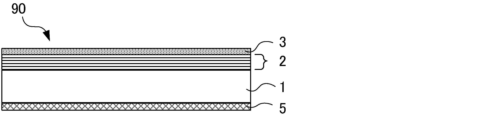
- FIG. 1 is a schematic cross-sectional view showing an example of a substrate 90 with a multilayer reflective film according to this embodiment.
- a substrate 90 with a multilayer reflective film of this embodiment includes a substrate 1 and a multilayer reflective film 2 provided on the substrate 1 .
- the multilayer reflective film 2 includes a multilayer film in which predetermined low refractive index layers and predetermined high refractive index layers are alternately laminated.
- a back surface conductive film 5 for an electrostatic chuck may be formed on the back surface of the substrate 1 (the surface opposite to the side on which the multilayer reflective film 2 is formed).
- the substrate 90 with a multilayer reflective film according to this embodiment will be specifically described.
- the substrate 1 preferably has a low coefficient of thermal expansion within the range of 0 ⁇ 5 ppb/° C. in order to prevent distortion of the transfer pattern due to heat during exposure to EUV light.
- a material having a low coefficient of thermal expansion within this range for example, SiO 2 —TiO 2 -based glass, multicomponent glass-ceramics, or the like can be used.
- the main surface (first main surface) of the substrate 1 on which the transfer pattern (absorber pattern 4a to be described later) is formed is preferably processed in order to increase the degree of flatness.
- the flatness is preferably 0.1 ⁇ m or less, more preferably 0.05 ⁇ m or less, and particularly preferably 0.05 ⁇ m or less in a 132 mm ⁇ 132 mm area of the main surface of the substrate 1 on which the transfer pattern is formed. It is preferably 0.03 ⁇ m or less.
- the second main surface (rear surface) opposite to the side on which the transfer pattern is formed is the surface fixed to the exposure device by an electrostatic chuck.
- the flatness is 0.1 ⁇ m or less, more preferably 0.05 ⁇ m or less, and particularly preferably 0.03 ⁇ m or less.
- the flatness is a value representing the warp (amount of deformation) of the surface indicated by TIR (Total Indicated Reading).
- TIR Total Indicated Reading
- the flatness (TIR) is measured by taking the surface of the substrate 1 as a reference and defining the plane determined by the method of least squares as the focal plane, and measuring the highest position of the surface of the substrate 1 above the focal plane and the substrate below the focal plane. It is the absolute value of the height difference with the lowest position of the surface of 1.
- the surface roughness of the main surface of the substrate 1 on which the transfer pattern is formed is preferably 0.1 nm or less in root-mean-square roughness (Rq).
- the surface roughness can be measured with an atomic force microscope.
- the substrate 1 preferably has high rigidity in order to prevent deformation of the thin film (multilayer reflective film 2, etc.) formed thereon due to film stress.
- those having a high Young's modulus of 65 GPa or more are preferred.
- low refractive index layers containing at least one selected from ruthenium (Ru) and rhodium (Rh) and high refractive index layers containing silicon (Si) are alternately laminated. Including multilayer film.
- the high refractive index layer is a layer containing silicon (Si).
- the high refractive index layer may contain Si alone or may contain a Si compound.
- the Si compound may contain Si and at least one element selected from the group consisting of B, C, N, O and H.
- the high refractive index layer is preferably made of silicon (Si). It should be noted that the phrase "the high refractive index layer is made of silicon (Si)" does not prevent impurities other than Si from being unavoidably mixed in the high refractive index layer. The same is true for other thin films and other elements.
- the low refractive index layer contains at least one selected from ruthenium (Ru) and rhodium (Rh).
- Ru ruthenium
- Rh rhodium
- the multilayer reflective film 2 includes a multilayer film in which low refractive index layers containing at least one selected from ruthenium (Ru) and rhodium (Rh) and high refractive index layers containing silicon (Si) are alternately laminated. As a result, the effective reflecting surface of the multilayer reflective film 2 can be made shallower than the conventional Mo/Si multilayer reflective film.
- Si in the high refractive index layer diffuses, which may cause a problem that the reflectance of the multilayer reflective film 2 to EUV light is lowered.
- the occurrence of this problem can be suppressed by including a predetermined additive element in addition to Ru and/or Rh in the low refractive index layer.
- the low refractive index layer of the substrate 90 with a multilayer reflective film of the present embodiment further contains an additive element having a work function in the range of more than 3.7 eV and less than 4.7 eV as a predetermined additive element.
- an additive element having a work function in the range of more than 3.7 eV and less than 4.7 eV as a predetermined additive element.
- the work function of Ru is 4.71 eV and the work function of Rh is 4.98 eV, so the work function of the additive element is lower than that of Ru. Therefore, by adding the additive element to the low refractive index layer, diffusion of the material (Si) of the high refractive index layer into the low refractive index layer can be suppressed.
- the high refractive index layer contains an element having a work function equal to or greater than that of Ru, there arises a problem that Si in the high refractive index layer diffuses into the low refractive index layer.
- the work function of Mg is 3.66 eV, the work function of the additive element is higher than that of Mg. If an element having a work function equal to or lower than that of Mg is added to the low refractive index layer, it becomes difficult to manufacture a pure metal target for deposition by sputtering. Therefore, the work function of the additive element must be within the range described above.
- the work function of an additive element means the work function of a metal composed of one kind of additive element, not an alloy.
- the additive element can also be selected based on the magnitude of the Fermi level of the metal. That is, the additive element contained in the low refractive index layer is a metal element having a Fermi level higher than that of Ru and lower than that of magnesium (Mg).
- Si which is the material of the high refractive index layer
- Si is known to have the property of diffusing easily into metal.
- the ease with which Si diffuses into metal depends on the work function of the metal. That is, when the work function of the metal of the low refractive index layer increases, Si diffuses easily into the metal (low refractive index layer). As a result, the reflectance of the EUV light by the multilayer reflective film 2 is lowered. A decrease in reflectance may occur particularly remarkably after the multilayer reflective film 2 is annealed. Conversely, when the work function of the metal becomes small, it becomes difficult for Si to diffuse into the metal (low refractive index layer). Therefore, the additive element contained in the low refractive index layer for forming the multilayer reflective film 2 in combination with the high refractive index layer containing Si is preferably a metal with a small work function.
- the additive element contained in the low refractive index layer for forming the multilayer reflective film 2 in combination with the high refractive index layer containing Si is preferably a metal with a small work function.
- the work function of Ru is smaller than 4.71 eV It can be understood that diffusion of Si into the low refractive index layer can be reduced in the case of the low refractive index layer containing an additive element having a work function. Also, it can be understood that the adhesion between the low refractive index layer and the high refractive index layer can be improved.
- the work function of Si is 4.61 eV (the difference between the vacuum level and the middle of the bandgap (Fermi level)).
- a low refractive index layer made of a material obtained by adding a predetermined additive element to Ru and/or Rh a high refractive index layer having a shallow effective reflection surface and containing Si can be changed from a high refractive index layer to a low refractive index layer. and the diffusion of Si atoms can be suppressed.
- the multilayer reflective film 2 of the substrate 90 with a multilayer reflective film can be prevented from lowering its reflectance for EUV light. Also, the adhesion between the low refractive index layer and the high refractive index layer of the multilayer reflective film 2 can be improved.
- Fig. 7 shows the relationship between the atomic number of the metal element and the work function.
- Elements inside the squares indicated by dashed lines in FIG. 7 are metal elements whose work functions are in the range of more than 3.7 eV and less than 4.7 eV.
- Table 2 shows a list of additive elements contained in the low refractive index layer of the multilayer reflective film 2 of the substrate 90 with the multilayer reflective film of this embodiment.
- Table 2 shows the work function, refractive index (n) and extinction coefficient (k) of each additive element.
- the additive element may be indicated as "X".
- the low refractive index layer is made of Ru and an additive element, the material of the low refractive index layer may be described as RuX.
- the low refractive index layer includes thallium (Tl), hafnium (Hf), titanium (Ti), zirconium (Zr), manganese (Mn), indium (In), gallium (Ga), and cadmium (Cd). , bismuth (Bi), tantalum (Ta), lead (Pb), silver (Ag), aluminum (Al), vanadium (V), niobium (Nb), tin (Sn), zinc (Zn), mercury (Hg) , chromium (Cr), iron (Fe), antimony (Sb), tungsten (W), molybdenum (Mo) and copper (Cu).
- the work functions of these additive elements are in the range of more than 3.7 eV and less than 4.7 eV. Therefore, the phenomenon that Si atoms diffuse from the high refractive index layer containing Si to the low refractive index layer can be suppressed, and the adhesion between the low refractive index layer and the high refractive index layer can be improved.
- the additive elements included in the anti-diffusion group A are additive elements having a work function of more than 3.7 eV and not more than 4.3 eV.
- the additive elements included in the diffusion prevention group B are additive elements having a work function higher than 4.3 eV and 4.5 eV or less.
- Additive elements included in diffusion-inhibiting group C are those with a work function higher than 4.5 eV and lower than 4.7 eV.
- the "diffusion prevention group" column in Table 2 shows the diffusion prevention group for each additive element.
- the additive elements belonging to diffusion prevention group A are Tl, Hf, Ti, Zr, Mn, In, Ga, Cd, Bi, Ta, Pb, Ag, Al, V, Nb and Sn.
- the additive elements belonging to the anti-diffusion group B are Zn, Hg, Cr and Fe.
- Additive elements belonging to diffusion prevention group C are Sb, W, Mo and Cu.
- the additive elements belonging to the anti-diffusion groups A, B and C can have a lower limit for the amount of addition of the low refractive index layer.
- the addition amount of the additive element of the diffusion prevention group A is preferably 1 atomic % or more, more preferably 3 atomic % or more.
- the addition amount of the additive element of the diffusion prevention group B is preferably 4 atomic % or more, more preferably 7 atomic % or more.
- the amount of the additive element added to the diffusion prevention group C is preferably 8 atomic % or more, more preferably 12 atomic % or more.
- the column of "lower limit (atomic %)" in Table 2 shows the diffusion prevention group of each additive element.
- the ratio of the content of the additive element of diffusion prevention group A to the content of the main material (Ru content, Rh content, or RuRh content) of the low refractive index layer is preferably 0.01 or more, more preferably 0.03 or more.
- the ratio of the content of the additive element of the diffusion prevention group B to the content of the main material of the low refractive index layer is preferably 0.04 or more, more preferably 0.08 or more.
- the ratio of the content of the additive element of the diffusion prevention group C to the content of the main material of the low refractive index layer is preferably 0.09 or more, more preferably 0.13 or more.
- the additive element is preferably an additive element belonging to anti-diffusion groups A and B, more preferably an additive element belonging to anti-diffusion group A. Further, a plurality of additive elements may be selected from diffusion prevention groups A, B and/or C.
- one high refractive index layer (Si) and a low refractive index layer 1 having a refractive index (n) of 0.88 or more and 0.96 or less and an extinction coefficient (k) of 0 or more and 0.08 or less A multilayer film was modeled by stacking 40 cycles of two layers stacked in this order as one cycle.
- the "reflectance for EUV light with a wavelength of 13.5 nm" means that the film thickness of the high refractive index layer is variable in the range of 0 nm or more and 6 nm or less, and the film thickness of the low refractive index layer is variable in the range of 0 nm or more and 6 nm or less. and the calculated maximum reflectance was used.
- the curve indicated by the dashed line shows the relationship between the refractive index (n) and the extinction coefficient (k).
- k 0.0021n -51.65 Expression (2) It is a curve showing that When the material of the low refractive index layer has a refractive index (n) and an extinction coefficient (k) on the dashed line of formula (2), the laminated structure of this low refractive index layer and the high refractive index layer of Si When the multilayer reflective film 2 is formed, the reflectance of the multilayer reflective film 2 for EUV light with a wavelength of 13.5 nm can be predicted to be 35% by simulation.
- one high refractive index layer (Si) and a low refractive index layer 1 having a refractive index (n) of 0.88 or more and 0.96 or less and an extinction coefficient (k) of 0 or more and 0.08 or less A multilayer film was modeled by stacking 40 cycles of two layers stacked in this order as one cycle.
- the "reflectance for EUV light with a wavelength of 13.5 nm" means that the film thickness of the high refractive index layer is variable in the range of 0 nm or more and 6 nm or less, and the film thickness of the low refractive index layer is variable in the range of 0 nm or more and 6 nm or less. and the calculated maximum reflectance was used.
- FIG. 8 shows the relationship between the refractive index (n) and the extinction coefficient (k) of each additive element.
- the reflectance for EUV light with a wavelength of 13.5 nm can be predicted from the values of the refractive index (n) and extinction coefficient (k) of the additive element.
- the multilayer reflective film 2 having a low refractive index layer of Mo and a high refractive index layer of Si from the values of the refractive index (n) and extinction coefficient (k) of Mo shown in FIG.
- the reflectance of the multilayer reflective film 2 for EUV light can be predicted.
- one cycle is composed of two layers, one high refractive index layer (Si) and one low refractive index layer, and the two layers are stacked in this order.
- the reflectance is the maximum reflectance predicted when the thickness of the high refractive index layer is variable in the range of 0 nm or more and 6 nm or less and the thickness of the low refractive index layer is variable in the range of 0 nm or more and 6 nm or less. is.
- FIG. 8 is a prediction when the number of layers of the multilayer reflective film 2 is 40, it can be said that the same tendency is observed even when the number of layers is less than 40, for example, about 35. .
- the additive elements can be divided into three optical property groups depending on the influence of the additive elements on the reflectance.
- the additive elements included in the optical property group a are additive elements with higher reflectance than the solid line (reflectance of 50%) of formula (1).
- the additive elements included in the optical property group b (shown as “Group b” in FIG. 8) have lower reflectance than the solid line (reflectance of 50%) in formula (1) and the dashed line in formula (2) ( It is an additive element with a higher reflectance than 35%).
- the additive elements included in the optical property group c (shown as “Group c” in FIG. 8) are additive elements with lower reflectance than the dashed line (reflectance of 35%) in formula (2).
- the column of "optical property group” in Table 2 shows the optical property group of each additive element.
- the amount of the additive element added to the low refractive index layer can have an upper limit. This is because the reflectance of the multilayer reflective film 2 decreases when the amount of the additive element added to the low refractive index layer is large.
- the amount of the additive element in the optical property group a is preferably 50 atomic % or less, more preferably 40 atomic % or less.
- the amount of the additive element in the optical property group b is preferably 30 atomic % or less, more preferably 20 atomic % or less.
- the amount of the additive element in the optical property group c is preferably 15 atomic % or less, more preferably 10 atomic % or less.
- the "upper limit (atomic %)" column in Table 2 shows the optical property group of each additive element.
- the ratio of the content of the additive element in the optical property group a to the content of the main material (Ru content, Rh content, or RuRh content) of the low refractive index layer (content of additive element/content of main material ) is preferably 0.56 or less, more preferably 0.44 or less.
- the ratio of the content of the additive element of the optical property group b to the content of the main material of the low refractive index layer is preferably 0.33 or less, more preferably 0.22 or less.
- the ratio of the content of the additive element of the optical property group c to the content of the main material of the low refractive index layer is preferably 0.17 or less, more preferably 0.11 or less.
- the additive elements belonging to optical property group a are zirconium (Zr), niobium (Nb), and molybdenum (Mo).
- the additive elements belonging to the optical property group b are thallium (Tl), titanium (Ti), manganese (Mn), indium (In), cadmium (Cd), tantalum (Ta), lead (Pb), silver (Ag), vanadium (V), mercury (Hg), chromium (Cr) and tungsten (W).
- the additive element is preferably an additive element belonging to optical property groups a and b, and more preferably an additive element belonging to optical property group a. Further, multiple additive elements may be selected from optical property groups a, b and/or c.
- the content of the main material is preferably more than 70 atomic % and less than 99 atomic %.
- the content of the main material is preferably more than 70 atomic % and less than 99 atomic %.
- Ga is the additive element
- the content of the main material is preferably more than 85 atomic % and less than 99 atomic %.
- Cd is the additive element
- the content of the main material is preferably more than 70 atomic % and less than 99 atomic %.
- Bi the additive element, the content of the main material is preferably more than 85 atomic % and less than 99 atomic %.
- the content of the main material is preferably more than 70 atomic % and less than 99 atomic %.
- Pb is the additive element
- the content of the main material is preferably more than 70 atomic % and less than 99 atomic %.
- Ag is the additive element
- the content of the main material is preferably more than 70 atomic % and less than 99 atomic %.
- Al is the additive element
- the content of the main material is preferably more than 85 atomic % and less than 99 atomic %.
- V is an additive element, the content of the main material is preferably more than 70 atomic % and less than 99 atomic %.
- the content of the main material is preferably more than 50 atomic % and less than 99 atomic %.
- Sn is the additive element
- the content of the main material is preferably more than 85 atomic % and less than 99 atomic %.
- Zn is the additive element
- the content of the main material is preferably more than 85 atomic % and less than 96 atomic %.
- Hg is the additive element
- the content of the main material is preferably more than 70 atomic % and less than 96 atomic %.
- Cr the additive element, the content of the main material is preferably more than 70 atomic % and less than 96 atomic %.
- the content of the main material is preferably more than 85 atomic % and less than 96 atomic %.
- Sb is the additive element
- the content of the main material is preferably more than 85 atomic % and less than 92 atomic %.
- W is the additive element
- the content of the main material is preferably more than 70 atomic % and less than 92 atomic %.
- Mo is the additive element
- the content of the main material is preferably more than 50 atomic % and less than 92 atomic %.
- Cu is the additive element, the content of the main material is preferably more than 85 atomic % and less than 92 atomic %.
- the appropriate blending of the alloying additive elements in the low refractive index layer is based on the appropriate content of each additive element and the amount of each element in the alloy. amount can be estimated.
- the low refractive index layer preferably does not contain elements other than the main materials Ru and Rh and the additive elements listed in Table 2. This is because when elements other than the main material and additive elements are contained, there is a high possibility that Si of the high refractive index layer will diffuse into the low refractive index layer. Therefore, the low refractive index layer preferably consists only of Ru and/or Rh and a predetermined additive element.
- the multilayer reflective film-coated substrate 90 of the present embodiment preferably has a laminated structure of less than 40 cycles when the laminated structure of the low refractive index layer and the high refractive index layer is defined as one cycle.
- the laminated structure of the multilayer reflective film 2 is more preferably 35 cycles or less, and even more preferably 30 cycles or less. Since the effective reflection surface of the multilayer reflective film 2 of this embodiment is shallow, an appropriate reflectance can be obtained with a smaller number of cycles than the conventional multilayer reflective film 2 . Therefore, the 3D effect can be suppressed by using the substrate 90 with a multilayer reflective film of this embodiment.
- the laminated structure preferably has 20 or more periods, more preferably 25 or more periods.
- the multilayer reflective film 2 When forming the multilayer reflective film 2, it is possible to first form a high refractive index layer on the surface of the substrate 1 and then form a low refractive index layer.
- the multilayer reflective film 2 has a laminated structure of a predetermined number of cycles on the substrate 1, with one cycle of a high refractive index layer and a low refractive index layer.
- the uppermost layer of the multilayer reflective film 2 is a low refractive index layer.
- the low refractive index layer constitutes the outermost surface of the multilayer reflective film 2, depending on the material constituting the low refractive index layer, it may be easily oxidized, and the reflectance of the reflective mask 200 is reduced. I have something to do.
- the multilayer reflective film 2 by further forming a high refractive index layer on the uppermost low refractive index layer.
- a Si layer made of Si may be formed on the uppermost low refractive index layer instead of the high refractive index layer.
- the multilayer reflective film 2 When forming the multilayer reflective film 2, it is possible to first form a low refractive index layer on the surface of the substrate 1 and then form a high and low refractive index layer.
- the multilayer reflective film 2 has a laminated structure with a predetermined number of cycles on the substrate 1, with each cycle having a low refractive index layer and a high refractive index layer.
- the uppermost layer is a high refractive index layer, so it may be left as it is.
- the top layer of the multilayer reflective film 2 is a high refractive index layer, it is preferable to form a protective film 3 described later on the multilayer reflective film 2 .
- the uppermost layer of the multilayer reflective film 2 can be the low refractive index layer.
- Ru has the function of protecting the multilayer reflective film 2 from dry etching and cleaning in the manufacturing process of the reflective mask 200, which will be described later.
- the uppermost low refractive index layer can also function as the protective film 3 .
- the structure of the multilayer reflective film 2 preferably includes a low refractive index layer containing Ru, and a high refractive index layer and a low refractive index layer containing Ru are laminated in this order from the substrate 1 side. Therefore, it is preferable to have a structure in which the uppermost layer is a low refractive index layer.
- the film thickness and composition of the uppermost low-refractive-index layer can be appropriately adjusted from the standpoint of dry etching resistance and cleaning resistance.
- the film thickness and composition of the uppermost low refractive index layer are preferably the same as those of the other low refractive index layers.
- the single reflectance of the multilayer reflective film 2 used in this embodiment is, for example, 65% or more.
- the upper limit of the reflectance of the multilayer reflective film 2 is, for example, 73%.
- the thickness and period of the layers included in the multilayer reflective film 2 can be selected so as to satisfy Bragg's law.
- the thickness of one period is preferably about 7 nm.
- the multilayer reflective film 2 can be formed by a known method.
- the multilayer reflective film 2 can be formed by, for example, an ion beam sputtering method, a magnetron sputtering method, a reactive sputtering method, or the like.
- the multilayer reflective film 2 is a RuNb/Si multilayer film in which Nb is an additive element of the low refractive index layer
- a RuNb film having a thickness of about 3 nm is formed on the substrate 1 by ion beam sputtering using a RuNb target. Form on top.
- a Si target using a Si target, a Si film having a thickness of about 4 nm is formed.
- the surface layer of the multilayer reflective film 2 opposite to the substrate 1 is a layer containing Si (Si film).
- the thickness of one period of the RuNb/Si film is preferably 7 nm.
- the multilayer reflective film-coated substrate 90 of the present embodiment preferably has a protective film 3 provided on the multilayer reflective film 2 .
- a protective film 3 is formed on the multilayer reflective film 2 or in contact with the surface of the multilayer reflective film 2 in order to protect the multilayer reflective film 2 from dry etching and cleaning in the manufacturing process of the reflective mask 200 to be described later. be able to.
- the protective film 3 also has a function of protecting the multilayer reflective film 2 during black defect correction of the transfer pattern (absorber pattern 4a) using an electron beam (EB).
- EB electron beam
- FIG. 2 shows the case where the protective film 3 is one layer.
- the protective film 3 can have a laminated structure of two layers.
- the protective film 3 has a laminated structure of three or more layers, the bottom layer and the top layer are made of, for example, a substance containing Ru, and a metal other than Ru or an alloy is placed between the bottom layer and the top layer. can be interposed.
- the protective film 3 is made of, for example, a material containing ruthenium as its main component.
- Materials containing ruthenium as a main component include Ru metal simple substance, Rh metal simple substance, Ru containing titanium (Ti), niobium (Nb), rhodium (Rh), molybdenum (Mo), zirconium (Zr), yttrium (Y), Ru alloys containing at least one metal selected from boron (B), lanthanum (La), cobalt (Co) and rhenium (Re), and materials containing nitrogen therein.
- the Ru content ratio of the Ru alloy used for the protective film 3 is 50 atomic % or more and less than 100 atomic %, preferably 80 atomic % or more and less than 100 atomic %, more preferably 95 atomic % or more and less than 100 atomic %.
- the protective film 3 has a mask cleaning resistance, an etching stopper function when the absorber film 4 is etched, and a function of preventing the multilayer reflective film 2 from changing with time while ensuring sufficient EUV light reflectance. It is possible to combine
- the protective film 3 preferably contains the same material as the low refractive index layer. Further, in the substrate 90 with a multilayer reflective film of the present embodiment, the protective film 3 contains at least one selected from ruthenium (Ru) and rhodium (Rh) and the same additive element (X) as the low refractive index layer. is more preferred.
- the low refractive index layer contains at least one selected from ruthenium (Ru) and rhodium (Rh), and the predetermined additive element X described above. Therefore, the protective film 3 also preferably contains the same material (RuX, RhX or RuRhX) as the low refractive index layer.
- the protection film 3 can be expected to function as a part of the multilayer reflective film 2 by including the same material as the low refractive index layer. Therefore, an improvement in the reflectance of the multilayer reflective film 2 can be expected.
- the protective film 3 can be formed more easily. More preferably, the protective film 3 is made of a material having the same element and the same composition ratio as the low refractive index layer.
- the film thickness of the protective film 3 is not particularly limited as long as it can function as the protective film 3 .
- the film thickness of the protective film 3 is preferably 1.0 nm to 8.0 nm, more preferably 1.5 nm to 6.0 nm.
- the film thickness of the protective film 3 is preferably the same film thickness as the low refractive index layer of the multilayer reflective film 2 .
- the protective film 3 is preferably formed in contact with the surface of the high refractive index layer of the multilayer reflective film 2 . As a result, the protective film 3 can function as part of the multilayer reflective film 2 .
- the uppermost layer of the multilayer reflective film 2 described above is a low refractive index layer
- this uppermost low refractive index layer can also serve as the protective film 3 .
- the low refractive index layer of this embodiment is a thin film made of ruthenium (Ru) and/or rhodium (Rh) and a predetermined additive element, it can function as the protective film 3 . Therefore, when manufacturing a reflective mask 200 (EUV mask) using the reflective mask blank 100 described later, damage to the surface of the multilayer reflective film 2 can be suppressed, so that the reflectance characteristics for EUV light can be improved. become good.
- a known film forming method can be adopted without particular limitation.
- Specific examples of the method for forming the protective film 3 include an ion beam sputtering method, a magnetron sputtering method, a reactive sputtering method, a chemical vapor deposition method (CVD), and a vacuum deposition method.
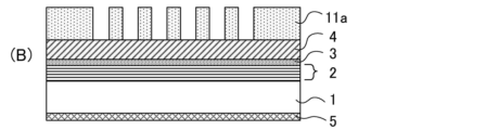
- the reflective mask blank 100 of this embodiment has an absorber film 4 on the multilayer reflective film 2 of the substrate 90 with the multilayer reflective film or on the protective film 3 formed on the multilayer reflective film 2 . Prepare.
- FIG. 3 is a schematic cross-sectional view showing an example of the reflective mask blank 100 of this embodiment.
- a reflective mask blank 100 shown in FIG. 3 has an absorber film 4 for absorbing EUV light on the multilayer reflective film 2 of the substrate 90 with a multilayer reflective film shown in FIG. Note that the reflective mask blank 100 can further have other thin films such as the resist film 11 on the absorber film 4 .
- the top layer of the multilayer reflective film 2 is preferably a low refractive index layer containing RuX or RuRhX.
- FIG. 4 is a schematic cross-sectional view showing an example of the reflective mask blank 100 of this embodiment.
- a reflective mask blank 100 shown in FIG. 4 has an absorber film 4 for absorbing EUV light on the protective film 3 of the substrate 90 with a multilayer reflective film shown in FIG. Note that the reflective mask blank 100 can further have other thin films such as the resist film 11 on the absorber film 4 .
- FIG. 5 is a schematic cross-sectional view showing another example of the reflective mask blank 100 of this embodiment.
- the reflective mask blank 100 can have an etch mask film 6 over the absorber film 4 .
- the reflective mask blank 100 can further have another thin film such as a resist film 11 on the etching mask film 6 .
- the absorber film 4 can absorb EUV light.
- EUV masks can be manufactured.
- the reflective mask blank 100 of the present embodiment it has a shallow effective reflective surface, and it is possible to suppress the diffusion of material atoms between the low-refractive-index layer and the high-refractive-index layer.
- a reflective mask blank 100 having a multilayer reflective film 2 can be obtained.
- the basic function of the absorber film 4 is to absorb EUV light.
- the absorber film 4 may be an absorber film 4 intended to absorb EUV light, or an absorber film 4 having a phase shift function in consideration of the phase difference of EUV light.
- the absorber film 4 having a phase shift function absorbs EUV light and reflects part of the EUV light to shift the phase. That is, in the reflective mask 200 patterned with the absorber film 4 having a phase shift function, the portion where the absorber film 4 is formed absorbs the EUV light and reduces the light to a level that does not adversely affect the pattern transfer. to reflect some light.
- the EUV light is reflected by the multilayer reflective film 2 (via the protective film 3 if there is one). Therefore, a desired phase difference is generated between the reflected light from the absorber film 4 having a phase shift function and the reflected light from the field portion.
- the absorber film 4 having a phase shift function is preferably formed so that the phase difference between the reflected light from the absorber film 4 and the reflected light from the multilayer reflective film 2 is 170 degrees to 260 degrees.
- the image contrast of the projected optical image is improved by the interference of the light beams with the inverted phase difference at the pattern edge portion. As the image contrast is improved, the resolution is increased, and various latitudes related to exposure such as exposure amount latitude and focus latitude can be increased.
- the absorber film 4 may be a single-layer film, or may be a multilayer film composed of a plurality of films (for example, a lower-layer absorber film and an upper-layer absorber film).
- a single-layer film the number of steps in manufacturing mask blanks can be reduced, improving production efficiency.
- the optical constant and film thickness thereof can be appropriately set so that the upper absorber film serves as an anti-reflection film during mask pattern defect inspection using light. This improves the inspection sensitivity when inspecting mask pattern defects using light.
- a film added with oxygen (O), nitrogen (N), etc. which improves oxidation resistance, is used as the upper absorber film, the stability over time is improved.
- the absorber film 4 By making the absorber film 4 a multilayer film in this way, it is possible to add various functions to the absorber film 4 .
- the absorber film 4 has a phase shift function, it is possible to widen the range of adjustment on the optical surface by making it a multilayer film, so it becomes easy to obtain a desired reflectance.
- the material of the absorber film 4 has a function of absorbing EUV light and can be processed by etching (preferably by dry etching with chlorine (Cl)-based gas and/or fluorine (F)-based gas). and is not particularly limited as long as the material has a high etching selectivity with respect to the protective film 3 .
- Compounds may include oxygen (O), nitrogen (N), carbon (C) and/or boron (B) in the above metals or alloys.
- the absorber film 4 can be formed by magnetron sputtering such as DC sputtering and RF sputtering.
- the absorber film 4 made of a tantalum compound or the like can be formed by a reactive sputtering method using a target containing tantalum and boron and using argon gas to which oxygen or nitrogen is added.
- the crystalline state of the absorber film 4 is preferably amorphous or microcrystalline. If the surface of the absorber film 4 is not smooth or flat, the edge roughness of the absorber pattern 4a increases, and the dimensional accuracy of the pattern may deteriorate.
- the surface roughness of the absorber film 4 is preferably 0.5 nm or less, more preferably 0.4 nm or less, still more preferably 0.3 nm or less in terms of root mean square roughness (Rms).
- the reflective mask blank 100 of this embodiment can have an etching mask film 6 on the absorber film 4 .
- a material of the etching mask film 6 it is preferable to use a material having a high etching selection ratio of the absorber film 4 to the etching mask film 6 (etching rate of the absorber film 4/etching rate of the etching mask film 6).
- the etching selection ratio of the absorber film 4 to the etching mask film 6 is preferably 1.5 or more, more preferably 3 or more.
- the reflective mask blank 100 of this embodiment preferably has an etching mask film 6 on the absorber film 4 .
- chromium or a chromium compound examples include materials containing Cr and at least one element selected from N, O, C and H.
- the etching mask film 6 more preferably contains CrN, CrO, CrC, CrON, CrOC, CrCN, or CrOCN, and is a CrO-based film (CrO film, CrON film, CrOC film, or CrOCN film) containing chromium and oxygen. is more preferred.
- the material for the etching mask film 6 it is preferable to use tantalum or a tantalum compound.
- tantalum compounds include materials containing Ta and at least one element selected from N, O, B and H. More preferably, the etching mask film 6 contains TaN, TaO, TaON, TaBN, TaBO or TaBON.
- the film thickness of the etching mask film 6 is preferably 3 nm or more in order to accurately form a pattern on the absorber film 4 . Moreover, the film thickness of the etching mask film 6 is preferably 15 nm or less in order to reduce the film thickness of the resist film 11 .
- a back surface conductive film 5 for electrostatic chuck can be formed on the back surface of the substrate 10 (the surface opposite to the side on which the multilayer reflective film 2 is formed).
- the sheet resistance required for the back surface conductive film 5 for electrostatic chucking is usually 100 ⁇ /square ( ⁇ /square) or less.
- the back conductive film 5 can be formed, for example, by magnetron sputtering or ion beam sputtering using a metal such as chromium or tantalum, or an alloy target thereof.
- the material of the back conductive film 5 is preferably a material containing chromium (Cr) or tantalum (Ta).
- the material of the back conductive film 5 is preferably a Cr compound containing Cr and at least one selected from boron, nitrogen, oxygen, and carbon.
- Cr compounds include CrN, CrON, CrCN, CrCON, CrBN, CrBON, CrBCN and CrBOCN.
- the material of the back conductive film 5 is preferably Ta (tantalum), an alloy containing Ta, or a Ta compound containing at least one of boron, nitrogen, oxygen, and carbon in any of these.
- Ta compounds include TaB, TaN, TaO, TaON, TaCON, TaBN, TaBO, TaBON, TaBCON, TaHf, TaHfO, TaHfN, TaHfON, TaHfCON, TaSi, TaSiO, TaSiN, TaSiON, and TaSiCON. can.
- the film thickness of the back surface conductive film 5 is not particularly limited as long as it functions as a film for an electrostatic chuck.
- the thickness of the back conductive film 5 is, for example, 10 nm to 200 nm.
- the reflective mask 200 of this embodiment includes an absorber pattern 4a obtained by patterning the absorber film 4 of the reflective mask blank 100 described above.
- FIG. 6A to 6D are schematic diagrams showing an example of a method for manufacturing the reflective mask 200.
- FIG. The reflective mask blank 100 of the present embodiment described above can be used to manufacture the reflective mask 200 of the present embodiment.
- An example of a method for manufacturing the reflective mask 200 will be described below.
- a substrate 1, a multilayer reflective film 2 formed on the substrate 1, a protective film 3 formed on the multilayer reflective film 2, and an absorber film 4 formed on the protective film 3 are provided.
- a reflective mask blank 100 is prepared.
- a resist film 11 is formed on the absorber film 4 to obtain a reflective mask blank 100 with the resist film 11 (FIG. 6A).
- a pattern is drawn on the resist film 11 by an electron beam drawing apparatus, and a resist pattern 11a is formed by developing and rinsing (FIG. 6B).
- etching gas for the absorber film 4 for example, a fluorine-based gas and/or a chlorine-based gas can be used.
- Fluorinated gases include CF4 , CHF3 , C2F6, C3F6, C4F6 , C4F8 , CH2F2 , CH3F , C3F8 , SF6 , and F2 . etc. can be used.
- Cl 2 , SiCl 4 , CHCl 3 , CCl 4 , BCl 3 and the like can be used as the chlorine-based gas.
- a mixed gas containing a fluorine-based gas and/or a chlorine-based gas and O 2 in a predetermined ratio can be used.
- These etching gases can optionally further contain inert gases such as He and/or Ar.
- the resist pattern 11a is removed with a resist remover.
- the reflective mask 200 of the present embodiment can be obtained through a wet cleaning process using an acidic or alkaline aqueous solution (FIG. 6D).
- a pattern (etching mask pattern) is formed on the etching mask film 6 using the resist pattern 11a as a mask. After that, a step of forming a pattern on the absorber film 4 using the etching mask pattern as a mask is added.
- the reflective mask 200 thus obtained has a structure in which a multilayer reflective film 2, a protective film 3, and an absorber pattern 4a are laminated on a substrate 1.
- the exposed area of the multilayer reflective film 2 (including the protective film 3) has the function of reflecting EUV light.
- the reflective mask 200 of this embodiment has a shallow effective reflective surface, and is a multilayer reflective film capable of suppressing the diffusion of material atoms between the low-refractive-index layer and the high-refractive-index layer. have Therefore, by using the reflective mask 200 of this embodiment, it is possible to transfer a finer pattern to the transfer target.
- the manufacturing method of the semiconductor device of this embodiment has a step of performing a lithography process using an exposure apparatus using the above-described reflective mask 200 to form a transfer pattern on a transfer target.
- a transfer pattern can be formed on a semiconductor substrate (transfer target) by lithography using the reflective mask 200 of this embodiment. This transfer pattern has a shape obtained by transferring the pattern of the reflective mask 200 .
- a semiconductor device can be manufactured by forming a transfer pattern on a semiconductor substrate using the reflective mask 200 .
- the multilayer reflective film 2 has a shallow effective reflective surface and can suppress the diffusion of material atoms between the low refractive index layer and the high refractive index layer.
- a semiconductor device can be manufactured using the reflective mask 200 . Therefore, by using the reflective mask 200 of this embodiment, the density and accuracy of the semiconductor device can be increased.
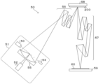
- FIG. 9 shows a schematic configuration of an EUV exposure apparatus 50, which is an apparatus for transferring a transfer pattern onto a resist film formed on a semiconductor substrate 60.
- an EUV light generator 51 an irradiation optical system 56, a reticle stage 58, a projection optical system 57, and a wafer stage 59 are precisely arranged along the optical path axis of EUV light.
- the container of the EUV exposure apparatus 50 is filled with hydrogen gas.
- the EUV light generation section 51 has a laser light source 52 , a tin droplet generation section 53 , a capture section 54 and a collector 55 .
- the tin droplets emitted from the tin droplet generator 53 are irradiated with a high-power carbon dioxide laser from the laser light source 52, the tin droplets are plasmatized to generate EUV light.
- the generated EUV light is collected by a collector 55 and made incident on a reflective mask 200 set on a reticle stage 58 via an irradiation optical system 56 .
- the EUV light generator 51 generates EUV light with a wavelength of 13.53 nm, for example.
- the EUV light reflected by the reflective mask 200 is normally reduced to about 1/4 of the pattern image light by the projection optical system 57 and projected onto the semiconductor substrate 60 (transferred substrate). Thereby, a given circuit pattern is transferred to the resist film on the semiconductor substrate 60 .
- a resist pattern can be formed on the semiconductor substrate 60 by developing the exposed resist film. By etching the semiconductor substrate 60 using the resist pattern as a mask, an integrated circuit pattern can be formed on the semiconductor substrate.
- a semiconductor device is manufactured through these processes and other necessary processes.
- a substrate 1 of 6025 size (approximately 152 mm ⁇ 152 mm ⁇ 6.35 mm) having polished first and second main surfaces was prepared.
- This substrate 1 is made of low thermal expansion glass (SiO 2 —TiO 2 based glass).
- the main surface of the substrate 1 was polished through a rough polishing process, a fine polishing process, a local polishing process, and a touch polishing process.
- a multilayer reflective film 2 composed of a Si high refractive index layer and a predetermined low refractive index layer was formed.
- Table 1 shows the materials and compositions of the low refractive index layers (RuX or RuRhX, where X is an additive element) of Examples 1 to 10.
- the material of the high refractive index layer in Examples 1-10 is Si.
- Table 1 shows the work function of the additive element (X) and the content (atomic %) of the additive element (X) in the low refractive index layer.
- the multilayer reflective film 2 was formed by ion beam sputtering using a Si target and a RuX target or RuRhX target (where X is an additive element) using Kr gas.
- a Si target is used to form a high refractive index layer of Si with a thickness of 4.2 nm so as to be in contact with the main surface of the substrate 1, followed by a RuX target or RuRhX target (where X is an additive element). was used to form a RuX or RuRhX low refractive index layer with a film thickness of 2.8 nm.
- the multilayer reflective film 2 was formed by laminating 35 periods (pairs) on the main surface of the substrate 1, with one period consisting of lamination of one high refractive index layer and one low refractive index layer.
- a RuRhNb film was formed as a protective film 3 on the multilayer reflective film 2 of Examples 1-10.
- the protective film 3 was formed with a thickness of 3.5 nm by magnetron sputtering in an Ar gas atmosphere using a RuRhNb target.
- the substrates 90 with multilayer reflective films of Examples 1 to 10 were manufactured.
- a substrate 90 with a multilayer reflective film was manufactured in the same manner as in Examples 1 to 10, except that the material of the low refractive index layer was Ru (Comparative Example 1) or RuRh (Comparative Example 2). Accordingly, the low refractive index layers of Comparative Examples 1 and 2 do not contain the additive element (X).
- a Ru target was used, and when forming the low refractive index layer of Comparative Example 2, a RuRh target was used.
- Table 1 shows the composition ratio (atomic %) of the low refractive index layers of Comparative Examples 1 and 2.
- the reflectance (R1, unit %) for EUV light (wavelength 13.5 nm) of the substrates 90 with multilayer reflective films of Examples and Comparative Examples was measured.
- the substrate 90 with the multilayer reflective film was heat-treated by heating at 200° C. for 10 minutes in an air atmosphere.
- the reflectance (R2, unit %) of the substrate 90 with the multilayer reflective film to EUV light was measured.
- the EUV due to the heat treatment of the substrate 90 with the multilayer reflective film A change in reflectance was obtained.
- Table 1 shows changes in EUV reflectance due to heat treatment.
- Example 7 the change in reflectance for EUV light before and after heat treatment at 200° C. for 10 minutes was 9.4% (Example 7) or less. was. Since the material of the low refractive index layer of the multilayer reflective film 2 of Examples 1 to 10 was RuX or RuRhX containing a predetermined additive element (X), diffusion of Si from the high refractive index layer to the low refractive index layer did not occur. Suppressed. Therefore, it is presumed that the change in reflectance was small before and after the heat treatment. In particular, the reflectance change of Example 1, in which the material of the low refractive index layer is RuNb, was as small as 6.9%.
- the reflectance of the substrates 90 with the multilayer reflective film with respect to EUV light changed significantly before and after the heat treatment at 200° C. for 10 minutes.
- Si diffused from the high refractive index layer to the low refractive index layer to form metal silicide (RuSi or RuRhSi) in the high refractive index layer, resulting in a large change in reflectance. It is speculated that
- the A reflective mask blank 100 was manufactured.
- a back conductive film 5 made of a CrN film was formed on the second main surface (back surface) of substrate 1 of substrate 90 with a multilayer reflective film by magnetron sputtering (reactive sputtering) under the following conditions.
- Conditions for forming the back conductive film 5 Cr target, mixed gas atmosphere of Ar and N2 (Ar: 90%, N: 10%), film thickness 20 nm.
- the reflective mask blanks 100 of Examples 1 to 10 were manufactured.
- Reflective mask 200 Next, using the reflective mask blanks 100 of Examples 1 to 10, reflective masks 200 were manufactured. The fabrication of the reflective mask 200 will be described with reference to FIGS. 6A through 6D.
- a resist film 11 was formed on the absorber film 4 of the reflective mask blank 100 .
- a desired pattern such as a circuit pattern was drawn (exposed) on the resist film 11, developed, and rinsed to form a predetermined resist pattern 11a (FIG. 6B).
- the absorber film 4 (TaBN film) was dry-etched using Cl 2 gas to form an absorber pattern 4a (FIG. 6C). After that, the resist pattern 11a was removed (FIG. 6D).
- the reflective masks 200 of Examples 1 to 10 were set on an EUV scanner, and EUV exposure was performed on a wafer in which a film to be processed and a resist film were formed on a semiconductor substrate 60 as a transfer target. Then, by developing the exposed resist film, a resist pattern was formed on the semiconductor substrate 56 on which the film to be processed was formed.
- the reflective mask 200 of Examples 1 to 10 has a shallow effective reflective surface, and is a multi-layer mask that can suppress the diffusion of material atoms between the low-refractive-index layer and the high-refractive-index layer. Since the reflective film 2 was provided, a fine and highly accurate transfer pattern (resist pattern) could be formed on the semiconductor substrate 60 (substrate to be transferred).
- This resist pattern is transferred to the film to be processed by etching, and various processes such as the formation of insulating films and conductive films, the introduction of dopants, and annealing are performed to manufacture semiconductor devices with desired characteristics at a high yield. We were able to.
Landscapes
- Physics & Mathematics (AREA)
- General Physics & Mathematics (AREA)
- Spectroscopy & Molecular Physics (AREA)
- Engineering & Computer Science (AREA)
- General Engineering & Computer Science (AREA)
- High Energy & Nuclear Physics (AREA)
- Exposure Of Semiconductors, Excluding Electron Or Ion Beam Exposure (AREA)
- Preparing Plates And Mask In Photomechanical Process (AREA)
Abstract
浅い実効反射面を有し、低屈折率層と、高屈折率層との間で材料となる原子が拡散するという現象を抑制することのできる多層反射膜を有する多層反射膜付き基板を提供する。 基板と、該基板の上に設けられた多層反射膜とを有する多層反射膜付き基板であって、前記多層反射膜は、ルテニウム(Ru)及びロジウム(Rh)から選ばれる少なくとも1つを含む低屈折率層と、ケイ素(Si)を含む高屈折率層とを交互に積層させた多層膜を含み、前記低屈折率層は、仕事関数が3.7eV超4.7eV未満の範囲にある添加元素を更に含むことを特徴とする多層反射膜付き基板である。
Description
本発明は、多層反射膜付き基板、反射型マスクブランク、反射型マスク、及び半導体装置の製造方法に関する。
近年における超LSIデバイスの高密度化、高精度化の更なる要求に伴い、極紫外(Extreme Ultra Violet、以下、EUVと称す。)光を用いた露光技術であるEUVリソグラフィが提案されている。
反射型マスクは、基板の上に形成された露光光を反射するための多層反射膜と、多層反射膜の上に形成され、露光光を吸収するためのパターン状の吸収体膜である吸収体パターンとを有する。多層反射膜により反射された光像が、反射光学系を通してシリコンウエハ等の半導体基板(被転写体)上に転写される。
反射型マスクを製造するための反射型マスクブランクの例として、特許文献1には、基板、前記基板上に積層された反射膜、前記反射膜上に積層された吸収膜を含むEUV用ブランクマスクが記載されている。特許文献1には、反射膜が、Ruで構成されるか、又は、RuにMo、Nb、Zrのうち一つ以上の元素が追加されたRu化合物で構成された第1層、及びSiで構成された第2層を含むペアが複数回積層された構造を有することが記載されている。
特許文献2には、互いに屈折率の異なるA、B、2種類の主材料の交互層よりなる多層薄膜構造を有する軟X線・真空紫外線用多層反射鏡が記載されている。特許文献2には、積層界面の荒れを小さくする作用を持つ副材料薄膜が、各A-B層間及び/又はB-A層間に少なくとも1層以上積層され、周期構造を形成していることが記載されている。特許文献2には、低屈折率層は一般にタングステン、モリブデン等の高融点金属材料又はそれらを主成分とした化合物で形成されること、高屈折率層は一般に炭素、シリコン、ホウ素、ベリリウム等の軽元素又はそれらを主成分とした化合物で形成されることが記載されている。更に、特許文献2には、副材料の例として、炭素C、ホウ素B、ベリリウムBe、炭化ケイ素SiC、窒化ケイ素Si3N4、酸化ケイ素SiO2、窒化ホウ素BN、炭化ホウ素B4C、窒化アルミニウムAlN等の原子番号13以下の軽元素の導体又はそれらの化合物が挙げられることが記載されている。
特許文献3には、ブラッグ回折効果を有する多層膜分光素子の重元素層と軽元素層との間に、SiとCからなる化合物中間層を使用したことを特徴とする多層膜分光反射鏡が記載されている。また、特許文献3には、重元素層としてMo、Ru、Rh、Reを用い、軽元素層にSiを用い、中間層にSi100-xCxを用いて多層膜を作製したことが記載されている。
特許文献4には、複数の物質層を周期的に積層した多層膜X線反射鏡が記載されている。特許文献4には、物質層の各層間に中間層を形成し、上記中間層として、少なくとも一つの上記物質層よりも融点の高い物質を使用することが記載されている。また、特許文献4には、重元素層としてMoを用い、軽元素層としてSiを用いてMo/Si多層膜を作製したことが記載されている。
非特許文献1には、Mo/Si多層反射膜(Mo/Si multilayer reflector)にB4C中間膜(interlayers)を用いることが記載されている。また、非特許文献1には、多層反射膜として、Ru/Si多層反射膜を用いることが記載されている。
Overt Wood et al. "Improved Ru/Si multilayer reflective coatings for advanced extreme-ultraviolet lithography photomasks". Proc. SPIE 9776, Extreme Ultraviolet (EUV) Lithography VII, 977619 (18 March 2016)
上述のEUVリソグラフィは、極紫外光(EUV光)を用いた露光技術である。EUV光とは、軟X線領域又は真空紫外線領域の波長帯の光であり、具体的には波長が0.2~100nm程度の光のことである。EUVリソグラフィの場合、波長13~14nm(例えば波長13.5nm)のEUV光を用いることができる。
EUVリソグラフィには、吸収体パターンを有する反射型マスクが用いられる。反射型マスクに照射されたEUV光は、吸収体パターンが存在する部分では吸収され、吸収体パターンが存在しない部分では反射される。吸収体パターンが存在しない部分には、多層反射膜が露出している。露出した多層反射膜がEUV光を反射する。EUVリソグラフィでは、多層反射膜(吸収体パターンが存在しない部分)により反射された光像が、反射光学系を通してシリコンウエハ等の半導体基板(被転写体)上に転写される。
多層反射膜としては、一般的に、屈折率の異なる元素が周期的に積層された多層膜が用いられる。例えば、波長13~14nm(例えば波長13.5nm)のEUV光に対する多層反射膜としては、低屈折率であるMo膜と、高屈折率であるSi膜を交互に40~60周期積層したMo/Si周期積層膜が用いられている。
反射型マスクを用いて半導体デバイスの高密度化、及び高精度化を達成するためには、反射型マスクにおける反射領域(多層反射膜の表面)が、露光光であるEUV光に対して高い反射率を有することが必要である。
半導体基板などの被転写体に転写されるノード(最小線幅)が狭くなるにつれ、転写特性に与える3D効果の影響が大きくなってきている。3D効果を抑制するためには吸収体パターンの膜厚を低減することが有効である。しかしながら、反射露光を用いるEUVリソグラフィでは、吸収体パターンを形成するための吸収体膜の薄膜化だけでは不十分である。そのため、EUV光が反射する反射面の制御も必要である。反射面の制御として、具体的には、多層反射膜の実効反射面をできるだけ表面に近づけて、多層反射膜から反射したEUV光が広がらないように制御することが必要である。本明細書では、多層反射膜の表面に比較的近い実効反射面のことを、「浅い実効反射面」という場合がある。多層反射膜が、浅い実効反射面を有することにより、3D効果を抑制することができ、多層反射膜の積層数を減らすことができる。
多層反射膜の実効反射面をできるだけ表面に近づけるためには、EUV光の反射率が高くなるように、多層反射膜の材料を選択する必要がある。多層反射膜は、低屈折率層と、高屈折率層との積層構造であることにより、EUV光を反射する。EUV光の反射率が高くなるように多層反射膜の材料を選択した場合、材料によっては、低屈折率層と、高屈折率層との間で材料となる原子が拡散するという現象が生じることがある。このような拡散現象が生じると、多層反射膜の反射率は低下してしまう。
そこで、本発明は、浅い実効反射面を有し、低屈折率層と、高屈折率層との間で材料となる原子が拡散するという現象を抑制することのできる多層反射膜を有する多層反射膜付き基板、反射型マスクブランク、及び反射型マスクを提供することを目的とする。また、本発明は、上記反射型マスクを用いた半導体装置の製造方法を提供することを目的とする。
上記課題を解決するため、本発明は以下の構成を有する。
(構成1)
本発明の構成1は、基板と、該基板の上に設けられた多層反射膜とを有する多層反射膜付き基板であって、
前記多層反射膜は、ルテニウム(Ru)及びロジウム(Rh)から選ばれる少なくとも1つを含む低屈折率層と、ケイ素(Si)を含む高屈折率層とを交互に積層させた多層膜を含み、
前記低屈折率層は、仕事関数が3.7eV超4.7eV未満の範囲にある添加元素を更に含むことを特徴とする多層反射膜付き基板である。
本発明の構成1は、基板と、該基板の上に設けられた多層反射膜とを有する多層反射膜付き基板であって、
前記多層反射膜は、ルテニウム(Ru)及びロジウム(Rh)から選ばれる少なくとも1つを含む低屈折率層と、ケイ素(Si)を含む高屈折率層とを交互に積層させた多層膜を含み、
前記低屈折率層は、仕事関数が3.7eV超4.7eV未満の範囲にある添加元素を更に含むことを特徴とする多層反射膜付き基板である。
(構成2)
本発明の構成2は、前記低屈折率層は、タリウム(Tl)、ハフニウム(Hf)、チタン(Ti)、ジルコニウム(Zr)、マンガン(Mn)、インジウム(In)、ガリウム(Ga)、カドミウム(Cd) 、ビスマス(Bi)、タンタル(Ta)、鉛(Pb)、銀(Ag)、アルミニウム(Al)、バナジウム(V)、ニオブ(Nb)、スズ(Sn)、亜鉛(Zn)、水銀(Hg)、クロム(Cr)、鉄(Fe)、アンチモン(Sb)、タングステン(W)、モリブデン(Mo)及び銅(Cu)から選択される少なくとも1つの添加元素を含むことを特徴とする構成1の多層反射膜付き基板である。
本発明の構成2は、前記低屈折率層は、タリウム(Tl)、ハフニウム(Hf)、チタン(Ti)、ジルコニウム(Zr)、マンガン(Mn)、インジウム(In)、ガリウム(Ga)、カドミウム(Cd) 、ビスマス(Bi)、タンタル(Ta)、鉛(Pb)、銀(Ag)、アルミニウム(Al)、バナジウム(V)、ニオブ(Nb)、スズ(Sn)、亜鉛(Zn)、水銀(Hg)、クロム(Cr)、鉄(Fe)、アンチモン(Sb)、タングステン(W)、モリブデン(Mo)及び銅(Cu)から選択される少なくとも1つの添加元素を含むことを特徴とする構成1の多層反射膜付き基板である。
(構成3)
本発明の構成3は、前記低屈折率層と前記高屈折率層との積層構造を1周期としたとき、積層構造が40周期未満であることを特徴とする構成1又は2の多層反射膜付き基板である。
本発明の構成3は、前記低屈折率層と前記高屈折率層との積層構造を1周期としたとき、積層構造が40周期未満であることを特徴とする構成1又は2の多層反射膜付き基板である。
(構成4)
本発明の構成4は、前記多層反射膜の上に保護膜を有する構成1乃至3の何れかの多層反射膜付き基板である。
本発明の構成4は、前記多層反射膜の上に保護膜を有する構成1乃至3の何れかの多層反射膜付き基板である。
(構成5)
本発明の構成5は、前記保護膜は、前記低屈折率層と同じ材料を含むことを特徴とする構成4の多層反射膜付き基板である。
本発明の構成5は、前記保護膜は、前記低屈折率層と同じ材料を含むことを特徴とする構成4の多層反射膜付き基板である。
(構成6)
本発明の構成6は、前記保護膜は、ルテニウム(Ru)及びロジウム(Rh)から選ばれる少なくとも1つと、前記低屈折率層と同じ添加元素とを含むことを特徴とする構成4又は5の多層反射膜付き基板である。
本発明の構成6は、前記保護膜は、ルテニウム(Ru)及びロジウム(Rh)から選ばれる少なくとも1つと、前記低屈折率層と同じ添加元素とを含むことを特徴とする構成4又は5の多層反射膜付き基板である。
(構成7)
本発明の構成7は、構成4乃至6の何れかの多層反射膜付き基板の前記保護膜の上に、吸収体膜を有することを特徴とする反射型マスクブランクである。
本発明の構成7は、構成4乃至6の何れかの多層反射膜付き基板の前記保護膜の上に、吸収体膜を有することを特徴とする反射型マスクブランクである。
(構成8)
本発明の構成8は、構成1乃至3の何れかの多層反射膜付き基板の前記多層反射膜の上に、吸収体膜を有することを特徴とする反射型マスクブランクである。
本発明の構成8は、構成1乃至3の何れかの多層反射膜付き基板の前記多層反射膜の上に、吸収体膜を有することを特徴とする反射型マスクブランクである。
(構成9)
本発明の構成9は、構成7又は8の反射型マスクブランクの前記吸収体膜をパターニングした吸収体パターンを有することを特徴とする反射型マスクである。
本発明の構成9は、構成7又は8の反射型マスクブランクの前記吸収体膜をパターニングした吸収体パターンを有することを特徴とする反射型マスクである。
(構成10)
本発明の構成10は、構成9の反射型マスクを用いて、露光装置を使用したリソグラフィプロセスを行い、被転写体に転写パターンを形成する工程を有することを特徴とする半導体装置の製造方法である。
本発明の構成10は、構成9の反射型マスクを用いて、露光装置を使用したリソグラフィプロセスを行い、被転写体に転写パターンを形成する工程を有することを特徴とする半導体装置の製造方法である。
本発明によれば、浅い実効反射面を有し、低屈折率層と、高屈折率層との間で材料となる原子が拡散するという現象を抑制することのできる多層反射膜を有する多層反射膜付き基板、反射型マスクブランク、及び反射型マスクを提供することができる。また、本発明によれば、上記反射型マスクを用いた半導体装置の製造方法を提供することができる。
以下、本発明の実施形態について、図面を参照しながら具体的に説明する。なお、以下の実施形態は、本発明を具体的に説明するための形態であって、本発明をその範囲内に限定するものではない。
図1は、本実施形態の多層反射膜付き基板90の一例を示す断面模式図である。本実施形態の多層反射膜付き基板90は、基板1と、基板1の上に設けられた多層反射膜2とを含む。多層反射膜2は、所定の低屈折率層と、所定の高屈折率層とを交互に積層させた多層膜を含む。基板1の裏面(多層反射膜2が形成された側と反対側の面)には、静電チャック用の裏面導電膜5が形成されてもよい。
図2は、本実施形態の多層反射膜付き基板90の別の一例を示す断面模式図である。図2に示す多層反射膜付き基板90は、基板1と、基板1の上に形成された多層反射膜2と、多層反射膜2の上に形成された保護膜3とを含む。基板1の裏面(多層反射膜2が形成された側と反対側の面)には、静電チャック用の裏面導電膜5が形成されてもよい。
本明細書において、「薄膜A(又は基板)の上に薄膜Bを配置(形成)する」とは、薄膜Bが、薄膜A(又は基板)の表面に接して配置(形成)されることを意味する場合の他、薄膜A(又は基板)と、薄膜Bとの間に他の薄膜Cを有することを意味する場合も含む。また、本明細書において、例えば「薄膜Bが薄膜A(又は基板)の表面に接して配置される」とは、薄膜A(又は基板)と薄膜Bとの間に他の薄膜を介さずに、薄膜A(又は基板)と薄膜Bとが直接、接するように配置されていることを意味する。また、本明細書において、「上に」とは、必ずしも鉛直方向における上側を意味するものではない。「上に」とは、薄膜及び基板などの相対的な位置関係を示しているに過ぎない。
本実施形態の多層反射膜付き基板90について、具体的に説明する。
<基板1>
基板1は、EUV光による露光時の熱による転写パターンの歪みを防止するため、0±5ppb/℃の範囲内の低熱膨張係数を有するものが好ましく用いられる。この範囲の低熱膨張係数を有する素材としては、例えば、SiO2-TiO2系ガラス、多成分系ガラスセラミックス等を用いることができる。
基板1は、EUV光による露光時の熱による転写パターンの歪みを防止するため、0±5ppb/℃の範囲内の低熱膨張係数を有するものが好ましく用いられる。この範囲の低熱膨張係数を有する素材としては、例えば、SiO2-TiO2系ガラス、多成分系ガラスセラミックス等を用いることができる。
基板1の転写パターン(後述の吸収体パターン4a)が形成される側の主表面(第1主表面)は、平坦度を高めるために加工されることが好ましい。基板1の主表面の平坦度を高めることによって、パターンの位置精度や転写精度を高めることができる。例えば、EUV露光の場合、基板1の転写パターンが形成される側の主表面の132mm×132mmの領域において、平坦度が0.1μm以下であることが好ましく、更に好ましくは0.05μm以下、特に好ましくは0.03μm以下である。また、転写パターンが形成される側と反対側の第2主表面(裏面)は、露光装置に静電チャックによって固定される表面である。裏面の142mm×142mmの領域において、平坦度が0.1μm以下、更に好ましくは0.05μm以下、特に好ましくは0.03μm以下である。なお、本明細書において平坦度は、TIR(Total Indicated Reading)で示される表面の反り(変形量)を表す値である。平坦度(TIR)は、基板1の表面を基準として最小二乗法で定められる平面を焦平面とし、この焦平面より上にある基板1の表面の最も高い位置と、焦平面より下にある基板1の表面の最も低い位置との高低差の絶対値である。
EUV露光の場合、基板1の転写パターンが形成される側の主表面の表面粗さは、二乗平均平方根粗さ(Rq)で0.1nm以下であることが好ましい。なお表面粗さは、原子間力顕微鏡で測定することができる。
基板1としては、その上に形成される薄膜(多層反射膜2など)の膜応力による変形を防止するために、高い剛性を有しているものが好ましい。特に、65GPa以上の高いヤング率を有しているものが好ましい。
<多層反射膜2>
多層反射膜2は、屈折率の異なる元素を主成分とする複数の層が周期的に積層された構成を有している。一般的に、多層反射膜2は、高屈折率材料である軽元素又はその化合物の薄膜(高屈折率層)と、低屈折率材料である重元素又はその化合物の薄膜(低屈折率層)とが交互に積層された多層膜を含む。
多層反射膜2は、屈折率の異なる元素を主成分とする複数の層が周期的に積層された構成を有している。一般的に、多層反射膜2は、高屈折率材料である軽元素又はその化合物の薄膜(高屈折率層)と、低屈折率材料である重元素又はその化合物の薄膜(低屈折率層)とが交互に積層された多層膜を含む。
多層反射膜2を形成するために、基板1側から高屈折率層と低屈折率層をこの順に複数周期積層することができる。この場合、1つの(高屈折率層/低屈折率層)の積層構造が、1周期となる。
本実施形態の多層反射膜2は、ルテニウム(Ru)及びロジウム(Rh)から選ばれる少なくとも1つを含む低屈折率層と、ケイ素(Si)を含む高屈折率層とを交互に積層させた多層膜を含む。
本実施形態において、高屈折率層は、ケイ素(Si)を含む層である。高屈折率層は、Si単体を含んでもよく、Si化合物を含んでもよい。Si化合物は、Siと、B、C、N、O及びHからなる群から選択される少なくとも1つの元素を含んでもよい。Siを含む層を高屈折率層として使用することによって、EUV光の反射率に優れた多層反射膜2が得られる。比較的高い反射率を得るために、高屈折率層は、ケイ素(Si)からなることが好ましい。なお、「高屈折率層がケイ素(Si)からなる」とは、不可避的に混入するSi以外の不純物が、高屈折率層中の存在することを妨げない。他の薄膜及び他の元素についても同様である。
本実施形態において、低屈折率層は、ルテニウム(Ru)及びロジウム(Rh)から選ばれる少なくとも1つを含む。低屈折率層がルテニウム(Ru)及び/又はロジウム(Rh)を含むことにより、従来のMo/Si多層反射膜と比較して、浅い実効反射面を得ることができる。
半導体基板のような被転写体に転写されるノード(最小線幅)が狭くなるにつれ、転写特性に与える3D効果の影響が大きくなってきている。3D効果とは、反射型マスク200の高さ方向の構造を含めた三次元的な構造が、マスクパターンに対する転写パターンの忠実度に影響を及ぼすことをいう。EUVリソグラフィにおいて、3D効果を抑制するためには、反射型マスク200の反射面の制御が必要である。反射面の制御として、具体的には、多層反射膜2の実効反射面をできるだけ表面に近づけることが必要である。反射型マスク200が浅い実効反射面を有することにより、多層反射膜2から反射したEUV光が広がらないように制御することができるので、3D効果を抑制することができる。多層反射膜2が、ルテニウム(Ru)及びロジウム(Rh)から選ばれる少なくとも1つを含む低屈折率層と、ケイ素(Si)を含む高屈折率層とを交互に積層させた多層膜を含むことにより、従来のMo/Si多層反射膜と比べて、多層反射膜2の実効反射面を浅くすることができる。
一方、Ru及び/又はRhを低屈折率層の材料として用いた場合、高屈折率層のSiが拡散して、多層反射膜2のEUV光に対する反射率が低下するという問題が生じることがある。本実施形態では、低屈折率層が、Ru及び/又はRhに加えて、所定の添加元素を更に含むことにより、この問題の発生を抑制することができる。
本実施形態の多層反射膜付き基板90の低屈折率層は、所定の添加元素として、仕事関数が3.7eV超4.7eV未満の範囲にある添加元素を更に含む。なお、Ruの仕事関数は4.71eVであり、Rhの仕事関数は4.98eVなので、添加元素の仕事関数は、Ruの仕事関数より低い。そのため、添加元素を低屈折率層に添加することにより、低屈折率層への高屈折率層の材料(Si)の拡散を抑制することができる。一方、高屈折率層が、Ruの仕事関数と同じか、それよりも大きな仕事関数を有する元素を含む場合には、高屈折率層のSiが低屈折率層に拡散するという問題が生じる。また、Mgの仕事関数は3.66eVなので、添加元素の仕事関数は、Mgの仕事関数より高い。Mgの仕事関数と同じか、それよりも低い仕事関数を有する元素を低屈折率層に添加した場合には、スパッタリングよる成膜のための純金属ターゲットの製造が困難になる。そのため、添加元素の仕事関数は、上述の範囲であることが必要である。添加元素の仕事関数とは、合金ではなく、1種類の添加元素からなる金属の仕事関数のことを意味する。
なお、仕事関数は、真空準位と、フェルミ準位との差であると考えられる。したがって、添加元素は、金属のフェルミ準位の大きさに基づいて選択することもできる。すなわち、低屈折率層に含まれる添加元素は、Ruのフェルミ準位よりも高く、かつマグネシウム(Mg)のフェルミ準位よりも低いフェルミ準位を有する金属元素である。
高屈折率層の材料であるケイ素(Si)は、金属中に拡散しやすい性質があることが知られている。金属中へのSiの拡散しやすさは、金属の仕事関数に依存する。すなわち、低屈折率層の金属の仕事関数が大きくなると、Siが金属(低屈折率層)の中に拡散しやすくなる。この結果、多層反射膜2によるEUV光の反射率は低下する。反射率の低下は、多層反射膜2のアニール後に、特に顕著に生じることがある。逆に、金属の仕事関数の小さくなると、Siが金属(低屈折率層)の中に拡散しにくくなる。したがって、Siを含む高屈折率層と組み合わせて多層反射膜2を形成するための低屈折率層に含まれる添加元素は、仕事関数が小さい金属であることが好ましい。
同様に、Si薄膜と、金属薄膜が接する場合、金属の仕事関数が大きくなると、Si薄膜と金属薄膜との密着性は低下する。逆に、金属の仕事関数が小さくなると、Si薄膜と金属薄膜との密着性は向上する。したがって、Siを含む高屈折率層と組み合わせて多層反射膜2を形成するための低屈折率層に含まれる添加元素は、仕事関数が小さい金属であることが好ましい。
上述のことから、Ruのみからなる低屈折率層、Rhのみからなる低屈折率層、及びRuRhのみからなる低屈折率層の場合と比べて、Ruの仕事関数である4.71eVよりも小さい仕事関数を有する添加元素を含む低屈折率層の場合には、低屈折率層へのSiの拡散を少なくすることができることが理解できる。また、低屈折率層と高屈折率層との密着性を向上させることができることが理解できる。
また、不純物のドーピングが無い真性半導体のSiの場合、Siの仕事関数は、4.61eV(真空準位と、バンドギャップのちょうど中間(フェルミ準位)との差)になる。添加元素として、Siの仕事関数よりも低い仕事関数を有する金属を用いることにより、低屈折率層へのSiの拡散を、より確実に抑制することができる。
上述のように、Ru及び/又はRhに所定の添加元素を加えた材料の低屈折率層を用いることにより、浅い実効反射面を有し、Siを含む高屈折率層から低屈折率層へとSi原子が拡散するという現象を抑制することができる。この結果、多層反射膜付き基板90の多層反射膜2の、EUV光に対する反射率の低下を抑制することができる。また、多層反射膜2の低屈折率層と、高屈折率層との密着性を向上させることができる。
図7に、金属元素の原子番号と、仕事関数との関係を示す。図7の破線で示す四角形の内側の元素は、仕事関数が3.7eV超4.7eV未満の範囲にある金属元素である。低屈折率層が、これらの金属元素を添加元素として含むことにより、Siを含む高屈折率層から低屈折率層へとSi原子が拡散するという現象を抑制し、低屈折率層と、高屈折率層との密着性を向上させることができる。
表2に、本実施形態の多層反射膜付き基板90の多層反射膜2の低屈折率層に含まれる添加元素の一覧表を示す。表2には、各添加元素の仕事関数、屈折率(n)及び消衰係数(k)を示す。なお、本明細書では、添加元素のことを「X」として示す場合がある。例えば、低屈折率層が、Ru及び添加元素を材料とする場合、低屈折率層の材料を、RuXと記載する場合がある。
本実施形態において、低屈折率層は、タリウム(Tl)、ハフニウム(Hf)、チタン(Ti)、ジルコニウム(Zr)、マンガン(Mn)、インジウム(In)、ガリウム(Ga)、カドミウム(Cd)、ビスマス(Bi)、タンタル(Ta)、鉛(Pb)、銀(Ag)、アルミニウム(Al)、バナジウム(V)、ニオブ(Nb)、スズ(Sn)、亜鉛(Zn)、水銀(Hg)、クロム(Cr)、鉄(Fe)、アンチモン(Sb)、タングステン(W)、モリブデン(Mo)及び銅(Cu)から選択される少なくとも1つの添加元素を含む。これらの添加元素の仕事関数は、3.7eV超4.7eV未満の範囲である。そのため、Siを含む高屈折率層から低屈折率層へとSi原子が拡散するという現象を抑制し、低屈折率層と、高屈折率層との密着性を向上させることができる。
仕事関数が低い添加元素の方が、低屈折率層へのSiの拡散をより少なくすることができる。そのため、添加元素を、仕事関数の大きさにより、3つの拡散防止グループに分けることができる。拡散防止グループAに含まれる添加元素は、仕事関数が3.7eV超4.3eV以下の添加元素である。拡散防止グループBに含まれる添加元素は、仕事関数が4.3eVより高く4.5eV以下の添加元素である。拡散防止グループCに含まれる添加元素は、仕事関数 4.5eVより高く4.7eV未満の添加元素である。表2の「拡散防止グループ」欄に、各添加元素の拡散防止グループを示す。
なお、拡散防止グループAに属する添加元素は、Tl、Hf、Ti、Zr、Mn、In、Ga、Cd、Bi、Ta、Pb、Ag、Al、V、Nb及びSnである。拡散防止グループBに属する添加元素は、Zn、Hg、Cr及びFeである。拡散防止グループCに属する添加元素は、Sb、W、Mo及びCuである。
低屈折率層に対する添加元素の添加量が少ない場合には、低屈折率層へのSiの拡散が起こりやすくなるため、多層反射膜2の反射率が低下する可能性がある。低屈折率層へのSiの拡散を抑制するために、拡散防止グループA、B及びCに属する添加元素は、低屈折率層の添加量の下限を有することができる。拡散防止グループAの添加元素の添加量は、1原子%以上であることが好ましく、3原子%以上とすることがより好ましい。拡散防止グループBの添加元素の添加量は、4原子%以上であることが好ましく、7原子%以上とすることがより好ましい。拡散防止グループCの添加量の添加元素は、8原子%以上であることが好ましく、12原子%以上とすることがより好ましい。表2の「下限(原子%)」欄に、各添加元素の拡散防止グループを示す。
また、低屈折率層の主材料の含有量(Ru含有量、Rh含有量又はRuRh含有量)に対する拡散防止グループAの添加元素の含有量の比率(添加元素の含有量/主材料の含有量)は、0.01以上であることが好ましく、0.03以上とすることがより好ましい。低屈折率層の主材料の含有量に対する拡散防止グループBの添加元素の含有量の比率は、0.04以上であることが好ましく、0.08以上とすることがより好ましい。低屈折率層の主材料の含有量に対する拡散防止グループCの添加元素の含有量の比率は、0.09以上であることが好ましく、0.13以上とすることがより好ましい。
低屈折率層へのSiの拡散を抑制するために、添加元素は、拡散防止グループA及びBに属する添加元素であることが好ましく、拡散防止グループAに属する添加元素であることがより好ましい。また、添加元素は、拡散防止グループA、B及び/又はCから複数選択してもよい。
図8に、添加元素の屈折率(n)と、消衰係数(k)との関係を示す。図8において、実線で示す曲線は、屈折率(n)と消衰係数(k)との関係が、
k=(1.735/n-1.716)2 ・・・式(1)
であることを示す曲線である。低屈折率層の材料が、式(1)の実線上の屈折率(n)及び消衰係数(k)である場合、この低屈折率層と、Siの高屈折率層との積層構造の多層反射膜2を形成したときに、多層反射膜2の波長13.5nmのEUV光に対する反射率は、シミュレーションにより50%であると予測できる。なお、シミュレーションでは、高屈折率層(Si)1層と、屈折率(n)が0.88以上0.96以下かつ消衰係数(k)が0以上0.08以下の低屈折率層1層とをこの順に積層した2層を1周期とし、それを40周期だけ積層させた多層膜をモデルとした。また、「波長13.5nmのEUV光に対する反射率」とは、上記シミュレーションにおいて、高屈折率層の膜厚を0nm以上6nm以下、低屈折率層の膜厚を0nm以上6nm以下の範囲で可変とし、計算された最大の反射率を用いた。
また、図8において、破線で示す曲線は、屈折率(n)と消衰係数(k)との関係が、
k=0.0021n-51.65 ・・・式(2)
であることを示す曲線である。低屈折率層の材料が、式(2)の破線上の屈折率(n)及び消衰係数(k)である場合、この低屈折率層と、Siの高屈折率層との積層構造の多層反射膜2を形成したときに、多層反射膜2の波長13.5nmのEUV光に対する反射率は、シミュレーションにより35%であると予測できる。なお、シミュレーションでは、高屈折率層(Si)1層と、屈折率(n)が0.88以上0.96以下かつ消衰係数(k)が0以上0.08以下の低屈折率層1層とをこの順に積層した2層を1周期とし、それを40周期だけ積層させた多層膜をモデルとした。また、「波長13.5nmのEUV光に対する反射率」とは、上記シミュレーションにおいて、高屈折率層の膜厚を0nm以上6nm以下、低屈折率層の膜厚を0nm以上6nm以下の範囲で可変とし、計算された最大の反射率を用いた。
図8には、各添加元素の屈折率(n)と消衰係数(k)との関係を示している。波長13.5nmのEUV光に対する反射率は、添加元素の屈折率(n)及び消衰係数(k)の値により、予測することができる。例えば、Moの低屈折率層と、Siの高屈折率層とを有する多層反射膜2の場合には、図8に示すMoの屈折率(n)及び消衰係数(k)の値から、EUV光に対する多層反射膜2の反射率を予測することができる。なお、この反射率を予測するためのモデルは、高屈折率層(Si)1層と、低屈折率層1層とをこの順に積層した2層を1周期とし、それを40周期だけ積層させた多層膜であり、反射率は、高屈折率層の膜厚を0nm以上6nm以下、低屈折率層の膜厚を0nm以上6nm以下の範囲で可変とし、予測された最大の反射率のことである。なお、図8は、多層反射膜2の積層数が40周期の時の場合の予測であるが、積層数が40周期未満、例えば35周期程度の場合であっても同様の傾向であるといえる。
図8に示す関係から、添加元素の反射率に与える影響により、添加元素を、3つの光学特性グループに分けることができる。光学特性グループa(図8に「Group a」として示す。)に含まれる添加元素は、反射率が式(1)の実線(反射率50%)よりも高い添加元素である。光学特性グループb(図8に「Group b」として示す。)に含まれる添加元素は、反射率が、式(1)の実線(反射率50%)よりも低く、式(2)の破線(反射率35%)よりも高い添加元素である。光学特性グループc(図8に「Group c」として示す。)に含まれる添加元素は、反射率が、式(2)の破線(反射率35%)よりも低い添加元素である。表2の「光学特性グループ」欄に、各添加元素の光学特性グループを示す。
EUV光に対する多層反射膜2の反射率を高く保つために、低屈折率層への添加元素の添加量は上限を有することができる。低屈折率層に対する添加元素の添加量が多い場合には、多層反射膜2の反射率が低下するためである。光学特性グループaの添加元素の添加量は、50原子%以下であることが好ましく、40原子%以下とすることがより好ましい。光学特性グループbの添加元素の添加量は、30原子%以下であることが好ましく、20原子%以下とすることがより好ましい。光学特性グループcの添加元素の添加量は、15原子%以下であることが好ましく、10原子%以下とすることがより好ましい。表2の「上限(原子%)」欄に、各添加元素の光学特性グループを示す。
また、低屈折率層の主材料の含有量(Ru含有量、Rh含有量又はRuRh含有量)に対する光学特性グループaの添加元素の含有量の比率(添加元素の含有量/主材料の含有量)は、0.56以下であることが好ましく、0.44以下とすることがより好ましい。低屈折率層の主材料の含有量に対する光学特性グループbの添加元素の含有量の比率は、0.33以下であることが好ましく、0.22以下とすることがより好ましい。低屈折率層の主材料の含有量に対する光学特性グループcの添加元素の含有量の比率は、0.17以下であることが好ましく、0.11以下とすることがより好ましい。
なお、光学特性グループaに属する添加元素は、ジルコニウム(Zr)、ニオブ(Nb)及びモリブデン(Mo)である。光学特性グループbに属する添加元素は、タリウム(Tl)、チタン(Ti)、マンガン(Mn)、インジウム(In)、カドミウム(Cd) 、タンタル(Ta)、鉛(Pb)、銀(Ag)、バナジウム(V)、水銀(Hg)、クロム(Cr)及びタングステン(W)である。光学特性グループcに属する添加元素は、ハフニウム(Hf)、ガリウム(Ga)、ビスマス(Bi)、アルミニウム(Al)、スズ(Sn)、亜鉛(Zn)、鉄(Fe)、アンチモン(Sb)及び銅(Cu)である。
良好な光学特性を得るために、添加元素は、光学特性グループa及びbに属する添加元素であることが好ましく、光学特性グループaに属する添加元素であることがより好ましい。また、添加元素は、光学特性グループa、b及び/又はcから複数選択してもよい。
以上述べたことから、低屈折率層中の添加元素の好ましい含有量の範囲は、表2に示す通りである。また、Tlが添加元素の場合の低屈折率層の主材料の含有量(Ru含有量、Rh含有量又はRuRh含有量)は、70原子%超99原子%未満であることが好ましい。Hfが添加元素の場合の主材料の含有量は、85原子%超99原子%未満であることが好ましい。Tiが添加元素の場合の主材料の含有量は、70原子%超99原子%未満であることが好ましい。Zrが添加元素の場合の主材料の含有量は、50原子%超99原子%未満であることが好ましい。Mnが添加元素の場合の主材料の含有量は、70原子%超99原子%未満であることが好ましい。Inが添加元素の場合の主材料の含有量は、70原子%超99原子%未満であることが好ましい。Gaが添加元素の場合の主材料の含有量は、85原子%超99原子%未満であることが好ましい。Cdが添加元素の場合の主材料の含有量は、70原子%超99原子%未満であることが好ましい。Biが添加元素の場合の主材料の含有量は、85原子%超99原子%未満であることが好ましい。Taが添加元素の場合の主材料の含有量は、70原子%超99原子%未満であることが好ましい。Pbが添加元素の場合の主材料の含有量は、70原子%超99原子%未満であることが好ましい。Agが添加元素の場合の主材料の含有量は、70原子%超99原子%未満であることが好ましい。Alが添加元素の場合の主材料の含有量は、85原子%超99原子%未満であることが好ましい。Vが添加元素の場合の主材料の含有量は、70原子%超99原子%未満であることが好ましい。Nbが添加元素の場合の主材料の含有量は、50原子%超99原子%未満であることが好ましい。Snが添加元素の場合の主材料の含有量は、85原子%超99原子%未満であることが好ましい。Znが添加元素の場合の主材料の含有量は、85原子%超96原子%未満であることが好ましい。Hgが添加元素の場合の主材料の含有量は、70原子%超96原子%未満であることが好ましい。Crが添加元素の場合の主材料の含有量は、70原子%超96原子%未満であることが好ましい。Feが添加元素の場合の主材料の含有量は、85原子%超96原子%未満であることが好ましい。Sbが添加元素の場合の主材料の含有量は、85原子%超92原子%未満であることが好ましい。Wが添加元素の場合の主材料の含有量は、70原子%超92原子%未満であることが好ましい。Moが添加元素の場合の主材料の含有量は、50原子%超92原子%未満であることが好ましい。Cuが添加元素の場合の主材料の含有量は、85原子%超92原子%未満であることが好ましい。
添加元素が複数の元素の合金の場合には、上述の各添加元素の適切な含有量、及び合金中の各元素の配合量に基づいて、低屈折率層中の合金添加元素の適切な配合量を推定することができる。なお、低屈折率層は、主材料であるRu及びRh、並びに表2に記載した添加元素以外の元素を含まないことが好ましい。主材料及び添加元素以外の元素を含む場合には、低屈折率層に、高屈折率層のSiが拡散する可能性が高くなるためである。したがって、低屈折率層は、Ru及び/又はRh、並びに所定の添加元素のみからなることが好ましい。
本実施形態の多層反射膜付き基板90は、低屈折率層と高屈折率層との積層構造を1周期としたとき、積層構造が40周期未満であることが好ましい。多層反射膜2の積層構造は、35周期以下であることがより好ましく、30周期以下であることが更に好ましい。本実施形態の多層反射膜2の実効反射面は浅いので、従来の多層反射膜2と比べて少ない周期数で適切な反射率を得ることができる。そのため、本実施形態の多層反射膜付き基板90を用いることにより、3D効果を抑制することができる。なお、多層反射膜2として適切な反射率を有するために、積層構造は、20周期以上であることが好ましく、25周期以上であることがより好ましい。
多層反射膜2の形成のときに、基板1の表面の上に、まず高屈折率層を形成し、次に低屈折率層を形成することができる。この場合、多層反射膜2は、基板1の上に高屈折率層及び低屈折率層を1周期として、所定の周期数の積層構造である。多層反射膜2の最上層は、低屈折率層である。この構造の多層反射膜2の場合、低屈折率層が多層反射膜2の最表面を構成すると低屈折率層を構成する材料によっては容易に酸化されてしまい反射型マスク200の反射率が減少することがある。そのため、最上層の低屈折率層上に高屈折率層を更に形成して多層反射膜2とすることが好ましい。最上層の低屈折率層上に、高屈折率層の代わりに、Siを材料とするSi層を形成することもできる。
多層反射膜2の形成のときに、基板1の表面の上に、まず低屈折率層を形成し、次に高低屈折率層を形成することができる。この場合、多層反射膜2は、基板1の上に低屈折率層及び高屈折率層を1周期として、所定の周期数の積層構造である。この構造の場合には、最上層が高屈折率層となるので、そのままでよい。
なお、上述のように、多層反射膜2の最上層が高屈折率層である場合には、多層反射膜2の上に、後述する保護膜3を形成することが好ましい。
一方、本実施形態の多層反射膜2の低屈折率層が、ルテニウム(Ru)を含む場合、多層反射膜2の最上層を低屈折率層とすることができる。Ruは、後述する反射型マスク200の製造工程におけるドライエッチング及び洗浄から多層反射膜2を保護するという機能を有するためである。この場合、最上層の低屈折率層は、保護膜3としての機能を兼ねることができる。
以上の述べたことから、多層反射膜2の構造は、低屈折率層がRuを含むことが好ましく、基板1側から高屈折率層と、Ruを含む低屈折率層とをこの順に積層して、最上層が低屈折率層となるような構造であることが好ましい。なお、最上層の低屈折率層の膜厚及び組成は、ドライエッチング耐性、及び洗浄耐性の点から、適宜調整することができる。ただし、高い反射率の多層反射膜2を得るためには、最上層の低屈折率層の膜厚及び組成は、他の低屈折率層の膜厚及び組成と同じであることが好ましい。
本実施形態に用いる多層反射膜2の単独での反射率は、例えば65%以上である。多層反射膜2の反射率の上限は、例えば73%である。なお、多層反射膜2に含まれる層の厚み及び周期は、ブラッグの法則を満たすように選択することができる。波長13.5nmのEUV光を反射するための多層反射膜2の場合には、1周期(高屈折率層及び低屈折率層の1ペア)の膜厚は、7nm程度であることが好ましい。
多層反射膜2は、公知の方法によって形成できる。多層反射膜2は、例えば、イオンビームスパッタリング法、マグネトロンスパッタリング法及び反応性スパッタリングなどにより形成できる。
例えば、多層反射膜2がNbを低屈折率層の添加元素としたRuNb/Si多層膜である場合、イオンビームスパッタリング法により、RuNbターゲットを用いて、厚さ3nm程度のRuNb膜を基板1の上に形成する。次に、Siターゲットを用いて、厚さ4nm程度のSi膜を形成する。このような操作を繰り返すことによって、RuNb/Si膜が20~39周期積層した多層反射膜2を形成することができる。このとき、多層反射膜2の基板1と反対側の表面層は、Siを含む層(Si膜)である。1周期のRuNb/Si膜の厚みは、7nmであることが好ましい。
<保護膜3>
図2に示すように、本実施形態の多層反射膜付き基板90は、多層反射膜2の上に設けられた保護膜3を有することが好ましい。
図2に示すように、本実施形態の多層反射膜付き基板90は、多層反射膜2の上に設けられた保護膜3を有することが好ましい。
後述する反射型マスク200の製造工程におけるドライエッチング及び洗浄から多層反射膜2を保護するために、多層反射膜2の上に、又は多層反射膜2の表面に接するように保護膜3を形成することができる。また、保護膜3は、電子線(EB)を用いた転写パターン(吸収体パターン4a)の黒欠陥修正の際に、多層反射膜2を保護する機能も有している。多層反射膜2の上に保護膜3が形成されることにより、反射型マスク200を製造する際の多層反射膜2の表面へのダメージを抑制することができる。その結果、多層反射膜2のEUV光に対する反射率特性が良好となる。
図2では、保護膜3が1層の場合を示している。しかしながら、保護膜3を2層の積層構造とすることができる。また、保護膜3を3層以上の積層構造とし、最下層及び最上層を、例えばRuを含有する物質からなる層とし、最下層と最上層との間に、Ru以外の金属、若しくは合金を介在させたものすることができる。保護膜3は、例えば、ルテニウムを主成分として含む材料により形成される。ルテニウムを主成分として含む材料としては、Ru金属単体、Rh金属単体、Ruにチタン(Ti)、ニオブ(Nb)、ロジウム(Rh)、モリブデン(Mo)、ジルコニウム(Zr)、イットリウム(Y)、ホウ素(B)、ランタン(La)、コバルト(Co)及びレニウム(Re)から選択される少なくとも1つの金属を含有したRu合金、及びそれらに窒素を含む材料が挙げられる。
保護膜3に用いるRu合金のRu含有比率は50原子%以上100原子%未満、好ましくは80原子%以上100原子%未満、より好ましくは95原子%以上100原子%未満である。この場合の保護膜3は、EUV光の反射率を十分確保しながら、マスク洗浄耐性、吸収体膜4をエッチング加工したときのエッチングストッパ機能、及び多層反射膜2の経時的変化防止の機能を兼ね備えることが可能となる。
本実施形態の多層反射膜付き基板90は、保護膜3は、低屈折率層と同じ材料を含むことが好ましい。また、本実施形態の多層反射膜付き基板90は、保護膜3は、ルテニウム(Ru)及びロジウム(Rh)から選ばれる少なくとも1つと、低屈折率層と同じ添加元素(X)とを含むことがより好ましい。
上述のように、低屈折率層は、ルテニウム(Ru)及びロジウム(Rh)から選ばれる少なくとも1つと、上述の所定の添加元素Xとを含む。そのため、保護膜3も、低屈折率層と同じ材料(RuX、RhX又はRuRhX)を含むことが好ましい。本実施形態の多層反射膜付き基板90において、保護膜3が、低屈折率層と同じ材料を含むことにより、多層反射膜2の一部としての機能を果たすことを期待できるようになる。そのため、多層反射膜2の反射率の向上を期待できる。また、低屈折率層と同じ材料を用いることにより、保護膜3をより容易に形成することができる。なお、保護膜3は、低屈折率層と同じ元素で同じ組成比の材料からなることがより好ましい。
保護膜3の膜厚は、保護膜3としての機能を果たすことができる限り特に制限されない。EUV光の反射率の観点から、保護膜3の膜厚は、好ましくは、1.0nmから8.0nm、より好ましくは、1.5nmから6.0nmである。
保護膜3が、低屈折率層と同じ組成の材料の場合には、保護膜3の膜厚は、多層反射膜2の低屈折率層の膜厚と同じ膜厚であることが好ましい。この場合、保護膜3は、多層反射膜2の高屈折率層の表面に接して形成されることが好ましい。この結果、保護膜3は、多層反射膜2の一部としての機能を有することができる。
上述の多層反射膜2の最上層が、低屈折率層である場合、この最上層の低屈折率層は、保護膜3を兼ねることができる。本実施形態の低屈折率層は、ルテニウム(Ru)及び/又はロジウム(Rh)、並びに所定の添加元素を材料とする薄膜なので、保護膜3としての機能を有することが可能である。そのため、後述する反射型マスクブランク100を用いて反射型マスク200(EUVマスク)を製造する際に、多層反射膜2の表面へのダメージを抑制することができるので、EUV光に対する反射率特性が良好となる。
保護膜3の形成方法としては、公知の膜形成方法を特に制限なく採用することができる。具体例としては、保護膜3の形成方法として、イオンビームスパッタリング法、マグネトロンスパッタリング法、反応性スパッタリング法、気相成長法(CVD)、及び真空蒸着法を挙げることができる。
<吸収体膜4>
本実施形態の反射型マスクブランク100は、上述の多層反射膜付き基板90の多層反射膜2の上に、又は多層反射膜2の上に形成された保護膜3の上に、吸収体膜4を備える。
本実施形態の反射型マスクブランク100は、上述の多層反射膜付き基板90の多層反射膜2の上に、又は多層反射膜2の上に形成された保護膜3の上に、吸収体膜4を備える。
図3は、本実施形態の反射型マスクブランク100の一例を示す断面模式図である。図3に示す反射型マスクブランク100は、図1に示す多層反射膜付き基板90の多層反射膜2の上に、EUV光を吸収するための吸収体膜4を有する。なお、反射型マスクブランク100は、吸収体膜4の上に、レジスト膜11などの他の薄膜を更に有することができる。図3に示す構造の場合、多層反射膜2の最上層は、RuX又はRuRhXを含む低屈折率層であることが好ましい。
図4は、本実施形態の反射型マスクブランク100の一例を示す断面模式図である。図4に示す反射型マスクブランク100は、図2に示す多層反射膜付き基板90の保護膜3の上に、EUV光を吸収するための吸収体膜4を有する。なお、反射型マスクブランク100は、吸収体膜4の上に、レジスト膜11などの他の薄膜を更に有することができる。
図5は、本実施形態の反射型マスクブランク100の別の例を示す断面模式図である。図5に示すように、反射型マスクブランク100は、吸収体膜4の上に、エッチングマスク膜6を有することができる。なお、反射型マスクブランク100は、エッチングマスク膜6の上に、レジスト膜11などの他の薄膜を更に有することができる。
本実施形態の反射型マスクブランク100では、吸収体膜4がEUV光を吸収することができるため、反射型マスクブランク100の吸収体膜4をパターニングすることによって、本発明の反射型マスク200(EUVマスク)を製造することができる。本実施形態の反射型マスクブランク100を用いることにより、浅い実効反射面を有し、低屈折率層と、高屈折率層との間で材料となる原子が拡散するという現象を抑制することのできる多層反射膜2を有する反射型マスクブランク100を得ることができる。
吸収体膜4の基本的な機能は、EUV光を吸収することである。吸収体膜4は、EUV光の吸収を目的とした吸収体膜4であってもよいし、EUV光の位相差も考慮した位相シフト機能を有する吸収体膜4であっても良い。位相シフト機能を有する吸収体膜4とは、EUV光を吸収するとともに、EUV光の一部を反射させて位相をシフトさせるものである。すなわち、位相シフト機能を有する吸収体膜4がパターニングされた反射型マスク200において、吸収体膜4が形成されている部分では、EUV光を吸収して減光しつつパターン転写に悪影響がないレベルで一部の光を反射させる。また、吸収体膜4が形成されていない領域(フィールド部)では、EUV光は、(保護膜3がある場合には保護膜3を介して)多層反射膜2で反射される。そのため、位相シフト機能を有する吸収体膜4からの反射光と、フィールド部からの反射光との間に所望の位相差が生ずる。位相シフト機能を有する吸収体膜4は、吸収体膜4からの反射光と、多層反射膜2からの反射光との位相差が170度から260度となるように形成されることが好ましい。反転した位相差の光同士がパターンエッジ部で干渉し合うことにより、投影光学像の像コントラストが向上する。その像コントラストの向上に伴って解像度が上がり、露光量裕度、及び焦点裕度等の露光に関する各種裕度を大きくすることができる。
吸収体膜4は単層の膜であってもよいし、複数の膜(例えば、下層吸収体膜及び上層吸収体膜)からなる多層膜であっても良い。単層膜の場合は、マスクブランク製造時の工程数を削減できて生産効率が向上する。多層膜の場合には、上層吸収体膜が、光を用いたマスクパターン欠陥検査時の反射防止膜になるように、その光学定数と膜厚を適当に設定することができる。このことにより、光を用いたマスクパターン欠陥検査時の検査感度が向上する。また、上層吸収体膜に酸化耐性が向上する酸素(O)及び窒素(N)等が添加された膜を用いると、経時安定性が向上する。このように、吸収体膜4を多層膜にすることによって、吸収体膜4に様々な機能を付加することが可能となる。吸収体膜4が位相シフト機能を有する場合には、多層膜にすることによって光学面での調整の範囲を大きくすることができるので、所望の反射率を得ることが容易になる。
吸収体膜4の材料としては、EUV光を吸収する機能を有し、エッチング等により加工が可能(好ましくは塩素(Cl)系ガス及び/又はフッ素(F)系ガスのドライエッチングでエッチング可能)であり、保護膜3に対してエッチング選択比が高い材料である限り、特に限定されない。そのような機能を有するものとして、パラジウム(Pd)、銀(Ag)、白金(Pt)、金(Au)、イリジウム(Ir)、タングステン(W)、クロム(Cr)、コバルト(Co)、マンガン(Mn)、スズ(Sn)、タンタル(Ta)、バナジウム(V)、ニッケル(Ni)、ハフニウム(Hf)、鉄(Fe)、銅(Cu)、テルル(Te)、亜鉛(Zn)、マグネシウム(Mg)、ゲルマニウム(Ge)、アルミニウム(Al)、ロジウム(Rh)、ルテニウム(Ru)、モリブデン(Mo)、ニオブ(Nb)、チタン(Ti)、ジルコニウム(Zr)、イットリウム(Y)、及びケイ素(Si)から選ばれる少なくとも1つの金属、2以上の金属を含む合金又はこれらの化合物を好ましく用いることができる。化合物は、上記金属又は合金に、酸素(O)、窒素(N)、炭素(C)及び/又はホウ素(B)を含んでもよい。
吸収体膜4は、DCスパッタリング法及びRFスパッタリング法などのマグネトロンスパッタリング法で形成することができる。例えば、タンタル化合物等の吸収体膜4は、タンタル及びホウ素を含むターゲットを用い、酸素又は窒素を添加したアルゴンガスを用いた反応性スパッタリング法により成膜することができる。
また、平滑性及び平坦性の点から、吸収体膜4の結晶状態は、アモルファス状又は微結晶の構造であることが好ましい。吸収体膜4の表面が平滑あるいは平坦でない場合、吸収体パターン4aのエッジラフネスが大きくなり、パターンの寸法精度が悪くなることがある。吸収体膜4の好ましい表面粗さは、二乗平均平方根粗さ(Rms)で、0.5nm以下であり、より好ましくは0.4nm以下、更に好ましくは0.3nm以下である。
<エッチングマスク膜6>
図5に示すように、本実施形態の反射型マスクブランク100は、吸収体膜4の上に、エッチングマスク膜6を有することができる。エッチングマスク膜6の材料としては、エッチングマスク膜6に対する吸収体膜4のエッチング選択比(吸収体膜4のエッチング速度/エッチングマスク膜6のエッチング速度)が高い材料を用いることが好ましい。エッチングマスク膜6に対する吸収体膜4のエッチング選択比は、1.5以上が好ましく、3以上が更に好ましい。
図5に示すように、本実施形態の反射型マスクブランク100は、吸収体膜4の上に、エッチングマスク膜6を有することができる。エッチングマスク膜6の材料としては、エッチングマスク膜6に対する吸収体膜4のエッチング選択比(吸収体膜4のエッチング速度/エッチングマスク膜6のエッチング速度)が高い材料を用いることが好ましい。エッチングマスク膜6に対する吸収体膜4のエッチング選択比は、1.5以上が好ましく、3以上が更に好ましい。
本実施形態の反射型マスクブランク100は、吸収体膜4の上に、エッチングマスク膜6を有することが好ましい。
エッチングマスク膜6の材料としては、クロム又はクロム化合物を使用することが好ましい。クロム化合物の例としては、Crと、N、O、C及びHから選ばれる少なくとも一つの元素とを含む材料が挙げられる。エッチングマスク膜6は、CrN、CrO、CrC、CrON、CrOC、CrCN又はCrOCNを含むことがより好ましく、クロム及び酸素を含むCrO系膜(CrO膜、CrON膜、CrOC膜又はCrOCN膜)であることが更に好ましい。
エッチングマスク膜6の材料としては、タンタル又はタンタル化合物を使用することが好ましい。タンタル化合物の例として、Taと、N、O、B及びHから選ばれる少なくとも一つの元素とを含む材料が挙げられる。エッチングマスク膜6は、TaN、TaO、TaON、TaBN、TaBO又はTaBONを含むことがより好ましい。
エッチングマスク膜6の材料としては、ケイ素又はケイ素化合物を使用することが好ましい。ケイ素化合物の例として、Siと、N、O、C及びHから選ばれる少なくとも一つの元素とを含む材料、並びにケイ素及びケイ素化合物に金属を含む金属ケイ素(金属シリサイド)、及び金属ケイ素化合物(金属シリサイド化合物)などが挙げられる。金属ケイ素化合物の例としては、金属と、Siと、N、O、C及びHから選ばれる少なくとも一つの元素とを含む材料が挙げられる。
エッチングマスク膜6の膜厚は、パターンを精度よく吸収体膜4に形成するために、3nm以上であることが好ましい。また、エッチングマスク膜6の膜厚は、レジスト膜11の膜厚を薄くするために、15nm以下であることが好ましい。
<裏面導電膜5>
基板10の裏面(多層反射膜2が形成された側と反対側の面)の上に、静電チャック用の裏面導電膜5を形成することができる。静電チャック用として、裏面導電膜5に求められるシート抵抗は、通常100Ω/□(Ω/square)以下である。裏面導電膜5は、例えば、クロム又はタンタル等の金属、又はそれらの合金のターゲットを使用したマグネトロンスパッタリング法又はイオンビームスパッタリング法によって形成することができる。裏面導電膜5の材料は、クロム(Cr)又はタンタル(Ta)を含む材料であることが好ましい。例えば、裏面導電膜5の材料は、Crに、ホウ素、窒素、酸素、及び炭素から選択される少なくとも一つを含有したCr化合物であることが好ましい。Cr化合物としては、例えば、CrN、CrON、CrCN、CrCON、CrBN、CrBON、CrBCN及びCrBOCNなどを挙げることができる。また、裏面導電膜5の材料は、Ta(タンタル)、Taを含有する合金、又はこれらのいずれかにホウ素、窒素、酸素、及び炭素の少なくとも一つを含有したTa化合物であることが好ましい。Ta化合物としては、例えば、TaB、TaN、TaO、TaON、TaCON、TaBN、TaBO、TaBON、TaBCON、TaHf、TaHfO、TaHfN、TaHfON、TaHfCON、TaSi、TaSiO、TaSiN、TaSiON、及びTaSiCONなどを挙げることができる。
基板10の裏面(多層反射膜2が形成された側と反対側の面)の上に、静電チャック用の裏面導電膜5を形成することができる。静電チャック用として、裏面導電膜5に求められるシート抵抗は、通常100Ω/□(Ω/square)以下である。裏面導電膜5は、例えば、クロム又はタンタル等の金属、又はそれらの合金のターゲットを使用したマグネトロンスパッタリング法又はイオンビームスパッタリング法によって形成することができる。裏面導電膜5の材料は、クロム(Cr)又はタンタル(Ta)を含む材料であることが好ましい。例えば、裏面導電膜5の材料は、Crに、ホウ素、窒素、酸素、及び炭素から選択される少なくとも一つを含有したCr化合物であることが好ましい。Cr化合物としては、例えば、CrN、CrON、CrCN、CrCON、CrBN、CrBON、CrBCN及びCrBOCNなどを挙げることができる。また、裏面導電膜5の材料は、Ta(タンタル)、Taを含有する合金、又はこれらのいずれかにホウ素、窒素、酸素、及び炭素の少なくとも一つを含有したTa化合物であることが好ましい。Ta化合物としては、例えば、TaB、TaN、TaO、TaON、TaCON、TaBN、TaBO、TaBON、TaBCON、TaHf、TaHfO、TaHfN、TaHfON、TaHfCON、TaSi、TaSiO、TaSiN、TaSiON、及びTaSiCONなどを挙げることができる。
裏面導電膜5の膜厚は、静電チャック用の膜として機能する限り特に限定されない。裏面導電膜5の膜厚は、例えば10nmから200nmである。
<反射型マスク200>
図6Dに示すように、本実施形態の反射型マスク200は、上述の反射型マスクブランク100の吸収体膜4をパターニングした吸収体パターン4aを備える。
図6Aから図6Dは、反射型マスク200の製造方法の一例を示す模式図である。上述の本実施形態の反射型マスクブランク100を使用して、本実施形態の反射型マスク200を製造することができる。以下、反射型マスク200の製造方法の例について説明する。
まず、基板1と、基板1の上に形成された多層反射膜2と、多層反射膜2の上に形成された保護膜3と、保護膜3の上に形成された吸収体膜4とを有する反射型マスクブランク100を準備する。次に、吸収体膜4の上に、レジスト膜11を形成して、レジスト膜11付きの反射型マスクブランク100を得る(図6A)。レジスト膜11に、電子線描画装置によってパターンを描画し、更に現像・リンス工程を経ることによって、レジストパターン11aを形成する(図6B)。
レジストパターン11aをマスクとして、吸収体膜4をドライエッチングする。これにより、吸収体膜4のレジストパターン11aによって被覆されていない部分がエッチングされ、吸収体パターン4aが形成される(図6C)。
吸収体膜4のエッチングガスとしては、例えば、フッ素系ガス及び/又は塩素系ガスを用いることができる。フッ素系ガスとしては、CF4、CHF3、C2F6、C3F6、C4F6、C4F8、CH2F2、CH3F、C3F8、SF6、及びF2等を用いることができる。塩素系ガスとしては、Cl2、SiCl4、CHCl3、CCl4、及びBCl3等を用いることができる。また、フッ素系ガス及び/又は塩素系ガスと、O2とを所定の割合で含む混合ガスを用いることができる。これらのエッチングガスは、必要に応じて、更に、He及び/又はArなどの不活性ガスを含むことができる。
吸収体パターン4aが形成された後、レジスト剥離液によりレジストパターン11aを除去する。レジストパターン11aを除去した後、酸性やアルカリ性の水溶液を用いたウェット洗浄工程を経ることによって、本実施形態の反射型マスク200を得ることができる(図6D)。
なお、吸収体膜4の上にエッチングマスク膜6が形成された反射型マスクブランク100を用いた場合には、レジストパターン11aをマスクとして用いてエッチングマスク膜6にパターン(エッチングマスクパターン)を形成した後、エッチングマスクパターンをマスクとして用いて吸収体膜4にパターンを形成する工程が追加される。
このようにして得られた反射型マスク200は、基板1の上に、多層反射膜2、保護膜3、及び吸収体パターン4aが積層された構造を有している。
多層反射膜2(保護膜3を含む)が露出している領域は、EUV光を反射する機能を有している。多層反射膜2(保護膜3を含む)が吸収体パターン4aによって覆われている領域は、EUV光を吸収する機能を有している。本実施形態の反射型マスク200は、浅い実効反射面を有し、低屈折率層と、高屈折率層との間で材料となる原子が拡散するという現象を抑制することのできる多層反射膜を有する。そのため、本実施形態の反射型マスク200を用いることにより、より微細なパターンを被転写体に転写することができる。
<半導体装置の製造方法>
本実施形態の半導体装置の製造方法は、上述の反射型マスク200を用いて、露光装置を使用したリソグラフィプロセスを行い、被転写体に転写パターンを形成する工程を有する。
本実施形態の半導体装置の製造方法は、上述の反射型マスク200を用いて、露光装置を使用したリソグラフィプロセスを行い、被転写体に転写パターンを形成する工程を有する。
本実施形態の反射型マスク200を使用したリソグラフィにより、半導体基板(被転写体)上に転写パターンを形成することができる。この転写パターンは、反射型マスク200のパターンが転写された形状を有している。半導体基板上に反射型マスク200によって転写パターンを形成することによって、半導体装置を製造することができる。
本実施形態によれば、浅い実効反射面を有し、低屈折率層と、高屈折率層との間で材料となる原子が拡散するという現象を抑制することのできる多層反射膜2を有する反射型マスク200を用いて、半導体装置を製造することができる。そのため、本実施形態の反射型マスク200を用いることにより、半導体装置を、高密度化、高精度化することができる。
図9を用いて、レジスト付き半導体基板60にEUV光によってパターンを転写する方法について説明する。
図9は、半導体基板60上に形成されているレジスト膜に転写パターンを転写するための装置であるEUV露光装置50の概略構成を示している。EUV露光装置50は、EUV光生成部51、照射光学系56、レチクルステージ58、投影光学系57及びウェハステージ59が、EUV光の光路軸に沿って精密に配置されている。EUV露光装置50の容器内には、水素ガスが充填されている。
EUV光生成部51は、レーザ光源52、錫液滴生成部53、捕捉部54、コレクタ55を有している。錫液滴生成部53から放出された錫液滴に、レーザ光源52からのハイパワーの炭酸ガスレーザが照射されると、液滴状態の錫がプラズマ化しEUV光が生成される。生成されたEUV光は、コレクタ55で集光され、照射光学系56を経てレチクルステージ58に設定された反射型マスク200に入射される。EUV光生成部51は、例えば、13.53nm波長のEUV光を生成する。
反射型マスク200で反射されたEUV光は、投影光学系57により通常1/4程度にパターン像光に縮小されて半導体基板60(被転写基板)上に投影される。これにより、半導体基板60上のレジスト膜に所与の回路パターンが転写される。露光されたレジスト膜を現像することによって、半導体基板60上にレジストパターンを形成することができる。レジストパターンをマスクとして半導体基板60をエッチングすることにより、半導体基板上に集積回路パターンを形成することができる。このような工程及びその他の必要な工程を経ることで、半導体装置が製造される。
以下、実施例及び比較例について図面を参照しつつ説明する。
(実施例1~10の多層反射膜付き基板90の作製)
まず、第1主表面及び第2主表面が研磨された6025サイズ(約152mm×152mm×6.35mm)の基板1を準備した。この基板1は、低熱膨張ガラス(SiO2-TiO2系ガラス)からなる基板1である。基板1の主表面は、粗研磨加工工程、精密研磨加工工程、局所加工工程、及びタッチ研磨加工工程によって研磨した。
まず、第1主表面及び第2主表面が研磨された6025サイズ(約152mm×152mm×6.35mm)の基板1を準備した。この基板1は、低熱膨張ガラス(SiO2-TiO2系ガラス)からなる基板1である。基板1の主表面は、粗研磨加工工程、精密研磨加工工程、局所加工工程、及びタッチ研磨加工工程によって研磨した。
次に、基板1の主表面(第1主表面)上に、Siの高屈折率層及び所定の低屈折率層からなる多層反射膜2を形成した。表1に、実施例1~10の低屈折率層(RuX又はRuRhX、Xは添加元素)の材料及び組成を示す。実施例1~10の高屈折率層の材料はSiである。表1には、添加元素(X)の仕事関数、及び低屈折率層中の添加元素(X)の含有量(原子%)を示す。
多層反射膜2は、Siターゲットと、RuXターゲット又はRuRhXターゲット(Xは添加元素)とを使用し、Krガスを用いてイオンビームスパッタリング法により、形成した。まず、基板1の主表面に接するように、Siターゲットを用いて、Siの高屈折率層を4.2nmの膜厚で成膜し、続いて、RuXターゲット又はRuRhXターゲット(Xは添加元素)を用いて、RuX又はRuRhXの低屈折率層を2.8nmの膜厚で成膜した。多層反射膜2は、1つの高屈折率層及び1つの低屈折率層の積層を1周期として、基板1の主表面に35周期(ペア)積層することにより形成した。
次に、実施例1~10の多層反射膜2の上に、保護膜3としてRuRhNb膜を形成した。保護膜3は、RuRhNbターゲットを使用し、Arガス雰囲気中で、マグネトロンスパッタリング法によって3.5nmの厚みで形成した。保護膜3の組成比(原子%)は、Ru:Rh:Nb=64:16:20である。
以上のようにして、実施例1~10の多層反射膜付き基板90を製造した。
(比較例1及び2の多層反射膜付き基板90の作製)
低屈折率層の材料をRu(比較例1)又はRuRh(比較例2)とした以外は、実施例1~10と同様にして、多層反射膜付き基板90を製造した。したがって、比較例1及び2の低屈折率層は、添加元素(X)を含まない。なお、比較例1の低屈折率層を形成する際には、Ruターゲットを用い、比較例2の低屈折率層を形成する際には、RuRhターゲットを用いた。表1に、比較例1及び2の低屈折率層の組成比(原子%)を示す。
低屈折率層の材料をRu(比較例1)又はRuRh(比較例2)とした以外は、実施例1~10と同様にして、多層反射膜付き基板90を製造した。したがって、比較例1及び2の低屈折率層は、添加元素(X)を含まない。なお、比較例1の低屈折率層を形成する際には、Ruターゲットを用い、比較例2の低屈折率層を形成する際には、RuRhターゲットを用いた。表1に、比較例1及び2の低屈折率層の組成比(原子%)を示す。
(多層反射膜付き基板90の反射率の評価)
上述のように作製した実施例及び比較例の多層反射膜付き基板90を用いて、多層反射膜付き基板90に対する熱処理による反射率の変化を測定した。
上述のように作製した実施例及び比較例の多層反射膜付き基板90を用いて、多層反射膜付き基板90に対する熱処理による反射率の変化を測定した。
具体的には、まず、実施例及び比較例の多層反射膜付き基板90のEUV光(波長13.5nm)に対する反射率(R1、単位%)を測定した。次に、多層反射膜付き基板90を、大気雰囲気中、200℃で、10分間加熱することにより熱処理をした。多層反射膜付き基板90を熱処理した後、多層反射膜付き基板90のEUV光に対する反射率(R2、単位%)を測定した。熱処理前の多層反射膜付き基板90の反射率(R1)の値から熱処理後の多層反射膜付き基板90の反射率(R2)の値を差し引くことによって、多層反射膜付き基板90の熱処理によるEUV反射率の変化を得た。表1に、熱処理によるEUV反射率の変化を示す。
表1に示すように、実施例1~10の多層反射膜付き基板90では、200℃、10分間の熱処理の前後において、EUV光に対する反射率の変化は9.4%(実施例7)以下だった。実施例1~10の多層反射膜2の低屈折率層の材料は、所定の添加元素(X)を含むRuX又はRuRhXであったため、高屈折率層から低屈折率層へのSiの拡散が抑制された。そのため、熱処理の前後において反射率の変化が小さかったものと推察される。特に、低屈折率層の材料がRuNbである実施例1の反射率の変化は6.9%と小さかった。
一方、比較例1及び2の多層反射膜付き基板90では、200℃、10分間の熱処理の前後において、EUV光に対する多層反射膜付き基板90の反射率が大きく変化した。比較例1及び2では、高屈折率層から低屈折率層へSiが拡散して、高屈折率層中で金属シリサイド(RuSi又はRuRhSi)が形成されたことにより、反射率が大きく変化したものと推察される。
(反射型マスクブランク100)
次に、実施例1~10の反射型マスクブランク100について説明する。
次に、実施例1~10の反射型マスクブランク100について説明する。
上述のようにして製造した多層反射膜付き基板90の基板1の裏面に裏面導電膜5を形成し、保護膜3の上に、吸収体膜4を形成することにより、実施例1~10の反射型マスクブランク100を製造した。
まず、多層反射膜付き基板90の基板1の第2主表面(裏面)に、CrN膜からなる裏面導電膜5をマグネトロンスパッタリング(反応性スパッタリング)法により下記の条件にて形成した。
裏面導電膜5の形成条件:Crターゲット、ArとN2の混合ガス雰囲気(Ar:90%、N:10%)、膜厚20nm。
裏面導電膜5の形成条件:Crターゲット、ArとN2の混合ガス雰囲気(Ar:90%、N:10%)、膜厚20nm。
次に、多層反射膜付き基板90の保護膜3の上に、吸収体膜4として膜厚55nmのTaBN膜を形成した。吸収体膜4の組成は、Ta:B:N=75:12:13(原子比)であり、膜厚は55nmであった。
以上のようにして、実施例1~10の反射型マスクブランク100を製造した。
(反射型マスク200)
次に、実施例1~10の反射型マスクブランク100を用いて、反射型マスク200を製造した。図6Aから図6Dを参照して反射型マスク200の製造を説明する。
次に、実施例1~10の反射型マスクブランク100を用いて、反射型マスク200を製造した。図6Aから図6Dを参照して反射型マスク200の製造を説明する。
まず、図6Aに示すように、反射型マスクブランク100の吸収体膜4の上に、レジスト膜11を形成した。そして、このレジスト膜11に回路パターン等の所望のパターンを描画(露光)し、更に現像、リンスすることによって所定のレジストパターン11aを形成した(図6B)。次に、レジストパターン11aをマスクにして吸収体膜4(TaBN膜)を、Cl2ガスを用いてドライエッチングすることで、吸収体パターン4aを形成した(図6C)。その後、レジストパターン11aを除去した(図6D)。
最後に純水(DIW)を用いたウェット洗浄を行って、実施例1~10の反射型マスク200を製造した。
(半導体装置の製造)
実施例1~10の反射型マスク200をEUVスキャナにセットし、被転写体である半導体基板60の上に被加工膜とレジスト膜が形成されたウエハに対してEUV露光を行った。そして、この露光済レジスト膜を現像することによって、被加工膜が形成された半導体基板56の上にレジストパターンを形成した。
実施例1~10の反射型マスク200をEUVスキャナにセットし、被転写体である半導体基板60の上に被加工膜とレジスト膜が形成されたウエハに対してEUV露光を行った。そして、この露光済レジスト膜を現像することによって、被加工膜が形成された半導体基板56の上にレジストパターンを形成した。
実施例1~10の反射型マスク200は、浅い実効反射面を有し、低屈折率層と、高屈折率層との間で材料となる原子が拡散するという現象を抑制することのできる多層反射膜2を有するので、半導体基板60(被転写基板)の上に微細かつ高精度の転写パターン(レジストパターン)を形成することができた。
このレジストパターンをエッチングにより被加工膜に転写し、また、絶縁膜、導電膜の形成、ドーパントの導入、あるいはアニールなど種々の工程を経ることで、所望の特性を有する半導体装置を高い歩留まりで製造することができた。


1 基板
2 多層反射膜
3 保護膜
4 吸収体膜
4a 吸収体パターン
5 裏面導電膜
6 エッチングマスク膜
11 レジスト膜
11a レジストパターン
50 EUV露光装置
51 EUV光生成部
52 レーザ光源
53 錫液滴生成部
54 捕捉部
55 コレクタ
56 照射光学系
57 投影光学系
58 レチクルステージ
59 ウェハステージ
60 半導体基板
90 多層反射膜付き基板
100 反射型マスクブランク
200 反射型マスク
2 多層反射膜
3 保護膜
4 吸収体膜
4a 吸収体パターン
5 裏面導電膜
6 エッチングマスク膜
11 レジスト膜
11a レジストパターン
50 EUV露光装置
51 EUV光生成部
52 レーザ光源
53 錫液滴生成部
54 捕捉部
55 コレクタ
56 照射光学系
57 投影光学系
58 レチクルステージ
59 ウェハステージ
60 半導体基板
90 多層反射膜付き基板
100 反射型マスクブランク
200 反射型マスク
Claims (10)
- 基板と、該基板の上に設けられた多層反射膜とを有する多層反射膜付き基板であって、
前記多層反射膜は、ルテニウム(Ru)及びロジウム(Rh)から選ばれる少なくとも1つを含む低屈折率層と、ケイ素(Si)を含む高屈折率層とを交互に積層させた多層膜を含み、
前記低屈折率層は、仕事関数が3.7eV超4.7eV未満の範囲にある添加元素を更に含むことを特徴とする多層反射膜付き基板。 - 前記低屈折率層は、タリウム(Tl)、ハフニウム(Hf)、チタン(Ti)、ジルコニウム(Zr)、マンガン(Mn)、インジウム(In)、ガリウム(Ga)、カドミウム(Cd)、ビスマス(Bi)、タンタル(Ta)、鉛(Pb)、銀(Ag)、アルミニウム(Al)、バナジウム(V)、ニオブ(Nb)、スズ(Sn)、亜鉛(Zn)、水銀(Hg)、クロム(Cr)、鉄(Fe)、アンチモン(Sb)、タングステン(W)、モリブデン(Mo)及び銅(Cu)から選択される少なくとも1つの添加元素を含むことを特徴とする請求項1に記載の多層反射膜付き基板。
- 前記低屈折率層と前記高屈折率層との積層構造を1周期としたとき、積層構造が40周期未満であることを特徴とする請求項1又は2に記載の多層反射膜付き基板。
- 前記多層反射膜の上に保護膜を有する請求項1乃至3の何れか1項に記載の多層反射膜付き基板。
- 前記保護膜は、前記低屈折率層と同じ材料を含むことを特徴とする請求項4に記載の多層反射膜付き基板。
- 前記保護膜は、ルテニウム(Ru)及びロジウム(Rh)から選ばれる少なくとも1つと、前記低屈折率層と同じ添加元素とを含むことを特徴とする請求項4又は5に記載の多層反射膜付き基板。
- 請求項4乃至6の何れか1項に記載の多層反射膜付き基板の前記保護膜の上に、吸収体膜を有することを特徴とする反射型マスクブランク。
- 請求項1乃至3の何れか1項に記載の多層反射膜付き基板の前記多層反射膜の上に、吸収体膜を有することを特徴とする反射型マスクブランク。
- 請求項7又は8に記載の反射型マスクブランクの前記吸収体膜をパターニングした吸収体パターンを有することを特徴とする反射型マスク。
- 請求項9に記載の反射型マスクを用いて、露光装置を使用したリソグラフィプロセスを行い、被転写体に転写パターンを形成する工程を有することを特徴とする半導体装置の製造方法。
Priority Applications (2)
| Application Number | Priority Date | Filing Date | Title |
|---|---|---|---|
| JP2023546920A JPWO2023037980A1 (ja) | 2021-09-07 | 2022-09-02 | |
| KR1020247003753A KR20240055724A (ko) | 2021-09-07 | 2022-09-02 | 다층 반사막 구비 기판, 반사형 마스크 블랭크, 반사형 마스크 및 반도체 장치의 제조 방법 |
Applications Claiming Priority (2)
| Application Number | Priority Date | Filing Date | Title |
|---|---|---|---|
| JP2021145749 | 2021-09-07 | ||
| JP2021-145749 | 2021-09-07 |
Publications (1)
| Publication Number | Publication Date |
|---|---|
| WO2023037980A1 true WO2023037980A1 (ja) | 2023-03-16 |
Family
ID=85507564
Family Applications (1)
| Application Number | Title | Priority Date | Filing Date |
|---|---|---|---|
| PCT/JP2022/033127 WO2023037980A1 (ja) | 2021-09-07 | 2022-09-02 | 多層反射膜付き基板、反射型マスクブランク、反射型マスク、及び半導体装置の製造方法 |
Country Status (4)
| Country | Link |
|---|---|
| JP (1) | JPWO2023037980A1 (ja) |
| KR (1) | KR20240055724A (ja) |
| TW (1) | TW202321815A (ja) |
| WO (1) | WO2023037980A1 (ja) |
Cited By (1)
| Publication number | Priority date | Publication date | Assignee | Title |
|---|---|---|---|---|
| EP4509921A1 (en) * | 2023-08-16 | 2025-02-19 | Shin-Etsu Chemical Co., Ltd. | Reflective mask blank and manufacturing method of reflective mask |
Citations (4)
| Publication number | Priority date | Publication date | Assignee | Title |
|---|---|---|---|---|
| JP2006093454A (ja) * | 2004-09-24 | 2006-04-06 | Hoya Corp | 反射型マスクブランク、反射型マスク及び多層膜反射鏡 |
| JP2006173446A (ja) * | 2004-12-17 | 2006-06-29 | Nikon Corp | 極端紫外線用の光学素子及びこれを用いた投影露光装置 |
| JP2014056960A (ja) * | 2012-09-13 | 2014-03-27 | Asahi Glass Co Ltd | Euvリソグラフィ用反射型マスクブランクおよびその製造方法、ならびに該マスクブランク用の反射層付基板およびその製造方法 |
| JP2021039271A (ja) * | 2019-09-04 | 2021-03-11 | Hoya株式会社 | 多層反射膜付き基板、反射型マスクブランク及び反射型マスク、並びに半導体装置の製造方法 |
Family Cites Families (4)
| Publication number | Priority date | Publication date | Assignee | Title |
|---|---|---|---|---|
| JP2723955B2 (ja) | 1989-03-16 | 1998-03-09 | キヤノン株式会社 | 軟x線・真空紫外線用多層膜反射鏡 |
| JP3097778B2 (ja) | 1992-01-23 | 2000-10-10 | 日本電信電話株式会社 | 多層膜分光反射鏡 |
| JPH09230098A (ja) | 1996-02-21 | 1997-09-05 | Nippon Telegr & Teleph Corp <Ntt> | 多層膜x線反射鏡 |
| KR20210089406A (ko) | 2020-01-08 | 2021-07-16 | 주식회사 에스앤에스텍 | 극자외선용 반사형 블랭크 마스크 및 포토마스크 |
-
2022
- 2022-09-02 JP JP2023546920A patent/JPWO2023037980A1/ja active Pending
- 2022-09-02 WO PCT/JP2022/033127 patent/WO2023037980A1/ja active Application Filing
- 2022-09-02 KR KR1020247003753A patent/KR20240055724A/ko unknown
- 2022-09-05 TW TW111133520A patent/TW202321815A/zh unknown
Patent Citations (4)
| Publication number | Priority date | Publication date | Assignee | Title |
|---|---|---|---|---|
| JP2006093454A (ja) * | 2004-09-24 | 2006-04-06 | Hoya Corp | 反射型マスクブランク、反射型マスク及び多層膜反射鏡 |
| JP2006173446A (ja) * | 2004-12-17 | 2006-06-29 | Nikon Corp | 極端紫外線用の光学素子及びこれを用いた投影露光装置 |
| JP2014056960A (ja) * | 2012-09-13 | 2014-03-27 | Asahi Glass Co Ltd | Euvリソグラフィ用反射型マスクブランクおよびその製造方法、ならびに該マスクブランク用の反射層付基板およびその製造方法 |
| JP2021039271A (ja) * | 2019-09-04 | 2021-03-11 | Hoya株式会社 | 多層反射膜付き基板、反射型マスクブランク及び反射型マスク、並びに半導体装置の製造方法 |
Cited By (1)
| Publication number | Priority date | Publication date | Assignee | Title |
|---|---|---|---|---|
| EP4509921A1 (en) * | 2023-08-16 | 2025-02-19 | Shin-Etsu Chemical Co., Ltd. | Reflective mask blank and manufacturing method of reflective mask |
Also Published As
| Publication number | Publication date |
|---|---|
| KR20240055724A (ko) | 2024-04-29 |
| TW202321815A (zh) | 2023-06-01 |
| JPWO2023037980A1 (ja) | 2023-03-16 |
Similar Documents
| Publication | Publication Date | Title |
|---|---|---|
| TWI811369B (zh) | 反射型光罩基底、反射型光罩、以及反射型光罩及半導體裝置之製造方法 | |
| JP7193344B2 (ja) | 反射型マスクブランク、反射型マスクの製造方法、及び半導体装置の製造方法 | |
| JP2023076522A (ja) | 反射型マスクブランク、反射型マスク、及び半導体装置の製造方法 | |
| JP2018173664A (ja) | 反射型マスクブランク、反射型マスクの製造方法、及び半導体装置の製造方法 | |
| JP7263908B2 (ja) | 反射型マスクブランク、反射型マスク及び反射型マスクブランクの製造方法 | |
| US20230072220A1 (en) | Multilayer-reflective-film-equipped substrate, reflective mask blank, reflective mask, and method for producing semiconductor device | |
| JP7268211B2 (ja) | 反射型マスクブランク、反射型マスク及びその製造方法、並びに半導体装置の製造方法 | |
| US20240027891A1 (en) | Reflective mask blank, reflective mask, and method for manufacturing semiconductor device | |
| JP2024097036A (ja) | 多層反射膜付き基板、反射型マスクブランク、反射型マスク、及び半導体装置の製造方法 | |
| US20230418148A1 (en) | Multilayer reflective film-equipped substrate, reflective mask blank, reflective mask, and method for producing semiconductor device | |
| US20230133304A1 (en) | Multilayer reflective film-equipped substrate, reflective mask blank, reflective mask, and method for producing semiconductor device | |
| WO2023037980A1 (ja) | 多層反射膜付き基板、反射型マスクブランク、反射型マスク、及び半導体装置の製造方法 | |
| JP2025010633A (ja) | 反射型マスクブランク、反射型マスク、反射型マスクの製造方法、及び半導体装置の製造方法 | |
| US20240377719A1 (en) | Substrate with multilayer reflective film reflective mask blank, reflective mask, and method for manufacturing semiconductor device | |
| JP7271760B2 (ja) | 多層反射膜付き基板、反射型マスクブランク、反射型マスク、及び半導体デバイスの製造方法 | |
| US20240411220A1 (en) | Multilayer reflective film-attached substrate, reflective mask blank, reflective mask, and method for producing semiconductor device | |
| WO2022186004A1 (ja) | 多層反射膜付き基板、反射型マスクブランク、反射型マスク、及び半導体装置の製造方法 | |
| WO2024085026A1 (ja) | 反射型マスクブランク及び反射型マスク、並びに反射型マスク及び半導体装置の製造方法 | |
| WO2025023299A1 (ja) | 多層反射膜付き基板、反射型マスクブランク、反射型マスク、及び半導体装置の製造方法 | |
| TW202414072A (zh) | 附多層反射膜之基板、反射型光罩基底、反射型光罩以及半導體裝置之製造方法 | |
| KR20250027661A (ko) | 다층 반사막 부착 기판, 반사형 마스크 블랭크 및 반사형 마스크, 그리고 반도체 장치의 제조 방법 |
Legal Events
| Date | Code | Title | Description |
|---|---|---|---|
| 121 | Ep: the epo has been informed by wipo that ep was designated in this application |
Ref document number: 22867302 Country of ref document: EP Kind code of ref document: A1 |
|
| WWE | Wipo information: entry into national phase |
Ref document number: 2023546920 Country of ref document: JP |
|
| NENP | Non-entry into the national phase |
Ref country code: DE |
|
| 122 | Ep: pct application non-entry in european phase |
Ref document number: 22867302 Country of ref document: EP Kind code of ref document: A1 |