WO2021025056A1 - 樹脂シート及び樹脂多層基板 - Google Patents
樹脂シート及び樹脂多層基板 Download PDFInfo
- Publication number
- WO2021025056A1 WO2021025056A1 PCT/JP2020/029986 JP2020029986W WO2021025056A1 WO 2021025056 A1 WO2021025056 A1 WO 2021025056A1 JP 2020029986 W JP2020029986 W JP 2020029986W WO 2021025056 A1 WO2021025056 A1 WO 2021025056A1
- Authority
- WO
- WIPO (PCT)
- Prior art keywords
- resin
- lcp
- resin sheet
- coefficient
- thermal expansion
- Prior art date
Links
Images


Classifications
-
- H—ELECTRICITY
- H05—ELECTRIC TECHNIQUES NOT OTHERWISE PROVIDED FOR
- H05K—PRINTED CIRCUITS; CASINGS OR CONSTRUCTIONAL DETAILS OF ELECTRIC APPARATUS; MANUFACTURE OF ASSEMBLAGES OF ELECTRICAL COMPONENTS
- H05K1/00—Printed circuits
- H05K1/02—Details
- H05K1/03—Use of materials for the substrate
- H05K1/0313—Organic insulating material
- H05K1/0353—Organic insulating material consisting of two or more materials, e.g. two or more polymers, polymer + filler, + reinforcement
-
- B—PERFORMING OPERATIONS; TRANSPORTING
- B32—LAYERED PRODUCTS
- B32B—LAYERED PRODUCTS, i.e. PRODUCTS BUILT-UP OF STRATA OF FLAT OR NON-FLAT, e.g. CELLULAR OR HONEYCOMB, FORM
- B32B7/00—Layered products characterised by the relation between layers; Layered products characterised by the relative orientation of features between layers, or by the relative values of a measurable parameter between layers, i.e. products comprising layers having different physical, chemical or physicochemical properties; Layered products characterised by the interconnection of layers
- B32B7/02—Physical, chemical or physicochemical properties
-
- B—PERFORMING OPERATIONS; TRANSPORTING
- B32—LAYERED PRODUCTS
- B32B—LAYERED PRODUCTS, i.e. PRODUCTS BUILT-UP OF STRATA OF FLAT OR NON-FLAT, e.g. CELLULAR OR HONEYCOMB, FORM
- B32B27/00—Layered products comprising a layer of synthetic resin
- B32B27/06—Layered products comprising a layer of synthetic resin as the main or only constituent of a layer, which is next to another layer of the same or of a different material
- B32B27/08—Layered products comprising a layer of synthetic resin as the main or only constituent of a layer, which is next to another layer of the same or of a different material of synthetic resin
-
- B—PERFORMING OPERATIONS; TRANSPORTING
- B32—LAYERED PRODUCTS
- B32B—LAYERED PRODUCTS, i.e. PRODUCTS BUILT-UP OF STRATA OF FLAT OR NON-FLAT, e.g. CELLULAR OR HONEYCOMB, FORM
- B32B27/00—Layered products comprising a layer of synthetic resin
- B32B27/16—Layered products comprising a layer of synthetic resin specially treated, e.g. irradiated
-
- B—PERFORMING OPERATIONS; TRANSPORTING
- B32—LAYERED PRODUCTS
- B32B—LAYERED PRODUCTS, i.e. PRODUCTS BUILT-UP OF STRATA OF FLAT OR NON-FLAT, e.g. CELLULAR OR HONEYCOMB, FORM
- B32B27/00—Layered products comprising a layer of synthetic resin
- B32B27/18—Layered products comprising a layer of synthetic resin characterised by the use of special additives
-
- B—PERFORMING OPERATIONS; TRANSPORTING
- B32—LAYERED PRODUCTS
- B32B—LAYERED PRODUCTS, i.e. PRODUCTS BUILT-UP OF STRATA OF FLAT OR NON-FLAT, e.g. CELLULAR OR HONEYCOMB, FORM
- B32B27/00—Layered products comprising a layer of synthetic resin
- B32B27/32—Layered products comprising a layer of synthetic resin comprising polyolefins
- B32B27/322—Layered products comprising a layer of synthetic resin comprising polyolefins comprising halogenated polyolefins, e.g. PTFE
-
- B—PERFORMING OPERATIONS; TRANSPORTING
- B32—LAYERED PRODUCTS
- B32B—LAYERED PRODUCTS, i.e. PRODUCTS BUILT-UP OF STRATA OF FLAT OR NON-FLAT, e.g. CELLULAR OR HONEYCOMB, FORM
- B32B27/00—Layered products comprising a layer of synthetic resin
- B32B27/32—Layered products comprising a layer of synthetic resin comprising polyolefins
- B32B27/325—Layered products comprising a layer of synthetic resin comprising polyolefins comprising polycycloolefins
-
- B—PERFORMING OPERATIONS; TRANSPORTING
- B32—LAYERED PRODUCTS
- B32B—LAYERED PRODUCTS, i.e. PRODUCTS BUILT-UP OF STRATA OF FLAT OR NON-FLAT, e.g. CELLULAR OR HONEYCOMB, FORM
- B32B3/00—Layered products comprising a layer with external or internal discontinuities or unevennesses, or a layer of non-planar form; Layered products having particular features of form
- B32B3/26—Layered products comprising a layer with external or internal discontinuities or unevennesses, or a layer of non-planar form; Layered products having particular features of form characterised by a particular shape of the outline of the cross-section of a continuous layer; characterised by a layer with cavities or internal voids ; characterised by an apertured layer
- B32B3/263—Layered products comprising a layer with external or internal discontinuities or unevennesses, or a layer of non-planar form; Layered products having particular features of form characterised by a particular shape of the outline of the cross-section of a continuous layer; characterised by a layer with cavities or internal voids ; characterised by an apertured layer characterised by a layer having non-uniform thickness
-
- C—CHEMISTRY; METALLURGY
- C08—ORGANIC MACROMOLECULAR COMPOUNDS; THEIR PREPARATION OR CHEMICAL WORKING-UP; COMPOSITIONS BASED THEREON
- C08J—WORKING-UP; GENERAL PROCESSES OF COMPOUNDING; AFTER-TREATMENT NOT COVERED BY SUBCLASSES C08B, C08C, C08F, C08G or C08H
- C08J5/00—Manufacture of articles or shaped materials containing macromolecular substances
- C08J5/04—Reinforcing macromolecular compounds with loose or coherent fibrous material
-
- C—CHEMISTRY; METALLURGY
- C08—ORGANIC MACROMOLECULAR COMPOUNDS; THEIR PREPARATION OR CHEMICAL WORKING-UP; COMPOSITIONS BASED THEREON
- C08J—WORKING-UP; GENERAL PROCESSES OF COMPOUNDING; AFTER-TREATMENT NOT COVERED BY SUBCLASSES C08B, C08C, C08F, C08G or C08H
- C08J5/00—Manufacture of articles or shaped materials containing macromolecular substances
- C08J5/18—Manufacture of films or sheets
-
- H—ELECTRICITY
- H05—ELECTRIC TECHNIQUES NOT OTHERWISE PROVIDED FOR
- H05K—PRINTED CIRCUITS; CASINGS OR CONSTRUCTIONAL DETAILS OF ELECTRIC APPARATUS; MANUFACTURE OF ASSEMBLAGES OF ELECTRICAL COMPONENTS
- H05K1/00—Printed circuits
- H05K1/02—Details
- H05K1/03—Use of materials for the substrate
- H05K1/0313—Organic insulating material
- H05K1/032—Organic insulating material consisting of one material
- H05K1/034—Organic insulating material consisting of one material containing halogen
-
- H—ELECTRICITY
- H05—ELECTRIC TECHNIQUES NOT OTHERWISE PROVIDED FOR
- H05K—PRINTED CIRCUITS; CASINGS OR CONSTRUCTIONAL DETAILS OF ELECTRIC APPARATUS; MANUFACTURE OF ASSEMBLAGES OF ELECTRICAL COMPONENTS
- H05K1/00—Printed circuits
- H05K1/02—Details
- H05K1/03—Use of materials for the substrate
- H05K1/0313—Organic insulating material
- H05K1/032—Organic insulating material consisting of one material
- H05K1/0346—Organic insulating material consisting of one material containing N
-
- H—ELECTRICITY
- H05—ELECTRIC TECHNIQUES NOT OTHERWISE PROVIDED FOR
- H05K—PRINTED CIRCUITS; CASINGS OR CONSTRUCTIONAL DETAILS OF ELECTRIC APPARATUS; MANUFACTURE OF ASSEMBLAGES OF ELECTRICAL COMPONENTS
- H05K1/00—Printed circuits
- H05K1/02—Details
- H05K1/03—Use of materials for the substrate
- H05K1/0313—Organic insulating material
- H05K1/0353—Organic insulating material consisting of two or more materials, e.g. two or more polymers, polymer + filler, + reinforcement
- H05K1/0373—Organic insulating material consisting of two or more materials, e.g. two or more polymers, polymer + filler, + reinforcement containing additives, e.g. fillers
-
- H—ELECTRICITY
- H05—ELECTRIC TECHNIQUES NOT OTHERWISE PROVIDED FOR
- H05K—PRINTED CIRCUITS; CASINGS OR CONSTRUCTIONAL DETAILS OF ELECTRIC APPARATUS; MANUFACTURE OF ASSEMBLAGES OF ELECTRICAL COMPONENTS
- H05K3/00—Apparatus or processes for manufacturing printed circuits
- H05K3/0011—Working of insulating substrates or insulating layers
-
- H—ELECTRICITY
- H05—ELECTRIC TECHNIQUES NOT OTHERWISE PROVIDED FOR
- H05K—PRINTED CIRCUITS; CASINGS OR CONSTRUCTIONAL DETAILS OF ELECTRIC APPARATUS; MANUFACTURE OF ASSEMBLAGES OF ELECTRICAL COMPONENTS
- H05K3/00—Apparatus or processes for manufacturing printed circuits
- H05K3/46—Manufacturing multilayer circuits
- H05K3/4611—Manufacturing multilayer circuits by laminating two or more circuit boards
- H05K3/4626—Manufacturing multilayer circuits by laminating two or more circuit boards characterised by the insulating layers or materials
-
- B—PERFORMING OPERATIONS; TRANSPORTING
- B32—LAYERED PRODUCTS
- B32B—LAYERED PRODUCTS, i.e. PRODUCTS BUILT-UP OF STRATA OF FLAT OR NON-FLAT, e.g. CELLULAR OR HONEYCOMB, FORM
- B32B2270/00—Resin or rubber layer containing a blend of at least two different polymers
-
- B—PERFORMING OPERATIONS; TRANSPORTING
- B32—LAYERED PRODUCTS
- B32B—LAYERED PRODUCTS, i.e. PRODUCTS BUILT-UP OF STRATA OF FLAT OR NON-FLAT, e.g. CELLULAR OR HONEYCOMB, FORM
- B32B2307/00—Properties of the layers or laminate
- B32B2307/50—Properties of the layers or laminate having particular mechanical properties
- B32B2307/546—Flexural strength; Flexion stiffness
-
- C—CHEMISTRY; METALLURGY
- C08—ORGANIC MACROMOLECULAR COMPOUNDS; THEIR PREPARATION OR CHEMICAL WORKING-UP; COMPOSITIONS BASED THEREON
- C08J—WORKING-UP; GENERAL PROCESSES OF COMPOUNDING; AFTER-TREATMENT NOT COVERED BY SUBCLASSES C08B, C08C, C08F, C08G or C08H
- C08J2325/00—Characterised by the use of homopolymers or copolymers of compounds having one or more unsaturated aliphatic radicals, each having only one carbon-to-carbon double bond, and at least one being terminated by an aromatic carbocyclic ring; Derivatives of such polymers
- C08J2325/02—Homopolymers or copolymers of hydrocarbons
- C08J2325/04—Homopolymers or copolymers of styrene
-
- C—CHEMISTRY; METALLURGY
- C08—ORGANIC MACROMOLECULAR COMPOUNDS; THEIR PREPARATION OR CHEMICAL WORKING-UP; COMPOSITIONS BASED THEREON
- C08J—WORKING-UP; GENERAL PROCESSES OF COMPOUNDING; AFTER-TREATMENT NOT COVERED BY SUBCLASSES C08B, C08C, C08F, C08G or C08H
- C08J2327/00—Characterised by the use of homopolymers or copolymers of compounds having one or more unsaturated aliphatic radicals, each having only one carbon-to-carbon double bond, and at least one being terminated by a halogen; Derivatives of such polymers
- C08J2327/02—Characterised by the use of homopolymers or copolymers of compounds having one or more unsaturated aliphatic radicals, each having only one carbon-to-carbon double bond, and at least one being terminated by a halogen; Derivatives of such polymers not modified by chemical after-treatment
- C08J2327/12—Characterised by the use of homopolymers or copolymers of compounds having one or more unsaturated aliphatic radicals, each having only one carbon-to-carbon double bond, and at least one being terminated by a halogen; Derivatives of such polymers not modified by chemical after-treatment containing fluorine atoms
-
- C—CHEMISTRY; METALLURGY
- C08—ORGANIC MACROMOLECULAR COMPOUNDS; THEIR PREPARATION OR CHEMICAL WORKING-UP; COMPOSITIONS BASED THEREON
- C08J—WORKING-UP; GENERAL PROCESSES OF COMPOUNDING; AFTER-TREATMENT NOT COVERED BY SUBCLASSES C08B, C08C, C08F, C08G or C08H
- C08J2365/00—Characterised by the use of macromolecular compounds obtained by reactions forming a carbon-to-carbon link in the main chain; Derivatives of such polymers
-
- H—ELECTRICITY
- H05—ELECTRIC TECHNIQUES NOT OTHERWISE PROVIDED FOR
- H05K—PRINTED CIRCUITS; CASINGS OR CONSTRUCTIONAL DETAILS OF ELECTRIC APPARATUS; MANUFACTURE OF ASSEMBLAGES OF ELECTRICAL COMPONENTS
- H05K1/00—Printed circuits
- H05K1/02—Details
- H05K1/0271—Arrangements for reducing stress or warp in rigid printed circuit boards, e.g. caused by loads, vibrations or differences in thermal expansion
-
- H—ELECTRICITY
- H05—ELECTRIC TECHNIQUES NOT OTHERWISE PROVIDED FOR
- H05K—PRINTED CIRCUITS; CASINGS OR CONSTRUCTIONAL DETAILS OF ELECTRIC APPARATUS; MANUFACTURE OF ASSEMBLAGES OF ELECTRICAL COMPONENTS
- H05K1/00—Printed circuits
- H05K1/02—Details
- H05K1/11—Printed elements for providing electric connections to or between printed circuits
- H05K1/118—Printed elements for providing electric connections to or between printed circuits specially for flexible printed circuits, e.g. using folded portions
-
- H—ELECTRICITY
- H05—ELECTRIC TECHNIQUES NOT OTHERWISE PROVIDED FOR
- H05K—PRINTED CIRCUITS; CASINGS OR CONSTRUCTIONAL DETAILS OF ELECTRIC APPARATUS; MANUFACTURE OF ASSEMBLAGES OF ELECTRICAL COMPONENTS
- H05K2201/00—Indexing scheme relating to printed circuits covered by H05K1/00
- H05K2201/01—Dielectrics
- H05K2201/0137—Materials
- H05K2201/0141—Liquid crystal polymer [LCP]
-
- H—ELECTRICITY
- H05—ELECTRIC TECHNIQUES NOT OTHERWISE PROVIDED FOR
- H05K—PRINTED CIRCUITS; CASINGS OR CONSTRUCTIONAL DETAILS OF ELECTRIC APPARATUS; MANUFACTURE OF ASSEMBLAGES OF ELECTRICAL COMPONENTS
- H05K2201/00—Indexing scheme relating to printed circuits covered by H05K1/00
- H05K2201/06—Thermal details
- H05K2201/068—Thermal details wherein the coefficient of thermal expansion is important
-
- H—ELECTRICITY
- H05—ELECTRIC TECHNIQUES NOT OTHERWISE PROVIDED FOR
- H05K—PRINTED CIRCUITS; CASINGS OR CONSTRUCTIONAL DETAILS OF ELECTRIC APPARATUS; MANUFACTURE OF ASSEMBLAGES OF ELECTRICAL COMPONENTS
- H05K2203/00—Indexing scheme relating to apparatus or processes for manufacturing printed circuits covered by H05K3/00
- H05K2203/06—Lamination
- H05K2203/065—Binding insulating layers without adhesive, e.g. by local heating or welding, before lamination of the whole PCB
-
- H—ELECTRICITY
- H05—ELECTRIC TECHNIQUES NOT OTHERWISE PROVIDED FOR
- H05K—PRINTED CIRCUITS; CASINGS OR CONSTRUCTIONAL DETAILS OF ELECTRIC APPARATUS; MANUFACTURE OF ASSEMBLAGES OF ELECTRICAL COMPONENTS
- H05K3/00—Apparatus or processes for manufacturing printed circuits
- H05K3/46—Manufacturing multilayer circuits
- H05K3/4644—Manufacturing multilayer circuits by building the multilayer layer by layer, i.e. build-up multilayer circuits
Definitions
- the present invention relates to a resin sheet and a resin multilayer substrate made of a resin material.
- thermoplastic resins such as cyclic olefin polymers and fluororesin materials are being actively developed.
- a thermoplastic resin having a low dielectric constant and a low dielectric loss tangent has a high coefficient of thermal expansion. Therefore, due to the difference between the coefficient of thermal expansion of the thermoplastic resin and the coefficient of thermal expansion of the copper foil as the conductor, the difference in deformation due to the heat load causes warpage, deterioration of accuracy, and deterioration of handleability.
- the multilayer printed circuit board described in Patent Document 1 As an invention relating to a conventional resin sheet, for example, the multilayer printed circuit board described in Patent Document 1 is known.
- This multilayer printed circuit board has a structure in which fluorine-based substrate layers are laminated.
- the fluorine-based base material layer is a prepreg in which glass cloth is impregnated with unsintered PTFE (polytetrafluoroethylene).
- PTFE polytetrafluoroethylene
- the multilayer printed circuit board becomes brittle. Therefore, it becomes difficult to bend and use the multilayer printed circuit board.
- An object of the present invention is to provide a resin sheet and a resin multilayer substrate capable of suppressing the resin sheet from becoming brittle while reducing the coefficient of thermal expansion of the resin sheet.
- an inorganic substance such as glass cloth has a function of lowering the coefficient of thermal expansion.
- inorganic substances such as glass cloth have a high dielectric constant and a high dielectric loss tangent. Therefore, when an inorganic substance such as glass cloth is added to the fluorine-based base material layer, the dielectric property of the fluorine-based base material layer deteriorates. From this point of view, the inventor of the present application has come up with the invention of the present application when examining a material that replaces an inorganic substance such as glass cloth.
- the resin multilayer substrate of the present invention contains one or more resin materials and a liquid crystal polymer having a weight less than the total weight of the one or more resin materials. It has a coefficient of thermal expansion in the surface direction that is smaller than the coefficient of thermal expansion in the surface direction of the comparative resin sheet that contains one or more of the resin materials and does not contain the liquid crystal polymer.
- the present invention it is possible to suppress the resin sheet from becoming brittle while reducing the coefficient of thermal expansion of the resin sheet.
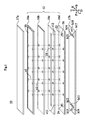
- FIG. 1 is an exploded perspective view of the resin multilayer substrate 10.
- FIG. 2 is a cross-sectional view of the resin multilayer substrate 10.
- FIG. 3 is a front view of the electronic device 1.
- FIG. 1 is an exploded perspective view of the resin multilayer substrate 10.
- FIG. 2 is a cross-sectional view of the resin multilayer substrate 10.
- FIG. 3 is a front view of the electronic device 1.
- the direction is defined as follows.
- the stacking direction of the laminated body 12 of the resin multilayer substrate 10 is defined as the vertical direction.
- the direction in which the signal conductor layer 18 of the resin multilayer substrate 10 extends is defined as the front-rear direction.
- the line width direction of the signal conductor layer 18 of the resin multilayer substrate 10 is defined as the left-right direction.
- the vertical direction, the front-back direction, and the left-right direction are orthogonal to each other.
- the definition of direction in this specification is an example. Therefore, it is not necessary that the direction of the resin multilayer substrate 10 in actual use and the direction in the present specification match.
- the resin multilayer substrate 10 is used for connecting two circuits in an electronic device such as a mobile phone, for example.
- the resin multilayer substrate 10 includes a laminate 12, a signal conductor layer 18, a first ground conductor layer 20, a second ground conductor layer 22, external electrodes 24, 26, and a plurality of first interlayer connection conductors v1.
- a plurality of second interlayer connecting conductors v2 and interlayer connecting conductors v11 and v12 are provided.
- typical interlayer connecting conductors, conductor non-forming portions, and voids among the plurality of first interlayer connecting conductors v1 and the plurality of second interlayer connecting conductors v2 are designated by reference numerals.
- the laminated body 12 has a plate shape. As shown in FIG. 1, the laminated body 12 has a rectangular shape having a long side extending in the front-rear direction when viewed in the vertical direction. Therefore, the length of the laminated body 12 in the front-rear direction is longer than the length of the laminated body 12 in the left-right direction. The length of the laminated body 12 in the front-rear direction is longer than the length of the laminated body 12 in the vertical direction.
- the laminate 12 has flexibility.
- the laminated body 12 has a structure in which resin sheets 16a to 16d and resist layers 17a and 17b are laminated in the vertical direction (lamination direction).
- the resist layer 17a, the resin sheets 16a to 16d, and the resist layer 17b are laminated so as to be arranged in this order from top to bottom.
- the resin sheets 16a to 16d are flexible dielectric sheets. The materials of the resin sheets 16a to 16d will be described later.
- the resin sheets 16a to 16d have the same rectangular shape as the laminated body 12 when viewed in the vertical direction. The details of the resist layers 17a and 17b will be described later.
- the signal conductor layer 18 is provided on the laminated body 12. More specifically, the signal conductor layer 18 is provided on the upper surface of the resin sheet 16c. As a result, the signal conductor layer 18 is provided in the laminated body 12.
- the signal conductor layer 18 has a linear shape extending in the front-rear direction.
- the signal conductor layer 18 is arranged at the center of the upper surface of the resin sheet 16c in the left-right direction.
- the front end of the signal conductor layer 18 is located at the front end of the resin sheet 16c.
- the rear end of the signal conductor layer 18 is located at the rear end of the resin sheet 16c.
- a high frequency signal is transmitted to the signal conductor layer 18.
- the first ground conductor layer 20 is provided on the laminated body 12.
- the first ground conductor layer 20 is arranged on the signal conductor layer 18 so as to overlap the signal conductor layer 18 when viewed in the vertical direction.
- the first ground conductor layer 20 is provided on the upper surface of the resin sheet 16a.
- the first ground conductor layer 20 has a rectangular shape having a long side extending in the front-rear direction when viewed in the vertical direction.
- the first ground conductor layer 20 has a shape that substantially matches the laminated body 12 when viewed in the vertical direction. However, the first ground conductor layer 20 is slightly smaller than the laminated body 12 when viewed in the vertical direction.
- a ground potential is connected to the first ground conductor layer 20.
- the second ground conductor layer 22 is provided on the laminated body 12.
- the second ground conductor layer 22 is arranged below the signal conductor layer 18 so as to overlap the signal conductor layer 18 when viewed in the vertical direction. More specifically, the second ground conductor layer 22 is provided on the lower surface of the resin sheet 16d.
- the second ground conductor layer 22 has a rectangular shape having a long side extending in the front-rear direction when viewed in the vertical direction.
- the second ground conductor layer 22 has a shape that substantially matches the laminated body 12 when viewed in the vertical direction. However, the second ground conductor layer 22 is slightly smaller than the laminated body 12 when viewed in the vertical direction.
- a ground potential is connected to the second ground conductor layer 22.
- the signal conductor layer 18, the first ground conductor layer 20, and the second ground conductor layer 22 have a stripline structure as shown in FIG.
- the external electrode 24 is provided at the left end of the lower surface of the resin sheet 16d.
- the external electrode 24 has a rectangular shape when viewed in the vertical direction.
- a second ground conductor layer 22 is not provided around the external electrode 24 so that the external electrode 24 is insulated from the second ground conductor layer 22.
- the external electrode 24 overlaps the front end portion of the signal conductor layer 18 when viewed in the vertical direction.
- the high frequency signal is input / output to the signal conductor layer 18 via the external electrode 24.
- the external electrode 26 has a structure symmetrical to that of the external electrode 24. Therefore, the description of the external electrode 26 will be omitted.
- the resist layers 17a and 17b are flexible protective layers.
- the resist layers 17a and 17b have the same rectangular shape as the laminated body 12 when viewed in the vertical direction.
- the resist layer 17a covers the entire upper surface of the resin sheet 16a. As a result, the resist layer 17a protects the first ground conductor layer 20.
- the resist layer 17b covers substantially the entire lower surface of the resin sheet 16d. As a result, the resist layer 17b protects the second ground conductor layer 22. However, the resist layer 17b is provided with openings h11 to h18. The opening h11 overlaps with the external electrode 24 when viewed in the vertical direction. As a result, the external electrode 24 is exposed to the outside from the resin multilayer substrate 10 through the opening h11. The opening h12 is provided to the right of the opening h11. The opening h13 is provided in front of the opening h11. The opening h14 is provided to the left of the opening h11. As a result, the second ground conductor layer 22 is exposed to the outside from the resin multilayer substrate 10 through the openings h12 to h14. The openings h15 to h18 each have a structure symmetrical with respect to the openings h11 to h14. Therefore, the description of the openings h15 to h18 will be omitted.
- the signal conductor layer 18, the first ground conductor layer 20, the second ground conductor layer 22, and the external electrodes 24, 26 as described above are, for example, etched on the copper foil provided on the upper surface or the lower surface of the resin sheets 16a to 16d. It is formed by being applied.
- the plurality of first interlayer connecting conductors v1 are provided in the laminated body 12 so as to be located on the left side of the signal conductor layer 18.
- the plurality of first interlayer connecting conductors v1 are arranged so as to be arranged in a line at equal intervals in the front-rear direction.
- the plurality of first interlayer connecting conductors v1 penetrate the resin sheets 16a to 16d in the vertical direction.
- the upper ends of the plurality of first interlayer conductors v1 are connected to the first ground conductor layer 20 as shown in FIG.
- the lower ends of the plurality of first interlayer conductors v1 are connected to the second ground conductor layer 22.
- the plurality of first interlayer connecting conductors v1 electrically connect the first ground conductor layer 20 and the second ground conductor layer 22.
- the plurality of second interlayer connecting conductors v2 are provided in the laminated body 12 so as to be located on the right side of the signal conductor layer 18.
- the plurality of second interlayer connecting conductors v2 are arranged so as to be arranged in a line at equal intervals in the front-rear direction.
- the plurality of second interlayer connecting conductors v2 penetrate the resin sheets 16a to 16d in the vertical direction.
- the upper ends of the plurality of second interlayer connecting conductors v2 are connected to the first ground conductor layer 20 as shown in FIG.
- the lower ends of the plurality of second interlayer connecting conductors v2 are connected to the second ground conductor layer 22.
- the plurality of second interlayer connecting conductors v2 electrically connect the first ground conductor layer 20 and the second ground conductor layer 22.
- the interlayer connection conductor v11 is provided at the front end of the resin sheets 16c and 16d.
- the interlayer connection conductor v11 penetrates the resin sheets 16c and 16d in the vertical direction.
- the upper end of the interlayer connection conductor v11 is connected to the front end portion of the signal conductor layer 18.
- the lower end of the interlayer connection conductor v11 is connected to the external electrode 24.
- the interlayer connection conductor v11 electrically connects the signal conductor layer 18 and the external electrode 24.
- the interlayer connecting conductor v12 has a structure symmetrical to that of the interlayer connecting conductor v11. Therefore, the description of the interlayer connection conductor v12 will be omitted.
- the plurality of first interlayer connecting conductors v1, the plurality of second interlayer connecting conductors v2, and the interlayer connecting conductors v11 and v12 as described above are via hole conductors.
- the formation of the via hole conductor is as follows. Through holes are formed in the resin sheets 16a to 16d by a laser beam. The through holes are filled with a conductive paste that is a mixture of metal and resin. A via hole conductor is formed by firing the conductive paste during thermocompression bonding of the resin sheets 16a to 16d.
- a plurality of first interlayer connecting conductors v1, a plurality of second interlayer connecting conductors v2, and interlayer connecting conductors v11 and v12 can be connected at the time of batch heating pressing of the resin sheets 16a to 16d. Therefore, a plurality of first interlayer connection conductors v1, a plurality of second interlayer connection conductors v2, and interlayer connection conductors v11 and v12 can be easily formed, and a plurality of first interlayer connection conductors v1 and a plurality of second interlayer connection conductors v2 can be easily formed. In addition, the degree of freedom in arranging the interlayer connection conductors v11 and v12 is increased.
- the electronic device 1 includes a resin multilayer board 10 and a circuit board 100.
- the resin multilayer substrate 10 further includes connectors 30a and 30b.
- the connector 30a is mounted on the front end portion of the lower surface of the resist layer 17b.
- the connector 30a includes a central conductor and an outer conductor.
- the center conductor is electrically connected to the external electrode 24 by soldering.
- the outer conductor is electrically connected to the second ground conductor layer 22 by soldering.
- the connector 30b is mounted on the rear end of the lower surface of the resist layer 17b.
- the connector 30b includes a central conductor and an outer conductor.
- the center conductor is electrically connected to the external electrode 26 by soldering.
- the outer conductor is electrically connected to the second ground conductor layer 22 by soldering.
- the circuit board 100 includes a board body 102 and connectors 104a and 104b.
- the substrate body 102 has a plate shape.
- the connector 104a is mounted on the upper surface of the front portion of the board body 102.
- the connector 104a includes a central conductor and an outer conductor.
- the central conductor of the connector 104a is connected to the central conductor of the connector 30a.
- the outer conductor of the connector 104a is connected to the outer conductor of the connector 30a.
- the connector 104b is mounted on the upper surface of the rear portion of the board body 102.
- Connector 104b includes a center conductor and an outer conductor.
- the central conductor of the connector 104b is connected to the central conductor of the connector 30b.
- the outer conductor of the connector 104b is connected to the outer conductor of the connector 30b.
- the resin multilayer substrate 10 is bent and used. Specifically, the upper surface of the laminated body 12 is mountain-folded, and the upper surface of the laminated body 12 is valley-folded. As described above, the resin multilayer substrate 10 has a bent portion 12a in which the stacking direction of the resin sheets 16a to 16d changes.
- the resin sheet before laminating is referred to as the resin sheet 16 to distinguish it from the resin sheets 16a to 16d after laminating.
- the material of the resin sheet 16 preferably has a low relative permittivity and a low dielectric loss tangent from the viewpoint of high frequency characteristics.
- Examples of the material having such a low relative permittivity and a low dielectric loss tangent include PFA (perfluoroalkoxy alkane), COP (cyclic olefin polymer), and SPS (syndiotactic polystyrene).
- PFA perfluoroalkoxy alkane
- COP cyclic olefin polymer
- SPS ndiotactic polystyrene
- PFA for example, Fluon + EA2000 manufactured by AGC Inc.
- COP for example, ZEONOR manufactured by Nippon Zeon Corporation can be used.
- SPS for example, Oidys manufactured by Kurabo Industries Ltd. can be used.
- the resin sheet 16 contains a resin material having a small relative permittivity and a small dielectric loss tangent such as PFA, COP, and S
- the resin multilayer substrate 10 When the coefficient of thermal expansion of the resin material of the resin sheet 16 becomes large, the resin multilayer substrate 10 may be distorted or warped during the production of the resin multilayer substrate 10, as will be described below.
- the resin multilayer substrate 10 includes a conductor layer such as the signal conductor layer 18, the first ground conductor layer 20, and the second ground conductor layer 22.
- the material of the conductor layer is, for example, copper.
- the coefficient of thermal expansion of copper is about 16.
- the coefficient of thermal expansion of PFA is larger than 200.
- the coefficient of thermal expansion of COP is 60 or more.
- the coefficient of thermal expansion of SPS is greater than 60.
- the coefficient of thermal expansion of a resin material having a small relative permittivity and a small dielectric loss tangent such as PFA, COP, and SPS may be larger than the coefficient of thermal expansion of copper. Therefore, in the thermocompression bonding step of the resin sheet 16, the amount of elongation per unit length of the resin sheet 16 and the amount of elongation per unit length of the signal conductor layer 18, the first ground conductor layer 20, and the second ground conductor layer 22 Makes a difference. As a result, the resin multilayer substrate 10 may be distorted or warped.
- the inventor of the present application designed the resin material of the resin sheet 16 as follows.
- the resin sheet 16 contains one or more resin materials and a liquid crystal polymer having a weight less than the total weight of one or more resin materials.
- the one or more kinds of resin materials are the portions of the resin materials contained in the resin sheet 16 excluding the liquid crystal polymer.
- One or more kinds of resin materials have a coefficient of thermal expansion larger than the coefficient of thermal expansion of LCP.
- the resin sheet 16 has a coefficient of thermal expansion in the surface direction that is smaller than the coefficient of thermal expansion in the surface direction of the first comparative resin sheet.
- the first comparative resin sheet is a resin sheet containing one or more kinds of resin materials and not containing LCP.
- the first comparative resin sheet has the same structure as the resin sheet 16.
- the coefficient of thermal expansion of the resin sheet 16 in the plane direction is preferably, for example, 5 ppm / ° C. or higher and 20 ppm / ° C. or lower.
- the coefficient of thermal expansion of the resin sheet 16 in the plane direction is more preferably 10 ppm / ° C. or higher and 20 ppm / ° C. or lower.
- the coefficient of thermal expansion in the plane direction is represented by the following formula (A).
- ⁇ L ⁇ L ⁇ T ...
- A Coefficient of thermal expansion in the direction in which the main surface of the resin sheet 16 spreads (plane direction): ⁇ Length of the resin sheet 16 in the direction in which the main surface of the resin sheet 16 spreads (plane direction): L Amount of elongation of the resin sheet 16 in the direction in which the main surface of the resin sheet 16 spreads (plane direction): ⁇ L Temperature rise: ⁇ T
- the inventor of the present application measured the coefficient of thermal expansion by the following method. The inventor of the present application prepared a sample cut out to a width of 5 mm and a length of 16 mm.
- the inventor of the present application raised the temperature of the sample from room temperature to 170 ° C. in a tension mode with a load of 0.1 N by a thermomechanical analyzer (trade name: TMA Q400) manufactured by TA instruments. Then, the inventor of the present application measured the coefficient of thermal expansion by obtaining the average value of the coefficient of thermal expansion in the range of 50 ° C. to 80 ° C. in the process of cooling the sample to room temperature.
- the relative permittivity of one or more kinds of resin materials is smaller than the relative permittivity of LCP.
- the relative permittivity of one or more kinds of dielectric loss tangents is smaller than the relative permittivity of LCP.
- One or more kinds of resin materials are, for example, fluororesins.
- the fluororesin is, for example, PFA.
- the coefficient of thermal expansion of PFA is larger than the coefficient of thermal expansion of LCP.
- the relative permittivity of PFA is smaller than the relative permittivity of LCP.
- the dielectric loss tangent of PFA is smaller than the dielectric loss tangent of LCP.
- the one or more kinds of resin materials may be, for example, COP.
- the coefficient of thermal expansion of COP is larger than the coefficient of thermal expansion of LCP, as shown in Table 1.
- the relative permittivity of COP is smaller than the relative permittivity of LCP.
- the dielectric loss tangent of COP is smaller than the dielectric loss tangent of LCP.
- the one or more kinds of resin materials may be, for example, SPS.
- the coefficient of thermal expansion of SPS is larger than the coefficient of thermal expansion of LCP, as shown in Table 1.
- the relative permittivity of SPS is smaller than the relative permittivity of LCP.
- the dielectric loss tangent of SPS is smaller than the dielectric loss tangent of LCP.
- the resin sheet 16 contains one or more resin materials having a coefficient of thermal expansion larger than the coefficient of thermal expansion of the LCP, and LCP having a weight less than the total weight of the one or more resin materials. .. Therefore, the coefficient of thermal expansion in the surface direction of the resin sheet 16 is smaller than the coefficient of thermal expansion in the surface direction of the first comparative resin sheet containing one or more kinds of resin materials and not containing LCP. Therefore, the coefficient of thermal expansion of the resin sheet 16 in the surface direction approaches the coefficient of thermal expansion of the conductor layer. As a result, it is possible to prevent the resin multilayer substrate 10 from being distorted or warped during the production of the resin multilayer substrate 10. In particular, when the coefficient of thermal expansion of the resin sheet 16 in the surface direction is 20 ppm / ° C. or less, the occurrence of distortion or warpage in the resin multilayer substrate 10 during the production of the resin multilayer substrate 10 is effectively suppressed.
- LCP has flexibility. Therefore, even if the resin sheet 16 contains LCP, it is possible to prevent the resin sheet 16 from becoming brittle. As a result, the resin multilayer substrate 10 having excellent flexibility can be obtained.
- the relative permittivity of one or more resin materials is smaller than the relative permittivity of LCP.
- the relative permittivity of the resin sheet 16 is lower than the relative permittivity of the second comparative resin sheet containing only LCP as the resin material.
- the high frequency characteristics of the resin multilayer substrate 10 are improved.
- the dielectric loss tangent of one or more kinds of resin materials is smaller than the dielectric loss tangent of LCP, the dielectric loss tangent of the resin sheet 16 is lower than the dielectric loss tangent of the second comparative resin sheet containing only LCP as the resin material. As a result, the high frequency characteristics of the resin multilayer substrate 10 are improved.
- the resin sheet 16 may contain an LCP having a weight less than the total weight of one or more kinds of resin materials.
- the resin sheet 16 preferably contains 100 parts by weight or more of one or more resin materials and 10 parts by weight or more and 70 parts by weight or less of LCP.
- the resin sheet 16 contains 100 parts by weight or more of one or more resin materials and 15 parts by weight or more and 50 parts by weight or less of LCP. It is particularly preferable that the resin sheet 16 contains 100 parts by weight or more of one or more resin materials and 20 parts by weight or more and 40 parts by weight or less of LCP.
- the LCP preferably contains fibrous particles.
- the LCP is preferably LCP-NF (nanofiber liquid crystal polymer).
- LCP-NF nanofiber liquid crystal polymer
- LCP-NF includes a fiber portion and a lump portion.
- the fibrous portion may be contained in LCP-NF as an agglomerated portion in which fibrous particles are aggregated, and the agglomerated portion may be contained in LCP as an agglomerated portion in which agglomerated particles are contained. ..
- the LCP-NF does not have to include a lumpy portion.
- the fiber part is a fibrous particle.
- the fibrous particles are LCP particles having an aspect ratio of 10 times or more, which is the ratio of the length in the longitudinal direction to the fiber diameter.
- the longitudinal length and fiber diameter of the fibrous particles can be measured from the image data of the fibrous particles obtained when the fibrous particles are observed with a scanning electron microscope.
- the average diameter of fibrous particles is 1 ⁇ m or less.
- the value of the average diameter of the fiber portion is the average value of the fiber diameters of the plurality of fibrous particles constituting the fiber portion.
- the LCP-NF according to the present embodiment contains fine fibrous particles.
- the lumpy part is LCP-NF which is not substantially fibrous.
- the lumpy portion may have a flat outer shape.
- LCP-NF the content of the lump portion is 20% or less. That is, in LCP-NF, the content of the lumpy portion is relatively low, or LCP-NF does not contain the lumpy portion.
- the content of the lumpy portion is evaluated by the number of lumpy portions relative to the number of agglomerated portions contained in LCP-NF. When the LCP-NF is placed on a flat surface, the agglomerated portion having a maximum height of more than 10 ⁇ m is the agglomerated portion, and the agglomerated portion having a maximum height of 10 ⁇ m or less is the fiber portion.
- the LCP is LCP-NF
- the coefficient of thermal expansion of the resin sheet 16 in the surface direction becomes smaller.
- the fibrous particles have an aspect ratio of 10 times or more, which is the ratio of the length in the longitudinal direction to the fiber diameter. Further, the average diameter of the fibrous particles is 1 ⁇ m or less.
- Such LCP-NF has a property of having a large surface area. Therefore, LCP-NF easily adheres to other members (that is, one or more kinds of resin materials). Further, the coefficient of thermal expansion in the longitudinal direction of the main chain structure of LCP-NF is negative. As a result, the LCP-NF effectively prevents the extension of one or more kinds of resin materials when the temperature of the resin sheet 16 rises.
- the coefficient of thermal expansion of the resin sheet 16 in the surface direction becomes smaller. Further, since the resin sheet 16 contains a small amount of LCP-NP, the coefficient of thermal expansion of the resin sheet 16 in the surface direction becomes sufficiently small.
- the coefficient of thermal expansion of the resin sheet 16 in the surface direction becomes smaller because the LCP is LCP-NF. More specifically, when the resin sheet 16 is formed, a solution in which one or more kinds of resin materials are melted in a solvent is prepared. Further, LCP-NF is mixed with the solution. This solution is spread on a metal plate by spin coating or the like. Then, in the drying step, the solvent is volatilized. As the solvent volatilizes, the thickness of the solution becomes thinner. LCP-NF is a fibrous particle. Therefore, the fibrous particles collapse in the solution. As a result, the longitudinal direction of the main chain structure of the LCP-NF becomes a direction along the surface direction of the resin sheet 16 as shown in FIG.
- the coefficient of thermal expansion in the longitudinal direction of the main chain structure of LCP-NF is negative.
- the LCP-NF effectively prevents one or more kinds of resin materials from extending in the plane direction.
- the coefficient of thermal expansion in the surface direction of the resin sheet 16 becomes smaller.
- the resin sheet 16 contains a small amount of LCP-NP, the coefficient of thermal expansion of the resin sheet 16 in the surface direction becomes sufficiently small.
- LCP-NF is made of a thermotropic liquid crystal polymer.
- the LCP-NF is heated to 400 ° C. in an inert atmosphere, cooled to room temperature at a temperature lowering rate of 40 ° C./min or higher, and heated again at a heating rate of 40 ° C./min using a differential scanning calorimeter.
- the endothermic peak temperature measured above exceeds 330 ° C.
- LCP-NF has high heat resistance and can be used as an electronic material.
- the endothermic peak temperature measured as described above may be simply referred to as "melting point".
- the value of D50 measured by particle size measurement using a particle size distribution measuring device by a laser diffraction / scattering method is preferably 13 ⁇ m or less.
- the method for producing LCP-NF includes a coarse pulverization step, a fine pulverization step, a coarse grain removal step, and a fibrosis step in this order.
- an LCP molded product is prepared as a raw material.
- the LCP molded product include uniaxially oriented pellets, biaxially oriented films, and powdered LCPs.
- pellet-shaped or powder-shaped LCP is preferable, and pellet-shaped LCP is more preferable, from the viewpoint of manufacturing cost and the like.
- the molded product of LCP does not include fibrous LCP directly molded by an electrolytic spinning method, a melt blow method, or the like.
- the molded product of LCP may contain LCP in the form of pellets or LCP in the form of fibers by crushing the LCP in the form of powder.
- the melting point of the LCP molded product is preferably larger than 330 ° C, more preferably 350 ° C or higher. As a result, LCP-NF with high heat resistance suitable as a material for electronic parts can be obtained.
- the coarsely pulverized LCP is obtained by coarsely pulverizing the molded product of LCP.
- a coarsely pulverized LCP is obtained by coarsely pulverizing a molded product of LCP with a cutter mill device.
- the particle size of the coarsely pulverized LCP is not particularly limited as long as it can be used as a raw material for the fine pulverization step described later.
- the maximum particle size of the coarsely pulverized LCP is, for example, 3 mm or less.
- the method for producing LCP-NF does not necessarily have to include a coarse pulverization step.
- the LCP molded product can be used as a raw material for the pulverization step
- the LCP molded product may be directly used as a raw material for the pulverization step.
- LCP coarse powder LCP is pulverized in a state of being dispersed in liquid nitrogen to obtain granular fine pulverized LCP.
- a medium is used to pulverize the coarsely pulverized LCP dispersed in liquid nitrogen.
- the media is, for example, beads.
- the pulverization method in which LCP is dispersed in liquid nitrogen is different from the conventional freeze pulverization method.
- the conventional freeze crushing method is a method of crushing the raw material to be crushed while pouring liquid nitrogen onto the raw material to be crushed and the main body of the crushing device, but the liquid nitrogen is vaporized when the raw material to be crushed is crushed. That is, in the conventional freeze pulverization method, the raw material to be crushed is not dispersed in liquid nitrogen at the time when the raw material to be pulverized is pulverized.
- the heat of the raw material to be crushed, the heat generated from the crushing device, and the heat generated by crushing the raw material to be crushed vaporize liquid nitrogen in an extremely short time. Therefore, in the conventional freeze pulverization method, the raw material during pulverization located inside the pulverizer has a temperature much higher than the boiling point of liquid nitrogen, which is -196 ° C. That is, in the conventional freeze pulverization method, pulverization is carried out under the condition that the temperature inside the pulverizer is usually about 0 ° C. to 100 ° C. In the conventional freeze pulverization method, even when liquid nitrogen is supplied as much as possible, the temperature inside the pulverizer is about ⁇ 150 ° C. at the lowest case.
- the raw material to be crushed is crushed in a state of being dispersed in liquid nitrogen, the raw material in a further cooled state can be crushed as compared with the conventional freeze crushing method.
- the raw material to be pulverized can be pulverized at a temperature lower than -196 ° C., which is the boiling point of liquid nitrogen.
- the brittle fracture of the raw material to be pulverized is repeated, so that the pulverization of the raw material proceeds.
- the LCP that has become granular due to brittle fracture in liquid nitrogen is continuously impacted with a medium or the like in a brittle state.
- a plurality of fine cracks are formed in the LCP obtained in the fine pulverization step from the outer surface to the inner side.
- the granular finely pulverized LCP obtained by the pulverization step preferably has a D50 of 50 ⁇ m or less as measured by a particle size distribution measuring device by a laser diffraction / scattering method. As a result, it is possible to prevent the granular finely pulverized LCP from being clogged with the nozzle in the fibrosis step shown below.
- the coarse grain removing step coarse grains are removed from the granular finely pulverized LCP obtained in the above fine pulverization step. For example, by sieving the granular pulverized LCP with a mesh, the granular pulverized LCP under the sieve is obtained, and by removing the granular LCP on the sieve, the coarse particles contained in the granular pulverized LCP are obtained. Can be removed.
- the type of mesh may be appropriately selected, and examples of the mesh include those having a mesh opening of 53 ⁇ m.
- the method for producing LCP-NF does not necessarily have to include a coarse grain removing step.
- the finely pulverized LCP is dispersed in a dispersion medium.
- the finely pulverized LCP to be dispersed does not have to have coarse particles removed, but it is preferable that coarse particles have been removed.
- the dispersion medium include water, ethanol, methanol, isopropyl alcohol, toluene, benzene, xylene, phenol, acetone, methyl ethyl ketone, diethyl ether, dimethyl ether, hexane, or a mixture thereof.
- the finely pulverized LCP dispersed in the dispersion medium that is, the slurry-like finely pulverized LCP is passed through the nozzle in a state of being pressurized at a high pressure.
- the shearing force or collision energy due to the high-speed flow at the nozzle acts on the LCP, and by crushing the granular finely pulverized LCP, the fibrosis of the LCP progresses and LCP-NF is produced. Obtainable.
- the nozzle diameter of the nozzle is preferably made as small as possible within a range in which clogging of the finely pulverized LCP does not occur in the nozzle. Since the granular finely pulverized LCP has a relatively small particle size, the nozzle diameter in the wet high pressure crushing apparatus used in the fibrosis step can be reduced.
- the nozzle diameter is, for example, 0.2 mm or less.
- a plurality of fine cracks are formed in the granular finely pulverized LCP-NF. Therefore, by pressurizing with a wet high-pressure disperser, the dispersion medium penetrates into the inside of the finely pulverized LCP through fine cracks. Then, when the slurry-like pulverized LCP passes through the nozzle and is located under normal pressure, the dispersion medium that has penetrated into the pulverized LCP expands in a short time. As the dispersion medium that has penetrated into the pulverized LCP expands, destruction proceeds from the inside of the pulverized LCP.
- fibrosis proceeds to the inside of the finely pulverized LCP, and the molecules of the LCP are separated into domain units in which they are arranged in one direction.
- LCP- obtained by crushing the granular LCP obtained by the conventional freeze pulverization method by defibrating the granular finely pulverized LCP obtained in the fine pulverization step It is possible to obtain LCP-NF which has a lower content of the lumpy portion than NF and is in the form of fine fibers.
- the method for producing the resin sheet 16 containing LCP-NF is a solution film formation in which a resin is dissolved in a solvent, a dispersion coating in which the resin is dispersed in a solvent, and a melt film formation in which the resin is melted and molded at a melting temperature or higher. Any can be produced.
- a solution in which one or more resin materials are dissolved in a solvent is prepared.
- One or more kinds of resin materials are, for example, PFA, COP, SPS and the like.
- the solvent is a liquid capable of dissolving one or more resin materials such as PFA, COP, and SPS.
- Such solvents include, for example, toluene, xylene, N-methylpyrrolidone, dimethylformamide, dimethylacetamide, methylethylketone, fatty alcohols, water and the like.
- LCP-NF is mixed with the above solution.
- the solvent cannot dissolve the LCP-NF.
- the solvent does not disrupt the structure of the LCP-NF. Therefore, LCP-NF is dispersed in a solution in which one or more resin materials are dissolved in a solvent while maintaining the state of fibrous particles.
- the resin sheet 16 may be produced by a melt film forming method. First, a mixed material in which one or more kinds of resin materials and LCP-NF are mixed is prepared. One or more kinds of resin materials are, for example, PFA, COP, SPS and the like.
- the mixed material by heating the mixed material, one or more resin materials of the mixed material are melted. However, in the melted mixed material, one or more kinds of resin materials are melted, and LCP-NF is not melted. Further, the structure of LCP-NF does not collapse due to heating of the mixed material. Therefore, the highest melting point among the melting points of one or more kinds of resin materials is preferably 30 ° C. or more lower than the melting point of LCP-NF (liquid crystal polymer). Further, one or more kinds of resin materials are heat-resistant thermoplastic resins whose composition does not collapse by heating. After that, the molten mixed material is extruded into a sheet. As a result, the resin sheet 16 is completed.
- the resin sheet according to the present invention is not limited to the resin sheets 16, 16a to 16d according to the embodiment, and can be changed within the scope of the gist thereof.
- the resin sheets 16, 16a to 16d may contain one or more resin materials having a coefficient of thermal expansion larger than the coefficient of thermal expansion of LCP. Therefore, the resin sheets 16, 16a to 16d may contain one type of resin material having a coefficient of thermal expansion larger than the coefficient of thermal expansion of LCP, or two types having a coefficient of thermal expansion larger than the coefficient of thermal expansion of LCP. The above resin materials may be included.
- the content of one or more kinds of resin materials is larger than 50% of the total of the resin sheets 16, 16a to 16d.
- the relative permittivity of one or more kinds of resin materials is preferably smaller than the relative permittivity of LCP. This does not prevent the relative permittivity of one or more kinds of resin materials from being equal to or higher than the relative permittivity of LCP.
- the dielectric loss tangent of one or more kinds of resin materials is preferably smaller than the dielectric loss tangent of LCP. This does not prevent the dielectric loss tangent of one or more resin materials from being greater than the dielectric loss tangent of the LCP.
- the LCP does not have to be LCP-NF. Even when the LCP is not LCP-NF, the coefficient of thermal expansion in the plane direction of the resin sheets 16, 16a to 16d can be reduced.
- the solvent can melt one or more kinds of resin materials and LCP during the production of the resin sheet 16. As a result, one or more kinds of resin materials and LCP are uniformly mixed in the resin sheets 16, 16a to 16d. As a result, various characteristics of the resin sheets 16, 16a to 16d become uniform.
- the LCP is not LCP-NF, one or more resin materials of the mixed material and the LCP are melted by heating the mixed material at the time of manufacturing the resin sheet 16. As a result, one or more kinds of resin materials and LCP are uniformly mixed in the resin sheets 16, 16a to 16d. As a result, various characteristics of the resin sheets 16, 16a to 16d become uniform.
- the one or more kinds of resin materials may be, for example, a norbornene-based polymer containing at least one of the repeating units represented by the following general formula (1).
- X represents O, -CH 2- or -CH 2- CH 2-
- the substituents R 1 , R 2 , R 3 and R 4 are hydrogen, linear or branched, respectively.
- An organic group or a group containing a group selected from a derivative in which a part of these organic groups is substituted with a halogen or a nitrile group is shown.
- the organic group contains, for example, an alkyl group, an alkenyl group, an alkynyl group, an aryl group, an aralkyl group, an alkoxysilyl group, an organic group containing an epoxy group, an organic group containing an ether group, and a (meth) acrylic group.
- m is an integer from 10 to 10000
- n 1 is an integer from 0 to 5.
- R 1 of the addition-type polynorbornene having a structure represented by (1), R 2, R 3 and R 4 are, depending on the purpose, by adjusting the proportion of the types and the repeating unit It can have predetermined characteristics.
- X is -CH 2-
- m is 1000 or more, n 1 is 0 or 1, and at least one of R 1 , R 2 , R 3 and R 4 contains an ester group, an ether group or a hydroxyl group. Is preferable. More preferably, m is 5000 or more, n 1 is 0, and at least one of R 1 , R 2 , R 3 and R 4 contains an ester group or a hydroxyl group.
- Examples of the alkyl group include linear or branched saturated hydrocarbons having 1 to 10 carbon atoms, cyclic saturated hydrocarbons, and the like.
- Examples of the alkenyl group include vinyl, allyl, butynyl, cyclohexenyl group and the like.
- Examples of the alkynyl group include ethynyl, 1-propynyl, 2-propynyl, 1-butynyl, 2-butynyl, hexynyl, octynyl, and heptynyl groups.
- Examples of the aryl group include phenyl, trill, naphthyl, anthracenyl group and the like.
- Examples of the aralkyl group include a benzyl group and a phenethyl group.
- the epoxy group include a glycidyl ether group and the like, and examples of the alkoxysilyl group include a trimethoxysilyl group, a triethoxysilyl group and a triethoxysilylethyl group.
- examples of the (meth) acrylic group include a methacryloxymethyl group, and examples of the ester group include methyl ester, ethyl ester, n-propyl ester, n-butyl ester, t-butyl ester group and the like.
- the one or more resin materials may be PEEK (polyetheretherketone), PPO (polyphenylene oxide), or other resins.
- PEEK polyetheretherketone
- PPO polyphenylene oxide
- EXPEEK manufactured by Kurabo Industries Ltd. can be used.
- the resin multilayer substrate 10 does not have to have the bent portion 12a.
- a high-frequency transmission signal line was given as an example of the resin multilayer substrate 10.
- the resin multilayer board 10 may be a high frequency circuit board such as an antenna.
- the first interlayer connection conductor v1, the second interlayer connection conductor v2, and the interlayer connection conductors v11 and v12 may be through-hole conductors.
- the through-hole conductor is formed by plating the through holes formed in the resin sheets 16a to 16d with Cu. When the plating method is used, it is common to plate through holes formed across a plurality of insulating layers after lamination, but since the metal bonds are made of the same metal, the connection is highly reliable and the conductor resistance. Is also easy to make small.
Abstract
樹脂シートは、液晶ポリマーの熱膨張係数より大きい熱膨張係数を有する1種以上の樹脂材料と、1種以上の樹脂材料の重量の合計より少ない重量の液晶ポリマーとを、含んでいる。樹脂シートは、1種以上の樹脂材料を含み、かつ、液晶ポリマーを含まない比較樹脂シートが有する面方向の熱膨張係数より小さい面方向の熱膨張係数を有している。
Description
本発明は、樹脂材料により作製された樹脂シート及び樹脂多層基板に関する。
従来、高速通信用回路基板の誘電体として、低誘電率及び低誘電正接を有する誘電体材料を用いた銅貼り積層板及び多層プリント基板が検討されている。低誘電率及び低誘電正接を有する誘電体材料として、環状オレフィンポリマーやフッ素樹脂材料等の熱可塑性樹脂の開発が盛んである。一方で、低誘電率及び低誘電正接を有する熱可塑性樹脂は、高い熱膨張係数を有している。そのため、熱可塑性樹脂の熱膨張係数と導体である銅箔の熱膨張係数との差により、熱負荷による変形差から、反り、精度悪化、ハンドリング性の悪化が生じる。
従来の樹脂シートに関する発明としては、例えば、特許文献1に記載の多層プリント回路基板が知られている。この多層プリント回路基板では、フッ素系基材層が積層された構造を有している。フッ素系基材層は、ガラスクロスに未焼結のPTFE(ポリテトラフロオロエチレン)を含浸させたプリプレグである。ガラスクロスの熱膨張係数は、PTFEの熱膨張係数より低い。これにより、フッ素系基材層の熱膨張係数が低下する。その結果、特許文献1に記載の多層プリント回路基板では、多層プリント回路基板内の導電体層の熱膨張係数とフッ素系基材層の熱膨張係数との差に起因する多層プリント回路基板の歪や反りが抑制される。
ところで、ガラスクロスがフッ素系基材層に含まれると、多層プリント回路基板の脆くなる。そのため、多層プリント回路基板を曲げて用いることが難しくなる。
本発明の目的は、樹脂シートの熱膨張係数を低下させつつ、樹脂シートが脆くなることを抑制できる樹脂シート及び樹脂多層基板を提供することである。
ここで、ガラスクロス等の無機物は、熱膨張係数を低下させる機能を有する。しかしながら、ガラスクロス等の無機物は、高誘電率及び高誘電正接を有する。そのため、ガラスクロスなどの無機物がフッ素系基材層に添加されると、フッ素系基材層の誘電特性が悪化する。本願発明者は、このような観点から、ガラスクロス等の無機物に代わる材料について検討したところ、本願発明に思い至った。
本発明の樹脂多層基板は、
1種以上の樹脂材料と、前記1種以上の樹脂材料の重量の合計より少ない重量の液晶ポリマーとを、含んでおり、
前記1種以上の樹脂材料を含み、かつ、前記液晶ポリマーを含まない比較樹脂シートが有する面方向の熱膨張係数より小さい面方向の熱膨張係数を有している。
1種以上の樹脂材料と、前記1種以上の樹脂材料の重量の合計より少ない重量の液晶ポリマーとを、含んでおり、
前記1種以上の樹脂材料を含み、かつ、前記液晶ポリマーを含まない比較樹脂シートが有する面方向の熱膨張係数より小さい面方向の熱膨張係数を有している。
本発明によれば、樹脂シートの熱膨張係数を低下させつつ、樹脂シートが脆くなることを抑制できる。
[樹脂多層基板の構造]
以下に、本発明の実施形態に係る樹脂多層基板10の構造について図面を参照しながら説明する。図1は、樹脂多層基板10の分解斜視図である。図2は、樹脂多層基板10の断面図である。図3、電子機器1の正面図である。
以下に、本発明の実施形態に係る樹脂多層基板10の構造について図面を参照しながら説明する。図1は、樹脂多層基板10の分解斜視図である。図2は、樹脂多層基板10の断面図である。図3、電子機器1の正面図である。
まず、本明細書において、方向を以下のように定義する。樹脂多層基板10の積層体12の積層方向を上下方向と定義する。樹脂多層基板10の信号導体層18が延びる方向を前後方向と定義する。樹脂多層基板10の信号導体層18の線幅方向を左右方向と定義する。上下方向、前後方向及び左右方向は、互いに直交している。なお、本明細書における方向の定義は、一例である。従って、樹脂多層基板10の実使用時における方向と本明細書における方向とが一致している必要はない。
樹脂多層基板10は、例えば、携帯電話等の電子機器内において、2つの回路を接続するために用いられる。樹脂多層基板10は、図1に示すように、積層体12、信号導体層18、第1グランド導体層20、第2グランド導体層22、外部電極24,26、複数の第1層間接続導体v1、複数の第2層間接続導体v2及び層間接続導体v11,v12を備えている。
なお、図1では、複数の第1層間接続導体v1及び複数の第2層間接続導体v2の内の代表的な層間接続導体、導体非形成部及び空隙に参照符号を付した。
積層体12は、板形状を有している。積層体12は、図1に示すように、上下方向に見て、前後方向に延びる長辺を有する長方形状を有している。従って、積層体12の前後方向の長さは、積層体12の左右方向の長さより長い。積層体12の前後方向の長さは、積層体12の上下方向の長さより長い。積層体12は、可撓性を有する。
積層体12は、図1に示すように、樹脂シート16a~16d及びレジスト層17a,17bが上下方向(積層方向)に積層された構造を有している。レジスト層17a、樹脂シート16a~16d及びレジスト層17bは、上から下へとこの順に並ぶように積層されている。樹脂シート16a~16dは、可撓性を有する誘電体シートである。樹脂シート16a~16dの材料については後述する。樹脂シート16a~16dは、上下方向に見て、積層体12と同じ長方形状を有している。また、レジスト層17a,17bの詳細については後述する。
信号導体層18は、図1に示すように、積層体12に設けられている。より詳細には、信号導体層18は、樹脂シート16cの上面に設けられている。これにより、信号導体層18は、積層体12内に設けられている。信号導体層18は、前後方向に延びる線形状を有している。信号導体層18は、樹脂シート16cの上面の左右方向の中央に配置されている。信号導体層18の前端は、樹脂シート16cの前端部に位置している。信号導体層18の後端は、樹脂シート16cの後端部に位置している。信号導体層18には、高周波信号が伝送される。
第1グランド導体層20は、積層体12に設けられている。第1グランド導体層20は、上下方向に見て信号導体層18と重なるように、信号導体層18の上に配置されている。第1グランド導体層20は、樹脂シート16aの上面に設けられている。第1グランド導体層20は、図1に示すように、上下方向に見て、前後方向に延びる長辺を有する長方形状を有している。第1グランド導体層20は、上下方向に見て、積層体12と略一致する形状を有している。ただし、第1グランド導体層20は、上下方向に見て、積層体12より僅かに小さい。第1グランド導体層20には、グランド電位が接続される。
第2グランド導体層22は、積層体12に設けられている。第2グランド導体層22は、上下方向に見て、信号導体層18と重なるように、信号導体層18の下に配置されている。より詳細には、第2グランド導体層22は、樹脂シート16dの下面に設けられている。第2グランド導体層22は、図1に示すように、上下方向に見て、前後方向に延びる長辺を有する長方形状を有している。第2グランド導体層22は、上下方向に見て、積層体12と略一致する形状を有している。ただし、第2グランド導体層22は、上下方向に見て、積層体12より僅かに小さい。第2グランド導体層22には、グランド電位が接続される。以上のような、信号導体層18、第1グランド導体層20及び第2グランド導体層22は、図2に示すように、ストリップライン構造を有している。
外部電極24は、樹脂シート16dの下面の左端部に設けられている。外部電極24は、上下方向に見て、長方形状を有している。外部電極24が第2グランド導体層22と絶縁されるように、外部電極24の周囲には第2グランド導体層22が設けられていない。外部電極24は、上下方向に見て、信号導体層18の前端部と重なっている。高周波信号は、外部電極24を介して、信号導体層18に入出力する。外部電極26は、外部電極24と前後対称な構造を有する。従って、外部電極26の説明を省略する。
レジスト層17a,17bは、可撓性を有する保護層である。レジスト層17a,17bは、上下方向に見て、積層体12と同じ長方形状を有している。レジスト層17aは、樹脂シート16aの上面の全面を覆っている。これにより、レジスト層17aは、第1グランド導体層20を保護している。
レジスト層17bは、樹脂シート16dの下面の略全面を覆っている。これにより、レジスト層17bは、第2グランド導体層22を保護している。ただし、レジスト層17bには、開口h11~h18が設けられている。開口h11は、上下方向に見て、外部電極24と重なっている。これにより、外部電極24は、開口h11を介して樹脂多層基板10から外部に露出している。開口h12は、開口h11の右に設けられている。開口h13は、開口h11の前に設けられている。開口h14は、開口h11の左に設けられている。これにより、第2グランド導体層22は、開口h12~h14を介して樹脂多層基板10から外部に露出している。なお、開口h15~h18はそれぞれ、開口h11~h14と前後対称な構造を有する。従って、開口h15~h18の説明を省略する。
以上のような信号導体層18、第1グランド導体層20、第2グランド導体層22及び外部電極24,26は、例えば、樹脂シート16a~16dの上面又は下面に設けられた銅箔にエッチングが施されることにより形成されている。
複数の第1層間接続導体v1は、信号導体層18の左に位置するように、積層体12に設けられている。複数の第1層間接続導体v1は、前後方向に等間隔に一列に並ぶように配置されている。複数の第1層間接続導体v1は、樹脂シート16a~16dを上下方向に貫通している。複数の第1層間接続導体v1の上端は、図2に示すように、第1グランド導体層20に接続されている。複数の第1層間接続導体v1の下端は、図2に示すように、第2グランド導体層22に接続されている。これにより、複数の第1層間接続導体v1は、第1グランド導体層20と第2グランド導体層22とを電気的に接続している。
複数の第2層間接続導体v2は、信号導体層18の右に位置するように、積層体12に設けられている。複数の第2層間接続導体v2は、前後方向に等間隔に一列に並ぶように配置されている。複数の第2層間接続導体v2は、樹脂シート16a~16dを上下方向に貫通している。複数の第2層間接続導体v2の上端は、図2に示すように、第1グランド導体層20に接続されている。複数の第2層間接続導体v2の下端は、図2に示すように、第2グランド導体層22に接続されている。これにより、複数の第2層間接続導体v2は、第1グランド導体層20と第2グランド導体層22とを電気的に接続している。
層間接続導体v11は、樹脂シート16c,16dの前端部に設けられている。層間接続導体v11は、樹脂シート16c,16dを上下方向に貫通している。層間接続導体v11の上端は、信号導体層18の前端部に接続されている。層間接続導体v11の下端は、外部電極24に接続されている。これにより、層間接続導体v11は、信号導体層18と外部電極24とを電気的に接続している。なお、層間接続導体v12は、層間接続導体v11と前後対称な構造を有する。従って、層間接続導体v12の説明を省略する。
以上のような複数の第1層間接続導体v1、複数の第2層間接続導体v2及び層間接続導体v11,v12は、ビアホール導体である。ビアホール導体の形成は、以下の通りである。レーザービームにより樹脂シート16a~16dに貫通孔を形成する。金属と樹脂との混合物である導電性ペーストを貫通孔に充填する。樹脂シート16a~16dの熱圧着の際に導電性ペーストが焼成されることにより、ビアホール導体が形成される。導電性ペーストが用いられることにより、樹脂シート16a~16dの一括加熱プレス時に、複数の第1層間接続導体v1、複数の第2層間接続導体v2及び層間接続導体v11,v12を接続できる。そのため、複数の第1層間接続導体v1、複数の第2層間接続導体v2及び層間接続導体v11,v12を容易に形成できると共に、複数の第1層間接続導体v1、複数の第2層間接続導体v2及び層間接続導体v11,v12の配置の自由度が高くなる。
次に、樹脂多層基板10を備える電子機器1について図3を参照しながら説明する。電子機器1は、樹脂多層基板10及び回路基板100を備えている。樹脂多層基板10は、コネクタ30a,30bを更に備えている。コネクタ30aは、レジスト層17bの下面の前端部に実装される。コネクタ30aは、中心導体及び外導体を含んでいる。中心導体は、はんだにより外部電極24に電気的に接続される。外導体は、はんだにより第2グランド導体層22に電気的に接続される。
コネクタ30bは、レジスト層17bの下面の後端部に実装される。コネクタ30bは、中心導体及び外導体を含んでいる。中心導体は、はんだにより外部電極26に電気的に接続される。外導体は、はんだにより第2グランド導体層22に電気的に接続される。
回路基板100は、基板本体102及びコネクタ104a,104bを備えている。基板本体102は、板形状を有している。コネクタ104aは、基板本体102の前部の上面に実装されている。コネクタ104aは、中心導体及び外導体を含んでいる。コネクタ104aの中心導体は、コネクタ30aの中心導体に接続される。コネクタ104aの外導体は、コネクタ30aの外導体に接続される。
コネクタ104bは、基板本体102の後部の上面に実装されている。コネクタ104bは、中心導体及び外導体を含んでいる。コネクタ104bの中心導体は、コネクタ30bの中心導体に接続される。コネクタ104bの外導体は、コネクタ30bの外導体に接続される。
ところで、図3に示すように、コネクタ104aの上下方向における位置は、コネクタ104bの上下方向における位置と異なる。そのため、樹脂多層基板10は、曲げられて使用される。具体的には、積層体12の上面が山折りされている共に、積層体12の上面が谷折りされている。このように、樹脂多層基板10は、樹脂シート16a~16dの積層方向が変化する曲げ部12aを、有している。
[樹脂シートの樹脂材料]
次に、本実施形態に係る樹脂シートの樹脂材料について説明する。なお、積層前の樹脂シートを積層後の樹脂シート16a~16dと区別して、樹脂シート16と呼ぶ。
次に、本実施形態に係る樹脂シートの樹脂材料について説明する。なお、積層前の樹脂シートを積層後の樹脂シート16a~16dと区別して、樹脂シート16と呼ぶ。
樹脂シート16の材料は、高周波特性の観点から低い比誘電率及び低い誘電正接を有していることが好ましい。このような、低い比誘電率及び低い誘電正接を有している材料としては、例えば、PFA(パーフルオロアルコキシアルカン)、COP(環状オレフィンポリマー)、SPS(シンジオタクチックポリスチレン)が挙げられる。PFAには、例えば、AGC株式会社製のFluon+EA2000を用いることができる。COPには、例えば、日本ゼオン株式会社製のZEONORを用いることができる。SPSには、例えば、クラボウ社製のOidysを用いることができる。樹脂シート16がPFA、COP、SPSのような小さな比誘電率及び小さな誘電正接を有する樹脂材料を含んでいると、高周波特性に優れた樹脂多層基板10が得られる。
しかしながら、PFA、COP、SPSのような小さな比誘電率及び小さな誘電正接を有する樹脂材料は、表1に示すように、大きな熱膨張係数を有している。PFA、COP、SPS及びLCP(液晶ポリマー)の物性値を示した表である。

樹脂シート16の樹脂材料の熱膨張係数が大きくなると、以下に説明するように、樹脂多層基板10の製造時に樹脂多層基板10に歪や反りが発生する場合がある。樹脂多層基板10は、信号導体層18、第1グランド導体層20及び第2グランド導体層22のように導体層を備えている。導体層の材料は、例えば、銅である。銅の熱膨張係数は、約16である。一方、表1に示すように、PFAの熱膨張係数は、200より大きい。COPの熱膨張係数は、60以上である。SPSの熱膨張係数は、60より大きい。このように、PFA、COP、SPSのような小さな比誘電率及び小さな誘電正接を有する樹脂材料の熱膨張係数は、銅の熱膨張係数より大きい場合がある。そのため、樹脂シート16の熱圧着工程において、樹脂シート16の単位長さ当たりの伸び量と信号導体層18、第1グランド導体層20及び第2グランド導体層22の単位長さ当たりの伸び量とに差が生じる。その結果、樹脂多層基板10に歪や反りが発生する場合がある。
そこで、本願発明者は、樹脂シート16の樹脂材料を以下の様に設計した。樹脂シート16は、1種以上の樹脂材料、及び、1種以上の樹脂材料の重量の合計より少ない重量の液晶ポリマーを含んでいる。なお、1種以上の樹脂材料は、樹脂シート16に含まれる樹脂材料の内の液晶ポリマーを除く部分である。1種以上の樹脂材料は、LCPの熱膨張係数より大きい熱膨張係数を有している。これにより、樹脂シート16は、第1比較樹脂シートが有する面方向の熱膨張係数より小さい面方向の熱膨張係数を有している。第1比較樹脂シートとは、1種以上の樹脂材料を含み、かつ、LCPを含まない樹脂シートである。第1比較樹脂シートは、樹脂シート16と同じ構造を有している。樹脂シート16の面方向の熱膨張係数は、例えば、5ppm/℃以上20ppm/℃以下であることが好ましい。樹脂シート16の面方向の熱膨張係数は、10ppm/℃以上20ppm/℃以下であることがより好ましい。
面方向の熱膨張係数とは、以下の式(A)で表される。
ΔL=αLΔT・・・(A)
樹脂シート16の主面が広がる方向(面方向)の熱膨張係数:α
樹脂シート16の主面が広がる方向(面方向)における樹脂シート16の長さ:L
樹脂シート16の主面が広がる方向(面方向)における樹脂シート16の伸び量:ΔL
温度上昇:ΔT
なお、本願発明者は、熱膨張係数の測定を以下の手法により行った。本願発明者は、幅5mm、長さ16mmに切り出したサンプルを作製した。そして、本願発明者は、TA instruments社製熱機械的分析装置(商品名:TMA Q400)により、荷重0.1Nの引張りモードで室温から170℃までサンプルを昇温させた。そして、本願発明者は、サンプルを室温まで冷却する過程において、50℃~80℃の範囲内の熱膨張係数の平均値を求めることにより、熱膨張係数を測定した。
更に、1種以上の樹脂材料の比誘電率は、LCPの比誘電率より小さい。また、1種以上の誘電正接の比誘電率は、LCPの比誘電率より小さい。
1種以上の樹脂材料は、例えば、フッ素樹脂である。フッ素樹脂は、例えば、PFAである。PFAの熱膨張係数は、表1に示すように、LCPの熱膨張係数より大きい。更に、PFAの比誘電率は、LCPの比誘電率より小さい。また、PFAの誘電正接は、LCPの誘電正接より小さい。
また、1種以上の樹脂材料は、例えば、COPであってもよい。COPの熱膨張係数は、表1に示すように、LCPの熱膨張係数より大きい。更に、COPの比誘電率は、LCPの比誘電率より小さい。また、COPの誘電正接は、LCPの誘電正接より小さい。
また、1種以上の樹脂材料は、例えば、SPSであってもよい。SPSの熱膨張係数は、表1に示すように、LCPの熱膨張係数より大きい。更に、SPSの比誘電率は、LCPの比誘電率より小さい。また、SPSの誘電正接は、LCPの誘電正接より小さい。
このように、樹脂シート16が、LCPの熱膨張係数より大きい熱膨張係数を有する1種以上の樹脂材料と、1種以上の樹脂材料の重量の合計より少ない重量のLCPとを、含んでいる。そのため、樹脂シート16の面方向の熱膨張係数は、1種以上の樹脂材料を含み、かつ、LCPを含まない第1比較樹脂シートの面方向の熱膨張係数より小さくなる。従って、樹脂シート16の面方向の熱膨張係数は、導体層の熱膨張係数に近づくようになる。これにより、樹脂多層基板10の製造時に樹脂多層基板10に歪や反りが発生することが抑制される。特に、樹脂シート16の面方向の熱膨張係数が20ppm/℃以下であれば、樹脂多層基板10の製造時に樹脂多層基板10に歪や反りが発生することが効果的に抑制される。
また、LCPは、ガラスクロスと異なり、柔軟性を有する。従って、樹脂シート16がLCPを含んでいたとしても、樹脂シート16が脆くなることが抑制される。その結果、可撓性に優れた樹脂多層基板10を得ることができる。
また、1種以上の樹脂材料の比誘電率は、LCPの比誘電率より小さい。これにより、樹脂シート16の比誘電率は、LCPのみを樹脂材料として含む第2比較樹脂シートの比誘電率より低くなる。その結果、樹脂多層基板10の高周波特性が向上する。
また、1種以上の樹脂材料の誘電正接がLCPの誘電正接より小さい場合、樹脂シート16の誘電正接は、LCPのみを樹脂材料として含む第2比較樹脂シートの誘電正接より低くなる。その結果、樹脂多層基板10の高周波特性が向上する。
ところで、樹脂シート16が含むLCPの量が多くなると、樹脂シート16の面方向の熱膨張係数が小さくなる。しかしながら、樹脂シート16が含むLCPの量が多くなり過ぎると、樹脂シート16の比誘電率及び誘電正接が大きくなってしまう。この場合、樹脂多層基板10において良好な高周波特性を得ることが難しくなる。そこで、樹脂シート16は、1種以上の樹脂材料の重量の合計より少ない重量のLCPを含んでいればよい。樹脂シート16は、100重量部の1種以上の樹脂材料、及び、10重量部以上70重量部以下のLCPを含んでいることが好ましい。樹脂シート16は、100重量部の1種以上の樹脂材料、及び、15重量部以上50重量部以下のLCPを含んでいることがより好ましい。樹脂シート16は、100重量部の1種以上の樹脂材料、及び、20重量部以上40重量部以下のLCPを含んでいることが特に好ましい。
[LCP-NF]
ところで、LCPは、図2に示すように、繊維状の粒子を含んでいることが好ましい。具体的には、LCPは、LCP-NF(ナノファイバー液晶ポリマー)であることが好ましい。以下に、LCP-NFについて説明する。
ところで、LCPは、図2に示すように、繊維状の粒子を含んでいることが好ましい。具体的には、LCPは、LCP-NF(ナノファイバー液晶ポリマー)であることが好ましい。以下に、LCP-NFについて説明する。
LCP-NFは、繊維部と、塊状部とを含んでいる。繊維部は、繊維状の粒子が凝集した凝集部として、LCP-NFに含まれていてもよいし、塊状部は、塊状の粒子を含みつつ凝集した凝集部としてLCPに含まれていてもよい。なお、LCP-NFは、塊状部を含まなくてもよい。
繊維部は、繊維状の粒子である。本実施形態において、繊維状の粒子は、繊維径に対する長手方向の長さの比であるアスペクト比が10倍以上のLCP粒子である。繊維状の粒子の長手方向の長さ及び繊維径は、走査型電子顕微鏡で繊維状の粒子を観察したときに得られる繊維状の粒子の画像データから測定することができる。
LCP-NFにおいては、繊維状の粒子の平均径は、1μm以下である。繊維部の平均径の値は、繊維部を構成する複数の繊維状の粒子における繊維径の平均値である。このように、本実施形態に係るLCP-NFは、微細繊維状の粒子を含んでいる。
塊状部は、実質的に繊維化されていないLCP-NFである。塊状部は、扁平状の外形を有していてもよい。LCP-NFにおいて、塊状部の含有率が20%以下である。すなわち、LCP-NFにおいて、塊状部の含有率が比較的低くなっている、又は、LCP-NFは、塊状部を含んでいない。塊状部の含有率は、LCP-NFに含まれる凝集部の数に対する塊状部の数で評価される。LCP-NFを平面に載置したときに最大高さが10μmより大きい凝集部が、塊状部であり、最大高さが10μm以下の凝集部が、繊維部である。
以上のように、LCPがLCP-NFであることにより、樹脂シート16の面方向の熱膨張係数がより小さくなる。具体的には、繊維状の粒子は、繊維径に対する長手方向の長さの比であるアスペクト比が10倍以上である。更に、繊維状の粒子の平均径は、1μm以下である。このような、LCP-NFは、表面積が大きいという性質を有する。そのため、LCP-NFは、他の部材(すなわち、1種以上の樹脂材料)と密着しやすい。更に、LCP-NFの主鎖構造の長手方向の熱膨張係数は負である。これにより、樹脂シート16の温度が上昇した際に、1種以上の樹脂材料が延びることをLCP-NFが効果的に妨げるようになる。よって、LCPがLCP-NFであることにより、樹脂シート16の面方向の熱膨張係数がより小さくなる。また、樹脂シート16が少量のLCP-NPを含むことにより、樹脂シート16の面方向の熱膨張係数が十分に小さくなる。
また、以下の理由によっても、LCPがLCP-NFであることにより、樹脂シート16の面方向の熱膨張係数がより小さくなる。より詳細には、樹脂シート16の形成時には、1種以上の樹脂材料を溶媒に溶融させた溶液を作製する。更に、溶液に、LCP-NFを混合する。この溶液をスピンコーティング等により、金属板上に塗り広げる。そして、乾燥工程にて、溶媒を揮発させる。溶媒の揮発に伴い、溶液の厚みが薄くなる。LCP-NFは、繊維状の粒子である。そのため、繊維状の粒子は、溶液内において倒れる。その結果、LCP-NFの主鎖構造の長手方向は、図2に示すように、樹脂シート16の面方向に沿った方向となる。前記の通り、LCP-NFの主鎖構造の長手方向の熱膨張係数は負である。これにより、樹脂シート16の温度が上昇した際に、1種以上の樹脂材料が面方向に伸びることをLCP-NFが効果的に妨げるようになる。以上より、LCPがLCP-NFであることにより、樹脂シート16の面方向の熱膨張係数がより小さくなる。また、樹脂シート16が少量のLCP-NPを含むことにより、樹脂シート16の面方向の熱膨張係数が十分に小さくなる。
また、LCP-NFは、サーモトロピック液晶ポリマーからなる。LCP-NFは、不活性雰囲気下で400℃まで加熱した後、40℃/min以上の降温速度で常温まで冷却し、再び40℃/minの昇温速度で加熱しつつ示差走査熱量計を用いて測定した吸熱ピーク温度が、330℃を超える。これにより、LCP-NFは耐熱性が高く、電子材料として用いることができる。なお、本明細書においては、上記のように測定される吸熱ピーク温度を、単に「融点」という場合がある。
LCP-NFは、レーザ回折散乱法による粒子径分布測定装置を用いた粒度測定により測定されるD50の値が、13μm以下であることが好ましい。
[樹脂シート16の製造方法]
次に、樹脂シート16の製造方法について説明する。樹脂シート16の製造方法では、まず、LCP-NFを作製する。LCP-NFの製造方法は、粗粉砕工程と、微粉砕工程と、粗粒除去工程と、繊維化工程とを、この順で備えている。
次に、樹脂シート16の製造方法について説明する。樹脂シート16の製造方法では、まず、LCP-NFを作製する。LCP-NFの製造方法は、粗粉砕工程と、微粉砕工程と、粗粒除去工程と、繊維化工程とを、この順で備えている。
粗粉砕工程においては、まず、原料として、LCPの成形物を準備する。LCPの成形物としては、一軸配向したペレット状、二軸配向したフィルム状、又は、粉体状のLCPが挙げられる。LCPの成形物としては、製造コスト等の観点から、ペレット状又は粉体状のLCPが好ましく、ペレット状のLCPがより好ましい。LCPの成形物には、電解紡糸法又はメルトブロー法などにより直接成形された繊維状のLCPは含まれない。ただし、LCPの成形物には、ペレット状のLCP又は粉体状のLCPを破砕することにより繊維状に加工されたLCPが含まれていてもよい。
LCPの成形物の融点は、330℃より大きいことが好ましく、350℃以上であることがより好ましい。これにより、電子部品用材料として好適な耐熱性の高いLCP-NFが得られる。
次に、LCPの成形物を粗粉砕することで、粗粉砕LCPを得る。例えば、LCPの成形物を、カッターミル装置で粗粉砕することにより、粗粉砕LCPを得る。粗粉砕LCPの粒子の大きさは、後述する微粉砕工程の原料として用いることができる限り、特に限定されない。粗粉砕LCPの最大粒径は、例えば3mm以下である。
LCP-NFの製造方法は、粗粉砕工程を必ずしも備えていなくてもよい。例えば、LCPの成形物が微粉砕工程の原料として用いることができるものであれば、LCPの成形物を直接微粉砕工程の原料として使用してもよい。
微粉砕工程においては、LCPとして、粗粉LCPを、液体窒素に分散させた状態で粉砕して、粒状の微粉砕LCPを得る。微粉砕工程においては、メディアを用いて、液体窒素に分散している粗粉砕LCPを粉砕する。メディアは、例えば、ビーズである。微粉砕工程においては、液体窒素を取り扱うという観点から、比較的技術的な問題が少ないビーズミルを用いることが好ましい。微粉砕工程に用いることができる装置としては、例えば、アイメックス社製の液体窒素ビーズミルである「LNM-08」が挙げられる。
微粉砕工程において、液体窒素にLCPを分散させた状態で粉砕する粉砕方法は、従来の凍結粉砕法とは異なる。従来の凍結粉砕法は、被粉砕原料及び粉砕装置本体に液体窒素を注ぎかけながら、被粉砕原料を粉砕する方法であるが、被粉砕原料が粉砕される時点において液体窒素は気化している。すなわち、従来の凍結粉砕法では、被粉砕原料が粉砕される時点において被粉砕原料は液体窒素に分散していない。
従来の凍結粉砕法においては、被粉砕原料自体が有する熱、粉砕装置から発生する熱、及び、被粉砕原料の粉砕により発生する熱が、液体窒素をきわめて短時間に気化させる。このため、従来の凍結粉砕法においては、粉砕装置の内部に位置する粉砕中の原料は、液体窒素の沸点である-196℃よりはるかに高い温度となっている。すなわち、従来の凍結粉砕法においては、粉砕装置の内部の温度が通常0℃~100℃程度の条件下で粉砕を実施している。従来の凍結粉砕法において、可能な限り液体窒素を供給した場合においても、粉砕装置の内部の温度は、最も低い場合でおよそ-150℃である。
このため、従来の凍結粉砕法において、例えば、一軸配向したペレット状のLCP又はペレット状のLCPの粗粉砕物を粉砕した場合には、LCPの分子軸の軸方向に略平行な面に沿って粉砕が進行するため、アスペクト比が大きく、かつ、繊維径が1μmよりはるかに大きい繊維状のLCPが得られる。すなわち、従来の凍結粉砕方向において、一軸配向したペレット状のLCP又はペレット状のLCPの粗粉砕物を粉砕しても、粒状の微粉砕LCPを得ることができない。
被粉砕原料を液体窒素に分散させた状態で粉砕するため、従来の凍結粉砕法と比較して、より一層冷却された状態の原料を粉砕できる。具体的には、液体窒素の沸点である-196℃より低い温度の被粉砕原料を粉砕できる。-196℃より低い温度の被粉砕原料を粉砕すると、被粉砕原料の脆性破壊が繰り返されることで、原料の粉砕が進行する。これにより、例えば、一軸配向したLCPを粉砕した場合においても、LCPの分子軸の軸方向に略平行な面での破壊が進行するだけでなく、上記軸方向に交差する面に沿って脆性破壊が進行するため、粒状の微粉砕LCPを得ることができる。
また、微粉砕工程においては、液体窒素中において、脆性破壊することで粒状となったLCPに対して、脆化させた状態のまま、引き続きメディアなどで衝撃を与え続ける。これにより、微粉砕工程において得られたLCPには、外側表面から内部にかけて複数の微細なクラックが形成されている。
微粉砕工程により得られる粒状の微粉砕LCPは、レーザ回折散乱法による粒子径分布測定装置で測定したD50が50μm以下であることが好ましい。これにより、下記に示す繊維化工程において粒状の微粉砕LCPがノズルで詰まることを抑制することができる。
粗粒除去工程において、上記微粉砕工程で得られた粒状の微粉砕LCPから粗粒を除去する。例えば、粒状の微粉砕LCPをメッシュで篩いにかけることにより、篩下の粒状の微粉砕LCPを得ると共に、篩上の粒状のLCPを除去することで、粒状の微粉砕LCPに含まれる粗粒を除去することができる。メッシュの種類は適宜選択すればよいが、メッシュとしては、例えば目開きが53μmのものが挙げられる。なお、LCP-NFの製造方法は、粗粒除去工程を必ずしも備えていなくてもよい。
繊維化工程においては、粒状LCPを湿式高圧破砕装置で破砕して、LCP-NFを得る。繊維化工程においては、まず、微粉砕LCPを分散媒に分散させる。分散させる微粉砕LCPは、粗粒が除去されていなくてもよいが、粗粒が除去されていることが好ましい。分散媒としては、例えば、水、エタノール、メタノール、イソプロピルアルコール、トルエン、ベンゼン、キシレン、フェノール、アセトン、メチルエチルケトン、ジエチルエーテル、ジメチルエーテル、ヘキサン、又は、これらの混合物等が挙げられる。
次に、分散媒に分散させた状態の微粉砕LCP、すなわち、スラリー状の微粉砕LCPを、高圧で加圧した状態で、ノズルを通過させる。高圧でノズルを通過させることにより、ノズルでの高速流動による剪断力又は衝突エネルギーがLCPに作用して、粒状の微粉砕LCPを破砕することで、LCPの繊維化が進行し、LCP-NFを得ることができる。上記ノズルのノズル径は、高い剪断力又は高い衝突エネルギーを与えるという観点から、上記ノズルにおいて微粉砕LCPの詰まりが発生しない範囲で可能な限り小さくすることが好ましい。粒状の微粉砕LCPは粒径が比較的小さいため、繊維化工程において用いる湿式高圧破砕装置におけるノズル径を小さくすることができる。ノズル径は、例えば0.2mm以下である。
上記したように、粒状の微粉砕LCP-NFに複数の微細なクラックが形成されている。このため、湿式高圧分散器での加圧により、分散媒が、微細なクラックから微粉砕LCPの内部に侵入する。そして、スラリー状の微粉砕LCPがノズルを通過して常圧下に位置したときに、微粉砕LCPの内部に侵入した分散媒がわずかな時間で膨張する。微粉砕LCP内部に侵入した分散媒が膨張することにより、微粉砕LCPの内部から、破壊が進行する。このため、微粉砕LCPの内部まで繊維化が進み、かつ、LCPの分子が一方向に並んでいるドメイン単位に分離する。このように、繊維化工程においては、微粉砕工程で得られた粒状の微粉砕LCPを解繊することで、従来の凍結粉砕法で得られた粒状のLCPを破砕することで得られるLCP-NFより、塊状部の含有率が低く、かつ、微細繊維状であるLCP-NFを得ることができる。
LCP-NFを含有する樹脂シート16の作製方法は、溶剤に樹脂を溶解させた溶液製膜、溶剤に樹脂を分散させたディスパージョンコーティング、樹脂を溶融温度以上で溶融させ成形する溶融成膜のいずれでも作製可能である。 まず、溶液成膜法による樹脂シートの作成方法について説明する。1種以上の樹脂材料を溶媒に溶解させた溶液を作製する。1種以上の樹脂材料は、例えば、PFA、COP、SPS等である。溶媒は、PFA、COP、SPS等の1種以上の樹脂材料を溶解することができる液体である。このような溶媒は、例えば、トルエン、キシレン、N-メチルピロリドン、ジメチルホルムアミド、ジメチルアセトアミド、メチルエチルケトン、脂肪族アルコール及び水等である。
更に、上記溶液に、LCP-NFを混合する。ただし、溶媒は、LCP-NFを溶解することができない。更に、溶媒は、LCP-NFの構造を崩さない。そのため、LCP-NFは、繊維状の粒子の状態を保ったまま、1種以上の樹脂材料を溶媒に溶解させた溶液において分散している。
次に、溶液をスピンコーティングにより金属板上に薄く塗布する。そして、塗布した溶液を乾燥させて、溶液中の溶媒を揮発させる。これにより、樹脂シート16が完成する。
なお、樹脂シート16は、溶融成膜法によって作成されてもよい。まず、1種以上の樹脂材料とLCP-NFとを混合した混合材料を作成する。1種以上の樹脂材料は、例えば、PFA、COP、SPS等である。
更に、上記混合材料を加熱することにより、混合材料の1種以上の樹脂材料を溶融させる。ただし、溶融した混合材料では、1種以上の樹脂材料が溶融し、かつ、LCP-NFが溶融していない。更に、LCP-NFの構造は、混合材料の加熱により崩れない。そのため、1種以上の樹脂材料の融点の内の最も高い融点は、LCP-NF(液晶ポリマー)の融点より30℃以上低いことが好ましい。また、1種以上の樹脂材料は、加熱により組成が崩れない耐熱性熱可塑性樹脂である。この後、溶融した混合材料を押し出し成形にてシート状に加工する。これにより、樹脂シート16が完成する。
(その他の実施形態)
本発明に係る樹脂シートは前記実施形態に係る樹脂シート16,16a~16dに限らず、その要旨の範囲内において変更可能である。
本発明に係る樹脂シートは前記実施形態に係る樹脂シート16,16a~16dに限らず、その要旨の範囲内において変更可能である。
なお、樹脂シート16,16a~16dは、LCPの熱膨張係数より大きい熱膨張係数を有する1種以上の樹脂材料を含んでいればよい。従って、樹脂シート16,16a~16dは、LCPの熱膨張係数より大きい熱膨張係数を有する1種の樹脂材料を含んでいてもよいし、LCPの熱膨張係数より大きい熱膨張係数を有する2種以上の樹脂材料を含んでいてもよい。
なお、樹脂シート16,16a~16dでは、1種以上の樹脂材料の含有率が樹脂シート16,16a~16dの全体の50%より大きいことが好ましい。
樹脂多層基板10の高周波特性の観点からは、1種以上の樹脂材料の比誘電率は、LCPの比誘電率より小さいことが好ましい。このことは、1種以上の樹脂材料の比誘電率が、LCPの比誘電率以上であることを妨げるものではない。
樹脂多層基板10の高周波特性の観点からは、1種以上の樹脂材料の誘電正接は、LCPの誘電正接より小さいことが好ましい。このことは、1種以上の樹脂材料の誘電正接が、LCPの誘電正接以上であることを妨げるものではない。
樹脂シート16,16a~16dにおいて、LCPは、LCP-NFでなくてもよい。LCPがLCP-NFでない場合であっても、樹脂シート16,16a~16dの面方向の熱膨張係数の低減が図られる。なお、LCPがLCP-NFでない場合、樹脂シート16の製造時に、溶媒は、1種以上の樹脂材料及びLCPを溶融できることが好ましい。これにより、樹脂シート16,16a~16dにおいて、1種以上の樹脂材料及びLCPが均一に混合されるようになる。その結果、樹脂シート16,16a~16dの各種特性が均一になる。また、LCPがLCP-NFでない場合、樹脂シート16の製造時に、混合材料を加熱することにより、混合材料の1種以上の樹脂材料及びLCPを溶融させる。これにより、樹脂シート16,16a~16dにおいて、1種以上の樹脂材料及びLCPが均一に混合されるようになる。その結果、樹脂シート16,16a~16dの各種特性が均一になる。
なお、1種以上の樹脂材料は、例えば、下記の一般式(1)で表される繰り返し単位の少なくとも一種を含んだノルボルネン系重合体であってもよい。

一般式(1)中、Xは、O,-CH2-又は-CH2-CH2-を示し、置換基R1、R2、R3及びR4はそれぞれ、水素、直鎖もしくは分岐した有機基、又はこれら有機基の一部がハロゲンもしくはニトリル基等で置換された誘導体から選ばれる基を含有する基を示す。上記有機基は、例えば、アルキル基、アルケニル基、アルキニル基、アリール基、アラルキル基、アルコキシシリル基、エポキシ基を含有する有機基、エーテル基を含有する有機基、(メタ)アクリル基を含有する有機基、エステル基を含有する有機基、ケトン基を含有する有機基である。これらの基は、アルキル基、エーテル基、エステル基を介して結合されていてもよく、同一でも異なっていてもよい。mは10~10000の整数であり、n1は0~5までの整数である。
一般式(1)で表される構造を有する付加型のポリノルボルネンの置換基R1、R2、R3及びR4は、その目的に応じて、種類及び繰り返し単位の割合を調整することによって所定の特性を有したものにできる。好ましくは、Xが-CH2-、mが1000以上、n1が0か1であり、R1、R2、R3及びR4の少なくとも1つがエステル基、エーテル基又は水酸基を含有することが好ましい。より好ましくは、mが5000以上、n1が0、R1、R2、R3及びR4の少なくとも1つがエステル基又は水酸基を含有することが好ましい。
なお、上記アルキル基は、例えば、直鎖もしくは分岐した炭素数1~10の飽和炭化水素、又は環状の飽和炭化水素等が挙げられる。上記アルケニル基は、例えば、ビニル、アリル、ブチニル、シクロヘキセニル基等が挙げられる。上記アルキニル基は、例えば、エチニル、1-プロピニル、2-プロピニル、1-ブチニル、2-ブチニル、ヘキシニル、オクチニル、ヘプチニル基等が挙げられる。アリール基は、例えば、フェニル、トリル、ナフチル、アントラセニル基等が挙げられる。また、アラルキル基は、例えば、ベンジル、フェネチル基等が挙げられる。エポキシ基は、例えばグリシジルエーテル基等が挙げられ、アルコキシシリル基は、例えばトリメトキシシリル、トリエトキシシリル、トリエトキシシリルエチル基等が挙げられる。(メタ)アクリル基は、例えばメタクリロキシメチル基等が挙げられ、エステル基は、例えばメチルエステル、エチルエステル、n-プロピルエステル、n-ブチルエステル、t-ブチルエステル基等が挙げられる。
なお、1種以上の樹脂材料は、PEEK(ポリエーテルエーテルケトン)、PPO(ポリフェニレンオキサイド)やその他の樹脂であってもよい。PEEKには、例えば、クラボウ社製のEXPEEKを用いることができる。
なお、樹脂多層基板10は、曲げ部12aを有していなくてもよい。
なお、樹脂多層基板10の例として、高周波伝送信号線路を挙げた。しかしながら、樹脂多層基板10は、アンテナ等の高周波回路基板であってもよい。
第1層間接続導体v1、第2層間接続導体v2及び層間接続導体v11,v12は、スルーホール導体であってもよい。スルーホール導体は、樹脂シート16a~16dに形成された貫通孔にCuのメッキを施すことにより形成される。めっき工法を用いた場合には積層後に複数の絶縁層に跨って形成されたスルーホールにメッキされることが一般的であるが、同一金属で金属結合させるので接続の信頼性が高く、導体抵抗も小さくしやすい。
1:電子機器
10:樹脂多層基板
12:積層体
12a:曲げ部
16,16a~16d:樹脂シート
17a,17b:レジスト層
18:信号導体層
20:第1グランド導体層
22:第2グランド導体層
10:樹脂多層基板
12:積層体
12a:曲げ部
16,16a~16d:樹脂シート
17a,17b:レジスト層
18:信号導体層
20:第1グランド導体層
22:第2グランド導体層
Claims (11)
- 1種以上の樹脂材料と、前記1種以上の樹脂材料の重量の合計より少ない重量の液晶ポリマーとを、含んでおり、
前記1種以上の樹脂材料を含み、かつ、前記液晶ポリマーを含まない比較樹脂シートが有する面方向の熱膨張係数より小さい面方向の熱膨張係数を有している、
樹脂シート。 - 前記1種以上の樹脂材料の比誘電率は、前記液晶ポリマーの比誘電率より小さい、
請求項1に記載の樹脂シート。 - 前記1種以上の樹脂材料の誘電正接は、前記液晶ポリマーの誘電正接より小さい、
請求項1に記載の樹脂シート。 - 前記液晶ポリマーは、繊維状の粒子を含んでいる、
請求項1ないし請求項3のいずれかに記載の樹脂シート。 - 前記繊維状の粒子は、繊維径に対する長手方向の長さの比であるアスペクト比が10倍以上であり、
前記繊維状の粒子の平均径は、1μm以下である、
請求項4に記載の樹脂シート。 - 前記1種以上の樹脂材料の融点の内の最も高い融点は、前記液晶ポリマーの融点より30℃以上低い、
請求項1ないし請求項5のいずれかに記載の樹脂シート。 - 前記1種以上の樹脂材料は、フッ素樹脂である、
請求項1ないし請求項6のいずれかに記載の樹脂シート。 - 前記フッ素樹脂は、パーフルオロアルコキシアルカンである、
請求項7に記載の樹脂シート。 - 前記樹脂シートの面方向の熱膨張係数は、5ppm/℃以上20ppm/℃以下である、
請求項1ないし請求項8のいずれかに記載の樹脂シート。 - 請求項1ないし請求項9のいずれかに記載の複数の樹脂シートが積層された構造を有する積層体を備えている、
樹脂多層基板。 - 前記樹脂多層基板は、前記樹脂シートの積層方向が変化する曲げ部を、有している、
請求項10に記載の樹脂多層基板。
Priority Applications (3)
| Application Number | Priority Date | Filing Date | Title |
|---|---|---|---|
| CN202080054083.6A CN114174062A (zh) | 2019-08-06 | 2020-08-05 | 树脂片及树脂多层基板 |
| JP2021537343A JP7127746B2 (ja) | 2019-08-06 | 2020-08-05 | 樹脂シート及び樹脂多層基板 |
| US17/589,087 US20220153943A1 (en) | 2019-08-06 | 2022-01-31 | Resin sheet and resin multilayer substrate |
Applications Claiming Priority (2)
| Application Number | Priority Date | Filing Date | Title |
|---|---|---|---|
| JP2019144542 | 2019-08-06 | ||
| JP2019-144542 | 2019-08-06 |
Related Child Applications (1)
| Application Number | Title | Priority Date | Filing Date |
|---|---|---|---|
| US17/589,087 Continuation US20220153943A1 (en) | 2019-08-06 | 2022-01-31 | Resin sheet and resin multilayer substrate |
Publications (1)
| Publication Number | Publication Date |
|---|---|
| WO2021025056A1 true WO2021025056A1 (ja) | 2021-02-11 |
Family
ID=74502722
Family Applications (2)
| Application Number | Title | Priority Date | Filing Date |
|---|---|---|---|
| PCT/JP2020/029985 WO2021025055A1 (ja) | 2019-08-06 | 2020-08-05 | 樹脂多層基板および樹脂多層基板の製造方法 |
| PCT/JP2020/029986 WO2021025056A1 (ja) | 2019-08-06 | 2020-08-05 | 樹脂シート及び樹脂多層基板 |
Family Applications Before (1)
| Application Number | Title | Priority Date | Filing Date |
|---|---|---|---|
| PCT/JP2020/029985 WO2021025055A1 (ja) | 2019-08-06 | 2020-08-05 | 樹脂多層基板および樹脂多層基板の製造方法 |
Country Status (4)
| Country | Link |
|---|---|
| US (2) | US20220151066A1 (ja) |
| JP (2) | JP7127746B2 (ja) |
| CN (2) | CN114208401A (ja) |
| WO (2) | WO2021025055A1 (ja) |
Cited By (3)
| Publication number | Priority date | Publication date | Assignee | Title |
|---|---|---|---|---|
| WO2021177402A1 (ja) * | 2020-03-06 | 2021-09-10 | 株式会社村田製作所 | 液晶ポリマーフィルムおよびその製造方法 |
| WO2023033052A1 (ja) * | 2021-08-31 | 2023-03-09 | 株式会社村田製作所 | 液晶ポリマーフィルムおよび液晶ポリマーフィルムの製造方法 |
| WO2023210471A1 (ja) * | 2022-04-28 | 2023-11-02 | 富士フイルム株式会社 | フィルム及び積層体 |
Families Citing this family (1)
| Publication number | Priority date | Publication date | Assignee | Title |
|---|---|---|---|---|
| CN112440532A (zh) * | 2019-08-27 | 2021-03-05 | 康宁股份有限公司 | 用于高频印刷电路板应用的有机/无机层叠体 |
Citations (7)
| Publication number | Priority date | Publication date | Assignee | Title |
|---|---|---|---|---|
| JP2002265729A (ja) * | 2001-03-12 | 2002-09-18 | Nippon Pillar Packing Co Ltd | 電子部品用フッ素樹脂組成物 |
| JP2003171538A (ja) * | 2001-12-07 | 2003-06-20 | Dainippon Ink & Chem Inc | 液晶ポリエステル樹脂組成物 |
| JP2003200534A (ja) * | 2001-10-24 | 2003-07-15 | Du Pont Mitsui Fluorochem Co Ltd | フッ素樹脂積層体及びその製造方法 |
| JP2013151638A (ja) * | 2011-12-27 | 2013-08-08 | Yamaichi Electronics Co Ltd | カバーレイフィルム、フレキシブル配線板およびその製造方法 |
| JP2019052288A (ja) * | 2017-09-14 | 2019-04-04 | 佳勝科技股▲ふん▼有限公司 | 液晶ポリマー組成物及び高周波複合基板 |
| JP2019065061A (ja) * | 2017-09-28 | 2019-04-25 | Agc株式会社 | プリント基板用樹脂組成物および製造方法 |
| WO2019098012A1 (ja) * | 2017-11-16 | 2019-05-23 | 株式会社村田製作所 | 樹脂多層基板、電子部品およびその実装構造 |
Family Cites Families (21)
| Publication number | Priority date | Publication date | Assignee | Title |
|---|---|---|---|---|
| US4161470A (en) * | 1977-10-20 | 1979-07-17 | Celanese Corporation | Polyester of 6-hydroxy-2-naphthoic acid and para-hydroxy benzoic acid capable of readily undergoing melt processing |
| JP2805225B2 (ja) * | 1989-11-18 | 1998-09-30 | 日本ゼオン株式会社 | プラスチック成形品の接着方法 |
| EP0499387A3 (en) * | 1991-02-13 | 1992-12-23 | Bp America Inc. | Polymer composites of thermoplastic and liquid crystal polymers and a process for their preparation |
| AU656371B2 (en) * | 1991-03-18 | 1995-02-02 | Hoechst Aktiengesellschaft | Alloys of cycloolefin polymers and liquid-crystal polyesters |
| JP3169984B2 (ja) * | 1991-05-24 | 2001-05-28 | 日本ゼオン株式会社 | 硬化層を有する熱可塑性飽和ノルボルネン系ポリマー成形品およびその製造方法 |
| CH684962A5 (de) | 1991-07-03 | 1995-02-15 | Asea Brown Boveri | Brenner zum Betrieb einer Brennkraftmaschine, einer Brennkammer einer Gasturbogruppe oder einer Feuerungsanlage. |
| KR960007471B1 (ko) * | 1991-09-30 | 1996-06-03 | 마쓰다 가부시끼가이샤 | 액정수지 복합체의 성형방법 |
| USH1502H (en) * | 1993-08-17 | 1995-11-07 | Fiberweb North America, Inc. | Meltblown fibers and webs produced from liquid crystal polymers |
| EP0798573A4 (en) * | 1995-10-16 | 1998-06-17 | Sumitomo Electric Industries | OPTICAL FIBER DIFRACTION GRID, MANUFACTURING METHOD THEREOF AND LASER LIGHT SOURCE |
| US20020045042A1 (en) * | 2000-06-06 | 2002-04-18 | Matsushita Electric Works, Ltd. | Laminate |
| JP2004083681A (ja) * | 2002-08-26 | 2004-03-18 | Hitachi Ltd | 低誘電正接樹脂組成物と液晶ポリマーの複合フィルムおよびそれを用いたフレキシブル配線基板 |
| JP4348139B2 (ja) | 2003-08-06 | 2009-10-21 | 花王株式会社 | 固形状組成物 |
| JP2005175265A (ja) * | 2003-12-12 | 2005-06-30 | Hitachi Chem Co Ltd | 多層配線板用接着シート及び多層配線板の製造方法 |
| JP2007070418A (ja) * | 2005-09-06 | 2007-03-22 | Kyocera Chemical Corp | 接着シート、金属箔張積層板及びビルドアップ型多層プリント配線板 |
| TWI453120B (zh) | 2007-11-15 | 2014-09-21 | Jsr Corp | A raw film of a raw ice sheet having a hard coat layer and a method for producing a raw ethylidene resin film having a hard coat layer |
| JP5717961B2 (ja) * | 2009-12-24 | 2015-05-13 | 日本メクトロン株式会社 | フレキシブル回路基板の製造方法 |
| JP2012121956A (ja) | 2010-12-07 | 2012-06-28 | Sumitomo Bakelite Co Ltd | 付加型ノルボルネン系樹脂、その製造方法、該樹脂を含む樹脂組成物、ならびに該樹脂を含む成形体および該成形体を含む複合部材 |
| US8475884B2 (en) | 2011-05-25 | 2013-07-02 | GM Global Technology Operations LLC | Coatings with organic polymeric fillers for molded SMC articles |
| JP2012160741A (ja) | 2012-03-16 | 2012-08-23 | Sumitomo Bakelite Co Ltd | 樹脂組成物、積層体、配線板および配線板の製造方法 |
| JP2017164905A (ja) | 2016-03-14 | 2017-09-21 | 昭和電工株式会社 | ノルボルネン化合物付加重合体と金属箔との積層フィルム |
| JP6841342B2 (ja) | 2017-11-16 | 2021-03-10 | 株式会社村田製作所 | 樹脂多層基板、電子部品およびその実装構造 |
-
2020
- 2020-08-05 JP JP2021537343A patent/JP7127746B2/ja active Active
- 2020-08-05 WO PCT/JP2020/029985 patent/WO2021025055A1/ja active Application Filing
- 2020-08-05 WO PCT/JP2020/029986 patent/WO2021025056A1/ja active Application Filing
- 2020-08-05 CN CN202080054610.3A patent/CN114208401A/zh active Pending
- 2020-08-05 CN CN202080054083.6A patent/CN114174062A/zh active Pending
- 2020-08-05 JP JP2021537342A patent/JP7127745B2/ja active Active
-
2022
- 2022-01-26 US US17/584,589 patent/US20220151066A1/en active Pending
- 2022-01-31 US US17/589,087 patent/US20220153943A1/en active Pending
Patent Citations (7)
| Publication number | Priority date | Publication date | Assignee | Title |
|---|---|---|---|---|
| JP2002265729A (ja) * | 2001-03-12 | 2002-09-18 | Nippon Pillar Packing Co Ltd | 電子部品用フッ素樹脂組成物 |
| JP2003200534A (ja) * | 2001-10-24 | 2003-07-15 | Du Pont Mitsui Fluorochem Co Ltd | フッ素樹脂積層体及びその製造方法 |
| JP2003171538A (ja) * | 2001-12-07 | 2003-06-20 | Dainippon Ink & Chem Inc | 液晶ポリエステル樹脂組成物 |
| JP2013151638A (ja) * | 2011-12-27 | 2013-08-08 | Yamaichi Electronics Co Ltd | カバーレイフィルム、フレキシブル配線板およびその製造方法 |
| JP2019052288A (ja) * | 2017-09-14 | 2019-04-04 | 佳勝科技股▲ふん▼有限公司 | 液晶ポリマー組成物及び高周波複合基板 |
| JP2019065061A (ja) * | 2017-09-28 | 2019-04-25 | Agc株式会社 | プリント基板用樹脂組成物および製造方法 |
| WO2019098012A1 (ja) * | 2017-11-16 | 2019-05-23 | 株式会社村田製作所 | 樹脂多層基板、電子部品およびその実装構造 |
Cited By (4)
| Publication number | Priority date | Publication date | Assignee | Title |
|---|---|---|---|---|
| WO2021177402A1 (ja) * | 2020-03-06 | 2021-09-10 | 株式会社村田製作所 | 液晶ポリマーフィルムおよびその製造方法 |
| WO2023033052A1 (ja) * | 2021-08-31 | 2023-03-09 | 株式会社村田製作所 | 液晶ポリマーフィルムおよび液晶ポリマーフィルムの製造方法 |
| WO2023032376A1 (ja) * | 2021-08-31 | 2023-03-09 | 株式会社村田製作所 | 液晶ポリマーフィルムおよび液晶ポリマーフィルムの製造方法 |
| WO2023210471A1 (ja) * | 2022-04-28 | 2023-11-02 | 富士フイルム株式会社 | フィルム及び積層体 |
Also Published As
| Publication number | Publication date |
|---|---|
| US20220151066A1 (en) | 2022-05-12 |
| JPWO2021025056A1 (ja) | 2021-02-11 |
| JP7127746B2 (ja) | 2022-08-30 |
| CN114174062A (zh) | 2022-03-11 |
| US20220153943A1 (en) | 2022-05-19 |
| JPWO2021025055A1 (ja) | 2021-02-11 |
| WO2021025055A1 (ja) | 2021-02-11 |
| CN114208401A (zh) | 2022-03-18 |
| JP7127745B2 (ja) | 2022-08-30 |
Similar Documents
| Publication | Publication Date | Title |
|---|---|---|
| WO2021025056A1 (ja) | 樹脂シート及び樹脂多層基板 | |
| US11646127B2 (en) | Fibrillated liquid crystal polymer powder, method of producing fibrillated liquid crystal polymer powder, paste, resin multilayer substrate, and method of producing resin multilayer substrate | |
| US9650528B2 (en) | Liquid composition, and resistor film, resistor element and circuit board | |
| US8227361B2 (en) | Prepreg and printed wiring board using thin quartz glass cloth | |
| KR100769016B1 (ko) | GHz 대역 전자 부품용 수지 조성물 및 GHz 대역 전자부품 | |
| DE112015004698T5 (de) | Gruppenvorrichtung, Schaltungsmaterial und Baugruppe damit | |
| TWI776943B (zh) | 電磁波屏蔽膜 | |
| JP5263297B2 (ja) | Rfタグ及びその製造方法 | |
| KR20080031025A (ko) | 열가소성 액정 폴리머 필름으로 피복한 배선판의 제조 방법 | |
| CN113227245A (zh) | 树脂组合物、利用其的金属层叠体和印刷电路基板及上述金属层叠体的制造方法 | |
| JP6284094B2 (ja) | 誘電体用樹脂組成物および高周波誘電体デバイス | |
| JP2008115280A (ja) | 低誘電損失樹脂組成物、その硬化物およびそれを用いた電子部品 | |
| CN114174415A (zh) | 基板和金属层叠板 | |
| JP2011066293A (ja) | 樹脂基板およびその製造方法、ならびに導電性ペースト | |
| TW202026142A (zh) | 低介電基板材料 | |
| JPS63159443A (ja) | 積層板 | |
| JP4844112B2 (ja) | 印刷抵抗体、印刷インク及び配線板 | |
| WO2017122817A1 (ja) | 熱伝導シート、熱伝導シートの製造方法、放熱部材及び半導体装置 | |
| JP2008181905A (ja) | 複合磁性体、その製造方法、それを用いた回路基板、及びそれを用いた電子機器 | |
| JP7409512B2 (ja) | 配線基板及び多層配線基板 | |
| JP6748338B1 (ja) | 平面アンテナ基板 | |
| US20230235229A1 (en) | Liquid crystal polymer film, liquid crystal polymer film with conductor layer, and multilayer substrate | |
| JP4335572B2 (ja) | スチレン系樹脂組成物、フィルム、基板及び成形品 | |
| JP4369134B2 (ja) | 基板及び成形品 | |
| JP4844113B2 (ja) | 液状組成物、抵抗体膜及びその形成方法、抵抗体素子並びに配線板 |
Legal Events
| Date | Code | Title | Description |
|---|---|---|---|
| 121 | Ep: the epo has been informed by wipo that ep was designated in this application |
Ref document number: 20850132 Country of ref document: EP Kind code of ref document: A1 |
|
| ENP | Entry into the national phase |
Ref document number: 2021537343 Country of ref document: JP Kind code of ref document: A |
|
| NENP | Non-entry into the national phase |
Ref country code: DE |
|
| 122 | Ep: pct application non-entry in european phase |
Ref document number: 20850132 Country of ref document: EP Kind code of ref document: A1 |