WO2021025004A1 - 弾性波デバイス - Google Patents
弾性波デバイス Download PDFInfo
- Publication number
- WO2021025004A1 WO2021025004A1 PCT/JP2020/029759 JP2020029759W WO2021025004A1 WO 2021025004 A1 WO2021025004 A1 WO 2021025004A1 JP 2020029759 W JP2020029759 W JP 2020029759W WO 2021025004 A1 WO2021025004 A1 WO 2021025004A1
- Authority
- WO
- WIPO (PCT)
- Prior art keywords
- piezoelectric substrate
- film
- wave device
- substrate
- elastic wave
- Prior art date
- Legal status (The legal status is an assumption and is not a legal conclusion. Google has not performed a legal analysis and makes no representation as to the accuracy of the status listed.)
- Ceased
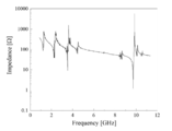
Links
Images








Classifications
-
- H—ELECTRICITY
- H03—ELECTRONIC CIRCUITRY
- H03H—IMPEDANCE NETWORKS, e.g. RESONANT CIRCUITS; RESONATORS
- H03H9/00—Networks comprising electromechanical or electro-acoustic elements; Electromechanical resonators
- H03H9/15—Constructional features of resonators consisting of piezoelectric or electrostrictive material
- H03H9/17—Constructional features of resonators consisting of piezoelectric or electrostrictive material having a single resonator
-
- H—ELECTRICITY
- H03—ELECTRONIC CIRCUITRY
- H03H—IMPEDANCE NETWORKS, e.g. RESONANT CIRCUITS; RESONATORS
- H03H9/00—Networks comprising electromechanical or electro-acoustic elements; Electromechanical resonators
- H03H9/15—Constructional features of resonators consisting of piezoelectric or electrostrictive material
- H03H9/17—Constructional features of resonators consisting of piezoelectric or electrostrictive material having a single resonator
- H03H9/171—Constructional features of resonators consisting of piezoelectric or electrostrictive material having a single resonator implemented with thin-film techniques, i.e. of the film bulk acoustic resonator [FBAR] type
-
- H—ELECTRICITY
- H03—ELECTRONIC CIRCUITRY
- H03H—IMPEDANCE NETWORKS, e.g. RESONANT CIRCUITS; RESONATORS
- H03H9/00—Networks comprising electromechanical or electro-acoustic elements; Electromechanical resonators
- H03H9/15—Constructional features of resonators consisting of piezoelectric or electrostrictive material
- H03H9/17—Constructional features of resonators consisting of piezoelectric or electrostrictive material having a single resonator
- H03H9/171—Constructional features of resonators consisting of piezoelectric or electrostrictive material having a single resonator implemented with thin-film techniques, i.e. of the film bulk acoustic resonator [FBAR] type
- H03H9/172—Means for mounting on a substrate, i.e. means constituting the material interface confining the waves to a volume
- H03H9/175—Acoustic mirrors
-
- H—ELECTRICITY
- H03—ELECTRONIC CIRCUITRY
- H03H—IMPEDANCE NETWORKS, e.g. RESONANT CIRCUITS; RESONATORS
- H03H9/00—Networks comprising electromechanical or electro-acoustic elements; Electromechanical resonators
- H03H9/02—Details
- H03H9/02007—Details of bulk acoustic wave devices
- H03H9/02015—Characteristics of piezoelectric layers, e.g. cutting angles
-
- H—ELECTRICITY
- H03—ELECTRONIC CIRCUITRY
- H03H—IMPEDANCE NETWORKS, e.g. RESONANT CIRCUITS; RESONATORS
- H03H9/00—Networks comprising electromechanical or electro-acoustic elements; Electromechanical resonators
- H03H9/02—Details
- H03H9/02007—Details of bulk acoustic wave devices
- H03H9/02015—Characteristics of piezoelectric layers, e.g. cutting angles
- H03H9/02031—Characteristics of piezoelectric layers, e.g. cutting angles consisting of ceramic
-
- H—ELECTRICITY
- H03—ELECTRONIC CIRCUITRY
- H03H—IMPEDANCE NETWORKS, e.g. RESONANT CIRCUITS; RESONATORS
- H03H9/00—Networks comprising electromechanical or electro-acoustic elements; Electromechanical resonators
- H03H9/02—Details
- H03H9/02007—Details of bulk acoustic wave devices
- H03H9/02062—Details relating to the vibration mode
-
- H—ELECTRICITY
- H03—ELECTRONIC CIRCUITRY
- H03H—IMPEDANCE NETWORKS, e.g. RESONANT CIRCUITS; RESONATORS
- H03H9/00—Networks comprising electromechanical or electro-acoustic elements; Electromechanical resonators
- H03H9/02—Details
- H03H9/125—Driving means, e.g. electrodes, coils
- H03H9/13—Driving means, e.g. electrodes, coils for networks consisting of piezoelectric or electrostrictive materials
-
- H—ELECTRICITY
- H03—ELECTRONIC CIRCUITRY
- H03H—IMPEDANCE NETWORKS, e.g. RESONANT CIRCUITS; RESONATORS
- H03H9/00—Networks comprising electromechanical or electro-acoustic elements; Electromechanical resonators
- H03H9/46—Filters
- H03H9/54—Filters comprising resonators of piezoelectric or electrostrictive material
- H03H9/56—Monolithic crystal filters
- H03H9/564—Monolithic crystal filters implemented with thin-film techniques
-
- H—ELECTRICITY
- H03—ELECTRONIC CIRCUITRY
- H03H—IMPEDANCE NETWORKS, e.g. RESONANT CIRCUITS; RESONATORS
- H03H9/00—Networks comprising electromechanical or electro-acoustic elements; Electromechanical resonators
- H03H9/46—Filters
- H03H9/54—Filters comprising resonators of piezoelectric or electrostrictive material
- H03H9/56—Monolithic crystal filters
- H03H9/566—Electric coupling means therefor
- H03H9/568—Electric coupling means therefor consisting of a ladder configuration
-
- H—ELECTRICITY
- H03—ELECTRONIC CIRCUITRY
- H03H—IMPEDANCE NETWORKS, e.g. RESONANT CIRCUITS; RESONATORS
- H03H9/00—Networks comprising electromechanical or electro-acoustic elements; Electromechanical resonators
- H03H9/46—Filters
- H03H9/54—Filters comprising resonators of piezoelectric or electrostrictive material
- H03H9/542—Filters comprising resonators of piezoelectric or electrostrictive material including passive elements
Definitions
- the present invention relates to an elastic wave device.
- the frequency band from 700 MHz to 3 GHz which is mainly used in smartphones and the like, has nearly 80 bands and is extremely congested.
- the 5th generation mobile communication system (5G) has 3 It is planned to use the frequency band from .6 GHz to 4.9 GHz, and in the next 6th generation, it is also planned to use the frequency band of 6 GHz or higher.
- an elastic surface wave (SAW) device using a LiTaO 3 crystal (LT) or a LiNbO 3 crystal (LN) as a piezoelectric thin film, or a bulk wave surface acoustic wave FBAR (thin film piezoelectric resonator; Film Bulk Acoustic Resonator) devices are used.
- bulk wave elastic wave FBAR devices using piezoelectric thin films include hollow FBARs that require cavities above and below the piezoelectric thin films, and acoustic multilayer films and holding substrates instead of cavities on one side of the piezoelectric thin films.
- the hollow type FBAR there are those using a piezoelectric thin film of AlN or ScAlN (see, for example, Non-Patent Document 1 or 2) and those using a single crystal thin plate of LN (see, for example, Non-Patent Document 3). ).
- the vibration mode of the bulk wave used is only the thickness longitudinal vibration.
- the speed of sound of this longitudinal wave is represented by (c33 D / density) 1/2 (c33 D is an elastic stiffness constant), and the excitation frequency is strictly reduced by the mass load of the electrodes, but is approximately the speed of sound / (2). ⁇ film thickness). Therefore, in order to increase the excitation frequency to a high frequency, the film thickness of the piezoelectric thin film must be extremely thin. Further, even in the hollow type FBAR using the single crystal thin plate of LN, the excitation frequency is inversely proportional to the thickness of the substrate.
- the film thickness of the piezoelectric thin film must be extremely thin.
- an excitation frequency of about 2 GHz and an impedance ratio of about 60 dB are obtained.
- the thickness of each acoustic film is set to half the thickness of the piezoelectric thin film (that is, wavelength / 4) in order to increase the excitation in the basic mode.
- This elastic wave device also has a bulk wave vibration mode of thickness longitudinal vibration, but at 3 GHz in the basic mode, an impedance ratio of only 21 dB was obtained in actual measurement, and its characteristics were inferior to those of the hollow FBAR made of AlN film. Therefore, it has not been put into practical use.
- a high resonance frequency in the acoustic multilayer film structure FBAR, assuming that a high resonance frequency can be obtained, it is composed of either ZnO or AlN between the upper and lower electrodes, and the [0001] direction is one direction substantially parallel to the surface of the piezoelectric thin film.
- Higher-order mode thin film resonator provided with a piezoelectric thin film in which an oriented first piezoelectric layer and a second piezoelectric layer oriented in a direction different from that of the first piezoelectric layer in the [0001] direction by 180 ° are overlapped.
- Patent Document 1 has been developed (see, for example, Patent Document 1). According to this resonator, the resonance frequency is doubled as compared with the conventional one having the same thickness of the piezoelectric thin film.
- the impedance ratio is lowered to 50 dB at 5 GHz and 3 GHz, respectively, and is ultra-high at 6 GHz or more. In the frequency band, there is a problem that good characteristics with a large impedance ratio cannot be obtained. Further, in the hollow type FBAR as described in Non-Patent Documents 1 to 3, the piezoelectric thin film becomes extremely thin as 0.3 to 0.6 ⁇ m in the ultra-high frequency band of 6 GHz or more, so that the mechanical strength is maintained. There was also the problem that it was difficult. In particular, the hollow type FBAR described in Non-Patent Document 3 cannot be put into practical use because the piezoelectric thin film is an LN single crystal thin plate, so that mechanical strength cannot be obtained as compared with the polycrystalline thin film.
- Patent Document 1 which is an acoustic multilayer film structure FBAR is a piezoelectric material at the same resonance frequency as compared with a hollow type FBAR using a fundamental wave as described in Non-Patent Documents 1 to 3.
- the thickness of the thin film is doubled, but the two piezoelectric layers constituting the piezoelectric thin film have the same thickness as the conventional piezoelectric thin film. Therefore, in the ultra-high frequency band of 6 GHz or more, each piezoelectric layer becomes extremely thin, and there is a problem that it is difficult to maintain these mechanical strengths.
- the piezoelectric thin film in the ultra-high frequency band of 6 GHz or more, even if the piezoelectric thin film is doubled in thickness, it is still very thin, so that it is difficult to maintain the mechanical strength of the piezoelectric thin film itself. .. Further, even when the frequency is 560 MHz, only an impedance ratio of 12 dB is obtained, and when the frequency becomes 6 GHz, the impedance ratio becomes further smaller, so that there is a problem that it is difficult to put it into practical use. Note that the acoustic multilayer film structure FBAR as described in Non-Patent Document 6 and Patent Document 1 only uses a polycrystalline piezoelectric thin film, and good characteristics are not realized even in the basic mode, and its frequency is high. It is 3 GHz or less.
- the present invention has focused on such a problem, and provides an elastic wave device capable of obtaining good characteristics and maintaining sufficient mechanical strength in an ultra-high frequency band of 6 GHz or higher.
- the purpose is to provide.
- the elastic wave device includes a piezoelectric substrate, an electrode provided in contact with the piezoelectric substrate, and an acoustic multilayer film provided in contact with the piezoelectric substrate and / or the electrode. It is characterized in that it is configured to utilize the higher-order mode of the resonance characteristics of the bulk wave.
- the elastic wave device can excite a higher-order mode (overtone) (primary mode, secondary mode, ...) With a higher frequency than the basic mode (0th order) by the acoustic multilayer film. .. Further, by adjusting the type of the piezoelectric substrate and the thickness of each layer of the acoustic multilayer film, a higher-order mode having a large impedance ratio can be obtained. By utilizing this high-order mode, the elastic wave device according to the present invention can obtain good characteristics having a large impedance ratio in an ultra-high frequency band of 6 GHz or more.
- the impedance ratio is the ratio [20 ⁇ log (Za / Zr)] of the resonance impedance Zr at the resonance frequency and the antiresonance impedance Za at the antiresonance frequency.
- the electrodes are composed of two or more. Further, the electrode may cover the entire surface of one surface of the piezoelectric substrate, or may cover a part of the piezoelectric substrate. Further, the electrode may have any shape such as a circular shape, a polygonal shape, or an elliptical shape. Further, the elastic wave device according to the present invention may have a structure in which electrodes are provided on both sides of the piezoelectric substrate, and a structure in which two resonators are connected in series, that is, between the piezoelectric substrate and the acoustic multilayer film.
- the piezoelectric substrate also includes a piezoelectric thin film and a piezoelectric thin plate.
- the low acoustic impedance film and the high acoustic impedance film are alternately laminated in the acoustic multilayer film.
- the low acoustic impedance film and the high acoustic impedance film are alternately and continuously laminated in 3 layers or more and 20 layers or less.
- the thickness of at least three layers of the low acoustic impedance film and the high acoustic impedance film of the acoustic multilayer film is preferably 0.016 wavelength to 0.11 wavelength of the bulk wave.
- the acoustic impedance film is preferably formed in a layer close to the piezoelectric substrate. Further, the acoustic multilayer film has one or more layers of the low acoustic impedance film and two or more layers of the high acoustic impedance film, and the thickness of one layer of the low acoustic impedance film or each of the two layers of low acoustic impedance. The sum of the average thickness of the film and the average thickness of each of the two high-acoustic impedance films may be 0.07 to 0.15 wavelengths of the bulk wave. As a result, the higher-order mode can be excited at a frequency about three times or more that of the basic mode.
- the wavelength of the bulk wave is defined by 2 ⁇ (thickness of the piezoelectric substrate).
- the thickness t of the piezoelectric substrate may be defined as an effective thickness (t + mt) including the average thickness mt of the electrodes on both sides of the piezoelectric substrate.
- each low acoustic impedance film and / or each high acoustic impedance film of the acoustic multilayer film is, for example, Mg alloy, SiO 2 , Al, Si, Ge, Ti, ZnO, Si x N. y, (wherein, x and y are positive real number) SiO x F y, AlN, SiC, Al 2 O 3, Ag, Hf, TiO 2, Ni, Au, Ta, Mo, Pt, W, and Cu of It is preferably composed of a film containing at least one of them, or an oxide film, a nitride film, a carbonized film or an iodide film containing at least one of them.
- the low acoustic impedance film may consist of a film having a smaller acoustic impedance than the adjacent high acoustic impedance films.
- the piezoelectric substrate is preferably composed of a single crystal of LiNbO 3 , LiTaO 3 , Li 2 B 4 O 7 , or langasite. In this case, it is easy to excite the higher-order mode.
- the c-axis oriented piezoelectric polycrystalline thin film such as AlN or ScAlN used in FBAR has a small piezoelectric constant, so that it is difficult to excite the higher-order mode.
- a single crystal piezoelectric substrate such as LiNbO 3 (LN) or LiTaO 3 (LT) has a large bonding coefficient, and unlike a polycrystalline film formed by film formation, an arbitrary azimuth angle can be used. Therefore, in addition to the thickness longitudinal vibration using the longitudinal wave of the bulk wave, the thickness slip vibration using the transverse wave can also be used.
- the Euler angles of the piezoelectric substrate are (0 ° ⁇ 5 °, 66.5) in order to obtain a large impedance ratio.
- ° -82 °, 0 ° -180 °) and (90 ° ⁇ 5 °, 90 ° ⁇ 5 °, 0 ° -180 °), or crystallographically equivalent to any one of these Euler angles are preferred, and Euler angles are more preferably (0 ° ⁇ 5 °, 70 ° -81 °, 0 ° -180 °), or crystallographically equivalent Euler angles. It is even more preferred that the angles are (0 ° ⁇ 5 °, 72 ° -78 °, 0 ° -180 °) or crystallographically equivalent Euler angles.
- the Euler angles of the piezoelectric substrate are (0 ° ⁇ 5 °, 119 ° to 133 °, 0 ° to 180) in order to obtain a large impedance ratio. °), or crystallographically equivalent Euler angles, with Euler angles (0 ° ⁇ 5 °, 123 ° to 129 °, 0 ° to 180 °), or crystallographically equivalent. More preferably, they have equivalent Euler angles.
- the piezoelectric substrate in order to obtain a large impedance ratio, the piezoelectric substrate, Euler angles (0 ° ⁇ 5 °, -123 ° ⁇ -80 ° , 0 ° to 180 °), or crystallographically equivalent Euler angles, with Euler angles (0 ° ⁇ 5 °, -112 ° to -90 °, 0 ° to 180 °), Alternatively, it is more preferable that the Euler angles are crystallographically equivalent to this.
- the piezoelectric substrates When the elastic wave device according to the present invention utilizes the thickness sliding vibration of a piezoelectric substrate made of LiTaO 3 crystals, the piezoelectric substrates have Euler angles (0 ° ⁇ 5 °, 56 ° to 56 ° to obtain) in order to obtain a large impedance ratio. 96 °, 0 ° to 180 °) and (90 ° ⁇ 5 °, 90 ° ⁇ 5 °, 0 ° to 180 °), or crystallographically equivalent Euler angles to one of these It is preferable that the Euler angles are (0 ° ⁇ 5 °, 62 ° to 93 °, 0 ° to 180 °), or crystallographically equivalent Euler angles.
- the Euler angles of the piezoelectric substrate are (0 ° ⁇ 5 °, 112 ° to 138 °, 0 ° to 180 ° to 180) in order to obtain a large impedance ratio. °), or crystallographically equivalent Euler angles.
- the Euler angles of the piezoelectric substrate are (0 ° ⁇ 5 °, 63 ° to 91 °, 0) in order to obtain a large impedance ratio. (° to 180 °) and (90 ° ⁇ 5 °, 90 ° ⁇ 5 °, 0 ° to 180 °), or crystallographically equivalent Euler angles to any one of them. preferable.
- the elastic wave device preferably has a holding substrate provided on the opposite side of the acoustic multilayer film from the piezoelectric substrate so that the acoustic multilayer film is sandwiched between the elastic wave device and the piezoelectric substrate.
- the holding substrate may be made of any material as long as it can support a piezoelectric substrate, electrodes, and an acoustic multilayer film.
- a Si substrate, a crystal substrate, a sapphire substrate, a glass substrate, a quartz substrate, a germanium substrate, and an alumina substrate It consists of and so on.
- the elastic wave device is formed by stacking two piezoelectric substrates in order to obtain a large impedance ratio, and one piezoelectric substrate has an upper surface oiler angle ( ⁇ , ⁇ , ⁇ ) and a lower surface.
- the oiler angle is ( ⁇ , ⁇ + 180 °, ⁇ )
- the oiler angle on the upper surface is ( ⁇ , ⁇ + 180 °, ⁇ )
- the oiler angle on the lower surface is ( ⁇ , ⁇ , ⁇ ), or one of the piezoelectric substrates.
- the wavelength of the bulk wave when two piezoelectric substrates are superposed is 2 ⁇ (total thickness of the two piezoelectric substrates).
- the piezoelectric substrates are formed by superimposing two sheets thereof, and one of the piezoelectric substrates has an upper surface oiler angle ( ⁇ , ⁇ , ⁇ ).
- the lower surface oiler angle is ( ⁇ , ⁇ + 180 °, ⁇ )
- the other piezoelectric substrate has the upper surface oiler angle ( ⁇ , ⁇ + 180 °, ⁇ )
- the lower surface oiler angle is ( ⁇ , ⁇ , ⁇ )
- One piezoelectric substrate has an upper surface oiler angle ( ⁇ , ⁇ , ⁇ ), a lower surface oiler angle ( ⁇ , ⁇ + 180 °, ⁇ ), and the other piezoelectric substrate has an upper surface oiler angle ( ⁇ , ⁇ + 180 °).
- the lower surface oiler angle is ( ⁇ , ⁇ , ⁇ + 180 °), or one piezoelectric substrate has an upper surface oiler angle ( ⁇ , ⁇ , ⁇ ) and a lower surface oiler angle ( ⁇ , ⁇ , ⁇ ).
- ⁇ + 180 °, ⁇ ) the oiler angle on the upper surface of the other piezoelectric substrate is ( ⁇ , ⁇ , ⁇ + 180 °), and the oiler angle on the lower surface is ( ⁇ , ⁇ + 180 °, ⁇ + 180 °), and the thickness slip vibration of the piezoelectric substrate.
- It may be configured to utilize a higher-order mode of about 3 times or about 5 times the 2nd harmonic of.
- the piezoelectric substrate may be a strip type.
- the acoustic multilayer film is formed by alternately stacking one or more low acoustic impedance films and two or more high acoustic impedance films, and one layer.
- the sum of the thickness of the low acoustic impedance film or the average thickness of each low acoustic impedance film of any two layers and the average thickness of each high acoustic impedance film of any two layers is 0.02 to 0.02 of the bulk wave. It is preferably 0.09 wavelength.
- Euler angles ( ⁇ , ⁇ , ⁇ ) are right-handed systems and represent the cut surface of the piezoelectric substrate and the propagation direction of elastic waves. That is, with respect to the crystals constituting the piezoelectric substrate and the crystal axes X, Y, and Z of LT or LN, the X axis is rotated by ⁇ counterclockwise with the Z axis as the rotation axis to obtain the X'axis. Next, the X'axis is used as the rotation axis, and the Z axis is rotated by ⁇ counterclockwise to obtain the Z'axis. At this time, the Z'axis is the normal line, and the surface including the X'axis is the cut surface of the piezoelectric substrate.
- the direction in which the Z'axis is the rotation axis and the X'axis is ⁇ -rotated counterclockwise is defined as the propagation direction of the elastic wave.
- the axes perpendicular to the X'axis and the Z'axis obtained by moving the Y axis by these rotations are defined as the Y'axis.
- an elastic wave device capable of obtaining good characteristics and maintaining sufficient mechanical strength in an ultra-high frequency band of 6 GHz or more.
- FIG. A perspective view showing an elastic wave device according to an embodiment of the present invention, (b) a side view of (a), and (c) a perspective view showing two variations of the upper electrode of the elastic wave device of (a).
- FIG. (d) side view of (c), perspective view of (e) (a) elastic wave device showing three deformation examples of upper electrodes, side view of (f) (e), (g) ( It is an equivalent circuit of e).
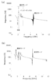
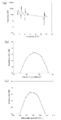
- 1 (a) and 1 (b) is a (0 °, 75 °, ⁇ ) LN substrate, and the average thickness of each layer of the acoustic multilayer film is set to the excited bulk wave ( It is a graph which shows the frequency characteristic of the thickness slip vibration at the time of a) 0.25 wavelength, (b) 0.05 wavelength.
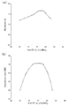
- 1 (a) and 1 (b) is a (0 °, ⁇ , ⁇ ) LN substrate and the average thickness of each layer of the acoustic multilayer film is set to 0.05 wavelength
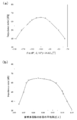
- the piezoelectric substrate of the elastic wave device shown in FIGS. 1 (a) and 1 (b) is a (0 °, 75 °, ⁇ ) LN substrate and (a) the thickness of the high acoustic impedance film is 0.0625 wavelengths.
- the graph showing the relationship between the thickness of the low acoustic impedance film and the impedance ratio of the high-order mode of the thickness sliding vibration (b) High acoustic impedance when the thickness of the low acoustic impedance film is 0.0625 wavelengths.
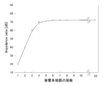
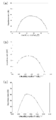
- 1 (a) and 1 (b) is a (0 °, 75 °, ⁇ ) LN substrate and the average thickness of each layer of the acoustic multilayer film is 0.05 wavelength. It is a graph which shows the relationship between the number of layers of an acoustic multilayer film, and the impedance ratio of the high-order mode of a thickness sliding vibration. The average thickness of each layer of the acoustic multilayer film and the height of the thickness slip vibration when the piezoelectric substrate of the elastic wave device shown in FIGS. 1 (a) and 1 (b) is the (90 °, 90 °, ⁇ ) LN substrate. It is a graph which shows the relationship with the impedance ratio of the next mode.
- the (a) piezoelectric substrate of the elastic wave device shown in FIGS. 1 (a) and 1 (b) is a (0 °, 126 °, ⁇ ) LN substrate, and the average thickness of each layer of the acoustic multilayer film is set to 0.05 wavelength.
- the piezoelectric substrate (a) of the elastic wave device shown in FIGS. 1 (a) and 1 (b) is the LT substrate of (0 °, ⁇ , ⁇ ), and the average thickness of each layer of the acoustic multilayer film is set to 0.05 wavelength.
- 2 (a) and 2 (b) is a (0 °, ⁇ , ⁇ ) LT substrate, and the average thickness of each layer of the acoustic multilayer film is 0.05.
- a graph showing the ⁇ dependence of the impedance ratio in the higher-order mode of thickness slip vibration when the wavelength is set
- Acoustic multilayer film when the piezoelectric substrate is an LT substrate (0 °, 74 °, 175 °).
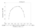
- the average thickness and two layers of any two layers of low acoustic impedance film when the piezoelectric substrate of the elastic wave device shown in FIGS. 1 (a) and 1 (b) is a (90 °, 90 °, ⁇ ) LN substrate.
- the piezoelectric substrate of the elastic wave device shown in FIG. 14 is a (0 °, 126 °, ⁇ ) LN substrate (0 °, 306 °, ⁇ ) / (0 °, 306 °, ⁇ ) LN substrate (0 °, 126 °). , ⁇ ), it is a graph which shows the frequency characteristic of the thickness longitudinal vibration.
- the piezoelectric substrate of the elastic wave device shown in FIG. 14 is a (0 °, 126 °, ⁇ ) LN substrate (0 °, 306 °, ⁇ ) / (0 °, 306 °, ⁇ ) LN substrate (0 °, 126 °).
- the piezoelectric substrate is (0 °, 126 °, ⁇ ) LN substrate (0 °, 306 °, ⁇ ) / (0 °, 306 °, ⁇ + 180 °) LN substrate (0 °, 126 °) °, ⁇ + 180 °), and (a) low when the piezoelectric substrate of the elastic wave device shown in FIGS. 1 (a) and 1 (b) is the (0 °, 126 °, ⁇ ) LN substrate.
- the piezoelectric substrate of the elastic wave device shown in FIG. 14 is a (0 °, 74 °, 0 °) LN substrate (0 °, 254 °, 0 °) / (0 °, 254 °, 0 °) LN substrate (0 °).
- the elastic wave device 10 is configured to utilize the higher-order mode of the resonance characteristics of the bulk wave, and is configured to utilize the piezoelectric substrate 11, the electrode 12, the acoustic multilayer film 13, and the holding substrate. It has 14.
- the piezoelectric substrate 11 is made of a single crystal of LiNbO 3 , LiTaO 3 , Li 2 B 4 O 7 , or langasite.
- the electrode 12 is composed of two or more electrodes, each of which has a thin plate shape. Each electrode 12 is attached to one surface or the other surface of the piezoelectric substrate 11 along the surface of the piezoelectric substrate 11. Each electrode 12 may be provided so as to cover the entire surface of the piezoelectric substrate 11, or may be provided so as to cover a part of the surface of the piezoelectric substrate 11. Further, each electrode 12 may have any planar shape, may be circular as shown in FIG. 1 (a), or may be rectangular as shown in FIGS. 1 (c) and 1 (e). There may be.
- the electrodes 12 are composed of a pair, each of which is one surface of the piezoelectric substrate 11. And may be provided on the other surface. Further, as shown in FIGS. 1 (c), 1 (d), 2 (c), and (d), the electrode 12 is composed of three electrodes, and the two resonators are connected in series. One electrode 12 may be provided as a common electrode so as to cover one surface of the piezoelectric substrate 11, and the remaining two electrodes 12 may be provided side by side on the other surface of the piezoelectric substrate 11. Further, as shown in FIGS.
- the electrode 12 is composed of four electrodes and has a structure in which three resonators are connected in series or in parallel.
- One electrode 12 may be provided as a common electrode so as to cover one surface of the piezoelectric substrate 11, and the remaining three electrodes 12 may be provided side by side on the other surface of the piezoelectric substrate 11. Further, the number of these electrodes 12 may be further increased.
- the acoustic multilayer film 13 is attached to the surface of the electrode 12 provided on one surface of the piezoelectric substrate 11 on the side opposite to the piezoelectric substrate 11.
- the acoustic multilayer film 13 low acoustic impedance films 13a and high acoustic impedance films 13b are alternately laminated from the side of the piezoelectric substrate 11 to the opposite side.
- the low acoustic impedance film 13a and the high acoustic impedance film 13b are alternately and continuously laminated in 3 layers or more and 20 layers or less. In a specific example shown in FIGS.
- the layer closest to the piezoelectric substrate 11 is the low acoustic impedance film 13a, and the low acoustic impedance film 13a and the high acoustic impedance film 13b are alternately and continuously laminated in six layers. Has been done.
- Each low acoustic impedance film 13a and each high acoustic impedance film 13b is a film containing at least one of the materials shown in Table 1 or Table 2, or a film containing at least one of the materials shown in Table 1 or Table 2, regardless of whether the bulk wave longitudinal wave or transverse wave is used. It is composed of an oxide film, a nitride film, a carbide film or an iodide film containing at least one of them.
- Zl is the acoustic impedance of the longitudinal wave of the bulk wave
- c33 is the elastic stiffness constant
- Zs in Table 2 is the acoustic impedance of the transverse wave of the bulk wave
- c44 is the elastic stiffness constant.
- x and y of Si x N y in Tables 1 and 2 are positive real numbers.
- Each low acoustic impedance film 13a is made of one having a smaller acoustic impedance than the adjacent high acoustic impedance film 13b.
- Each low acoustic impedance film 13a may be made of the same material, but may be made of different materials.
- each high acoustic impedance film 13b may be made of the same material, but may be made of different materials.
- each low acoustic impedance film 13a is made of an Al film
- each high acoustic impedance film 13b is made of a W film.
- the holding substrate 14 is attached to the surface of the acoustic multilayer film 13 opposite to the piezoelectric substrate 11 so as to sandwich the acoustic multilayer film 13 with the piezoelectric substrate 11.
- the holding substrate 14 is provided to support the piezoelectric substrate 11, the electrodes 12, and the acoustic multilayer film 13.
- the holding substrate 14 is made of a Si substrate, but is also made of a crystal substrate, a sapphire substrate, a glass substrate, a quartz substrate, a germanium substrate, an alumina substrate, and the like. May be.
- the elastic wave device 10 may have a pair of electrodes 12. Further, as shown in FIGS. 1 (c) and 1 (d), two electrodes (upper electrodes) 12 and the piezoelectric substrate 11 are provided on the other surface of the piezoelectric substrate 11, that is, the surface opposite to the acoustic multilayer film 13. A structure in which one electrode (lower electrode) 12 is provided on one surface and two resonators are connected in series may be formed. In this case, the multiple mode filter can be configured by using the upper electrode 12 as the input / output electrode and the lower electrode 12 as the ground common electrode.
- the elastic wave device 10 may have an elongated strip type structure as shown in FIG.
- the other surface of the piezoelectric substrate 11, that is, the side surface on the long side of the electrode 12 provided on the surface opposite to the acoustic multilayer film 13, is aligned with the position of the side surface of the piezoelectric substrate 11. Is formed.
- the electrodes 12 may be composed of a pair.
- two electrodes (upper electrodes) 12 are provided on the other surface of the piezoelectric substrate 11, and an electrode (lower electrode) 12 is provided on one surface of the piezoelectric substrate 11.
- a structure may be formed in which two resonators provided with one are connected in series.
- the multiple mode filter can be configured by using the upper electrode 12 as the input / output electrode and the lower electrode 12 as the ground common electrode.
- one end of the piezoelectric substrate 11 to the acoustic multilayer film 13 is provided on a pair of opposite side edges so that the width between the side edges is narrowed.
- a strip-shaped structure may be formed by making an elongated groove-shaped (rectangular) notch 15 leaving the other end portion.
- the elastic wave device 10 is provided with three upper electrodes 12 and one lower electrode, and these electrodes are provided. 12 may be connected to form a structure.
- the three upper electrodes 12 as the input electrode, the output electrode, and the ground common electrode of the filter, respectively, and the lower electrode 12 as the common electrode connecting the three resonators, FIGS. 1 (g) and FIG.
- the T-type ladder filter shown by the equivalent circuit of FIG. 2 (i) can be configured.
- a ladder filter having a larger number of stages can be configured.
- the elastic wave device 10 shown in FIG. 1 can utilize the thickness sliding vibration of the piezoelectric substrate 11 or the thickness longitudinal vibration of the piezoelectric substrate 11.
- the elastic wave device 10 shown in FIG. 2 can utilize the thickness sliding vibration of the piezoelectric substrate 11.
- the elastic wave device 10 can excite a higher-order mode (primary mode, secondary mode, ...) With a higher frequency than the basic mode (0th order) by the acoustic multilayer film 13. Further, by adjusting the type of the piezoelectric substrate 11 and the thickness of each layer of the acoustic multilayer film 13, a higher-order mode having a large impedance ratio can be obtained. By utilizing this high-order mode, the elastic wave device 10 can obtain good characteristics having a large impedance ratio in an ultra-high frequency band of 6 GHz or more.
- the M axis is the Y axis when the piezoelectric substrate is ( ⁇ 90 °, ⁇ 90 °, ⁇ ), and the X axis when the piezoelectric substrate is other Euler angles. Is shown. Further, ⁇ is an angle with respect to the direction N perpendicular to the plane in contact with the rotated M-axis counterclockwise from the M-axis, as shown in FIGS. 1 (a) and 2 (a).
- the frequency characteristics of the thickness slip vibration and the impedance ratio in the higher-order mode were determined by using the piezoelectric substrate 11 of the LN substrate.
- the electrode 12 (hereinafter referred to as "upper electrode") provided on the other surface of the piezoelectric substrate 11, that is, the surface opposite to the acoustic multilayer film 13, is used as an Al electrode (thickness 50 nm), and the piezoelectric substrate 11 is an oiler.
- an LN substrate (thickness 1 ⁇ m) with angles (0 °, 75 °, ⁇ ) is used, and the electrode 12 (hereinafter referred to as “lower electrode”) between the piezoelectric substrate 11 and the acoustic multilayer film 13 is an Al electrode (thickness 50 nm). ). Further, the acoustic multilayer film 13 was formed by alternately laminating 6 layers of a low acoustic impedance film 13a of an Al film and a high acoustic impedance film 13b of a W film, and the holding substrate 14 was a Si substrate.
- the thicknesses of both the Al electrode of the lower electrode and the Al film of the first layer low acoustic impedance film 13a are distinguished, but when both are made of the same material, the total film thickness of both is used.
- the thickness of the low acoustic impedance film 13a may be set.
- the electrode 12 uses an Al electrode having a low density and a thin thickness of 50 nm as the upper electrode in order to suppress a decrease in frequency due to a mass load.
- Euler angles ( ⁇ , ⁇ , ⁇ ) are simply represented by ( ⁇ , ⁇ , ⁇ ).
- FIG. 3A shows the frequency characteristics when the average thickness of each layer of the acoustic multilayer film 13 is 0.25 wavelength of the excited bulk wave (half the thickness of the piezoelectric substrate 11).
- the basic resonance frequency (basic mode) of the thickness slip vibration of 1.9 GHz was strongly excited and an impedance ratio of 73 dB was obtained.
- the impedance ratio of the higher-order mode of 6.9 GHz which is about 3.6 times that of the basic mode, is about 40 dB.
- FIG. 3 (b) shows the frequency characteristics when the average thickness of each layer of the acoustic multilayer film 13 is set to 1/5 of FIG. 3 (a), that is, 0.05 wavelength.
- FIG. 3 (b) it was confirmed that the resonance characteristic of the high-order mode frequency of 6.9 GHz was strongly excited and an impedance ratio of 72 dB was obtained. This is about the same as the impedance ratio of 73 dB in the basic mode of FIG. 3 (a). Further, it was confirmed that the excitation in the 1 to 2 GHz band of the basic mode was divided into three, the impedance ratio of each was suppressed to 17 dB or less, and the influence as spurious was small.
- the piezoelectric substrate 11 is a (0 °, ⁇ , ⁇ ) LN substrate and the average thickness of each layer of the acoustic multilayer film 13 is 0.05 wavelength, the band width of the higher-order mode of about 7 GHz.
- the ⁇ dependence of the impedance ratio are shown in FIGS. 4 (a) and 4 (b), respectively.
- the impedance ratio of the low acoustic impedance film 13a is 50 dB or more at 0.016 wavelength to 0.11 wavelength, 60 dB or more at 0.026 wavelength to 0.10 wavelength, and 0. It was confirmed that 70 dB or more can be obtained at a wavelength of .0375 to 0.09.
- the piezoelectric substrate 11 is a (0 °, 75 °, ⁇ ) LN substrate and the thickness of the low acoustic impedance film 13a is 0.0625 wavelength
- the thickness of the high acoustic impedance film 13b and about 7 GHz
- the impedance ratio of the high acoustic impedance film 13b is 50 dB or more at 0.016 wavelength to 0.107 wavelength, 60 dB or more at 0.025 wavelength to 0.10 wavelength, and 0. It was confirmed that 70 dB or more can be obtained at a wavelength of .038 to 0.08.
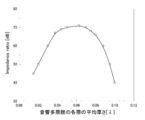
- the relationship between the average thickness of each layer of the acoustic multilayer film 13 and the impedance ratio in the higher-order mode of about 7 GHz when the piezoelectric substrate 11 is a (0 °, 75 °, ⁇ ) LN substrate is obtained and shown in FIG. It is shown in 5 (c).
- the impedance ratio is 50 dB or more when the average thickness of each layer of the acoustic multilayer film 13 is 0.023 wavelength to 0.097 wavelength or more, and 60 dB or more when 0.032 wavelength to 0.087 wavelength. , It was confirmed that 70 dB or more can be obtained at 0.043 wavelength to 0.07 wavelength.
- the acoustic multilayer film 13 is used.
- the average thickness of the six layers of the film 13 is 0.7 wavelength.
- the average thickness of each layer of the acoustic multilayer film 13 is the average thickness from the side of the piezoelectric substrate 11 to the third or fourth layer, or any continuous three layers in the acoustic multilayer film 13. It may be calculated by the average thickness of four layers.
- a very thin multilayer electrode 12 When a very thin multilayer electrode 12 is used as the electrode 12 in the vicinity of the first layer, it may not act as the acoustic multilayer film 13 because it acts as the electrode 12. Further, the electrode 12 that can serve as both the electrode 12 and the acoustic impedance film, such as the Al electrode, can be included as a layer of the acoustic multilayer film 13.
- the relationship between the average thickness of each layer of the acoustic multilayer film 13 and the impedance ratio in the higher-order mode of about 7 GHz when the piezoelectric substrate 11 is a (90 °, 90 °, ⁇ ) LN substrate is obtained and shown in FIG. Shown in 7.
- the impedance ratio is such that the average thickness of each layer of the acoustic multilayer film 13 is 50 dB or more at 0.02 wavelength to 0.095 wavelength, 60 dB or more at 0.03 wavelength to 0.088 wavelength, and 0. It was confirmed that 70 dB or more can be obtained at 05 wavelength to 0.07 wavelength.
- the frequency characteristics of the thickness longitudinal vibration and the impedance ratio of the higher-order mode were determined by using the piezoelectric substrate 11 of the LN substrate.
- the upper electrode was an Al electrode (thickness 50 nm)
- the piezoelectric substrate 11 was a (0 °, 126 °, ⁇ ) LN substrate (thickness 1 ⁇ m)
- the lower electrode was an Al electrode (thickness 50 nm).
- the acoustic multilayer film 13 was formed by alternately laminating 6 layers of a low acoustic impedance film 13a of an Al film and a high acoustic impedance film 13b of a W film, and the holding substrate 14 was a Si substrate.
- FIG. 8A shows the frequency characteristics when the average thickness of each layer of the acoustic multilayer film 13 is set to 0.05 wavelength.
- the resonance characteristic of the frequency of 11 GHz which is about 1.6 times that of the high-order mode of the thickness slip vibration of FIG. 3 (b)
- an impedance ratio of 63 dB was obtained.
- the difference in frequency in the higher-order mode is due to the difference between the sound velocity of the transverse wave and the sound velocity of the longitudinal wave of the bulk wave. From these results, it can be seen that the use of the higher-order mode of thickness longitudinal vibration can realize a device with a higher frequency, although the impedance ratio is lower.
- the relationship with the impedance ratio was obtained and shown in FIG. 8 (c).
- the impedance ratio is 50 dB or more when the average thickness of each layer of the acoustic multilayer film 13 is 0.032 wavelength to 0.08 wavelength, and 60 dB or more when 0.043 wavelength to 0.07 wavelength. It was confirmed that it could be obtained.
- the impedance ratio of the higher-order mode of the thickness slip vibration was determined by using the piezoelectric substrate 11 of the LN substrate.
- the upper electrode was an Al electrode (thickness 50 nm)
- the piezoelectric substrate 11 was a (0 °, ⁇ , 18 °) LN substrate (thickness 1 ⁇ m)
- the lower electrode was an Al electrode (thickness 50 nm).
- the acoustic multilayer film 13 was formed by alternately laminating 6 layers of a low acoustic impedance film 13a of an Al film and a high acoustic impedance film 13b of a W film, and the holding substrate 14 was a Si substrate.
- FIG. 9A shows the ⁇ dependence of the impedance ratio in the higher-order mode when the average thickness of each layer of the acoustic multilayer film 13 is set to 0.05 wavelength.
- ⁇ is represented by 18 °
- the average thickness of each layer of the acoustic multilayer film 13 and the impedance of the higher-order mode when the piezoelectric substrate 11 is a (0 °, -100 °, 18 °) LN substrate was obtained and shown in FIG. 9 (b).
- the impedance ratio is 50 dB or more when the average thickness of each layer of the acoustic multilayer film 13 is 0.02 wavelength to 0.1 wavelength, and 60 dB or more when 0.025 wavelength to 0.088 wavelength. It was confirmed that it could be obtained.
- the impedance ratio of the higher-order mode of the thickness slip vibration was determined by using the piezoelectric substrate 11 of the LT substrate.
- the upper electrode was an Al electrode (thickness 50 nm)
- the piezoelectric substrate 11 was an LT substrate (thickness 1 ⁇ m) of (0 °, ⁇ , ⁇ )
- the lower electrode was an Al electrode (thickness 50 nm).
- the acoustic multilayer film 13 was formed by alternately laminating 6 layers of a low acoustic impedance film 13a of an Al film and a high acoustic impedance film 13b of a W film, and the holding substrate 14 was a Si substrate.
- the relationship with the impedance ratio of the mode was obtained and shown in FIG. 10 (b).
- the impedance ratio is 50 dB or more when the average thickness of each layer of the acoustic multilayer film 13 is 0.02 wavelength to 0.083 wavelength, and 60 dB or more when 0.033 wavelength to 0.075 wavelength. It was confirmed that it could be obtained.
- the piezoelectric substrate 11 is a (90 °, 90 °, ⁇ ) LT substrate
- the relationship between the average thickness of each layer of the acoustic multilayer film 13 and the impedance ratio in the higher-order mode of about 6.1 GHz is obtained.
- FIG. 10 (c) the impedance ratio is 50 dB or more when the average thickness of each layer of the acoustic multilayer film 13 is 0.023 wavelength to 0.088 wavelength or more, and 60 dB or more when 0.036 wavelength to 0.07 wavelength. It was confirmed that it could be obtained.
- the impedance ratio of the high-order mode of the thickness longitudinal vibration was determined by using the piezoelectric substrate 11 of the LT substrate.
- the upper electrode was an Al electrode (thickness 50 nm)
- the piezoelectric substrate 11 was a (0 °, ⁇ , ⁇ ) LT substrate (thickness 1 ⁇ m)
- the lower electrode was an Al electrode (thickness 50 nm).
- the acoustic multilayer film 13 was formed by alternately laminating 6 layers of a low acoustic impedance film 13a of an Al film and a high acoustic impedance film 13b of a W film, and the holding substrate 14 was a Si substrate.
- the relationship with the impedance ratio was obtained and shown in FIG. 11 (b).
- FIG. 11B it was confirmed that the impedance ratio was 50 dB or more when the average thickness of each layer of the acoustic multilayer film 13 was 0.037 wavelength to 0.07 wavelength.
- the impedance ratio of the higher-order mode of the thickness slip vibration was determined by using the piezoelectric substrate 11 of the LT substrate.
- the upper electrode was an Al electrode (thickness 50 nm)
- the piezoelectric substrate 11 was a (0 °, ⁇ , ⁇ ) LT substrate (thickness 1 ⁇ m)
- the lower electrode was an Al electrode (thickness 50 nm).
- the acoustic multilayer film 13 was formed by alternately laminating 6 layers of a low acoustic impedance film 13a of an Al film and a high acoustic impedance film 13b of a W film, and the holding substrate 14 was a Si substrate.
- the relationship with the impedance ratio of is obtained and shown in FIG. 12 (b).
- the impedance ratio is 50 dB or more when the average thickness of each layer of the acoustic multilayer film 13 is 0.02 wavelength to 0.08 wavelength, and 55 dB or more when the average thickness is 0.03 wavelength to 0.07 wavelength. It was confirmed that it could be obtained.
- ⁇ is represented by 175 °
- the piezoelectric substrate 11 is a (90 °, 90 °, ⁇ ) LN substrate
- the acoustic multilayer film 13 is laminated with four layers of the low acoustic impedance film 13a of the SiO 2 film and the high acoustic impedance film 13b of the Ta film alternately.
- the relationship between the sum of the average thickness of the two layers of low acoustic impedance film 13a and the average thickness of the two layers of high acoustic impedance film 13b and the impedance ratio is determined and shown in FIG.
- the impedance ratio is 60 dB or more at a sum thickness of 0.07 to 0.15 wavelength, 65 dB or more at 0.083 to 0.142 wavelength, and 0.1 to 0.13 wavelength. It was confirmed that 70 dB or more could be obtained.
- This relationship can also be applied to the azimuth angle, thickness slip, and thickness longitudinal vibration of LN and LT shown in FIGS. 5 and 7 to 12, and a large impedance ratio can be obtained at 0.07 to 0.15 wavelengths.
- 0.083 to 0.142 wavelengths give a larger impedance ratio
- 0.1 to 0.13 wavelengths give a larger impedance ratio.
- the piezoelectric substrate 11 is a single plate, but as shown in FIG. 14, the piezoelectric substrate 11 is two piezoelectric substrates 11a and 11b. May be made by pasting together.
- the piezoelectric substrate 11 includes a piezoelectric substrate 11a made of a (0 °, 126 °, ⁇ ) LN substrate (thickness 1 ⁇ m) and a (0 °, 306 °, ⁇ ) LN substrate (thickness 1 ⁇ m).
- a SiO 2 film is formed below the lower electrode.
- the structure of the two bonded piezoelectric substrates 11a and 11b is (0 °, 126 °, ⁇ ) LN substrate (0 °, 306 °, ⁇ ) / (0 °, 306 °).
- ⁇ ) LN substrate (0 °, 126 °, ⁇ ) is a combination.
- the + Z direction is the + plane
- (0 °, ⁇ 90 ° to 90 °, ⁇ ) is the + plane of the LN substrate
- (0 °, 90 ° to 270 °, ⁇ ) is the ⁇ plane.
- Each of the + and-planes has a period of ⁇ of 360 °.
- This structure has a ZnO film having a [0001] orientation (corresponding to (0 °, 0 °, ⁇ )) and a [000-1] orientation (corresponding to (0 °, 180 °, ⁇ )) in Patent Document 1.
- the substrate material and azimuth are different from the structure in which the ZnO film is superposed.
- Alignment film corresponds to (0 °, 180 °, ⁇ ), ⁇ is not determined, and there are no + and-in the X and Y directions.
- the polycrystalline thin film is significantly different from the single crystal thin film.
- the [1000] film being ( ⁇ , -90 °, 0 °) and the [-1000] film being ( ⁇ , 90 °, 0 °).
- ⁇ is not determined, and there are no + or-in the X and Y directions. Therefore, even in this orientation, it is significantly different from the single crystal sheet.
- the piezoelectric substrate 11 is composed of a (0 °, 126 °, ⁇ ) LN substrate (thickness 2 ⁇ m), and Al electrodes (thickness 100 nm) are provided above and below the piezoelectric substrate 11 as electrodes 12.
- the acoustic multilayer film 13 six layers of the low acoustic impedance film 13a (thickness 100 nm) of the SiO 2 film and the high acoustic impedance film 13b (thickness 100 nm) of the Ta film are alternately formed under the lower electrode.
- the structure is such that a Si substrate is bonded to the lowermost Ta film as a holding substrate 14.
- the structure shown in FIG. 14 is the above structure.
- the overtone (higher-order mode) of the structure shown in FIG. 1A is about three times that of the basic mode, and the overtone (higher-order mode) of about three times the double wave of the structure shown in FIG.
- the frequency characteristics are shown in FIGS. 16 (a) and 16 (b), respectively.
- FIG. 16A when one piezoelectric substrate 11 is used, an impedance ratio of 63 dB can be obtained at 4.8 GHz, whereas as shown in FIG. 16B, the piezoelectric substrate 11 is 2. It was confirmed that when composed of sheets, a larger impedance ratio of 75 dB was obtained at 9.8 GHz. Further, in the structure shown in FIG. 1A, ripples exist in the band as shown in FIG.
- Structure A In the structure shown in FIG. 14, the piezoelectric substrate 11 is a (0 °, 126 °, ⁇ ) LN substrate (0 °, 306 °, ⁇ ) / (0 °, 306 °, ⁇ ) LN substrate (0 °, In the case of 126 °, ⁇ ) and a total thickness of 2 ⁇ m
- B structure In the structure shown in FIG. 14, the piezoelectric substrate 11 is (0 °, 126 °, ⁇ ) LN substrate (0 °, 306 °, ⁇ ).
- the impedance ratio is such that the thickness of the low acoustic impedance film 13a is 60 dB or more at 0.005 to 0.05 wavelengths and 65 dB or more at 0068 to 0.041 wavelengths. It was confirmed that 70 dB or more could be obtained at a wavelength of 0.009 to 0.035. Further, although not shown, when the thickness of the low acoustic impedance film 13a is set to 0.04 wavelength and the thickness of the high acoustic impedance film 13b is changed, the impedance ratio of the high acoustic impedance film 13b is similarly changed. It was confirmed that the thickness was 60 dB or more at 0.005 to 0.05 wavelength, 65 dB or more at 0.0068 to 0.041 wavelength, and 70 dB or more at 0.009 to 0.035 wavelength.
- the impedance ratio of the low acoustic impedance film 13a was 60 dB or more at a wavelength of 0.008 to 0.04 wavelength. Further, although not shown, when the thickness of the low acoustic impedance film 13a is set to 0.04 wavelength and the thickness of the high acoustic impedance film 13b is changed, the impedance ratio of the high acoustic impedance film 13b is similarly changed. It was confirmed that 60 dB or more can be obtained at a thickness of 0.008 to 0.04 wavelength. Further, it was confirmed that the A structure obtained an impedance ratio about 12 dB larger than that of the C structure, and the B structure obtained an impedance ratio of about the same size as the C structure.
- the sum of the average thickness of the low acoustic impedance film 13a and the average thickness of the high acoustic impedance film 13b is 0.02 to 0.09. It was confirmed that 60 dB or more was obtained at a wavelength of 60 dB or more, 65 dB or more at a wavelength of 0.028 to 0.085, and 70 dB or more at a wavelength of 0.04 to 0.08. Further, in the case of the B structure, it was confirmed that the sum of the impedance ratios was 60 dB or more at a wavelength of 0.034 to 0.082.
- the A structure obtained an impedance ratio about 14 dB larger than that of the C structure
- the B structure obtained an impedance ratio about the same as that of the C structure.
- the optimum thickness of the low acoustic impedance film 13a and the high acoustic impedance film 13b in the A structure and the B structure is the same for combinations other than the SiO 2 film and the Ta film.
- the (0 °, 126 °, ⁇ ) LN substrate (0 °, 306 °, ⁇ ) / (0 °, 126 °, ⁇ + 180 °) LN substrate (0 °, 306 °) It has been confirmed that the structure having a total thickness of 2 ⁇ m at °, ⁇ + 180 °) exhibits the same characteristics as the B structure.
- results shown in FIGS. 15 to 17 can be applied to double waves of other thickness longitudinal vibrations on the LN substrate and the LT substrate. That is, in the case of ( ⁇ , ⁇ , ⁇ ) (LN substrate or LT substrate) ( ⁇ , ⁇ + 180 °, ⁇ ) / ( ⁇ , ⁇ + 180 °, ⁇ ) (LN substrate or LT substrate) ( ⁇ , ⁇ , ⁇ ), In the case of ( ⁇ , ⁇ , ⁇ ) (LN substrate or LT substrate) ( ⁇ , ⁇ + 180 °, ⁇ ) / ( ⁇ , ⁇ + 180 °, ⁇ + 180 °) (LN substrate or LT substrate) ( ⁇ , ⁇ , ⁇ + 180 °) And ( ⁇ , ⁇ , ⁇ ) (LN substrate or LT substrate) ( ⁇ , ⁇ + 180 °, ⁇ ) / ( ⁇ , ⁇ , ⁇ + 180 °) (LN substrate or LT substrate) ( ⁇ , ⁇ + 180 °)
- the structure of the piezoelectric substrate 11 examined is the following six types.
- Each of the five structures D to H is a stack of two 1 ⁇ m-thick LN substrates.
- the upper and lower electrodes 12 of the piezoelectric substrate 11 are formed of an Al electrode having a thickness of 100 nm, an acoustic multilayer film 13, and a SiO 2 film of a low acoustic impedance film 13a and a Ta film of a high acoustic impedance film 13b.
- the holding substrate 14 is a Si substrate, which is obtained by alternately stacking 6 layers.
- FIG. 18 shows the relationship between the sum of the average thickness of the low acoustic impedance film 13a and the average thickness of the high acoustic impedance film 13b and the impedance ratio in the six cases of the D structure to the I structure.
- the impedance ratio is such that the sum of the average thickness of the low acoustic impedance film 13a and the average thickness of the high acoustic impedance film 13b is 60 dB or more at a wavelength of 0.045 to 0.073. It was confirmed that 65 dB or more was obtained at a wavelength of 0.0456 to 0.072, 70 dB or more at a wavelength of 0.046 to 0.069, and 75 dB or more at a wavelength of 0.049 to 0.063.
- the sum of the impedance ratios was 55 dB or more at the 0.047 to 0.065 wavelength and 60 dB or more at the 0.05 to 0.062 wavelength.
- the sum of the impedance ratios is 60 dB or more at 0.046 to 0.06 wavelength, 65 dB or more at 0.047 to 0.058 wavelength, and 70 dB or more at 0.049 to 0.0563 wavelength. It was confirmed that it could be obtained. Further, it was confirmed that in the G structure and the H structure, the impedance ratio was 50 dB or less, and good characteristics could not be obtained.
- the acoustic multilayer film 13 was examined with 6 layers, the same characteristics are exhibited if there are 3 or more layers.
- the impedance ratios of the D structure and the F structure were larger than those of the I structure by about 15 dB and 8 dB, respectively. It was confirmed that the E structure can obtain an impedance ratio similar to that of the I structure. Further, the thickness when standardized by the wavelength of each film of the acoustic multilayer film 13 having the D structure to the F structure (the wavelength is twice the thickness of the piezoelectric substrate 11) is half that of the I structure. Was also confirmed.
- the results shown in FIG. 18 can also be applied to the thickness sliding vibrations of the LN substrate and the LT substrate, the strip type thickness sliding vibrations, and the structures of FIGS. 1 and 2. That is, in the D structure, ( ⁇ , ⁇ , ⁇ ) (LN substrate or LT substrate) ( ⁇ , ⁇ + 180 °, ⁇ ) / ( ⁇ , ⁇ + 180 °, ⁇ ) (LN or LT) ( ⁇ , ⁇ , ⁇ ), In the E structure, ( ⁇ , ⁇ , ⁇ ) (LN substrate or LT substrate) ( ⁇ , ⁇ + 180 °, ⁇ ) / ( ⁇ , ⁇ + 180 °, ⁇ + 180 °) (LN substrate or LT substrate) ( ⁇ , ⁇ , ⁇ + 180 °) ), In the F structure, ( ⁇ , ⁇ , ⁇ ) (LN substrate or LT substrate) ( ⁇ , ⁇ + 180 °, ⁇ ) / ( ⁇ , ⁇ , ⁇ + 180 °) (LN substrate or LT substrate
Landscapes
- Physics & Mathematics (AREA)
- Acoustics & Sound (AREA)
- Chemical & Material Sciences (AREA)
- Crystallography & Structural Chemistry (AREA)
- Engineering & Computer Science (AREA)
- Ceramic Engineering (AREA)
- Surface Acoustic Wave Elements And Circuit Networks Thereof (AREA)
- Piezo-Electric Or Mechanical Vibrators, Or Delay Or Filter Circuits (AREA)
Priority Applications (3)
| Application Number | Priority Date | Filing Date | Title |
|---|---|---|---|
| JP2021537314A JP7527604B2 (ja) | 2019-08-08 | 2020-08-04 | 弾性波デバイス |
| CN202080056332.5A CN114375544A (zh) | 2019-08-08 | 2020-08-04 | 弹性波器件 |
| US17/633,432 US20220294415A1 (en) | 2019-08-08 | 2020-08-04 | Elastic wave device |
Applications Claiming Priority (2)
| Application Number | Priority Date | Filing Date | Title |
|---|---|---|---|
| JP2019-145908 | 2019-08-08 | ||
| JP2019145908 | 2019-08-08 |
Publications (1)
| Publication Number | Publication Date |
|---|---|
| WO2021025004A1 true WO2021025004A1 (ja) | 2021-02-11 |
Family
ID=74502981
Family Applications (1)
| Application Number | Title | Priority Date | Filing Date |
|---|---|---|---|
| PCT/JP2020/029759 Ceased WO2021025004A1 (ja) | 2019-08-08 | 2020-08-04 | 弾性波デバイス |
Country Status (4)
| Country | Link |
|---|---|
| US (1) | US20220294415A1 (https=) |
| JP (1) | JP7527604B2 (https=) |
| CN (1) | CN114375544A (https=) |
| WO (1) | WO2021025004A1 (https=) |
Cited By (3)
| Publication number | Priority date | Publication date | Assignee | Title |
|---|---|---|---|---|
| JP2023137104A (ja) * | 2022-03-17 | 2023-09-29 | 太陽誘電株式会社 | 弾性波デバイス、フィルタ、およびマルチプレクサ |
| JP2023139785A (ja) * | 2022-03-22 | 2023-10-04 | リバーエレテック株式会社 | 弾性波素子及びそれを用いた原子発振器 |
| WO2025211111A1 (ja) * | 2024-04-01 | 2025-10-09 | 株式会社村田製作所 | 弾性波フィルタ、マルチプレクサ、高周波フロントエンド回路及び通信装置 |
Citations (7)
| Publication number | Priority date | Publication date | Assignee | Title |
|---|---|---|---|---|
| JPH09162683A (ja) * | 1995-12-06 | 1997-06-20 | Matsushita Electric Ind Co Ltd | 圧電共振子 |
| JP2005051447A (ja) * | 2003-07-31 | 2005-02-24 | Tdk Corp | 圧電共振器およびそれを用いたフィルタならびに電子部品 |
| WO2013031748A1 (ja) * | 2011-09-01 | 2013-03-07 | 株式会社村田製作所 | 圧電バルク波装置及びその製造方法 |
| JP2013528996A (ja) * | 2010-04-23 | 2013-07-11 | テクノロジアン テュトキムスケスクス ヴェーテーテー | 広帯域音響結合薄膜bawフィルタ |
| JP2013225945A (ja) * | 2010-01-28 | 2013-10-31 | Murata Mfg Co Ltd | チューナブルフィルタ |
| JP2015502065A (ja) * | 2011-11-11 | 2015-01-19 | テクノロジアン テュトキムスケスクス ヴェーテーテーTeknologian tutkimuskeskus VTT | 向上した通過帯域特性を有する、横方向に結合されたバルク弾性波フィルタ |
| JP2018110317A (ja) * | 2016-12-29 | 2018-07-12 | 新日本無線株式会社 | バルク弾性波共振器 |
Family Cites Families (12)
| Publication number | Priority date | Publication date | Assignee | Title |
|---|---|---|---|---|
| US8219466B2 (en) * | 2002-08-05 | 2012-07-10 | John Yupeng Gui | System and method for providing asset management and tracking capabilities |
| JP2005318547A (ja) * | 2004-03-30 | 2005-11-10 | Sanyo Electric Co Ltd | バルク波デバイス |
| JP2006340007A (ja) * | 2005-06-01 | 2006-12-14 | Kyocera Corp | 薄膜バルク音響波共振子およびフィルタならびに通信装置 |
| WO2016047255A1 (ja) * | 2014-09-26 | 2016-03-31 | 国立大学法人東北大学 | 弾性波装置 |
| CN108028637B (zh) * | 2015-10-23 | 2021-05-11 | 株式会社村田制作所 | 弹性波装置 |
| US11258427B2 (en) * | 2016-11-25 | 2022-02-22 | Tohoku University | Acoustic wave devices |
| CN110582938B (zh) * | 2017-04-26 | 2023-06-23 | 株式会社村田制作所 | 弹性波装置 |
| JP6702438B2 (ja) * | 2017-06-30 | 2020-06-03 | 株式会社村田製作所 | 弾性波装置 |
| JP2019102883A (ja) * | 2017-11-29 | 2019-06-24 | 株式会社村田製作所 | 弾性波装置、高周波フロントエンド回路及び通信装置 |
| WO2021172032A1 (ja) * | 2020-02-28 | 2021-09-02 | 国立大学法人東北大学 | 弾性波デバイス |
| CN115021705B (zh) * | 2022-06-27 | 2024-04-09 | 中国科学院上海微系统与信息技术研究所 | 一种高频声波谐振器及应用其的滤波器 |
| WO2024032882A1 (en) * | 2022-08-10 | 2024-02-15 | Huawei Technologies Co., Ltd. | Bulk acoustic resonator device with enhanced power handling capabilities by double layer piezoelectric material |
-
2020
- 2020-08-04 JP JP2021537314A patent/JP7527604B2/ja active Active
- 2020-08-04 CN CN202080056332.5A patent/CN114375544A/zh active Pending
- 2020-08-04 US US17/633,432 patent/US20220294415A1/en active Pending
- 2020-08-04 WO PCT/JP2020/029759 patent/WO2021025004A1/ja not_active Ceased
Patent Citations (7)
| Publication number | Priority date | Publication date | Assignee | Title |
|---|---|---|---|---|
| JPH09162683A (ja) * | 1995-12-06 | 1997-06-20 | Matsushita Electric Ind Co Ltd | 圧電共振子 |
| JP2005051447A (ja) * | 2003-07-31 | 2005-02-24 | Tdk Corp | 圧電共振器およびそれを用いたフィルタならびに電子部品 |
| JP2013225945A (ja) * | 2010-01-28 | 2013-10-31 | Murata Mfg Co Ltd | チューナブルフィルタ |
| JP2013528996A (ja) * | 2010-04-23 | 2013-07-11 | テクノロジアン テュトキムスケスクス ヴェーテーテー | 広帯域音響結合薄膜bawフィルタ |
| WO2013031748A1 (ja) * | 2011-09-01 | 2013-03-07 | 株式会社村田製作所 | 圧電バルク波装置及びその製造方法 |
| JP2015502065A (ja) * | 2011-11-11 | 2015-01-19 | テクノロジアン テュトキムスケスクス ヴェーテーテーTeknologian tutkimuskeskus VTT | 向上した通過帯域特性を有する、横方向に結合されたバルク弾性波フィルタ |
| JP2018110317A (ja) * | 2016-12-29 | 2018-07-12 | 新日本無線株式会社 | バルク弾性波共振器 |
Cited By (4)
| Publication number | Priority date | Publication date | Assignee | Title |
|---|---|---|---|---|
| JP2023137104A (ja) * | 2022-03-17 | 2023-09-29 | 太陽誘電株式会社 | 弾性波デバイス、フィルタ、およびマルチプレクサ |
| JP7829370B2 (ja) | 2022-03-17 | 2026-03-13 | 太陽誘電株式会社 | 弾性波デバイス、フィルタ、およびマルチプレクサ |
| JP2023139785A (ja) * | 2022-03-22 | 2023-10-04 | リバーエレテック株式会社 | 弾性波素子及びそれを用いた原子発振器 |
| WO2025211111A1 (ja) * | 2024-04-01 | 2025-10-09 | 株式会社村田製作所 | 弾性波フィルタ、マルチプレクサ、高周波フロントエンド回路及び通信装置 |
Also Published As
| Publication number | Publication date |
|---|---|
| US20220294415A1 (en) | 2022-09-15 |
| JP7527604B2 (ja) | 2024-08-05 |
| CN114375544A (zh) | 2022-04-19 |
| JPWO2021025004A1 (https=) | 2021-02-11 |
Similar Documents
| Publication | Publication Date | Title |
|---|---|---|
| US12052012B2 (en) | Acoustic wave devices | |
| JP7517701B2 (ja) | 高次モードの弾性表面波を利用するデバイス | |
| JP7378723B2 (ja) | 弾性波デバイス | |
| WO2012086441A1 (ja) | 弾性波装置及びその製造方法 | |
| US12334900B2 (en) | Acoustic wave device | |
| JP7497750B2 (ja) | 弾性波装置 | |
| JP2019140456A (ja) | 弾性波装置、高周波フロントエンド回路及び通信装置 | |
| JP7527604B2 (ja) | 弾性波デバイス | |
| CN114641932A (zh) | 使用瑞利模式的薄膜表面声波器件 | |
| US12273091B2 (en) | Acoustic wave device | |
| US20240380377A1 (en) | Acoustic wave device | |
| JP2024176345A (ja) | 弾性波装置、高周波フィルタおよびフィルタ回路 | |
| TWI894342B (zh) | 彈性波裝置 | |
| US20240113682A1 (en) | Acoustic wave device | |
| CN121889992A (zh) | 弹性波器件 | |
| HK40064695A (en) | High-order mode surface acoustic wave device | |
| WO2025084367A1 (ja) | 圧電デバイスおよびフィルタ | |
| WO2025211191A1 (ja) | 弾性波装置および弾性波フィルタ | |
| WO2022270406A1 (ja) | 弾性表面波デバイス | |
| WO2023003005A1 (ja) | 弾性波装置 | |
| JP2008187512A (ja) | 弾性境界波装置 | |
| JP2008187513A (ja) | 弾性境界波装置 | |
| JPWO2008093532A1 (ja) | 弾性境界波装置 | |
| JPWO2008093509A1 (ja) | 弾性境界波装置 |
Legal Events
| Date | Code | Title | Description |
|---|---|---|---|
| 121 | Ep: the epo has been informed by wipo that ep was designated in this application |
Ref document number: 20849433 Country of ref document: EP Kind code of ref document: A1 |
|
| DPE1 | Request for preliminary examination filed after expiration of 19th month from priority date (pct application filed from 20040101) | ||
| ENP | Entry into the national phase |
Ref document number: 2021537314 Country of ref document: JP Kind code of ref document: A |
|
| NENP | Non-entry into the national phase |
Ref country code: DE |
|
| 122 | Ep: pct application non-entry in european phase |
Ref document number: 20849433 Country of ref document: EP Kind code of ref document: A1 |