WO2021172032A1 - 弾性波デバイス - Google Patents
弾性波デバイス Download PDFInfo
- Publication number
- WO2021172032A1 WO2021172032A1 PCT/JP2021/005129 JP2021005129W WO2021172032A1 WO 2021172032 A1 WO2021172032 A1 WO 2021172032A1 JP 2021005129 W JP2021005129 W JP 2021005129W WO 2021172032 A1 WO2021172032 A1 WO 2021172032A1
- Authority
- WO
- WIPO (PCT)
- Prior art keywords
- film
- wavelength
- thickness
- wave device
- acoustic
- Prior art date
Links
- 239000000758 substrate Substances 0.000 claims abstract description 190
- 238000010897 surface acoustic wave method Methods 0.000 claims abstract description 53
- 229910004298 SiO 2 Inorganic materials 0.000 claims description 117
- 229910013641 LiNbO 3 Inorganic materials 0.000 claims description 64
- 239000013078 crystal Substances 0.000 claims description 21
- 238000001465 metallisation Methods 0.000 claims description 7
- 229910052732 germanium Inorganic materials 0.000 claims description 3
- 229910018072 Al 2 O 3 Inorganic materials 0.000 claims description 2
- 229910000861 Mg alloy Inorganic materials 0.000 claims description 2
- 229910020177 SiOF Inorganic materials 0.000 claims description 2
- 229910010413 TiO 2 Inorganic materials 0.000 claims description 2
- 229910052782 aluminium Inorganic materials 0.000 claims description 2
- 229910052804 chromium Inorganic materials 0.000 claims description 2
- 229910052802 copper Inorganic materials 0.000 claims description 2
- 229910052737 gold Inorganic materials 0.000 claims description 2
- 229910052735 hafnium Inorganic materials 0.000 claims description 2
- XMBWDFGMSWQBCA-UHFFFAOYSA-N hydrogen iodide Chemical compound I XMBWDFGMSWQBCA-UHFFFAOYSA-N 0.000 claims description 2
- 229910052750 molybdenum Inorganic materials 0.000 claims description 2
- 229910052759 nickel Inorganic materials 0.000 claims description 2
- 150000004767 nitrides Chemical class 0.000 claims description 2
- 229910052697 platinum Inorganic materials 0.000 claims description 2
- 229910052710 silicon Inorganic materials 0.000 claims description 2
- 229910052715 tantalum Inorganic materials 0.000 claims description 2
- 229910052719 titanium Inorganic materials 0.000 claims description 2
- 229910052727 yttrium Inorganic materials 0.000 claims description 2
- XLOMVQKBTHCTTD-UHFFFAOYSA-N zinc oxide Inorganic materials [Zn]=O XLOMVQKBTHCTTD-UHFFFAOYSA-N 0.000 claims description 2
- 238000010030 laminating Methods 0.000 claims 1
- 229910052721 tungsten Inorganic materials 0.000 claims 1
- 239000010408 film Substances 0.000 description 534
- 239000010409 thin film Substances 0.000 description 10
- 235000019687 Lamb Nutrition 0.000 description 7
- 238000006073 displacement reaction Methods 0.000 description 7
- 239000000463 material Substances 0.000 description 7
- 230000004044 response Effects 0.000 description 7
- 229910012463 LiTaO3 Inorganic materials 0.000 description 3
- 241000209094 Oryza Species 0.000 description 3
- 235000007164 Oryza sativa Nutrition 0.000 description 3
- 230000008878 coupling Effects 0.000 description 3
- 238000010168 coupling process Methods 0.000 description 3
- 238000005859 coupling reaction Methods 0.000 description 3
- 235000009566 rice Nutrition 0.000 description 3
- 229910003327 LiNbO3 Inorganic materials 0.000 description 2
- 230000005284 excitation Effects 0.000 description 2
- 230000035772 mutation Effects 0.000 description 2
- 229910052594 sapphire Inorganic materials 0.000 description 2
- 239000010980 sapphire Substances 0.000 description 2
- 230000009471 action Effects 0.000 description 1
- 239000000853 adhesive Substances 0.000 description 1
- 230000001070 adhesive effect Effects 0.000 description 1
- 229910045601 alloy Inorganic materials 0.000 description 1
- 239000000956 alloy Substances 0.000 description 1
- PNEYBMLMFCGWSK-UHFFFAOYSA-N aluminium oxide Inorganic materials [O-2].[O-2].[O-2].[Al+3].[Al+3] PNEYBMLMFCGWSK-UHFFFAOYSA-N 0.000 description 1
- 230000003247 decreasing effect Effects 0.000 description 1
- GNPVGFCGXDBREM-UHFFFAOYSA-N germanium atom Chemical compound [Ge] GNPVGFCGXDBREM-UHFFFAOYSA-N 0.000 description 1
- 239000011521 glass Substances 0.000 description 1
- 125000005842 heteroatom Chemical group 0.000 description 1
- 238000009413 insulation Methods 0.000 description 1
- 238000004519 manufacturing process Methods 0.000 description 1
- 239000002184 metal Substances 0.000 description 1
- 229910052751 metal Inorganic materials 0.000 description 1
- 238000000034 method Methods 0.000 description 1
- 238000010295 mobile communication Methods 0.000 description 1
- 230000004048 modification Effects 0.000 description 1
- 238000012986 modification Methods 0.000 description 1
- 238000000206 photolithography Methods 0.000 description 1
- 239000010453 quartz Substances 0.000 description 1
- VYPSYNLAJGMNEJ-UHFFFAOYSA-N silicon dioxide Inorganic materials O=[Si]=O VYPSYNLAJGMNEJ-UHFFFAOYSA-N 0.000 description 1
Images


Classifications
-
- H—ELECTRICITY
- H03—ELECTRONIC CIRCUITRY
- H03H—IMPEDANCE NETWORKS, e.g. RESONANT CIRCUITS; RESONATORS
- H03H9/00—Networks comprising electromechanical or electro-acoustic devices; Electromechanical resonators
- H03H9/02—Details
- H03H9/02535—Details of surface acoustic wave devices
- H03H9/02543—Characteristics of substrate, e.g. cutting angles
- H03H9/02559—Characteristics of substrate, e.g. cutting angles of lithium niobate or lithium-tantalate substrates
-
- H—ELECTRICITY
- H03—ELECTRONIC CIRCUITRY
- H03H—IMPEDANCE NETWORKS, e.g. RESONANT CIRCUITS; RESONATORS
- H03H9/00—Networks comprising electromechanical or electro-acoustic devices; Electromechanical resonators
- H03H9/02—Details
- H03H9/02535—Details of surface acoustic wave devices
- H03H9/02543—Characteristics of substrate, e.g. cutting angles
- H03H9/02574—Characteristics of substrate, e.g. cutting angles of combined substrates, multilayered substrates, piezoelectrical layers on not-piezoelectrical substrate
-
- H—ELECTRICITY
- H03—ELECTRONIC CIRCUITRY
- H03H—IMPEDANCE NETWORKS, e.g. RESONANT CIRCUITS; RESONATORS
- H03H9/00—Networks comprising electromechanical or electro-acoustic devices; Electromechanical resonators
- H03H9/02—Details
- H03H9/125—Driving means, e.g. electrodes, coils
- H03H9/145—Driving means, e.g. electrodes, coils for networks using surface acoustic waves
-
- H—ELECTRICITY
- H03—ELECTRONIC CIRCUITRY
- H03H—IMPEDANCE NETWORKS, e.g. RESONANT CIRCUITS; RESONATORS
- H03H9/00—Networks comprising electromechanical or electro-acoustic devices; Electromechanical resonators
- H03H9/25—Constructional features of resonators using surface acoustic waves
Definitions
- the present invention relates to an elastic wave device.
- the 5th generation mobile communication system is using the frequency band of 3.3 GHz to 4.9 GHz, and the next generation is planned to use the frequency band of 6 GHz or higher. ing.
- FBAR Film Bulk Acoustic Resonator
- SAW Surface acoustic wave
- LN three crystals
- LT LiTaO three crystals
- LLSAW longitudinal wave leakage elastic waves
- SAW surface acoustic wave
- the vibration mode of the bulk wave used is only the thickness longitudinal vibration.
- the sound velocity of this longitudinal wave is represented by (c33 D / density) 1/2 (c33 D is the elastic stiffness constant), and the excitation frequency is set to the value represented by sound velocity / (2 x film thickness) of the electrode.
- the frequency is obtained by subtracting the frequency decrease due to the mass load. Therefore, in order to increase the excitation frequency to a high frequency, the film thickness of the piezoelectric thin film must be extremely thin.
- those using AlN or ScAlN as the piezoelectric thin film have large attenuation at ultra-high frequencies because they are polycrystalline thin films, and it is difficult to realize good characteristics.
- a piezoelectric film such as ZnO When a piezoelectric film such as ZnO is formed on a high-frequency substrate such as sapphire, a Rayleigh wave (0th order) in the basic mode and a Sezawa wave (sezawa wave in the higher order mode) are used according to the thickness of the piezoelectric film.
- the waves of the primary) and its higher mode (secondary, tertiary, ...) Are excited, but the frequency of the higher mode is not an integral multiple of the frequency of the basic mode.
- an overtone having a frequency (Harmonic frequency) that is an integral multiple of about 2 times, 3 times, and so on is excited.
- the SAW that is excited about twice, three times, and so on in the basic mode in this way is also referred to as an overtone below.
- asymmetrical Lamb wave of the zero-order mode (A 0 mode) is sound velocity slows as the substrate becomes thinner, A 1 Mode 1 order mode of higher order faster reversed , The ratio varies greatly depending on the thickness of the piezoelectric substrate. Moreover, the two are not in an integral multiple relationship. As Sezawa wave described above, A 1 mode is a higher order mode A 0 mode, not the overtone.
- the limit of SAW devices is about 3.2 GHz on the high frequency side, but other than SAW, there are reports of high frequency devices of 3.2 GHz or higher using surface acoustic waves.
- SV shear vertical
- SH type SH 0 mode with a shear horizontal (SH) component There is a shear wave.
- a high sound velocity of 6,000 m / s which is about 1.5 times that of SAW, can be obtained in S 0 mode, and about 3 to 6 times in A 1 mode.
- a high sound velocity of 12,000 to 25,000 m / s can be obtained, which is advantageous for the realization of a high-frequency device. Therefore, 0.34 using a fundamental wave of A 1 Mode LN or LT in the thin film of ⁇ 0.48 .mu.m, 4.5 resonators devices ⁇ 6.3 GHz is realized (for example, Non-Patent Document 5 or 6 reference).
- this device requires cavities in both the upper and lower portions of the IDT portion on the piezoelectric thin plate that excites the sheet wave, there is a big problem that the mechanical strength is weak in the thin plate of 0.48 ⁇ m or less.
- Non-Patent Documents 1 and 2 have a problem that good characteristics with a large impedance ratio cannot be obtained in an ultra-high frequency band of 6 GHz or higher.
- devices using conventional surface acoustic waves (SAW) and longitudinal wave leakage elastic waves (LLSAW) form a blind electrode (IDT) on a piezoelectric thin film.
- SAW surface acoustic waves
- LLSAW longitudinal wave leakage elastic waves
- IDT blind electrode
- a 1 mode plate wave is acoustic velocity which is determined by the anti-resonance frequency of the fundamental mode has a 15,500m / s, the speed of sound, A 1 mode Lamb of There was a problem that it was the speed of sound in the basic mode, not the speed of sound in overtone. Further, in the device described in Non-Patent Document 5, 6 and 7, the azimuthal angle, irrespective of the substrate thickness, the acoustic velocity of the S 0 mode LiNbO 3 (LN) or LiTaO 3 (LT) is 6,000 to 7, Although it is 000 m / s, there is a problem that this also does not use overtone.
- the sound velocity of the SH 0 mode plate wave device described in Patent Documents 1 and 2 is not described, but in the devices described in Non-Patent Documents 5, 6 and 7, regardless of the azimuth angle and the substrate thickness.
- the speed of sound of the SH 0 mode plate wave of LN and LT is about 4,000 m / s.
- the present invention has been made focusing on such a problem, and an object of the present invention is to provide an elastic wave device capable of obtaining good characteristics in an ultra-high frequency band of 6 GHz or more by using overtone. do.
- the surface acoustic wave device includes a piezoelectric substrate, an electrode provided in contact with the piezoelectric substrate, and an acoustic multilayer film provided in contact with the piezoelectric substrate and / or the electrode. It is characterized in that it is configured to utilize the overtone of the resonance characteristics of surface acoustic waves.
- the elastic wave device can excite an overtone of about an integral multiple (about 2 times, about 3 times, ...) The frequency of the basic mode of the surface acoustic wave by the acoustic multilayer film. Further, by adjusting the thickness of the electrode, the type of the piezoelectric substrate, and the thickness of each layer of the acoustic multilayer film, it is possible to obtain an overtone of a surface acoustic wave having a large impedance ratio. By utilizing this overtone, the elastic wave device according to the present invention can obtain good characteristics having a large impedance ratio in an ultra-high frequency band of 6 GHz or more.
- This surface acoustic wave of overtone corresponds to, for example, a sound velocity of 9000 m / s or more, and in some cases, 10,000 m / s or more.
- the impedance ratio (Impedance ratio) of the elastic wave device is the ratio [20 ⁇ log (Za / Zr)] of the resonance impedance Zr at the resonance frequency fr and the antiresonance impedance Za at the antiresonance frequency fa. ..
- the band width of the elastic wave device is (fa-fr) / fr.
- the low acoustic impedance film and the high acoustic impedance film are alternately laminated in the acoustic multilayer film.
- the acoustic multilayer film has an acoustic film in which low acoustic impedance films and high acoustic impedance films are alternately and continuously laminated in 3 or more and 20 or less layers.
- the thicknesses of at least three layers of the low acoustic impedance film and the high acoustic impedance film of the acoustic multilayer film are 0.012 wavelength to 0.118 wavelength of the elastic surface wave, respectively.
- the thickness of one of the combination of the low acoustic impedance film and the high acoustic impedance film of the acoustic multilayer film is 0.012 wavelength to 0.118 wavelength, or 0.02 wavelength to 0.12 wavelength. , Or more preferably 0.03 wavelength to 0.082 wavelength.
- each low acoustic impedance film and / or each high acoustic impedance film of the acoustic multilayer film is made of Mg alloy, SiO 2 , SiOF, Al, Y, Si, Ge, Ti, ZnO, Si.
- the low acoustic impedance film may be made of a film having a smaller acoustic impedance than the adjacent high acoustic impedance film.
- the acoustic impedance Zl in the longitudinal wave and the acoustic impedance Zs in the transverse wave of each low acoustic impedance film and each high acoustic impedance film are (density ⁇ c33) 1/2 and, respectively. (Density x c44) It is represented by 1/2 (c33 and c44 are elastic stiffness constants).
- the smaller Z1 or the smaller Zs is the low acoustic impedance film, and the larger one is the high acoustic impedance film.
- the piezoelectric substrate is preferably made of a single crystal of LiNbO 3 or LiTaO 3. In this case, it is easy to excite the overtone of the surface acoustic wave.
- the electrode in order to obtain a large impedance ratio, is composed of a drooping electrode provided on one surface of the piezoelectric substrate, and the acoustic multilayer film is the other of the piezoelectric substrate.
- the piezoelectric substrate is composed of LiNbO 3 crystals with Euler angles (-30 ° to 30 °, 60 ° to 103 °, -15 ° to 15 °) and (90 ° ⁇ 6 °,). It is preferable that the Euler angles are crystallically equivalent to any one of 90 ° ⁇ 6 ° and ⁇ 20 ° to 48 °) or any one of them.
- the piezoelectric substrate has Euler angles of (-30 ° to 30 °, 72 ° to 97 °, -15 ° to 15 °) and (90 ° ⁇ 6 °, 90 ° ⁇ 6 °, -10 °). It is more preferable that the Euler angles are crystallographically equivalent to any one of ( ⁇ 43 °) or any one of them. Further, in this case, the piezoelectric substrate has Euler angles of (-30 ° to 30 °, 78 ° to 92 °, -6 ° to 6 °) and (90 ° ⁇ 6 °, 90 ° ⁇ 6 °, -2 °). It is more preferable that the Euler angles are crystallographically equivalent to any one of ( ⁇ 33 °) or any one of them.
- the electrodes are provided so as to cover the electrode-shaped electrode provided on one surface of the piezoelectric substrate and the other surface of the piezoelectric substrate. and a floating electrode, the acoustic multi-layer film, wherein the said piezoelectric substrate floating electrode is provided so as to contact the surface of the opposite side, the piezoelectric substrate is made of LiNbO 3 crystal, Euler angles (-30 ° ⁇ 30 °, 64 ° ⁇ 98 °, -15 ° ⁇ 15 °) and (90 ° ⁇ 6 °, 90 ° ⁇ 6 °, -4 ° ⁇ 56 °), or one of these It is preferable that the oiler angle is crystallically equivalent to.
- the piezoelectric substrate has Euler angles of (-30 ° to 30 °, 68 ° to 95 °, -15 ° to 15 °) and (90 ° ⁇ 6 °, 90 ° ⁇ 6 °, -2 °). It is more preferable that the Euler angles are crystallographically equivalent to any one of ( ⁇ 52 °) or any one of these. Further, in this case, the piezoelectric substrate has Euler angles of (-30 ° to 30 °, 72 ° to 92 °, -15 ° to 15 °) and (90 ° ⁇ 6 °, 90 ° ⁇ 6 °, 25 ° to). It is more preferable that the Euler angles are crystallographically equivalent to either one of these (50 °) or any one of them.
- the floating electrode may be connected to one of the blind electrodes or a common electrode other than the elastic wave device according to the present invention.
- the thickness of the piezoelectric substrate is preferably 0.002 to 5 wavelengths of the surface acoustic wave, more preferably 1.2 wavelengths or less, and 0.02 to 0. .3 wavelengths are more preferred. In this case, a larger impedance ratio can be obtained.
- the electrode in order to obtain a large impedance ratio, is composed of a drooping electrode provided on one surface of the piezoelectric substrate, and the acoustic multilayer film is the other of the piezoelectric substrate.
- the piezoelectric substrate is composed of LiTaO 3 crystals and has Euler angles (-30 ° to 30 °, 55 ° to 100 °, -15 ° to 15 °), (90 ° ⁇ 6 °,).
- the piezoelectric substrate has Euler angles (-30 ° to 30 °, 61 ° to 95 °, -15 ° to 15 °), (90 ° ⁇ 6 °, 90 ° ⁇ 6 °, 15 ° to). 55 °) and (90 ° ⁇ 6 °, 90 ° ⁇ 6 °, 85 ° to 91 °), or Euler angles that are crystallographically equivalent to any one of these. preferable.
- the piezoelectric substrate has Euler angles of (-30 ° to 30 °, 70 ° to 89 °, -15 ° to 15 °) and (90 ° ⁇ 6 °, 90 ° ⁇ 6 °, 23 ° to). It is more preferable that the Euler angles are crystallographically equivalent to either one of 38 °) or any one of these.
- the electrodes are provided so as to cover the electrode-shaped electrode provided on one surface of the piezoelectric substrate and the other surface of the piezoelectric substrate. It has a floating electrode, and the acoustic multilayer film is provided so as to be in contact with the surface of the floating electrode opposite to the piezoelectric substrate.
- the piezoelectric substrate is composed of LiTaO 3 crystals and has an oiler angle of (-30 °).
- the piezoelectric substrate has Euler angles of (-30 ° to 30 °, 69 ° to 91 °, -15 ° to 15 °) and (90 ° ⁇ 6 °, 90 ° ⁇ 6 °, -2 °). It is more preferable that the Euler angles are crystallographically equivalent to any one of ( ⁇ 52 °) or any one of these.
- the piezoelectric substrate has Euler angles (90 ° ⁇ 6 °, 90 ° ⁇ 6 °, 25 ° to 50 °) or crystallographically equivalent Euler angles. ..
- the floating electrode may be connected to one of the blind electrodes or a common electrode other than the elastic wave device according to the present invention.
- the thickness of the piezoelectric substrate is preferably 0.002 to 2.4 wavelengths of the surface acoustic wave, more preferably 1 wavelength or less, and 0.02 to 0. It is more preferably 25 wavelengths. In this case, a larger impedance ratio can be obtained.
- the blind electrode has a density of 1800 kg / m 3 or more and less than 6000 kg / m 3 and a thickness, where MR is the metallization ratio and ⁇ is the wavelength of the elastic surface wave.
- the thickness Is (0.01 ⁇ ⁇ 0.045 ⁇ ) ⁇ 0.5 / MR or (0.1 ⁇ ⁇ 0.21 ⁇ ) ⁇ 0.5 / MR or a density of less than 6000 kg / m 3 or more 10000 kg / m 3,
- the thickness Is (0.01 ⁇ to 0.033 ⁇ ) x 0.5 / MR or (0.06 ⁇ to 0.2 ⁇ ) x 0.5 / MR, or the density is 10000 kg / m 3 or more and less than 15000 kg / m 3
- the thickness is Is (0.008 ⁇ to 0.03 ⁇ ) x 0.5 / MR or (0.055 ⁇ to 0.19 ⁇ ) x 0.5 / MR, or the density is 15000 kg / m 3 or more and less than 25000 kg / m 3
- the thickness is Is preferably (0.005 ⁇ to 0.02 ⁇ ) ⁇ 0.5 / MR or (0.062 ⁇ to 0.165 ⁇ ) ⁇ 0.5 / MR.
- Euler angles ( ⁇ , ⁇ , ⁇ ) are right-handed systems and represent the cut surface of the piezoelectric substrate and the propagation direction of elastic waves. That is, with respect to the crystals constituting the piezoelectric substrate and the crystal axes X, Y, and Z of LT or LN, the X axis is rotated by ⁇ counterclockwise with the Z axis as the rotation axis to obtain the X'axis. Next, the X'axis is used as the rotation axis, and the Z axis is rotated by ⁇ counterclockwise to obtain the Z'axis. At this time, the Z'axis is the normal line, and the surface including the X'axis is the cut surface of the piezoelectric substrate.
- the direction in which the Z'axis is the rotation axis and the X'axis is ⁇ -rotated counterclockwise is defined as the propagation direction of the elastic wave.
- the axes perpendicular to the X'axis and the Z'axis obtained by moving the Y axis by these rotations are defined as the Y'axis.
- (0 °, ⁇ + 180 °, 0 °) is not equivalent to (0 °, ⁇ , 0 °) in terms of Euler angles, but is related to the front and back of the substrate.
- the elastic wave device shows the same characteristics on the front and back sides, the orientation of the relationship between the front and back sides of the substrate is also regarded as an equivalent surface here.
- an elastic wave device capable of obtaining good characteristics in an ultra-high frequency band of 6 GHz or more by using overtone.
- the relationship between the impedance ratio in the structure of the substrate and (a) the W film thickness of the high acoustic impedance film at an Al film thickness of 0.05 ⁇ and (b) the Al film thickness of the low acoustic impedance film at a W film thickness of 0.05 ⁇ is shown. It is a graph. Cu (0.1 ⁇ ) / (90 °, 90 °, ⁇ ) LN (0.2 ⁇ ) / Al (0.05 ⁇ ) / W (0.05 ⁇ ) / Al (0.05 ⁇ ) of the elastic wave device shown in FIG.
- the blind electrode / (90 °, 90 °, 35 °) LT (0.15 ⁇ ) / floating electrode / SiO 2 (0.05 ⁇ ) / Ta (0.05 ⁇ ) / SiO 2 (0.05 ⁇ ) / Ta (0.05 ⁇ ) / SiO 2 (0.05 ⁇ ) / Ta (0.05 ⁇ ) / SiO 2 (0.05 ⁇ ) / Ta (0.05 ⁇ ) / Si
- the impedance ratio in the substrate structure and the thickness of each electrode at MR 0.5 (Electrode thickness). It is a graph which shows the relationship with. Cu (0.1 ⁇ ) / (90 °, 90 °, 42.5 °) LN (0.2 ⁇ ) / floating electrode / SiO 2 (0.05 ⁇ ) / Ta (0.05 ⁇ ) / of the elastic wave device shown in FIG. 1 (b).
- the elastic wave device 10 is configured to utilize the overtone of the resonance characteristics of the surface acoustic wave, and includes a piezoelectric substrate 11, an electrode 12, an acoustic multilayer film 13, and a support substrate 14. Have.
- the piezoelectric substrate 11 is composed of a single crystal (LN) of LiNbO 3 or a single crystal (LT) of LiTaO 3.
- the electrode 12 is made of a blind electrode (IDT) 12a, and is formed on one surface of the piezoelectric substrate 11 by a photolithography step or the like.
- the period (wavelength) ⁇ of the electrode finger is equal to the wavelength of the surface acoustic wave of the basic mode and overtone used.
- the wavelength ( ⁇ ) represents the period (wavelength) of the electrode finger, that is, the wavelength of the surface acoustic wave of the basic mode and overtone to be used.
- the acoustic multilayer film 13 is attached to the surface of the piezoelectric substrate 11 opposite to the IDT.
- the low acoustic impedance film 13a and the high acoustic impedance film 13b are alternately laminated from the side of the piezoelectric substrate 11 to the opposite side.
- the acoustic multilayer film 13 preferably has an acoustic film in which a low acoustic impedance film 13a and a high acoustic impedance film 13b are alternately and continuously laminated in 3 layers or more and 20 layers or less. In a specific example shown in FIG.
- the layer closest to the piezoelectric substrate 11 is the low acoustic impedance film 13a, and the low acoustic impedance film 13a and the high acoustic impedance film 13b are alternately and continuously laminated in six layers. Has been done.
- Each low acoustic impedance film 13a and each high acoustic impedance film 13b comprises a film containing at least one of the materials shown in Table 1 or Table 2.
- Zl in Table 1 is the acoustic impedance of the longitudinal wave of the surface acoustic wave
- c33 is the acoustic impedance of the surface acoustic wave
- Zs in Table 2 is the acoustic impedance of the transverse wave of the surface acoustic wave
- c44 is the acoustic stiffness constant of the surface acoustic wave. ..
- x and y of Si x N y in Table 1 and Table 2 are positive real numbers.
- Each low acoustic impedance film 13a is made of one having a smaller acoustic impedance than the adjacent high acoustic impedance film 13b.
- Each low acoustic impedance film 13a may be made of the same material, but may be made of different materials.
- each high acoustic impedance film 13b may be made of the same material, but may be made of different materials.
- the support substrate 14 is attached to the surface of the acoustic multilayer film 13 opposite to the piezoelectric substrate 11 so as to sandwich the acoustic multilayer film 13 with the piezoelectric substrate 11.
- the support substrate 14 is provided to support the piezoelectric substrate 11, the electrodes 12, and the acoustic multilayer film 13.
- the support substrate 14 is made of a Si substrate, but it may also be made of a glass substrate, a crystal substrate, an alumina substrate, a sapphire substrate, a germanium substrate, or the like. good.
- the IDT is provided on the surface of the piezoelectric substrate on the opposite side of the acoustic multilayer film, but the IDT may be provided between the piezoelectric substrate and the acoustic multilayer film.
- the elastic wave device 10 has a floating electrode (sometimes called a short-circuit electrode) 12b provided between the piezoelectric substrate 11 and the acoustic multilayer film 13. May be good.
- the floating electrode 12b may be made of the same material as the blind electrode 12a, or may be made of a different material.
- an IDT is provided on the surface of the piezoelectric substrate on the opposite side of the acoustic multilayer film, and a floating electrode is provided between the piezoelectric substrate and the acoustic multilayer film.
- a floating electrode may be provided between the film and the surface of the piezoelectric substrate on the opposite side of the acoustic multilayer film.
- the floating electrode 12b may be connected to one of the blind electrodes 12a or a common electrode other than the elastic wave device 10.
- the elastic wave device 10 can excite an overtone of about an integral multiple (about 2 times, about 3 times, ...) The frequency of the basic mode of the surface acoustic wave by the acoustic multilayer film 13. Further, by adjusting the thickness of the electrode 12, the type of the piezoelectric substrate 11, and the thickness of each layer of the acoustic multilayer film 13, it is possible to obtain an overtone of a surface acoustic wave having a large impedance ratio. By utilizing this overtone, the elastic wave device 10 can obtain good characteristics having a large impedance ratio in an ultra-high frequency band of 6 GHz or more.
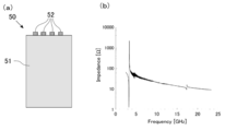
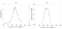
- FIG. 2A shows an Al electrode (wavelength 1.2 ⁇ m, thickness 0.08 wavelength) provided as a blind electrode (IDT) 52 on the surface of a 42 ° YX LT film 51 currently in practical use.
- the frequency characteristics of the SAW resonator 50 shown were determined. The result is shown in FIG. 2 (b).
- the frequency of the basic mode (0th order) was 3.2 GHz
- the band was 3.6%
- the impedance ratio was 65 dB.
- 17.2 GHz a small response that seems to be overtone of 5 times or more is observed, but it can be confirmed that it is not at a usable level.
- the blind electrode 12a is a Cu electrode having a wavelength of 1.2 ⁇ m and a thickness of 0.1 wavelength, and the piezoelectric substrate 11 has an oiler angle (90 °, 90 °, 35 °).
- LT thinness 0.2 wavelength
- the acoustic multilayer film 13 is a low acoustic impedance film 13a (thickness 0.25 wavelength) made of SiO 2 film and a high acoustic impedance film 13b (thickness 0.25 wavelength) made of Ta film.
- Wavelength was alternately laminated in a total of 6 layers, and the frequency characteristics when the support substrate 14 was a Si substrate were determined.
- FIG. 3 (a) The result is shown in FIG. 3 (a).
- the basic mode of SAW was confirmed at 3.8 GHz, and a large response of spurious and its harmonics was confirmed at 2 GHz, 5.1 GHz, 6.3 GHz, and 8.2 GHz.
- an overtone response of about 3 times that of the 0th-order mode was confirmed at 11 GHz.
- the 5.1 GHz response is an LLSAW with a sound velocity of 6,100 m / s.
- Euler angles ( ⁇ , ⁇ , ⁇ ) are simply represented by ( ⁇ , ⁇ , ⁇ ).
- the blind electrode 12a is a Cu electrode having a thickness of 0.1 wavelength
- the piezoelectric substrate 11 is a (90 °, 90 °, 42.5 °) LN (thickness).
- sandwiching the Al electrode of the floating electrode 12b is sandwiching the Al electrode of the floating electrode 12b (thickness 0.01 wavelength)
- the acoustic multilayer film 13 is composed of a SiO 2 film, a low acoustic impedance film 13a (thickness 0.05 wavelength), and Ta.
- the thickness of the Ta film of the high acoustic impedance film 13b is 0.23 from 0.05 wavelength when the high acoustic impedance film 13b made of the film is alternately laminated in a total of 6 layers and the support substrate 14 is a Si substrate. The frequency characteristics when the wavelength was changed were obtained. The result is shown in FIG. 3 (b).
- the characteristic near the center frequency of 3 GHz is the basic mode, and the characteristic near the center frequency is about three times the overtone (“O3” in the figure).
- the characteristic of 12 GHz is about 4 times overtone (“O4” in the figure)
- the characteristic near 15 GHz is about 5 times overtone (“O5” in the figure).
- a characteristic there is one characteristic (hereinafter referred to as A characteristic) between the overtone of about 3 times and the overtone of about 4 times. It was confirmed that when the thickness of the Ta film was 0.115 wavelength, the overtone frequency was reduced by about 3 times and the response was reduced.
- the overtone frequency which was about four times lower, was lowered at the same time, but the response remained small.
- the thickness of the Ta film is 0.13 wavelength
- the frequency of overtone which is about 4 times lower than that when the thickness of Ta film is 0.05 wavelength is further lowered, and the overtone is about 3 times (about 10 GHz), but it is large. It was confirmed that it had an impedance ratio.
- the frequency of each characteristic decreased, and the phenomenon in which the impedance ratio changed to a large or small value was repeated.
- the frequency characteristics of the elastic wave device 10 shown in FIGS. 1A and 1B when various conditions were changed were determined.
- the blind electrode 12a is a Cu electrode having a wavelength of 1.2 ⁇ m and a thickness of 0.1 wavelength
- the piezoelectric substrate 11 is (0 °, 85 °, 0 °) LN.
- the acoustic multilayer film 13 is composed of a low acoustic impedance film 13a (thickness 0.06 wavelength) made of an Al film and a high acoustic impedance film 13b (thickness 0.06 wavelength) made of a W film.
- FIG. 4 (a) shows the frequency characteristics when a total of 6 layers are alternately laminated and the support substrate 14 is a Si substrate.
- the weeping electrode 12a is a Cu electrode 12 having a wavelength of 1.2 ⁇ m and a thickness of 0.1 wavelength
- the piezoelectric substrate 11 is (90 °, 90 °, 42. 5 °) LN (thickness 0.2 wavelength)
- floating electrode 12b as Al electrode
- acoustic multilayer film 13 composed of low acoustic impedance film 13a (thickness 0.05 wavelength) made of SiO 2 film and Ta film.
- FIG. 4B shows the frequency characteristics when the high acoustic impedance film 13b (thickness 0.05 wavelength) is alternately laminated in a total of 6 layers and the support substrate 14 is a Si substrate.
- the blind electrode 12a is a Cu electrode having a wavelength of 1.2 ⁇ m and a thickness of 0.1 wavelength
- the piezoelectric substrate 11 is (0 °, 85 °, 0 °) LT.
- the acoustic multilayer film 13 is composed of a low acoustic impedance film 13a (thickness 0.05 wavelength) made of an Al film and a high acoustic impedance film 13b (thickness 0.05 wavelength) made of a W film.
- 4 (c) shows the frequency characteristics when a total of 6 layers are alternately laminated and the support substrate 14 is a Si substrate. Further, in the elastic wave device 10 shown in FIG.
- the blind electrode 12a is a Cu electrode having a wavelength of 1.2 ⁇ m and a thickness of 0.1 wavelength
- the piezoelectric substrate 11 is (90 °, 90 °, 35 °) LT.
- the floating electrode 12b is an Al electrode
- the acoustic multilayer film 13 is a low acoustic impedance film 13a (thickness 0.07 wavelength) made of a SiO 2 film and a high acoustic impedance film made of a Ta film.
- FIG. 4 (d) shows the frequency characteristics when a total of 6 layers of 13b (thickness 0.07 wavelength) are alternately laminated and the support substrate 14 is a Si substrate.
- the floating electrode 12b shown in FIG. 1A it is preferable that the surface of the Al film in contact with the piezoelectric substrate 11 is an insulating alumite film.
- the magnitude of the SAW basic mode and spurious at 1 to 5 GHz is much smaller than that of the basic mode of FIG. 3 in all frequency characteristics.
- the response of the overtone of 9 to 11 GHz was large, and a band of 3.2 to 8.1% and an impedance ratio of 71 to 76 dB could be obtained.
- the frequency of this overtone corresponds to a sound velocity of 12,000 to 13,000 m / s, which is 3.1 times the frequency of the basic mode shown in FIG.
- the following shows the results when various conditions are changed in order to obtain an overtone with good characteristics.
- the blind electrode 12a is a Cu electrode having a wavelength of 1.2 ⁇ m and a thickness of 0.1 wavelength
- the piezoelectric substrate 11 is a (0 °, ⁇ , 0 °) LN (thickness 0). .2 wavelengths)
- the acoustic multilayer film 13 is alternately composed of a low acoustic impedance film 13a (thickness 0.05 wavelength) made of an Al film and a high acoustic impedance film 13b (thickness 0.05 wavelength) made of a W film.
- the support substrate 14 is a Si substrate (hereinafter, Cu (0.1 ⁇ ) / (0 °, ⁇ , 0 °) LN (0.2 ⁇ ) / Al (0.05 ⁇ )).
- Bandlength when / W (0.05 ⁇ ) / Al (0.05 ⁇ ) / W (0.05 ⁇ ) / Al (0.05 ⁇ ) / W (0.05 ⁇ ) / Si substrate, etc.) The dependence of (Bandwidth) and impedance ratio on the Euler angle ⁇ is shown in FIGS. 5 (a) and 5 (b), respectively.
- the surface of the Al film of the first layer of the acoustic multilayer film 13 on the piezoelectric substrate side may be treated with insulating alumite, or an insulating low acoustic impedance film such as a SiO 2 film may be used. desirable.
- the surface of the Al film of the first layer of the following examples is assumed to be anodized. do.
- the elastic wave device 10 shown in FIG. 1A is Cu (0.1 ⁇ ) / ( ⁇ , 85 °, 0 °) LN (0.2 ⁇ ) / Al (0.05 ⁇ ) / W (0.05 ⁇ ) /.
- the elastic wave device 10 shown in FIG. 1A is Cu (0.1 ⁇ ) / (0 °, 85 °, ⁇ ) LN (0.2 ⁇ ) / Al (0.05 ⁇ ) / W (0.05 ⁇ ) /.
- LN (-30 ° to 30 °, 60 ° to 103 °, -15 ° to 15 °) is used as the piezoelectric substrate 11.
- a band of 3% or more and an impedance ratio of 60 dB or more can be obtained.
- an impedance ratio of 65 dB or more can be obtained, and (-30 ° to 30 °, 78 ° to 92).
- °, -6 ° to 6 °) It can be seen that an impedance ratio of 70 dB or more can be obtained by using LN.
- the elastic wave device 10 shown in FIG. 1A is a Cu (0.1 ⁇ ) / (0 °, 85 °, 0 °) LN (0.2 ⁇ ) / Al film / W film / Al film / W film / Al.
- the dependence of the impedance ratio on the W film thickness when the film thickness of the W film of the high acoustic impedance film 13b is changed with the Al film thickness as 0.05 wavelength is determined. It is shown in FIG. 8 (a).
- FIG. 8B shows the dependence of the impedance ratio on the Al film thickness when the film thickness of the Al film of the low acoustic impedance film 13a is changed with the W film thickness as 0.05 wavelength.
- FIG. 8A shows an example when the Al film thickness is 0.05 wavelength, but even when the Al film thickness is 0.02 to 0.118 wavelength, the optimum W film thickness is the Al film thickness. Showed the same film thickness as when the wavelength was 0.05.
- a large impedance ratio can be obtained even when the Al film thickness of the low acoustic impedance film 13a is 0.2 wavelength or more, and when the Al film thickness is 0.216 to 0.275 wavelength, the impedance is 60 dB or more.
- the ratio is obtained and the Al film thickness is 0.22 to 0.27 wavelength, an impedance ratio of 65 dB or more is obtained, and when the Al film thickness is 0.225 to 0.254 wavelength, an impedance ratio of 70 dB or more is obtained. It was confirmed that it could be obtained.
- FIG. 8B shows an example when the W film thickness is 0.05 wavelength, but even when the W film thickness is 0.02 to 0.118 wavelength, the optimum Al film thickness is the W film thickness. Showed the same film thickness as when the wavelength was 0.05.
- the elastic wave device 10 shown in FIG. 1 (b) is Cu (0.1 ⁇ ) / (0 °, ⁇ , 0 °) LN (0.2 ⁇ ) / floating electrode / Al (0.05 ⁇ ) / W (0. 05 ⁇ ) / Al (0.05 ⁇ ) / W (0.05 ⁇ ) / Al (0.05 ⁇ ) / W (0.05 ⁇ ) / Si
- the dependence of the band and impedance ratio on Euler angles ⁇ for the substrate are shown in FIGS. 9 (a) and 9 (b), respectively.
- the surface of the first Al film of the acoustic multilayer film 13 is anodized with insulation. When an Al electrode that has not been anodized is used in the first layer, the Al film in the first layer may also be used as a floating electrode.
- the elastic wave device 10 shown in FIG. 1 (b) is Cu (0.1 ⁇ ) / (0 °, 85 °, 0 °) LN (0.2 ⁇ ) / floating electrode / Al film / W film / Al film / W.
- the sex is shown in FIG. 10 (a).
- FIG. 10B shows the dependence of the impedance ratio on the Al film thickness when the film thickness of the Al film of the low acoustic impedance film 13a is changed with the W film thickness as 0.05 wavelength.
- a large impedance ratio can be obtained even when the W film thickness of the high acoustic impedance film 13b is 0.2 wavelength or more, and when the W film thickness is 0.216 to 0.275 wavelength, the impedance is 60 dB or more.
- the ratio is obtained and the W film thickness is 0.22 to 0.27 wavelength, an impedance ratio of 65 dB or more is obtained, and when the W film thickness is 0.23 to 0.26 wavelength, an impedance ratio of 70 dB or more is obtained. It was confirmed that it could be obtained.
- FIG. 10A shows an example when the Al film thickness is 0.05 wavelength, but even when the Al film thickness is 0.02 to 0.113 wavelength, the optimum W film thickness is the Al film thickness. Showed the same film thickness as when the wavelength was 0.05.
- a large impedance ratio can be obtained even when the Al film thickness of the low acoustic impedance film 13a is 0.2 wavelength or more, and when the Al film thickness is 0.216 to 0.275 wavelength, the impedance is 60 dB or more.
- the ratio is obtained and the Al film thickness is 0.22 to 0.27 wavelength, an impedance ratio of 65 dB or more is obtained, and when the Al film thickness is 0.225 to 0.254 wavelength, an impedance ratio of 70 dB or more is obtained. It was confirmed that it could be obtained.
- FIG. 10B shows an example when the W film thickness is 0.05 wavelength, but even when the W film thickness is 0.02 to 0.105 wavelength, the optimum Al film thickness is the W film thickness. Showed the same film thickness as when the wavelength was 0.05.
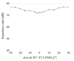
- the elastic wave device 10 shown in FIG. 1A is Cu (0.1 ⁇ ) / (90 °, 90 °, ⁇ ) LN (0.2 ⁇ ) / Al (0.05 ⁇ ) / W (0.05 ⁇ ) /.
- the dependence of the band and impedance ratio on Euler angles ⁇ for Al (0.05 ⁇ ) / W (0.05 ⁇ ) / Al (0.05 ⁇ ) / W (0.05 ⁇ ) / Si substrates is shown in FIG. 11, respectively. It is shown in (a) and (b).
- Euler angles ⁇ and ⁇ are not shown, almost the same values are obtained at ⁇ 6 °, and 60 dB or more at (90 ° ⁇ 6 °, 90 ° ⁇ 6 °, -20 ° to 48 °).
- Impedance ratios of 65 dB or more were obtained at (90 ° ⁇ 6 °, 90 ° ⁇ 6 °, -10 ° to 43 °), and (90 ° ⁇ 6 °, 90 ° ⁇ 6 °,- It was confirmed that an impedance ratio of 70 dB or more can be obtained at (2 ° to 33 °).
- the elastic wave device 10 shown in FIG. 1A is a Cu (0.1 ⁇ ) / (90 °, 90 °, 42.5 °) LN (0.2 ⁇ ) / Al film / W film / Al film / W film.
- FIG. 12 (a) shows the dependence of the impedance ratio on the Al film thickness when the film thickness of the Al film of the low acoustic impedance film 13a is changed with the W film thickness as 0.05 wavelength.
- a large impedance ratio can be obtained even when the W film thickness of the high acoustic impedance film 13b is 0.2 wavelength or more, and when the W film thickness is 0.216 to 0.275 wavelength, the impedance is 60 dB or more.
- the ratio is obtained and the W film thickness is 0.22 to 0.27 wavelength, an impedance ratio of 65 dB or more is obtained, and when the W film thickness is 0.23 to 0.26 wavelength, an impedance ratio of 70 dB or more is obtained. It was confirmed that it could be obtained.
- FIG. 12A shows an example when the Al film thickness is 0.05 wavelength, but even when the Al film thickness is 0.014 to 0.113 wavelength, the optimum W film thickness is the Al film thickness. Showed the same film thickness as when the wavelength was 0.05.
- a large impedance ratio can be obtained even when the Al film thickness of the low acoustic impedance film 13a is 0.2 wavelength or more, and when the Al film thickness is 0.216 to 0.275 wavelength, the impedance is 60 dB or more.
- the ratio is obtained and the Al film thickness is 0.22 to 0.27 wavelength, an impedance ratio of 65 dB or more is obtained, and when the Al film thickness is 0.225 to 0.254 wavelength, an impedance ratio of 70 dB or more is obtained. It was confirmed that it could be obtained.
- FIG. 12B shows an example when the W film thickness is 0.05 wavelength, but even when the W film thickness is 0.015 to 0.104 wavelength, the optimum Al film thickness is the W film thickness. Showed the same film thickness as when the wavelength was 0.05.
- the elastic wave device 10 shown in FIG. 1 (b) is Cu (0.1 ⁇ ) / (90 °, 90 °, ⁇ ) LN (0.2 ⁇ ) / floating electrode / SiO 2 (0.05 ⁇ ) / Ta (0). .05 ⁇ ) / SiO 2 (0.05 ⁇ ) / Ta (0.05 ⁇ ) / SiO 2 (0.05 ⁇ ) / Ta (0.05 ⁇ ) / Si Dependence of band and impedance ratio on Euler angles ⁇
- the sexes are shown in FIGS. 13 (a) and 13 (b), respectively. As shown in FIGS.
- the elastic wave device 10 shown in FIG. 1 (b) is Cu (0.1 ⁇ ) / (90 °, 90 °, 42.5 °) LN (0.2 ⁇ ) / floating electrode / SiO 2 film / Ta film / SiO. 2 film / Ta film / SiO 2 film / Ta film / Si substrate, the impedance ratio when the film thickness of the Ta film of the high acoustic impedance film 13b is changed with the SiO 2 film thickness as 0.05 wavelength.
- FIG. 14 (a) shows the dependence of the impedance ratio on the SiO 2 film thickness when the film thickness of the SiO 2 film of the low acoustic impedance film 13a is changed with the Ta film thickness as 0.05 wavelength. ..
- FIG. 14A shows an example when the SiO 2 film thickness is 0.05 wavelength, but even when the SiO 2 film thickness is 0.012 to 0.096 wavelength, the optimum Ta film thickness is SiO. 2 The film thickness was the same as when the film thickness was 0.05 wavelength.
- the SiO 2 film thickness of the low acoustic impedance film 13a is 0.012 to 0.096 wavelength, 0.12 to 0.185 wavelength, and 0.216 to 0.275 wavelength.
- an impedance ratio of 60 dB or more can be obtained, and at the wavelengths of 0.015 to 0.092 wavelength, 0.125 to 0.18 wavelength, and 0.22 to 0.27 wavelength, an impedance ratio of 65 dB or more can be obtained.
- 0.02 to 0.087 wavelengths, 0.133 to 0.172 wavelengths, and 0.225 to 0.254 wavelengths have an impedance ratio of 70 dB or more, and 0.04 to 0.07 wavelengths have 75 dB. It was confirmed that the above impedance ratio can be obtained.
- FIG. 14B shows an example when the Ta film thickness is 0.05 wavelength, but even when the Ta film thickness is 0.015 to 0.1 wavelength, the optimum SiO 2 film thickness is the Ta film. The film thickness was the same as when the thickness was 0.05 wavelength.
- the elastic wave device 10 shown in FIG. 1A is Cu (0.1 ⁇ ) / (0 °, ⁇ , 0 °) LT (0.15 ⁇ ) / Al (0.05 ⁇ ) / W (0.05 ⁇ ) /.
- the dependence of the band and impedance ratio on Euler angles ⁇ for Al (0.05 ⁇ ) / W (0.05 ⁇ ) / Al (0.05 ⁇ ) / W (0.05 ⁇ ) / Si substrates is shown in FIG. 15, respectively. It is shown in (a) and (b). As shown in FIGS.
- An impedance ratio of 65 dB or more can be obtained with LT ( ⁇ 95 °, -15 ° to 15 °), and an impedance ratio of 70 dB or more can be obtained with LT (-30 ° to 30 °, 70 ° to 89 °, -6 ° to 6 °). Is obtained.
- the elastic wave device 10 shown in FIG. 1A is a Cu (0.1 ⁇ ) / (0 °, 85 °, 0 °) LT (0.15 ⁇ ) / Al film / W film / Al film / W film / Al.
- the dependence of the impedance ratio on the W film thickness when the film thickness of the W film of the high acoustic impedance film 13b is changed with the Al film thickness as 0.05 wavelength is determined. It is shown in FIG. 16 (a).
- FIG. 16B shows the dependence of the impedance ratio on the Al film thickness when the film thickness of the Al film of the low acoustic impedance film 13a is changed with the W film thickness as 0.05 wavelength.
- an impedance ratio of 60 dB or more is obtained and is 0.
- An impedance ratio of 65 dB or more is obtained at .025 to 0.095 wavelength and 0.117 to 0.19 wavelength, and 70 dB or more at 0.03 to 0.092 wavelength and 0.12 to 0.17 wavelength. It was confirmed that the impedance ratio of Although not shown, a large impedance ratio can be obtained even when the W film thickness of the high acoustic impedance film 13b is 0.2 wavelength or more, and when the W film thickness is 0.216 to 0.275 wavelength, the impedance is 60 dB or more.
- FIG. 16A shows an example when the Al film thickness is 0.05 wavelength, the optimum W film thickness is the Al film thickness even when the Al film thickness is 0.02 to 0.1 wavelength. Showed the same film thickness as when the wavelength was 0.05.
- FIG. 16B shows an example when the W film thickness is 0.05 wavelength, the optimum Al film thickness is the W film thickness even when the W film thickness is 0.02 to 0.1 wavelength. Showed the same film thickness as when the wavelength was 0.05.
- the elastic wave device 10 shown in FIG. 1 (b) is Cu (0.1 ⁇ ) / (0 °, ⁇ , 0 °) LT (0.15 ⁇ ) / floating electrode / Al (0.05 ⁇ ) / W (0. 05 ⁇ ) / Al (0.05 ⁇ ) / W (0.05 ⁇ ) / Al (0.05 ⁇ ) / W (0.05 ⁇ ) / Si substrate and Cu (0.1 ⁇ ) / (0 °, ⁇ , 0 °) LT (0.15 ⁇ ) / floating electrode / SiO 2 (0.05 ⁇ ) / Ta (0.05 ⁇ ) / SiO 2 (0.05 ⁇ ) / Ta (0.05 ⁇ ) / SiO 2 (0.05 ⁇ ) ) / Ta (0.05 ⁇ ) / Si substrate, the dependence of the band and the impedance ratio on the oiler angle ⁇ is shown in FIGS.
- the elastic wave device 10 shown in FIG. 1 (b) is Cu (0.1 ⁇ ) / (0 °, 85 °, 0 °) LT (0.15 ⁇ ) / floating electrode / Al film / W film / Al film / W.
- the sex is shown in FIG. 18 (a).
- FIG. 18B shows the dependence of the impedance ratio on the Al film thickness when the film thickness of the Al film of the low acoustic impedance film 13a is changed with the W film thickness as 0.05 wavelength.
- FIG. 18A shows an example when the Al film thickness is 0.05 wavelength, but even when the Al film thickness is 0.023 to 0.098 wavelength, the optimum W film thickness is the Al film thickness. Showed the same film thickness as when the wavelength was 0.05.
- FIG. 18B shows an example when the W film thickness is 0.05 wavelength, but even when the W film thickness is 0.023 to 0.097 wavelength, the optimum Al film thickness is the W film thickness. Showed the same film thickness as when the wavelength was 0.05.
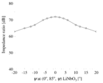
- the elastic wave device 10 shown in FIG. 1A is Cu (0.1 ⁇ ) / (90 °, 90 °, ⁇ ) LT (0.15 ⁇ ) / Al (0.05 ⁇ ) / W (0.05 ⁇ ) /.
- the dependence of the band and impedance ratio on Euler angles ⁇ for Al (0.05 ⁇ ) / W (0.05 ⁇ ) / Al (0.05 ⁇ ) / W (0.05 ⁇ ) / Si substrates is shown in FIG. It is shown in (a) and (b). As shown in FIGS.
- An impedance ratio of 70 dB or more can be obtained at ⁇ 6 °, 90 ° ⁇ 6 °, 85 ° to 91 °), and 75 dB or more at (90 ° ⁇ 6 °, 90 ° ⁇ 6 °, 23 ° to 83 °). It was confirmed that the impedance ratio can be obtained.
- the elastic wave device 10 shown in FIG. 1A is a Cu (0.1 ⁇ ) / (90 °, 90 °, 35 °) LT (0.15 ⁇ ) / Al film / W film / Al film / W film / Al.
- the dependence of the impedance ratio on the W film thickness when the film thickness of the W film of the high acoustic impedance film 13b is changed with the Al film thickness as 0.05 wavelength is determined. It is shown in FIG. 20 (a).
- FIG. 20B shows the dependence of the impedance ratio on the Al film thickness when the film thickness of the Al film of the low acoustic impedance film 13a is changed with the W film thickness as 0.05 wavelength.
- a large impedance ratio can be obtained even when the W film thickness of the high acoustic impedance film 13b is 0.2 wavelength or more, and when the W film thickness is 0.216 to 0.275 wavelength, the impedance is 60 dB or more.
- the ratio is obtained and the W film thickness is 0.22 to 0.27 wavelength, an impedance ratio of 65 dB or more is obtained, and when the W film thickness is 0.225 to 0.26 wavelength, an impedance ratio of 70 dB or more is obtained. It was confirmed that it could be obtained.
- FIG. 20A shows an example when the Al film thickness is 0.05 wavelength, but even when the Al film thickness is 0.018 to 0.08 wavelength, the optimum W film thickness is the Al film thickness. Showed the same film thickness as when the wavelength was 0.05.
- a large impedance ratio can be obtained even when the Al film thickness of the high acoustic impedance film 13b is 0.2 wavelength or more, and when the Al film thickness is 0.216 to 0.275 wavelength, the impedance is 60 dB or more.
- the ratio is obtained and the Al film thickness is 0.22 to 0.27 wavelength, an impedance ratio of 65 dB or more is obtained, and when the Al film thickness is 0.225 to 0.26 wavelength, an impedance ratio of 70 dB or more is obtained. It was confirmed that it could be obtained.
- FIG. 20B shows an example when the W film thickness is 0.05 wavelength, but even when the W film thickness is 0.016 to 0.08 wavelength, the optimum Al film thickness is the W film thickness. Showed the same film thickness as when the wavelength was 0.05.
- the elastic wave device 10 shown in FIG. 1 (b) is Cu (0.1 ⁇ ) / (90 °, 90 °, ⁇ ) LT (0.15 ⁇ ) / floating electrode / SiO 2 (0.05 ⁇ ) / Ta (0). .05 ⁇ ) / SiO 2 (0.05 ⁇ ) / Ta (0.05 ⁇ ) / SiO 2 (0.05 ⁇ ) / Ta (0.05 ⁇ ) / Si Dependence of band and impedance ratio on Euler angles ⁇
- the sexes are shown in FIGS. 21 (a) and 21 (b), respectively. As shown in FIGS.
- the elastic wave device 10 shown in FIG. 1B is a Cu (0.1 ⁇ ) / (90 °, 90 °, 35 °) LT (0.15 ⁇ ) / floating electrode / SiO 2 film / Ta film / SiO 2 film. / Ta film / SiO 2 film / Ta film / Si substrate, Ta film of impedance ratio when the film thickness of Ta film of high acoustic impedance film 13b is changed with SiO 2 film thickness as 0.05 wavelength.
- the dependence on the film thickness is shown in FIG. 22 (a). Further, FIG. 22B shows the dependence of the impedance ratio on the SiO 2 film thickness when the film thickness of the SiO 2 film of the low acoustic impedance film 13a is changed with the Ta film thickness as 0.05 wavelength. ..
- FIG. 22A shows an example when the SiO 2 film thickness is 0.05 wavelength, but even when the SiO 2 film thickness is 0.015 to 0.085 wavelength, the optimum Ta film thickness is SiO. 2 The film thickness was the same as when the film thickness was 0.05 wavelength.
- the SiO 2 film thickness of the low acoustic impedance film 13a is 0.015 to 0.085 wavelength, 0.118 to 0.18 wavelength, and 0.216 to 0.275 wavelength.
- an impedance ratio of 60 dB or more is obtained, and at 0.017 to 0.093 wavelength, 0.122 to 0.175 wavelength, and 0.22 to 0.27 wavelength, an impedance ratio of 65 dB or more is obtained.
- 0.02 to 0.087 wavelength, 0.13 to 0.17 wavelength, and 0.225 to 0.26 wavelength an impedance ratio of 70 dB or more is obtained, and 0.035 to 0.08 wavelength. It was confirmed that an impedance ratio of 75 dB or more could be obtained.
- FIG. 20B shows an example when the Ta film thickness is 0.05 wavelength, but even when the Ta film thickness is 0.015 to 0.085 wavelength, the optimum SiO 2 film thickness is the Ta film. The film thickness was the same as when the thickness was 0.05 wavelength.
- the elastic wave device 10 shown in FIG. 1 (b) is Cu (0.1 ⁇ ) / (90 °, 90 °, 42.5 °) LN (0.2 ⁇ ) / floating electrode / SiO 2 film (0.05 ⁇ ).
- FIG. 23 shows the dependence of the impedance ratio on the thickness of the piezoelectric substrate 11 in the case of 05 ⁇ ) / Ta film (0.05 ⁇ ) / SiO 2 film (0.05 ⁇ ) / Ta film (0.05 ⁇ ) / Si substrate. Shown in. As shown in FIG. 23, when the thicknesses of LN and LT are 5 wavelengths or less and 2.4 wavelengths or less, an impedance ratio of 65 dB or more is obtained, and the thicknesses of LN and LT are 1.2 wavelengths or less and 1 wavelength, respectively.
- an impedance ratio of 70 dB or more can be obtained, and when the thicknesses of LN and LT are 0.3 to 0.02 wavelength and 0.25 to 0.02 wavelength, respectively, an impedance ratio of 75 dB or more can be obtained. confirmed.
- the elastic wave device 10 shown in FIG. 1 (b) is Cu (0.1 ⁇ ) / (90 °, 90 °, 35 °) LT (0.15 ⁇ ) / floating electrode / SiO 2 film (0.05 ⁇ ) / Ta.
- the dependence of the acoustic multilayer film 13 on the number of layers is shown in FIG. As shown in FIG.
- the film such as Ti provided to increase the adhesive strength has a film thickness of several tens of nm to several hundreds of nm, and the acoustic multilayer film 13 has a thickness of several tens of nm to several hundreds of nm. Since it is relatively thin compared to each film, it is not included as an acoustic impedance film.
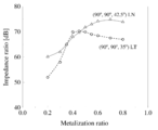
- the elastic wave device 10 shown in FIG. 1B is a blind electrode 12a / (90 °, 90 °, 35 °) LT (0.15 ⁇ ) / floating electrode / SiO 2 film (0.05 ⁇ ) / Ta film ( 0.05 ⁇ ) / SiO 2 film (0.05 ⁇ ) / Ta film (0.05 ⁇ ) / SiO 2 film (0.05 ⁇ ) / Ta film (0.05 ⁇ ) / Si substrate (0.05 ⁇ ) / Si substrate
- FIG. 25 the metallization ratio (MR) of the blind electrode 12a is set to 0.5, and the results when a Cu electrode, an Al electrode, an Au electrode, and a Mo electrode are used as the blind electrode 12a are shown.
- the electrode thickness when the electrode thickness is 0.01 to 0.045 wavelength and 0.1 to 0.21 wavelength, an impedance ratio of 65 dB or more can be obtained, and the electrode thickness is 0.02 to 0.041 wavelength and It was confirmed that an impedance ratio of 70 dB or more was obtained when the wavelength was 0.135 to 0.197, and an impedance ratio of 75 dB or more was obtained when the electrode thickness was 0.159 to 0.182 wavelength.
- the electrode thickness is 0.005 to 0.02 wavelength and 0.062 to 0.165 wavelength
- an impedance ratio of 65 dB or more can be obtained, and the electrode thickness is 0.01 to 0.0152 wavelength and It was confirmed that an impedance ratio of 70 dB or more was obtained when the wavelength was 0.064 to 0.155, and an impedance ratio of 75 dB or more was obtained when the electrode thickness was 0.08 to 0.12 wavelength.
- the electrode thickness when the electrode thickness is 0.008 to 0.03 wavelength and 0.055 to 0.19 wavelength, an impedance ratio of 65 dB or more can be obtained, and the electrode thickness is 0.0125 to 0.027 wavelength and It was confirmed that an impedance ratio of 70 dB or more was obtained when the wavelength was 0.065 to 0.165, and an impedance ratio of 75 dB or more was obtained when the electrode thickness was 0.095 to 0.13 wavelength.
- interdigital electrodes 12a when the density is less than 1800 kg / m 3 or more 6000 kg / m 3, the same electrode thickness and the Al electrode becomes optimum thickness, when less than 6000 kg / m 3 or more 10000 kg / m 3, and the Cu electrode
- the same electrode thickness is the optimum thickness, and when it is 10000 kg / m 3 or more and less than 15000 kg / m 3 , the same electrode thickness as the Mo electrode is the optimum thickness, and when it is 15000 kg / m 3 or more and less than 25000 kg / m 3 , the same electrode as the Au electrode.
- the thickness is the optimum thickness.
- the optimum thickness is determined by converting with the average density thereof.
- the metallization ratio (MR) of the blind electrode 12a deviates from 0.5
- the optimum thickness is H ⁇ 0.5 / MR, where H is the optimum thickness when the MR is 0.5.
- the elastic wave device 10 shown in FIG. 1 (b) is Cu (0.1 ⁇ ) / (90 °, 90 °, 42.5 °) LN (0.2 ⁇ ) / floating electrode / SiO 2 film (0.05 ⁇ ).
- FIG. 26 The dependence of the impedance ratio on the MR of the weeping electrode 12a in the case of 05 ⁇ ) / Ta film (0.05 ⁇ ) / SiO 2 film (0.05 ⁇ ) / Ta film (0.05 ⁇ ) / Si substrate is shown in FIG. 26. Shown in. As shown in FIG. 26, it was confirmed that an impedance ratio of 65 dB or more can be obtained when the MR is 0.35 to 0.8 for both LN and LT. Further, it was confirmed that in LN, an impedance ratio of 70 dB or more was obtained when MR was 045 to 0.8, and in LT, an impedance ratio of 68 dB or more was obtained when MR was 0.45 to 0.6. Was done.
- the elastic wave device 10 shown in FIG. 1A is a Cu (0.1 ⁇ ) / (90 °, 90 °, 42.5 °) LN (0.2 ⁇ ) / acoustic multilayer film [Multi acoustic layers; SiO]. 2 (0.05 ⁇ ) / Ta (0.05 ⁇ ) / SiO 2 (0.05 ⁇ ) / Ta (0.05 ⁇ ) / SiO 2 (0.05 ⁇ ) / Ta (0.05 ⁇ ) / SiO 2 (0.05 ⁇ ) ) / Ta (0.05 ⁇ )] / Si substrate, the displacement distribution of the frequency characteristic of the overtone near the sound velocity of 11,000 m / s is shown in FIG. 27 (b). As shown in FIG.
- the mutation distribution was SAW containing the SH component as a main component.
- the elastic wave device of Patent Document 3 and the elastic wave device 10 of the embodiment of the present invention have a completely different displacement distribution in addition to the difference in frequency and sound velocity, the difference in the basic mode of LLSAW and the overtone of SAW. From the different, it is clear that the vibration modes are also different.
Landscapes
- Physics & Mathematics (AREA)
- Acoustics & Sound (AREA)
- Chemical & Material Sciences (AREA)
- Engineering & Computer Science (AREA)
- Materials Engineering (AREA)
- Surface Acoustic Wave Elements And Circuit Networks Thereof (AREA)
Abstract
【課題】オーバートーンを用いて、6GHz以上の超高周波数帯で、良好な特性を得ることができる弾性波デバイスを提供する。 【解決手段】圧電基板11と、圧電基板11に接するよう設けられた電極12と、圧電基板11および/または電極12に接するよう設けられた音響多層膜13とを有し、弾性表面波の共振特性のうちのオーバートーンを利用するよう構成されている。電極12は、圧電基板11の一方の表面に設けられたすだれ状電極12aを有している。オーバートーンの弾性表面波は、音速9000m/s以上であることが好ましい。音響多層膜13は、低音響インピーダンス膜13aと高音響インピーダンス膜13bとが交互に積層されていることが好ましい。
Description
本発明は、弾性波デバイスに関する。
スマートフォン等で主に使用されている700MHzから3GHzの周波数帯には、80近くのバンドがあり、非常に混雑している。その対策として、第5世代移動通信システム(5G)では、3.3GHzから4.9GHzの周波数帯が使用されつつあり、また、その次の世代では、6GHz以上の周波数帯を使用する計画がなされている。
従来、700MHzから3GHzの周波数帯では、AlNやScAlNの圧電薄膜を用いたバルク弾性波(FBAR;Film Bulk Acoustic Resonator)デバイス(例えば、非特許文献1または2参照)や、圧電基板や薄膜としてLiNbO3結晶(LN)やLiTaO3結晶(LT)を用いた弾性表面波(SAW)デバイスや縦波漏洩弾性波(LLSAW)を用いたデバイスが用いられている(例えば、非特許文献3または4参照)。弾性表面波(SAW)デバイスでは、帯域が、用いる圧電基板の電気機械結合係数(結合係数)に依存するため、その帯域に必要な結合係数を有するLNやLT基板が一般的に使用されている。
このうち、FBARデバイスでは、AlNやScAlN膜などがc軸配向しているため、用いるバルク波の振動モードは、厚み縦振動のみとなる。この縦波の音速は、(c33D/密度)1/2で表され(c33Dは弾性スティッフネス定数)、励振周波数は、音速/(2×膜厚)で表される値に、電極の質量負荷による周波数低下分を減じた周波数になる。このため、励振周波数を高周波にするためには、圧電薄膜の膜厚を極端に薄くしなければならない。しかし、圧電薄膜としてAlNやScAlNを用いたものは、これらが多結晶薄膜であるため、超高周波での減衰が大きく、良好な特性を実現するのが困難であった。
また、圧電基板としてLNやLTを用いた弾性表面波(SAW)デバイスでは、周波数fは、基板の音速Vと、すだれ状電極の周期(波長λ)とから、f=V/λで決まる。耐電力や製造課程でのバラツキの関係から、すだれ状電極の波長は、1.2μm程度が限界であるため、用いる基板の音速との関係から、高周波側では約3.2GHzの周波数が限界であった。
なお、サファイアのような高音速の基板上にZnOのような圧電膜を形成した時、圧電膜の厚みに応じて、基本モードのレイリー波(0次)と、その高次モードのセザワ波(1次)やさらにその高次モード(2次、3次、・・・)の波が励振されるが、その高次モードの周波数は、基本モードの周波数の整数倍ではない。一方、バルク波の厚み振動では、基本モードの他に、約2倍、3倍・・・の整数倍の周波数(Harmonic周波数)を有するオーバートーンが励振される。このように、基本モードの約2倍、3倍・・と励振されるSAWを、以下でも、オーバートーンと呼ぶ。
また、後述の板波のうち、非対称ラム波の0次モード(A0モード)は基板厚が薄くなるにつれて音速が遅くなるが、その高次の1次モードのA1モードは逆に速くなり、その比は圧電基板の厚みにより大きく異なる。その上、両者は整数倍の関係にはない。上述のセザワ波のように、A1モードは、A0モードの高次モードであって、オーバートーンではない。
上述のように、SAWデバイスでは、高周波側で約3.2GHzが限界であるが、SAW以外では、板波を用いた3.2GHz以上の高周波デバイスの報告がある。板波には、縦波成分と、shear vertical(SV)成分の変位を有するA0モードやA1モードやS0モードのラム波と、shear horizontal(SH)成分を有するSH0モードのSH型板波とがある。これらの板波は、基板内全体が振動して伝わり、基板表面に集中して伝搬するSAWとは大きく異なり、板波とSAWとは区別して利用されている。
圧電基板の厚みが波長の0.15倍以下のとき、S0モードでは、SAWの約1.5倍の6,000m/sの高音速が得られ、A1モードでは、約3~6倍の12,000~25,000m/sの高音速が得られ、高周波化デバイスの実現には有利である。そこで、0.34~0.48μmのLNやLT薄膜中のA1モードの基本波を用い、4.5~6.3GHzの共振子デバイスが実現されている(例えば、非特許文献5または6参照)。しかし、このデバイスは、板波を励振する圧電薄板上のIDT部の上下部ともに空洞を必要とするため、0.48μm以下の薄板では、機械的強度が弱いという大きな課題がある。
そこで、この板波の機械的強度が弱いという問題を解決するために、圧電薄板に接するように音響多層膜を用いることにより、圧電薄板の下部に空洞を必要としない構造を有し、A1モード、S0モード、SH0モードの板波の基本モードを励振するもの(例えば、非特許文献7または特許文献1参照)や、SH0モード板波の基本モードを用いたもの(例えば、特許文献2参照)が提案されている。また、LNやLTを用い、LLSAWの基本モードを用いたものも提案されている(例えば、特許文献3参照)。
John D. Larson III et al., "Power Handling and Temperature Coefficient Studies in FBAR Duplexers for the 1900 MHz PCS Band", Proc. IEEE Ultrason. Symp., 2000, p.869-874
Keiichi Umeda et al., "PIEZOELECTRIC PROPERTIES OF ScAlN THIN FILMS FOR PIRZO-MEMS DEVICES", Proc. MEMS (Taipei, Taiwan), 2013, p.20-24,
M. Kadota, Y. Ishii, T. Shimatsu, M. Umoto, and Shuji Tanaka, "Suprious-Free, Near-Zero-TCF Hetero Acoustic Layer (HAL) SAW Resonators Using LiTaO3 Thin Plate on Quartz", Proc. IEEE Ultrason. Symp., 2018, 6J-2
T. Kimura, Y. Kishimoto, M. Omura and K. Hashimoto, "3.5 GHz longitudinal leaky surface acoustic wave resonator using a multilayered waveguide structure for high acoustic energy confinement", Jpn. J. Appl. Phys., 2018, vol. 57, 07LD15
M. Kadota, T. Ogami, K. Yamamoto, H. Tochishita, and Y. Negoro, "High frequency Lamb Wave Device composed of MEMS Structure using LiNbO3 Thin Film and Air Gap", IEEE trans. Ultrason. Ferroelec. Freq. Cont., 2010, vol.57, No.11, p.2564-2571
N. Assila, M. Kadota, and S. Tanaka, "High Frequency Resonator Using A1 Mode Lamb Wave in LiTaO3 Plate", IEEE trans. Ultrason. Ferroelec. Freq. Cont., 2019, vol. 66, No. 9, p. 1529-1535
T. Kimura, K. Daimon, T. Ogami and M. Kadota, "S0 Mode Lamb Wave Resonators Using Thin Plate LiNbO3 and Acoustic Quarter-Wave Multilayers", Jpn. J. Appl. Phys., 2013, vol. 52, 07HD03
清水康敬,「LiTaO3基板弾性表面波伝搬の方位特性」、音響学会誌、1980年、vol.36、p.140-145
非特許文献1および2に記載のようなFBARデバイスでは、6GHz以上の超高周波数帯で、インピーダンス比が大きい良好な特性を得ることはできないという課題があった。また、非特許文献3または4に記載のように、従来の弾性表面波(SAW)や縦波漏洩弾性波(LLSAW)を用いたデバイスは、圧電薄膜の上にすだれ状電極(IDT)を形成した構造では、基本モードしか励振せず、圧電薄膜と支持基板、あるいは音響多層膜と支持基板とを組み合わせた構造であっても、基本モードの整数倍の周波数を有するオーバートーンは励振されず、高周波側の周波数は、共振周波数で3.5GHzが限界であるという課題があった。
特許文献1に記載のデバイスでは、A1モード板波は、基本モードの反共振周波数で決定される音速は15,500m/sを有しているが、その音速は、A1モード板波の基本モードの音速であり、オーバートーンの音速ではないという課題があった。また、非特許文献5、6、7に記載のデバイスでは、方位角、基板厚に関わらず、LiNbO3(LN)やLiTaO3(LT)のS0モードの音速が、6,000~7,000m/sとなっているが、これもオーバートーンを用いたものではないという課題があった。なお、特許文献1および2に記載のSH0モード板波デバイスについては、その音速が記されていないが、非特許文献5、6、7に記載のデバイスでは、方位角、基板厚に関わらず、LNやLTのSH0モード板波の音速は約4,000m/sとなっている。
特許文献3の記載のデバイスでは、0.05、0.06、0.08波長厚のAl電極を用い、LLSAWを励振しているが、そのAlの電極厚みでは、オーバートーンを大きく励振することはできないという課題があった。なお、特許文献3の記載のデバイスでは、LLSAWの基本モードの音速は約6,000m/sとなっている。
本発明は、このような課題に着目してなされたもので、オーバートーンを用いて、6GHz以上の超高周波数帯で、良好な特性を得ることができる弾性波デバイスを提供することを目的とする。
上記目的を達成するために、本発明に係る弾性波デバイスは、圧電基板と、前記圧電基板に接するよう設けられた電極と、前記圧電基板および/または前記電極に接するよう設けられた音響多層膜とを有し、弾性表面波の共振特性のうちのオーバートーンを利用するよう構成されていることを特徴とする。
本発明に係る弾性波デバイスは、音響多層膜により、弾性表面波の基本モードの周波数の約整数倍(約2倍、約3倍、・・・)のオーバートーンを励振することができる。また、電極の厚みや、圧電基板の種類、音響多層膜の各層の厚みを調整することにより、大きいインピーダンス比を有する弾性表面波のオーバートーンを得ることができる。本発明に係る弾性波デバイスは、このオーバートーンを利用することにより、6GHz以上の超高周波数帯で、インピーダンス比が大きい良好な特性を得ることができる。このオーバートーンの弾性表面波は、例えば、音速が9000m/s以上に相当し、場合によっては、10000m/s以上に相当する。
なお、ここで、弾性波デバイスのインピーダンス比(Impedance ratio)は、共振周波数frにおける共振インピーダンスZrと、反共振周波数faにおける反共振インピーダンスZaとの比[20×log(Za/Zr)]である。また、弾性波デバイスの帯域(Bandwidth)は、(fa-fr)/frである。
本発明に係る弾性波デバイスで、前記音響多層膜は、低音響インピーダンス膜と高音響インピーダンス膜とが交互に積層されていることが好ましい。特に、前記音響多層膜は、低音響インピーダンス膜と高音響インピーダンス膜とが交互に連続して3層以上20層以下で積層された音響膜を有することが好ましい。また、この場合、前記音響多層膜の各低音響インピーダンス膜および各高音響インピーダンス膜のうち、少なくとも3層の各厚みが、それぞれ前記弾性表面波の0.012波長~0.118波長、0.105波長~0.2波長、または、0.216波長~0.275波長であることが好ましい。また、0.015波長~0.117波長、0.105波長~0.19波長、または、0.22波長~0.27波長であることがより好ましい。また、0.02波長~0.12波長、0.114波長~0.172波長、または、0.225波長~0.26波長であることがさらに好ましい。また、0.03波長~0.082波長であることがさらに好ましい。さらに、前記音響多層膜の低音響インピーダンス膜および高音響インピーダンス膜の組み合わせの内、いずれか片方の膜の厚みは、0.012波長~0.118波長、あるいは0.02波長~0.12波長、あるいは0.03波長~0.082波長であることがより好ましい。これにより、弾性表面波のオーバートーンを効率よく励振することができる。
本発明に係る弾性波デバイスで、前記音響多層膜の各低音響インピーダンス膜および/または各高音響インピーダンス膜は、Mg合金、SiO2、SiOF、Al、Y、Si、Ge、Ti、ZnO、SixNy(ここで、xおよびyは正の実数)、AlN、SiC、Al2O3、Ag、ZrO2、Hf、Cu、TiO2、Cr、Ni、Au、Ta、Mo、Pt、およびWのうちの少なくとも1つを含む膜、または、これらのうちの少なくとも1つを含む酸化膜、窒化膜、炭化膜もしくはヨウ化膜から成ることが好ましい。それ以外でも、低音響インピーダンス膜は、隣り合う高音響インピーダンス膜よりも、音響インピーダンスが小さいものから成っていればよい。なお、本発明に係る弾性波デバイスで、各低音響インピーダンス膜および各高音響インピーダンス膜の、縦波での音響インピーダンスZlおよび横波での音響インピーダンスZsは、それぞれ(密度×c33)1/2および(密度×c44)1/2で表される(c33、c44は弾性スティッフネス定数である)。用いる2つの音響膜のうち、Z1の小さい方またはZsの小さい方が低音響インピーダンス膜であり、大きい方が高音響インピーダンス膜である。
本発明に係る弾性波デバイスで、前記圧電基板は、LiNbO3またはLiTaO3の単結晶から成ることが好ましい。この場合、弾性表面波のオーバートーンを励振しやすい。
本発明に係る弾性波デバイスは、大きいインピーダンス比を得るために、前記電極は、前記圧電基板の一方の表面に設けられたすだれ状電極から成り、前記音響多層膜は、前記圧電基板の他方の表面に接するよう設けられ、前記圧電基板は、LiNbO3結晶から成り、オイラー角が(-30°~30°,60°~103°,-15°~15°)および(90°±6°,90°±6°,-20°~48°)のいずれか一方、または、これらのいずれか一方と結晶学的に等価なオイラー角であることが好ましい。また、この場合、圧電基板は、オイラー角が(-30°~30°,72°~97°,-15°~15°)および(90°±6°,90°±6°,-10°~43°)のいずれか一方、または、これらのいずれか一方と結晶学的に等価なオイラー角であることがより好ましい。また、この場合、圧電基板は、オイラー角が(-30°~30°,78°~92°,-6°~6°)および(90°±6°,90°±6°,-2°~33°)のいずれか一方、または、これらのいずれか一方と結晶学的に等価なオイラー角であることがさらに好ましい。
本発明に係る弾性波デバイスは、大きいインピーダンス比を得るために、前記電極は、前記圧電基板の一方の表面に設けられたすだれ状電極と、前記圧電基板の他方の表面を覆うよう設けられた浮き電極とを有し、前記音響多層膜は、前記浮き電極の前記圧電基板とは反対側の表面に接するよう設けられ、前記圧電基板は、LiNbO3結晶から成り、オイラー角が(-30°~30°,64°~98°,-15°~15°)および(90°±6°,90°±6°,-4°~56°)のいずれか一方、または、これらのいずれか一方と結晶学的に等価なオイラー角であることが好ましい。また、この場合、圧電基板は、オイラー角が(-30°~30°,68°~95°,-15°~15°)および(90°±6°,90°±6°,-2°~52°)のいずれか一方、または、これらのいずれか一方と結晶学的に等価なオイラー角であることがより好ましい。また、この場合、圧電基板は、オイラー角が(-30°~30°,72°~92°,-15°~15°)および(90°±6°,90°±6°,25°~50°)のいずれか一方、または、これらのいずれか一方と結晶学的に等価なオイラー角であることがさらに好ましい。なお、浮き電極は、すだれ状電極の片方の電極、または、本発明に係る弾性波デバイス以外の他の共通電極と接続されていてもよい。
この圧電基板がLiNbO3結晶から成る場合、圧電基板の厚みが前記弾性表面波の0.002~5波長であることが好ましく、1.2波長以下であることがより好ましく、0.02~0.3波長であることがさらに好ましい。この場合、より大きいインピーダンス比を得ることができる。
本発明に係る弾性波デバイスは、大きいインピーダンス比を得るために、前記電極は、前記圧電基板の一方の表面に設けられたすだれ状電極から成り、前記音響多層膜は、前記圧電基板の他方の表面に接するよう設けられ、前記圧電基板は、LiTaO3結晶から成り、オイラー角が(-30°~30°,55°~100°,-15°~15°)、(90°±6°,90°±6°,-5°~61°)および(90°±6°,90°±6°,83°~93°)のいずれか一つ、または、これらのいずれか一つと結晶学的に等価なオイラー角であることが好ましい。また、この場合、圧電基板は、オイラー角が(-30°~30°,61°~95°,-15°~15°)、(90°±6°,90°±6°,15°~55°)および(90°±6°,90°±6°,85°~91°)のいずれか一つ、または、これらのいずれか一つと結晶学的に等価なオイラー角であることがより好ましい。また、この場合、圧電基板は、オイラー角が(-30°~30°,70°~89°,-15°~15°)および(90°±6°,90°±6°,23°~38°)のいずれか一方、または、これらのいずれか一方と結晶学的に等価なオイラー角であることがより好ましい。
本発明に係る弾性波デバイスは、大きいインピーダンス比を得るために、前記電極は、前記圧電基板の一方の表面に設けられたすだれ状電極と、前記圧電基板の他方の表面を覆うよう設けられた浮き電極とを有し、前記音響多層膜は、前記浮き電極の前記圧電基板とは反対側の表面に接するよう設けられ、前記圧電基板は、LiTaO3結晶から成り、オイラー角が(-30°~30°,65°~94°,-15°~15°)および(90°±6°,90°±6°,-4°~56°)のいずれか一方、または、これらのいずれか一方と結晶学的に等価なオイラー角であることが好ましい。また、この場合、圧電基板は、オイラー角が(-30°~30°,69°~91°,-15°~15°)および(90°±6°,90°±6°,-2°~52°)のいずれか一方、または、これらのいずれか一方と結晶学的に等価なオイラー角であることがより好ましい。また、この場合、圧電基板は、オイラー角が(90°±6°,90°±6°,25°~50°)、または、これと結晶学的に等価なオイラー角であることがさらに好ましい。なお、浮き電極は、すだれ状電極の片方の電極、または、本発明に係る弾性波デバイス以外の他の共通電極と接続されていてもよい。
圧電基板がLiTaO3結晶から成る場合、圧電基板の厚みが前記弾性表面波の0.002~2.4波長であることが好ましく、1波長以下であることがより好ましく、0.02~0.25波長であることがさらに好ましい。この場合、より大きいインピーダンス比を得ることができる。
本発明に係る弾性波デバイスで、前記すだれ状電極は、メタライジェイション比をMRとし、前記弾性表面波の波長をλとすると、密度が1800kg/m3以上6000kg/m3未満で、厚みが(0.01λ~0.045λ)×0.5/MRもしくは(0.1λ~0.21λ)×0.5/MR、または、密度が6000kg/m3以上10000kg/m3未満で、厚みが(0.01λ~0.033λ)×0.5/MRもしくは(0.06λ~0.2λ)×0.5/MR、または、密度が10000kg/m3以上15000kg/m3未満で、厚みが(0.008λ~0.03λ)×0.5/MRもしくは(0.055λ~0.19λ)×0.5/MR、または、密度が15000kg/m3以上25000kg/m3未満で、厚みが(0.005λ~0.02λ)×0.5/MRもしくは(0.062λ~0.165λ)×0.5/MRであることが好ましい。この場合、より大きいインピーダンス比を得ることができる。なお、すだれ状電極(IDT)のメタライゼーション比(MR)は、弾性表面波の伝搬方向に沿って、すだれ状電極の電極指の幅Fを、電極指の周期(λ)の半分(電極指の幅Fと電極指間の隙間Gとの和)で除した比率であり、MR=F/(F+G)=2×F/λである。また、すだれ状電極の電極指の周期(波長)λが、利用する弾性表面波の波長と等しくなる。
ここで、オイラー角(φ、θ、ψ)は、右手系であり、圧電基板の切断面と、弾性波の伝搬方向とを表現するものである。すなわち、圧電基板を構成する結晶や、LTまたはLNの結晶軸X、Y、Zに対し、Z軸を回転軸としてX軸を反時計廻りにφ回転し、X’軸を得る。次に、そのX’軸を回転軸としてZ軸を反時計廻りにθ回転しZ’軸を得る。このとき、Z’軸を法線とし、X’軸を含む面を、圧電基板の切断面とする。また、Z’軸を回転軸としてX’軸を反時計廻りにψ回転した方向を、弾性波の伝搬方向とする。また、これらの回転によりY軸が移動して得られる、X’軸およびZ’軸と垂直な軸を、Y′軸とする。
オイラー角をこのように定義することにより、非特許文献8によれば、三方晶系3m点群に属するLN、LTでは次の関係が成り立つ。
(φ、θ、ψ)=(60°+φ、-θ、ψ)=(60°-φ、-θ、180°-ψ)
=(φ、180°+θ、180°-ψ)=(φ、θ、180°+ψ)
例えば、40°回転Y板X方向伝搬は、オイラー角で(0°、130°、0°)と表され、40°回転Y板90°X方向伝搬は、オイラー角で(0°、130°、90°)と表される。なお、圧電基板を所望のオイラー角で切り出す際には、オイラー角の各成分に対して、最大で±0.5°程度の誤差が発生する可能性がある。弾性波の特性に関しては、(φ、θ、ψ)のオイラー角のうち、φ、ψに関しては、±5°程度のずれによる特性差はほとんどない。また、オイラー角(0°、θ、0°)に対し、(0°、θ+360°、0°)は、オイラー角で等価な面である。一方、(0°、θ+180°、0°)は、(0°、θ、0°)とはオイラー角で等価な面ではないが、基板の表裏の関係にある。しかし、弾性波デバイスでは、表と裏でも同じ特性を示すため、ここでは、基板の表裏の関係の方位も、等価な面とみなす。
本発明によれば、オーバートーンを用いて、6GHz以上の超高周波数帯で、良好な特性を得ることができる弾性波デバイスを提供することができる。
以下、図面および実施例に基づいて、本発明の実施の形態について説明する。
図1乃至図27は、本発明の実施の形態の弾性波デバイスを示している。
図1に示すように、弾性波デバイス10は、弾性表面波の共振特性のうちのオーバートーンを利用するよう構成されており、圧電基板11と電極12と音響多層膜13と支持基板14とを有している。
図1乃至図27は、本発明の実施の形態の弾性波デバイスを示している。
図1に示すように、弾性波デバイス10は、弾性表面波の共振特性のうちのオーバートーンを利用するよう構成されており、圧電基板11と電極12と音響多層膜13と支持基板14とを有している。
図1(a)に示すように、圧電基板11は、LiNbO3の単結晶(LN)またはLiTaO3の単結晶(LT)から成っている。電極12は、すだれ状電極(IDT)12aから成り、圧電基板11の一方の表面にフォトリソグラフィー工程等により形成されている。すだれ状電極12aは、電極指の周期(波長)λが、利用する基本モードおよびオーバートーンの弾性表面波の波長と等しくなっている。なお、以下では、波長(λ)は、電極指の周期(波長)、すなわち利用する基本モードおよびオーバートーンの弾性表面波の波長を表している。
音響多層膜13は、圧電基板11のIDTとは反対側の表面に貼り付けられている。音響多層膜13は、圧電基板11の側からその反対側に向かって、低音響インピーダンス膜13aと高音響インピーダンス膜13bとが交互に積層されている。また、音響多層膜13は、低音響インピーダンス膜13aと高音響インピーダンス膜13bとが交互に連続して3層以上20層以下で積層された音響膜を有することが好ましい。図1(a)に示す具体的な一例では、最も圧電基板11に近い層が低音響インピーダンス膜13aであり、低音響インピーダンス膜13aと高音響インピーダンス膜13bとが交互に連続して6層積層されている。
各低音響インピーダンス膜13aおよび各高音響インピーダンス膜13bは、表1または表2に示す材料の少なくとも1つを含む膜から成っている。なお、表1中のZlは、弾性表面波の縦波の音響インピーダンス、c33は弾性スティッフネス定数、表2中のZsは、弾性表面波の横波の音響インピーダンス、c44は弾性スティッフネス定数である。また、表1中および表2中のSixNyの、xおよびyは正の実数である。また、表1のZl、表2のZsのどちらの音響インピーダンスが寄与するかは、SAWの変位による。すなわち、縦波成分の多いSAWではZlに、SH成分が多いSAWではZsに依存する。


各低音響インピーダンス膜13aは、隣り合う高音響インピーダンス膜13bよりも、音響インピーダンスが小さいものから成っている。各低音響インピーダンス膜13aは、同じものから成っていてもよいが、異なるものから成っていてもよい。また、各高音響インピーダンス膜13bも、同じものから成っていてもよいが、異なるものから成っていてもよい。
支持基板14は、圧電基板11との間に音響多層膜13を挟むよう、音響多層膜13の圧電基板11とは反対側の面に貼り付けられている。支持基板14は、圧電基板11や電極12、音響多層膜13を支持するよう設けられている。図1(a)に示す具体的な一例では、支持基板14は、Si基板から成っているが、その他にも、ガラス基板や水晶基板、アルミナ基板、サファイア基板、ゲルマニウム基板などから成っていてもよい。なお、図1(a)では、音響多層膜と反対側の圧電基板の表面にIDTが設けられているが、IDTは、圧電基板と音響多層膜との間に設けられていてもよい。
なお、図1(b)に示すように、弾性波デバイス10は、圧電基板11と音響多層膜13との間に設けられた浮き電極(短絡電極と呼ばれることもある)12bを有していてもよい。浮き電極12bは、すだれ状電極12aと同じ材料から成っていてもよく、異なる材料から成っていてもよい。また、図1(b)では、音響多層膜と反対側の圧電基板の表面にIDTが、圧電基板と音響多層膜との間に浮き電極が設けられているが、IDTが圧電基板と音響多層膜との間に、浮き電極が音響多層膜と反対側の圧電基板の表面に設けられていてもよい。なお、浮き電極12bは、すだれ状電極12aの片方の電極、または、弾性波デバイス10以外の他の共通電極と接続されていてもよい。
次に、作用について説明する。
弾性波デバイス10は、音響多層膜13により、弾性表面波の基本モードの周波数の約整数倍(約2倍、約3倍、・・・)のオーバートーンを励振することができる。また、電極12の厚みや、圧電基板11の種類、音響多層膜13の各層の厚みを調整することにより、大きいインピーダンス比を有する弾性表面波のオーバートーンを得ることができる。弾性波デバイス10は、このオーバートーンを利用することにより、6GHz以上の超高周波数帯で、インピーダンス比が大きい良好な特性を得ることができる。
弾性波デバイス10は、音響多層膜13により、弾性表面波の基本モードの周波数の約整数倍(約2倍、約3倍、・・・)のオーバートーンを励振することができる。また、電極12の厚みや、圧電基板11の種類、音響多層膜13の各層の厚みを調整することにより、大きいインピーダンス比を有する弾性表面波のオーバートーンを得ることができる。弾性波デバイス10は、このオーバートーンを利用することにより、6GHz以上の超高周波数帯で、インピーダンス比が大きい良好な特性を得ることができる。
[従来の弾性波デバイス]
現在、実用化されている、42°YX LT膜51の表面に、すだれ状電極(IDT)52としてAl電極(波長1.2μm、厚み0.08波長)が設けられた図2(a)に示すSAW共振子50について、周波数特性を求めた。その結果を、図2(b)に示す。図2(b)に示すように、基本モード(0次)の周波数は3.2GHzであり、帯域は3.6%、インピーダンス比は65dBであった。また、17.2GHzに、5倍強のオーバートーンらしき小さなレスポンスが認められるが、使用できるレベルではないことが確認できる。
現在、実用化されている、42°YX LT膜51の表面に、すだれ状電極(IDT)52としてAl電極(波長1.2μm、厚み0.08波長)が設けられた図2(a)に示すSAW共振子50について、周波数特性を求めた。その結果を、図2(b)に示す。図2(b)に示すように、基本モード(0次)の周波数は3.2GHzであり、帯域は3.6%、インピーダンス比は65dBであった。また、17.2GHzに、5倍強のオーバートーンらしき小さなレスポンスが認められるが、使用できるレベルではないことが確認できる。
[本発明の実施例]
図1(a)に示す弾性波デバイス10を、すだれ状電極12aを波長1.2μm、厚み0.1波長のCu電極とし、圧電基板11をオイラー角が(90°,90°,35°)のLT(厚み0.2波長)とし、音響多層膜13を、SiO2膜から成る低音響インピーダンス膜13a(厚み0.25波長)と、Ta膜から成る高音響インピーダンス膜13b(厚み0.25波長)とを交互に計6層積層したものとし、支持基板14をSi基板としたときの周波数特性を求めた。その結果を、図3(a)に示す。図3(a)に示すように、3.8GHzにSAWの基本モードが確認され、2GHz、5.1GHz、6.3GHz、8.2GHzに、スプリアスやその高調波の大きなレスポンスが確認された。また、11GHzに、0次モードの約3倍のオーバートーンのレスポンスが確認された。なお、5.1GHzのレスポンスは、音速6,100m/sのLLSAWである。また、以下では、オイラー角(φ、θ、ψ)を、単に(φ、θ、ψ)で表す。
図1(a)に示す弾性波デバイス10を、すだれ状電極12aを波長1.2μm、厚み0.1波長のCu電極とし、圧電基板11をオイラー角が(90°,90°,35°)のLT(厚み0.2波長)とし、音響多層膜13を、SiO2膜から成る低音響インピーダンス膜13a(厚み0.25波長)と、Ta膜から成る高音響インピーダンス膜13b(厚み0.25波長)とを交互に計6層積層したものとし、支持基板14をSi基板としたときの周波数特性を求めた。その結果を、図3(a)に示す。図3(a)に示すように、3.8GHzにSAWの基本モードが確認され、2GHz、5.1GHz、6.3GHz、8.2GHzに、スプリアスやその高調波の大きなレスポンスが確認された。また、11GHzに、0次モードの約3倍のオーバートーンのレスポンスが確認された。なお、5.1GHzのレスポンスは、音速6,100m/sのLLSAWである。また、以下では、オイラー角(φ、θ、ψ)を、単に(φ、θ、ψ)で表す。
次に、図1(b)に示す弾性波デバイス10を、すだれ状電極12aを厚み0.1波長のCu電極とし、圧電基板11を(90°,90°,42.5°)LN(厚み0.2波長)とし、浮き電極12b(厚み0.01波長)のAl電極を挟んで、音響多層膜13を、SiO2膜から成る低音響インピーダンス膜13a(厚み0.05波長)と、Ta膜から成る高音響インピーダンス膜13bとを交互に計6層積層したものとし、支持基板14をSi基板としたときの、高音響インピーダンス膜13bのTa膜の厚みを0.05波長から0.23波長まで変化させたときの周波数特性を求めた。その結果を、図3(b)に示す。
図3(b)に示すように、Ta膜の厚みが0.05波長のとき、中心周波数3GHz近傍の特性が基本モード、10GHz近傍の特性が約3倍のオーバートーン(図中の「O3」)、12GHzの特性が約4倍のオーバートーン(図中の「O4」)、15GHz近傍の特性が約5倍のオーバートーン(図中の「O5」)であることが確認された。また、約3倍のオーバートーンと約4倍のオーバートーンとの間に、1つの特性(以下では、A特性とする)があることも確認された。Ta膜の厚みが0.115波長のとき、約3倍のオーバートーンの周波数は低くなり、レスポンスは小さくなることが確認された。また、約4倍のオーバートーンの周波数も同時に低くなるが、レスポンスは小さいままであることも確認された。Ta膜の厚みが0.13波長のとき、Ta膜厚0.05波長のときの約4倍のオーバートーンの周波数はさらに低くなり、約3倍のオーバートーンになるが(約10GHz)、大きなインピーダンス比を有することが確認された。このように、図3(b)から、Ta膜が厚くなるに従って、各特性の周波数が低くなり、インピーダンス比が大小に変化する現象が繰り返されることが確認された。この結果から、大きいインピーダンス比が得られるTa膜の厚みの条件は、一つではなく、複数存在することがわかる。また、Ta膜の厚みを一定にして、低音響インピーダンス膜13aのSiO2膜の厚みを変化させても、同じ現象が認められることも確認している。
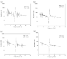
次に、図1(a)および(b)に示す弾性波デバイス10について、様々に条件を変えたときの周波数特性を求めた。まず、図1(a)に示す弾性波デバイス10を、すだれ状電極12aを波長1.2μm、厚み0.1波長のCu電極とし、圧電基板11を(0°,85°,0°)LN(厚み0.2波長)とし、音響多層膜13を、Al膜から成る低音響インピーダンス膜13a(厚み0.06波長)と、W膜から成る高音響インピーダンス膜13b(厚み0.06波長)とを交互に計6層積層したものとし、支持基板14をSi基板としたときの周波数特性を、図4(a)に示す。また、図1(b)に示す弾性波デバイス10が、すだれ状電極12aを、波長1.2μm、厚み0.1波長のCu電極12とし、圧電基板11を(90°,90°,42.5°)LN(厚み0.2波長)とし、浮き電極12bをAl電極とし、音響多層膜13を、SiO2膜から成る低音響インピーダンス膜13a(厚み0.05波長)と、Ta膜から成る高音響インピーダンス膜13b(厚み0.05波長)とを交互に計6層積層したものとし、支持基板14をSi基板としたときの周波数特性を、図4(b)に示す。
また、図1(a)に示す弾性波デバイス10を、すだれ状電極12aを波長1.2μm、厚み0.1波長のCu電極とし、圧電基板11を(0°,85°,0°)LT(厚み0.15波長)とし、音響多層膜13を、Al膜から成る低音響インピーダンス膜13a(厚み0.05波長)と、W膜から成る高音響インピーダンス膜13b(厚み0.05波長)とを交互に計6層積層したものとし、支持基板14をSi基板としたときの周波数特性を、図4(c)に示す。また、図1(b)に示す弾性波デバイス10が、すだれ状電極12aを波長1.2μm、厚み0.1波長のCu電極とし、圧電基板11を(90°,90°,35°)LT(厚み0.15波長)とし、浮き電極12bをAl電極とし、音響多層膜13を、SiO2膜から成る低音響インピーダンス膜13a(厚み0.07波長)と、Ta膜から成る高音響インピーダンス膜13b(厚み0.07波長)とを交互に計6層積層したものとし、支持基板14をSi基板としたときの周波数特性を、図4(d)に示す。なお、図1(a)に示す浮き電極12bがない場合には、圧電基板11に接するAl膜の表面が、絶縁膜化されたアルマイト膜であることが好ましい。
図4(a)~(d)に示すように、いずれの周波数特性も、1~5GHzでのSAWの基本モードやスプリアスの大きさが、図3の基本モードに比べ非常に小さくなっていることが確認された。一方で、9~11GHzのオーバートーンのレスポンスは大きく、3.2~8.1%の帯域、および、71~76dBのインピーダンス比が得られることが確認された。このオーバートーンの周波数は、音速12,000~13,000m/sに相当し、図2に示す基本モードの3.1倍の周波数である。
以下では、良好な特性を有するオーバートーンを得るために、様々に条件を変えたときの結果を示す。
以下では、良好な特性を有するオーバートーンを得るために、様々に条件を変えたときの結果を示す。
[LN基板を用いたとき]
図1(a)に示す弾性波デバイス10を、すだれ状電極12aを波長1.2μm、厚み0.1波長のCu電極とし、圧電基板11を(0°,θ,0°)LN(厚み0.2波長)とし、音響多層膜13を、Al膜から成る低音響インピーダンス膜13a(厚み0.05波長)と、W膜から成る高音響インピーダンス膜13b(厚み0.05波長)とを交互に計6層積層したものとし、支持基板14をSi基板とした構造(以下では、Cu(0.1λ)/(0°,θ,0°)LN(0.2λ)/Al(0.05λ)/W(0.05λ)/Al(0.05λ)/W(0.05λ)/Al(0.05λ)/W(0.05λ)/Si基板、のように記載する)のときの、帯域(Bandwidth)およびインピーダンス比(Impedance ratio)のオイラー角θに対する依存性を、それぞれ図5(a)および(b)に示す。なお、音響多層膜13の第1層目のAl膜の圧電基板側の表面は、絶縁のアルマイト処理されている、あるいは、SiO2膜などの絶縁性低音響インピーダンス膜が使用されていることが望ましい。特に断らない限り、音響多層膜13の第1層目のAl膜に接した浮き電極12bがない場合には、以下の実施例の1層目のAl膜表面は、アルマイト処理されているものとする。図5(a)および(b)に示すように、θ=60°~103°で、3%以上の帯域および60dB以上のインピーダンス比が得られることが確認された。また、インピーダンス比は、θ=72°~97°で65dB以上、θ=78°~92°で70dB以上であることが確認された。
図1(a)に示す弾性波デバイス10を、すだれ状電極12aを波長1.2μm、厚み0.1波長のCu電極とし、圧電基板11を(0°,θ,0°)LN(厚み0.2波長)とし、音響多層膜13を、Al膜から成る低音響インピーダンス膜13a(厚み0.05波長)と、W膜から成る高音響インピーダンス膜13b(厚み0.05波長)とを交互に計6層積層したものとし、支持基板14をSi基板とした構造(以下では、Cu(0.1λ)/(0°,θ,0°)LN(0.2λ)/Al(0.05λ)/W(0.05λ)/Al(0.05λ)/W(0.05λ)/Al(0.05λ)/W(0.05λ)/Si基板、のように記載する)のときの、帯域(Bandwidth)およびインピーダンス比(Impedance ratio)のオイラー角θに対する依存性を、それぞれ図5(a)および(b)に示す。なお、音響多層膜13の第1層目のAl膜の圧電基板側の表面は、絶縁のアルマイト処理されている、あるいは、SiO2膜などの絶縁性低音響インピーダンス膜が使用されていることが望ましい。特に断らない限り、音響多層膜13の第1層目のAl膜に接した浮き電極12bがない場合には、以下の実施例の1層目のAl膜表面は、アルマイト処理されているものとする。図5(a)および(b)に示すように、θ=60°~103°で、3%以上の帯域および60dB以上のインピーダンス比が得られることが確認された。また、インピーダンス比は、θ=72°~97°で65dB以上、θ=78°~92°で70dB以上であることが確認された。
図1(a)に示す弾性波デバイス10が、Cu(0.1λ)/(φ,85°,0°)LN(0.2λ)/Al(0.05λ)/W(0.05λ)/Al(0.05λ)/W(0.05λ)/Al(0.05λ)/W(0.05λ)/Si基板のときの、インピーダンス比のオイラー角φに対する依存性を、図6に示す。図6に示すように、φ=-30°~30°で、70dB以上のインピーダンス比が得られることが確認された。
図1(a)に示す弾性波デバイス10が、Cu(0.1λ)/(0°,85°,ψ)LN(0.2λ)/Al(0.05λ)/W(0.05λ)/Al(0.05λ)/W(0.05λ)/Al(0.05λ)/W(0.05λ)/Si基板のときの、インピーダンス比のオイラー角ψに対する依存性を、図7に示す。図7に示すように、ψ=-15°~15°で65dB以上、ψ=-6°~6°で70dB以上インピーダンス比が得られることが確認された。
図5~7の結果から、図1(a)に示す弾性波デバイス10では、圧電基板11として、(-30°~30°,60°~103°,-15°~15°)LNを用いることにより、3%以上の帯域および60dB以上のインピーダンス比が得られることがわかる。さらに、(-30°~30°,72°~97°,-15°~15°)LNを用いることにより、65dB以上のインピーダンス比が得られ、(-30°~30°,78°~92°,-6°~6°)LNを用いることにより、70dB以上のインピーダンス比が得られることがわかる。
図1(a)に示す弾性波デバイス10が、Cu(0.1λ)/(0°,85°,0°)LN(0.2λ)/Al膜/W膜/Al膜/W膜/Al膜/W膜/Si基板であって、Al膜厚を0.05波長として、高音響インピーダンス膜13bのW膜の膜厚を変化させたときの、インピーダンス比のW膜厚に対する依存性を、図8(a)に示す。また、W膜厚を0.05波長として、低音響インピーダンス膜13aのAl膜の膜厚を変化させたときの、インピーダンス比のAl膜厚に対する依存性を、図8(b)に示す。
図8(a)に示すように、高音響インピーダンス膜13bのW膜厚が0.026~0.108波長および0.12~0.187波長のとき、60dB以上のインピーダンス比が得られ、0.028~0.107波長および0.125~0.185波長のとき、65dB以上のインピーダンス比が得られ、0.035~0.102波長のとき、70dB以上のインピーダンス比が得られることが確認された。また、図示していないが、高音響インピーダンス膜13bのW膜厚が0.2波長以上でも大きなインピーダンス比が得られ、W膜厚が0.216~0.275波長のとき、60dB以上のインピーダンス比が得られ、W膜厚が0.22~0.27波長のとき、65dB以上のインピーダンス比が得られ、W膜厚が0.23~0.26波長で70dB以上のインピーダンス比が得られることが確認された。図8(a)では、Al膜厚が0.05波長のときの例を示したが、Al膜厚が0.02~0.118波長のときでも、最適なW膜厚は、Al膜厚が0.05波長のときと同じ膜厚を示した。
図8(b)に示すように、低音響インピーダンス膜13aのAl膜厚が0.02~0.118波長および0.129~0.185波長のとき、60dB以上のインピーダンス比が得られ、0.025~0.117波長および0.135~0.18波長のとき、65dB以上のインピーダンス比が得られ、0.04~0.113波長のとき、70dB以上のインピーダンス比が得られることが確認された。また、図示していないが、低音響インピーダンス膜13aのAl膜厚が0.2波長以上でも大きなインピーダンス比が得られ、Al膜厚が0.216~0.275波長のとき、60dB以上のインピーダンス比が得られ、Al膜厚が0.22~0.27波長のとき、65dB以上のインピーダンス比が得られ、Al膜厚が0.225~0.254波長のとき、70dB以上のインピーダンス比が得られることか確認された。図8(b)では、W膜厚が0.05波長のときの例を示したが、W膜厚が0.02~0.118波長のときでも、最適なAl膜厚は、W膜厚が0.05波長のときと同じ膜厚を示した。
図1(b)に示す弾性波デバイス10が、Cu(0.1λ)/(0°,θ,0°)LN(0.2λ)/浮き電極/Al(0.05λ)/W(0.05λ)/Al(0.05λ)/W(0.05λ)/Al(0.05λ)/W(0.05λ)/Si基板のときの、帯域およびインピーダンス比のオイラー角θに対する依存性を、それぞれ図9(a)および(b)に示す。なお、音響多層膜13の第1層目のAl膜は、表面が絶縁のアルマイト処理されている。アルマイト処理されていないAl電極を第1層目に用いるときは、第1層目のAl膜を浮き電極と兼用してもよい。図9(a)および(b)に示すように、θ=64°~98°で4%以上の帯域および60dB以上のインピーダンス比が得られ、θ=68°~95°で65dB以上のインピーダンス比が得られ、θ=72°~92°で70dB以上のインピーダンス比が得られることが確認された。
図1(b)に示す弾性波デバイス10が、Cu(0.1λ)/(0°,85°,0°)LN(0.2λ)/浮き電極/Al膜/W膜/Al膜/W膜/Al膜/W膜/Si基板であって、Al膜厚を0.05波長として、高音響インピーダンス膜13bのW膜の膜厚を変化させたときの、インピーダンス比のW膜厚に対する依存性を、図10(a)に示す。また、W膜厚を0.05波長として、低音響インピーダンス膜13aのAl膜の膜厚を変化させたときの、インピーダンス比のAl膜厚に対する依存性を、図10(b)に示す。
図10(a)に示すように、高音響インピーダンス膜13bのW膜厚が0.02~0.105波長および0.121~0.183波長のとき、60dB以上のインピーダンス比が得られ、0.027~0.103波長および0.124~0.18波長のとき、65dB以上のインピーダンス比が得られ、0.036~0.095波長のとき、70dB以上のインピーダンス比が得られることが確認された。また、図示していないが、高音響インピーダンス膜13bのW膜厚が0.2波長以上でも大きなインピーダンス比が得られ、W膜厚が0.216~0.275波長のとき、60dB以上のインピーダンス比が得られ、W膜厚が0.22~0.27波長のとき、65dB以上のインピーダンス比が得られ、W膜厚が0.23~0.26波長のとき、70dB以上のインピーダンス比が得られることが確認された。図10(a)では、Al膜厚が0.05波長のときの例を示したが、Al膜厚が0.02~0.113波長のときでも、最適なW膜厚は、Al膜厚が0.05波長のときと同じ膜厚を示した。
図10(b)に示すように、低音響インピーダンス膜13aのAl膜厚が0.02~0.113波長および0.132~0.185波長のとき、60dB以上のインピーダンス比が得られ、0.024~0.112波長および0.135~0.18波長のとき、65dB以上のインピーダンス比が得られ、0.038~0.104波長のとき、70dB以上のインピーダンス比が得られることが確認された。また、図示していないが、低音響インピーダンス膜13aのAl膜厚が0.2波長以上でも大きなインピーダンス比が得られ、Al膜厚が0.216~0.275波長のとき、60dB以上のインピーダンス比が得られ、Al膜厚が0.22~0.27波長のとき、65dB以上のインピーダンス比が得られ、Al膜厚が0.225~0.254波長のとき、70dB以上のインピーダンス比が得られることが確認された。図10(b)では、W膜厚が0.05波長のときの例を示したが、W膜厚が0.02~0.105波長のときでも、最適なAl膜厚は、W膜厚が0.05波長のときと同じ膜厚を示した。
図1(a)に示す弾性波デバイス10が、Cu(0.1λ)/(90°,90°,ψ)LN(0.2λ)/Al(0.05λ)/W(0.05λ)/Al(0.05λ)/W(0.05λ)/Al(0.05λ)/W(0.05λ)/Si基板のときの、帯域およびインピーダンス比のオイラー角ψに対する依存性を、それぞれ図11(a)および(b)に示す。図11(a)および(b)に示すように、ψ=160°~180°および0°~48°、すなわち、-20°~48°で7%以上の帯域および60dB以上のインピーダンス比が得られ、ψ=170°~180°および0°~43°、すなわち、-10°~43°で65dB以上のインピーダンス比が得られ、ψ=178°~180°および0°~33°、すなわち、-2°~33°で70dB以上のインピーダンス比が得られることが確認された。また、オイラー角φとθに関しては図示していないが、±6°でほぼ同じ値が得られ、(90°±6°,90°±6°,-20°~48°)で60dB以上のインピーダンス比が得られ、(90°±6°,90°±6°,-10°~43°)で65dB以上のインピーダンス比が得られ、(90°±6°,90°±6°,-2°~33°)で70dB以上のインピーダンス比が得られることが確認された。
図1(a)に示す弾性波デバイス10が、Cu(0.1λ)/(90°,90°,42.5°)LN(0.2λ)/Al膜/W膜/Al膜/W膜/Al膜/W膜/Si基板であって、Al膜厚を0.05波長として、高音響インピーダンス膜13bのW膜の膜厚を変化させたときの、インピーダンス比のW膜厚に対する依存性を、図12(a)に示す。また、W膜厚を0.05波長として、低音響インピーダンス膜13aのAl膜の膜厚を変化させたときの、インピーダンス比のAl膜厚に対する依存性を、図12(b)に示す。
図12(a)に示すように、高音響インピーダンス膜13bのW膜厚が0.015~0.104波長および0.12~0.183波長のとき、60dB以上のインピーダンス比が得られ、0.018~0.101波長および0.123~0.181波長のとき、65dB以上のインピーダンス比が得られ、0.024~0.097波長のとき、70dB以上のインピーダンス比が得られることが確認された。また、図示していないが、高音響インピーダンス膜13bのW膜厚が0.2波長以上でも大きなインピーダンス比が得られ、W膜厚が0.216~0.275波長のとき、60dB以上のインピーダンス比が得られ、W膜厚が0.22~0.27波長のとき、65dB以上のインピーダンス比が得られ、W膜厚が0.23~0.26波長のとき、70dB以上のインピーダンス比が得られることが確認された。図12(a)では、Al膜厚が0.05波長のときの例を示したが、Al膜厚が0.014~0.113波長のときでも、最適なW膜厚は、Al膜厚が0.05波長のときと同じ膜厚を示した。
図12(b)に示すように、低音響インピーダンス膜13aのAl膜厚が0.014~0.113波長および0.124~0.182波長のとき、60dB以上のインピーダンス比が得られ、0.016~0.109波長および0.13~0.176波長のとき、65dB以上のインピーダンス比が得られ、0.022~0.104波長のとき、70dB以上のインピーダンス比が得られることが確認された。また、図示していないが、低音響インピーダンス膜13aのAl膜厚が0.2波長以上でも大きなインピーダンス比が得られ、Al膜厚が0.216~0.275波長のとき、60dB以上のインピーダンス比が得られ、Al膜厚が0.22~0.27波長のとき、65dB以上のインピーダンス比が得られ、Al膜厚が0.225~0.254波長のとき、70dB以上のインピーダンス比が得られることが確認された。図12(b)では、W膜厚が0.05波長のときの例を示したが、W膜厚が0.015~0.104波長のときでも、最適なAl膜厚は、W膜厚が0.05波長のときと同じ膜厚を示した。
図1(b)に示す弾性波デバイス10が、Cu(0.1λ)/(90°,90°,ψ)LN(0.2λ)/浮き電極/SiO2(0.05λ)/Ta(0.05λ)/SiO2(0.05λ)/Ta(0.05λ)/SiO2(0.05λ)/Ta(0.05λ)/Si基板のときの、帯域およびインピーダンス比のオイラー角ψに対する依存性を、それぞれ図13(a)および(b)に示す。図13(a)および(b)に示すように、ψ=176°~180°および0°~56°、すなわち、-4°~56°で7%以上の帯域および65dB以上のインピーダンス比が得られ、ψ=178°~180°および0°~52°、すなわち、-2°~52°で70dB以上のインピーダンス比が得られ、ψ=25°~50°で75dB以上のインピーダンス比が得られることが確認された。
また、オイラー角φとθに関しては図示していないが、±6°でほぼ同じ値が得られ、(90°±6°,90°±6°,-4°~56°)で65dB以上のインピーダンス比が得られ、(90°±6°,90°±6°,-2°~52°)で70dB以上のインピーダンス比が得られ、(90°±6°,90°±6°,25°~50°)で75dB以上のインピーダンス比が得られることが確認された。
図1(b)に示す弾性波デバイス10が、Cu(0.1λ)/(90°,90°,42.5°)LN(0.2λ)/浮き電極/SiO2膜/Ta膜/SiO2膜/Ta膜/SiO2膜/Ta膜/Si基板であって、SiO2膜厚を0.05波長として、高音響インピーダンス膜13bのTa膜の膜厚を変化させたときの、インピーダンス比のTa膜厚に対する依存性を、図14(a)に示す。また、Ta膜厚を0.05波長として、低音響インピーダンス膜13aのSiO2膜の膜厚を変化させたときの、インピーダンス比のSiO2膜厚に対する依存性を、図14(b)に示す。
図14(a)に示すように、高音響インピーダンス膜13bのTa膜厚が0.015~0.1波長、0.118~0.175波長、および0.216~0.275波長のとき、60dB以上のインピーダンス比が得られ、0.017~0.093波長、0.12~0.17波長、および0.22~0.27波長のとき、65dB以上のインピーダンス比が得られ、0.02~0.087波長、0.125~0.165波長、および0.23~0.26波長のとき、70dB以上のインピーダンス比が得られ、0.036~0.082波長のとき75dB以上のインピーダンス比が得られることが確認された。図14(a)では、SiO2膜厚が0.05波長のときの例を示したが、SiO2膜厚が0.012~0.096波長のときでも、最適なTa膜厚は、SiO2膜厚が0.05波長のときと同じ膜厚を示した。
また、図14(b)に示すように、低音響インピーダンス膜13aのSiO2膜厚が0.012~0.096波長、0.12~0.185波長、および0.216~0.275波長のとき、60dB以上のインピーダンス比が得られ、0.015~0.092波長、0.125~0.18波長、および0.22~0.27波長のとき、65dB以上のインピーダンス比が得られ、0.02~0.087波長、0.133~0.172波長、および0.225~0.254波長のとき70dB以上のインピーダンス比が得られ、0.04~0.07波長のとき75dB以上のインピーダンス比が得られることが確認された。図14(b)では、Ta膜厚が0.05波長のときの例を示したが、Ta膜厚が0.015~0.1波長のときでも、最適なSiO2膜厚は、Ta膜厚が0.05波長のときと同じ膜厚を示した。
[LT基板を用いたとき]
図1(a)に示す弾性波デバイス10が、Cu(0.1λ)/(0°,θ,0°)LT(0.15λ)/Al(0.05λ)/W(0.05λ)/Al(0.05λ)/W(0.05λ)/Al(0.05λ)/W(0.05λ)/Si基板のときの、帯域およびインピーダンス比のオイラー角θに対する依存性を、それぞれ図15(a)および(b)に示す。図15(a)および(b)に示すように、θ=55°~100°で2%以上の帯域および60dB以上のインピーダンス比が得られ、θ=61°~95°で65dB以上のインピーダンス比が得られ、θ=70°~89°で70dB以上のインピーダンス比が得られることが確認された。
図1(a)に示す弾性波デバイス10が、Cu(0.1λ)/(0°,θ,0°)LT(0.15λ)/Al(0.05λ)/W(0.05λ)/Al(0.05λ)/W(0.05λ)/Al(0.05λ)/W(0.05λ)/Si基板のときの、帯域およびインピーダンス比のオイラー角θに対する依存性を、それぞれ図15(a)および(b)に示す。図15(a)および(b)に示すように、θ=55°~100°で2%以上の帯域および60dB以上のインピーダンス比が得られ、θ=61°~95°で65dB以上のインピーダンス比が得られ、θ=70°~89°で70dB以上のインピーダンス比が得られることが確認された。
また、LTの結晶構造は、LNの結晶構造と同じであるため、(φ,θ,ψ)LTにおけるφやψの関係も、LNと同じであった。このため、LTの場合も、(-30°~30°,55°~100°,-15°~15°)LTで60dB以上のインピーダンス比が得られ、(-30°~30°,61°~95°,-15°~15°)LTで65dB以上のインピーダンス比が得られ、(-30°~30°,70°~89°,-6°~6°)LTで70dB以上のインピーダンス比が得られる。
図1(a)に示す弾性波デバイス10が、Cu(0.1λ)/(0°,85°,0°)LT(0.15λ)/Al膜/W膜/Al膜/W膜/Al膜/W膜/Si基板であって、Al膜厚を0.05波長として、高音響インピーダンス膜13bのW膜の膜厚を変化させたときの、インピーダンス比のW膜厚に対する依存性を、図16(a)に示す。また、W膜厚を0.05波長として、低音響インピーダンス膜13aのAl膜の膜厚を変化させたときの、インピーダンス比のAl膜厚に対する依存性を、図16(b)に示す。
図16(a)に示すように、高音響インピーダンス膜13bのW膜厚が0.02~0.10波長および0.115~0.2波長のとき、60dB以上のインピーダンス比が得られ、0.025~0.095波長および0.117~0.19波長のとき、65dB以上のインピーダンス比が得られ、0.03~0.092波長および0.12~0.17波長のとき、70dB以上のインピーダンス比が得られることが確認された。また、図示していないが、高音響インピーダンス膜13bのW膜厚が0.2波長以上でも大きなインピーダンス比が得られ、W膜厚が0.216~0.275波長のとき、60dB以上のインピーダンス比が得られ、W膜厚が0.22~0.27波長のとき、65dB以上のインピーダンス比が得られ、W膜厚が0.225~0.26波長のとき、70dB以上のインピーダンス比が得られることが確認された。図16(a)では、Al膜厚が0.05波長のときの例を示したが、Al膜厚が0.02~0.1波長のときでも、最適なW膜厚は、Al膜厚が0.05波長のときと同じ膜厚を示した。
図16(b)に示すように、低音響インピーダンス膜13aのAl膜厚が0.02~0.1波長および0.115~0.2波長のとき、60dB以上のインピーダンス比が得られ、0.025~0.095波長および0.12~0.19波長のとき、65dB以上のインピーダンス比が得られ、0.03~0.12波長および0.12~0.15波長のとき、70dB以上のインピーダンス比が得られることが確認された。また、図示していないが、高音響インピーダンス膜13bのAl膜厚が0.2波長以上でも大きなインピーダンス比が得られ、Al膜厚が0.216~0.275波長のとき、60dB以上のインピーダンス比が得られ、Al膜厚が0.22~0.27波長のとき、65dB以上のインピーダンス比が得られ、Al膜厚が0.225~0.26波長のとき、70dB以上のインピーダンス比が得られることが確認された。図16(b)では、W膜厚が0.05波長のときの例を示したが、W膜厚が0.02~0.1波長のときでも、最適なAl膜厚は、W膜厚が0.05波長のときと同じ膜厚を示した。
図1(b)に示す弾性波デバイス10が、Cu(0.1λ)/(0°,θ,0°)LT(0.15λ)/浮き電極/Al(0.05λ)/W(0.05λ)/Al(0.05λ)/W(0.05λ)/Al(0.05λ)/W(0.05λ)/Si基板のとき、および、Cu(0.1λ)/(0°,θ,0°)LT(0.15λ)/浮き電極/SiO2(0.05λ)/Ta(0.05λ)/SiO2(0.05λ)/Ta(0.05λ)/SiO2(0.05λ)/Ta(0.05λ)/Si基板のときの、帯域およびインピーダンス比のオイラー角θに対する依存性を、それぞれ図17(a)および(b)に示す。図17(a)および(b)に示すように、低音響インピーダンス膜13aと高音響インピーダンス膜13bの組み合わせが、Al膜とW膜の場合と、SiO2膜とTa膜の場合とで、帯域およびインピーダンス比のθ依存性には、ほとんど差がないことが確認された。また、いずれの組み合わせの場合も、θ=65°~94°で2%以上の帯域および60dB以上のインピーダンス比が得られ、θ=69°~91°で65dB以上のインピーダンス比が得られることが確認された。
図1(b)に示す弾性波デバイス10が、Cu(0.1λ)/(0°,85°,0°)LT(0.15λ)/浮き電極/Al膜/W膜/Al膜/W膜/Al膜/W膜/Si基板であって、Al膜厚を0.05波長として、高音響インピーダンス膜13bのW膜の膜厚を変化させたときの、インピーダンス比のW膜厚に対する依存性を、図18(a)に示す。また、W膜厚を0.05波長として、低音響インピーダンス膜13aのAl膜の膜厚を変化させたときの、インピーダンス比のAl膜厚に対する依存性を、図18(b)に示す。
図18(a)に示すように、高音響インピーダンス膜13bのW膜厚が0.023~0.097波長および0.116~0.194波長のとき、60dB以上のインピーダンス比が得られ、0.028~0.093波長および0.118~0.18波長のとき、65dB以上のインピーダンス比が得られることが確認された。また、図示していないが、高音響インピーダンス膜13bのW膜厚が0.2波長以上でも大きなインピーダンス比が得られ、W膜厚が0.216~0.275波長のとき、60dB以上のインピーダンス比が得られ、W膜厚が0.22~0.27波長のとき、65dB以上のインピーダンス比が得られることが確認された。図18(a)では、Al膜厚が0.05波長のときの例を示したが、Al膜厚が0.023~0.098波長のときでも、最適なW膜厚は、Al膜厚が0.05波長のときと同じ膜厚を示した。
図18(b)に示すように、低音響インピーダンス膜13aのAl膜厚が0.023~0.098波長および0.125~0.193波長のとき、60dB以上のインピーダンス比が得られ、0.028~0.094波長および0.135~0.185波長のとき、65dB以上のインピーダンス比が得られることが確認された。また、図示していないが、高音響インピーダンス膜13bのAl膜厚が0.2波長以上でも大きなインピーダンス比が得られ、Al膜厚が0.216~0.275波長のとき、60dB以上のインピーダンス比が得られ、Al膜厚が0.22~0.27波長のとき、65dB以上のインピーダンス比が得られることが確認された。図18(b)では、W膜厚が0.05波長のときの例を示したが、W膜厚が0.023~0.097波長のときでも、最適なAl膜厚は、W膜厚が0.05波長のときと同じ膜厚を示した。
図1(a)に示す弾性波デバイス10が、Cu(0.1λ)/(90°,90°,ψ)LT(0.15λ)/Al(0.05λ)/W(0.05λ)/Al(0.05λ)/W(0.05λ)/Al(0.05λ)/W(0.05λ)/Si基板のときの、帯域およびインピーダンス比のオイラー角θに対する依存性を、それぞれ図19(a)および(b)に示す。図19(a)および(b)に示すように、ψ=175°~180°、0°~61°、および、83°~93°、すなわち、ψ=-5°~61°および83°~93°で、2.3%以上の帯域および65dB以上のインピーダンス比が得られ、ψ=15°~55°および85°~91°で、70dB以上のインピーダンス比が得られ、ψ=23°~38°で75dB以上のインピーダンス比が得られることが確認された。
また、オイラー角φとθに関しては図示していないが、±6°でほぼ同じ値が得られ、(90°±6°,90°±6°,-5°~61°)および(90°±6°,90°±6°,83°~93°)で、65dB以上のインピーダンス比が得られ、(90°±6°,90°±6°,15°~55°)および(90°±6°,90°±6°,85°~91°)で、70dB以上のインピーダンス比が得られ、(90°±6°,90°±6°,23°~83°)で75dB以上のインピーダンス比が得られることが確認された。
図1(a)に示す弾性波デバイス10が、Cu(0.1λ)/(90°,90°,35°)LT(0.15λ)/Al膜/W膜/Al膜/W膜/Al膜/W膜/Si基板であって、Al膜厚を0.05波長として、高音響インピーダンス膜13bのW膜の膜厚を変化させたときの、インピーダンス比のW膜厚に対する依存性を、図20(a)に示す。また、W膜厚を0.05波長として、低音響インピーダンス膜13aのAl膜の膜厚を変化させたときの、インピーダンス比のAl膜厚に対する依存性を、図20(b)に示す。
図20(a)に示すように、高音響インピーダンス膜13bのW膜厚が0.016~0.08波長および0.105~0.172波長のとき、65dB以上のインピーダンス比が得られ、0.02~0.074波長および0.114~0.16波長のとき、70dB以上のインピーダンス比が得られ、0.03~0.067波長のとき75dB以上のインピーダンス比が得られることが確認された。また、図示していないが、高音響インピーダンス膜13bのW膜厚が0.2波長以上でも大きなインピーダンス比が得られ、W膜厚が0.216~0.275波長のとき、60dB以上のインピーダンス比が得られ、W膜厚が0.22~0.27波長のとき、65dB以上のインピーダンス比が得られ、W膜厚が0.225~0.26波長のとき、70dB以上のインピーダンス比が得られることが確認された。図20(a)では、Al膜厚が0.05波長のときの例を示したが、Al膜厚が0.018~0.08波長のときでも、最適なW膜厚は、Al膜厚が0.05波長のときと同じ膜厚を示した。
図20(b)に示すように、低音響インピーダンス膜13aのAl膜厚が0.018~0.08波長および0.106~0.17波長のとき、65dB以上のインピーダンス比が得られ、0.022~0.076波長および0.117~0.16波長のとき、70dB以上のインピーダンス比が得られ、0.032~0.07波長のとき75dB以上のインピーダンス比が得られることが確認された。また、図示していないが、高音響インピーダンス膜13bのAl膜厚が0.2波長以上でも大きなインピーダンス比が得られ、Al膜厚が0.216~0.275波長のとき、60dB以上のインピーダンス比が得られ、Al膜厚が0.22~0.27波長のとき、65dB以上のインピーダンス比が得られ、Al膜厚が0.225~0.26波長のとき、70dB以上のインピーダンス比が得られることが確認された。図20(b)では、W膜厚が0.05波長のときの例を示したが、W膜厚が0.016~0.08波長のときでも、最適なAl膜厚は、W膜厚が0.05波長のときと同じ膜厚を示した。
図1(b)に示す弾性波デバイス10が、Cu(0.1λ)/(90°,90°,ψ)LT(0.15λ)/浮き電極/SiO2(0.05λ)/Ta(0.05λ)/SiO2(0.05λ)/Ta(0.05λ)/SiO2(0.05λ)/Ta(0.05λ)/Si基板のときの、帯域およびインピーダンス比のオイラー角ψに対する依存性を、それぞれ図21(a)および(b)に示す。図21(a)および(b)に示すように、ψ=176°~180°および0°~56°、すなわち、-4°~56°で7%以上の帯域および65dB以上のインピーダンス比が得られ、ψ=178°~180°および0°~52°、すなわち、-2°~52°で70dB以上のインピーダンス比が得られ、ψ=25°~50°で75dB以上のインピーダンス比が得られることが確認された。
また、オイラー角φとθに関しては図示していないが、±6°でほぼ同じ値が得られ、(90°±6°,90°±6°,-4°~56°)で65dB以上のインピーダンス比が得られ、(90°±6°,90°±6°,-2°~52°)で70dB以上のインピーダンス比が得られ、(90°±6°,90°±6°,25°~50°)で75dB以上のインピーダンス比が得られることが確認された。
図1(b)に示す弾性波デバイス10が、Cu(0.1λ)/(90°,90°,35°)LT(0.15λ)/浮き電極/SiO2膜/Ta膜/SiO2膜/Ta膜/SiO2膜/Ta膜/Si基板であって、SiO2膜厚を0.05波長として、高音響インピーダンス膜13bのTa膜の膜厚を変化させたときの、インピーダンス比のTa膜厚に対する依存性を、図22(a)に示す。また、Ta膜厚を0.05波長として、低音響インピーダンス膜13aのSiO2膜の膜厚を変化させたときの、インピーダンス比のSiO2膜厚に対する依存性を、図22(b)に示す。
図22(a)に示すように、高音響インピーダンス膜13bのTa膜厚が0.015~0.085波長、0.105~0.183波長、および0.216~0.275波長のとき、60dB以上のインピーダンス比が得られ、0.018~0.08波長、0.107~0.175波長、および0.22~0.27波長のとき、65dB以上のインピーダンス比が得られ、0.02~0.075波長、0.115~0.165波長、および0.225~0.26波長のとき、70dB以上のインピーダンス比が得られ、0.034~0.065波長のとき75dB以上のインピーダンス比が得られることが確認された。図22(a)では、SiO2膜厚が0.05波長のときの例を示したが、SiO2膜厚が0.015~0.085波長のときでも、最適なTa膜厚は、SiO2膜厚が0.05波長のときと同じ膜厚を示した。
また、図22(b)に示すように、低音響インピーダンス膜13aのSiO2膜厚が0.015~0.085波長、0.118~0.18波長、および0.216~0.275波長のとき、60dB以上のインピーダンス比が得られ、0.017~0.093波長、0.122~0.175波長、および0.22~0.27波長のとき、65dB以上のインピーダンス比が得られ、0.02~0.087波長、0.13~0.17波長、および0.225~0.26波長のとき、70dB以上のインピーダンス比が得られ、0.035~0.08波長のとき75dB以上のインピーダンス比が得られることが確認された。図20(b)では、Ta膜厚が0.05波長のときの例を示したが、Ta膜厚が0.015~0.085波長のときでも、最適なSiO2膜厚は、Ta膜厚が0.05波長のときと同じ膜厚を示した。
図1(b)に示す弾性波デバイス10が、Cu(0.1λ)/(90°,90°,42.5°)LN(0.2λ)/浮き電極/SiO2膜(0.05λ)/Ta膜(0.05λ)/SiO2膜(0.05λ)/Ta膜(0.05λ)/SiO2膜(0.05λ)/Ta膜(0.05λ)/Si基板のとき、および、Cu(0.1λ)/(90°,90°,35°)LT(0.15λ)/浮き電極/SiO2膜(0.05λ)/Ta膜(0.05λ)/SiO2膜(0.05λ)/Ta膜(0.05λ)/SiO2膜(0.05λ)/Ta膜(0.05λ)/Si基板のときの、インピーダンス比の圧電基板11の厚さに対する依存性を、図23に示す。図23に示すように、LNおよびLTの厚みがそれぞれ5波長以下および2.4波長以下のとき、65dB以上のインピーダンス比が得られ、LNおよびLTの厚みがそれぞれ1.2波長以下および1波長以下のとき、70dB以上のインピーダンス比が得られ、LNおよびLTの厚みがそれぞれ0.3~0.02波長および0.25~0.02波長のとき、75dB以上のインピーダンス比が得られることが確認された。
図1(b)に示す弾性波デバイス10が、Cu(0.1λ)/(90°,90°,35°)LT(0.15λ)/浮き電極/SiO2膜(0.05λ)/Ta膜(0.05λ)/SiO2膜(0.05λ)/Ta膜(0.05λ)/SiO2膜(0.05λ)/Ta膜(0.05λ)/Si基板のときの、インピーダンス比の音響多層膜13の層数に対する依存性を、図24に示す。図24に示すように、音響多層膜13が3層のとき65dBのインピーダンス比が得られ、4層のとき72dBのインピーダンス比が得られ、5層のとき74dBのインピーダンス比が得られ、6~30層のとき76dBのインピーダンス比が得られることが確認された。なお、音響多層膜13の各膜を成膜する際に、接着強度を強くするために設けられたTiなどの膜は、膜厚が数十nmから数百nmであり、音響多層膜13の各膜と比べて相対的に非常に薄いため、音響インピーダンス膜としては含んでいない。
図1(b)に示す弾性波デバイス10が、すだれ状電極12a/(90°,90°,35°)LT(0.15λ)/浮き電極/SiO2膜(0.05λ)/Ta膜(0.05λ)/SiO2膜(0.05λ)/Ta膜(0.05λ)/SiO2膜(0.05λ)/Ta膜(0.05λ)/Si基板のときの、インピーダンス比のすだれ状電極12aの電極12厚に対する依存性を、図25に示す。なお、図25では、すだれ状電極12aのメタライゼーション比(MR)を、0.5とし、すだれ状電極12aとして、Cu電極、Al電極、Au電極、Mo電極を使用したときの結果を示す。
図25に示すように、Cu電極では、電極厚が0.01~0.033波長および0.06~0.2波長のとき、65dB以上のインピーダンス比が得られ、電極厚が0.014~0.03波長および0.07~0.18波長のとき、70dB以上のインピーダンス比が得られ、電極厚が0.1~0.14波長のとき75dB以上のインピーダンス比が得られることが確認された。また、Al電極では、電極厚が0.01~0.045波長および0.1~0.21波長のとき、65dB以上のインピーダンス比が得られ、電極厚が0.02~0.041波長および0.135~0.197波長のとき、70dB以上のインピーダンス比が得られ、電極厚が0.159~0.182波長のとき75dB以上のインピーダンス比が得られることが確認された。
また、Au電極では、電極厚が0.005~0.02波長および0.062~0.165波長のとき、65dB以上のインピーダンス比が得られ、電極厚が0.01~0.0152波長および0.064~0.155波長のとき、70dB以上のインピーダンス比が得られ、電極厚が0.08~0.12波長のとき75dB以上のインピーダンス比が得られることが確認された。また、Mo電極では、電極厚が0.008~0.03波長および0.055~0.19波長のとき、65dB以上のインピーダンス比が得られ、電極厚が0.0125~0.027波長および0.065~0.165波長のとき、70dB以上のインピーダンス比が得られ、電極厚が0.095~0.13波長のとき、75dB以上のインピーダンス比が得られることが確認された。
なお、すだれ状電極12aは、密度が1800kg/m3以上6000kg/m3未満のとき、Al電極と同じ電極厚が最適厚となり、6000kg/m3以上10000kg/m3未満のとき、Cu電極と同じ電極厚が最適厚となり、10000kg/m3以上15000kg/m3未満のとき、Mo電極と同じ電極厚が最適厚となり、15000kg/m3以上25000kg/m3未満のとき、Au電極と同じ電極厚が最適厚となる。ここで、すだれ状電極12aが合金や多層金属膜から成る場合には、その平均密度で換算して、最適厚を決定する。すだれ状電極12aのメタライジェイション比(MR)が0.5からずれるときには、MRが0.5のときの最適厚をHとすると、H×0.5/MRが最適厚となる。
図1(b)に示す弾性波デバイス10が、Cu(0.1λ)/(90°,90°,42.5°)LN(0.2λ)/浮き電極/SiO2膜(0.05λ)/Ta膜(0.05λ)/SiO2膜(0.05λ)/Ta膜(0.05λ)/SiO2膜(0.05λ)/Ta膜(0.05λ)/Si基板のとき、および、Cu(0.1λ)/(90°,90°,35°)LT(0.15λ)/浮き電極/SiO2膜(0.05λ)/Ta膜(0.05λ)/SiO2膜(0.05λ)/Ta膜(0.05λ)/SiO2膜(0.05λ)/Ta膜(0.05λ)/Si基板のときの、インピーダンス比のすだれ状電極12aのMRに対する依存性を、図26に示す。図26に示すように、LNおよびLT共に、MRが0.35~0.8のとき、65dB以上のインピーダンス比が得られることが確認された。また、LNでは、MRが045~0.8のとき、70dB以上のインピーダンス比が得られ、LTでは、MRが0.45~0.6のとき、68dB以上のインピーダンス比が得られることが確認された。
[特許文献3との比較]
図3(a)に示す5.1GHz近傍で励振されている特性は、音速6,100m/sであり、LLSAWに相当している。これに対し、特許文献3では、0.05、0.06、0.08波長厚のAl電極を用いて、LLSAWを励振しているが、図25に示すように、Al電極のその厚みでは、SAWのオーバートーンを、大きく励振することはできない。
図3(a)に示す5.1GHz近傍で励振されている特性は、音速6,100m/sであり、LLSAWに相当している。これに対し、特許文献3では、0.05、0.06、0.08波長厚のAl電極を用いて、LLSAWを励振しているが、図25に示すように、Al電極のその厚みでは、SAWのオーバートーンを、大きく励振することはできない。
また、特許文献3に示す弾性波デバイスに相当する、Al(0.05λ)/0.2波長の(90°,90°,40°)LN(0.2λ)/音響多層膜[Multi acoustic layers;SiO2(0.25λ)/Ta(0.25λ)/SiO2(0.25λ)/Ta(0.25λ)/SiO2(0.25λ)/Ta(0.25λ)/SiO2(0.25λ)/Ta(0.25λ)]/Si基板の構造での、LLSAWに相当する音速6,200m/sの周波数特性の変位分布を、図27(a)に示す。図27(a)に示すように、その変異分布は、縦波成分(図中の「L」)が主であり、励振される振動が、特許文献3に示すLLSAWであることが確認された。
一方、図1(a)に示す弾性波デバイス10が、Cu(0.1λ)/(90°,90°,42.5°)LN(0.2λ)/音響多層膜[Multi acoustic layers;SiO2(0.05λ)/Ta(0.05λ)/SiO2(0.05λ)/Ta(0.05λ)/SiO2(0.05λ)/Ta(0.05λ)/SiO2(0.05λ)/Ta(0.05λ)]/Si基板のときの、音速11,000m/s近傍のオーバートーンの周波数特性の変位分布を、図27(b)に示す。図27(b)に示すように、その変異分布は、SH成分を主成分とするSAWであることが確認された。このように、特許文献3の弾性波デバイスと本発明の実施の形態の弾性波デバイス10とでは、周波数・音速の違い、LLSAWの基本モードとSAWのオーバートーンの違いに加え、変位分布が全く異なることから、振動モードも異なることが明らかである。
10 弾性波デバイス
11 圧電基板
12 電極
12a すだれ状電極
12b 浮き電極
13 音響多層膜
13a 低音響インピーダンス膜
13b 高音響インピーダンス膜
14 支持基板
11 圧電基板
12 電極
12a すだれ状電極
12b 浮き電極
13 音響多層膜
13a 低音響インピーダンス膜
13b 高音響インピーダンス膜
14 支持基板
Claims (17)
- 圧電基板と、
前記圧電基板に接するよう設けられた電極と、
前記圧電基板および/または前記電極に接するよう設けられた音響多層膜とを有し、
弾性表面波の共振特性のうちのオーバートーンを利用するよう構成されていることを
特徴とする弾性波デバイス。 - 前記オーバートーンの弾性表面波は、音速9000m/s以上に相当することを特徴とする請求項1記載の弾性波デバイス。
- 前記音響多層膜は、低音響インピーダンス膜と高音響インピーダンス膜とが交互に積層されていることを特徴とする請求項1または2記載の弾性波デバイス。
- 前記音響多層膜は、低音響インピーダンス膜と高音響インピーダンス膜とが交互に連続して3層以上20層以下で積層された音響膜を有することを特徴とする請求項1乃至3のいずれか1項に記載の弾性波デバイス。
- 前記音響多層膜の各低音響インピーダンス膜および/または各高音響インピーダンス膜は、Mg合金、SiO2、SiOF、Al、Y、Si、Ge、Ti、ZnO、SixNy(ここで、xおよびyは正の実数)、AlN、SiC、Al2O3、Ag、ZrO2、Hf、Cu、TiO2、Cr、Ni、Au、Ta、Mo、Pt、およびWのうちの少なくとも1つを含む膜、または、これらのうちの少なくとも1つを含む酸化膜、窒化膜、炭化膜もしくはヨウ化膜から成ることを特徴とする請求項3または4記載の弾性波デバイス。
- 前記音響多層膜の各低音響インピーダンス膜および各高音響インピーダンス膜のうち、少なくとも3層の各厚みが、それぞれ前記弾性表面波の0.012波長~0.118波長、0.105波長~0.2波長、または、0.216波長~0.275波長であることを特徴とする請求項3乃至5のいずれか1項に記載の弾性波デバイス。
- 前記音響多層膜の各低音響インピーダンス膜のうち少なくとも1層の厚みが、前記弾性表面波の0.012波長~0.118波長であり、各高音響インピーダンス膜のうち少なくとも1層の厚みが、前記弾性表面波の0.015波長~0.108波長、0.109波長~0.12波長、または、0.216波長~0.275波長であることを特徴とする請求項3乃至6のいずれか1項に記載の弾性波デバイス。
- 前記音響多層膜の各高音響インピーダンス膜のうち少なくとも1層の厚みが、前記弾性表面波の0.015波長~0.108波長であり、各低音響インピーダンス膜のうち少なくとも2層の各厚みが、それぞれ前記弾性表面波の0.015波長~0.118波長、0.119波長~0.2波長、または、0.216波長~0.275波長であることを特徴とする請求項3乃至6のいずれか1項に記載の弾性波デバイス。
- 前記圧電基板は、LiNbO3またはLiTaO3の単結晶から成ることを特徴とする請求項1乃至8のいずれか1項に記載の弾性波デバイス。
- 前記電極は、前記圧電基板の一方の表面に設けられたすだれ状電極から成り、
前記音響多層膜は、前記圧電基板の他方の表面に接するよう設けられ、
前記圧電基板は、LiNbO3結晶から成り、オイラー角が(-30°~30°,60°~103°,-15°~15°)および(90°±6°,90°±6°,-20°~48°)のいずれか一方、または、これらのいずれか一方と結晶学的に等価なオイラー角であることを
特徴とする請求項1乃至8のいずれか1項に記載の弾性波デバイス。 - 前記電極は、前記圧電基板の一方の表面に設けられたすだれ状電極と、前記圧電基板の他方の表面を覆うよう設けられた浮き電極とを有し、
前記音響多層膜は、前記浮き電極の前記圧電基板とは反対側の表面に接するよう設けられ、
前記圧電基板は、LiNbO3結晶から成り、オイラー角が(-30°~30°,64°~98°,-15°~15°)および(90°±6°,90°±6°,-4°~56°)のいずれか一方、または、これらのいずれか一方と結晶学的に等価なオイラー角であることを
特徴とする請求項1乃至8のいずれか1項に記載の弾性波デバイス。 - 前記圧電基板は、厚みが前記弾性表面波の0.002~5波長であることを特徴とする請求項10または11記載の弾性波デバイス。
- 前記電極は、前記圧電基板の一方の表面に設けられたすだれ状電極から成り、
前記音響多層膜は、前記圧電基板の他方の表面に接するよう設けられ、
前記圧電基板は、LiTaO3結晶から成り、オイラー角が(-30°~30°,55°~100°,-15°~15°)、(90°±6°,90°±6°,-5°~61°)および(90°±6°,90°±6°,83°~93°)のいずれか一つ、または、これらのいずれか一つと結晶学的に等価なオイラー角であることを
特徴とする請求項1乃至8のいずれか1項に記載の弾性波デバイス。 - 前記電極は、前記圧電基板の一方の表面に設けられたすだれ状電極と、前記圧電基板の他方の表面を覆うよう設けられた浮き電極とを有し、
前記音響多層膜は、前記浮き電極の前記圧電基板とは反対側の表面に接するよう設けられ、
前記圧電基板は、LiTaO3結晶から成り、オイラー角が(-30°~30°,65°~94°,-15°~15°)および(90°±6°,90°±6°,-4°~56°)のいずれか一方、または、これらのいずれか一方と結晶学的に等価なオイラー角であることを
特徴とする請求項1乃至8のいずれか1項に記載の弾性波デバイス。 - 前記圧電基板は、厚みが前記弾性表面波の0.002~2.4波長であることを特徴とする請求項13または14記載の弾性波デバイス。
- 前記すだれ状電極は、メタライジェイション比をMRとし、前記弾性表面波の波長をλとすると、密度が1800kg/m3以上6000kg/m3未満で、厚みが(0.01λ~0.045λ)×0.5/MRもしくは(0.1λ~0.21λ)×0.5/MR、または、密度が6000kg/m3以上10000kg/m3未満で、厚みが(0.01λ~0.033λ)×0.5/MRもしくは(0.06λ~0.2λ)×0.5/MR、または、密度が10000kg/m3以上15000kg/m3未満で、厚みが(0.008λ~0.03λ)×0.5/MRもしくは(0.055λ~0.19λ)×0.5/MR、または、密度が15000kg/m3以上25000kg/m3未満で、厚みが(0.005λ~0.02λ)×0.5/MRもしくは(0.062λ~0.165λ)×0.5/MRであることを特徴とする請求項10乃至15のいずれか1項に記載の弾性波デバイス。
- 前記すだれ状電極は、メタライジェイション比が0.35以上であることを特徴とする請求項10乃至15のいずれか1項に記載の弾性波デバイス。
Priority Applications (3)
| Application Number | Priority Date | Filing Date | Title |
|---|---|---|---|
| CN202180017384.6A CN115176416A (zh) | 2020-02-28 | 2021-02-12 | 弹性波器件 |
| JP2022503254A JPWO2021172032A1 (ja) | 2020-02-28 | 2021-02-12 | |
| US17/801,886 US20230361752A1 (en) | 2020-02-28 | 2021-02-12 | Acoustic wave device |
Applications Claiming Priority (2)
| Application Number | Priority Date | Filing Date | Title |
|---|---|---|---|
| JP2020-034101 | 2020-02-28 | ||
| JP2020034101 | 2020-02-28 |
Publications (1)
| Publication Number | Publication Date |
|---|---|
| WO2021172032A1 true WO2021172032A1 (ja) | 2021-09-02 |
Family
ID=77491467
Family Applications (1)
| Application Number | Title | Priority Date | Filing Date |
|---|---|---|---|
| PCT/JP2021/005129 WO2021172032A1 (ja) | 2020-02-28 | 2021-02-12 | 弾性波デバイス |
Country Status (4)
| Country | Link |
|---|---|
| US (1) | US20230361752A1 (ja) |
| JP (1) | JPWO2021172032A1 (ja) |
| CN (1) | CN115176416A (ja) |
| WO (1) | WO2021172032A1 (ja) |
Citations (7)
| Publication number | Priority date | Publication date | Assignee | Title |
|---|---|---|---|---|
| JPH11220352A (ja) * | 1998-02-03 | 1999-08-10 | Seiko Epson Corp | 3次オーバートーンsaw共振子 |
| JP2011015397A (ja) * | 2009-06-30 | 2011-01-20 | Commissariat A L'energie Atomique Et Aux Energies Alternatives | 導波型音響波共振装置およびその装置の製造方法 |
| WO2012086441A1 (ja) * | 2010-12-24 | 2012-06-28 | 株式会社村田製作所 | 弾性波装置及びその製造方法 |
| JP2013528996A (ja) * | 2010-04-23 | 2013-07-11 | テクノロジアン テュトキムスケスクス ヴェーテーテー | 広帯域音響結合薄膜bawフィルタ |
| JP2015537492A (ja) * | 2012-12-12 | 2015-12-24 | エプコス アクチエンゲゼルシャフトEpcos Ag | 電子音響部品 |
| WO2016047255A1 (ja) * | 2014-09-26 | 2016-03-31 | 国立大学法人東北大学 | 弾性波装置 |
| WO2020204045A1 (ja) * | 2019-04-03 | 2020-10-08 | 国立大学法人東北大学 | 高次モード弾性表面波デバイス |
-
2021
- 2021-02-12 JP JP2022503254A patent/JPWO2021172032A1/ja active Pending
- 2021-02-12 WO PCT/JP2021/005129 patent/WO2021172032A1/ja active Application Filing
- 2021-02-12 CN CN202180017384.6A patent/CN115176416A/zh active Pending
- 2021-02-12 US US17/801,886 patent/US20230361752A1/en active Pending
Patent Citations (7)
| Publication number | Priority date | Publication date | Assignee | Title |
|---|---|---|---|---|
| JPH11220352A (ja) * | 1998-02-03 | 1999-08-10 | Seiko Epson Corp | 3次オーバートーンsaw共振子 |
| JP2011015397A (ja) * | 2009-06-30 | 2011-01-20 | Commissariat A L'energie Atomique Et Aux Energies Alternatives | 導波型音響波共振装置およびその装置の製造方法 |
| JP2013528996A (ja) * | 2010-04-23 | 2013-07-11 | テクノロジアン テュトキムスケスクス ヴェーテーテー | 広帯域音響結合薄膜bawフィルタ |
| WO2012086441A1 (ja) * | 2010-12-24 | 2012-06-28 | 株式会社村田製作所 | 弾性波装置及びその製造方法 |
| JP2015537492A (ja) * | 2012-12-12 | 2015-12-24 | エプコス アクチエンゲゼルシャフトEpcos Ag | 電子音響部品 |
| WO2016047255A1 (ja) * | 2014-09-26 | 2016-03-31 | 国立大学法人東北大学 | 弾性波装置 |
| WO2020204045A1 (ja) * | 2019-04-03 | 2020-10-08 | 国立大学法人東北大学 | 高次モード弾性表面波デバイス |
Also Published As
| Publication number | Publication date |
|---|---|
| JPWO2021172032A1 (ja) | 2021-09-02 |
| CN115176416A (zh) | 2022-10-11 |
| US20230361752A1 (en) | 2023-11-09 |
Similar Documents
| Publication | Publication Date | Title |
|---|---|---|
| US9276558B2 (en) | Surface acoustic wave device including a confinement layer | |
| JP5910763B2 (ja) | 弾性波装置 | |
| KR100681692B1 (ko) | 탄성 표면파 장치 및 그 제조방법 | |
| US8710713B2 (en) | Boundary acoustic wave device | |
| JP4894911B2 (ja) | 弾性境界波フィルタ | |
| JP4337816B2 (ja) | 弾性境界波装置 | |
| JP4483785B2 (ja) | 弾性境界波装置 | |
| CN110120794B (zh) | 弹性波装置、高频前端电路以及通信装置 | |
| JPWO2005086345A1 (ja) | 弾性境界波装置 | |
| WO2006126327A1 (ja) | 弾性境界波装置 | |
| WO2010116783A1 (ja) | 弾性波装置 | |
| JP6835038B2 (ja) | 弾性波装置及び高周波フロントエンド回路 | |
| WO2020204045A1 (ja) | 高次モード弾性表面波デバイス | |
| JP4297137B2 (ja) | 弾性表面波装置及びその製造方法 | |
| WO2021172032A1 (ja) | 弾性波デバイス | |
| JP2023060058A (ja) | 弾性波共振器、フィルタおよびマルチプレクサ | |
| TW202310459A (zh) | 彈性波裝置 | |
| WO2022270406A1 (ja) | 弾性表面波デバイス | |
| WO2021025004A1 (ja) | 弾性波デバイス | |
| JP7378723B2 (ja) | 弾性波デバイス | |
| WO2022224470A1 (ja) | 共振子 | |
| JP2001077654A (ja) | 表面弾性波素子 |
Legal Events
| Date | Code | Title | Description |
|---|---|---|---|
| 121 | Ep: the epo has been informed by wipo that ep was designated in this application |
Ref document number: 21759650 Country of ref document: EP Kind code of ref document: A1 |
|
| ENP | Entry into the national phase |
Ref document number: 2022503254 Country of ref document: JP Kind code of ref document: A |
|
| NENP | Non-entry into the national phase |
Ref country code: DE |
|
| 122 | Ep: pct application non-entry in european phase |
Ref document number: 21759650 Country of ref document: EP Kind code of ref document: A1 |