WO2020261730A1 - パッケージ、および、パワー半導体モジュールの製造方法 - Google Patents
パッケージ、および、パワー半導体モジュールの製造方法 Download PDFInfo
- Publication number
- WO2020261730A1 WO2020261730A1 PCT/JP2020/017028 JP2020017028W WO2020261730A1 WO 2020261730 A1 WO2020261730 A1 WO 2020261730A1 JP 2020017028 W JP2020017028 W JP 2020017028W WO 2020261730 A1 WO2020261730 A1 WO 2020261730A1
- Authority
- WO
- WIPO (PCT)
- Prior art keywords
- heat sink
- power semiconductor
- adhesive layer
- frame body
- package
- Prior art date
- Legal status (The legal status is an assumption and is not a legal conclusion. Google has not performed a legal analysis and makes no representation as to the accuracy of the status listed.)
- Ceased
Links
Images


Classifications
-
- H—ELECTRICITY
- H10—SEMICONDUCTOR DEVICES; ELECTRIC SOLID-STATE DEVICES NOT OTHERWISE PROVIDED FOR
- H10W—GENERIC PACKAGES, INTERCONNECTIONS, CONNECTORS OR OTHER CONSTRUCTIONAL DETAILS OF DEVICES COVERED BY CLASS H10
- H10W70/00—Package substrates; Interposers; Redistribution layers [RDL]
- H10W70/40—Leadframes
- H10W70/461—Leadframes specially adapted for cooling
-
- H—ELECTRICITY
- H10—SEMICONDUCTOR DEVICES; ELECTRIC SOLID-STATE DEVICES NOT OTHERWISE PROVIDED FOR
- H10W—GENERIC PACKAGES, INTERCONNECTIONS, CONNECTORS OR OTHER CONSTRUCTIONAL DETAILS OF DEVICES COVERED BY CLASS H10
- H10W40/00—Arrangements for thermal protection or thermal control
- H10W40/10—Arrangements for heating
-
- H—ELECTRICITY
- H10—SEMICONDUCTOR DEVICES; ELECTRIC SOLID-STATE DEVICES NOT OTHERWISE PROVIDED FOR
- H10W—GENERIC PACKAGES, INTERCONNECTIONS, CONNECTORS OR OTHER CONSTRUCTIONAL DETAILS OF DEVICES COVERED BY CLASS H10
- H10W70/00—Package substrates; Interposers; Redistribution layers [RDL]
- H10W70/01—Manufacture or treatment
- H10W70/02—Manufacture or treatment of conductive package substrates serving as an interconnection, e.g. of metal plates
-
- H—ELECTRICITY
- H10—SEMICONDUCTOR DEVICES; ELECTRIC SOLID-STATE DEVICES NOT OTHERWISE PROVIDED FOR
- H10W—GENERIC PACKAGES, INTERCONNECTIONS, CONNECTORS OR OTHER CONSTRUCTIONAL DETAILS OF DEVICES COVERED BY CLASS H10
- H10W70/00—Package substrates; Interposers; Redistribution layers [RDL]
- H10W70/01—Manufacture or treatment
- H10W70/04—Manufacture or treatment of leadframes
-
- H—ELECTRICITY
- H10—SEMICONDUCTOR DEVICES; ELECTRIC SOLID-STATE DEVICES NOT OTHERWISE PROVIDED FOR
- H10W—GENERIC PACKAGES, INTERCONNECTIONS, CONNECTORS OR OTHER CONSTRUCTIONAL DETAILS OF DEVICES COVERED BY CLASS H10
- H10W70/00—Package substrates; Interposers; Redistribution layers [RDL]
- H10W70/40—Leadframes
- H10W70/481—Leadframes for devices being provided for in groups H10D8/00 - H10D48/00
-
- H—ELECTRICITY
- H10—SEMICONDUCTOR DEVICES; ELECTRIC SOLID-STATE DEVICES NOT OTHERWISE PROVIDED FOR
- H10W—GENERIC PACKAGES, INTERCONNECTIONS, CONNECTORS OR OTHER CONSTRUCTIONAL DETAILS OF DEVICES COVERED BY CLASS H10
- H10W72/00—Interconnections or connectors in packages
- H10W72/071—Connecting or disconnecting
- H10W72/073—Connecting or disconnecting of die-attach connectors
-
- H—ELECTRICITY
- H10—SEMICONDUCTOR DEVICES; ELECTRIC SOLID-STATE DEVICES NOT OTHERWISE PROVIDED FOR
- H10W—GENERIC PACKAGES, INTERCONNECTIONS, CONNECTORS OR OTHER CONSTRUCTIONAL DETAILS OF DEVICES COVERED BY CLASS H10
- H10W76/00—Containers; Fillings or auxiliary members therefor; Seals
- H10W76/10—Containers or parts thereof
- H10W76/12—Containers or parts thereof characterised by their shape
- H10W76/15—Containers comprising an insulating or insulated base
- H10W76/157—Containers comprising an insulating or insulated base having interconnections parallel to the insulating or insulated base
-
- H—ELECTRICITY
- H10—SEMICONDUCTOR DEVICES; ELECTRIC SOLID-STATE DEVICES NOT OTHERWISE PROVIDED FOR
- H10W—GENERIC PACKAGES, INTERCONNECTIONS, CONNECTORS OR OTHER CONSTRUCTIONAL DETAILS OF DEVICES COVERED BY CLASS H10
- H10W76/00—Containers; Fillings or auxiliary members therefor; Seals
- H10W76/60—Seals
-
- H—ELECTRICITY
- H10—SEMICONDUCTOR DEVICES; ELECTRIC SOLID-STATE DEVICES NOT OTHERWISE PROVIDED FOR
- H10W—GENERIC PACKAGES, INTERCONNECTIONS, CONNECTORS OR OTHER CONSTRUCTIONAL DETAILS OF DEVICES COVERED BY CLASS H10
- H10W44/00—Electrical arrangements for controlling or matching impedance
- H10W44/20—Electrical arrangements for controlling or matching impedance at high-frequency [HF] or radio frequency [RF]
-
- H—ELECTRICITY
- H10—SEMICONDUCTOR DEVICES; ELECTRIC SOLID-STATE DEVICES NOT OTHERWISE PROVIDED FOR
- H10W—GENERIC PACKAGES, INTERCONNECTIONS, CONNECTORS OR OTHER CONSTRUCTIONAL DETAILS OF DEVICES COVERED BY CLASS H10
- H10W72/00—Interconnections or connectors in packages
- H10W72/071—Connecting or disconnecting
- H10W72/075—Connecting or disconnecting of bond wires
-
- H—ELECTRICITY
- H10—SEMICONDUCTOR DEVICES; ELECTRIC SOLID-STATE DEVICES NOT OTHERWISE PROVIDED FOR
- H10W—GENERIC PACKAGES, INTERCONNECTIONS, CONNECTORS OR OTHER CONSTRUCTIONAL DETAILS OF DEVICES COVERED BY CLASS H10
- H10W72/00—Interconnections or connectors in packages
- H10W72/50—Bond wires
-
- H—ELECTRICITY
- H10—SEMICONDUCTOR DEVICES; ELECTRIC SOLID-STATE DEVICES NOT OTHERWISE PROVIDED FOR
- H10W—GENERIC PACKAGES, INTERCONNECTIONS, CONNECTORS OR OTHER CONSTRUCTIONAL DETAILS OF DEVICES COVERED BY CLASS H10
- H10W72/00—Interconnections or connectors in packages
- H10W72/851—Dispositions of multiple connectors or interconnections
- H10W72/874—On different surfaces
- H10W72/884—Die-attach connectors and bond wires
Definitions
- the semiconductor element can be mounted by brazing, for example, at a mounting temperature of about 400 ° C., which is relatively high.
- the method for manufacturing a power semiconductor module has the following steps.
- the package is prepared.
- the package includes an external terminal electrode, a frame, a heat sink, an adhesive layer, and an insertion member.
- the frame body contains a first resin, is attached with an external terminal electrode, and has a first surface to be adhered.
- the heat sink plate supports the frame body, has an unmounted region inside the frame body in a plan view, is made of metal, and has a second bonded surface.
- the adhesive layer contains a second resin different from the first resin, and the first bonded surface of the frame body and the second bonded surface of the heat sink plate are bonded to each other.
- the insertion member is arranged inside the adhesive layer.
- the power semiconductor element is mounted on the unmounted region of the heat sink plate.
- the power semiconductor element is sealed without gloss leakage.
- the power semiconductor element is mounted on the heat sink plate after the adhesive layer for adhering the frame and the heat sink plate to each other is formed. Since this mounting requires heating, the temperature of the adhesive layer also rises. Therefore, if the adhesive layer does not have a sufficiently thick portion, the stress caused by the difference in thermal expansion between the frame and the heat sink plate tends to be lessened by the adhesive layer. .. As a result, the airtightness tends to decrease due to repeated temperature changes to the package.
- one of the first bonded surface and the second bonded surface protrudes from the flat portion and the flat portion to form an adhesive layer. It has a first bonded surface and a protrusion facing the other of the second bonded surface via the above.
- the thickness of the adhesive layer can be made larger on the flat portion than on the protrusion. Therefore, a sufficiently thick portion can be easily and surely provided on the adhesive layer.
- the elastic deformation of this sufficiently thick portion relieves the stress caused by the difference in thermal expansion between the frame and the heat sink. Therefore, it is possible to suppress a decrease in airtightness due to repeated temperature changes applied to the package.
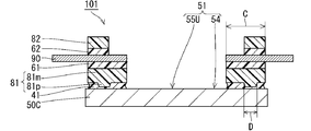
- the package 101 includes the external terminal electrode 90 attached to the frame body 81 and the exposed surface of the frame body 81.
- the lid 300 may be attached to the lid 300 via the adhesive layer 46 to seal the lid 300.
- At least one of alumina, aluminum hydroxide, talc, iron oxide, wollastonite, calcium carbonate, mica, titanium oxide, and carbon fiber is used in place of, or in combination with, at least one of silica glass and crystalline silica.
- the shape of the inorganic filler is, for example, spherical, fibrous, or plate-like.
- the content of the inorganic filler may be adjusted from the viewpoint of controlling the fluidity of the adhesive layer 41, and is preferably 1 wt% to 10 wt%. From the viewpoint of ensuring the fluidity of the adhesive layer 41 before curing, spherical silica glass (non-crystalline silica) having a particle size of 1 ⁇ m to 50 ⁇ m is optimal.
- the adhesive layer 41 (FIG. 4) preferably has a concave side surface that connects the heat sink plate 50C and the frame body 81. As a result, the effect of stress relaxation by the adhesive layer 41 can be enhanced.
- the power semiconductor element 200 is mounted on the heat sink plate 50C after the package 101 (FIG. 4) is formed. Therefore, the power semiconductor element 200 is mounted on the heat sink plate 50C after the adhesive layer 41 for adhering the frame body 81 and the heat sink plate 50C to each other is formed. Since heating is required for this mounting, the temperature of the adhesive layer 41 also rises. Therefore, if the adhesive layer 41 does not have a sufficiently thick portion, the stress caused by the difference in thermal expansion between the frame body 81 and the heat sink plate 50C is relaxed by the adhesive layer 41. Is likely to be low.
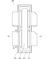
- FIG. 11 is a partial cross-sectional view schematically showing the configuration of the package 103 according to the third embodiment.
- the package 103 has a frame body 81 and a heat sink plate 50, both of which are members having a protrusion and a flat portion.
- the protrusion S1p of the frame body 81 and the protrusion S2p of the heat sink plate 50 are substantially entirely overlapped.
- Package 106 has an insertion member 88.
- the insertion member 88 is arranged inside the adhesive layer 41. In the plane layout, the area of the insertion member 88 is smaller than the area of the frame body 81C.
- the material of the insertion member 88 is not particularly limited, and the insertion member 88 may be made of, for example, a metal, a resin, or a resin in which an inorganic filler is dispersed. This resin is preferably a thermosetting resin from the viewpoint of productivity of the insertion member 88. Thermosetting resins are suitable for manufacturing processes such as injection molding.
- the resistance to the gloss leak test was improved in proportion to the thickness A.
- the paste is applied a plurality of times in order to form the adhesive layer 41 having a large thickness A, which is a heavy burden on the process.
- the thickness A, thickness B, width C, width D, length E, interval F, and height G in Table 2 above are the dimensions shown in FIGS. 4 to 6.
- the material of each member was the same as that of the corresponding member in the above comparative example.
Landscapes
- Cooling Or The Like Of Semiconductors Or Solid State Devices (AREA)
Priority Applications (2)
| Application Number | Priority Date | Filing Date | Title |
|---|---|---|---|
| JP2021527413A JP7290723B2 (ja) | 2019-06-25 | 2020-04-20 | パッケージ、および、パワー半導体モジュールの製造方法 |
| US17/455,709 US11901268B2 (en) | 2019-06-25 | 2021-11-19 | Package with an electrode-attached frame supported by a heat sink, and method for manufacturing power semiconductor module provided therewith |
Applications Claiming Priority (2)
| Application Number | Priority Date | Filing Date | Title |
|---|---|---|---|
| JP2019-117393 | 2019-06-25 | ||
| JP2019117393 | 2019-06-25 |
Related Child Applications (1)
| Application Number | Title | Priority Date | Filing Date |
|---|---|---|---|
| US17/455,709 Continuation US11901268B2 (en) | 2019-06-25 | 2021-11-19 | Package with an electrode-attached frame supported by a heat sink, and method for manufacturing power semiconductor module provided therewith |
Publications (1)
| Publication Number | Publication Date |
|---|---|
| WO2020261730A1 true WO2020261730A1 (ja) | 2020-12-30 |
Family
ID=74061352
Family Applications (1)
| Application Number | Title | Priority Date | Filing Date |
|---|---|---|---|
| PCT/JP2020/017028 Ceased WO2020261730A1 (ja) | 2019-06-25 | 2020-04-20 | パッケージ、および、パワー半導体モジュールの製造方法 |
Country Status (3)
| Country | Link |
|---|---|
| US (1) | US11901268B2 (https=) |
| JP (1) | JP7290723B2 (https=) |
| WO (1) | WO2020261730A1 (https=) |
Cited By (1)
| Publication number | Priority date | Publication date | Assignee | Title |
|---|---|---|---|---|
| US12477704B2 (en) | 2021-01-22 | 2025-11-18 | Mitsubishi Electric Corporation | Power semiconductor device and method of manufacturing the same, and power conversion device |
Families Citing this family (2)
| Publication number | Priority date | Publication date | Assignee | Title |
|---|---|---|---|---|
| EP3796373B1 (de) * | 2019-09-20 | 2023-06-28 | BIOTRONIK SE & Co. KG | Platinenanordnung eines implantierbaren medizinischen geräts |
| JP7444814B2 (ja) * | 2021-04-27 | 2024-03-06 | Ngkエレクトロデバイス株式会社 | パッケージ |
Citations (6)
| Publication number | Priority date | Publication date | Assignee | Title |
|---|---|---|---|---|
| JP2005322697A (ja) * | 2004-05-06 | 2005-11-17 | Denso Corp | 電子制御装置 |
| US20070090514A1 (en) * | 2005-10-24 | 2007-04-26 | Freescale Semiconductor, Inc. | Semiconductor structure and method of manufacture |
| JP2007165486A (ja) * | 2005-12-12 | 2007-06-28 | Shinko Electric Ind Co Ltd | 放熱板及び半導体装置 |
| JP2009513026A (ja) * | 2005-10-24 | 2009-03-26 | フリースケール セミコンダクター インコーポレイテッド | 半導体構造及び組み立て方法 |
| JP2018142617A (ja) * | 2017-02-28 | 2018-09-13 | 三菱電機株式会社 | 半導体装置およびその製造方法 |
| WO2018225511A1 (ja) * | 2017-06-08 | 2018-12-13 | Ngkエレクトロデバイス株式会社 | 蓋体、電子装置の製造方法および電子装置 |
Family Cites Families (5)
| Publication number | Priority date | Publication date | Assignee | Title |
|---|---|---|---|---|
| JP2003068919A (ja) * | 2001-08-27 | 2003-03-07 | Nec Yamagata Ltd | 半導体装置 |
| JP3816821B2 (ja) | 2002-03-20 | 2006-08-30 | 株式会社住友金属エレクトロデバイス | 高周波用パワーモジュール基板及びその製造方法 |
| JP2004179584A (ja) | 2002-11-29 | 2004-06-24 | Toyo Jushi Kk | トランジスタパッケージ及びその製造方法 |
| JP2005150133A (ja) | 2003-11-11 | 2005-06-09 | Sumitomo Metal Electronics Devices Inc | 半導体素子収納用容器 |
| JP2012049224A (ja) | 2010-08-25 | 2012-03-08 | Kyocera Corp | 実装構造体および実装構造体の製造方法 |
-
2020
- 2020-04-20 WO PCT/JP2020/017028 patent/WO2020261730A1/ja not_active Ceased
- 2020-04-20 JP JP2021527413A patent/JP7290723B2/ja active Active
-
2021
- 2021-11-19 US US17/455,709 patent/US11901268B2/en active Active
Patent Citations (6)
| Publication number | Priority date | Publication date | Assignee | Title |
|---|---|---|---|---|
| JP2005322697A (ja) * | 2004-05-06 | 2005-11-17 | Denso Corp | 電子制御装置 |
| US20070090514A1 (en) * | 2005-10-24 | 2007-04-26 | Freescale Semiconductor, Inc. | Semiconductor structure and method of manufacture |
| JP2009513026A (ja) * | 2005-10-24 | 2009-03-26 | フリースケール セミコンダクター インコーポレイテッド | 半導体構造及び組み立て方法 |
| JP2007165486A (ja) * | 2005-12-12 | 2007-06-28 | Shinko Electric Ind Co Ltd | 放熱板及び半導体装置 |
| JP2018142617A (ja) * | 2017-02-28 | 2018-09-13 | 三菱電機株式会社 | 半導体装置およびその製造方法 |
| WO2018225511A1 (ja) * | 2017-06-08 | 2018-12-13 | Ngkエレクトロデバイス株式会社 | 蓋体、電子装置の製造方法および電子装置 |
Cited By (1)
| Publication number | Priority date | Publication date | Assignee | Title |
|---|---|---|---|---|
| US12477704B2 (en) | 2021-01-22 | 2025-11-18 | Mitsubishi Electric Corporation | Power semiconductor device and method of manufacturing the same, and power conversion device |
Also Published As
| Publication number | Publication date |
|---|---|
| JPWO2020261730A1 (https=) | 2020-12-30 |
| JP7290723B2 (ja) | 2023-06-13 |
| US11901268B2 (en) | 2024-02-13 |
| US20220077033A1 (en) | 2022-03-10 |
Similar Documents
| Publication | Publication Date | Title |
|---|---|---|
| TWI415228B (zh) | 半導體封裝結構、覆晶封裝、及半導體覆晶封裝的形成方法 | |
| CN101335263B (zh) | 半导体模块和半导体模块的制造方法 | |
| CN105405815B (zh) | 半导体装置及其制造方法 | |
| CN107112316B (zh) | 半导体模块 | |
| JP5570476B2 (ja) | 半導体装置および半導体装置の製造方法 | |
| US9082707B2 (en) | Semiconductor device and method for manufacturing semiconductor device | |
| JP5807348B2 (ja) | 半導体装置およびその製造方法 | |
| WO2020261730A1 (ja) | パッケージ、および、パワー半導体モジュールの製造方法 | |
| CN1390088A (zh) | 电力组件及其制造方法 | |
| CN113451219B (zh) | 在与安装基座的模块接口处具有气流抑制密封部的模块 | |
| CN108604589B (zh) | 半导体装置及其制造方法 | |
| JP7439521B2 (ja) | 半導体モジュール及び半導体モジュールの製造方法 | |
| JP7543703B2 (ja) | 半導体装置 | |
| US11978682B2 (en) | Package, and method for manufacturing power semiconductor module | |
| JP2016111083A (ja) | パワーモジュール及びその製造方法 | |
| JP2020155699A (ja) | パッケージ、および、パワー半導体モジュールの製造方法 | |
| JP7159464B2 (ja) | パワー半導体モジュールおよびその製造方法 | |
| JP7072624B1 (ja) | 電力用半導体装置および電力用半導体装置の製造方法 | |
| JP2023114084A (ja) | 半導体装置及び半導体装置の製造方法 | |
| JP2021150421A (ja) | パッケージ | |
| JP2023132461A (ja) | パッケージ | |
| WO2021171881A1 (ja) | パッケージ | |
| US20250285937A1 (en) | Housing, semiconductor module comprising a housing, and method for assembling a semiconductor module | |
| JP2023077604A (ja) | パッケージ | |
| WO2023073831A1 (ja) | 半導体装置及び半導体装置の製造方法 |
Legal Events
| Date | Code | Title | Description |
|---|---|---|---|
| 121 | Ep: the epo has been informed by wipo that ep was designated in this application |
Ref document number: 20833246 Country of ref document: EP Kind code of ref document: A1 |
|
| ENP | Entry into the national phase |
Ref document number: 2021527413 Country of ref document: JP Kind code of ref document: A |
|
| NENP | Non-entry into the national phase |
Ref country code: DE |
|
| 122 | Ep: pct application non-entry in european phase |
Ref document number: 20833246 Country of ref document: EP Kind code of ref document: A1 |