WO2020255666A1 - 基板構造体 - Google Patents
基板構造体 Download PDFInfo
- Publication number
- WO2020255666A1 WO2020255666A1 PCT/JP2020/021110 JP2020021110W WO2020255666A1 WO 2020255666 A1 WO2020255666 A1 WO 2020255666A1 JP 2020021110 W JP2020021110 W JP 2020021110W WO 2020255666 A1 WO2020255666 A1 WO 2020255666A1
- Authority
- WO
- WIPO (PCT)
- Prior art keywords
- conductive plate
- sheet
- base substrate
- wiring member
- terminal
- Prior art date
- Legal status (The legal status is an assumption and is not a legal conclusion. Google has not performed a legal analysis and makes no representation as to the accuracy of the status listed.)
- Ceased
Links
Images


Classifications
-
- H—ELECTRICITY
- H05—ELECTRIC TECHNIQUES NOT OTHERWISE PROVIDED FOR
- H05K—PRINTED CIRCUITS; CASINGS OR CONSTRUCTIONAL DETAILS OF ELECTRIC APPARATUS; MANUFACTURE OF ASSEMBLAGES OF ELECTRICAL COMPONENTS
- H05K1/00—Printed circuits
- H05K1/02—Details
- H05K1/0201—Thermal arrangements, e.g. for cooling, heating or preventing overheating
- H05K1/0203—Cooling of mounted components
- H05K1/0207—Cooling of mounted components using internal conductor planes parallel to the surface for thermal conduction, e.g. power planes
-
- H—ELECTRICITY
- H05—ELECTRIC TECHNIQUES NOT OTHERWISE PROVIDED FOR
- H05K—PRINTED CIRCUITS; CASINGS OR CONSTRUCTIONAL DETAILS OF ELECTRIC APPARATUS; MANUFACTURE OF ASSEMBLAGES OF ELECTRICAL COMPONENTS
- H05K1/00—Printed circuits
- H05K1/18—Printed circuits structurally associated with non-printed electric components
- H05K1/181—Printed circuits structurally associated with non-printed electric components associated with surface mounted components
-
- H—ELECTRICITY
- H05—ELECTRIC TECHNIQUES NOT OTHERWISE PROVIDED FOR
- H05K—PRINTED CIRCUITS; CASINGS OR CONSTRUCTIONAL DETAILS OF ELECTRIC APPARATUS; MANUFACTURE OF ASSEMBLAGES OF ELECTRICAL COMPONENTS
- H05K1/00—Printed circuits
- H05K1/02—Details
- H05K1/0201—Thermal arrangements, e.g. for cooling, heating or preventing overheating
- H05K1/0203—Cooling of mounted components
- H05K1/0209—External configuration of printed circuit board adapted for heat dissipation, e.g. lay-out of conductors, coatings
-
- H—ELECTRICITY
- H05—ELECTRIC TECHNIQUES NOT OTHERWISE PROVIDED FOR
- H05K—PRINTED CIRCUITS; CASINGS OR CONSTRUCTIONAL DETAILS OF ELECTRIC APPARATUS; MANUFACTURE OF ASSEMBLAGES OF ELECTRICAL COMPONENTS
- H05K1/00—Printed circuits
- H05K1/02—Details
- H05K1/0213—Electrical arrangements not otherwise provided for
- H05K1/0263—High current adaptations, e.g. printed high current conductors or using auxiliary non-printed means; Fine and coarse circuit patterns on one circuit board
-
- H—ELECTRICITY
- H05—ELECTRIC TECHNIQUES NOT OTHERWISE PROVIDED FOR
- H05K—PRINTED CIRCUITS; CASINGS OR CONSTRUCTIONAL DETAILS OF ELECTRIC APPARATUS; MANUFACTURE OF ASSEMBLAGES OF ELECTRICAL COMPONENTS
- H05K1/00—Printed circuits
- H05K1/02—Details
- H05K1/09—Use of materials for the conductive, e.g. metallic pattern
-
- H—ELECTRICITY
- H05—ELECTRIC TECHNIQUES NOT OTHERWISE PROVIDED FOR
- H05K—PRINTED CIRCUITS; CASINGS OR CONSTRUCTIONAL DETAILS OF ELECTRIC APPARATUS; MANUFACTURE OF ASSEMBLAGES OF ELECTRICAL COMPONENTS
- H05K2201/00—Indexing scheme relating to printed circuits covered by H05K1/00
- H05K2201/10—Details of components or other objects attached to or integrated in a printed circuit board
- H05K2201/10007—Types of components
- H05K2201/10166—Transistor
-
- H—ELECTRICITY
- H05—ELECTRIC TECHNIQUES NOT OTHERWISE PROVIDED FOR
- H05K—PRINTED CIRCUITS; CASINGS OR CONSTRUCTIONAL DETAILS OF ELECTRIC APPARATUS; MANUFACTURE OF ASSEMBLAGES OF ELECTRICAL COMPONENTS
- H05K2201/00—Indexing scheme relating to printed circuits covered by H05K1/00
- H05K2201/10—Details of components or other objects attached to or integrated in a printed circuit board
- H05K2201/10227—Other objects, e.g. metallic pieces
- H05K2201/10272—Busbars, i.e. thick metal bars mounted on the printed circuit board [PCB] as high-current conductors
-
- H—ELECTRICITY
- H05—ELECTRIC TECHNIQUES NOT OTHERWISE PROVIDED FOR
- H05K—PRINTED CIRCUITS; CASINGS OR CONSTRUCTIONAL DETAILS OF ELECTRIC APPARATUS; MANUFACTURE OF ASSEMBLAGES OF ELECTRICAL COMPONENTS
- H05K2201/00—Indexing scheme relating to printed circuits covered by H05K1/00
- H05K2201/10—Details of components or other objects attached to or integrated in a printed circuit board
- H05K2201/10431—Details of mounted components
- H05K2201/10507—Involving several components
- H05K2201/10522—Adjacent components
-
- H—ELECTRICITY
- H05—ELECTRIC TECHNIQUES NOT OTHERWISE PROVIDED FOR
- H05K—PRINTED CIRCUITS; CASINGS OR CONSTRUCTIONAL DETAILS OF ELECTRIC APPARATUS; MANUFACTURE OF ASSEMBLAGES OF ELECTRICAL COMPONENTS
- H05K2201/00—Indexing scheme relating to printed circuits covered by H05K1/00
- H05K2201/10—Details of components or other objects attached to or integrated in a printed circuit board
- H05K2201/10431—Details of mounted components
- H05K2201/10507—Involving several components
- H05K2201/10545—Related components mounted on both sides of the PCB
-
- H—ELECTRICITY
- H05—ELECTRIC TECHNIQUES NOT OTHERWISE PROVIDED FOR
- H05K—PRINTED CIRCUITS; CASINGS OR CONSTRUCTIONAL DETAILS OF ELECTRIC APPARATUS; MANUFACTURE OF ASSEMBLAGES OF ELECTRICAL COMPONENTS
- H05K2201/00—Indexing scheme relating to printed circuits covered by H05K1/00
- H05K2201/10—Details of components or other objects attached to or integrated in a printed circuit board
- H05K2201/10431—Details of mounted components
- H05K2201/10553—Component over metal, i.e. metal plate in between bottom of component and surface of PCB
-
- H—ELECTRICITY
- H05—ELECTRIC TECHNIQUES NOT OTHERWISE PROVIDED FOR
- H05K—PRINTED CIRCUITS; CASINGS OR CONSTRUCTIONAL DETAILS OF ELECTRIC APPARATUS; MANUFACTURE OF ASSEMBLAGES OF ELECTRICAL COMPONENTS
- H05K2201/00—Indexing scheme relating to printed circuits covered by H05K1/00
- H05K2201/10—Details of components or other objects attached to or integrated in a printed circuit board
- H05K2201/10613—Details of electrical connections of non-printed components, e.g. special leads
- H05K2201/10621—Components characterised by their electrical contacts
- H05K2201/10681—Tape Carrier Package [TCP]; Flexible sheet connector
-
- H—ELECTRICITY
- H05—ELECTRIC TECHNIQUES NOT OTHERWISE PROVIDED FOR
- H05K—PRINTED CIRCUITS; CASINGS OR CONSTRUCTIONAL DETAILS OF ELECTRIC APPARATUS; MANUFACTURE OF ASSEMBLAGES OF ELECTRICAL COMPONENTS
- H05K2201/00—Indexing scheme relating to printed circuits covered by H05K1/00
- H05K2201/10—Details of components or other objects attached to or integrated in a printed circuit board
- H05K2201/10613—Details of electrical connections of non-printed components, e.g. special leads
- H05K2201/10954—Other details of electrical connections
- H05K2201/10977—Encapsulated connections
-
- H—ELECTRICITY
- H05—ELECTRIC TECHNIQUES NOT OTHERWISE PROVIDED FOR
- H05K—PRINTED CIRCUITS; CASINGS OR CONSTRUCTIONAL DETAILS OF ELECTRIC APPARATUS; MANUFACTURE OF ASSEMBLAGES OF ELECTRICAL COMPONENTS
- H05K2201/00—Indexing scheme relating to printed circuits covered by H05K1/00
- H05K2201/10—Details of components or other objects attached to or integrated in a printed circuit board
- H05K2201/10613—Details of electrical connections of non-printed components, e.g. special leads
- H05K2201/10954—Other details of electrical connections
- H05K2201/10984—Component carrying a connection agent, e.g. solder, adhesive
Definitions
- This disclosure relates to a substrate structure.
- Patent Document 1 discloses a circuit configuration including a plurality of bus bars, a semiconductor switching element, and a control circuit board.
- the bus bars are adhered to the surface of the control circuit board while being lined up on substantially the same plane.
- Semiconductor switching elements are mounted on both the bus bar and the control circuit board.
- Patent Document 2 discloses an electric junction box provided with a pair of bus bars and a blocking unit mounted on the pair of bus bars to energize and shut off the pair of bus bars.
- Patent Documents 1 and 2 a plurality of semiconductor switching elements are mounted on one main surface side of a bus bar arranged in the same plane. Here, it is required to further reduce the size of the substrate structure including the bus bar and a plurality of elements connected to the bus bar.
- the purpose of the present disclosure is to further reduce the size of the substrate structure including a plurality of elements.
- the substrate structure of the present disclosure includes a base substrate including a first conductive plate and a second conductive plate, a first element connected to the first conductive plate and the second conductive plate, the first conductive plate, and the first conductive plate.
- a second element connected to the second conductive plate is provided, and the first conductive plate and the second conductive plate are arranged along the same plane in a state of being insulated from each other in the base substrate.
- the first element is mounted on the first main surface of the base substrate, and the second element is mounted on the second main surface of the base substrate opposite to the first main surface. It is a substrate structure.
- a substrate structure including a plurality of elements can be further miniaturized.
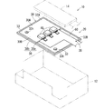
- FIG. 1 is a schematic exploded perspective view showing an electrical connection box according to the first embodiment.
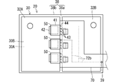
- FIG. 2 is a plan view showing the substrate structure.
- FIG. 3 is a bottom view showing the substrate structure.
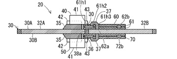
- FIG. 4 is a sectional view taken along line IV-IV of FIG.
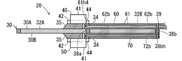
- FIG. 5 is a sectional view taken along line VV of FIG.
- FIG. 6 is a plan view showing the substrate structure according to the second embodiment.
- FIG. 7 is a bottom view showing the substrate structure.
- FIG. 8 is a plan view showing a substrate structure according to a modified example of the second embodiment.
- the substrate structure of the present disclosure is as follows.
- a base substrate including a first conductive plate and a second conductive plate, a first element connected to the first conductive plate and the second conductive plate, the first conductive plate and the second conductive plate.
- the first conductive plate and the second conductive plate are arranged along the same plane in a state of being insulated from each other, and the first conductive plate is provided with a second element connected to the first conductive plate.
- the first element and the second element may be arranged in a small region so as not to interfere with each other. Therefore, the substrate structure including the plurality of elements can be further miniaturized.
- the base substrate includes an insulating portion formed by molding the first conductive plate and the second conductive plate as inserts, and the insulating portion includes the first conductive plate and the second conductive plate.
- the first conductive plate and the second conductive plate may be kept in a state along the same plane while insulating the space between them.
- the first conductive plate and the second conductive plate are held in a state of being insulated by the insulating portion, and the first conductive plate and the second conductive plate are held along the same plane.
- the first element and the second element may be mounted so as to at least partially overlap each other in the direction along the boundary between the first conductive plate and the second conductive plate.
- the first element and the second element can be arranged in a region as small as possible.
- the first element and the second element may be dispersedly mounted on both sides of the boundary between the first conductive plate and the second conductive plate.
- the heat generated by the first element and the second element is dispersed. As a result, the heat dissipation effect is enhanced.
- a first sheet-shaped wiring member superposed on the first main surface of the base substrate and a second sheet-shaped wiring member superposed on the second main surface of the base substrate are further provided.
- the first element includes a first control terminal into which a control signal is input, and energizes and shuts off between the first conductive plate and the second conductive plate in response to a control signal to the first control terminal.
- the second element includes a second control terminal into which a control signal is input, and the first conductive plate and the second conductive plate in response to a control signal to the second control terminal. It is a second switching element that energizes and shuts off from the plate, and the first sheet-shaped wiring member includes a first linear conductor connected to the first control terminal, and the second sheet-shaped wiring member. May include a second linear conductor connected to the second control terminal.
- the first control terminal and the second control terminal can be connected to the outside by using the first sheet-shaped wiring member or the second sheet-shaped wiring member.
- the first linear conductor and the second linear conductor are electrically connected via a conductive portion in a portion of the base substrate other than the first conductive plate and the second conductive plate. May be good.
- the first control terminal and the second control terminal are easily connected to an external control board.
- the substrate structure according to the first embodiment will be described.
- the electrical junction box 10 including the substrate structure 20 will be described as an example.
- FIG. 1 is a schematic exploded perspective view showing the electrical connection box 10 according to the first embodiment.
- FIG. 2 is a plan view showing the substrate structure 20.
- FIG. 3 is a bottom view showing the substrate structure 20.
- FIG. 4 is a sectional view taken along line IV-IV of FIG.
- FIG. 5 is a sectional view taken along line VV of FIG.
- the thickness and the like of each part may be exaggerated in FIGS. 4 and 5.
- the electrical junction box 10 includes a substrate structure 20, a housing 12, and a control substrate 14.
- the housing 12 is made of resin or the like.
- the substrate structure 20 and the control substrate 14 are housed in the housing 12.
- the housing 12 is formed with a recess for exposing the external connection portion 33 of the substrate structure 20 to the outside.
- the substrate structure 20 includes a base substrate 30, a first element 40, and a second element 50.
- the base substrate 30 includes a first conductive plate 32A and a second conductive plate 32B.
- the first element 40 is connected to the first conductive plate 32A and the second conductive plate 32B.
- the second element 50 is connected to the first conductive plate 32A and the second conductive plate 32B.
- the current flows through the first conductive plate 32A, the first element 40, the second element 50, and the second conductive plate 32B.
- the direction in which the current flows may be any of the first conductive plate 32A to the second conductive plate 32B and the second conductive plate 32B to the first conductive plate 32A.
- the control board 14 is connected to the board structure 20.
- the control board 14 controls the operation of the board structure 20.
- the control board 14 controls on / off of the current flowing through the board structure 20.
- the electric junction box 10 is provided, for example, in a power supply path between a power source and various electrical components in an automobile.
- the substrate structure 20 includes a base substrate 30, a first element 40, and a second element 50.
- the base substrate 30 includes a first conductive plate 32A and a second conductive plate 32B.
- the first conductive plate 32A and the second conductive plate 32B are members formed of a metal plate or the like.
- the first conductive plate 32A and the second conductive plate 32B are sometimes called a bus bar.
- the first conductive plate 32A and the second conductive plate 32B are formed in a square plate shape.
- the first conductive plate 32A and the second conductive plate 32B function as an external path for the current flowing through the first element 40 and the second element 50.
- the first conductive plate 32A and the second conductive plate 32B are arranged along the same plane in a state of being insulated from each other.
- a straight edge portion is formed on a part of the outer periphery of the first conductive plate 32A.
- a straight edge portion is formed on a part of the outer periphery of the second conductive plate 32B.
- the straight edge portion of the first conductive plate 32A and the straight edge portion of the second conductive plate 32B are parallel to each other and face each other with a gap. Therefore, the first conductive plate 32A and the second conductive plate 32B are in a state of being insulated from each other.
- the base substrate 30 further includes an insulating portion 38.
- the insulating portion 38 is a portion formed of resin or the like.
- the insulating portion 38 is a portion formed by using the first conductive plate 32A and the second conductive plate 32B as inserts.
- the insulating portion 38 includes an insulating interposing portion 38a and an insulating holding portion 38b.
- the insulating intervening portion 38a is provided between the straight edge portion of the first conductive plate 32A and the straight edge portion of the second conductive plate 32B.
- the insulating intervening portion 38a keeps the first conductive plate 32A and the second conductive plate 32B in a state of being insulated as reliably as possible.
- the insulation holding portion 38b is provided so as to surround the outer periphery of the first conductive plate 32A and the second conductive plate 32B.
- the first conductive plate 32A and the second conductive plate 32B are surrounded by the insulating interposing portion 38a and the insulating holding portion 38b, so that the first conductive plate 32A and the second conductive plate 32B are held along the same plane. ..
- the first conductive plate 32A and the second conductive plate 32B may be kept in a state of being arranged along the same plane in a state of being insulated from each other by another configuration.
- the first conductive plate 32A and the second conductive plate 32B may be fitted into a resin frame member that has been molded in advance.
- the first conductive plate 32A and the second conductive plate 32B may be joined to a sheet-shaped member or the like. In this case, it is sufficient that a hole is formed in a portion of the sheet-shaped member on which the element is mounted.
- Holes 33h are formed in the first conductive plate 32A and the second conductive plate 32B.
- the portion of the first conductive plate 32A and the second conductive plate 32B in which the hole 33h is formed functions as an external connecting portion 33 for connecting the first conductive plate 32A and the second conductive plate 32B to an external conductive path. can do.
- the first element 40 is an element connected to the first conductive plate 32A and the second conductive plate 32B.
- the first element 40 is an element according to the application of the electrical junction box 10.
- a semiconductor switching element exemplified by a field effect transistor (hereinafter, also referred to as “FET”) is adopted.
- the first element 40 may be a resistor, a coil, or a capacitor.
- the first element 40 is an FET. More specifically, the first element 40 is, for example, a surface mount type power MOSFET.
- the first element 40 includes an element main body 41, a first terminal 42, a second terminal 43, and a third terminal 44.
- One of the first terminal 42 and the second terminal 43 functions as a source electrode, and the other functions as a drain electrode.
- the first terminal 42 is the drain electrode and the second terminal 43 is the source electrode.
- the third terminal 44 is, for example, a first control terminal into which a control signal is input.
- the first element 40 energizes and shuts off between the first conductive plate 32A and the second conductive plate 32B.
- the third terminal 44 is a gate electrode.
- the element body 41 is formed, for example, in a flat rectangular parallelepiped shape.
- the first terminal 42 is provided so as to project from the bottom of the element main body 41 to one side.
- the second terminal 43 and the third terminal 44 are provided so as to project from the other side of the element main body 41.
- a plurality of second terminals 43 are provided.
- the first element 40 is connected to the first conductive plate 32A and the second conductive plate 32B. Further, the first element 40 is mounted on the first main surface 30A of the base substrate 30. In the present embodiment, the element main body 41 of the first element 40 is located on the first conductive plate 32A.
- the first terminal 42 is electrically connected to the first conductive plate 32A on the first conductive plate 32A.
- the first terminal 42 is connected to the first conductive plate 32A by the solder 35 (see FIG. 4).
- the solder connection points of the two parts may be fixed in a state where the two parts are electrically connected. For example, the two parts may be connected by a conductive adhesive.
- the second terminal 43 is connected to the second conductive plate 32B.
- the second terminal 43 extends from the element main body 41 on the first conductive plate 32A to the second conductive plate 32B side.
- the second terminal 43 is located on the insulating interposition portion 38a.
- the second terminal 43 is electrically connected to the second conductive plate 32B via the first sheet-shaped wiring member 60.
- the first sheet-shaped wiring member 60 is a member in which the conductor is covered with an insulating member and formed in a sheet shape.
- the first sheet-shaped wiring member 60 is a flexible printed circuit board (FPC) is exemplified. That is, the first sheet-shaped wiring member 60 is a sheet-shaped member in which a conductor formed of a metal foil (copper foil) or the like is sandwiched between a pair of resin films 61.
- the first sheet-shaped wiring member 60 is formed in a sheet shape extending from the insulating interposing portion 38a toward the second conductive plate 32B on the first main surface of the base substrate 30.
- the first sheet-shaped wiring member 60 includes a relay conductor 62a and a first linear conductor 62b as conductors.
- the relay conductor 62a is formed so as to extend from the lower region of the second terminal 43 of the first element 40 toward the second conductive plate 32B.
- the relay conductor 62a is formed in a rectangular region extending from a region extending downwardly of the plurality of second terminals 43 toward the second conductive plate 32B.
- the resin film 61 on the side of the second terminal 43 is formed with an opening 61h1 that opens in a region directly below the second terminal 43.
- the resin film 61 on the side of the second terminal 43 is formed with an opening 61h2 that opens in a region closer to the second conductive plate 32B than the opening 61h1.
- the relay conductor 62a can be exposed.
- first sheet-shaped wiring member 60 is formed with a through hole 61h3 that penetrates in a region away from the opening 61h2.
- the second conductive plate 32B can be exposed in the through hole 61h3.
- the second terminal 43 is connected to the relay conductor 62a exposed by the opening 61h1 by the solder 36 in a state where the first sheet-shaped wiring member 60 is superposed on the first main surface 30A of the base substrate 30 (FIG. 4). reference). Further, the relay conductor 62a exposed by the opening 61h2 and the second conductive plate 32B exposed by the through hole 61h3 are connected by the solder 37 (see FIG. 4). Therefore, the second terminal 43 is electrically connected to the second conductive plate 32B via the solder 36, the relay conductor 62a, and the solder 37. Therefore, the first element 40 is mounted on the first main surface 30A of the base substrate 30 in a state of being connected to the first conductive plate 32A and the second conductive plate 32B. The second terminal 43 may be directly connected to the second conductive plate 32B by solder or the like.
- the third terminal 44 is connected to the first linear conductor 62b.
- the first linear conductor 62b is a linear conductor extending from the lower region of the third terminal 44 toward any part of the outer circumference of the base substrate 30.
- the resin film 61 on the third terminal 44 side is formed with an opening 61h4 that opens in a region directly below the third terminal 44.
- the third terminal 44 is connected to the first linear conductor 62b exposed by the opening 61h4 by a solder 34 (see FIG. 5).
- the first sheet-shaped wiring member 60 may extend outward from the base board 30 and be connected to the control board 14.
- the first linear conductor 62b may extend outward of the first sheet-shaped wiring member 60 and be connected to the control board 14.
- the control signal output from the control board 14 is given to the third terminal 44 via the first linear conductor 62b.
- the second element 50 has the same configuration as the first element 40. Each part of the second element 50 is designated by the same reference numeral as that of the first element 40, and redundant description is omitted.
- the second element 50 is connected to the first conductive plate 32A and the second conductive plate 32B. Further, the second element 50 is mounted on the second main surface 30B of the base substrate 30.
- the configuration for mounting the second element 50 on the base substrate 30 is the same as the configuration for mounting the first element 40 on the base substrate 30, except for the following configuration. The difference is that the second element 50 is mounted on the second main surface 30B on the side opposite to the first main surface 30A with respect to the base substrate 30, and the second element 50 is replaced with the first sheet-shaped wiring member 60. The point is that the sheet-shaped wiring member 70 is used.
- the side opposite to the first main surface 30A with respect to the base substrate 30 means the side opposite to the thickness direction of the base substrate 30.
- the configuration for mounting the second element 50 on the base substrate 30 the same components as the configuration for mounting the first element 40 on the base substrate 30 are designated by the same reference numerals, and redundant description is omitted. Will be done.
- the position where the second element 50 is mounted is a region opposite to the region where the first element 40 is mounted in the thickness direction of the base substrate 30. Therefore, when the substrate structure 20 is viewed in a plane in a direction along the thickness direction thereof, the first element 40 and the second element 50 are arranged in a region where they overlap each other.
- first element 40 and the second element 50 are arranged in the same region in a plan view of the substrate structure 20. Even if the first element 40 and the second element 50 are mounted at positions displaced from each other in the direction along the boundary between the first conductive plate 32A and the second conductive plate 32B (here, the insulating interposition portion 38a). Good. In this case, the first element 40 and the second element 50 partially overlap each other in the direction along the boundary between the first conductive plate 32A and the second conductive plate 32B (here, the insulating interposition portion 38a). It is preferable to have.
- first element 40 and the second element 50 may be mounted on the first conductive plate 32A side, and the other may be mounted on the second conductive plate 32B side. Also in this case, it is preferable that the first element 40 and the second element 50 are mounted so as to at least partially overlap each other in the direction along the boundary between the first conductive plate 32A and the second conductive plate 32B. .. An example of the latter will be described in Embodiment 2.
- the second sheet-shaped wiring member 70 differs from the first sheet-shaped wiring member 60 in the following points.
- the second sheet-shaped wiring member 70 is superposed on the second main surface 30B on the side opposite to the first main surface 30A with respect to the base substrate 30.
- a portion of the first sheet-shaped wiring member 60 that extends outward from the base substrate 30 and is connected to the control substrate 14 is omitted.
- the second linear conductor 72b corresponding to the first linear conductor 62b is connected to the third terminal 44 of the second element 50.
- the second linear conductor 72b extends from the connection portion with respect to the third terminal 44 and reaches the insulation holding portion 38b.
- the third terminal of the second element 50 is an example of the second control terminal.
- the same components as those of the first sheet-shaped wiring member 60 are designated by the same reference numerals, and duplicate explanations are omitted.
- the first linear conductor 62b and the second linear conductor 72b are electrically connected via the conductive portion 39 in the portion of the base substrate 30 other than the first conductive plate 32A and the second conductive plate 32B.
- the first linear conductor 62b and the second linear conductor 72b extend along the same path.
- a portion of the first linear conductor 62b that passes through the insulation holding portion 38b and a portion of the second linear conductor 72b that reaches the insulation holding portion 38b are connected via a conductive portion 39.
- the conductive portion 39 is a conductive member that penetrates the insulation holding portion 38b and connects the first linear conductor 62b and the second linear conductor 72b.
- a through hole 38bh is formed in the insulation holding portion 38b. Further, a through hole is formed in a portion of the first linear conductor 62b and the second linear conductor 72b corresponding to the through hole 38bh, and the first linear conductor 62b and the second linear conductor are formed on the peripheral edge thereof.
- the conductor 72b is formed so as to be exposed. Then, solder is provided so as to penetrate the through hole 38bh on the inner peripheral surface or the entire inside of the through hole 38bh, and is soldered to the exposed portion of the first linear conductor 62b and the second linear conductor 72b. ..
- the conductive portion 39 formed in this way penetrates the through hole 38bh and electrically connects the first linear conductor 62b and the second linear conductor 72b.
- the case where the first element 40 is a plurality and the second element 50 is a plurality is exemplified.
- the plurality of first elements 40 are mounted side by side along the boundary between the first conductive plate 32A and the second conductive plate 32B.
- the first linear conductor 62b branches and extends toward the third terminal 44 of each of the plurality of first elements 40.
- the plurality of second elements 50 are mounted side by side along the boundary between the first conductive plate 32A and the second conductive plate 32B.
- the second linear conductor 72b branches and extends toward the third terminal 44 of each of the plurality of first elements 40.
- the plurality of first elements 40 and the plurality of second elements 50 are all located on the first conductive plate 32A side and mounted on the base substrate 30. Further, the distance between the plurality of first elements 40 and the distance between the plurality of second elements 50 are also the same. When the base substrate 30 is viewed in a plan view, the plurality of first elements 40 and the plurality of second elements 50 are in a positional relationship in which they overlap each other in the same region.
- the number of the first element 40 and the second element 50 is arbitrary.
- the first element 40 is mounted on the first main surface 30A with respect to the base substrate 30, and the second element 50 is mounted on the second main surface 30B with respect to the base substrate 30. Is implemented in. Therefore, the first element 40 and the second element 50 can be mounted in a region as small as possible so as not to interfere with each other. Therefore, the substrate structure 20 including the plurality of elements 40 and 50 can be further miniaturized.
- a plurality of elements connecting the first conductive plate and the second conductive plate will be mounted along the boundary between the first conductive plate and the second conductive plate. Assuming that a plurality of elements are mounted only on one main surface of the base substrate, since the plurality of elements are lined up along the boundary, the mounting area of the plurality of elements becomes large. Therefore, it is preferable that the first element 40 and the second element 50 are mounted so as to overlap each other in the direction along the boundary between the first conductive plate 32A and the second conductive plate 32B. As a result, the mounting regions of the plurality of elements 40 and 50 become smaller in the direction along the boundary between the first conductive plate 32A and the second conductive plate 32B.
- the first element 40 does not need to overlap with respect to all the plurality of second elements 50 in the direction along the boundary.
- the first element 40 may overlap a part of the plurality of second elements 50 in the direction along the boundary.
- the second element 50 does not need to overlap with respect to all the plurality of first elements 40 in the direction along the boundary.
- the second element 50 may overlap a part of the plurality of first elements 40 in the direction along the boundary.
- another element that does not overlap in the direction along the boundary with respect to the element on the opposite side may be mounted on the first main surface 30A or the second main surface 30B of the base substrate 30.
- first sheet-shaped wiring member 60 is superposed on the first main surface 30A of the base substrate 30.
- the first linear conductor 62b of the first sheet-shaped wiring member 60 is connected to the third terminal 44, which is the first control terminal of the first element 40.
- the second sheet-shaped wiring member 70 is superposed on the second main surface 30B of the base substrate 30.
- the second linear conductor 72b of the second sheet-shaped wiring member 70 is connected to the third terminal 44, which is the second control terminal of the second element 50. Therefore, the elements 40 and 50 mounted on both sides of the base board 30 are connected to the external control board 14 and the like via the first sheet-shaped wiring member 60 and the second sheet-shaped wiring member 70.
- the first sheet-shaped wiring member 60 and the second sheet-shaped wiring member 70 are electrically connected via the conductive portion 39. Therefore, for example, the first sheet-shaped wiring member 60 may be pulled out of the base substrate 30 and connected to the control substrate 14.
- the third terminal 44 which is the first control terminal of the first element 40
- the third terminal 44 which is the second control terminal of the second element 50
- FIG. 6 is a plan view showing the substrate structure 120.
- FIG. 7 is a bottom view of the substrate structure 120 as viewed from the side opposite to FIG.
- the same reference numerals are given to the components as described in the substrate structure 20 in the first embodiment, and the description thereof is omitted.
- the first element 40 is mounted on the first conductive plate 32A side.
- the mounting configuration of the first element 40 on the base substrate 30 is the same as that of the first embodiment.
- the difference between the substrate structure 120 and the substrate structure 20 is the mounting position of the second element 50 and the configuration for mounting the second element 50.
- the second element 50 is mounted on the second conductive plate 32B side. More specifically, the element main body 41 of the second element 50 is located on the second conductive plate 32B side.
- the first element 40 is provided on the first main surface 30A side with respect to the base substrate 30, and the second element 50 is provided on the second main surface 30B side on the opposite side.
- the first terminal 42 is located closer to the first conductive plate 32A with respect to the element main body 41, and the second terminal 43 and the third terminal 44 are the element main body 41. It is located closer to the second conductive plate 32B.
- a second sheet-shaped wiring member 170 is provided on the second main surface 30B side with respect to the base substrate 30. Like the first sheet-shaped wiring member 60, the second sheet-shaped wiring member 170 is provided with a second linear conductor (corresponding to the first linear conductor) as a conductor. Then, the second element 50 is mounted on the second sheet-shaped wiring member 170 in a state where the second sheet-shaped wiring member 170 is superposed on the second main surface 30B side of the second conductive plate 32B. At this time, the second terminal 43 is soldered to the second conductive plate 32B through the through hole of the second sheet-shaped wiring member 170. Further, the third terminal 44 is soldered to the second linear conductor of the second sheet-shaped wiring member 170. A control signal is given to the third terminal 44 via the second linear conductor.
- a second linear conductor corresponding to the first linear conductor
- Both the first sheet-shaped wiring member 60 and the second sheet-shaped wiring member 170 may be pulled out with respect to the base substrate 30.
- the first linear conductor of the first sheet-shaped wiring member 60 and the second linear conductor of the second sheet-shaped wiring member 170 are connected at any position on the base substrate 30, and the first sheet-shaped wiring member 60 And one of the second sheet-shaped wiring member 170 may be pulled out with respect to the base substrate 30.
- the first terminal 42 of the second element 50 extends from the second conductive plate 32B toward the insulating interposition portion 38a. At least a part of the second sheet-shaped wiring member 170 extends from the first terminal 42 toward the first conductive plate 32A as an extending portion 171. A relay conductor similar to the relay conductor 62a is provided in the extending portion 171. Similar to connecting the second terminal 43 to the second conductive plate 32B in the first embodiment, the first terminal 42 is connected to the relay conductor by solder, and the relay conductor is soldered to the first conductive plate 32A. Connected by 135. As a result, the first terminal 42 is electrically connected to the first conductive plate 32A.
- the first element 40 is mounted on the first conductive plate 32A side
- the second element 50 is mounted on the second conductive plate 32B side. That is, the second embodiment is an example in which the first element 40 and the second element 50 are dispersed and mounted on both sides of the boundary between the first conductive plate 32A and the second conductive plate 32B.
- the same effects as those of the first embodiment can be obtained. Further, since the first element 40 and the second element 50 are dispersed on both sides of the boundary, the heat generated by the first element 40 and the second element 50 is dispersed. Therefore, heat is efficiently dissipated from the substrate structure 120.
- the heat radiating member 190 such as the heat radiating fin is provided only on one side of the substrate structure 120, heat radiating is efficiently performed.
- the heat radiating member 190 is provided on one surface side of the substrate structure 120 (the first main surface 30A side of the base substrate 30).
- FIGS. 6 and 7 an example of the arrangement region of the heat radiating member 190 is illustrated by a two-dot chain line.
- the heat radiating member 190 may be arranged in direct contact with or close to the first element 40 at the portion where the first element 40 is mounted. Therefore, the heat generated by the first element 40 is efficiently dissipated by the heat radiating member 190.
- the heat radiating member 190 may be directly in contact with or close to the base substrate 30 from the side opposite to the second element 50.
- the heat generated by the second element 50 is transferred to the heat radiating member 190 via the base substrate 30 (here, the second conductive plate 32B), and is efficiently radiated. Therefore, the heat generated by the first element 40 and the second element 50 can be efficiently dissipated through the heat radiating member 190.
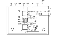
- FIG. 8 is a plan view showing the substrate structure 220 according to the modified example of the second embodiment.
- a plurality of (three in this case) first elements 40 are alternately mounted on the first conductive plate 32A side and the second conductive plate 32B side. That is, the plurality of first elements 40 are arranged so as to line up in the extending direction of the boundary between the first conductive plate 32A and the second conductive plate 32B.
- the odd-numbered first element 40 is mounted on the first conductive plate 32A side from one side to the other in the extending direction of the boundary.
- the even-numbered second element 50 is a second conductive plate. It is mounted on the 32B side.
- the configuration in which the odd-numbered first element 40 is mounted on the base substrate 30 and the configuration in which the first sheet-shaped wiring member 260 (corresponding to the first sheet-shaped wiring member 60) is connected are the same as in the first embodiment.
- the even-numbered first element 40 is mounted on the first sheet-shaped wiring member 260 on the base substrate 30 in the same posture as the odd-numbered first element 40.
- the second terminal 43 of the even-numbered first element 40 is soldered to the second conductive plate 32B through the through hole of the first sheet-shaped wiring member 260.
- the third terminal 44 of the even-numbered first element 40 is soldered to the first linear conductor 262b of the first sheet-shaped wiring member 260.
- the first terminal 42 of the even-numbered first element 40 extends from the second conductive plate 32B toward the insulating interposition portion 38a. At least a part of the first sheet-shaped wiring member 260 extends from the first terminal 42 toward the first conductive plate 32A as an extending portion 261.
- a relay conductor 262a similar to the relay conductor 62a is provided in the extending portion 261.
- the first terminal 42 is connected to the relay conductor 262a by soldering, and the relay conductor 262a is soldered to the first conductive plate 32A. Connected by 235. As a result, the first terminal 42 is electrically connected to the first conductive plate 32A.
- a plurality of (three in this case) second elements 50 are alternately mounted on the first conductive plate 32A side and the second conductive plate 32B side.
- the mounting position of the second element 50 with respect to the first conductive plate 32A and the second conductive plate 32B is opposite to the mounting position of the first element 40 with reference to the above boundary. That is, the plurality of second elements 50 are arranged so as to line up in the extending direction of the boundary between the first conductive plate 32A and the second conductive plate 32B.
- the odd-numbered second element 50 is mounted on the second conductive plate 32B side from one side to the other in the extending direction of the boundary.
- the even-numbered second element 50 is the first conductive plate 32A. It is implemented on the side.
- the first terminal 42 is located closer to the first conductive plate 32A with respect to the element main body 41, and the second terminal 43 and the third terminal 44 are the element main body 41. It is located closer to the second conductive plate 32B.
- the configuration in which the odd-numbered second element 50 is connected to the first conductive plate 32A, the second conductive plate 32B, and the second sheet-shaped wiring member (corresponding to the second sheet-shaped wiring member 70) is the even-numbered first element. 40 is the same as the configuration in which the first conductive plate 32A, the second conductive plate 32B, and the first sheet-shaped wiring member 260 are connected.
- the configuration in which the even-numbered second element 50 is connected to the first conductive plate 32A, the second conductive plate 32B, and the second sheet-shaped wiring member (existing on the back side of the first sheet-shaped wiring member) is the odd-numbered first.
- the element 40 has the same configuration as the first conductive plate 32A, the second conductive plate 32B, and the first sheet-shaped wiring member 260.
- Both the first sheet-shaped wiring member 260 and the second sheet-shaped wiring member may be pulled out with respect to the base substrate 30.
- the first linear conductor of the first sheet-shaped wiring member and the second linear conductor of the second sheet-shaped wiring member are connected at any position on the base substrate 30, and the first sheet-shaped wiring member and the second are connected.
- One of the sheet-shaped wiring members may be pulled out with respect to the base substrate 30.
Landscapes
- Engineering & Computer Science (AREA)
- Microelectronics & Electronic Packaging (AREA)
- Combinations Of Printed Boards (AREA)
- Structures For Mounting Electric Components On Printed Circuit Boards (AREA)
- Connection Or Junction Boxes (AREA)
Priority Applications (2)
| Application Number | Priority Date | Filing Date | Title |
|---|---|---|---|
| US17/619,054 US11711887B2 (en) | 2019-06-17 | 2020-05-28 | Substrate structure |
| CN202080039857.8A CN113906832B (zh) | 2019-06-17 | 2020-05-28 | 基板结构体 |
Applications Claiming Priority (2)
| Application Number | Priority Date | Filing Date | Title |
|---|---|---|---|
| JP2019112115A JP7218677B2 (ja) | 2019-06-17 | 2019-06-17 | 基板構造体 |
| JP2019-112115 | 2019-06-17 |
Publications (1)
| Publication Number | Publication Date |
|---|---|
| WO2020255666A1 true WO2020255666A1 (ja) | 2020-12-24 |
Family
ID=73838528
Family Applications (1)
| Application Number | Title | Priority Date | Filing Date |
|---|---|---|---|
| PCT/JP2020/021110 Ceased WO2020255666A1 (ja) | 2019-06-17 | 2020-05-28 | 基板構造体 |
Country Status (4)
| Country | Link |
|---|---|
| US (1) | US11711887B2 (enExample) |
| JP (1) | JP7218677B2 (enExample) |
| CN (1) | CN113906832B (enExample) |
| WO (1) | WO2020255666A1 (enExample) |
Families Citing this family (2)
| Publication number | Priority date | Publication date | Assignee | Title |
|---|---|---|---|---|
| US12122251B2 (en) | 2022-09-28 | 2024-10-22 | BorgWarner US Technologies LLC | Systems and methods for bidirectional message architecture for inverter for electric vehicle |
| WO2024069416A1 (en) * | 2022-09-28 | 2024-04-04 | Delphi Technologies Ip Limited | Systems and methods for low inductance phase switch for inverter for electric vehicle |
Citations (4)
| Publication number | Priority date | Publication date | Assignee | Title |
|---|---|---|---|---|
| JPH01127282U (enExample) * | 1988-02-24 | 1989-08-31 | ||
| JP2000151056A (ja) * | 1998-11-13 | 2000-05-30 | Nippon Avionics Co Ltd | パッケージ |
| JP2017208508A (ja) * | 2016-05-20 | 2017-11-24 | 株式会社オートネットワーク技術研究所 | 回路構成体 |
| WO2018123584A1 (ja) * | 2016-12-28 | 2018-07-05 | 株式会社オートネットワーク技術研究所 | 回路構成体及び電気接続箱 |
Family Cites Families (10)
| Publication number | Priority date | Publication date | Assignee | Title |
|---|---|---|---|---|
| US7167377B2 (en) | 2001-11-26 | 2007-01-23 | Sumitoo Wiring Systems, Ltd. | Circuit-constituting unit and method of producing the same |
| JP2006005107A (ja) * | 2004-06-16 | 2006-01-05 | Auto Network Gijutsu Kenkyusho:Kk | 回路構成体 |
| JP2010199514A (ja) * | 2009-02-27 | 2010-09-09 | Autonetworks Technologies Ltd | 回路構成体 |
| JP6076874B2 (ja) * | 2013-09-26 | 2017-02-08 | ルネサスエレクトロニクス株式会社 | 電子装置、テストボードおよび半導体装置の製造方法 |
| DE112015000733B4 (de) * | 2014-05-09 | 2018-07-19 | Autonetworks Technologies, Ltd. | Schaltungsbaugruppe, Struktur aus verbundenen Sammelschienen und elektrischer Verteiler |
| JP2015220814A (ja) * | 2014-05-15 | 2015-12-07 | 株式会社オートネットワーク技術研究所 | 配電基板および電気接続箱 |
| JP2016220277A (ja) | 2015-05-14 | 2016-12-22 | 矢崎総業株式会社 | 電気接続箱 |
| JP6573215B2 (ja) * | 2016-01-27 | 2019-09-11 | 株式会社オートネットワーク技術研究所 | 回路構成体 |
| JP6593597B2 (ja) * | 2016-03-16 | 2019-10-23 | 株式会社オートネットワーク技術研究所 | 回路構成体 |
| JP2019087592A (ja) * | 2017-11-06 | 2019-06-06 | Tdk株式会社 | コンデンサモジュール、共振器、ワイヤレス送電装置、ワイヤレス受電装置、ワイヤレス電力伝送システム |
-
2019
- 2019-06-17 JP JP2019112115A patent/JP7218677B2/ja active Active
-
2020
- 2020-05-28 WO PCT/JP2020/021110 patent/WO2020255666A1/ja not_active Ceased
- 2020-05-28 US US17/619,054 patent/US11711887B2/en active Active
- 2020-05-28 CN CN202080039857.8A patent/CN113906832B/zh active Active
Patent Citations (4)
| Publication number | Priority date | Publication date | Assignee | Title |
|---|---|---|---|---|
| JPH01127282U (enExample) * | 1988-02-24 | 1989-08-31 | ||
| JP2000151056A (ja) * | 1998-11-13 | 2000-05-30 | Nippon Avionics Co Ltd | パッケージ |
| JP2017208508A (ja) * | 2016-05-20 | 2017-11-24 | 株式会社オートネットワーク技術研究所 | 回路構成体 |
| WO2018123584A1 (ja) * | 2016-12-28 | 2018-07-05 | 株式会社オートネットワーク技術研究所 | 回路構成体及び電気接続箱 |
Also Published As
| Publication number | Publication date |
|---|---|
| CN113906832A (zh) | 2022-01-07 |
| US11711887B2 (en) | 2023-07-25 |
| JP2020205335A (ja) | 2020-12-24 |
| CN113906832B (zh) | 2024-09-13 |
| JP7218677B2 (ja) | 2023-02-07 |
| US20220361317A1 (en) | 2022-11-10 |
Similar Documents
| Publication | Publication Date | Title |
|---|---|---|
| JP2011249520A (ja) | 電子制御装置 | |
| CN108353501B (zh) | 电路结构体 | |
| JP2017163810A (ja) | 電動モータ制御装置 | |
| WO2017047373A1 (ja) | 回路構成体および電気接続箱 | |
| CN111373525A (zh) | 电路结构体及电接线盒 | |
| CN109757077B (zh) | 电路组件以及安装单元 | |
| WO2020255666A1 (ja) | 基板構造体 | |
| US20180033714A1 (en) | Substrate unit | |
| WO2003049518A1 (fr) | Alimentation de courant | |
| CN112425018B (zh) | 电接线盒 | |
| JP6504666B2 (ja) | 電動モータ制御装置 | |
| JP2019169638A (ja) | 発熱部品の実装構造 | |
| US11343913B2 (en) | Circuit board structure | |
| US20210358852A1 (en) | Circuit substrate | |
| WO2020080248A1 (ja) | 回路構造体及び電気接続箱 | |
| JP7135999B2 (ja) | 配線基板 | |
| CN112514542A (zh) | 电路基板 | |
| CN112352473A (zh) | 电路基板 | |
| WO2020241219A1 (ja) | 基板構造体 | |
| JPWO2018225236A1 (ja) | 電源装置 | |
| WO2023007546A1 (ja) | 電子装置及び電動パワーステアリング装置 | |
| CN120660196A (zh) | 电路体 | |
| JP2013247192A (ja) | パワーモジュール | |
| JP2021035197A (ja) | 電流補助部材、プリント基板及び電力変換装置 | |
| JP2017195252A (ja) | プリント配線板 |
Legal Events
| Date | Code | Title | Description |
|---|---|---|---|
| 121 | Ep: the epo has been informed by wipo that ep was designated in this application |
Ref document number: 20825864 Country of ref document: EP Kind code of ref document: A1 |
|
| NENP | Non-entry into the national phase |
Ref country code: DE |
|
| 122 | Ep: pct application non-entry in european phase |
Ref document number: 20825864 Country of ref document: EP Kind code of ref document: A1 |