WO2017047373A1 - 回路構成体および電気接続箱 - Google Patents
回路構成体および電気接続箱 Download PDFInfo
- Publication number
- WO2017047373A1 WO2017047373A1 PCT/JP2016/075287 JP2016075287W WO2017047373A1 WO 2017047373 A1 WO2017047373 A1 WO 2017047373A1 JP 2016075287 W JP2016075287 W JP 2016075287W WO 2017047373 A1 WO2017047373 A1 WO 2017047373A1
- Authority
- WO
- WIPO (PCT)
- Prior art keywords
- circuit board
- solder
- adhesive sheet
- bus bar
- circuit
- Prior art date
Links
Images

Classifications
-
- H—ELECTRICITY
- H05—ELECTRIC TECHNIQUES NOT OTHERWISE PROVIDED FOR
- H05K—PRINTED CIRCUITS; CASINGS OR CONSTRUCTIONAL DETAILS OF ELECTRIC APPARATUS; MANUFACTURE OF ASSEMBLAGES OF ELECTRICAL COMPONENTS
- H05K1/00—Printed circuits
- H05K1/18—Printed circuits structurally associated with non-printed electric components
- H05K1/182—Printed circuits structurally associated with non-printed electric components associated with components mounted in the printed circuit board, e.g. insert mounted components [IMC]
- H05K1/185—Components encapsulated in the insulating substrate of the printed circuit or incorporated in internal layers of a multilayer circuit
- H05K1/186—Components encapsulated in the insulating substrate of the printed circuit or incorporated in internal layers of a multilayer circuit manufactured by mounting on or connecting to patterned circuits before or during embedding
-
- H—ELECTRICITY
- H02—GENERATION; CONVERSION OR DISTRIBUTION OF ELECTRIC POWER
- H02G—INSTALLATION OF ELECTRIC CABLES OR LINES, OR OF COMBINED OPTICAL AND ELECTRIC CABLES OR LINES
- H02G3/00—Installations of electric cables or lines or protective tubing therefor in or on buildings, equivalent structures or vehicles
- H02G3/02—Details
- H02G3/03—Cooling
-
- H—ELECTRICITY
- H02—GENERATION; CONVERSION OR DISTRIBUTION OF ELECTRIC POWER
- H02G—INSTALLATION OF ELECTRIC CABLES OR LINES, OR OF COMBINED OPTICAL AND ELECTRIC CABLES OR LINES
- H02G3/00—Installations of electric cables or lines or protective tubing therefor in or on buildings, equivalent structures or vehicles
- H02G3/02—Details
- H02G3/08—Distribution boxes; Connection or junction boxes
- H02G3/16—Distribution boxes; Connection or junction boxes structurally associated with support for line-connecting terminals within the box
-
- H—ELECTRICITY
- H05—ELECTRIC TECHNIQUES NOT OTHERWISE PROVIDED FOR
- H05K—PRINTED CIRCUITS; CASINGS OR CONSTRUCTIONAL DETAILS OF ELECTRIC APPARATUS; MANUFACTURE OF ASSEMBLAGES OF ELECTRICAL COMPONENTS
- H05K1/00—Printed circuits
- H05K1/02—Details
- H05K1/0201—Thermal arrangements, e.g. for cooling, heating or preventing overheating
- H05K1/0203—Cooling of mounted components
-
- H—ELECTRICITY
- H05—ELECTRIC TECHNIQUES NOT OTHERWISE PROVIDED FOR
- H05K—PRINTED CIRCUITS; CASINGS OR CONSTRUCTIONAL DETAILS OF ELECTRIC APPARATUS; MANUFACTURE OF ASSEMBLAGES OF ELECTRICAL COMPONENTS
- H05K3/00—Apparatus or processes for manufacturing printed circuits
- H05K3/30—Assembling printed circuits with electric components, e.g. with resistor
- H05K3/32—Assembling printed circuits with electric components, e.g. with resistor electrically connecting electric components or wires to printed circuits
- H05K3/34—Assembling printed circuits with electric components, e.g. with resistor electrically connecting electric components or wires to printed circuits by soldering
- H05K3/3452—Solder masks
-
- H—ELECTRICITY
- H05—ELECTRIC TECHNIQUES NOT OTHERWISE PROVIDED FOR
- H05K—PRINTED CIRCUITS; CASINGS OR CONSTRUCTIONAL DETAILS OF ELECTRIC APPARATUS; MANUFACTURE OF ASSEMBLAGES OF ELECTRICAL COMPONENTS
- H05K3/00—Apparatus or processes for manufacturing printed circuits
- H05K3/30—Assembling printed circuits with electric components, e.g. with resistor
- H05K3/32—Assembling printed circuits with electric components, e.g. with resistor electrically connecting electric components or wires to printed circuits
- H05K3/34—Assembling printed circuits with electric components, e.g. with resistor electrically connecting electric components or wires to printed circuits by soldering
- H05K3/3494—Heating methods for reflowing of solder
-
- H—ELECTRICITY
- H05—ELECTRIC TECHNIQUES NOT OTHERWISE PROVIDED FOR
- H05K—PRINTED CIRCUITS; CASINGS OR CONSTRUCTIONAL DETAILS OF ELECTRIC APPARATUS; MANUFACTURE OF ASSEMBLAGES OF ELECTRICAL COMPONENTS
- H05K7/00—Constructional details common to different types of electric apparatus
- H05K7/14—Mounting supporting structure in casing or on frame or rack
- H05K7/1422—Printed circuit boards receptacles, e.g. stacked structures, electronic circuit modules or box like frames
- H05K7/1427—Housings
- H05K7/1432—Housings specially adapted for power drive units or power converters
- H05K7/14329—Housings specially adapted for power drive units or power converters specially adapted for the configuration of power bus bars
-
- H—ELECTRICITY
- H05—ELECTRIC TECHNIQUES NOT OTHERWISE PROVIDED FOR
- H05K—PRINTED CIRCUITS; CASINGS OR CONSTRUCTIONAL DETAILS OF ELECTRIC APPARATUS; MANUFACTURE OF ASSEMBLAGES OF ELECTRICAL COMPONENTS
- H05K2201/00—Indexing scheme relating to printed circuits covered by H05K1/00
- H05K2201/06—Thermal details
- H05K2201/066—Heatsink mounted on the surface of the PCB
-
- H—ELECTRICITY
- H05—ELECTRIC TECHNIQUES NOT OTHERWISE PROVIDED FOR
- H05K—PRINTED CIRCUITS; CASINGS OR CONSTRUCTIONAL DETAILS OF ELECTRIC APPARATUS; MANUFACTURE OF ASSEMBLAGES OF ELECTRICAL COMPONENTS
- H05K2201/00—Indexing scheme relating to printed circuits covered by H05K1/00
- H05K2201/10—Details of components or other objects attached to or integrated in a printed circuit board
- H05K2201/10007—Types of components
- H05K2201/10166—Transistor
-
- H—ELECTRICITY
- H05—ELECTRIC TECHNIQUES NOT OTHERWISE PROVIDED FOR
- H05K—PRINTED CIRCUITS; CASINGS OR CONSTRUCTIONAL DETAILS OF ELECTRIC APPARATUS; MANUFACTURE OF ASSEMBLAGES OF ELECTRICAL COMPONENTS
- H05K2201/00—Indexing scheme relating to printed circuits covered by H05K1/00
- H05K2201/10—Details of components or other objects attached to or integrated in a printed circuit board
- H05K2201/10227—Other objects, e.g. metallic pieces
- H05K2201/10272—Busbars, i.e. thick metal bars mounted on the PCB as high-current conductors
-
- H—ELECTRICITY
- H05—ELECTRIC TECHNIQUES NOT OTHERWISE PROVIDED FOR
- H05K—PRINTED CIRCUITS; CASINGS OR CONSTRUCTIONAL DETAILS OF ELECTRIC APPARATUS; MANUFACTURE OF ASSEMBLAGES OF ELECTRICAL COMPONENTS
- H05K2201/00—Indexing scheme relating to printed circuits covered by H05K1/00
- H05K2201/10—Details of components or other objects attached to or integrated in a printed circuit board
- H05K2201/10227—Other objects, e.g. metallic pieces
- H05K2201/10409—Screws
Definitions
- the present specification relates to a circuit structure and an electrical junction box including the circuit structure, and more particularly to a technique of soldering an electronic component included in a circuit board included in the circuit structure and a bus bar.
- Patent Document 1 a technique described in Patent Document 1 is known as a technique for soldering the electronic component and the bus bar.
- patent document 1 when soldering electronic parts, such as a semiconductor switching element, to a bus bar, in order to restrict solder spread and to position electronic parts on a regular mounting surface with high accuracy, it is provided on the back side of electronic parts.
- a bulge due to surface tension is generated in the solder, and the bulge is pressed against the outer surface of the terminal to mount the electronic component on the bus bar without shifting from the normal mounting position.
- the circuit structure disclosed in this specification includes a circuit board having a connection opening, a plurality of bus bars provided on the back side of the circuit board, and a corresponding bus bar exposed through the connection opening.
- An electronic component having a connection terminal to be soldered, and a solder regulation layer provided between the circuit board and the plurality of bus bars, and having a pattern surrounding a soldering area of the bus bar to which the connection terminal is soldered; .
- the spread of the solder from the soldering area can be regulated by the pattern surrounding the soldering area that the solder regulation layer has. it can.
- the solder restricting layer for example, a pressure-sensitive adhesive sheet or an adhesive sheet that is provided between the circuit board and the plurality of bus bars and has an opening for connecting electronic components can be used. At that time, the opening can be used as a pattern surrounding the soldering region. That is, the end portion of the pressure-sensitive adhesive sheet or adhesive sheet forming the opening can be used as a wall for restricting the spread of solder.
- the pressure-sensitive adhesive sheet or the adhesive sheet can be miniaturized in accordance with the miniaturization of the circuit board.
- the planar shape of the opening can be formed with high accuracy. Therefore, when the electronic component is soldered to the bus bar, it is possible to regulate the solder spread with high accuracy while enabling further miniaturization of the circuit structure. Furthermore, since solder spread can be regulated with high accuracy, positioning of electronic components can also be performed with high accuracy.
- the solder restricting layer is constituted by the adhesive sheet, and the adhesive sheet is smaller than the connection opening in a plan view at a position corresponding to the connection opening of the circuit board as the pattern, and the connection terminal. May have a sheet opening larger than the soldering area of the bus bar to be soldered.
- the solder restricting layer is formed of an adhesive sheet, and the adhesive sheet is smaller than the connection opening in a plan view and is soldered to the position corresponding to the connection opening as a pattern.
- the circuit configuration body includes an adhesive sheet that has an insulating property, is disposed between the circuit board and the plurality of bus bars, and bonds the circuit board and the plurality of bus bars.
- the bus bar may have a sheet opening larger than the soldering area of the bus bar.
- the solder restricting layer is formed of an adhesive sheet, and the adhesive sheet is smaller than the connection opening in a plan view at a position corresponding to the connection opening, and the connection terminal is soldered as a pattern.
- a sheet opening larger than the soldering area of the bus bar Therefore, even in this case, the sheet opening can be used as a pattern surrounding the soldering area. That is, the end portion of the adhesive sheet that forms the sheet opening can be used as a wall that restricts the spread of solder.
- the solder restricting layer is formed of a solder resist film printed on a surface of the plurality of bus bars facing the electronic component, and the solder resist film includes the soldering region. It may be formed as the surrounding pattern. According to this configuration, the solder resist film is formed as a pattern surrounding the soldering area of the bus bar.
- the solder resist film does not have affinity with solder, that is, the solder resist film does not have solder wettability. Therefore, the solder resist film can repel the solder, and the solder resist film can thereby restrict the solder from spreading from the soldering region.
- an electrical junction box disclosed in the present specification includes any one of the circuit components described above and a case that accommodates the circuit component.
- the electronic component when the electronic component is soldered to the bus bar, it is possible to regulate the solder spread with high accuracy while enabling further miniaturization of the circuit component.
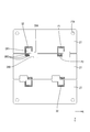
- FIG. 2 is a schematic plan view showing a circuit configuration body according to the first embodiment.
- AA sectional view of FIG. Schematic plan view showing a state in which the second circuit board is press-fitted into the bus bar
- Schematic plan view showing the adhesive sheet Schematic plan view showing a state where the adhesive sheet is adhered to the bus bar
- Schematic plan view showing the first circuit board The schematic top view which shows the state which accumulated the 1st circuit board on the adhesive sheet Schematic partial cross-sectional view showing a circuit configuration body according to a second embodiment
- the top view which shows the state by which the solder resist film was printed on the bus bar Schematic plan view showing a state where the adhesive sheet is adhered to the bus bar
- the schematic top view which shows the state which accumulated the 1st circuit board on the adhesive sheet Schematic plan view showing a circuit configuration body according to the second embodiment.
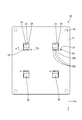
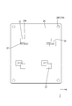
- the electrical junction box 10 is arranged in a power supply path between a power source such as a vehicle battery and a load composed of in-vehicle electrical components such as a lamp and a wiper, and is used for, for example, a DC-DC converter or an inverter. Can do.
- a power source such as a vehicle battery
- a load composed of in-vehicle electrical components such as a lamp and a wiper
- DC-DC converter or an inverter an inverter.
- the electrical junction box 10 includes a circuit configuration body 20 and a case 11 that houses the circuit configuration body 20.
- the case 11 includes a heat dissipation member 12 on which the circuit structure 20 is placed, and a cover 15 that covers the upper side of the circuit structure 20.
- the heat dissipating member 12 is made of a metal material having high thermal conductivity such as an aluminum alloy, and has a flat upper surface large enough to mount the entire substrate 21, and a plurality of heat dissipating members 12 arranged in a comb blade shape on the bottom surface side.
- the heat dissipating fins 13 are provided.
- a screw hole 14 having a screw groove for screwing with a screw 41 is formed on the upper surface of the heat radiating member 12.
- the cover 15 is made of synthetic resin or metal and has a box shape with an opening on the lower side.
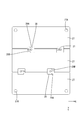
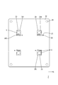
- the circuit structure 20 includes a substrate 21 and an electronic component 36 mounted on the substrate 21.
- the board 21 is arranged on the same layer as the first circuit board 22, the plurality of bus bars 27 stacked on the back surface of the first circuit board 22, and the back surface of the first circuit board 22.
- a second circuit board 30 is arranged on the same layer as the first circuit board 22, the plurality of bus bars 27 stacked on the back surface of the first circuit board 22, and the back surface of the first circuit board 22.
- a second circuit board 30 is arranged on the same layer as the first circuit board 22, the plurality of bus bars 27 stacked on the back surface of the first circuit board 22, and the back surface of the first circuit board 22.
- the first circuit board 22 is an insulating plate made of an insulating material, and a conductive path (not shown) made of copper foil or the like is formed on the upper surface of the first circuit board 22 by a printed wiring technique.
- the electronic component 36 is inserted, and the connection opening 23 connected to the corresponding bus bar 27, the through hole 24, and the through hole 26 through which the shaft portion of the screw 41 passes. It is formed (see FIGS. 2 and 7).
- the back surface of the first circuit board 22 is a surface opposite to the surface on the side where the electronic component 36 is inserted into the connection opening 23, in other words, the upper surface (front surface) on which the conductive path is formed. This is the opposite side.
- the first circuit board 22 is an example of a “circuit board”.
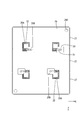
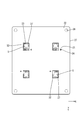
- connection openings 23 are rectangular, and a plurality (four in this embodiment) are formed at positions away from the center and the peripheral edge of the first circuit board 22 (see FIG. 7).
- a plurality of (four in the present embodiment) through-holes 24 are formed at positions separated by a predetermined dimension in the vicinity of each connection opening 23.
- Conductive relay portions 25 are formed on the inner wall surface and upper and lower opening edges of each through hole 24. The relay unit 25 is electrically connected to the conductive path on the upper surface (front surface) of the first circuit board 22.
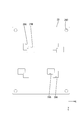
- the electronic component 36 is a so-called leadless component, and includes, for example, a plurality of N-channel MOSFETs (Field effector transistors) connected in parallel.
- the electronic component 36 (hereinafter sometimes simply referred to as “MOSFET”) has a main body 37 and a plurality of terminals 38.
- the plurality of terminals 38 include a drain terminal 38D (an example of “connection terminal”), a gate terminal 38G, and a plurality of source terminals 38S (an example of “connection terminal”).
- the main body 37 has a rectangular parallelepiped shape, and is molded with a synthetic resin exterior body 37A. Terminals 38S and 38G exposed from the bottom surface side of the exterior body 37A are arranged along the bottom surface 37B of the exterior body 37A.
- the drain terminal 38D is a plate-like terminal having substantially the same size as the electronic component 36 in a plan view, and is exposed on the bottom surface 37B of the electronic component 36 (see FIG. 3).
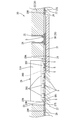
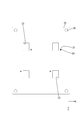
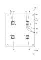
- Each bus bar 27 has a plate shape made of metal such as copper or copper alloy, and is formed by punching a metal plate material into a shape corresponding to the shape of the conductive path, and is arranged on the same plane with an interval. As shown in FIG. 4, cutout portions 28 ⁇ / b> A and 28 ⁇ / b> B are formed on the side edge of one busbar 27 of adjacent busbars 27. As shown in FIG. 6, the second circuit board 30 is press-fitted into the notches 28A and 28B. A plurality of bus bars 27 are formed with through holes 27 ⁇ / b> A through which the shafts of the screws 41 pass.
- the opposing surface 27S of the bus bar 27 facing the first circuit board 22 includes a soldering region SR1 to which the drain terminal 38D is soldered and a soldering region SR2 to which the plurality of source terminals 38S are soldered (FIG. 8).
- an adhesive sheet 29 is provided between the first circuit board 22 and the plurality of bus bars 27.
- the adhesive sheet 29 has an insulating property and is adhered to the facing surface 27 ⁇ / b> S facing the first circuit board 22 of the plurality of bus bars 27. Note that.
- the adhesive sheet 29 has adhesiveness only on the back surface 29 ⁇ / b> R facing the plurality of bus bars 27.
- the adhesive sheet 29 is smaller than the connection opening 23 in plan view and larger than the soldering area (SR1, SR2) of the bus bar 27 at a position corresponding to each connection opening 23 of the first circuit board 22.
- An opening 29A is provided.
- the sheet opening 29A is an example of “a pattern surrounding a soldering area of a bus bar to which the connection terminals are soldered”.
- the adhesive sheet 29 has a substrate opening 29B that is continuous with the sheet opening 29A.
- An example of the boundary between the sheet opening 29A and the substrate opening 29B is indicated by a two-dot chain line (virtual line) (see FIG. 5).
- a through hole 29C through which the shaft portion of the screw 41 passes is formed.
- the adhesive sheet 29 located at the boundary with the sheet opening 29A in other words, the end portion 29W of the adhesive sheet 29 forming the sheet opening 29A is soldered on the opposing surfaces 27S of the plurality of bus bars 27.
- the sheet opening 29A surrounds the soldering area (SR1, SR2) of the bus bar 27.
- the electronic component 36 is soldered by reflow.
- the end portion 29W of the adhesive sheet 29 restricts the spread of the solder S, particularly when the drain terminal 38D of the electronic component 36 is reflow soldered to the corresponding bus bar 27. That is, the drain terminal 38D has a large terminal area and a large amount of solder for soldering. Therefore, the MOSFET 36 is likely to move with the movement of the melted solder S during reflow.
- the opening area of the adhesive sheet 29 is formed smaller than usual, and the adhesive sheet 29 reaches closer to the drain terminal 38D of the MOSFET 36. (See FIG. 3).
- the adhesive sheet 29 that restricts the movement of the solder S when the MOSFET 36 is soldered to the bus bar 27 is an example of a “solder restricting layer”.
- the second circuit board 30 is a small board for connecting the gate terminal 38G of the MOSFET 36.
- a conductive path 31 made of copper foil or the like is formed on the upper surface of the second circuit board 30.
- the conductive path 31 is connected to a conductive path (not shown) formed on the surface of the first circuit board 22 via the relay portion 25 of the through hole 24.
- the gate terminal 38G and the conductive path 31, and the conductive path 31 and the relay portion 25 are soldered.
- the second circuit board 30 is press-fitted into the notches 28A and 28B of the bus bar 27 to form the bus bar 27 with the second circuit board.
- the bus bar 27 adjacent to the bus bar 27 with the second circuit board is disposed in close contact with the second circuit board 30.
- the back surface 29R of the adhesive sheet 29 shown in FIG. 5 is pressure-bonded to the front surface (opposing surface) 27S of the bus bar 27 (see FIG. 6).
- solder paste S is applied to the bus bar 27 and a predetermined position of the second circuit board 30, and the first circuit board 22 is overlaid on the adhesive sheet 29 (see FIG. 8).
- the MOSFET 36 is soldered to a predetermined bus bar 27 through a reflow furnace. Accordingly, the plurality of terminals 38D, 38G, and 38S of the MOSFET 36 are soldered to the predetermined bus bar 27 with the solder S, and the relay portion 25 is soldered to the conductive path 31 of the second circuit board 30 with the solder S. As a result, the circuit structure 20 shown in FIGS. 2 and 3 is formed.
- the circuit structure 20 is placed on the heat dissipation member 12 through the insulating layer 40. Then, the shaft portion of the screw 41 is passed through the washer 42, the through hole 26 of the first circuit board 22, the through hole 27A of the bus bar 27, and the like, and screwed into the screw hole 14 of the heat radiating member 12, so that the circuit structure 20 Is fixed to the heat dissipation member 12. Then, the electrical connection box 10 shown in FIG. 1 is formed by covering the circuit structure 20 with the cover 15.
- the adhesive sheet 29 (solder regulating layer) is formed.
- the spread of the solder S from the soldering regions (SR1, SR2) can be regulated by the sheet opening 29A (pattern) surrounding the soldering regions (SR1, SR2). That is, the adhesive sheet 29 provided between the first circuit board 22 and the plurality of bus bars 27 and having a sheet opening 29A for connecting the electronic component 36 is used as the solder restricting layer. be able to.
- the sheet opening 29A can be used as a pattern surrounding the soldering regions (SR1, SR2). That is, the end portion 29 ⁇ / b> W of the adhesive sheet 29 that forms the sheet opening 29 ⁇ / b> A can be used as a wall that restricts the spread of the solder S.
- the pressure-sensitive adhesive sheet 29 can be miniaturized in accordance with the miniaturization of the first circuit board 22, for example. Further, the planar shape of the sheet opening 29A can be formed with high accuracy. Therefore, when the electronic component 36 is soldered to the bus bar 27, it is possible to regulate the solder spread with high accuracy while enabling further miniaturization of the circuit component 20. Furthermore, since the solder spread can be regulated with high accuracy, the electronic component 36 can be positioned with high accuracy.
- the solder restricting layer is constituted by the adhesive sheet 29, and the adhesive sheet 29 is smaller than the connection opening 23 in a plan view at a position corresponding to the connection opening 23 and is drained.
- the sheet opening 29A is larger than the soldering area (SR1, SR2) of the bus bar to which the terminal 38D and the source terminal 38S are soldered (see FIG. 8). Therefore, the sheet opening 29A can be used as a pattern surrounding the soldering regions (SR1, SR2).
- Embodiment 2 will be described with reference to FIGS. 9 to 13. Only the configuration different from that of the first embodiment will be described, and the same configuration as that of the first embodiment will be denoted by the same reference numerals and the description thereof will be omitted.
- 9 is a partial cross-sectional view of a portion corresponding to FIG. 3 of the circuit configuration body 20A of the second embodiment.
- the configuration of the solder restricting layer is different from that of the first embodiment. That is, in the second embodiment, the solder restricting layer is configured by the solder resist film 32 printed on the facing surface 27S facing the electronic components 36 of the plurality of bus bars 27. At that time, the solder resist film 32 is formed as a pattern surrounding the soldered regions (SR1, SR2).
- the solder resist film 32 is an example of “a pattern surrounding a soldering area of a bus bar to which the connection terminals are soldered”.
- the solder resist film 32 includes a first pattern P1 surrounding the soldering region SR1 to which the drain terminal 38D of the MOSFET 36 is soldered, and a soldering region to which the source terminal 38S is soldered. And a second pattern P2 surrounding SR2.
- the sheet opening 29A of the adhesive sheet 29 has a larger shape than the connection opening 23 in a plan view. (See FIGS. 11 and 13).
- solder resist films 32 having patterns P1 and P2 surrounding the soldering regions SR1 and SR2 to which the connection terminals 38 of the MOSFET 36 are soldered are printed. To form.
- the second circuit board 30 is press-fitted into the notches 28A and 28B of the bus bar 27 to form the bus bar 27 with the second circuit board.
- the back surface 29R of the pressure-sensitive adhesive sheet 29 is bonded to the front surface 27S of the bus bar 27 (see FIG. 11).
- the solder paste S is applied to the bus bar 27 and a predetermined position of the second circuit board 30, and the first circuit board 22 is overlaid on the adhesive sheet 29 (see FIG. 12).
- the MOSFET 36 is soldered to a predetermined bus bar 27 through a reflow furnace. Accordingly, the plurality of terminals 38D, 38G, and 38S of the MOSFET 36 are soldered to the predetermined bus bar 27 with the solder S, and the relay portion 25 is soldered to the conductive path 31 of the second circuit board 30 with the solder S. As a result, the circuit structure 20A shown in FIG. 9 is formed.
- the circuit structure 20A is placed on the heat dissipation member 12 with the insulating layer 40 interposed therebetween. Then, the shaft portion of the screw 41 is passed through the washer 42, the through hole 26 of the first circuit board 22, the through hole 27A of the bus bar 27, and the like, and screwed into the screw hole 14 of the heat radiating member 12, so that the circuit structure 20 Is fixed to the heat dissipation member 12. Then, the electrical connection box 10 is formed by covering the circuit structure 20 with the cover 15 (see FIG. 1).
- the solder resist film 32 is formed as a pattern that surrounds the soldering regions (SR1, SR2) of the bus bar 27.
- the solder resist film 32 does not have affinity with the solder S, that is, the solder resist film 32 does not have solder wettability. Therefore, the solder resist film 32 can repel the solder S, whereby the solder resist film 32 can restrict the spread of the solder S from the soldering regions (SR1, SR2).
- the solder resist film 32 can be formed with high accuracy according to the size of the electronic component 36. Therefore, when the electronic component 36 is soldered to the bus bar 27, it is possible to regulate the solder spread with high accuracy while enabling further miniaturization of the circuit component 20. Furthermore, since the solder spread can be regulated with high accuracy, the electronic component 36 can be positioned with high accuracy.
- the pressure-sensitive adhesive sheet 29 is configured to have adhesiveness (adhesive) only on the back surface 29R. It is good also as a structure which has.
- the planar shape of the sheet opening 29A is not limited to the one shown in FIG. 5 (the planar shape larger than the region SR1 and the region SR2).
- the planar shape may be smaller than the connection opening 23 and larger than the region SR1 of the bus bar 27 where only the drain terminal (or the source terminal depending on the MOSFET type or the like) is soldered.
- the shape of the sheet opening 29A may be smaller than the connection opening 23 in a plan view and larger than the area of the bus bar to which the connection terminal of the electronic component is soldered.
- the solder regulation layer may be constituted by an adhesive sheet. That is, the circuit structure has an insulating property, and is provided between the circuit board and the plurality of bus bars 27, and includes an adhesive sheet that attaches the circuit board and the plurality of bus bars.
- the solder restricting layer is composed of an adhesive sheet, and the adhesive sheet is smaller than the connection opening 23 in plan view and is soldered to the bus bar 27 in a position corresponding to the connection opening 23 of the circuit board as a pattern. It is good also as a structure which has a sheet
- the second circuit board 30 is provided and the gate terminal 38G of the MOSFET 36 is connected to the second circuit board 30.
- the present invention is not limited to this.
- the MOSFET 36 an N-channel MOSFET having a configuration in which only the drain terminal 38D is provided on the back surface and connected to the bus bar 27 may be used.
- the gate terminal 38G and the source terminal 38S are connected to predetermined wiring on the surface side of the first circuit board 22, the second circuit board 30, the through hole 24, and the like are omitted.
- the pattern of the solder resist film 32 to be pattern printed is not limited to that shown in FIG.
- the second pattern P2 (solder resist film 32) surrounding the region R2 to which the source terminal 38S is soldered may be omitted. This is because the amount of solder required for soldering the source terminal 38S is smaller than that of the drain terminal 38D.
- the electronic component 36 is not limited to the N-channel MOSFET, and various electronic components can be used.
- it may be a P-channel MOSFET, a mechanical relay, a coil, a capacitor, or the like.
- SYMBOLS 10 Electric junction box 11 ... Case 20, 20A ... Circuit structure 22 ... 1st circuit board (circuit board) 23 ... Connection opening 27 ... Bus bar 29 ... Adhesive sheet (solder regulating layer) 29A ... Sheet opening (pattern) 32.
Abstract
回路構成体(20)は、接続用開口部(23)を有する回路基板(22)と、回路基板(22)の裏面側に設けられた複数のバスバー(27)と、接続用開口部(23)を通して露出された対応するバスバー(27)に半田付される接続端子(38D、38S)を有する電子部品(36)と、回路基板(22)と複数のバスバー(27)との間に設けられ、接続端子(38D、38S)が半田付されるバスバーの半田付領域(SR1)を取り囲むパターン(29A)を有する半田規制層(29)と、を備える。
Description
本明細書では、回路構成体および当該回路構成体を備えた電気接続箱に関し、詳しくは、回路構成体が備える回路基板に含まれる電子部品と、バスバーとを半田付する技術に関する。
従来、上記電子部品と、バスバーとを半田付する技術として、例えば、特許文献1に記載のものが知られている。特許文献1には、バスバーに半導体スイッチング素子等の電子部品を半田付する際に、半田拡がりを規制して、電子部品を精度良く正規の実装面に位置させるために、電子部品の裏面に設けられた接続端子の外縁に沿う外側のバスバーのスリットあるいは小穴からなる打抜部を設ける技術が開示されている。その際、その打抜部によって、バスバーの端子実装面上に塗布されるベースト状の半田の拡がりが遮断される。それによって、半田に表面張力による膨らみを発生させ、この膨らみを端子外面に押し当てて正規の実装位置からズレることなく、電子部品をバスバーに実装するようにしている。
しかしながら、上記従来の技術では、正規の実装位置からズレることなく、電子部品をバスバーに実装できるものの、バスバーにスリットあるいは小穴からなる打抜部を設けるためのスペースが必要とされる。そのため、回路構成体の更なる小型化にとっては不都合であった。また、半田の表面張力を利用しているため、精度良く半田拡がりを規制することは容易とは言えなかった。
本明細書に開示される技術は上記のような事情に基づいて完成されたものであって、本明細書は、電子部品をバスバーに半田付けする際に、回路構成体の更なる小型化を可能にしつつ精度良く半田拡がりを規制することができる回路構成体を提供する。
本明細書に開示される回路構成体は、接続用開口部を有する回路基板と、前記回路基板の裏面側に設けられた複数のバスバーと、前記接続用開口部を通して露出された対応するバスバーに半田付される接続端子を有する電子部品と、前記回路基板と前記複数のバスバーとの間に設けられ、前記接続端子が半田付される前記バスバーの半田付領域を取り囲むパターンを有する半田規制層と、を備える。
本構成によれば、電子部品の接続端子をバスバーの半田付領域に半田付する際に、半田規制層が有する、半田付領域を取り囲むパターンによって半田付領域からの半田の拡がりを規制することができる。半田規制層として、例えば、通常、使用される、回路基板と複数のバスバーとの間に設けられ、電子部品の接続のための開口部を有する粘着シートあるいは接着シート等を利用することができる。その際、開口部を、半田付領域を取り囲むパターンとして利用できる。すなわち、開口部を形成する粘着シートあるいは接着シートの端部を半田の拡がりを規制する壁として利用できる。
粘着シートあるいは接着シート等は、例えば、回路基板の小型化に応じて小型化できる。また、開口部の平面形状は精度良く形成することができる。そのため、電子部品をバスバーに半田付けする際に、回路構成体の更なる小型化を可能にしつつ精度良く半田拡がりを規制することができる。さらに、精度良く半田拡がりを規制することができるため、電子部品の位置決めも精度良くできる。
粘着シートあるいは接着シート等は、例えば、回路基板の小型化に応じて小型化できる。また、開口部の平面形状は精度良く形成することができる。そのため、電子部品をバスバーに半田付けする際に、回路構成体の更なる小型化を可能にしつつ精度良く半田拡がりを規制することができる。さらに、精度良く半田拡がりを規制することができるため、電子部品の位置決めも精度良くできる。
上記回路構成体において、絶縁性を有し、前記回路基板と前記複数のバスバーとの間に配置され、前記複数のバスバーの、前記回路基板に対向する対向面に粘着される粘着シートを備え、前記半田規制層は、前記粘着シートによって構成され、前記粘着シートは、前記パターンとして、前記回路基板の接続用開口部に対応した位置に、平面視において前記接続用開口部より小さく、前記接続端子が半田付される前記バスバーの前記半田付領域より大きいシート開口部を有するようにしてよい。
本構成によれば、半田規制層は、粘着シートによって構成され、粘着シートは、パターンとして、接続用開口部に対応した位置に、平面視において接続用開口部より小さく、接続端子が半田付されるバスバーの半田付領域より大きいシート開口部を有する。そのため、シート開口部を、半田付領域を取り囲むパターンとして利用できる。すなわち、シート開口部を形成する粘着シートの端部を半田の拡がりを規制する壁として利用できる。
本構成によれば、半田規制層は、粘着シートによって構成され、粘着シートは、パターンとして、接続用開口部に対応した位置に、平面視において接続用開口部より小さく、接続端子が半田付されるバスバーの半田付領域より大きいシート開口部を有する。そのため、シート開口部を、半田付領域を取り囲むパターンとして利用できる。すなわち、シート開口部を形成する粘着シートの端部を半田の拡がりを規制する壁として利用できる。
また、上記回路構成体において、絶縁性を有し、前記回路基板と前記複数のバスバーとの間に配置され、前記回路基板と前記複数のバスバーとを貼り付ける接着シートを備え、前記半田規制層は、前記接着シートによって構成され、前記接着シートは、前記パターンとして、前記回路基板の前記接続用開口部に対応した位置に、平面視において前記接続用開口部より小さく、前記接続端子が半田付される前記バスバーの半田付領域より大きいシート開口部を有するようにしてよい。
本構成によれば、半田規制層は、接着シートによって構成され、接着シートは、パターンとして、接続用開口部に対応した位置に、平面視において接続用開口部より小さく、接続端子が半田付されるバスバーの半田付領域より大きいシート開口部を有する。そのため、この場合であっても、シート開口部を、半田付領域を取り囲むパターンとして利用できる。すなわち、シート開口部を形成する接着シートの端部を半田の拡がりを規制する壁として利用できる。
本構成によれば、半田規制層は、接着シートによって構成され、接着シートは、パターンとして、接続用開口部に対応した位置に、平面視において接続用開口部より小さく、接続端子が半田付されるバスバーの半田付領域より大きいシート開口部を有する。そのため、この場合であっても、シート開口部を、半田付領域を取り囲むパターンとして利用できる。すなわち、シート開口部を形成する接着シートの端部を半田の拡がりを規制する壁として利用できる。
また、上記回路構成体において、前記半田規制層は、前記複数のバスバーの前記電子部品に対向する対向面上に印刷された半田レジスト膜によって構成され、前記半田レジスト膜は、前記半田付領域を取り囲む前記パターンとして形成されているようにしてもよい。
本構成によれば、半田レジスト膜が、バスバーの半田付領域を取り囲むパターンとして形成されている。半田レジスト膜は、半田との親和性を有さない、すなわち、半田レジスト膜は半田濡れ性を有さない。そのため、半田レジスト膜は半田を弾くことができ、それによって、半田レジスト膜は、半田付領域から半田が拡がることを規制することができる。
本構成によれば、半田レジスト膜が、バスバーの半田付領域を取り囲むパターンとして形成されている。半田レジスト膜は、半田との親和性を有さない、すなわち、半田レジスト膜は半田濡れ性を有さない。そのため、半田レジスト膜は半田を弾くことができ、それによって、半田レジスト膜は、半田付領域から半田が拡がることを規制することができる。
また、本明細書に開示される電気接続箱は、上記いずれかの回路構成体と、前記回路構成体を収容するケースと、を備える。
本発明によれば、電子部品をバスバーに半田付けする際に、回路構成体の更なる小型化を可能にしつつ精度良く半田拡がりを規制することができる。
<実施形態1>
実施形態1を図1から図8までを参照しつつ説明する。
実施形態1を図1から図8までを参照しつつ説明する。
電気接続箱10は、例えば、車両のバッテリ等の電源と、ランプ、ワイパー等の車載電装品等からなる負荷との間の電力供給経路に配され、例えばDC-DCコンバータやインバータ等に用いることができる。以下では、X方向を右方、Y方向を前方、Z方向を上方として説明する。
1.電気接続箱
電気接続箱10は、図1に示すように、回路構成体20と、回路構成体20を収容するケース11とを備える。ケース11は、回路構成体20が載置される放熱部材12と、回路構成体20の上方側を覆うカバー15とを備えている。
電気接続箱10は、図1に示すように、回路構成体20と、回路構成体20を収容するケース11とを備える。ケース11は、回路構成体20が載置される放熱部材12と、回路構成体20の上方側を覆うカバー15とを備えている。
放熱部材12はアルミニウム合金等の熱伝導性が高い金属材料からなり、基板21の全体を載置可能な大きさの平坦な上面を有し、底面側に櫛刃状に並んで配された複数の放熱フィン13を有している。放熱部材12の上面には、ネジ41でネジ留めするためのネジ溝を有するネジ孔14が形成されている。カバー15は、合成樹脂製又は金属製であって、下方側が開口した箱形である。
2.回路構成体
回路構成体20は、図2,図3に示すように、基板21と、基板21に実装される電子部品36とを備える。基板21は、第1回路基板22と、第1回路基板22の裏面に重ねられた複数のバスバー27と、第1回路基板22の裏面に重ねられ、複数のバスバー27と同層に配された第2回路基板30とを備えている。
回路構成体20は、図2,図3に示すように、基板21と、基板21に実装される電子部品36とを備える。基板21は、第1回路基板22と、第1回路基板22の裏面に重ねられた複数のバスバー27と、第1回路基板22の裏面に重ねられ、複数のバスバー27と同層に配された第2回路基板30とを備えている。
第1回路基板22は、絶縁材料からなる絶縁板であり、第1回路基板22の上面にはプリント配線技術により銅箔等からなる導電路(図示しない)が形成されている。また、第1回路基板22には、電子部品36が挿通され、対応するバスバー27に接続される接続用開口部23と、スルーホール24と、ネジ41の軸部を通す通し孔26とが貫通形成されている(図2および図7参照)。第1回路基板22の裏面とは、接続用開口部23に電子部品36を挿入する側の面と反対側の面であり、言い換えれば、上記導電路が形成されている上面(表面)とは反対側の面である。第1回路基板22は、「回路基板」の一例である。
接続用開口部23は、長方形状であって、第1回路基板22の中央部及び周縁部から離れた位置に複数(本実施形態では4つ)形成されている(図7参照)。スルーホール24は、各接続用開口部23の近傍の所定寸法離れた位置に、複数(本実施形態では4つ)形成されている。各スルーホール24の内壁面および上下の開口縁部には、導電性の中継部25が形成されている。中継部25は、第1回路基板22の上面(表面)の導電路と電気的に接続されている。
電子部品36は、本実施形態では、いわゆるリードレス部品であり、例えば、並列接続された複数のNチャネルMOSFET(Field effect transistor)によって構成される。電子部品36(以下、単に「MOSFET」と記す場合がある)は、本体37と、複数の端子38とを有する。複数の端子38は、ドレイン端子38D(「接続端子」の一例)、ゲート端子38G、および複数のソース端子38S(「接続端子」の一例)を含む。
本体37は、直方体状であって、合成樹脂製の外装体37Aでモールドされている。外装体37Aの底面側から露出する端子38S,38Gが、外装体37Aの底面37Bに沿うように配されている。一方、ドレイン端子38Dは、平面視において電子部品36とほぼ同じ大きさを有する板状の端子であり、電子部品36の底面37Bに露出して配置されている(図3参照)。
各バスバー27は、銅や銅合金等の金属からなる板状であって、金属板材を導電路の形状に応じた形状に打ち抜いて形成され、同一平面上に間隔を空けて配されている。隣り合うバスバー27の一方のバスバー27の側縁には、図4に示すように、バスバー27の側縁を切り欠いた形状の切欠部28A、28Bが形成されている。この切欠部28A、28Bには、図6に示すように、第2回路基板30が圧入される。複数のバスバー27には、ネジ41の軸部を通す通し孔27Aが貫通形成されている。また、バスバー27の第1回路基板22に対向する対向面27Sは、ドレイン端子38Dが半田付される半田付領域SR1、および複数のソース端子38Sが半田付される半田付領域SR2を含む(図8参照)。
また、第1回路基板22と複数のバスバー27との間には粘着シート29が設けられている。粘着シート29は絶縁性を有し、複数のバスバー27の第1回路基板22に対向する対向面27Sに粘着される。なお。本実施形態では、粘着シート29は、複数のバスバー27に対向する裏面29Rにのみ、粘着性を有する。
また、粘着シート29は、第1回路基板22の各接続用開口部23に対応した位置に、平面視において接続用開口部23より小さく、バスバー27の半田付領域(SR1、SR2)より大きいシート開口部29Aを有している。シート開口部29Aは、「接続端子が半田付されるバスバーの半田付領域を取り囲むパターン」の一例である。
また、粘着シート29は、シート開口部29Aと連なる基板用開口部29Bを有している。シート開口部29Aと基板用開口部29Bとの境界の例を、二点鎖線(仮想線)で示す(図5参照)。また、ネジ41の軸部を通す通し孔29Cが貫通形成されている。
また、粘着シート29は、シート開口部29Aと連なる基板用開口部29Bを有している。シート開口部29Aと基板用開口部29Bとの境界の例を、二点鎖線(仮想線)で示す(図5参照)。また、ネジ41の軸部を通す通し孔29Cが貫通形成されている。
シート開口部29Aとの境界に位置する粘着シート29は、言い換えれば、シート開口部29Aを形成する粘着シート29の端部29Wは、複数のバスバー27の対向面27S上において、半田付されるMOSFET36の端子38D、38G、38Sを囲む周辺領域に位置し、半田Sに対する壁を形成している(図3参照)。言い換えれば、シート開口部29Aは、バスバー27の半田付領域(SR1、SR2)を取り囲んでいる。なお、本実施形態では、電子部品36の半田付けは、リフローによって行われる。
粘着シート29の端部29Wは、特に、電子部品36のドレイン端子38Dを対応するバスバー27にリフロー半田付けする際に、半田Sの拡がりを規制する。すなわち、ドレイン端子38Dは端子面積が大きく、半田付けの用の半田量が多い。そのため、リフロー時に、溶けた半田Sの移動に伴ってMOSFET36が移動しやすい。そのような、リフロー時の半田の移動を規制するために、本実施形態では、粘着シート29の開口面積を通常よりも小さく形成して、粘着シート29がMOSFET36のドレイン端子38Dのより近くまで達するようにしている(図3参照)。このようにMOSFET36をバスバー27に半田付する際に半田Sの移動を規制する粘着シート29は、「半田規制層」の一例である。
第2回路基板30は、MOSFET36のゲート端子38Gを接続するための小さい基板である。第2回路基板30の上面には、銅箔等からなる導電路31が形成されている。導電路31は、スルーホール24の中継部25を介して、第1回路基板22の表面に形成された導電路(図示せず)に接続される。ゲート端子38Gと導電路31、導電路31と中継部25とは、それぞれ半田付けされる。
3.電気接続箱の製造方法
次に、図4から図8までを参照して電気接続箱10の製造方法について概略的に説明する。
次に、図4から図8までを参照して電気接続箱10の製造方法について概略的に説明する。
図4に示すように、バスバー27の切欠部28A、28Bに第2回路基板30を圧入して第2回路基板付きのバスバー27を形成する。次に、第2回路基板付きのバスバー27に隣り合うバスバー27を第2回路基板30に密着させて配置する。次に、バスバー27の表面(対向面)27Sに、図5に示される粘着シート29の裏面29Rを圧着して貼り合わせる(図6参照)。
次いで、バスバー27と、第2回路基板30の所定の位置に半田ペーストSを塗布し、第1回路基板22を粘着シート29上に重ね合わせる(図8参照)。次いで、リフロー炉を通してMOSFET36を所定のバスバー27に半田付けする。それによって、MOSFET36の複数の端子38D、38G、38Sが所定のバスバー27に半田Sで半田付けされるとともに、中継部25が第2回路基板30の導電路31に半田Sで半田付けされる。これによって、図2および図3に示される回路構成体20が形成される。
次に、放熱部材12の上に絶縁層40を介して回路構成体20を載置する。そして、ネジ41の軸部を、ワッシャー42,第1回路基板22の通し孔26,バスバー27の通し孔27A等に通し、放熱部材12のネジ孔14にネジ留めすることで、回路構成体20が放熱部材12に固定される。そして、回路構成体20の上からカバー15を被せることで、図1に示される電気接続箱10が形成される。
4.実施形態1の効果
上記実施形態1によれば、MOSFET36のドレイン端子38Dおよびソース端子38Sをバスバー27の半田付領域(SR1、SR2)に半田付する際に、粘着シート29(半田規制層)が有する、半田付領域(SR1、SR2)を取り囲むシート開口部29A(パターン)によって半田付領域(SR1、SR2)からの半田Sの拡がりを規制することができる。すなわち、半田規制層として、通常、使用される、第1回路基板22と複数のバスバー27との間に設けられ、電子部品36の接続のためのシート開口部29Aを有する粘着シート29を利用することができる。その際、シート開口部29Aを、半田付領域(SR1、SR2)を取り囲むパターンとして利用できる。すなわち、シート開口部29Aを形成する粘着シート29の端部29Wを、半田Sの拡がりを規制する壁として利用できる。
上記実施形態1によれば、MOSFET36のドレイン端子38Dおよびソース端子38Sをバスバー27の半田付領域(SR1、SR2)に半田付する際に、粘着シート29(半田規制層)が有する、半田付領域(SR1、SR2)を取り囲むシート開口部29A(パターン)によって半田付領域(SR1、SR2)からの半田Sの拡がりを規制することができる。すなわち、半田規制層として、通常、使用される、第1回路基板22と複数のバスバー27との間に設けられ、電子部品36の接続のためのシート開口部29Aを有する粘着シート29を利用することができる。その際、シート開口部29Aを、半田付領域(SR1、SR2)を取り囲むパターンとして利用できる。すなわち、シート開口部29Aを形成する粘着シート29の端部29Wを、半田Sの拡がりを規制する壁として利用できる。
粘着シート29は、例えば、第1回路基板22の小型化に応じて小型化できる。また、シート開口部29Aの平面形状は精度良く形成することができる。そのため、電子部品36をバスバー27に半田付けする際に、回路構成体20の更なる小型化を可能にしつつ精度良く半田拡がりを規制することができる。さらに、精度良く半田拡がりを規制することができるため、電子部品36の位置決めも精度良くできる。
また、実施形態1では、半田規制層は、粘着シート29によって構成され、粘着シート29は、パターンとして、接続用開口部23に対応した位置に、平面視において接続用開口部23より小さく、ドレイン端子38Dおよびソース端子38Sが半田付されるバスバーの半田付領域(SR1、SR2)より大きいシート開口部29Aを有する(図8参照)。そのため、シート開口部29Aを、半田付領域(SR1、SR2)を取り囲むパターンとして利用できる。
<実施形態2>
次に、実施形態2を、図9から図13までを参照して説明する。なお、実施形態1と異なる構成についてのみ説明し、実施形態1と同一の構成については同一の符号を付して説明を省略する。なお、図9は、実施形態2の回路構成体20Aの、図3に相当する箇所の部分断面図である。
次に、実施形態2を、図9から図13までを参照して説明する。なお、実施形態1と異なる構成についてのみ説明し、実施形態1と同一の構成については同一の符号を付して説明を省略する。なお、図9は、実施形態2の回路構成体20Aの、図3に相当する箇所の部分断面図である。
実施形態1とは、半田規制層の構成が異なる。すなわち、実施形態2では、半田規制層は、複数のバスバー27の電子部品36に対向する対向面27S上に印刷された半田レジスト膜32によって構成されている。その際、半田レジスト膜32は、半田付領域(SR1、SR2)を取り囲むパターンとして形成されている。半田レジスト膜32は、「接続端子が半田付されるバスバーの半田付領域を取り囲むパターン」の一例である。
詳しくは、半田レジスト膜32は、図10に示されるように、MOSFET36のドレイン端子38Dが半田付けされる半田付領域SR1を囲む第1パターンP1と、ソース端子38Sが半田付けされる半田付領域SR2を囲む第2パターンP2とを含む。
また、実施形態2においては、粘着シート29のシート開口部29Aは、平面視において接続用開口部23よりも大きい形状を有している。(図11および図13参照)。
4.電気接続箱の製造方法
次に、図10から図13を参照して、実施形態2の電気接続箱10の製造方法について概略的に説明する。
次に、図10から図13を参照して、実施形態2の電気接続箱10の製造方法について概略的に説明する。
図10に示すように、バスバー27のMOSFET36に対向する対向面27S上に、MOSFET36の接続端子38が半田付けされる半田付領域SR1、SR2をそれぞれ囲むパターンP1、P2の半田レジスト膜32を印刷して形成する。
次に、バスバー27の各切欠部28A、28Bに第2回路基板30を圧入して第2回路基板付きのバスバー27を形成する。次に、バスバー27の表面27Sに、粘着シート29の裏面29Rを圧着して貼り合わせる(図11参照)。
次いで、バスバー27と、第2回路基板30の所定の位置に半田ペーストSを塗布し、第1回路基板22を粘着シート29上に重ね合わせる(図12参照)。次いで、リフロー炉を通してMOSFET36を所定のバスバー27に半田付けする。それによって、MOSFET36の複数の端子38D、38G、38Sが所定のバスバー27に半田Sで半田付けされるとともに、中継部25が第2回路基板30の導電路31に半田Sで半田付けされる。これによって、図9に示される回路構成体20Aが形成される。
次に、実施形態1と同様に、放熱部材12の上に絶縁層40を介して回路構成体20Aを載置する。そして、ネジ41の軸部を、ワッシャー42,第1回路基板22の通し孔26,バスバー27の通し孔27A等に通し、放熱部材12のネジ孔14にネジ留めすることで、回路構成体20が放熱部材12に固定される。そして、回路構成体20の上からカバー15を被せることで、電気接続箱10が形成される(図1参照)。
5.実施形態2の効果
実施形態2では、半田レジスト膜32が、バスバー27の半田付領域(SR1、SR2)を取り囲むパターンとして形成されている。半田レジスト膜32は、半田Sとの親和性を有さない、すなわち、半田レジスト膜32は半田濡れ性を有さない。そのため、半田レジスト膜32は半田Sを弾くことができ、それによって、半田レジスト膜32は、半田付領域(SR1、SR2)から半田Sが拡がることを規制することができる。
実施形態2では、半田レジスト膜32が、バスバー27の半田付領域(SR1、SR2)を取り囲むパターンとして形成されている。半田レジスト膜32は、半田Sとの親和性を有さない、すなわち、半田レジスト膜32は半田濡れ性を有さない。そのため、半田レジスト膜32は半田Sを弾くことができ、それによって、半田レジスト膜32は、半田付領域(SR1、SR2)から半田Sが拡がることを規制することができる。
また、半田レジスト膜32は、電子部品36の大きさに応じて精度良く形成することができる。そのため、電子部品36をバスバー27に半田付けする際に、回路構成体20の更なる小型化を可能にしつつ精度良く半田拡がりを規制することができる。さらに、精度良く半田拡がりを規制することができるため、電子部品36の位置決めも精度良くできる。
<他の実施形態>
本発明は上記記述及び図面によって説明した実施形態に限定されるものではなく、例えば次のような実施形態も本発明の技術的範囲に含まれる。
本発明は上記記述及び図面によって説明した実施形態に限定されるものではなく、例えば次のような実施形態も本発明の技術的範囲に含まれる。
(1)上記実施形態1では、粘着シート29はその裏面29Rにのみ粘着性(粘着剤)を有する構成としたがこれに限られず、その表面(第1回路基板22側の面)も粘着性を有する構成としてもよい。
また、シート開口部29Aの平面形状も、図5に示されたもの(領域SR1および領域SR2より大きい平面形状)に限られない。例えば、接続用開口部23より小さく、ドレイン端子(あるいは、MOSFETの型等に応じてソース端子)のみが半田付されるバスバー27の領域SR1より大きい平面形状とされてもよい。要は、シート開口部29Aの形状は、平面視において接続用開口部23より小さく、電子部品の接続端子が半田付されるバスバーの領域より大きい形状であればよい。
また、シート開口部29Aの平面形状も、図5に示されたもの(領域SR1および領域SR2より大きい平面形状)に限られない。例えば、接続用開口部23より小さく、ドレイン端子(あるいは、MOSFETの型等に応じてソース端子)のみが半田付されるバスバー27の領域SR1より大きい平面形状とされてもよい。要は、シート開口部29Aの形状は、平面視において接続用開口部23より小さく、電子部品の接続端子が半田付されるバスバーの領域より大きい形状であればよい。
(2)上記実施形態1では、半田規制層を粘着シート29によって構成する例を示したがこれに限られない。粘着シート29に代えて接着シートによって半田規制層を構成するようにしてもよい。
すなわち、回路構成体は、絶縁性を有し、回路基板と複数のバスバー27との間に配置され、回路基板と複数のバスバーとを貼り付ける接着シートを備える。そして、半田規制層は、接着シートによって構成され、接着シートは、パターンとして、回路基板の接続用開口部23に対応した位置に、平面視において接続用開口部23より小さく、バスバー27の半田付領域(SR1、SR2)より大きいシート開口部を有する構成としてもよい。
この場合であっても、シート開口部を、半田付領域(SR1、SR2)を取り囲むパターンとして利用できる。すなわち、シート開口部を形成する接着シートの端部を半田Sの拡がりを規制する壁として利用できる。
すなわち、回路構成体は、絶縁性を有し、回路基板と複数のバスバー27との間に配置され、回路基板と複数のバスバーとを貼り付ける接着シートを備える。そして、半田規制層は、接着シートによって構成され、接着シートは、パターンとして、回路基板の接続用開口部23に対応した位置に、平面視において接続用開口部23より小さく、バスバー27の半田付領域(SR1、SR2)より大きいシート開口部を有する構成としてもよい。
この場合であっても、シート開口部を、半田付領域(SR1、SR2)を取り囲むパターンとして利用できる。すなわち、シート開口部を形成する接着シートの端部を半田Sの拡がりを規制する壁として利用できる。
(3)上記各実施形態では、第2回路基板30を設け、MOSFET36のゲート端子38Gを第2回路基板30に接続する構成を示したがこれに限られない。例えば、MOSFET36として、ドレイン端子38Dのみが裏面に設けられ、バスバー27に接続される構成のNチャネルMOSFETを使用してもよい。この場合、ゲート端子38Gおよびソース端子38Sは第1回路基板22の表面側で所定の配線に接続されるため、第2回路基板30、スルーホール24等は省略される。
(4)上記実施形態2において、パターン印刷される半田レジスト膜32のパターンは、図10に示されたものに限られない。例えば、ソース端子38Sが半田付けされる領域R2を囲む第2パターンP2(半田レジスト膜32)は、省略されてもよい。ソース端子38Sの半田付けに要する半田量は、ドレイン端子38Dの半田量に比べて少ないためである。
(5)上記各実施形態では、電子部品36としては、NチャネルMOSFETに限られず、種々の電子部品を用いることができる。例えば、PチャネルMOSFET、メカニカルリレー、コイル、コンデンサ等としてもよい。
10…電気接続箱
11…ケース
20、20A…回路構成体
22…第1回路基板(回路基板)
23…接続用開口部
27…バスバー
29…粘着シート(半田規制層)
29A…シート開口部(パターン)
32…半田レジスト膜(半田規制層、パターン)
36…NチャネルMOSFET(電子部品)
38D…ドレイン端子(接続端子)
38S…ソース端子(接続端子)
SR1、SR2…半田付領域
11…ケース
20、20A…回路構成体
22…第1回路基板(回路基板)
23…接続用開口部
27…バスバー
29…粘着シート(半田規制層)
29A…シート開口部(パターン)
32…半田レジスト膜(半田規制層、パターン)
36…NチャネルMOSFET(電子部品)
38D…ドレイン端子(接続端子)
38S…ソース端子(接続端子)
SR1、SR2…半田付領域
Claims (5)
- 接続用開口部を有する回路基板と、
前記回路基板の裏面側に設けられた複数のバスバーと、
前記接続用開口部を通して露出された対応するバスバーに半田付される接続端子を有する電子部品と、
前記回路基板と前記複数のバスバーとの間に設けられ、前記接続端子が半田付される前記バスバーの半田付領域を取り囲むパターンを有する半田規制層と、
を備えた、回路構成体。 - 請求項1に記載の回路構成体において、
絶縁性を有し、前記回路基板と前記複数のバスバーとの間に配置され、前記複数のバスバーの、前記回路基板に対向する対向面に粘着される粘着シートを備え、
前記半田規制層は、前記粘着シートによって構成され、
前記粘着シートは、前記パターンとして、前記回路基板の前記接続用開口部に対応した位置に、平面視において前記接続用開口部より小さく、前記バスバーの前記半田付領域より大きいシート開口部を有する、回路構成体。 - 請求項1に記載の回路構成体において、
絶縁性を有し、前記回路基板と前記複数のバスバーとの間に配置され、前記回路基板と前記複数のバスバーとを貼り付ける接着シートを備え、
前記半田規制層は、前記接着シートによって構成され、
前記接着シートは、前記パターンとして、前記回路基板の前記接続用開口部に対応した位置に、平面視において前記接続用開口部より小さく、前記バスバーの前記半田付領域より大きいシート開口部を有する、回路構成体。 - 請求項1に記載の回路構成体において、
前記半田規制層は、前記複数のバスバーの前記電子部品に対向する対向面上に印刷された半田レジスト膜によって構成され、
前記半田レジスト膜は、前記半田付領域を取り囲む前記パターンとして形成されている、回路構成体。 - 請求項1から請求項4のいずれか一項に記載の回路構成体と、
前記回路構成体を収容するケースと、
を備える、電気接続箱。
Priority Applications (3)
| Application Number | Priority Date | Filing Date | Title |
|---|---|---|---|
| CN201680049628.8A CN108029216B (zh) | 2015-09-15 | 2016-08-30 | 电路结构体及电连接箱 |
| DE112016004181.0T DE112016004181T5 (de) | 2015-09-15 | 2016-08-30 | Schaltungsanordnung und elektrischer Verteilerkasten |
| US15/759,604 US10334734B2 (en) | 2015-09-15 | 2016-08-30 | Circuit assembly and electrical junction box |
Applications Claiming Priority (2)
| Application Number | Priority Date | Filing Date | Title |
|---|---|---|---|
| JP2015-181828 | 2015-09-15 | ||
| JP2015181828A JP6528620B2 (ja) | 2015-09-15 | 2015-09-15 | 回路構成体および電気接続箱 |
Publications (1)
| Publication Number | Publication Date |
|---|---|
| WO2017047373A1 true WO2017047373A1 (ja) | 2017-03-23 |
Family
ID=58288895
Family Applications (1)
| Application Number | Title | Priority Date | Filing Date |
|---|---|---|---|
| PCT/JP2016/075287 WO2017047373A1 (ja) | 2015-09-15 | 2016-08-30 | 回路構成体および電気接続箱 |
Country Status (5)
| Country | Link |
|---|---|
| US (1) | US10334734B2 (ja) |
| JP (1) | JP6528620B2 (ja) |
| CN (1) | CN108029216B (ja) |
| DE (1) | DE112016004181T5 (ja) |
| WO (1) | WO2017047373A1 (ja) |
Families Citing this family (7)
| Publication number | Priority date | Publication date | Assignee | Title |
|---|---|---|---|---|
| JP6432792B2 (ja) * | 2015-09-29 | 2018-12-05 | 株式会社オートネットワーク技術研究所 | 回路構成体及び電気接続箱 |
| JP6939542B2 (ja) * | 2017-12-28 | 2021-09-22 | 株式会社オートネットワーク技術研究所 | 電気接続装置 |
| JP6958515B2 (ja) * | 2018-09-03 | 2021-11-02 | 株式会社オートネットワーク技術研究所 | 回路構造体及び電気接続箱 |
| DE102019101973A1 (de) * | 2019-01-28 | 2020-07-30 | Eugen Forschner Gmbh | Verbindungsanordnung zum Verbinden einer Stromschiene mit einem Gehäuse |
| JP7135999B2 (ja) * | 2019-05-13 | 2022-09-13 | 株式会社オートネットワーク技術研究所 | 配線基板 |
| US11382241B2 (en) * | 2019-09-25 | 2022-07-05 | Baidu Usa Llc | Cooling devices for edge computing and heterogeneous computing electronics hardware |
| US11778793B2 (en) * | 2021-03-31 | 2023-10-03 | Toyota Motor Engineering & Manufacturing North America, Inc. | Systems including an integrated power module with vias and methods of forming the same |
Citations (4)
| Publication number | Priority date | Publication date | Assignee | Title |
|---|---|---|---|---|
| JPH05327166A (ja) * | 1992-05-26 | 1993-12-10 | Hitachi Ltd | 電子部品実装方法 |
| JPH07254775A (ja) * | 1994-03-16 | 1995-10-03 | Sankyo Seiki Mfg Co Ltd | 回路基板 |
| JPH08250625A (ja) * | 1995-03-09 | 1996-09-27 | Citizen Watch Co Ltd | 樹脂封止型半導体装置 |
| JP2004147416A (ja) * | 2002-10-23 | 2004-05-20 | Auto Network Gijutsu Kenkyusho:Kk | 回路体の形成方法 |
Family Cites Families (19)
| Publication number | Priority date | Publication date | Assignee | Title |
|---|---|---|---|---|
| JP2536657B2 (ja) * | 1990-03-28 | 1996-09-18 | 三菱電機株式会社 | 電気装置及びその製造方法 |
| JPH0442597A (ja) * | 1990-06-08 | 1992-02-13 | Matsushita Electric Works Ltd | セラミック多層配線板の製造方法 |
| JPH08116153A (ja) * | 1994-10-14 | 1996-05-07 | Sony Corp | プリント基板とプリント基板製造方法 |
| US6518868B1 (en) * | 2000-08-15 | 2003-02-11 | Galaxy Power, Inc. | Thermally conducting inductors |
| BRPI0100051B1 (pt) * | 2001-01-11 | 2016-11-29 | Brasil Compressores Sa | gabinete de dispositivo eletrônico |
| DE10129788B4 (de) * | 2001-06-20 | 2005-11-10 | Siemens Ag | Kunststoffrahmen zur Montage eines elektronischen Starkstrom-Steuergeräts |
| US6724631B2 (en) * | 2002-04-22 | 2004-04-20 | Delta Electronics Inc. | Power converter package with enhanced thermal management |
| JP4261213B2 (ja) * | 2003-02-14 | 2009-04-30 | 株式会社オートネットワーク技術研究所 | 回路構成体の製造方法 |
| TWI230425B (en) * | 2004-02-06 | 2005-04-01 | South Epitaxy Corp | Bumping process for light emitting diode |
| TWI267173B (en) * | 2004-03-29 | 2006-11-21 | Sanyo Electric Co | Circuit device and method for manufacturing thereof |
| US7310233B2 (en) * | 2005-01-28 | 2007-12-18 | Tyco Electronics Power Systems | Apparatus and method for transferring heat from an electrical module |
| US20090103267A1 (en) * | 2007-10-17 | 2009-04-23 | Andrew Dean Wieland | Electronic assembly and method for making the electronic assembly |
| JP5512082B2 (ja) * | 2007-12-17 | 2014-06-04 | 株式会社東芝 | 半導体装置の製造方法及び半導体装置 |
| DE102009054517B4 (de) * | 2009-12-10 | 2011-12-29 | Robert Bosch Gmbh | Elektronisches Steuergerät |
| DE102011012673A1 (de) * | 2010-03-17 | 2011-09-22 | Hitachi Automotive Systems, Ltd. | Elektronische Steuereinrichtung für Fahrzeuge |
| JP5408502B2 (ja) * | 2010-09-06 | 2014-02-05 | 株式会社デンソー | 電子制御ユニット |
| JP5893455B2 (ja) * | 2012-03-19 | 2016-03-23 | 日清紡ホールディングス株式会社 | 電子部品の製造方法 |
| KR101407194B1 (ko) * | 2013-05-10 | 2014-06-12 | 현대오트론 주식회사 | 차량의 전자제어장치 |
| JP6278695B2 (ja) * | 2013-12-26 | 2018-02-14 | 株式会社デンソー | 電子制御ユニット、および、これを用いた電動パワーステアリング装置 |
-
2015
- 2015-09-15 JP JP2015181828A patent/JP6528620B2/ja active Active
-
2016
- 2016-08-30 US US15/759,604 patent/US10334734B2/en active Active
- 2016-08-30 WO PCT/JP2016/075287 patent/WO2017047373A1/ja active Application Filing
- 2016-08-30 CN CN201680049628.8A patent/CN108029216B/zh active Active
- 2016-08-30 DE DE112016004181.0T patent/DE112016004181T5/de active Pending
Patent Citations (4)
| Publication number | Priority date | Publication date | Assignee | Title |
|---|---|---|---|---|
| JPH05327166A (ja) * | 1992-05-26 | 1993-12-10 | Hitachi Ltd | 電子部品実装方法 |
| JPH07254775A (ja) * | 1994-03-16 | 1995-10-03 | Sankyo Seiki Mfg Co Ltd | 回路基板 |
| JPH08250625A (ja) * | 1995-03-09 | 1996-09-27 | Citizen Watch Co Ltd | 樹脂封止型半導体装置 |
| JP2004147416A (ja) * | 2002-10-23 | 2004-05-20 | Auto Network Gijutsu Kenkyusho:Kk | 回路体の形成方法 |
Also Published As
| Publication number | Publication date |
|---|---|
| JP2017060256A (ja) | 2017-03-23 |
| US10334734B2 (en) | 2019-06-25 |
| DE112016004181T5 (de) | 2018-05-30 |
| CN108029216A (zh) | 2018-05-11 |
| JP6528620B2 (ja) | 2019-06-12 |
| US20190045635A1 (en) | 2019-02-07 |
| CN108029216B (zh) | 2020-03-17 |
Similar Documents
| Publication | Publication Date | Title |
|---|---|---|
| WO2017047373A1 (ja) | 回路構成体および電気接続箱 | |
| US10194523B2 (en) | Circuit assembly, electrical junction box, and manufacturing method for circuit assembly | |
| US10090657B2 (en) | Circuit assembly, connected busbar structure, and electrical junction box | |
| JP6521171B2 (ja) | 回路構成体 | |
| US10263405B2 (en) | Circuit assembly and electrical junction box | |
| US10278278B2 (en) | Circuit structure | |
| US10756012B2 (en) | Circuit assembly | |
| US10880989B2 (en) | Electrical junction box | |
| CN107851984B (zh) | 电路结构体及电连接箱 | |
| US20190208617A1 (en) | Conductive member, circuit assembly, and method for manufacturing conductive member | |
| US10398019B2 (en) | Circuit structure and electrical junction box | |
| WO2018211935A1 (ja) | 回路装置 | |
| JP6119664B2 (ja) | 回路構成体および電気接続箱 | |
| JP6593597B2 (ja) | 回路構成体 | |
| CN111373525B (zh) | 电路结构体及电接线盒 | |
| US20210368618A1 (en) | Circuit assembly and electrical junction box | |
| JP2018006662A (ja) | 回路基板及び電気接続箱 | |
| JP2010110170A (ja) | 回路構成体および電気接続箱 | |
| JP2006286465A (ja) | スイッチングユニット | |
| JP6065806B2 (ja) | 回路構成体及び回路構成体の製造方法 | |
| WO2020246224A1 (ja) | 回路構成体及び電気接続箱 | |
| JP2006310557A (ja) | スイッチングユニット | |
| JP2014013809A (ja) | 半導体デバイス |
Legal Events
| Date | Code | Title | Description |
|---|---|---|---|
| 121 | Ep: the epo has been informed by wipo that ep was designated in this application |
Ref document number: 16846244 Country of ref document: EP Kind code of ref document: A1 |
|
| WWE | Wipo information: entry into national phase |
Ref document number: 112016004181 Country of ref document: DE |
|
| 122 | Ep: pct application non-entry in european phase |
Ref document number: 16846244 Country of ref document: EP Kind code of ref document: A1 |