WO2020255666A1 - Board structure - Google Patents
Board structure Download PDFInfo
- Publication number
- WO2020255666A1 WO2020255666A1 PCT/JP2020/021110 JP2020021110W WO2020255666A1 WO 2020255666 A1 WO2020255666 A1 WO 2020255666A1 JP 2020021110 W JP2020021110 W JP 2020021110W WO 2020255666 A1 WO2020255666 A1 WO 2020255666A1
- Authority
- WO
- WIPO (PCT)
- Prior art keywords
- conductive plate
- sheet
- base substrate
- wiring member
- terminal
- Prior art date
Links
Images


Classifications
-
- H—ELECTRICITY
- H05—ELECTRIC TECHNIQUES NOT OTHERWISE PROVIDED FOR
- H05K—PRINTED CIRCUITS; CASINGS OR CONSTRUCTIONAL DETAILS OF ELECTRIC APPARATUS; MANUFACTURE OF ASSEMBLAGES OF ELECTRICAL COMPONENTS
- H05K1/00—Printed circuits
- H05K1/02—Details
- H05K1/0201—Thermal arrangements, e.g. for cooling, heating or preventing overheating
- H05K1/0203—Cooling of mounted components
- H05K1/0207—Cooling of mounted components using internal conductor planes parallel to the surface for thermal conduction, e.g. power planes
-
- H—ELECTRICITY
- H05—ELECTRIC TECHNIQUES NOT OTHERWISE PROVIDED FOR
- H05K—PRINTED CIRCUITS; CASINGS OR CONSTRUCTIONAL DETAILS OF ELECTRIC APPARATUS; MANUFACTURE OF ASSEMBLAGES OF ELECTRICAL COMPONENTS
- H05K1/00—Printed circuits
- H05K1/18—Printed circuits structurally associated with non-printed electric components
- H05K1/181—Printed circuits structurally associated with non-printed electric components associated with surface mounted components
-
- H—ELECTRICITY
- H05—ELECTRIC TECHNIQUES NOT OTHERWISE PROVIDED FOR
- H05K—PRINTED CIRCUITS; CASINGS OR CONSTRUCTIONAL DETAILS OF ELECTRIC APPARATUS; MANUFACTURE OF ASSEMBLAGES OF ELECTRICAL COMPONENTS
- H05K1/00—Printed circuits
- H05K1/02—Details
- H05K1/0201—Thermal arrangements, e.g. for cooling, heating or preventing overheating
- H05K1/0203—Cooling of mounted components
- H05K1/0209—External configuration of printed circuit board adapted for heat dissipation, e.g. lay-out of conductors, coatings
-
- H—ELECTRICITY
- H05—ELECTRIC TECHNIQUES NOT OTHERWISE PROVIDED FOR
- H05K—PRINTED CIRCUITS; CASINGS OR CONSTRUCTIONAL DETAILS OF ELECTRIC APPARATUS; MANUFACTURE OF ASSEMBLAGES OF ELECTRICAL COMPONENTS
- H05K1/00—Printed circuits
- H05K1/02—Details
- H05K1/0213—Electrical arrangements not otherwise provided for
- H05K1/0263—High current adaptations, e.g. printed high current conductors or using auxiliary non-printed means; Fine and coarse circuit patterns on one circuit board
-
- H—ELECTRICITY
- H05—ELECTRIC TECHNIQUES NOT OTHERWISE PROVIDED FOR
- H05K—PRINTED CIRCUITS; CASINGS OR CONSTRUCTIONAL DETAILS OF ELECTRIC APPARATUS; MANUFACTURE OF ASSEMBLAGES OF ELECTRICAL COMPONENTS
- H05K1/00—Printed circuits
- H05K1/02—Details
- H05K1/09—Use of materials for the conductive, e.g. metallic pattern
-
- H—ELECTRICITY
- H05—ELECTRIC TECHNIQUES NOT OTHERWISE PROVIDED FOR
- H05K—PRINTED CIRCUITS; CASINGS OR CONSTRUCTIONAL DETAILS OF ELECTRIC APPARATUS; MANUFACTURE OF ASSEMBLAGES OF ELECTRICAL COMPONENTS
- H05K2201/00—Indexing scheme relating to printed circuits covered by H05K1/00
- H05K2201/10—Details of components or other objects attached to or integrated in a printed circuit board
- H05K2201/10007—Types of components
- H05K2201/10166—Transistor
-
- H—ELECTRICITY
- H05—ELECTRIC TECHNIQUES NOT OTHERWISE PROVIDED FOR
- H05K—PRINTED CIRCUITS; CASINGS OR CONSTRUCTIONAL DETAILS OF ELECTRIC APPARATUS; MANUFACTURE OF ASSEMBLAGES OF ELECTRICAL COMPONENTS
- H05K2201/00—Indexing scheme relating to printed circuits covered by H05K1/00
- H05K2201/10—Details of components or other objects attached to or integrated in a printed circuit board
- H05K2201/10227—Other objects, e.g. metallic pieces
- H05K2201/10272—Busbars, i.e. thick metal bars mounted on the PCB as high-current conductors
-
- H—ELECTRICITY
- H05—ELECTRIC TECHNIQUES NOT OTHERWISE PROVIDED FOR
- H05K—PRINTED CIRCUITS; CASINGS OR CONSTRUCTIONAL DETAILS OF ELECTRIC APPARATUS; MANUFACTURE OF ASSEMBLAGES OF ELECTRICAL COMPONENTS
- H05K2201/00—Indexing scheme relating to printed circuits covered by H05K1/00
- H05K2201/10—Details of components or other objects attached to or integrated in a printed circuit board
- H05K2201/10431—Details of mounted components
- H05K2201/10507—Involving several components
- H05K2201/10522—Adjacent components
-
- H—ELECTRICITY
- H05—ELECTRIC TECHNIQUES NOT OTHERWISE PROVIDED FOR
- H05K—PRINTED CIRCUITS; CASINGS OR CONSTRUCTIONAL DETAILS OF ELECTRIC APPARATUS; MANUFACTURE OF ASSEMBLAGES OF ELECTRICAL COMPONENTS
- H05K2201/00—Indexing scheme relating to printed circuits covered by H05K1/00
- H05K2201/10—Details of components or other objects attached to or integrated in a printed circuit board
- H05K2201/10431—Details of mounted components
- H05K2201/10507—Involving several components
- H05K2201/10545—Related components mounted on both sides of the PCB
-
- H—ELECTRICITY
- H05—ELECTRIC TECHNIQUES NOT OTHERWISE PROVIDED FOR
- H05K—PRINTED CIRCUITS; CASINGS OR CONSTRUCTIONAL DETAILS OF ELECTRIC APPARATUS; MANUFACTURE OF ASSEMBLAGES OF ELECTRICAL COMPONENTS
- H05K2201/00—Indexing scheme relating to printed circuits covered by H05K1/00
- H05K2201/10—Details of components or other objects attached to or integrated in a printed circuit board
- H05K2201/10431—Details of mounted components
- H05K2201/10553—Component over metal, i.e. metal plate in between bottom of component and surface of PCB
-
- H—ELECTRICITY
- H05—ELECTRIC TECHNIQUES NOT OTHERWISE PROVIDED FOR
- H05K—PRINTED CIRCUITS; CASINGS OR CONSTRUCTIONAL DETAILS OF ELECTRIC APPARATUS; MANUFACTURE OF ASSEMBLAGES OF ELECTRICAL COMPONENTS
- H05K2201/00—Indexing scheme relating to printed circuits covered by H05K1/00
- H05K2201/10—Details of components or other objects attached to or integrated in a printed circuit board
- H05K2201/10613—Details of electrical connections of non-printed components, e.g. special leads
- H05K2201/10621—Components characterised by their electrical contacts
- H05K2201/10681—Tape Carrier Package [TCP]; Flexible sheet connector
-
- H—ELECTRICITY
- H05—ELECTRIC TECHNIQUES NOT OTHERWISE PROVIDED FOR
- H05K—PRINTED CIRCUITS; CASINGS OR CONSTRUCTIONAL DETAILS OF ELECTRIC APPARATUS; MANUFACTURE OF ASSEMBLAGES OF ELECTRICAL COMPONENTS
- H05K2201/00—Indexing scheme relating to printed circuits covered by H05K1/00
- H05K2201/10—Details of components or other objects attached to or integrated in a printed circuit board
- H05K2201/10613—Details of electrical connections of non-printed components, e.g. special leads
- H05K2201/10954—Other details of electrical connections
- H05K2201/10977—Encapsulated connections
-
- H—ELECTRICITY
- H05—ELECTRIC TECHNIQUES NOT OTHERWISE PROVIDED FOR
- H05K—PRINTED CIRCUITS; CASINGS OR CONSTRUCTIONAL DETAILS OF ELECTRIC APPARATUS; MANUFACTURE OF ASSEMBLAGES OF ELECTRICAL COMPONENTS
- H05K2201/00—Indexing scheme relating to printed circuits covered by H05K1/00
- H05K2201/10—Details of components or other objects attached to or integrated in a printed circuit board
- H05K2201/10613—Details of electrical connections of non-printed components, e.g. special leads
- H05K2201/10954—Other details of electrical connections
- H05K2201/10984—Component carrying a connection agent, e.g. solder, adhesive
Definitions
- This disclosure relates to a substrate structure.
- Patent Document 1 discloses a circuit configuration including a plurality of bus bars, a semiconductor switching element, and a control circuit board.
- the bus bars are adhered to the surface of the control circuit board while being lined up on substantially the same plane.
- Semiconductor switching elements are mounted on both the bus bar and the control circuit board.
- Patent Document 2 discloses an electric junction box provided with a pair of bus bars and a blocking unit mounted on the pair of bus bars to energize and shut off the pair of bus bars.
- Patent Documents 1 and 2 a plurality of semiconductor switching elements are mounted on one main surface side of a bus bar arranged in the same plane. Here, it is required to further reduce the size of the substrate structure including the bus bar and a plurality of elements connected to the bus bar.
- the purpose of the present disclosure is to further reduce the size of the substrate structure including a plurality of elements.
- the substrate structure of the present disclosure includes a base substrate including a first conductive plate and a second conductive plate, a first element connected to the first conductive plate and the second conductive plate, the first conductive plate, and the first conductive plate.
- a second element connected to the second conductive plate is provided, and the first conductive plate and the second conductive plate are arranged along the same plane in a state of being insulated from each other in the base substrate.
- the first element is mounted on the first main surface of the base substrate, and the second element is mounted on the second main surface of the base substrate opposite to the first main surface. It is a substrate structure.
- a substrate structure including a plurality of elements can be further miniaturized.
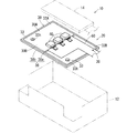
- FIG. 1 is a schematic exploded perspective view showing an electrical connection box according to the first embodiment.
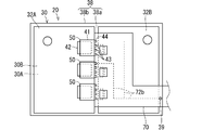
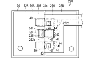
- FIG. 2 is a plan view showing the substrate structure.
- FIG. 3 is a bottom view showing the substrate structure.
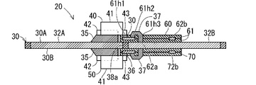
- FIG. 4 is a sectional view taken along line IV-IV of FIG.
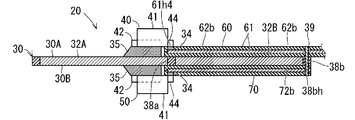
- FIG. 5 is a sectional view taken along line VV of FIG.
- FIG. 6 is a plan view showing the substrate structure according to the second embodiment.
- FIG. 7 is a bottom view showing the substrate structure.
- FIG. 8 is a plan view showing a substrate structure according to a modified example of the second embodiment.
- the substrate structure of the present disclosure is as follows.
- a base substrate including a first conductive plate and a second conductive plate, a first element connected to the first conductive plate and the second conductive plate, the first conductive plate and the second conductive plate.
- the first conductive plate and the second conductive plate are arranged along the same plane in a state of being insulated from each other, and the first conductive plate is provided with a second element connected to the first conductive plate.
- the first element and the second element may be arranged in a small region so as not to interfere with each other. Therefore, the substrate structure including the plurality of elements can be further miniaturized.
- the base substrate includes an insulating portion formed by molding the first conductive plate and the second conductive plate as inserts, and the insulating portion includes the first conductive plate and the second conductive plate.
- the first conductive plate and the second conductive plate may be kept in a state along the same plane while insulating the space between them.
- the first conductive plate and the second conductive plate are held in a state of being insulated by the insulating portion, and the first conductive plate and the second conductive plate are held along the same plane.
- the first element and the second element may be mounted so as to at least partially overlap each other in the direction along the boundary between the first conductive plate and the second conductive plate.
- the first element and the second element can be arranged in a region as small as possible.
- the first element and the second element may be dispersedly mounted on both sides of the boundary between the first conductive plate and the second conductive plate.
- the heat generated by the first element and the second element is dispersed. As a result, the heat dissipation effect is enhanced.
- a first sheet-shaped wiring member superposed on the first main surface of the base substrate and a second sheet-shaped wiring member superposed on the second main surface of the base substrate are further provided.
- the first element includes a first control terminal into which a control signal is input, and energizes and shuts off between the first conductive plate and the second conductive plate in response to a control signal to the first control terminal.
- the second element includes a second control terminal into which a control signal is input, and the first conductive plate and the second conductive plate in response to a control signal to the second control terminal. It is a second switching element that energizes and shuts off from the plate, and the first sheet-shaped wiring member includes a first linear conductor connected to the first control terminal, and the second sheet-shaped wiring member. May include a second linear conductor connected to the second control terminal.
- the first control terminal and the second control terminal can be connected to the outside by using the first sheet-shaped wiring member or the second sheet-shaped wiring member.
- the first linear conductor and the second linear conductor are electrically connected via a conductive portion in a portion of the base substrate other than the first conductive plate and the second conductive plate. May be good.
- the first control terminal and the second control terminal are easily connected to an external control board.
- the substrate structure according to the first embodiment will be described.
- the electrical junction box 10 including the substrate structure 20 will be described as an example.
- FIG. 1 is a schematic exploded perspective view showing the electrical connection box 10 according to the first embodiment.
- FIG. 2 is a plan view showing the substrate structure 20.
- FIG. 3 is a bottom view showing the substrate structure 20.
- FIG. 4 is a sectional view taken along line IV-IV of FIG.
- FIG. 5 is a sectional view taken along line VV of FIG.
- the thickness and the like of each part may be exaggerated in FIGS. 4 and 5.
- the electrical junction box 10 includes a substrate structure 20, a housing 12, and a control substrate 14.
- the housing 12 is made of resin or the like.
- the substrate structure 20 and the control substrate 14 are housed in the housing 12.
- the housing 12 is formed with a recess for exposing the external connection portion 33 of the substrate structure 20 to the outside.
- the substrate structure 20 includes a base substrate 30, a first element 40, and a second element 50.
- the base substrate 30 includes a first conductive plate 32A and a second conductive plate 32B.
- the first element 40 is connected to the first conductive plate 32A and the second conductive plate 32B.
- the second element 50 is connected to the first conductive plate 32A and the second conductive plate 32B.
- the current flows through the first conductive plate 32A, the first element 40, the second element 50, and the second conductive plate 32B.
- the direction in which the current flows may be any of the first conductive plate 32A to the second conductive plate 32B and the second conductive plate 32B to the first conductive plate 32A.
- the control board 14 is connected to the board structure 20.
- the control board 14 controls the operation of the board structure 20.
- the control board 14 controls on / off of the current flowing through the board structure 20.
- the electric junction box 10 is provided, for example, in a power supply path between a power source and various electrical components in an automobile.
- the substrate structure 20 includes a base substrate 30, a first element 40, and a second element 50.
- the base substrate 30 includes a first conductive plate 32A and a second conductive plate 32B.
- the first conductive plate 32A and the second conductive plate 32B are members formed of a metal plate or the like.
- the first conductive plate 32A and the second conductive plate 32B are sometimes called a bus bar.
- the first conductive plate 32A and the second conductive plate 32B are formed in a square plate shape.
- the first conductive plate 32A and the second conductive plate 32B function as an external path for the current flowing through the first element 40 and the second element 50.
- the first conductive plate 32A and the second conductive plate 32B are arranged along the same plane in a state of being insulated from each other.
- a straight edge portion is formed on a part of the outer periphery of the first conductive plate 32A.
- a straight edge portion is formed on a part of the outer periphery of the second conductive plate 32B.
- the straight edge portion of the first conductive plate 32A and the straight edge portion of the second conductive plate 32B are parallel to each other and face each other with a gap. Therefore, the first conductive plate 32A and the second conductive plate 32B are in a state of being insulated from each other.
- the base substrate 30 further includes an insulating portion 38.
- the insulating portion 38 is a portion formed of resin or the like.
- the insulating portion 38 is a portion formed by using the first conductive plate 32A and the second conductive plate 32B as inserts.
- the insulating portion 38 includes an insulating interposing portion 38a and an insulating holding portion 38b.
- the insulating intervening portion 38a is provided between the straight edge portion of the first conductive plate 32A and the straight edge portion of the second conductive plate 32B.
- the insulating intervening portion 38a keeps the first conductive plate 32A and the second conductive plate 32B in a state of being insulated as reliably as possible.
- the insulation holding portion 38b is provided so as to surround the outer periphery of the first conductive plate 32A and the second conductive plate 32B.
- the first conductive plate 32A and the second conductive plate 32B are surrounded by the insulating interposing portion 38a and the insulating holding portion 38b, so that the first conductive plate 32A and the second conductive plate 32B are held along the same plane. ..
- the first conductive plate 32A and the second conductive plate 32B may be kept in a state of being arranged along the same plane in a state of being insulated from each other by another configuration.
- the first conductive plate 32A and the second conductive plate 32B may be fitted into a resin frame member that has been molded in advance.
- the first conductive plate 32A and the second conductive plate 32B may be joined to a sheet-shaped member or the like. In this case, it is sufficient that a hole is formed in a portion of the sheet-shaped member on which the element is mounted.
- Holes 33h are formed in the first conductive plate 32A and the second conductive plate 32B.
- the portion of the first conductive plate 32A and the second conductive plate 32B in which the hole 33h is formed functions as an external connecting portion 33 for connecting the first conductive plate 32A and the second conductive plate 32B to an external conductive path. can do.
- the first element 40 is an element connected to the first conductive plate 32A and the second conductive plate 32B.
- the first element 40 is an element according to the application of the electrical junction box 10.
- a semiconductor switching element exemplified by a field effect transistor (hereinafter, also referred to as “FET”) is adopted.
- the first element 40 may be a resistor, a coil, or a capacitor.
- the first element 40 is an FET. More specifically, the first element 40 is, for example, a surface mount type power MOSFET.
- the first element 40 includes an element main body 41, a first terminal 42, a second terminal 43, and a third terminal 44.
- One of the first terminal 42 and the second terminal 43 functions as a source electrode, and the other functions as a drain electrode.
- the first terminal 42 is the drain electrode and the second terminal 43 is the source electrode.
- the third terminal 44 is, for example, a first control terminal into which a control signal is input.
- the first element 40 energizes and shuts off between the first conductive plate 32A and the second conductive plate 32B.
- the third terminal 44 is a gate electrode.
- the element body 41 is formed, for example, in a flat rectangular parallelepiped shape.
- the first terminal 42 is provided so as to project from the bottom of the element main body 41 to one side.
- the second terminal 43 and the third terminal 44 are provided so as to project from the other side of the element main body 41.
- a plurality of second terminals 43 are provided.
- the first element 40 is connected to the first conductive plate 32A and the second conductive plate 32B. Further, the first element 40 is mounted on the first main surface 30A of the base substrate 30. In the present embodiment, the element main body 41 of the first element 40 is located on the first conductive plate 32A.
- the first terminal 42 is electrically connected to the first conductive plate 32A on the first conductive plate 32A.
- the first terminal 42 is connected to the first conductive plate 32A by the solder 35 (see FIG. 4).
- the solder connection points of the two parts may be fixed in a state where the two parts are electrically connected. For example, the two parts may be connected by a conductive adhesive.
- the second terminal 43 is connected to the second conductive plate 32B.
- the second terminal 43 extends from the element main body 41 on the first conductive plate 32A to the second conductive plate 32B side.
- the second terminal 43 is located on the insulating interposition portion 38a.
- the second terminal 43 is electrically connected to the second conductive plate 32B via the first sheet-shaped wiring member 60.
- the first sheet-shaped wiring member 60 is a member in which the conductor is covered with an insulating member and formed in a sheet shape.
- the first sheet-shaped wiring member 60 is a flexible printed circuit board (FPC) is exemplified. That is, the first sheet-shaped wiring member 60 is a sheet-shaped member in which a conductor formed of a metal foil (copper foil) or the like is sandwiched between a pair of resin films 61.
- the first sheet-shaped wiring member 60 is formed in a sheet shape extending from the insulating interposing portion 38a toward the second conductive plate 32B on the first main surface of the base substrate 30.
- the first sheet-shaped wiring member 60 includes a relay conductor 62a and a first linear conductor 62b as conductors.
- the relay conductor 62a is formed so as to extend from the lower region of the second terminal 43 of the first element 40 toward the second conductive plate 32B.
- the relay conductor 62a is formed in a rectangular region extending from a region extending downwardly of the plurality of second terminals 43 toward the second conductive plate 32B.
- the resin film 61 on the side of the second terminal 43 is formed with an opening 61h1 that opens in a region directly below the second terminal 43.
- the resin film 61 on the side of the second terminal 43 is formed with an opening 61h2 that opens in a region closer to the second conductive plate 32B than the opening 61h1.
- the relay conductor 62a can be exposed.
- first sheet-shaped wiring member 60 is formed with a through hole 61h3 that penetrates in a region away from the opening 61h2.
- the second conductive plate 32B can be exposed in the through hole 61h3.
- the second terminal 43 is connected to the relay conductor 62a exposed by the opening 61h1 by the solder 36 in a state where the first sheet-shaped wiring member 60 is superposed on the first main surface 30A of the base substrate 30 (FIG. 4). reference). Further, the relay conductor 62a exposed by the opening 61h2 and the second conductive plate 32B exposed by the through hole 61h3 are connected by the solder 37 (see FIG. 4). Therefore, the second terminal 43 is electrically connected to the second conductive plate 32B via the solder 36, the relay conductor 62a, and the solder 37. Therefore, the first element 40 is mounted on the first main surface 30A of the base substrate 30 in a state of being connected to the first conductive plate 32A and the second conductive plate 32B. The second terminal 43 may be directly connected to the second conductive plate 32B by solder or the like.
- the third terminal 44 is connected to the first linear conductor 62b.
- the first linear conductor 62b is a linear conductor extending from the lower region of the third terminal 44 toward any part of the outer circumference of the base substrate 30.
- the resin film 61 on the third terminal 44 side is formed with an opening 61h4 that opens in a region directly below the third terminal 44.
- the third terminal 44 is connected to the first linear conductor 62b exposed by the opening 61h4 by a solder 34 (see FIG. 5).
- the first sheet-shaped wiring member 60 may extend outward from the base board 30 and be connected to the control board 14.
- the first linear conductor 62b may extend outward of the first sheet-shaped wiring member 60 and be connected to the control board 14.
- the control signal output from the control board 14 is given to the third terminal 44 via the first linear conductor 62b.
- the second element 50 has the same configuration as the first element 40. Each part of the second element 50 is designated by the same reference numeral as that of the first element 40, and redundant description is omitted.
- the second element 50 is connected to the first conductive plate 32A and the second conductive plate 32B. Further, the second element 50 is mounted on the second main surface 30B of the base substrate 30.
- the configuration for mounting the second element 50 on the base substrate 30 is the same as the configuration for mounting the first element 40 on the base substrate 30, except for the following configuration. The difference is that the second element 50 is mounted on the second main surface 30B on the side opposite to the first main surface 30A with respect to the base substrate 30, and the second element 50 is replaced with the first sheet-shaped wiring member 60. The point is that the sheet-shaped wiring member 70 is used.
- the side opposite to the first main surface 30A with respect to the base substrate 30 means the side opposite to the thickness direction of the base substrate 30.
- the configuration for mounting the second element 50 on the base substrate 30 the same components as the configuration for mounting the first element 40 on the base substrate 30 are designated by the same reference numerals, and redundant description is omitted. Will be done.
- the position where the second element 50 is mounted is a region opposite to the region where the first element 40 is mounted in the thickness direction of the base substrate 30. Therefore, when the substrate structure 20 is viewed in a plane in a direction along the thickness direction thereof, the first element 40 and the second element 50 are arranged in a region where they overlap each other.
- first element 40 and the second element 50 are arranged in the same region in a plan view of the substrate structure 20. Even if the first element 40 and the second element 50 are mounted at positions displaced from each other in the direction along the boundary between the first conductive plate 32A and the second conductive plate 32B (here, the insulating interposition portion 38a). Good. In this case, the first element 40 and the second element 50 partially overlap each other in the direction along the boundary between the first conductive plate 32A and the second conductive plate 32B (here, the insulating interposition portion 38a). It is preferable to have.
- first element 40 and the second element 50 may be mounted on the first conductive plate 32A side, and the other may be mounted on the second conductive plate 32B side. Also in this case, it is preferable that the first element 40 and the second element 50 are mounted so as to at least partially overlap each other in the direction along the boundary between the first conductive plate 32A and the second conductive plate 32B. .. An example of the latter will be described in Embodiment 2.
- the second sheet-shaped wiring member 70 differs from the first sheet-shaped wiring member 60 in the following points.
- the second sheet-shaped wiring member 70 is superposed on the second main surface 30B on the side opposite to the first main surface 30A with respect to the base substrate 30.
- a portion of the first sheet-shaped wiring member 60 that extends outward from the base substrate 30 and is connected to the control substrate 14 is omitted.
- the second linear conductor 72b corresponding to the first linear conductor 62b is connected to the third terminal 44 of the second element 50.
- the second linear conductor 72b extends from the connection portion with respect to the third terminal 44 and reaches the insulation holding portion 38b.
- the third terminal of the second element 50 is an example of the second control terminal.
- the same components as those of the first sheet-shaped wiring member 60 are designated by the same reference numerals, and duplicate explanations are omitted.
- the first linear conductor 62b and the second linear conductor 72b are electrically connected via the conductive portion 39 in the portion of the base substrate 30 other than the first conductive plate 32A and the second conductive plate 32B.
- the first linear conductor 62b and the second linear conductor 72b extend along the same path.
- a portion of the first linear conductor 62b that passes through the insulation holding portion 38b and a portion of the second linear conductor 72b that reaches the insulation holding portion 38b are connected via a conductive portion 39.
- the conductive portion 39 is a conductive member that penetrates the insulation holding portion 38b and connects the first linear conductor 62b and the second linear conductor 72b.
- a through hole 38bh is formed in the insulation holding portion 38b. Further, a through hole is formed in a portion of the first linear conductor 62b and the second linear conductor 72b corresponding to the through hole 38bh, and the first linear conductor 62b and the second linear conductor are formed on the peripheral edge thereof.
- the conductor 72b is formed so as to be exposed. Then, solder is provided so as to penetrate the through hole 38bh on the inner peripheral surface or the entire inside of the through hole 38bh, and is soldered to the exposed portion of the first linear conductor 62b and the second linear conductor 72b. ..
- the conductive portion 39 formed in this way penetrates the through hole 38bh and electrically connects the first linear conductor 62b and the second linear conductor 72b.
- the case where the first element 40 is a plurality and the second element 50 is a plurality is exemplified.
- the plurality of first elements 40 are mounted side by side along the boundary between the first conductive plate 32A and the second conductive plate 32B.
- the first linear conductor 62b branches and extends toward the third terminal 44 of each of the plurality of first elements 40.
- the plurality of second elements 50 are mounted side by side along the boundary between the first conductive plate 32A and the second conductive plate 32B.
- the second linear conductor 72b branches and extends toward the third terminal 44 of each of the plurality of first elements 40.
- the plurality of first elements 40 and the plurality of second elements 50 are all located on the first conductive plate 32A side and mounted on the base substrate 30. Further, the distance between the plurality of first elements 40 and the distance between the plurality of second elements 50 are also the same. When the base substrate 30 is viewed in a plan view, the plurality of first elements 40 and the plurality of second elements 50 are in a positional relationship in which they overlap each other in the same region.
- the number of the first element 40 and the second element 50 is arbitrary.
- the first element 40 is mounted on the first main surface 30A with respect to the base substrate 30, and the second element 50 is mounted on the second main surface 30B with respect to the base substrate 30. Is implemented in. Therefore, the first element 40 and the second element 50 can be mounted in a region as small as possible so as not to interfere with each other. Therefore, the substrate structure 20 including the plurality of elements 40 and 50 can be further miniaturized.
- a plurality of elements connecting the first conductive plate and the second conductive plate will be mounted along the boundary between the first conductive plate and the second conductive plate. Assuming that a plurality of elements are mounted only on one main surface of the base substrate, since the plurality of elements are lined up along the boundary, the mounting area of the plurality of elements becomes large. Therefore, it is preferable that the first element 40 and the second element 50 are mounted so as to overlap each other in the direction along the boundary between the first conductive plate 32A and the second conductive plate 32B. As a result, the mounting regions of the plurality of elements 40 and 50 become smaller in the direction along the boundary between the first conductive plate 32A and the second conductive plate 32B.
- the first element 40 does not need to overlap with respect to all the plurality of second elements 50 in the direction along the boundary.
- the first element 40 may overlap a part of the plurality of second elements 50 in the direction along the boundary.
- the second element 50 does not need to overlap with respect to all the plurality of first elements 40 in the direction along the boundary.
- the second element 50 may overlap a part of the plurality of first elements 40 in the direction along the boundary.
- another element that does not overlap in the direction along the boundary with respect to the element on the opposite side may be mounted on the first main surface 30A or the second main surface 30B of the base substrate 30.
- first sheet-shaped wiring member 60 is superposed on the first main surface 30A of the base substrate 30.
- the first linear conductor 62b of the first sheet-shaped wiring member 60 is connected to the third terminal 44, which is the first control terminal of the first element 40.
- the second sheet-shaped wiring member 70 is superposed on the second main surface 30B of the base substrate 30.
- the second linear conductor 72b of the second sheet-shaped wiring member 70 is connected to the third terminal 44, which is the second control terminal of the second element 50. Therefore, the elements 40 and 50 mounted on both sides of the base board 30 are connected to the external control board 14 and the like via the first sheet-shaped wiring member 60 and the second sheet-shaped wiring member 70.
- the first sheet-shaped wiring member 60 and the second sheet-shaped wiring member 70 are electrically connected via the conductive portion 39. Therefore, for example, the first sheet-shaped wiring member 60 may be pulled out of the base substrate 30 and connected to the control substrate 14.
- the third terminal 44 which is the first control terminal of the first element 40
- the third terminal 44 which is the second control terminal of the second element 50
- FIG. 6 is a plan view showing the substrate structure 120.
- FIG. 7 is a bottom view of the substrate structure 120 as viewed from the side opposite to FIG.
- the same reference numerals are given to the components as described in the substrate structure 20 in the first embodiment, and the description thereof is omitted.
- the first element 40 is mounted on the first conductive plate 32A side.
- the mounting configuration of the first element 40 on the base substrate 30 is the same as that of the first embodiment.
- the difference between the substrate structure 120 and the substrate structure 20 is the mounting position of the second element 50 and the configuration for mounting the second element 50.
- the second element 50 is mounted on the second conductive plate 32B side. More specifically, the element main body 41 of the second element 50 is located on the second conductive plate 32B side.
- the first element 40 is provided on the first main surface 30A side with respect to the base substrate 30, and the second element 50 is provided on the second main surface 30B side on the opposite side.
- the first terminal 42 is located closer to the first conductive plate 32A with respect to the element main body 41, and the second terminal 43 and the third terminal 44 are the element main body 41. It is located closer to the second conductive plate 32B.
- a second sheet-shaped wiring member 170 is provided on the second main surface 30B side with respect to the base substrate 30. Like the first sheet-shaped wiring member 60, the second sheet-shaped wiring member 170 is provided with a second linear conductor (corresponding to the first linear conductor) as a conductor. Then, the second element 50 is mounted on the second sheet-shaped wiring member 170 in a state where the second sheet-shaped wiring member 170 is superposed on the second main surface 30B side of the second conductive plate 32B. At this time, the second terminal 43 is soldered to the second conductive plate 32B through the through hole of the second sheet-shaped wiring member 170. Further, the third terminal 44 is soldered to the second linear conductor of the second sheet-shaped wiring member 170. A control signal is given to the third terminal 44 via the second linear conductor.
- a second linear conductor corresponding to the first linear conductor
- Both the first sheet-shaped wiring member 60 and the second sheet-shaped wiring member 170 may be pulled out with respect to the base substrate 30.
- the first linear conductor of the first sheet-shaped wiring member 60 and the second linear conductor of the second sheet-shaped wiring member 170 are connected at any position on the base substrate 30, and the first sheet-shaped wiring member 60 And one of the second sheet-shaped wiring member 170 may be pulled out with respect to the base substrate 30.
- the first terminal 42 of the second element 50 extends from the second conductive plate 32B toward the insulating interposition portion 38a. At least a part of the second sheet-shaped wiring member 170 extends from the first terminal 42 toward the first conductive plate 32A as an extending portion 171. A relay conductor similar to the relay conductor 62a is provided in the extending portion 171. Similar to connecting the second terminal 43 to the second conductive plate 32B in the first embodiment, the first terminal 42 is connected to the relay conductor by solder, and the relay conductor is soldered to the first conductive plate 32A. Connected by 135. As a result, the first terminal 42 is electrically connected to the first conductive plate 32A.
- the first element 40 is mounted on the first conductive plate 32A side
- the second element 50 is mounted on the second conductive plate 32B side. That is, the second embodiment is an example in which the first element 40 and the second element 50 are dispersed and mounted on both sides of the boundary between the first conductive plate 32A and the second conductive plate 32B.
- the same effects as those of the first embodiment can be obtained. Further, since the first element 40 and the second element 50 are dispersed on both sides of the boundary, the heat generated by the first element 40 and the second element 50 is dispersed. Therefore, heat is efficiently dissipated from the substrate structure 120.
- the heat radiating member 190 such as the heat radiating fin is provided only on one side of the substrate structure 120, heat radiating is efficiently performed.
- the heat radiating member 190 is provided on one surface side of the substrate structure 120 (the first main surface 30A side of the base substrate 30).
- FIGS. 6 and 7 an example of the arrangement region of the heat radiating member 190 is illustrated by a two-dot chain line.
- the heat radiating member 190 may be arranged in direct contact with or close to the first element 40 at the portion where the first element 40 is mounted. Therefore, the heat generated by the first element 40 is efficiently dissipated by the heat radiating member 190.
- the heat radiating member 190 may be directly in contact with or close to the base substrate 30 from the side opposite to the second element 50.
- the heat generated by the second element 50 is transferred to the heat radiating member 190 via the base substrate 30 (here, the second conductive plate 32B), and is efficiently radiated. Therefore, the heat generated by the first element 40 and the second element 50 can be efficiently dissipated through the heat radiating member 190.
- FIG. 8 is a plan view showing the substrate structure 220 according to the modified example of the second embodiment.
- a plurality of (three in this case) first elements 40 are alternately mounted on the first conductive plate 32A side and the second conductive plate 32B side. That is, the plurality of first elements 40 are arranged so as to line up in the extending direction of the boundary between the first conductive plate 32A and the second conductive plate 32B.
- the odd-numbered first element 40 is mounted on the first conductive plate 32A side from one side to the other in the extending direction of the boundary.
- the even-numbered second element 50 is a second conductive plate. It is mounted on the 32B side.
- the configuration in which the odd-numbered first element 40 is mounted on the base substrate 30 and the configuration in which the first sheet-shaped wiring member 260 (corresponding to the first sheet-shaped wiring member 60) is connected are the same as in the first embodiment.
- the even-numbered first element 40 is mounted on the first sheet-shaped wiring member 260 on the base substrate 30 in the same posture as the odd-numbered first element 40.
- the second terminal 43 of the even-numbered first element 40 is soldered to the second conductive plate 32B through the through hole of the first sheet-shaped wiring member 260.
- the third terminal 44 of the even-numbered first element 40 is soldered to the first linear conductor 262b of the first sheet-shaped wiring member 260.
- the first terminal 42 of the even-numbered first element 40 extends from the second conductive plate 32B toward the insulating interposition portion 38a. At least a part of the first sheet-shaped wiring member 260 extends from the first terminal 42 toward the first conductive plate 32A as an extending portion 261.
- a relay conductor 262a similar to the relay conductor 62a is provided in the extending portion 261.
- the first terminal 42 is connected to the relay conductor 262a by soldering, and the relay conductor 262a is soldered to the first conductive plate 32A. Connected by 235. As a result, the first terminal 42 is electrically connected to the first conductive plate 32A.
- a plurality of (three in this case) second elements 50 are alternately mounted on the first conductive plate 32A side and the second conductive plate 32B side.
- the mounting position of the second element 50 with respect to the first conductive plate 32A and the second conductive plate 32B is opposite to the mounting position of the first element 40 with reference to the above boundary. That is, the plurality of second elements 50 are arranged so as to line up in the extending direction of the boundary between the first conductive plate 32A and the second conductive plate 32B.
- the odd-numbered second element 50 is mounted on the second conductive plate 32B side from one side to the other in the extending direction of the boundary.
- the even-numbered second element 50 is the first conductive plate 32A. It is implemented on the side.
- the first terminal 42 is located closer to the first conductive plate 32A with respect to the element main body 41, and the second terminal 43 and the third terminal 44 are the element main body 41. It is located closer to the second conductive plate 32B.
- the configuration in which the odd-numbered second element 50 is connected to the first conductive plate 32A, the second conductive plate 32B, and the second sheet-shaped wiring member (corresponding to the second sheet-shaped wiring member 70) is the even-numbered first element. 40 is the same as the configuration in which the first conductive plate 32A, the second conductive plate 32B, and the first sheet-shaped wiring member 260 are connected.
- the configuration in which the even-numbered second element 50 is connected to the first conductive plate 32A, the second conductive plate 32B, and the second sheet-shaped wiring member (existing on the back side of the first sheet-shaped wiring member) is the odd-numbered first.
- the element 40 has the same configuration as the first conductive plate 32A, the second conductive plate 32B, and the first sheet-shaped wiring member 260.
- Both the first sheet-shaped wiring member 260 and the second sheet-shaped wiring member may be pulled out with respect to the base substrate 30.
- the first linear conductor of the first sheet-shaped wiring member and the second linear conductor of the second sheet-shaped wiring member are connected at any position on the base substrate 30, and the first sheet-shaped wiring member and the second are connected.
- One of the sheet-shaped wiring members may be pulled out with respect to the base substrate 30.
Abstract
The purpose of the present disclosure is to further reduce the size of a board structure provided with a plurality of elements. This board structure is provided with: a base board including a first conductive plate and a second conductive plate; a first element connected to the first conductive plate and the second conducive plate; and a second element connected to the first conductive plate and the second conducive plate, wherein in the base board, the first conductive plate and the second conducive plate are disposed along the same plane in a state of being insulated from each other, the first element is mounted on a first main surface of the base board, and the second element is mounted on a second main surface on the reverse side from the first main surface with respect to the base board.
Description
本開示は、基板構造体に関する。
This disclosure relates to a substrate structure.
特許文献1は、複数本のバスバと、半導体スイッチング素子と、制御回路基板とを備えた回路構成体を開示している。バスバは略同一平面上に並んだ状態で制御回路基板の表面に接着されている。半導体スイッチング素子はバスバと制御回路基板の双方に実装されている。
Patent Document 1 discloses a circuit configuration including a plurality of bus bars, a semiconductor switching element, and a control circuit board. The bus bars are adhered to the surface of the control circuit board while being lined up on substantially the same plane. Semiconductor switching elements are mounted on both the bus bar and the control circuit board.
特許文献2は、一対のバスバと、一対のバスバ上に実装されて当該一対のバスバ間の通電及び遮断を行う遮断部とを備えた電気接続箱を開示している。
Patent Document 2 discloses an electric junction box provided with a pair of bus bars and a blocking unit mounted on the pair of bus bars to energize and shut off the pair of bus bars.
特許文献1及び2においては、複数の半導体スイッチング素子が、同一平面状に並んだバスバの一方主面側に実装されている。ここで、バスバと、バスバに接続される複数の素子とを備える基板構造体をさらに小型化することが要請されている。
In Patent Documents 1 and 2, a plurality of semiconductor switching elements are mounted on one main surface side of a bus bar arranged in the same plane. Here, it is required to further reduce the size of the substrate structure including the bus bar and a plurality of elements connected to the bus bar.
そこで、本開示は、複数の素子を備える基板構造体をさらに小型化することを目的とする。
Therefore, the purpose of the present disclosure is to further reduce the size of the substrate structure including a plurality of elements.
本開示の基板構造体は、第1導電板と第2導電板とを含むベース基板と、前記第1導電板及び前記第2導電板に接続された第1素子と、前記第1導電板及び前記第2導電板に接続された第2素子と、を備え、前記ベース基板において、前記第1導電板と前記第2導電板とは互いに絶縁された状態で同一平面に沿って配設されており、前記第1素子が前記ベース基板の第1主面に実装され、前記第2素子が前記ベース基板に対して前記第1主面とは反対側の第2主面に実装されている、基板構造体である。
The substrate structure of the present disclosure includes a base substrate including a first conductive plate and a second conductive plate, a first element connected to the first conductive plate and the second conductive plate, the first conductive plate, and the first conductive plate. A second element connected to the second conductive plate is provided, and the first conductive plate and the second conductive plate are arranged along the same plane in a state of being insulated from each other in the base substrate. The first element is mounted on the first main surface of the base substrate, and the second element is mounted on the second main surface of the base substrate opposite to the first main surface. It is a substrate structure.
本開示によれば、複数の素子を備える基板構造体をさらに小型化することができる。
According to the present disclosure, a substrate structure including a plurality of elements can be further miniaturized.
[本開示の実施形態の説明]
最初に本開示の実施態様を列記して説明する。 [Explanation of Embodiments of the present disclosure]
First, embodiments of the present disclosure will be listed and described.
最初に本開示の実施態様を列記して説明する。 [Explanation of Embodiments of the present disclosure]
First, embodiments of the present disclosure will be listed and described.
本開示の基板構造体は、次の通りである。
The substrate structure of the present disclosure is as follows.
(1)第1導電板と第2導電板とを含むベース基板と、前記第1導電板及び前記第2導電板に接続された第1素子と、前記第1導電板及び前記第2導電板に接続された第2素子と、を備え、前記ベース基板において、前記第1導電板と前記第2導電板とは互いに絶縁された状態で同一平面に沿って配設されており、前記第1素子が前記ベース基板の第1主面に実装され、前記第2素子が前記ベース基板に対して前記第1主面とは反対側の第2主面に実装されている、基板構造体である。第1素子と第2素子とが互いに干渉することなくなるべく小さい領域に配設され得る。このため、複数の素子を備える基板構造体をさらに小型化することができる。
(1) A base substrate including a first conductive plate and a second conductive plate, a first element connected to the first conductive plate and the second conductive plate, the first conductive plate and the second conductive plate. In the base substrate, the first conductive plate and the second conductive plate are arranged along the same plane in a state of being insulated from each other, and the first conductive plate is provided with a second element connected to the first conductive plate. A substrate structure in which an element is mounted on a first main surface of the base substrate, and the second element is mounted on a second main surface of the base substrate opposite to the first main surface. .. The first element and the second element may be arranged in a small region so as not to interfere with each other. Therefore, the substrate structure including the plurality of elements can be further miniaturized.
(2)前記ベース基板は、前記第1導電板と前記第2導電板とをインサート物として金型成形された絶縁部を含み、前記絶縁部は、前記第1導電板と前記第2導電板との間を絶縁すると共に、前記第1導電板と前記第2導電板とを同一平面に沿った状態に保持してもよい。絶縁部によって、第1導電板と第2導電板とを絶縁した状態で、第1導電板と第2導電板とが同一平面に沿った状態で保持される。
(2) The base substrate includes an insulating portion formed by molding the first conductive plate and the second conductive plate as inserts, and the insulating portion includes the first conductive plate and the second conductive plate. The first conductive plate and the second conductive plate may be kept in a state along the same plane while insulating the space between them. The first conductive plate and the second conductive plate are held in a state of being insulated by the insulating portion, and the first conductive plate and the second conductive plate are held along the same plane.
(3)前記第1素子と前記第2素子とは、前記第1導電板と前記第2導電板との境界に沿った方向において少なくとも部分的に重なるように実装されていてもよい。第1素子と第2素子とがなるべく小さい領域に配設され得る。
(3) The first element and the second element may be mounted so as to at least partially overlap each other in the direction along the boundary between the first conductive plate and the second conductive plate. The first element and the second element can be arranged in a region as small as possible.
(4)前記第1素子と前記第2素子とは、前記第1導電板と前記第2導電板との境界の両側に分散して実装されていてもよい。第1素子と第2素子で生じた熱が分散される。これにより、放熱効果が高められる。
(4) The first element and the second element may be dispersedly mounted on both sides of the boundary between the first conductive plate and the second conductive plate. The heat generated by the first element and the second element is dispersed. As a result, the heat dissipation effect is enhanced.
(5)前記ベース基板の前記第1主面に重ね合された第1シート状配線部材と、前記ベース基板の前記第2主面に重ね合された第2シート状配線部材と、をさらに備え、前記第1素子は、制御信号が入力される第1制御端子を含み、前記第1制御端子への制御信号に応じて前記第1導電板と前記第2導電板との間で通電及び遮断を行う第1スイッチング素子であり、前記第2素子は、制御信号が入力される第2制御端子を含み、前記第2制御端子への制御信号に応じて前記第1導電板と前記第2導電板との間で通電及び遮断を行う第2スイッチング素子であり、前記第1シート状配線部材は、前記第1制御端子に接続された第1線状導体を含み、前記第2シート状配線部材は、前記第2制御端子に接続された第2線状導体を含むものであってもよい。ベース基板の両面において、第1制御端子及び第2制御端子が、第1シート状配線部材又は第2シート状配線部材を利用して、外部に接続され得る。
(5) A first sheet-shaped wiring member superposed on the first main surface of the base substrate and a second sheet-shaped wiring member superposed on the second main surface of the base substrate are further provided. The first element includes a first control terminal into which a control signal is input, and energizes and shuts off between the first conductive plate and the second conductive plate in response to a control signal to the first control terminal. The second element includes a second control terminal into which a control signal is input, and the first conductive plate and the second conductive plate in response to a control signal to the second control terminal. It is a second switching element that energizes and shuts off from the plate, and the first sheet-shaped wiring member includes a first linear conductor connected to the first control terminal, and the second sheet-shaped wiring member. May include a second linear conductor connected to the second control terminal. On both sides of the base substrate, the first control terminal and the second control terminal can be connected to the outside by using the first sheet-shaped wiring member or the second sheet-shaped wiring member.
(6)前記第1線状導体と前記第2線状導体とが前記ベース基板のうち前記第1導電板及び前記第2導電板を除く部分で導通部を介して電気的に接続されていてもよい。第1制御端子及び第2制御端子が、外部の制御基板に容易に接続される。
(6) The first linear conductor and the second linear conductor are electrically connected via a conductive portion in a portion of the base substrate other than the first conductive plate and the second conductive plate. May be good. The first control terminal and the second control terminal are easily connected to an external control board.
[本開示の実施形態の詳細]
本開示の基板構造体の具体例を、以下に図面を参照しつつ説明する。なお、本開示はこれらの例示に限定されるものではなく、請求の範囲によって示され、請求の範囲と均等の意味および範囲内でのすべての変更が含まれることが意図される。 [Details of Embodiments of the present disclosure]
Specific examples of the substrate structure of the present disclosure will be described below with reference to the drawings. It should be noted that the present disclosure is not limited to these examples, but is indicated by the scope of claims and is intended to include all modifications within the meaning and scope equivalent to the scope of claims.
[実施形態1]
以下、実施形態1に係る基板構造体について説明する。実施形態1では、基板構造体20を備える電気接続箱10が例として説明される。 [Embodiment 1]
Hereinafter, the substrate structure according to the first embodiment will be described. In the first embodiment, theelectrical junction box 10 including the substrate structure 20 will be described as an example.
以下、実施形態1に係る基板構造体について説明する。実施形態1では、基板構造体20を備える電気接続箱10が例として説明される。 [Embodiment 1]
Hereinafter, the substrate structure according to the first embodiment will be described. In the first embodiment, the
図1は実施形態1に係る電気接続箱10を示す概略分解斜視図である。図2は基板構造体20を示す平面図である。図3は基板構造体20を示す底面図である。図4は図2のIV-IV線断面図である。図5は図2のV-V線断面図である。なお、説明の便宜上、図4及び図5において各部の厚み等が誇張して描かれている場合がある。
FIG. 1 is a schematic exploded perspective view showing the electrical connection box 10 according to the first embodiment. FIG. 2 is a plan view showing the substrate structure 20. FIG. 3 is a bottom view showing the substrate structure 20. FIG. 4 is a sectional view taken along line IV-IV of FIG. FIG. 5 is a sectional view taken along line VV of FIG. For convenience of explanation, the thickness and the like of each part may be exaggerated in FIGS. 4 and 5.
<電気接続箱の全体構成>
電気接続箱10は、基板構造体20と、筐体12と、制御基板14とを備える。 <Overall configuration of electrical junction box>
Theelectrical junction box 10 includes a substrate structure 20, a housing 12, and a control substrate 14.
電気接続箱10は、基板構造体20と、筐体12と、制御基板14とを備える。 <Overall configuration of electrical junction box>
The
筐体12は、樹脂等で形成されている。筐体12内には、基板構造体20及び制御基板14が収容される。筐体12には、基板構造体20の外部接続部33を外部に露出させるための凹部が形成されている。
The housing 12 is made of resin or the like. The substrate structure 20 and the control substrate 14 are housed in the housing 12. The housing 12 is formed with a recess for exposing the external connection portion 33 of the substrate structure 20 to the outside.
基板構造体20は、ベース基板30と、第1素子40と、第2素子50とを備える。ベース基板30は、第1導電板32Aと、第2導電板32Bとを備える。第1素子40は、第1導電板32Aと第2導電板32Bとに接続される。第2素子50は、第1導電板32Aと第2導電板32Bとに接続される。本基板構造体20において、電流は、第1導電板32Aと、第1素子40及び第2素子50と、第2導電板32Bを経て流れる。電流が流れる方向は、第1導電板32Aから第2導電板32B、第2導電板32Bから第1導電板32Aのいずれであってもよい。
The substrate structure 20 includes a base substrate 30, a first element 40, and a second element 50. The base substrate 30 includes a first conductive plate 32A and a second conductive plate 32B. The first element 40 is connected to the first conductive plate 32A and the second conductive plate 32B. The second element 50 is connected to the first conductive plate 32A and the second conductive plate 32B. In the substrate structure 20, the current flows through the first conductive plate 32A, the first element 40, the second element 50, and the second conductive plate 32B. The direction in which the current flows may be any of the first conductive plate 32A to the second conductive plate 32B and the second conductive plate 32B to the first conductive plate 32A.
制御基板14は、基板構造体20に接続されている。制御基板14は、基板構造体20の動作を制御する。例えば、制御基板14は、基板構造体20を流れる電流をオンオフ制御する。
The control board 14 is connected to the board structure 20. The control board 14 controls the operation of the board structure 20. For example, the control board 14 controls on / off of the current flowing through the board structure 20.
本電気接続箱10は、例えば、自動車において、電源と、各種電装品との間の電力供給経路に設けられる。
The electric junction box 10 is provided, for example, in a power supply path between a power source and various electrical components in an automobile.
<基板構造体>
基板構造体20は、ベース基板30と、第1素子40と、第2素子50とを備える。 <Board structure>
Thesubstrate structure 20 includes a base substrate 30, a first element 40, and a second element 50.
基板構造体20は、ベース基板30と、第1素子40と、第2素子50とを備える。 <Board structure>
The
ベース基板30は、第1導電板32Aと第2導電板32Bとを備える。第1導電板32A及び第2導電板32Bは、金属板等によって形成された部材である。第1導電板32A及び第2導電板32Bは、バスバと呼ばれることもある。ここでは、一例として、第1導電板32A及び第2導電板32Bは、方形板状に形成されている。第1導電板32A及び第2導電板32Bは、第1素子40及び第2素子50を流れる電流の外部経路として機能する。
The base substrate 30 includes a first conductive plate 32A and a second conductive plate 32B. The first conductive plate 32A and the second conductive plate 32B are members formed of a metal plate or the like. The first conductive plate 32A and the second conductive plate 32B are sometimes called a bus bar. Here, as an example, the first conductive plate 32A and the second conductive plate 32B are formed in a square plate shape. The first conductive plate 32A and the second conductive plate 32B function as an external path for the current flowing through the first element 40 and the second element 50.
ベース基板30において、第1導電板32Aと第2導電板32Bとは互いに絶縁された状態で同一平面に沿って配設される。ここでは、第1導電板32Aにおける外周囲の一部に、直線縁部が形成されている。また、第2導電板32Bにおける外周囲の一部に直線縁部が形成されている。第1導電板32Aの直線縁部と第2導電板32Bの直線縁部とが互いに平行状態で間隔をあけて対向している。このため、第1導電板32Aと第2導電板32Bとは互いに絶縁された状態となっている。
In the base substrate 30, the first conductive plate 32A and the second conductive plate 32B are arranged along the same plane in a state of being insulated from each other. Here, a straight edge portion is formed on a part of the outer periphery of the first conductive plate 32A. Further, a straight edge portion is formed on a part of the outer periphery of the second conductive plate 32B. The straight edge portion of the first conductive plate 32A and the straight edge portion of the second conductive plate 32B are parallel to each other and face each other with a gap. Therefore, the first conductive plate 32A and the second conductive plate 32B are in a state of being insulated from each other.
ここでは、ベース基板30は、絶縁部38をさらに備える。絶縁部38は、樹脂等によって形成された部分である。絶縁部38は、第1導電板32Aと第2導電板32Bをインサート物として金型成形された部分である。
Here, the base substrate 30 further includes an insulating portion 38. The insulating portion 38 is a portion formed of resin or the like. The insulating portion 38 is a portion formed by using the first conductive plate 32A and the second conductive plate 32B as inserts.
より具体的には、絶縁部38は、絶縁介在部38aと、絶縁保持部38bとを備える。絶縁介在部38aは、第1導電板32Aの直線縁部と第2導電板32Bの直線縁部との間に設けられている。絶縁介在部38aによって、第1導電板32Aと第2導電板32Bとがなるべく確実に絶縁された状態に保たれる。絶縁保持部38bは、第1導電板32A及び第2導電板32Bの外周囲を囲むように設けられている。第1導電板32Aと第2導電板32Bとが絶縁介在部38a及び絶縁保持部38bによって囲まれることで、第1導電板32Aと第2導電板32Bとが同一平面に沿うように保持される。
More specifically, the insulating portion 38 includes an insulating interposing portion 38a and an insulating holding portion 38b. The insulating intervening portion 38a is provided between the straight edge portion of the first conductive plate 32A and the straight edge portion of the second conductive plate 32B. The insulating intervening portion 38a keeps the first conductive plate 32A and the second conductive plate 32B in a state of being insulated as reliably as possible. The insulation holding portion 38b is provided so as to surround the outer periphery of the first conductive plate 32A and the second conductive plate 32B. The first conductive plate 32A and the second conductive plate 32B are surrounded by the insulating interposing portion 38a and the insulating holding portion 38b, so that the first conductive plate 32A and the second conductive plate 32B are held along the same plane. ..
第1導電板32Aと第2導電板32Bとは、他の構成によって、互いに絶縁された状態で同一平面に沿って配設された状態に保たれてもよい。例えば、予め金型成形された樹脂製の枠部材に、第1導電板32Aと第2導電板32Bとが嵌め込まれる構成であってもよい。また、第1導電板32Aと第2導電板32Bとが、シート状の部材に接合等される構成であってもよい。この場合、シート状の部材のうち素子が実装される部分に孔が形成されていればよい。
The first conductive plate 32A and the second conductive plate 32B may be kept in a state of being arranged along the same plane in a state of being insulated from each other by another configuration. For example, the first conductive plate 32A and the second conductive plate 32B may be fitted into a resin frame member that has been molded in advance. Further, the first conductive plate 32A and the second conductive plate 32B may be joined to a sheet-shaped member or the like. In this case, it is sufficient that a hole is formed in a portion of the sheet-shaped member on which the element is mounted.
第1導電板32Aと第2導電板32Bには、孔33hが形成されている。第1導電板32Aと第2導電板32Bのうち孔33hが形成された部分は、第1導電板32Aと第2導電板32Bとを外部の導電路に接続するための外部接続部33として機能することができる。
Holes 33h are formed in the first conductive plate 32A and the second conductive plate 32B. The portion of the first conductive plate 32A and the second conductive plate 32B in which the hole 33h is formed functions as an external connecting portion 33 for connecting the first conductive plate 32A and the second conductive plate 32B to an external conductive path. can do.
第1素子40は、第1導電板32A及び第2導電板32Bに接続された素子である。第1素子40は電気接続箱10の用途に応じた素子である。第1素子40は、例えば電界効果トランジスタ(以下「FET」とも称す:field effect transistor)で例示される半導体スイッチング(switching)素子が採用される。第1素子40は抵抗であってもよいし、コイルであってもよいし、コンデンサであってもよい。
The first element 40 is an element connected to the first conductive plate 32A and the second conductive plate 32B. The first element 40 is an element according to the application of the electrical junction box 10. As the first element 40, for example, a semiconductor switching element exemplified by a field effect transistor (hereinafter, also referred to as “FET”) is adopted. The first element 40 may be a resistor, a coil, or a capacitor.
ここでは、第1素子40がFETである場合が例示される。より具体的には、第1素子40は、例えば、面実装タイプのパワーMOSFETである。第1素子40は、素子本体部41と、第1端子42と、第2端子43と、第3端子44とを備える。第1端子42及び第2端子43の一方がソース(source)電極として機能し、他方がドレイン(drain)電極として機能する。以下では、第1端子42がドレイン電極であり、第2端子43がソース電極である例が示される。
Here, the case where the first element 40 is an FET is exemplified. More specifically, the first element 40 is, for example, a surface mount type power MOSFET. The first element 40 includes an element main body 41, a first terminal 42, a second terminal 43, and a third terminal 44. One of the first terminal 42 and the second terminal 43 functions as a source electrode, and the other functions as a drain electrode. In the following, an example will be shown in which the first terminal 42 is the drain electrode and the second terminal 43 is the source electrode.
第1素子40が半導体スイッチング素子等の第1スイッチング素子である場合を想定すると、第3端子44は、例えば、制御信号が入力される第1制御端子である。この第3端子44に入力される制御信号に応じて、第1素子40が、第1導電板32Aと第2導電板32Bとの間で通電及び遮断を行う。第1素子40がFETである場合を想定すると、第3端子44はゲート電極である。
Assuming that the first element 40 is a first switching element such as a semiconductor switching element, the third terminal 44 is, for example, a first control terminal into which a control signal is input. In response to the control signal input to the third terminal 44, the first element 40 energizes and shuts off between the first conductive plate 32A and the second conductive plate 32B. Assuming that the first element 40 is an FET, the third terminal 44 is a gate electrode.
素子本体部41は例えば偏平な直方体状に形成される。ここでは、第1端子42は、素子本体部41の底部から一側部に突出するように設けられる。第2端子43及び第3端子44が素子本体部41の他側部から突出するように設けられる。ここでは、第2端子43は複数設けられている。
The element body 41 is formed, for example, in a flat rectangular parallelepiped shape. Here, the first terminal 42 is provided so as to project from the bottom of the element main body 41 to one side. The second terminal 43 and the third terminal 44 are provided so as to project from the other side of the element main body 41. Here, a plurality of second terminals 43 are provided.
第1素子40は、第1導電板32A及び第2導電板32Bに接続されている。また、第1素子40は、ベース基板30の第1主面30Aに実装されている。本実施形態においては、第1素子40のうち素子本体部41は、第1導電板32A上に位置している。第1導電板32A上で第1端子42が第1導電板32Aに電気的に接続されている。ここでは、第1端子42は第1導電板32Aに半田35によって接続されている(図4参照)。2つの部分の半田による接続箇所は、当該2つの部分が電気的に接続された状態で固定されればよい。例えば、当該2つの部分は導電性接着剤によって接続されてもよい。
The first element 40 is connected to the first conductive plate 32A and the second conductive plate 32B. Further, the first element 40 is mounted on the first main surface 30A of the base substrate 30. In the present embodiment, the element main body 41 of the first element 40 is located on the first conductive plate 32A. The first terminal 42 is electrically connected to the first conductive plate 32A on the first conductive plate 32A. Here, the first terminal 42 is connected to the first conductive plate 32A by the solder 35 (see FIG. 4). The solder connection points of the two parts may be fixed in a state where the two parts are electrically connected. For example, the two parts may be connected by a conductive adhesive.
第2端子43は、第2導電板32Bに接続される。ここでは、第2端子43は、第1導電板32A上の素子本体部41から第2導電板32B側に延出している。第2端子43は、絶縁介在部38a上に位置している。
The second terminal 43 is connected to the second conductive plate 32B. Here, the second terminal 43 extends from the element main body 41 on the first conductive plate 32A to the second conductive plate 32B side. The second terminal 43 is located on the insulating interposition portion 38a.
第2端子43は、第1シート状配線部材60を介して第2導電板32Bに電気的に接続されている。第1シート状配線部材60は、導体が絶縁部材で覆われてシート状に形成された部材である。ここでは、第1シート状配線部材60が、フレキシブルプリント基板(FPC:flexible printed circuit)である場合が例示される。つまり、第1シート状配線部材60は、金属箔(銅箔)等で形成された導体が一対の樹脂フィルム61で挟まれたシート状の部材である。
The second terminal 43 is electrically connected to the second conductive plate 32B via the first sheet-shaped wiring member 60. The first sheet-shaped wiring member 60 is a member in which the conductor is covered with an insulating member and formed in a sheet shape. Here, a case where the first sheet-shaped wiring member 60 is a flexible printed circuit board (FPC) is exemplified. That is, the first sheet-shaped wiring member 60 is a sheet-shaped member in which a conductor formed of a metal foil (copper foil) or the like is sandwiched between a pair of resin films 61.
第1シート状配線部材60は、ベース基板30の第1主面上において、絶縁介在部38aから第2導電板32Bに向けて延在するシート状に形成されている。
The first sheet-shaped wiring member 60 is formed in a sheet shape extending from the insulating interposing portion 38a toward the second conductive plate 32B on the first main surface of the base substrate 30.
第1シート状配線部材60は、導体として、中継導体62aと、第1線状導体62bとを備える。中継導体62aは、第1素子40における第2端子43の下方領域から第2導電板32Bに向けて延出するように形成されている。ここでは、中継導体62aは、複数の第2端子43の下方全体に広がる領域から第2導電板32Bに向けて広がる方形状領域に形成されている。
The first sheet-shaped wiring member 60 includes a relay conductor 62a and a first linear conductor 62b as conductors. The relay conductor 62a is formed so as to extend from the lower region of the second terminal 43 of the first element 40 toward the second conductive plate 32B. Here, the relay conductor 62a is formed in a rectangular region extending from a region extending downwardly of the plurality of second terminals 43 toward the second conductive plate 32B.
一対の樹脂フィルム61のうち第2端子43側の樹脂フィルム61には、第2端子43の真下の領域で開口する開口61h1が形成されている。また、同じく第2端子43側の樹脂フィルム61には、開口61h1よりも第2導電板32B側の領域で開口する開口61h2が形成されている。開口61h1、61h2では、中継導体62aが露出することができる。
Of the pair of resin films 61, the resin film 61 on the side of the second terminal 43 is formed with an opening 61h1 that opens in a region directly below the second terminal 43. Similarly, the resin film 61 on the side of the second terminal 43 is formed with an opening 61h2 that opens in a region closer to the second conductive plate 32B than the opening 61h1. At the openings 61h1 and 61h2, the relay conductor 62a can be exposed.
さらに、第1シート状配線部材60には、開口61h2から離れた領域で貫通する貫通孔61h3が形成されている。貫通孔61h3では、第2導電板32Bが露出することができる。
Further, the first sheet-shaped wiring member 60 is formed with a through hole 61h3 that penetrates in a region away from the opening 61h2. The second conductive plate 32B can be exposed in the through hole 61h3.
第1シート状配線部材60がベース基板30の第1主面30A上に重ね合された状態で、第2端子43が開口61h1で露出する中継導体62aに半田36によって接続されている(図4参照)。また、開口61h2で露出する中継導体62aと、貫通孔61h3で露出する第2導電板32Bとが半田37によって接続されている(図4参照)。このため、第2端子43は、半田36、中継導体62a及び半田37を介して第2導電板32Bに電気的に接続される。もって、第1素子40は、第1導電板32A及び第2導電板32Bに接続された状態で、ベース基板30の第1主面30Aに実装される。なお、第2端子43は、第2導電板32Bに直接半田等で接続されていてもよい。
The second terminal 43 is connected to the relay conductor 62a exposed by the opening 61h1 by the solder 36 in a state where the first sheet-shaped wiring member 60 is superposed on the first main surface 30A of the base substrate 30 (FIG. 4). reference). Further, the relay conductor 62a exposed by the opening 61h2 and the second conductive plate 32B exposed by the through hole 61h3 are connected by the solder 37 (see FIG. 4). Therefore, the second terminal 43 is electrically connected to the second conductive plate 32B via the solder 36, the relay conductor 62a, and the solder 37. Therefore, the first element 40 is mounted on the first main surface 30A of the base substrate 30 in a state of being connected to the first conductive plate 32A and the second conductive plate 32B. The second terminal 43 may be directly connected to the second conductive plate 32B by solder or the like.
第3端子44は、第1線状導体62bに接続されている。第1線状導体62bは、第3端子44の下方領域からベース基板30の外周のいずれかの箇所に向けて延びる線状の導体である。一対の樹脂フィルム61のうち第3端子44側の樹脂フィルム61には、第3端子44の直下の領域で開口する開口61h4が形成されている。第3端子44は、開口61h4で露出する第1線状導体62bに、半田34によって接続されている(図5参照)。
The third terminal 44 is connected to the first linear conductor 62b. The first linear conductor 62b is a linear conductor extending from the lower region of the third terminal 44 toward any part of the outer circumference of the base substrate 30. Of the pair of resin films 61, the resin film 61 on the third terminal 44 side is formed with an opening 61h4 that opens in a region directly below the third terminal 44. The third terminal 44 is connected to the first linear conductor 62b exposed by the opening 61h4 by a solder 34 (see FIG. 5).
第1シート状配線部材60は、ベース基板30の外方に向けて延出し、制御基板14に接続されていてもよい。この場合、第1線状導体62bは、第1シート状配線部材60の外方に向けて延出し、制御基板14に接続されてもよい。これにより、制御基板14から出力される制御信号が、第1線状導体62bを介して、第3端子44に与えられる。
The first sheet-shaped wiring member 60 may extend outward from the base board 30 and be connected to the control board 14. In this case, the first linear conductor 62b may extend outward of the first sheet-shaped wiring member 60 and be connected to the control board 14. As a result, the control signal output from the control board 14 is given to the third terminal 44 via the first linear conductor 62b.
第2素子50は、第1素子40と同様構成である。第2素子50の各部構成については、第1素子40の符号と同じ符号が付されて、重複する説明が省略される。
The second element 50 has the same configuration as the first element 40. Each part of the second element 50 is designated by the same reference numeral as that of the first element 40, and redundant description is omitted.
第2素子50は、第1導電板32A及び第2導電板32Bに接続されている。また、第2素子50は、ベース基板30の第2主面30Bに実装されている。第2素子50をベース基板30に実装するための構成は、次の構成を除き、第1素子40をベース基板30に実装するため構成と同じである。異なる点は、第2素子50がベース基板30に対して第1主面30Aとは反対側の第2主面30Bに実装される点、及び、第1シート状配線部材60の代りに第2シート状配線部材70が用いられる点である。ここでは、ベース基板30に対して第1主面30Aとは反対側とは、ベース基板30の厚み方向において反対側という意味である。なお、第2素子50をベース基板30に実装するための構成について、第1素子40をベース基板30に実装するため構成と同じ構成部分については、同一符号が付されて、重複する説明が省略される。
The second element 50 is connected to the first conductive plate 32A and the second conductive plate 32B. Further, the second element 50 is mounted on the second main surface 30B of the base substrate 30. The configuration for mounting the second element 50 on the base substrate 30 is the same as the configuration for mounting the first element 40 on the base substrate 30, except for the following configuration. The difference is that the second element 50 is mounted on the second main surface 30B on the side opposite to the first main surface 30A with respect to the base substrate 30, and the second element 50 is replaced with the first sheet-shaped wiring member 60. The point is that the sheet-shaped wiring member 70 is used. Here, the side opposite to the first main surface 30A with respect to the base substrate 30 means the side opposite to the thickness direction of the base substrate 30. Regarding the configuration for mounting the second element 50 on the base substrate 30, the same components as the configuration for mounting the first element 40 on the base substrate 30 are designated by the same reference numerals, and redundant description is omitted. Will be done.
第2素子50が実装される位置は、ベース基板30の厚み方向において、第1素子40が実装される領域の反対側の領域である。このため、基板構造体20をその厚み方向に沿った方向で平面視すると、第1素子40と第2素子50とは互いに重なる領域に配設される。
The position where the second element 50 is mounted is a region opposite to the region where the first element 40 is mounted in the thickness direction of the base substrate 30. Therefore, when the substrate structure 20 is viewed in a plane in a direction along the thickness direction thereof, the first element 40 and the second element 50 are arranged in a region where they overlap each other.
第1素子40と第2素子50とが、基板構造体20を平面視した状態で同じ領域に配設されている必要は無い。第1素子40と第2素子50とは、第1導電板32Aと第2導電板32Bとの境界(ここでは、絶縁介在部38a)に沿った方向において互いにずれた位置に実装されていてもよい。この場合、第1素子40と第2素子50とが、第1導電板32Aと第2導電板32Bとの境界(ここでは、絶縁介在部38a)に沿った方向において互いに部分的に重複していることが好ましい。また、第1素子40及び第2素子50の一方が第1導電板32A側に実装され、他方が第2導電板32B側に実装されていてもよい。この場合においても、第1素子40と第2素子50とが、第1導電板32Aと第2導電板32Bとの境界に沿った方向において少なくとも部分的に重なるように実装されていることが好ましい。後者の例については、実施形態2において説明される。
It is not necessary that the first element 40 and the second element 50 are arranged in the same region in a plan view of the substrate structure 20. Even if the first element 40 and the second element 50 are mounted at positions displaced from each other in the direction along the boundary between the first conductive plate 32A and the second conductive plate 32B (here, the insulating interposition portion 38a). Good. In this case, the first element 40 and the second element 50 partially overlap each other in the direction along the boundary between the first conductive plate 32A and the second conductive plate 32B (here, the insulating interposition portion 38a). It is preferable to have. Further, one of the first element 40 and the second element 50 may be mounted on the first conductive plate 32A side, and the other may be mounted on the second conductive plate 32B side. Also in this case, it is preferable that the first element 40 and the second element 50 are mounted so as to at least partially overlap each other in the direction along the boundary between the first conductive plate 32A and the second conductive plate 32B. .. An example of the latter will be described in Embodiment 2.
第2シート状配線部材70は、第1シート状配線部材60に対して次の点で異なる。第2シート状配線部材70は、ベース基板30に対して第1主面30Aとは反対側の第2主面30Bに重ね合される。第2シート状配線部材70は、第1シート状配線部材60のうちベース基板30から外方に延出して制御基板14に接続される部分が省略されている。第1線状導体62bに対応する第2線状導体72bは、第2素子50の第3端子44に接続されている。第2線状導体72bは、第3端子44に対する接続部から延出して絶縁保持部38bに達している。なお、第2素子50の第3端子は、第2制御端子の一例である。
The second sheet-shaped wiring member 70 differs from the first sheet-shaped wiring member 60 in the following points. The second sheet-shaped wiring member 70 is superposed on the second main surface 30B on the side opposite to the first main surface 30A with respect to the base substrate 30. In the second sheet-shaped wiring member 70, a portion of the first sheet-shaped wiring member 60 that extends outward from the base substrate 30 and is connected to the control substrate 14 is omitted. The second linear conductor 72b corresponding to the first linear conductor 62b is connected to the third terminal 44 of the second element 50. The second linear conductor 72b extends from the connection portion with respect to the third terminal 44 and reaches the insulation holding portion 38b. The third terminal of the second element 50 is an example of the second control terminal.
なお、第2シート状配線部材70の他の各部構成について、第1シート状配線部材60と同じ構成部分については、同一符号が付されて、重複する説明が省略される。
Regarding the other component configurations of the second sheet-shaped wiring member 70, the same components as those of the first sheet-shaped wiring member 60 are designated by the same reference numerals, and duplicate explanations are omitted.
第1線状導体62bと第2線状導体72bとが、ベース基板30のうち第1導電板32A及び第2導電板32Bを除く部分で導通部39を介して電気的に接続される。ここでは、ベース基板30を平面視した状態で、第1線状導体62bと第2線状導体72bとは同じ経路に沿って延在している。第1線状導体62bのうち絶縁保持部38bを通過する部分と、第2線状導体72bのうち絶縁保持部38bに達する部分とが導通部39を介して接続される。導通部39は、絶縁保持部38bを貫通して第1線状導体62bと第2線状導体72bとを接続する導電部材である。例えば、絶縁保持部38bにスルーホール38bhが形成される。また、第1線状導体62bと第2線状導体72bとのうち当該スルーホール38bhに対応する部分に貫通孔が形成されると共に、その周縁部に第1線状導体62bと第2線状導体72bが露出する状態に形成される。そして、半田がスルーホール38bhの内周面又は内部全体に当該スルーホール38bhを貫通するように設けられると共に、第1線状導体62bと第2線状導体72bとの露出部分に半田付される。このように形成された導通部39は、スルーホール38bhを貫通し、第1線状導体62bと第2線状導体72bとを電気的に接続する。
The first linear conductor 62b and the second linear conductor 72b are electrically connected via the conductive portion 39 in the portion of the base substrate 30 other than the first conductive plate 32A and the second conductive plate 32B. Here, in a plan view of the base substrate 30, the first linear conductor 62b and the second linear conductor 72b extend along the same path. A portion of the first linear conductor 62b that passes through the insulation holding portion 38b and a portion of the second linear conductor 72b that reaches the insulation holding portion 38b are connected via a conductive portion 39. The conductive portion 39 is a conductive member that penetrates the insulation holding portion 38b and connects the first linear conductor 62b and the second linear conductor 72b. For example, a through hole 38bh is formed in the insulation holding portion 38b. Further, a through hole is formed in a portion of the first linear conductor 62b and the second linear conductor 72b corresponding to the through hole 38bh, and the first linear conductor 62b and the second linear conductor are formed on the peripheral edge thereof. The conductor 72b is formed so as to be exposed. Then, solder is provided so as to penetrate the through hole 38bh on the inner peripheral surface or the entire inside of the through hole 38bh, and is soldered to the exposed portion of the first linear conductor 62b and the second linear conductor 72b. .. The conductive portion 39 formed in this way penetrates the through hole 38bh and electrically connects the first linear conductor 62b and the second linear conductor 72b.
また、本実施形態1では、第1素子40が複数であり、第2素子50が複数である場合が例示されている。
Further, in the first embodiment, the case where the first element 40 is a plurality and the second element 50 is a plurality is exemplified.
ベース基板30の第1主面30Aにおいては、複数の第1素子40は、第1導電板32Aと第2導電板32Bとの境界に沿って並んで実装されている。第1線状導体62bは、複数の第1素子40のそれぞれの第3端子44に向けて分岐して延出している。
On the first main surface 30A of the base substrate 30, the plurality of first elements 40 are mounted side by side along the boundary between the first conductive plate 32A and the second conductive plate 32B. The first linear conductor 62b branches and extends toward the third terminal 44 of each of the plurality of first elements 40.
ベース基板30の第2主面30Bにおいては、複数の第2素子50は、第1導電板32Aと第2導電板32Bとの境界に沿って並んで実装されている。第2線状導体72bは、複数の第1素子40のそれぞれの第3端子44に向けて分岐して延出している。
On the second main surface 30B of the base substrate 30, the plurality of second elements 50 are mounted side by side along the boundary between the first conductive plate 32A and the second conductive plate 32B. The second linear conductor 72b branches and extends toward the third terminal 44 of each of the plurality of first elements 40.
複数の第1素子40及び複数の第2素子50は、全て第1導電板32A側に位置してベース基板30に実装されている。また、複数の第1素子40の間隔と、複数の第2素子50の間隔も同じである。ベース基板30を平面視すると、複数の第1素子40と複数の第2素子50とは互いに同じ領域で重なり合う位置関係となっている。
The plurality of first elements 40 and the plurality of second elements 50 are all located on the first conductive plate 32A side and mounted on the base substrate 30. Further, the distance between the plurality of first elements 40 and the distance between the plurality of second elements 50 are also the same. When the base substrate 30 is viewed in a plan view, the plurality of first elements 40 and the plurality of second elements 50 are in a positional relationship in which they overlap each other in the same region.
なお、第1素子40及び第2素子50の数は任意である。
The number of the first element 40 and the second element 50 is arbitrary.
<実施形態1の効果等>
以上のように構成された基板構造体20によると、第1素子40がベース基板30に対して第1主面30Aに実装され、第2素子50がベース基板30に対して第2主面30Bに実装される。このため、第1素子40と第2素子50とが互いに干渉することなくなるべく小さい領域に実装され得る。このため、複数の素子40、50を備える基板構造体20をさらに小型化することができる。 <Effects of Embodiment 1>
According to thesubstrate structure 20 configured as described above, the first element 40 is mounted on the first main surface 30A with respect to the base substrate 30, and the second element 50 is mounted on the second main surface 30B with respect to the base substrate 30. Is implemented in. Therefore, the first element 40 and the second element 50 can be mounted in a region as small as possible so as not to interfere with each other. Therefore, the substrate structure 20 including the plurality of elements 40 and 50 can be further miniaturized.
以上のように構成された基板構造体20によると、第1素子40がベース基板30に対して第1主面30Aに実装され、第2素子50がベース基板30に対して第2主面30Bに実装される。このため、第1素子40と第2素子50とが互いに干渉することなくなるべく小さい領域に実装され得る。このため、複数の素子40、50を備える基板構造体20をさらに小型化することができる。 <Effects of Embodiment 1>
According to the
また、第1導電板と第2導電板とを接続する複数の素子は、第1導電板と第2導電板との境界に沿って実装されることになる。複数の素子をベース基板の一方主面のみに実装することを想定すると、複数の素子が当該境界に沿って並ぶため、複数の素子の実装領域が大きくなる。そこで、第1素子40と第2素子50とが、第1導電板32Aと第2導電板32Bとの境界に沿った方向において互いに重複するように実装されるとよい。これにより、第1導電板32Aと第2導電板32Bとの境界に沿った方向において、複数の素子40、50の実装領域が小さくなる。
Further, a plurality of elements connecting the first conductive plate and the second conductive plate will be mounted along the boundary between the first conductive plate and the second conductive plate. Assuming that a plurality of elements are mounted only on one main surface of the base substrate, since the plurality of elements are lined up along the boundary, the mounting area of the plurality of elements becomes large. Therefore, it is preferable that the first element 40 and the second element 50 are mounted so as to overlap each other in the direction along the boundary between the first conductive plate 32A and the second conductive plate 32B. As a result, the mounting regions of the plurality of elements 40 and 50 become smaller in the direction along the boundary between the first conductive plate 32A and the second conductive plate 32B.
なお、第2素子50が複数存在することを前提とすると、第1素子40は、全ての複数の第2素子50に対して、前記境界に沿った方向において重複している必要は無い。第1素子40は、複数の第2素子50の一部に対して前記境界に沿った方向において重複していればよい。同様に、第1素子40が複数存在することを前提とすると、第2素子50は、全ての複数の第1素子40に対して、前記境界に沿った方向において重複している必要は無い。第2素子50は、複数の第1素子40の一部に対して前記境界に沿った方向において重複していればよい。また、ベース基板30の第1主面30A又は第2主面30Bに、その反対側の素子に対して前記境界に沿った方向において重複しない別の素子が実装されていてもよい。
Assuming that a plurality of second elements 50 exist, the first element 40 does not need to overlap with respect to all the plurality of second elements 50 in the direction along the boundary. The first element 40 may overlap a part of the plurality of second elements 50 in the direction along the boundary. Similarly, assuming that a plurality of first elements 40 exist, the second element 50 does not need to overlap with respect to all the plurality of first elements 40 in the direction along the boundary. The second element 50 may overlap a part of the plurality of first elements 40 in the direction along the boundary. Further, another element that does not overlap in the direction along the boundary with respect to the element on the opposite side may be mounted on the first main surface 30A or the second main surface 30B of the base substrate 30.
また、ベース基板30の第1主面30Aに第1シート状配線部材60が重ね合されている。この第1シート状配線部材60の第1線状導体62bが第1素子40の第1制御端子である第3端子44に接続されている。ベース基板30の第2主面30Bに第2シート状配線部材70が重ね合されている。この第2シート状配線部材70の第2線状導体72bが第2素子50の第2制御端子である第3端子44に接続されている。このため、ベース基板30の両面に実装された素子40、50が、第1シート状配線部材60及び第2シート状配線部材70を介して、外部の制御基板14等に接続される。
Further, the first sheet-shaped wiring member 60 is superposed on the first main surface 30A of the base substrate 30. The first linear conductor 62b of the first sheet-shaped wiring member 60 is connected to the third terminal 44, which is the first control terminal of the first element 40. The second sheet-shaped wiring member 70 is superposed on the second main surface 30B of the base substrate 30. The second linear conductor 72b of the second sheet-shaped wiring member 70 is connected to the third terminal 44, which is the second control terminal of the second element 50. Therefore, the elements 40 and 50 mounted on both sides of the base board 30 are connected to the external control board 14 and the like via the first sheet-shaped wiring member 60 and the second sheet-shaped wiring member 70.
しかも、第1シート状配線部材60及び第2シート状配線部材70は、導通部39を介して電気的に接続されている。このため、例えば、第1シート状配線部材60がベース基板30の外に引出されて制御基板14に接続された構成とされ得る。これにより、比較的簡易な構成で、第1素子40の第1制御端子である第3端子44及び第2素子50の第2制御端子である第3端子44が、外部の制御基板14等に接続され得る。
Moreover, the first sheet-shaped wiring member 60 and the second sheet-shaped wiring member 70 are electrically connected via the conductive portion 39. Therefore, for example, the first sheet-shaped wiring member 60 may be pulled out of the base substrate 30 and connected to the control substrate 14. As a result, in a relatively simple configuration, the third terminal 44, which is the first control terminal of the first element 40, and the third terminal 44, which is the second control terminal of the second element 50, can be attached to the external control board 14 or the like. Can be connected.
[実施形態2]
実施形態2に係る基板構造体120について説明する。図6は基板構造体120を示す平面図である。図7は基板構造体120を図6とは反対側から見た底面図である。なお、本実施の形態の説明において、実施形態1における基板構造体20で説明されたものと同様構成要素については同一符号が付されてその説明が省略される。 [Embodiment 2]
Thesubstrate structure 120 according to the second embodiment will be described. FIG. 6 is a plan view showing the substrate structure 120. FIG. 7 is a bottom view of the substrate structure 120 as viewed from the side opposite to FIG. In the description of the present embodiment, the same reference numerals are given to the components as described in the substrate structure 20 in the first embodiment, and the description thereof is omitted.
実施形態2に係る基板構造体120について説明する。図6は基板構造体120を示す平面図である。図7は基板構造体120を図6とは反対側から見た底面図である。なお、本実施の形態の説明において、実施形態1における基板構造体20で説明されたものと同様構成要素については同一符号が付されてその説明が省略される。 [Embodiment 2]
The
実施形態2では、第1素子40と第2素子50とが、第1導電板32Aと第2導電板32Bとの境界の両側に分散して実装される場合が説明される。
In the second embodiment, the case where the first element 40 and the second element 50 are dispersedly mounted on both sides of the boundary between the first conductive plate 32A and the second conductive plate 32B will be described.
すなわち、実施形態1では、第1素子40は、第1導電板32A側に実装されている。ベース基板30に対する第1素子40の実装構成は、実施形態1と同様である。本実施形態2に関して、基板構造体120と基板構造体20との相違点は、第2素子50の実装位置及びその実装のための構成である。
That is, in the first embodiment, the first element 40 is mounted on the first conductive plate 32A side. The mounting configuration of the first element 40 on the base substrate 30 is the same as that of the first embodiment. Regarding the second embodiment, the difference between the substrate structure 120 and the substrate structure 20 is the mounting position of the second element 50 and the configuration for mounting the second element 50.
すなわち、第2素子50は、第2導電板32B側に実装されている。より具体的には、第2素子50のうち素子本体部41は、第2導電板32B側に位置している。第1素子40はベース基板30に対して第1主面30A側に設けられ、第2素子50は、反対側の第2主面30B側に設けられている。第1素子40と第2素子50との両方に関して、第1端子42は素子本体部41に対して第1導電板32A寄りに位置し、第2端子43及び第3端子44は素子本体部41に対して第2導電板32B寄りに位置する。
That is, the second element 50 is mounted on the second conductive plate 32B side. More specifically, the element main body 41 of the second element 50 is located on the second conductive plate 32B side. The first element 40 is provided on the first main surface 30A side with respect to the base substrate 30, and the second element 50 is provided on the second main surface 30B side on the opposite side. Regarding both the first element 40 and the second element 50, the first terminal 42 is located closer to the first conductive plate 32A with respect to the element main body 41, and the second terminal 43 and the third terminal 44 are the element main body 41. It is located closer to the second conductive plate 32B.
ベース基板30に対して第2主面30B側に第2シート状配線部材170が設けられる。第2シート状配線部材170には、第1シート状配線部材60と同様に、導体として、第2線状導体(第1線状導体に対応)が設けられている。そして、第2導電板32Bの第2主面30B側に第2シート状配線部材170が重ね合された状態で、上記第2素子50が第2シート状配線部材170上に実装される。この際、第2端子43は第2シート状配線部材170の貫通孔を介して第2導電板32Bに半田付される。また、第3端子44が第2シート状配線部材170の第2線状導体に半田付される。第3端子44に対して、第2線状導体を介して制御信号が与えられる。
A second sheet-shaped wiring member 170 is provided on the second main surface 30B side with respect to the base substrate 30. Like the first sheet-shaped wiring member 60, the second sheet-shaped wiring member 170 is provided with a second linear conductor (corresponding to the first linear conductor) as a conductor. Then, the second element 50 is mounted on the second sheet-shaped wiring member 170 in a state where the second sheet-shaped wiring member 170 is superposed on the second main surface 30B side of the second conductive plate 32B. At this time, the second terminal 43 is soldered to the second conductive plate 32B through the through hole of the second sheet-shaped wiring member 170. Further, the third terminal 44 is soldered to the second linear conductor of the second sheet-shaped wiring member 170. A control signal is given to the third terminal 44 via the second linear conductor.
第1シート状配線部材60と第2シート状配線部材170の両方が、ベース基板30に対して外方に引出されてもよい。第1シート状配線部材60の第1線状導体と第2シート状配線部材170の第2線状導体とがベース基板30のいずれかの箇所で接続されており、第1シート状配線部材60と第2シート状配線部材170との一方がベース基板30に対して外方に引出されてもよい。
Both the first sheet-shaped wiring member 60 and the second sheet-shaped wiring member 170 may be pulled out with respect to the base substrate 30. The first linear conductor of the first sheet-shaped wiring member 60 and the second linear conductor of the second sheet-shaped wiring member 170 are connected at any position on the base substrate 30, and the first sheet-shaped wiring member 60 And one of the second sheet-shaped wiring member 170 may be pulled out with respect to the base substrate 30.
第2素子50の第1端子42は、第2導電板32Bから絶縁介在部38aに向けて延出している。第2シート状配線部材170の少なくとも一部は、延在部分171として第1端子42から第1導電板32A側に向けて延在している。この延在部分171に、上記中継導体62aと同様の中継導体が設けられている。実施形態1において第2端子43を第2導電板32Bに接続するのと同様に、当該第1端子42が当該中継導体に半田によって接続されると共に、当該中継導体が第1導電板32Aに半田135によって接続されている。これにより、第1端子42が第1導電板32Aに電気的に接続されている。
The first terminal 42 of the second element 50 extends from the second conductive plate 32B toward the insulating interposition portion 38a. At least a part of the second sheet-shaped wiring member 170 extends from the first terminal 42 toward the first conductive plate 32A as an extending portion 171. A relay conductor similar to the relay conductor 62a is provided in the extending portion 171. Similar to connecting the second terminal 43 to the second conductive plate 32B in the first embodiment, the first terminal 42 is connected to the relay conductor by solder, and the relay conductor is soldered to the first conductive plate 32A. Connected by 135. As a result, the first terminal 42 is electrically connected to the first conductive plate 32A.
本実施形態2では、第1素子40は、第1導電板32A側に実装され、第2素子50は第2導電板32B側に実装されている。つまり、本実施形態2は、第1素子40と第2素子50とが、第1導電板32Aと第2導電板32Bとの境界の両側に分散して実装された一例である。
In the second embodiment, the first element 40 is mounted on the first conductive plate 32A side, and the second element 50 is mounted on the second conductive plate 32B side. That is, the second embodiment is an example in which the first element 40 and the second element 50 are dispersed and mounted on both sides of the boundary between the first conductive plate 32A and the second conductive plate 32B.
本実施形態2によると、第1実施形態と同様の作用効果を得ることができる。また、第1素子40と第2素子50とが前記境界の両側に分散するため、第1素子40と第2素子50とで生じた熱が分散される。このため、基板構造体120から効率的に放熱がなされる。
According to the second embodiment, the same effects as those of the first embodiment can be obtained. Further, since the first element 40 and the second element 50 are dispersed on both sides of the boundary, the heat generated by the first element 40 and the second element 50 is dispersed. Therefore, heat is efficiently dissipated from the substrate structure 120.
また、放熱フィン等の放熱部材190が基板構造体120の一方面側のみに設けられる場合を想定しても、効率的に放熱がなされる。例えば、基板構造体120の一方面側(ベース基板30の第1主面30A側)に放熱部材190が設けられる場合が想定される。図6及び図7において放熱部材190の配置領域の例が2点鎖線で図示されている。この場合、放熱部材190は、第1素子40が実装された部分では、当該第1素子40に対して直接接触するか近接して配設され得る。このため、第1素子40で生じた熱は、放熱部材190によって効率的に放熱される。また、第2素子50が実装された部分では、放熱部材190は、ベース基板30に対して第2素子50とは反対側から直接接触するか近接して配設され得る。第2素子50で生じた熱は、ベース基板30(ここでは第2導電板32B)を介して放熱部材190に伝わり、効率的に放熱される。このため、第1素子40及び第2素子50で生じた熱は、放熱部材190を介して効率的に放熱され得る。
Further, even if it is assumed that the heat radiating member 190 such as the heat radiating fin is provided only on one side of the substrate structure 120, heat radiating is efficiently performed. For example, it is assumed that the heat radiating member 190 is provided on one surface side of the substrate structure 120 (the first main surface 30A side of the base substrate 30). In FIGS. 6 and 7, an example of the arrangement region of the heat radiating member 190 is illustrated by a two-dot chain line. In this case, the heat radiating member 190 may be arranged in direct contact with or close to the first element 40 at the portion where the first element 40 is mounted. Therefore, the heat generated by the first element 40 is efficiently dissipated by the heat radiating member 190. Further, in the portion where the second element 50 is mounted, the heat radiating member 190 may be directly in contact with or close to the base substrate 30 from the side opposite to the second element 50. The heat generated by the second element 50 is transferred to the heat radiating member 190 via the base substrate 30 (here, the second conductive plate 32B), and is efficiently radiated. Therefore, the heat generated by the first element 40 and the second element 50 can be efficiently dissipated through the heat radiating member 190.
実施形態2では複数の第1素子40の全てが第1導電板32A側に実装され、複数の第2素子50の全てが第2導電板32B側に実装される例が説明された。第1素子40と第2素子50とが、第1導電板32Aと第2導電板32Bとの境界の両側に分散して実装される例は、上記例に限られない。
In the second embodiment, an example has been described in which all of the plurality of first elements 40 are mounted on the first conductive plate 32A side, and all of the plurality of second elements 50 are mounted on the second conductive plate 32B side. The example in which the first element 40 and the second element 50 are dispersedly mounted on both sides of the boundary between the first conductive plate 32A and the second conductive plate 32B is not limited to the above example.
図8は実施形態2の変形例に係る基板構造体220を示す平面図である。この基板構造体220では、複数(ここでは3つ)の第1素子40が、第1導電板32A側と第2導電板32B側とに交互に実装されている。つまり、複数の第1素子40が第1導電板32Aと第2導電板32Bとの境界の延在方向において並ぶように配設されている。当該境界の延在方向において一方側から他方側に向けて、奇数番目の第1素子40が第1導電板32A側に実装されている。前記境界の延在方向において奇数番目の第1素子40と重ならない位置(奇数番目の第1素子40の間の位置又はその外側の位置)において、偶数番目の第2素子50が第2導電板32B側に実装されている。
FIG. 8 is a plan view showing the substrate structure 220 according to the modified example of the second embodiment. In the substrate structure 220, a plurality of (three in this case) first elements 40 are alternately mounted on the first conductive plate 32A side and the second conductive plate 32B side. That is, the plurality of first elements 40 are arranged so as to line up in the extending direction of the boundary between the first conductive plate 32A and the second conductive plate 32B. The odd-numbered first element 40 is mounted on the first conductive plate 32A side from one side to the other in the extending direction of the boundary. At a position that does not overlap the odd-numbered first element 40 in the extending direction of the boundary (a position between the odd-numbered first elements 40 or a position outside the odd-numbered first element 40), the even-numbered second element 50 is a second conductive plate. It is mounted on the 32B side.
奇数番目の第1素子40がベース基板30に実装される構成及び第1シート状配線部材260(第1シート状配線部材60に対応)に接続される構成は、実施形態1と同様である。偶数番目の第1素子40は、奇数番目の第1素子40と同じ姿勢でベース基板30上の第1シート状配線部材260に実装される。偶数番目の第1素子40の第2端子43は第1シート状配線部材260の貫通孔を介して第2導電板32Bに半田付される。偶数番目の第1素子40の第3端子44は第1シート状配線部材260の第1線状導体262bに半田付けされる。偶数番目の第1素子40の第1端子42は、第2導電板32Bから絶縁介在部38aに向けて延出している。第1シート状配線部材260の少なくとも一部は、延在部分261として、第1端子42から第1導電板32Aに向けて延在している。この延在部分261に、上記中継導体62aと同様の中継導体262aが設けられている。実施形態1において第2端子43を第2導電板32Bに接続するのと同様に、当該第1端子42が中継導体262aに半田によって接続されると共に、中継導体262aが第1導電板32Aに半田235によって接続されている。これにより、第1端子42が第1導電板32Aに電気的に接続されている。
The configuration in which the odd-numbered first element 40 is mounted on the base substrate 30 and the configuration in which the first sheet-shaped wiring member 260 (corresponding to the first sheet-shaped wiring member 60) is connected are the same as in the first embodiment. The even-numbered first element 40 is mounted on the first sheet-shaped wiring member 260 on the base substrate 30 in the same posture as the odd-numbered first element 40. The second terminal 43 of the even-numbered first element 40 is soldered to the second conductive plate 32B through the through hole of the first sheet-shaped wiring member 260. The third terminal 44 of the even-numbered first element 40 is soldered to the first linear conductor 262b of the first sheet-shaped wiring member 260. The first terminal 42 of the even-numbered first element 40 extends from the second conductive plate 32B toward the insulating interposition portion 38a. At least a part of the first sheet-shaped wiring member 260 extends from the first terminal 42 toward the first conductive plate 32A as an extending portion 261. A relay conductor 262a similar to the relay conductor 62a is provided in the extending portion 261. Similar to connecting the second terminal 43 to the second conductive plate 32B in the first embodiment, the first terminal 42 is connected to the relay conductor 262a by soldering, and the relay conductor 262a is soldered to the first conductive plate 32A. Connected by 235. As a result, the first terminal 42 is electrically connected to the first conductive plate 32A.
また、複数(ここでは3つ)の第2素子50が、第1導電板32A側と第2導電板32B側とに交互に実装されている。第1導電板32A及び第2導電板32Bに対する第2素子50の実装位置は、第1素子40の実装位置とは上記境界を基準として逆となっている。すなわち、複数の第2素子50が第1導電板32Aと第2導電板32Bとの境界の延在方向において並ぶように配設されている。当該境界の延在方向において一方側から他方側に向けて、奇数番目の第2素子50が第2導電板32B側に実装されている。前記境界の延在方向において奇数番目の第2素子50と重ならない位置(奇数番目の第2素子50間の位置又はその外側の位置)において、偶数番目の第2素子50が第1導電板32A側に実装されている。
Further, a plurality of (three in this case) second elements 50 are alternately mounted on the first conductive plate 32A side and the second conductive plate 32B side. The mounting position of the second element 50 with respect to the first conductive plate 32A and the second conductive plate 32B is opposite to the mounting position of the first element 40 with reference to the above boundary. That is, the plurality of second elements 50 are arranged so as to line up in the extending direction of the boundary between the first conductive plate 32A and the second conductive plate 32B. The odd-numbered second element 50 is mounted on the second conductive plate 32B side from one side to the other in the extending direction of the boundary. At a position that does not overlap with the odd-numbered second element 50 in the extending direction of the boundary (position between the odd-numbered second elements 50 or a position outside the odd-numbered second element 50), the even-numbered second element 50 is the first conductive plate 32A. It is implemented on the side.
第1素子40と第2素子50との両方に関して、第1端子42は素子本体部41に対して第1導電板32A寄りに位置し、第2端子43及び第3端子44は素子本体部41に対して第2導電板32B寄りに位置する。奇数番目の第2素子50が第1導電板32A、第2導電板32B及び第2シート状配線部材(第2シート状配線部材70に対応)に接続される構成は、偶数番目の第1素子40が第1導電板32A、第2導電板32B及び第1シート状配線部材260に接続される構成と同じである。偶数番目の第2素子50が第1導電板32A、第2導電板32B及び第2シート状配線部材(第1シート状配線部材の裏側に存在)に接続される構成は、奇数番目の第1素子40が第1導電板32A、第2導電板32B及び第1シート状配線部材260に接続される構成と同じである。
Regarding both the first element 40 and the second element 50, the first terminal 42 is located closer to the first conductive plate 32A with respect to the element main body 41, and the second terminal 43 and the third terminal 44 are the element main body 41. It is located closer to the second conductive plate 32B. The configuration in which the odd-numbered second element 50 is connected to the first conductive plate 32A, the second conductive plate 32B, and the second sheet-shaped wiring member (corresponding to the second sheet-shaped wiring member 70) is the even-numbered first element. 40 is the same as the configuration in which the first conductive plate 32A, the second conductive plate 32B, and the first sheet-shaped wiring member 260 are connected. The configuration in which the even-numbered second element 50 is connected to the first conductive plate 32A, the second conductive plate 32B, and the second sheet-shaped wiring member (existing on the back side of the first sheet-shaped wiring member) is the odd-numbered first. The element 40 has the same configuration as the first conductive plate 32A, the second conductive plate 32B, and the first sheet-shaped wiring member 260.
第1シート状配線部材260と第2シート状配線部材の両方が、ベース基板30に対して外方に引出されてもよい。第1シート状配線部材の第1線状導体と第2シート状配線部材の第2線状導体とがベース基板30のいずれかの箇所で接続されており、第1シート状配線部材と第2シート状配線部材との一方がベース基板30に対して外方に引出されてもよい。
Both the first sheet-shaped wiring member 260 and the second sheet-shaped wiring member may be pulled out with respect to the base substrate 30. The first linear conductor of the first sheet-shaped wiring member and the second linear conductor of the second sheet-shaped wiring member are connected at any position on the base substrate 30, and the first sheet-shaped wiring member and the second are connected. One of the sheet-shaped wiring members may be pulled out with respect to the base substrate 30.
本変形例によっても、実施形態2と同様の作用効果を得ることができる。
The same action and effect as in the second embodiment can be obtained by this modification.
実施形態2とその変形例については、次のように把握することも可能である。すなわち、第1素子40が複数であり、第2素子50が複数であることを前提とすると、第1導電板32Aと第2導電板32Bとの境界の延在方向において少なくとも一部で重なり合う第1素子40と第2素子50とが、当該境界の両側に分散している。
It is also possible to grasp the second embodiment and its modified example as follows. That is, assuming that there are a plurality of first elements 40 and a plurality of second elements 50, at least a part of the first conductive plate 32A and the second conductive plate 32B overlap in the extending direction of the boundary. The 1st element 40 and the 2nd element 50 are dispersed on both sides of the boundary.
[変形例]
第1導電板と第2導電板とがL字状等、2つ以上の直線状の境界を介して隣合っている場合には、いずれかの境界において、第1素子と第2素子とが上記位置関係で実装されていればよい。 [Modification example]
When the first conductive plate and the second conductive plate are adjacent to each other via two or more linear boundaries such as an L shape, the first element and the second element are placed at either boundary. It suffices if it is implemented in the above positional relationship.
なお、上記各実施形態及び各変形例で説明した各構成は、相互に矛盾しない限り適宜組合わせることができる。
It should be noted that the configurations described in the above embodiments and the modifications can be appropriately combined as long as they do not conflict with each other.
10 電気接続箱
12 筐体
14 制御基板
20 基板構造体
30 ベース基板
30A 第1主面
30B 第2主面
32A 第1導電板
32B 第2導電板
33 外部接続部
33h 孔
34、35、36、37 半田
38 絶縁部
38a 絶縁介在部
38b 絶縁保持部
38bh スルーホール
39 導通部
40 第1素子
41 素子本体部
42 第1端子
43 第2端子
44 第3端子
50 第2素子
60 第1シート状配線部材
61 樹脂フィルム
61h1、61h2、61h4 開口
61h3 貫通孔
62a 中継導体
62b 第1線状導体
70 第2シート状配線部材
72b 第2線状導体
120 基板構造体
135 半田
170 第2シート状配線部材
171 延在部分
190 放熱部材
220 基板構造体
235 半田
260 第1シート状配線部材
261 延在部分
262a 中継導体
262b 第1線状導体 10Electrical junction box 12 Housing 14 Control board 20 Board structure 30 Base board 30A 1st main surface 30B 2nd main surface 32A 1st conductive plate 32B 2nd conductive plate 33 External connection 33h Holes 34, 35, 36, 37 Solder 38 Insulation 38a Insulation intervention 38b Insulation holding part 38b Through hole 39 Conducting part 40 1st element 41 Element body 42 1st terminal 43 2nd terminal 44 3rd terminal 50 2nd element 60 1st sheet-like wiring member 61 Resin film 61h1, 61h2, 61h4 Opening 61h3 Through hole 62a Relay conductor 62b 1st linear conductor 70 2nd sheet-like wiring member 72b 2nd linear conductor 120 Board structure 135 Solder 170 2nd sheet-like wiring member 171 Extended part 190 Heat dissipation member 220 Board structure 235 Solder 260 First sheet-like wiring member 261 Extended part 262a Relay conductor 262b First linear conductor
12 筐体
14 制御基板
20 基板構造体
30 ベース基板
30A 第1主面
30B 第2主面
32A 第1導電板
32B 第2導電板
33 外部接続部
33h 孔
34、35、36、37 半田
38 絶縁部
38a 絶縁介在部
38b 絶縁保持部
38bh スルーホール
39 導通部
40 第1素子
41 素子本体部
42 第1端子
43 第2端子
44 第3端子
50 第2素子
60 第1シート状配線部材
61 樹脂フィルム
61h1、61h2、61h4 開口
61h3 貫通孔
62a 中継導体
62b 第1線状導体
70 第2シート状配線部材
72b 第2線状導体
120 基板構造体
135 半田
170 第2シート状配線部材
171 延在部分
190 放熱部材
220 基板構造体
235 半田
260 第1シート状配線部材
261 延在部分
262a 中継導体
262b 第1線状導体 10
Claims (6)
- 第1導電板と第2導電板とを含むベース基板と、
前記第1導電板及び前記第2導電板に接続された第1素子と、
前記第1導電板及び前記第2導電板に接続された第2素子と、
を備え、
前記ベース基板において、前記第1導電板と前記第2導電板とは互いに絶縁された状態で同一平面に沿って配設されており、
前記第1素子が前記ベース基板の第1主面に実装され、
前記第2素子が前記ベース基板に対して前記第1主面とは反対側の第2主面に実装されている、基板構造体。 A base substrate including a first conductive plate and a second conductive plate,
The first conductive plate and the first element connected to the second conductive plate,
The first conductive plate and the second element connected to the second conductive plate,
With
In the base substrate, the first conductive plate and the second conductive plate are arranged along the same plane in a state of being insulated from each other.
The first element is mounted on the first main surface of the base substrate,
A substrate structure in which the second element is mounted on a second main surface opposite to the first main surface with respect to the base substrate. - 請求項1に記載の基板構造体であって、
前記ベース基板は、前記第1導電板と前記第2導電板とをインサート物として金型成形された絶縁部を含み、
前記絶縁部は、前記第1導電板と前記第2導電板との間を絶縁すると共に、前記第1導電板と前記第2導電板とを同一平面に沿った状態に保持する、基板構造体。 The substrate structure according to claim 1.
The base substrate includes an insulating portion formed by molding the first conductive plate and the second conductive plate as inserts.
The insulating portion is a substrate structure that insulates between the first conductive plate and the second conductive plate and holds the first conductive plate and the second conductive plate in a state along the same plane. .. - 請求項1又は請求項2に記載の基板構造体であって、
前記第1素子と前記第2素子とは、前記第1導電板と前記第2導電板との境界に沿った方向において少なくとも部分的に重なるように実装されている、基板構造体。 The substrate structure according to claim 1 or 2.
A substrate structure in which the first element and the second element are mounted so as to at least partially overlap each other in a direction along a boundary between the first conductive plate and the second conductive plate. - 請求項1から請求項3のいずれか1項に記載の基板構造体であって、
前記第1素子と前記第2素子とは、前記第1導電板と前記第2導電板との境界の両側に分散して実装されている、基板構造体。 The substrate structure according to any one of claims 1 to 3.
A substrate structure in which the first element and the second element are dispersedly mounted on both sides of a boundary between the first conductive plate and the second conductive plate. - 請求項1から請求項4のいずれか1項に記載の基板構造体であって、
前記ベース基板の前記第1主面に重ね合された第1シート状配線部材と、
前記ベース基板の前記第2主面に重ね合された第2シート状配線部材と、
をさらに備え、
前記第1素子は、制御信号が入力される第1制御端子を含み、前記第1制御端子への制御信号に応じて前記第1導電板と前記第2導電板との間で通電及び遮断を行う第1スイッチング素子であり、
前記第2素子は、制御信号が入力される第2制御端子を含み、前記第2制御端子への制御信号に応じて前記第1導電板と前記第2導電板との間で通電及び遮断を行う第2スイッチング素子であり、
前記第1シート状配線部材は、前記第1制御端子に接続された第1線状導体を含み、
前記第2シート状配線部材は、前記第2制御端子に接続された第2線状導体を含む、基板構造体。 The substrate structure according to any one of claims 1 to 4.
A first sheet-shaped wiring member superposed on the first main surface of the base substrate,
A second sheet-shaped wiring member superposed on the second main surface of the base substrate,
With more
The first element includes a first control terminal into which a control signal is input, and energizes and shuts off between the first conductive plate and the second conductive plate in response to a control signal to the first control terminal. It is the first switching element to perform
The second element includes a second control terminal into which a control signal is input, and energizes and shuts off between the first conductive plate and the second conductive plate in response to a control signal to the second control terminal. It is the second switching element to perform
The first sheet-shaped wiring member includes a first linear conductor connected to the first control terminal.
The second sheet-shaped wiring member is a substrate structure including a second linear conductor connected to the second control terminal. - 請求項5に記載の基板構造体であって、
前記第1線状導体と前記第2線状導体とが前記ベース基板のうち前記第1導電板及び前記第2導電板を除く部分で導通部を介して電気的に接続されている、基板構造体。 The substrate structure according to claim 5.
A substrate structure in which the first linear conductor and the second linear conductor are electrically connected via a conductive portion in a portion of the base substrate other than the first conductive plate and the second conductive plate. body.
Priority Applications (2)
| Application Number | Priority Date | Filing Date | Title |
|---|---|---|---|
| US17/619,054 US11711887B2 (en) | 2019-06-17 | 2020-05-28 | Substrate structure |
| CN202080039857.8A CN113906832A (en) | 2019-06-17 | 2020-05-28 | Substrate structure |
Applications Claiming Priority (2)
| Application Number | Priority Date | Filing Date | Title |
|---|---|---|---|
| JP2019112115A JP7218677B2 (en) | 2019-06-17 | 2019-06-17 | Substrate structure |
| JP2019-112115 | 2019-06-17 |
Publications (1)
| Publication Number | Publication Date |
|---|---|
| WO2020255666A1 true WO2020255666A1 (en) | 2020-12-24 |
Family
ID=73838528
Family Applications (1)
| Application Number | Title | Priority Date | Filing Date |
|---|---|---|---|
| PCT/JP2020/021110 WO2020255666A1 (en) | 2019-06-17 | 2020-05-28 | Board structure |
Country Status (4)
| Country | Link |
|---|---|
| US (1) | US11711887B2 (en) |
| JP (1) | JP7218677B2 (en) |
| CN (1) | CN113906832A (en) |
| WO (1) | WO2020255666A1 (en) |
Families Citing this family (1)
| Publication number | Priority date | Publication date | Assignee | Title |
|---|---|---|---|---|
| WO2024069416A1 (en) * | 2022-09-28 | 2024-04-04 | Delphi Technologies Ip Limited | Systems and methods for low inductance phase switch for inverter for electric vehicle |
Citations (4)
| Publication number | Priority date | Publication date | Assignee | Title |
|---|---|---|---|---|
| JPH01127282U (en) * | 1988-02-24 | 1989-08-31 | ||
| JP2000151056A (en) * | 1998-11-13 | 2000-05-30 | Nippon Avionics Co Ltd | Package |
| JP2017208508A (en) * | 2016-05-20 | 2017-11-24 | 株式会社オートネットワーク技術研究所 | Circuit structure |
| WO2018123584A1 (en) * | 2016-12-28 | 2018-07-05 | 株式会社オートネットワーク技術研究所 | Circuit structure and electrical connection box |
Family Cites Families (10)
| Publication number | Priority date | Publication date | Assignee | Title |
|---|---|---|---|---|
| US7167377B2 (en) | 2001-11-26 | 2007-01-23 | Sumitoo Wiring Systems, Ltd. | Circuit-constituting unit and method of producing the same |
| JP2006005107A (en) * | 2004-06-16 | 2006-01-05 | Auto Network Gijutsu Kenkyusho:Kk | Circuit structure body |
| JP2010199514A (en) * | 2009-02-27 | 2010-09-09 | Autonetworks Technologies Ltd | Circuit structure |
| JP6076874B2 (en) * | 2013-09-26 | 2017-02-08 | ルネサスエレクトロニクス株式会社 | Electronic device, test board, and semiconductor device manufacturing method |
| DE112015000733B4 (en) * | 2014-05-09 | 2018-07-19 | Autonetworks Technologies, Ltd. | Circuit board, structure of connected busbars and electrical distributor |
| JP2015220814A (en) * | 2014-05-15 | 2015-12-07 | 株式会社オートネットワーク技術研究所 | Power distribution board and electric connection box |
| JP2016220277A (en) | 2015-05-14 | 2016-12-22 | 矢崎総業株式会社 | Electric connection box |
| JP6573215B2 (en) * | 2016-01-27 | 2019-09-11 | 株式会社オートネットワーク技術研究所 | Circuit structure |
| JP6593597B2 (en) * | 2016-03-16 | 2019-10-23 | 株式会社オートネットワーク技術研究所 | Circuit structure |
| JP2019087592A (en) * | 2017-11-06 | 2019-06-06 | Tdk株式会社 | Capacitor module, resonator, wireless power transmission device, wireless power reception device, and wireless power transmission system |
-
2019
- 2019-06-17 JP JP2019112115A patent/JP7218677B2/en active Active
-
2020
- 2020-05-28 US US17/619,054 patent/US11711887B2/en active Active
- 2020-05-28 CN CN202080039857.8A patent/CN113906832A/en active Pending
- 2020-05-28 WO PCT/JP2020/021110 patent/WO2020255666A1/en active Application Filing
Patent Citations (4)
| Publication number | Priority date | Publication date | Assignee | Title |
|---|---|---|---|---|
| JPH01127282U (en) * | 1988-02-24 | 1989-08-31 | ||
| JP2000151056A (en) * | 1998-11-13 | 2000-05-30 | Nippon Avionics Co Ltd | Package |
| JP2017208508A (en) * | 2016-05-20 | 2017-11-24 | 株式会社オートネットワーク技術研究所 | Circuit structure |
| WO2018123584A1 (en) * | 2016-12-28 | 2018-07-05 | 株式会社オートネットワーク技術研究所 | Circuit structure and electrical connection box |
Also Published As
| Publication number | Publication date |
|---|---|
| US11711887B2 (en) | 2023-07-25 |
| JP2020205335A (en) | 2020-12-24 |
| US20220361317A1 (en) | 2022-11-10 |
| CN113906832A (en) | 2022-01-07 |
| JP7218677B2 (en) | 2023-02-07 |
Similar Documents
| Publication | Publication Date | Title |
|---|---|---|
| JP3958589B2 (en) | Electrical junction box | |
| CN108353501B (en) | Circuit structure | |
| WO2017047373A1 (en) | Circuit structure and electrical connection box | |
| JP2017163810A (en) | Electric motor control device | |
| US10062633B2 (en) | Substrate unit | |
| CN109757077B (en) | Circuit module and mounting unit | |
| WO2020255666A1 (en) | Board structure | |
| WO2003049518A1 (en) | Power supply | |
| CN111373525B (en) | Circuit structure and electrical junction box | |
| JP6988729B2 (en) | Electrical junction box | |
| JP2019169638A (en) | Heating component mounting structure | |
| JP2020003268A (en) | Substrate structure | |
| WO2020080248A1 (en) | Circuit structure and electrical junction box | |
| JP7151232B2 (en) | circuit board | |
| JP6504666B2 (en) | Electric motor controller | |
| WO2020241219A1 (en) | Substrate structure | |
| JP7135999B2 (en) | wiring board | |
| US11343913B2 (en) | Circuit board structure | |
| WO2023007546A1 (en) | Electronic device and electric power steering device | |
| JP2005348495A (en) | Power distribution box | |
| US10573619B2 (en) | Printed wiring board | |
| WO2020017469A1 (en) | Circuit board | |
| JP2006310557A (en) | Switching unit | |
| CN112514542A (en) | Circuit board | |
| JPWO2018225236A1 (en) | Power supply |
Legal Events
| Date | Code | Title | Description |
|---|---|---|---|
| 121 | Ep: the epo has been informed by wipo that ep was designated in this application |
Ref document number: 20825864 Country of ref document: EP Kind code of ref document: A1 |
|
| NENP | Non-entry into the national phase |
Ref country code: DE |
|
| 122 | Ep: pct application non-entry in european phase |
Ref document number: 20825864 Country of ref document: EP Kind code of ref document: A1 |