JP2017208508A - Circuit structure - Google Patents
Circuit structure Download PDFInfo
- Publication number
- JP2017208508A JP2017208508A JP2016101729A JP2016101729A JP2017208508A JP 2017208508 A JP2017208508 A JP 2017208508A JP 2016101729 A JP2016101729 A JP 2016101729A JP 2016101729 A JP2016101729 A JP 2016101729A JP 2017208508 A JP2017208508 A JP 2017208508A
- Authority
- JP
- Japan
- Prior art keywords
- terminal
- bus bar
- circuit
- circuit board
- flexible sheet
- Prior art date
- Legal status (The legal status is an assumption and is not a legal conclusion. Google has not performed a legal analysis and makes no representation as to the accuracy of the status listed.)
- Pending
Links
Images


Classifications
-
- H—ELECTRICITY
- H05—ELECTRIC TECHNIQUES NOT OTHERWISE PROVIDED FOR
- H05K—PRINTED CIRCUITS; CASINGS OR CONSTRUCTIONAL DETAILS OF ELECTRIC APPARATUS; MANUFACTURE OF ASSEMBLAGES OF ELECTRICAL COMPONENTS
- H05K1/00—Printed circuits
- H05K1/18—Printed circuits structurally associated with non-printed electric components
Abstract
Description
本発明は、回路構成体に関する。 The present invention relates to a circuit structure.
自動車には、電源(バッテリー)からヘッドランプやワイパーなどの負荷へ電力を分配する電気接続箱(パワーディストリビュータとも呼ばれる)が搭載されている。この電気接続箱の内部回路を構成する部材として、例えば、特許文献1に示す回路構成体がある。 An automobile is equipped with an electrical junction box (also called a power distributor) that distributes power from a power source (battery) to a load such as a headlamp or a wiper. As a member constituting the internal circuit of the electrical junction box, for example, there is a circuit structure shown in Patent Document 1.
この回路構成体は、導体パターン(回路パターン)が形成された制御回路基板と、制御回路基板に接着された入力端子用バスバ、及び出力端子用バスバと、制御回路基板と両バスバとに実装されるFET(Field effect transistor:電子部品)とを備える。FETは、本体(パッケージ)と、本体の側面から突出して下方に延出されるソース端子及びゲート端子と、本体の裏面に設けられるドレイン端子とを備える。FETのドレイン端子は、入力端子用バスバに電気的に接続され、ソース端子は、出力端子用バスバに電気的に接続されている。FETのゲート端子は、ソース端子に対して制御回路基板の厚みの分だけ上方向にずれるように折り曲げて形成され、出力端子用バスバ上の制御回路基板における導体パターンに電気的に接続されている(明細書0036〜0039、図4)。 The circuit structure is mounted on a control circuit board on which a conductor pattern (circuit pattern) is formed, an input terminal bus bar and an output terminal bus bar bonded to the control circuit board, and the control circuit board and both bus bars. FET (Field effect transistor: electronic component). The FET includes a main body (package), a source terminal and a gate terminal that protrude from the side surface of the main body and extend downward, and a drain terminal provided on the back surface of the main body. The drain terminal of the FET is electrically connected to the input terminal bus bar, and the source terminal is electrically connected to the output terminal bus bar. The gate terminal of the FET is bent and formed so as to be displaced upward by the thickness of the control circuit board with respect to the source terminal, and is electrically connected to the conductor pattern on the control circuit board on the output terminal bus bar. (Specifications 0036-0039, FIG. 4).
電子部品の回路基板への実装が容易な回路構成体の開発が望まれている。上述の電子部品では、ソース端子とゲート端子とをそれぞれバスバと回路基板の回路パターンとに電気的に接続するために、上述のように上記段差の分だけソース端子とゲート端子とを互いに上下方向にずらしている。このソース端子とゲート端子との上下方向のずれは、ゲート端子を曲げるなどすることで形成できるが、その作業は煩雑である。 Development of a circuit structure that can easily mount electronic components on a circuit board is desired. In the above-described electronic component, in order to electrically connect the source terminal and the gate terminal to the circuit pattern of the bus bar and the circuit board, respectively, the source terminal and the gate terminal are vertically aligned with each other as described above. It is staggering. The vertical shift between the source terminal and the gate terminal can be formed by bending the gate terminal, but the operation is complicated.
そこで、電子部品の回路基板への実装が容易な回路構成体を提供することを目的の一つとする。 Accordingly, an object is to provide a circuit structure that can easily mount electronic components on a circuit board.
本開示に係る回路構成体は、
回路パターンが形成される上面を有する回路基板と、
前記回路基板の下面に固定されるバスバと、
前記バスバ上に配置されるパッケージと、前記パッケージから露出して前記バスバに電気的に接続される第1端子と、前記パッケージから露出して前記回路パターンに電気的に接続される第2端子とを有する電子部品と、
前記バスバに接することなく前記回路パターンと前記第2端子とを電気的に接続するフレキシブルシート部材とを備える。
The circuit structure according to the present disclosure is:
A circuit board having an upper surface on which a circuit pattern is formed;
A bus bar fixed to the lower surface of the circuit board;
A package disposed on the bus bar; a first terminal exposed from the package and electrically connected to the bus bar; and a second terminal exposed from the package and electrically connected to the circuit pattern; An electronic component having
A flexible sheet member that electrically connects the circuit pattern and the second terminal without contacting the bus bar;
上記回路構成体は、電子部品の回路基板への実装が容易である。 The circuit structure is easy to mount electronic components on a circuit board.
《本発明の実施形態の説明》
最初に本発明の実施態様を列記して説明する。
<< Description of Embodiments of the Present Invention >>
First, embodiments of the present invention will be listed and described.
(1)本発明の一形態に係る回路構成体は、
回路パターンが形成される上面を有する回路基板と、
前記回路基板の下面に固定されるバスバと、
前記バスバ上に配置されるパッケージと、前記パッケージから露出して前記バスバに電気的に接続される第1端子と、前記パッケージから露出して前記回路パターンに電気的に接続される第2端子とを有する電子部品と、
前記バスバに接することなく前記回路パターンと前記第2端子とを電気的に接続するフレキシブルシート部材とを備える。
(1) A circuit structure according to an aspect of the present invention is:
A circuit board having an upper surface on which a circuit pattern is formed;
A bus bar fixed to the lower surface of the circuit board;
A package disposed on the bus bar; a first terminal exposed from the package and electrically connected to the bus bar; and a second terminal exposed from the package and electrically connected to the circuit pattern; An electronic component having
A flexible sheet member that electrically connects the circuit pattern and the second terminal without contacting the bus bar;
上記の構成によれば、電子部品の回路基板への実装が容易である。フレキシブルシート部材を備えることで、端子を回路パターンに直接接続しなくてもよいので、回路基板の厚さ分を考慮して第2端子に曲げ加工を施して端子を曲げる必要がなく、曲げ加工などの作業が不要であるからである。また、フレキシブルシート部材がバスバに接触しないため、フレキシブルシート部材とバスバとの絶縁性を高めるために絶縁部材を間に介在させたりしなくてもよい。 According to the above configuration, the electronic component can be easily mounted on the circuit board. By providing a flexible sheet member, it is not necessary to connect the terminal directly to the circuit pattern, so there is no need to bend the terminal by bending the second terminal in consideration of the thickness of the circuit board. This is because such work is unnecessary. Further, since the flexible sheet member does not contact the bus bar, it is not necessary to interpose an insulating member in order to improve the insulation between the flexible sheet member and the bus bar.
(2)上記回路構成体の一形態として、前記第2端子は、前記パッケージの側面から前記回路基板側に直線状に張り出して形成されていることが挙げられる。 (2) As one form of the circuit structure, the second terminal may be formed so as to extend linearly from the side surface of the package toward the circuit board.
上記の構成によれば、第2端子がパッケージの側面から回路基板側に直線状に張り出している電子部品であっても、フレキシブルシート部材を備えることで回路基板への実装が容易である。 According to said structure, even if it is an electronic component which the 2nd terminal has protruded linearly from the side surface of the package to the circuit board side, mounting to a circuit board is easy by providing a flexible sheet | seat member.
(3)上記回路構成体の一形態として、前記フレキシブルシート部材は、前記回路パターンと前記第2端子との間に上方に突出する湾曲部を有することが挙げられる。 (3) As one form of the said circuit structure, it is mentioned that the said flexible sheet member has a curved part which protrudes upwards between the said circuit pattern and the said 2nd terminal.
上記の構成によれば、湾曲部により振動などによる外部応力を吸収し易い。そのため、回路基板及び第2端子とフレキシブルシート部材との接続状態を維持し易い。また、湾曲部を有することによりフレキシブルシート部材の長さは回路パターンと第2端子との間の長さよりも長い。そのため、フレキシブルシート部材を回路パターン及び第2端子に接続する際、回路パターンと第2端子との間の寸法公差を吸収できて生産性に優れる。 According to said structure, it is easy to absorb external stress by vibration etc. by a curved part. Therefore, it is easy to maintain the connection state between the circuit board and the second terminal and the flexible sheet member. Moreover, the length of a flexible sheet member is longer than the length between a circuit pattern and a 2nd terminal by having a curved part. Therefore, when connecting a flexible sheet member to a circuit pattern and a 2nd terminal, the dimensional tolerance between a circuit pattern and a 2nd terminal can be absorbed, and it is excellent in productivity.
(4)上記湾曲部を有する上記回路構成体の一形態として、湾曲部の頂点が、前記パッケージの上面よりも下側に位置していることが挙げられる。 (4) As one form of the said circuit structure which has the said curved part, it is mentioned that the vertex of a curved part is located below the upper surface of the said package.
上記の構成によれば、フレキシブルシート部材が電子部品よりも上方に位置していないため、フレキシブルシート部材自体が邪魔にならない。 According to said structure, since a flexible sheet member is not located above an electronic component, flexible sheet member itself does not become obstructive.
(5)本発明の一態様に係る回路構成体は、第2端子と前記フレキシブルシート部材とは、互いに機械的に接続される圧着接続構造を有することが挙げられる。 (5) The circuit structure which concerns on 1 aspect of this invention is that the 2nd terminal and the said flexible sheet | seat member have the crimping | compression-bonding connection structure mutually connected mechanically.
上記の構成によれば、圧着接続構造はハンダ付けに比べて機械的に安定した接合構造であり、形成も容易である。 According to the above configuration, the crimp connection structure is a mechanically stable joining structure as compared with soldering, and is easy to form.
(I)上記回路構成体の製造方法Iとして、以下の形態が挙げられる。
回路パターンが形成される上面を有する回路基板と、バスバと、パッケージから露出する第1端子及び第2端子を有する電子部品と、フレキシブルシート部材と、を準備する準備工程と、
前記回路基板の下面と前記バスバの上面とを固定し、前記バスバの上面に前記電子部品の前記第1端子を接続して、前記回路基板と前記バスバと前記電子部品とが組み合わされた組合体を作製する組合体作製工程と、
前記フレキシブルシート部材の一端、及び他端のそれぞれを、前記組合体における前記回路基板の前記回路パターン、及び前記電子部品の前記第2端子に接続する接続工程とを備える。
(I) The following form is mentioned as the manufacturing method I of the said circuit structure.
A preparation step of preparing a circuit board having an upper surface on which a circuit pattern is formed, a bus bar, an electronic component having a first terminal and a second terminal exposed from the package, and a flexible sheet member;
An assembly in which the lower surface of the circuit board and the upper surface of the bus bar are fixed, the first terminal of the electronic component is connected to the upper surface of the bus bar, and the circuit board, the bus bar, and the electronic component are combined. An assembly production process for producing
A connection step of connecting one end and the other end of the flexible sheet member to the circuit pattern of the circuit board and the second terminal of the electronic component in the assembly.
上記の構成によれば、フレキシブルシート部材を準備することで電子部品を回路基板へ容易に実装できるため、回路構成体の生産性に優れる。 According to said structure, since an electronic component can be easily mounted in a circuit board by preparing a flexible sheet | seat member, it is excellent in the productivity of a circuit structure.
(II)上記回路構成体の製造方法IIとして、以下の形態が挙げられる。
回路パターンが形成される上面を有する回路基板と、バスバと、パッケージから露出する第1端子及び第2端子を有する電子部品と、フレキシブルシート部材と、を準備する準備工程と、
前記回路基板の下面と前記バスバの上面とを固定して積層体を作製する積層体作製工程と、
前記電子部品の前記第2端子と前記フレキシブルシート部材の一端とを接続してシート付き電子部品を作製するシート取付工程と、
前記積層体における前記バスバ及び前記回路パターンの所定の箇所に導電性接続部材を塗布する塗布工程と、
前記積層体上に前記シート付き電子部品を載置して、前記シート付き電子部品における前記第1端子、及び前記フレキシブルシート部材の他端と、前記バスバ上の前記導電性接続部材、及び前記回路パターン上の前記導電性接続部材とをそれぞれ接触させる載置工程と、
前記導電性接続部材に熱処理を施して、前記第1端子と前記バスバとを固定し、前記フレキシブルシート部材の他端と前記回路パターンとを接続する熱処理工程とを備える。
(II) Examples of the method II for manufacturing the circuit structure include the following modes.
A preparation step of preparing a circuit board having an upper surface on which a circuit pattern is formed, a bus bar, an electronic component having a first terminal and a second terminal exposed from the package, and a flexible sheet member;
A laminate manufacturing step of fixing the lower surface of the circuit board and the upper surface of the bus bar to manufacture a laminate;
A sheet attachment step of connecting the second terminal of the electronic component and one end of the flexible sheet member to produce an electronic component with a sheet;
An application step of applying a conductive connection member to a predetermined portion of the bus bar and the circuit pattern in the laminate;
The electronic component with sheet is placed on the laminate, the first terminal of the electronic component with sheet, the other end of the flexible sheet member, the conductive connection member on the bus bar, and the circuit A placing step of bringing the conductive connecting member on the pattern into contact with each other;
Heat-treating the conductive connecting member to fix the first terminal and the bus bar, and to connect the other end of the flexible sheet member and the circuit pattern.
上記の構成によれば、シート付き電子部品を作製することで、バスバ及び回路基板に電子部品とフレキシブルシート部材とを同時に接続できるので、電子部品を回路基板へ容易に実装でき、回路構成体の生産性に優れる。 According to the above configuration, since the electronic component and the flexible sheet member can be simultaneously connected to the bus bar and the circuit board by producing the electronic component with the sheet, the electronic component can be easily mounted on the circuit board, Excellent productivity.
《本発明の実施形態の詳細》
本発明の実施形態の詳細を、以下に図面を参照しつつ説明する。図中の同一符号は同一名称物を示す。実施形態での説明は、回路構成体、回路構成体の製造方法の順に行う。
<< Details of Embodiment of the Present Invention >>
Details of embodiments of the present invention will be described below with reference to the drawings. The same reference numerals in the figure indicate the same names. The description in the embodiment will be made in the order of the circuit structure and the method of manufacturing the circuit structure.
《実施形態1》
〔回路構成体〕
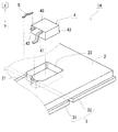
図1〜図4を参照して、実施形態1に係る回路構成体1Aを説明する。回路構成体1Aは、回路パターン21が形成される上面を有する回路基板2と、回路基板2の下面に固定されるバスバ3と、バスバ3上に配置されるパッケージ40を有する電子部品4とを備える。電子部品4は、パッケージ40から露出する第1端子41と第2端子42とを有する。第1端子41はバスバ3(31)に電気的に接続され、第2端子42は回路パターン21に電気的に接続される。回路構成体1Aの特徴の一つは、バスバ3に接することなく回路パターン21と第2端子42とを電気的に接続するフレキシブルシート部材5を備える点にある。以下、詳細を説明する。以下の説明では、説明の便宜上、回路構成体1Aの回路基板2におけるバスバ3側を下、その反対側を上として説明する。
Embodiment 1
[Circuit structure]
With reference to FIGS. 1-4, the
[回路基板]
回路基板2は、電子部品4が実装される板状部材で、電子部品4の端子(第1端子41)と電気的に接続される回路パターン21と、電子部品4をバスバ3に実装するための実装用貫通孔22とを備える(図1〜図4)。回路パターン21は、絶縁基板の一面(上面)に形成されている。回路パターン21は、必要に応じて絶縁基板の他面(下面)にも形成されていてもよい。回路パターン21は、銅箔で形成されている。回路基板2は、プリント基板を用いることができる。回路基板2の下面には、バスバ3が固定される。
[Circuit board]
The
実装用貫通孔22は、隣り合う2つのバスバ31,32に臨むように上下面を貫通している。実装用貫通孔22の輪郭形状は、電子部品4の外形に沿った形状が挙げられる。この実装用貫通孔22は、大きさの異なる大小の矩形孔が一連に形成されて構成されている。大矩形孔には、電子部品4のパッケージ40と第3端子43とが挿通され、小矩形孔には、電子部品4の第1端子41が挿通される(いずれも後述)。
The mounting through-
回路基板2の厚さは、厚くすることができる。詳しくは後述するが、フレキシブルシート部材5を備えることで、電子部品4の第2端子42を曲げなくてもよいため、その曲げのために回路基板2の厚さを考慮(薄く)する必要がないからである。回路基板2の厚さを厚くできることから、回路基板2には、表裏の一方の面に回路パターン21が形成された片面(1層)基板や表裏の両面に回路パターン21が形成された両面(2層)基板の他、多層基板を利用することもできる。回路基板2の厚さは、例えば1mm以上とすることができる。回路基板2の厚さは、実用上3mm以下とすることができる。
The thickness of the
[バスバ]
バスバ3は、電力回路を構成する(図1〜図4)。バスバ3は、電源や電気的負荷に接続される。バスバ3の材質は、導電性の金属が挙げられ、具体的には銅や銅合金などが挙げられる。バスバ3の数は複数であり、この複数のバスバ3(31,32)は、回路基板2の他面(下面)に互いに間隔を開けて固定されている(図2)。複数のバスバ3と回路基板2との固定には、これらの間に介在させる粘着シート(図示略)を用いることができる。粘着シートは、例えば、高耐熱性アクリル系粘着剤、エポキシ樹脂などの絶縁性接着剤が挙げられる。バスバ31,32の形状は、矩形状などが挙げられる。隣り合う2つのバスバ31,32の上面は、面一である。
[Busba]
The bus bar 3 constitutes a power circuit (FIGS. 1 to 4). The bus bar 3 is connected to a power source and an electrical load. Examples of the material of the bus bar 3 include conductive metals, and specifically copper and copper alloys. There are a plurality of bus bars 3, and the plurality of bus bars 3 (31, 32) are fixed to the other surface (lower surface) of the
[電子部品]
電子部品4は、回路基板2の上面の回路パターン21とバスバ3との両方に実装される(図1〜図4)。電子部品4は、バスバ3上に配置されるパッケージ40と、回路パターン21とバスバ3のそれぞれに電気的に接続される複数の端子を有する。複数の端子の配置箇所は適宜選択でき、パッケージ40の上下面・側面のいずれでもよく、各端子の配置箇所が同一面でなくてもよい。例えば、第1端子41及び第2端子42は、パッケージ40の下面以外の面に設けることが挙げられ、第3端子43は、パッケージ40の下面に設けることが挙げられる。
[Electronic parts]
The
ここでは、電子部品4は、パッケージ40の側面に設けられる第1端子41、及び第2端子42と、パッケージ40の下面に配置される第3端子43の3種類の端子を有する(図2)。パッケージ40は、両バスバ31,32間の間隔を跨がず、他方のバスバ32の上面に配置されている(図1,図3,図4)。
Here, the
第1端子41は、パッケージ40の側面から下方側(一方のバスバ31側)に延びている(図4)。図4では、説明の便宜上、紙面奥側の第2端子42などを省略して示している。この第1端子41は、両バスバ31,32間の間隔を跨いでいる。第1端子41の先端は、一方のバスバ31に電気的かつ機械的に接続されている。第1端子41の根元の上下方向の配置位置は、パッケージ40の側面において、回路基板2の上面より少し上方に位置している。
The
第2端子42は、パッケージ40における第1端子41が設けられる側面と同一側面から回路基板2に向かって直線状に張り出すように形成されている(図1,図3)。第2端子42は、後述のフレキシブルシート部材5と電気的かつ機械的に接続されていて、この接続により回路パターン21に電気的に接続されている。第2端子42の上下方向の配置位置、即ち、第2端子42におけるフレキシブルシート部材5との接続箇所は、パッケージ40の側面において、回路基板2の上面より上側でも下側でもよい、回路基板2の上面と面一でもよい。ここでは、第2端子42の上記配置位置(上記接続箇所)は、回路基板2の上面より少し上方に位置している。この第2端子42と第1端子41の根元とは同一平面上に位置している。
The
第3端子43は、パッケージ40の裏面の絶縁材を挟んで第1端子41及び第2端子42の反対側でパッケージ40に一体に設けられている(図2)。第3端子43は、第1端子41とは異なる他方のバスバ32に電気的かつ機械的に接続されている。
The
第1端子41及び第3端子43と各バスバ31,32との電気的かつ機械的な接続には、導電性接続部材、代表的にはハンダ7(図4)を用いることができる。図4では、第3端子とバスバ32との接続箇所を省略している。このハンダ7による接続は、詳しくは後述するが、リフロー方式で行うことができる。第2端子42とフレキシブルシート部材5との電気的かつ機械的な接続は、代表的にはハンダ7(図1,図3)を用いることができる。このハンダ7による接続は、ハンダ付けにより行える。なお、第2端子42とフレキシブルシート部材5との電気的かつ機械的な接続は、圧着することでも行える。即ち、第2端子42は、フレキシブルシート部材5と共に、互いに機械的に接続される圧着接続構造を構成する。
For the electrical and mechanical connection between the
第1端子41〜第3端子43の数は、電子部品4の種類などに応じて、単数としたり複数としたりすることが挙げられる。電子部品4の種類は、例えば、リレーやFET(Field effect transistor)といったスイッチング素子が挙げられる。ここでは、電子部品4は、FETを用いている。図1に示すFETの第1端子41はゲート端子で構成し、第2端子42はソース端子で構成し、第3端子43はドレイン端子で構成している。
The number of the
[フレキシブルシート部材]
フレキシブルシート部材5は、バスバ3に接することなく回路パターン21と第2端子42とを電気的に接続する。このフレキシブルシート部材5により、第2端子42を回路パターン21に直接接続しなくてもよくなるので、回路基板2の厚さ分を考慮して第2端子42を曲げる必要がなく、曲げ加工などの作業が不要にできる。バスバ3に接するとは、接着層や絶縁層などを介して接することや固定されることも含む。
[Flexible sheet material]
The
フレキシブルシート部材5の一端は、回路パターン21に電気的かつ機械的に接続され、フレキシブルシート部材5の他端は、第2端子42に電気的かつ機械的に接続されている。ここでは、フレキシブルシート部材5における第2端子42から回路パターン21までの導通経路は、両バスバ31,32の間隔を跨いでいるが、跨がない接続も可能である。この電気的かつ機械的な接続には、ハンダ7を用いることができる。なお、フレキシブルシート部材5の他端と第2端子42との電気的かつ機械的な接続は、上述したように圧着することで行ってもよい。即ち、フレキシブルシート部材5は、第2端子42と共に、互いに機械的に接続される圧着接続構造を構成する。
One end of the
フレキシブルシート部材5は、その一端(回路パターン21)と他端(第2端子42)との間に上方に突出する湾曲部51を有することが好ましい。そうすれば、振動などによる外部応力を吸収し易い。それにより、回路基板2及び第2端子42とフレキシブルシート部材5との接続状態を維持し易い。この湾曲部51の頂点は、パッケージ40の上面よりも下側に位置していることが好ましい(図3)。そうすれば、フレキシブルシート部材5が電子部品4よりも上方に位置していないため、フレキシブルシート部材5自体が邪魔にならない。図3では、説明の便宜上、パッケージ40の上面の延長面を二点鎖線で示している。頂点がパッケージ40の上面より下側に位置とは、フレキシブルシート部材5の全てがパッケージ40の上面より下側に位置していることをいう。
The
フレキシブルシート部材5の形状は、矩形状である。フレキシブルシート部材5の幅は、回路パターン21側はランドより少し小さい長さとすることが挙げられる。ここでいう幅とは、第1端子41と第2端子42の並列方向(図3の紙面直交方向)を言う。フレキシブルシート部材5の長さは、第2端子42と回路パターン21との間よりも少し長くしている。それにより、湾曲部51を形成できる。フレキシブルシート部材5の長さが長いため、フレキシブルシート部材5を回路パターン21及び第2端子42に接続する際、回路パターン21と第2端子42との間の寸法公差を吸収できて生産性に優れる。フレキシブルシート部材5の厚さは、10μm以上が好ましい。そうすれば、第2端子42及び回路パターン21に対する電気接続を確保し易い。フレキシブルシート部材5の厚さは、70μm以下が好ましい。そうすれば、可撓性(柔軟性)に優れる。フレキシブルシート部材5の厚さは、更に12μm以上35μm以下が好ましい。
The shape of the
フレキシブルシート部材5は、銅箔、FPC(Flexible Printed Circuits)などを用いることができる。
For the
[その他]
(放熱部材)
回路構成体1Aは、使用時のバスバ3の熱を放熱する放熱部材(図示略)を備えることが好ましい。放熱部材は、バスバ3の下面に配置される。放熱部材の大きさは、バスバ3の下面全面に接触可能な大きさとすることが挙げられる。放熱部材は、上下面がフラットな平板状部材で構成していてもよいし、上面がフラットな平板状部材とその平板状部材の下面から下方に突出する複数の突起で構成されるフィンとが一体に形成されていてもよい。フィンを備えれば、放熱部材の表面積を大きくして放熱性を高くし易い。
[Others]
(Heat dissipation member)
It is preferable that 1 A of circuit structures are equipped with the heat radiating member (illustration omitted) which thermally radiates the heat | fever of the bus bar 3 at the time of use. The heat dissipating member is disposed on the lower surface of the bus bar 3. The size of the heat radiating member may be a size that allows contact with the entire lower surface of the bus bar 3. The heat dissipating member may be formed of a flat plate member whose upper and lower surfaces are flat, or a flat plate member whose upper surface is flat and a fin formed of a plurality of protrusions protruding downward from the lower surface of the flat plate member. It may be formed integrally. If the fin is provided, the surface area of the heat radiating member can be increased to increase the heat dissipation.
放熱部材の上面へのバスバ3の固定は、放熱部材とバスバ3との間に接着層(図示略)を介在させることで行ってもよいし、回路基板2とバスバ3との積層体を貫通するねじ(図示略)でねじ止めすることで行ってもよいし、その両方で行ってもよい。回路基板2の厚さを厚くできるので、ねじ止めすれば放熱部材の上面へ回路基板2及びバスバ3を強固に固定し易い。ねじ止めする場合、放熱部材の上面には、ねじを螺合させるねじ穴が形成されている。放熱部材の構成材料は、熱伝導性に優れる金属材料が挙げられる。その金属材料は、例えば、アルミニウムやアルミニウム合金などが挙げられる。
The bus bar 3 may be fixed to the upper surface of the heat dissipating member by interposing an adhesive layer (not shown) between the heat dissipating member and the bus bar 3 or through the laminate of the
[用途]
回路構成体1Aは、自動車用電気接続箱に好適に利用可能である。また、回路構成体1Aは、直流電圧変換装置、AC/DC変換装置、DC/ACインバータなどの大電流パワー回路用基板に好適に利用可能である。
[Usage]
The
〔作用効果〕
実施形態1の回路構成体1Aによれば、以下の効果を奏することができる。
[Function and effect]
According to the
(1)フレキシブルシート部材5により、パッケージ40の側面から直線状に張り出した第2端子42と回路パターン21とを接続できるため、第2端子42と回路パターン21とを直接接続しなくてもよい。それにより、回路基板2の厚さ分を考慮して第2端子42を曲げる必要がなく、曲げ加工などの作業が不要にできる。そのため、電子部品4の回路基板2への実装が容易である。従って、生産性に優れる。また、第2端子42を回路パターン21と直接接続しなくてもよいので、第2端子42の長さが短く(例えば、両バスバ31,32間の間隔を跨がない程度)てもよい。そのため、リード材料を低減できる。
(1) Because the
(2)フレキシブルシート部材5を備えることで、電子部品4の第2端子42を曲げなくてもよいため、その曲げのために回路基板2の厚さを薄くする必要がない。それにより、回路基板2を厚くできる。そのため、回路基板2に多層基板を利用することもできる。また、回路基板2の厚さを厚くできるので、放熱部材の上面へ回路基板2及びバスバ3をねじ止めすることができて、回路構成体1Aを放熱部材などの設置対象に強固に固定し易い。
(2) Since the
〔回路構成体の製造方法〕
回路構成体1Aの製造は、例えば、準備工程と組合体作製工程と接続工程とを備える製造方法I、又は、準備工程と積層体作製工程とシート取付工程と塗布工程と載置工程と熱処理工程とを備える製造方法IIにより行える。以下、製造方法I、製造方法IIを順に説明する。製造方法Iと製造方法IIの違いは、電子部品4とフレキシブルシート部材5とを回路基板2とバスバ3との積層体に対して個々に接続するか、同時に接続するかにある。
[Manufacturing method of circuit structure]
The manufacture of the
[製造方法I]
(準備工程)
準備工程は、上述の回路基板2、バスバ3、電子部品4、及びフレキシブルシート部材5を準備する。
[Production Method I]
(Preparation process)
In the preparation step, the above-described
(組合体作製工程)
組合体作成工程は、回路基板2とバスバ3と電子部品4とが組み合わされた組合体を作製する。
(Union production process)
In the combination creation process, a combination is formed by combining the
まず、回路基板2とバスバ3との積層体を作製する。積層体の作製は、回路基板2の下面とバスバ3の上面とを固定することで行える。この固定は、上述したように粘着シートが利用できる。
First, a laminated body of the
次に、バスバ3の上面に電子部品4の第1端子41を接続する。電子部品4を各バスバ31,32に載置する前に、予め所定の位置に導電性接続部材、ここではハンダペーストを塗布する。具体的な塗布箇所は、両バスバ31,32における回路基板2の実装用貫通孔22から露出している箇所である。電子部品4を塗布したハンダペーストに載せてから加熱して、電子部品4の第1端子41を一方のバスバ31に接続し、第3端子43を他方のバスバ32に接続する。こうしてバスバ3と電子部品4との接続をハンダ7のリフローで行うことで、バスバ3と電子部品4との接続作業性に優れる。
Next, the
(接続工程)
接続工程は、フレキシブルシート部材5の一端、及び他端のそれぞれを、組合体における回路基板2の回路パターン21、及び電子部品4の第2端子42に接続する。この接続は、ハンダ付けにより行える。
(Connection process)
In the connection step, one end and the other end of the
[製造方法II]
(準備工程)
準備工程は、上述の製造方法Iの準備工程と同じである。
[Production Method II]
(Preparation process)
The preparation process is the same as the preparation process of manufacturing method I described above.
(積層体作製工程)
積層体作製工程は、回路基板2とバスバ3との積層体を作製する。積層体の作製は、上述のように、粘着シートを用いて回路基板2の下面とバスバ3の上面とを固定することで行える。
(Laminate production process)
In the laminated body production step, a laminated body of the
(シート取付工程)
シート取付工程は、電子部品4の第2端子42とフレキシブルシート部材5の一端とを接続してシート付き電子部品を作製する。この接続は、ハンダ付けにより行ってもよいし、両者を圧着することで行ってもよい。この接続により、フレキシブルシート部材5は、電子部品4に片持ち支持されたような状態となる。
(Sheet mounting process)
In the sheet attaching step, the
(塗布工程)
塗布工程は、上記積層体におけるバスバ3及び回路パターン21の所定の箇所に導電性接続部材を塗布する。ここでは、上述と同様、導電性接続部材にハンダペーストを利用する。ハンダペーストは、バスバ31における回路基板2の実装用貫通孔22から露出する箇所と回路パターン21とに塗布する。
(Coating process)
In the applying step, a conductive connection member is applied to predetermined portions of the bus bar 3 and the
(載置工程)
載置工程は、積層体上にシート付き電子部品を積層する。このとき、シート付き電子部品における第1端子41、及びフレキシブルシート部材5の他端と、バスバ3上の導電性接続部材、及び回路パターン21上の導電性接続部材とをそれぞれ接触させる。
(Installation process)
In the placing step, the electronic component with a sheet is laminated on the laminated body. At this time, the
(熱処理工程)
熱処理工程は、導電性接続部材に熱処理を施す。そうして、第1端子41とバスバ31とを固定し、フレキシブルシート部材5の他端と回路パターン21とを接続する。
(Heat treatment process)
In the heat treatment step, heat treatment is performed on the conductive connecting member. Then, the
〔作用効果〕
実施形態1の回路構成体の製造方法I,IIによれば、フレキシブルシート部材5を準備することで電子部品4を回路基板2へ容易に実装できる。特に、上記製造方法Iによれば、電子部品4をバスバ3に実装した後にフレキシブルシート部材5で第2端子42と回路パターン21とを接続するため、各部材を厳密に位置合わせしなくてもよいので、生産性を高め易い。特に、上記製造方法IIによれば、予め電子部品4とフレキシブルシート部材5とを一体化させたシート付き電子部品を作製しておくことで、回路基板2及びバスバ3に電子部品4とフレキシブルシート部材5とを同時に接続できるため、回路構成体1Aの生産性に優れる。
[Function and effect]
According to the manufacturing method I and II of the circuit configuration body of the first embodiment, the
本発明はこれらの例示に限定されるものではなく、特許請求の範囲によって示され、特許請求の範囲と均等の意味および範囲内でのすべての変更が含まれることが意図される。 The present invention is not limited to these exemplifications, but is defined by the scope of the claims, and is intended to include all modifications within the scope and meaning equivalent to the scope of the claims.
1A 回路構成体
2 回路基板
21 回路パターン 22 実装用貫通孔
3 バスバ
31 一方のバスバ 32 他方のバスバ
4 電子部品
40 パッケージ 41 第1端子 42 第2端子 43 第3端子
5 フレキシブルシート部材
51 湾曲部
7 ハンダ
DESCRIPTION OF
Claims (5)
前記回路基板の下面に固定されるバスバと、
前記バスバ上に配置されるパッケージと、前記パッケージから露出して前記バスバに電気的に接続される第1端子と、前記パッケージから露出して前記回路パターンに電気的に接続される第2端子とを有する電子部品と、
前記バスバに接することなく前記回路パターンと前記第2端子とを電気的に接続するフレキシブルシート部材とを備える回路構成体。 A circuit board having an upper surface on which a circuit pattern is formed;
A bus bar fixed to the lower surface of the circuit board;
A package disposed on the bus bar; a first terminal exposed from the package and electrically connected to the bus bar; and a second terminal exposed from the package and electrically connected to the circuit pattern; An electronic component having
A circuit structure comprising a flexible sheet member that electrically connects the circuit pattern and the second terminal without contacting the bus bar.
Priority Applications (2)
| Application Number | Priority Date | Filing Date | Title |
|---|---|---|---|
| JP2016101729A JP2017208508A (en) | 2016-05-20 | 2016-05-20 | Circuit structure |
| PCT/JP2017/017840 WO2017199837A1 (en) | 2016-05-20 | 2017-05-11 | Circuit structure |
Applications Claiming Priority (1)
| Application Number | Priority Date | Filing Date | Title |
|---|---|---|---|
| JP2016101729A JP2017208508A (en) | 2016-05-20 | 2016-05-20 | Circuit structure |
Publications (1)
| Publication Number | Publication Date |
|---|---|
| JP2017208508A true JP2017208508A (en) | 2017-11-24 |
Family
ID=60325172
Family Applications (1)
| Application Number | Title | Priority Date | Filing Date |
|---|---|---|---|
| JP2016101729A Pending JP2017208508A (en) | 2016-05-20 | 2016-05-20 | Circuit structure |
Country Status (2)
| Country | Link |
|---|---|
| JP (1) | JP2017208508A (en) |
| WO (1) | WO2017199837A1 (en) |
Cited By (3)
| Publication number | Priority date | Publication date | Assignee | Title |
|---|---|---|---|---|
| WO2020017468A1 (en) * | 2018-07-18 | 2020-01-23 | 株式会社オートネットワーク技術研究所 | Circuit board |
| WO2020255666A1 (en) * | 2019-06-17 | 2020-12-24 | 株式会社オートネットワーク技術研究所 | Board structure |
| CN112352473A (en) * | 2018-07-18 | 2021-02-09 | 株式会社自动网络技术研究所 | Circuit board |
Families Citing this family (1)
| Publication number | Priority date | Publication date | Assignee | Title |
|---|---|---|---|---|
| KR102609140B1 (en) | 2019-03-06 | 2023-12-05 | 삼성전기주식회사 | Coil component |
Family Cites Families (4)
| Publication number | Priority date | Publication date | Assignee | Title |
|---|---|---|---|---|
| JP2000183099A (en) * | 1998-12-16 | 2000-06-30 | Nippon Telegr & Teleph Corp <Ntt> | Ribbon for bonding |
| JP2001327044A (en) * | 2000-05-16 | 2001-11-22 | Auto Network Gijutsu Kenkyusho:Kk | Power distributor for vehicle |
| JP3809051B2 (en) * | 2000-08-01 | 2006-08-16 | 松下電工株式会社 | Electronic component mounting structure |
| JP2010178490A (en) * | 2009-01-29 | 2010-08-12 | Autonetworks Technologies Ltd | Circuit structure, and electrical connection box |
-
2016
- 2016-05-20 JP JP2016101729A patent/JP2017208508A/en active Pending
-
2017
- 2017-05-11 WO PCT/JP2017/017840 patent/WO2017199837A1/en active Application Filing
Cited By (9)
| Publication number | Priority date | Publication date | Assignee | Title |
|---|---|---|---|---|
| WO2020017468A1 (en) * | 2018-07-18 | 2020-01-23 | 株式会社オートネットワーク技術研究所 | Circuit board |
| JP2020013896A (en) * | 2018-07-18 | 2020-01-23 | 株式会社オートネットワーク技術研究所 | Circuit board |
| CN112352473A (en) * | 2018-07-18 | 2021-02-09 | 株式会社自动网络技术研究所 | Circuit board |
| CN112514542A (en) * | 2018-07-18 | 2021-03-16 | 株式会社自动网络技术研究所 | Circuit board |
| WO2020255666A1 (en) * | 2019-06-17 | 2020-12-24 | 株式会社オートネットワーク技術研究所 | Board structure |
| JP2020205335A (en) * | 2019-06-17 | 2020-12-24 | 株式会社オートネットワーク技術研究所 | Substrate structure |
| CN113906832A (en) * | 2019-06-17 | 2022-01-07 | 株式会社自动网络技术研究所 | Substrate structure |
| JP7218677B2 (en) | 2019-06-17 | 2023-02-07 | 株式会社オートネットワーク技術研究所 | Substrate structure |
| US11711887B2 (en) | 2019-06-17 | 2023-07-25 | Autonetworks Technologies, Ltd. | Substrate structure |
Also Published As
| Publication number | Publication date |
|---|---|
| WO2017199837A1 (en) | 2017-11-23 |
Similar Documents
| Publication | Publication Date | Title |
|---|---|---|
| WO2016114098A1 (en) | Circuit assembly, electrical junction box, and manufacturing method for circuit assembly | |
| CN108370142B (en) | Circuit structure and electrical junction box | |
| WO2017199837A1 (en) | Circuit structure | |
| US7919854B2 (en) | Semiconductor module with two cooling surfaces and method | |
| JP6187380B2 (en) | Circuit assembly and electrical junction box | |
| WO2015178232A1 (en) | Circuit structure and electric junction box | |
| JP6115464B2 (en) | Circuit structure | |
| JP2010129795A (en) | Semiconductor module for power | |
| WO2018207621A1 (en) | Circuit configuration and electrical connection box | |
| JP2018182147A (en) | Substrate with metal member, circuit configuration body, and electric connection box | |
| CN109995246B (en) | Switching power supply device | |
| WO2017199836A1 (en) | Circuit structure | |
| WO2018193828A1 (en) | Metal member-equipped substrate, circuit structure, and electrical connection box | |
| JP6593597B2 (en) | Circuit structure | |
| CN109698172A (en) | The manufacturing method of circuit structure and circuit structure | |
| WO2022004332A1 (en) | Circuit structure | |
| JP6667105B2 (en) | Circuit board, circuit structure, and method of manufacturing circuit board | |
| JP5445368B2 (en) | Semiconductor module and method for manufacturing semiconductor module | |
| JP2013025974A (en) | Current auxiliary member | |
| JP6065806B2 (en) | Circuit structure and method for manufacturing circuit structure | |
| WO2020246224A1 (en) | Circuit structure and electrical connection box | |
| JP2015002323A (en) | Electronic device | |
| WO2020246223A1 (en) | Circuit structure and electrical connection box | |
| WO2023282139A1 (en) | Board module, and electrical connection box | |
| WO2011115037A1 (en) | Printed circuit board and method for producing same |