JP2019087592A - Capacitor module, resonator, wireless power transmission device, wireless power reception device, and wireless power transmission system - Google Patents
Capacitor module, resonator, wireless power transmission device, wireless power reception device, and wireless power transmission system Download PDFInfo
- Publication number
- JP2019087592A JP2019087592A JP2017213477A JP2017213477A JP2019087592A JP 2019087592 A JP2019087592 A JP 2019087592A JP 2017213477 A JP2017213477 A JP 2017213477A JP 2017213477 A JP2017213477 A JP 2017213477A JP 2019087592 A JP2019087592 A JP 2019087592A
- Authority
- JP
- Japan
- Prior art keywords
- capacitor
- power transmission
- pad electrode
- wireless power
- substrate
- Prior art date
- Legal status (The legal status is an assumption and is not a legal conclusion. Google has not performed a legal analysis and makes no representation as to the accuracy of the status listed.)
- Pending
Links
Images


Classifications
-
- B—PERFORMING OPERATIONS; TRANSPORTING
- B60—VEHICLES IN GENERAL
- B60L—PROPULSION OF ELECTRICALLY-PROPELLED VEHICLES; SUPPLYING ELECTRIC POWER FOR AUXILIARY EQUIPMENT OF ELECTRICALLY-PROPELLED VEHICLES; ELECTRODYNAMIC BRAKE SYSTEMS FOR VEHICLES IN GENERAL; MAGNETIC SUSPENSION OR LEVITATION FOR VEHICLES; MONITORING OPERATING VARIABLES OF ELECTRICALLY-PROPELLED VEHICLES; ELECTRIC SAFETY DEVICES FOR ELECTRICALLY-PROPELLED VEHICLES
- B60L53/00—Methods of charging batteries, specially adapted for electric vehicles; Charging stations or on-board charging equipment therefor; Exchange of energy storage elements in electric vehicles
- B60L53/10—Methods of charging batteries, specially adapted for electric vehicles; Charging stations or on-board charging equipment therefor; Exchange of energy storage elements in electric vehicles characterised by the energy transfer between the charging station and the vehicle
- B60L53/12—Inductive energy transfer
-
- H—ELECTRICITY
- H01—ELECTRIC ELEMENTS
- H01G—CAPACITORS; CAPACITORS, RECTIFIERS, DETECTORS, SWITCHING DEVICES OR LIGHT-SENSITIVE DEVICES, OF THE ELECTROLYTIC TYPE
- H01G4/00—Fixed capacitors; Processes of their manufacture
- H01G4/38—Multiple capacitors, i.e. structural combinations of fixed capacitors
-
- H—ELECTRICITY
- H02—GENERATION; CONVERSION OR DISTRIBUTION OF ELECTRIC POWER
- H02J—CIRCUIT ARRANGEMENTS OR SYSTEMS FOR SUPPLYING OR DISTRIBUTING ELECTRIC POWER; SYSTEMS FOR STORING ELECTRIC ENERGY
- H02J50/00—Circuit arrangements or systems for wireless supply or distribution of electric power
- H02J50/005—Mechanical details of housing or structure aiming to accommodate the power transfer means, e.g. mechanical integration of coils, antennas or transducers into emitting or receiving devices
-
- H—ELECTRICITY
- H03—ELECTRONIC CIRCUITRY
- H03H—IMPEDANCE NETWORKS, e.g. RESONANT CIRCUITS; RESONATORS
- H03H7/00—Multiple-port networks comprising only passive electrical elements as network components
- H03H7/01—Frequency selective two-port networks
- H03H7/0115—Frequency selective two-port networks comprising only inductors and capacitors
-
- H—ELECTRICITY
- H05—ELECTRIC TECHNIQUES NOT OTHERWISE PROVIDED FOR
- H05K—PRINTED CIRCUITS; CASINGS OR CONSTRUCTIONAL DETAILS OF ELECTRIC APPARATUS; MANUFACTURE OF ASSEMBLAGES OF ELECTRICAL COMPONENTS
- H05K1/00—Printed circuits
- H05K1/02—Details
- H05K1/0271—Arrangements for reducing stress or warp in rigid printed circuit boards, e.g. caused by loads, vibrations or differences in thermal expansion
-
- H—ELECTRICITY
- H05—ELECTRIC TECHNIQUES NOT OTHERWISE PROVIDED FOR
- H05K—PRINTED CIRCUITS; CASINGS OR CONSTRUCTIONAL DETAILS OF ELECTRIC APPARATUS; MANUFACTURE OF ASSEMBLAGES OF ELECTRICAL COMPONENTS
- H05K1/00—Printed circuits
- H05K1/02—Details
- H05K1/11—Printed elements for providing electric connections to or between printed circuits
- H05K1/111—Pads for surface mounting, e.g. lay-out
- H05K1/112—Pads for surface mounting, e.g. lay-out directly combined with via connections
-
- H—ELECTRICITY
- H05—ELECTRIC TECHNIQUES NOT OTHERWISE PROVIDED FOR
- H05K—PRINTED CIRCUITS; CASINGS OR CONSTRUCTIONAL DETAILS OF ELECTRIC APPARATUS; MANUFACTURE OF ASSEMBLAGES OF ELECTRICAL COMPONENTS
- H05K1/00—Printed circuits
- H05K1/18—Printed circuits structurally associated with non-printed electric components
- H05K1/181—Printed circuits structurally associated with non-printed electric components associated with surface mounted components
-
- H—ELECTRICITY
- H05—ELECTRIC TECHNIQUES NOT OTHERWISE PROVIDED FOR
- H05K—PRINTED CIRCUITS; CASINGS OR CONSTRUCTIONAL DETAILS OF ELECTRIC APPARATUS; MANUFACTURE OF ASSEMBLAGES OF ELECTRICAL COMPONENTS
- H05K3/00—Apparatus or processes for manufacturing printed circuits
- H05K3/30—Assembling printed circuits with electric components, e.g. with resistor
- H05K3/32—Assembling printed circuits with electric components, e.g. with resistor electrically connecting electric components or wires to printed circuits
- H05K3/34—Assembling printed circuits with electric components, e.g. with resistor electrically connecting electric components or wires to printed circuits by soldering
- H05K3/341—Surface mounted components
- H05K3/3431—Leadless components
- H05K3/3442—Leadless components having edge contacts, e.g. leadless chip capacitors, chip carriers
-
- B—PERFORMING OPERATIONS; TRANSPORTING
- B60—VEHICLES IN GENERAL
- B60L—PROPULSION OF ELECTRICALLY-PROPELLED VEHICLES; SUPPLYING ELECTRIC POWER FOR AUXILIARY EQUIPMENT OF ELECTRICALLY-PROPELLED VEHICLES; ELECTRODYNAMIC BRAKE SYSTEMS FOR VEHICLES IN GENERAL; MAGNETIC SUSPENSION OR LEVITATION FOR VEHICLES; MONITORING OPERATING VARIABLES OF ELECTRICALLY-PROPELLED VEHICLES; ELECTRIC SAFETY DEVICES FOR ELECTRICALLY-PROPELLED VEHICLES
- B60L53/00—Methods of charging batteries, specially adapted for electric vehicles; Charging stations or on-board charging equipment therefor; Exchange of energy storage elements in electric vehicles
- B60L53/30—Constructional details of charging stations
- B60L53/34—Plug-like or socket-like devices specially adapted for contactless inductive charging of electric vehicles
-
- B—PERFORMING OPERATIONS; TRANSPORTING
- B60—VEHICLES IN GENERAL
- B60Y—INDEXING SCHEME RELATING TO ASPECTS CROSS-CUTTING VEHICLE TECHNOLOGY
- B60Y2200/00—Type of vehicle
- B60Y2200/90—Vehicles comprising electric prime movers
- B60Y2200/91—Electric vehicles
-
- H—ELECTRICITY
- H01—ELECTRIC ELEMENTS
- H01G—CAPACITORS; CAPACITORS, RECTIFIERS, DETECTORS, SWITCHING DEVICES OR LIGHT-SENSITIVE DEVICES, OF THE ELECTROLYTIC TYPE
- H01G2/00—Details of capacitors not covered by a single one of groups H01G4/00-H01G11/00
- H01G2/02—Mountings
- H01G2/06—Mountings specially adapted for mounting on a printed-circuit support
-
- H—ELECTRICITY
- H01—ELECTRIC ELEMENTS
- H01G—CAPACITORS; CAPACITORS, RECTIFIERS, DETECTORS, SWITCHING DEVICES OR LIGHT-SENSITIVE DEVICES, OF THE ELECTROLYTIC TYPE
- H01G4/00—Fixed capacitors; Processes of their manufacture
- H01G4/40—Structural combinations of fixed capacitors with other electric elements, the structure mainly consisting of a capacitor, e.g. RC combinations
-
- H—ELECTRICITY
- H02—GENERATION; CONVERSION OR DISTRIBUTION OF ELECTRIC POWER
- H02J—CIRCUIT ARRANGEMENTS OR SYSTEMS FOR SUPPLYING OR DISTRIBUTING ELECTRIC POWER; SYSTEMS FOR STORING ELECTRIC ENERGY
- H02J2310/00—The network for supplying or distributing electric power characterised by its spatial reach or by the load
- H02J2310/40—The network being an on-board power network, i.e. within a vehicle
- H02J2310/48—The network being an on-board power network, i.e. within a vehicle for electric vehicles [EV] or hybrid vehicles [HEV]
-
- H—ELECTRICITY
- H02—GENERATION; CONVERSION OR DISTRIBUTION OF ELECTRIC POWER
- H02J—CIRCUIT ARRANGEMENTS OR SYSTEMS FOR SUPPLYING OR DISTRIBUTING ELECTRIC POWER; SYSTEMS FOR STORING ELECTRIC ENERGY
- H02J50/00—Circuit arrangements or systems for wireless supply or distribution of electric power
- H02J50/10—Circuit arrangements or systems for wireless supply or distribution of electric power using inductive coupling
- H02J50/12—Circuit arrangements or systems for wireless supply or distribution of electric power using inductive coupling of the resonant type
-
- H—ELECTRICITY
- H05—ELECTRIC TECHNIQUES NOT OTHERWISE PROVIDED FOR
- H05K—PRINTED CIRCUITS; CASINGS OR CONSTRUCTIONAL DETAILS OF ELECTRIC APPARATUS; MANUFACTURE OF ASSEMBLAGES OF ELECTRICAL COMPONENTS
- H05K2201/00—Indexing scheme relating to printed circuits covered by H05K1/00
- H05K2201/09—Shape and layout
- H05K2201/09009—Substrate related
- H05K2201/09063—Holes or slots in insulating substrate not used for electrical connections
-
- H—ELECTRICITY
- H05—ELECTRIC TECHNIQUES NOT OTHERWISE PROVIDED FOR
- H05K—PRINTED CIRCUITS; CASINGS OR CONSTRUCTIONAL DETAILS OF ELECTRIC APPARATUS; MANUFACTURE OF ASSEMBLAGES OF ELECTRICAL COMPONENTS
- H05K2201/00—Indexing scheme relating to printed circuits covered by H05K1/00
- H05K2201/09—Shape and layout
- H05K2201/09009—Substrate related
- H05K2201/09072—Hole or recess under component or special relationship between hole and component
-
- H—ELECTRICITY
- H05—ELECTRIC TECHNIQUES NOT OTHERWISE PROVIDED FOR
- H05K—PRINTED CIRCUITS; CASINGS OR CONSTRUCTIONAL DETAILS OF ELECTRIC APPARATUS; MANUFACTURE OF ASSEMBLAGES OF ELECTRICAL COMPONENTS
- H05K2201/00—Indexing scheme relating to printed circuits covered by H05K1/00
- H05K2201/10—Details of components or other objects attached to or integrated in a printed circuit board
- H05K2201/10007—Types of components
- H05K2201/10015—Non-printed capacitor
-
- H—ELECTRICITY
- H05—ELECTRIC TECHNIQUES NOT OTHERWISE PROVIDED FOR
- H05K—PRINTED CIRCUITS; CASINGS OR CONSTRUCTIONAL DETAILS OF ELECTRIC APPARATUS; MANUFACTURE OF ASSEMBLAGES OF ELECTRICAL COMPONENTS
- H05K2201/00—Indexing scheme relating to printed circuits covered by H05K1/00
- H05K2201/10—Details of components or other objects attached to or integrated in a printed circuit board
- H05K2201/10431—Details of mounted components
- H05K2201/10507—Involving several components
- H05K2201/10522—Adjacent components
-
- H—ELECTRICITY
- H05—ELECTRIC TECHNIQUES NOT OTHERWISE PROVIDED FOR
- H05K—PRINTED CIRCUITS; CASINGS OR CONSTRUCTIONAL DETAILS OF ELECTRIC APPARATUS; MANUFACTURE OF ASSEMBLAGES OF ELECTRICAL COMPONENTS
- H05K2201/00—Indexing scheme relating to printed circuits covered by H05K1/00
- H05K2201/10—Details of components or other objects attached to or integrated in a printed circuit board
- H05K2201/10431—Details of mounted components
- H05K2201/10507—Involving several components
- H05K2201/10545—Related components mounted on both sides of the PCB
-
- Y—GENERAL TAGGING OF NEW TECHNOLOGICAL DEVELOPMENTS; GENERAL TAGGING OF CROSS-SECTIONAL TECHNOLOGIES SPANNING OVER SEVERAL SECTIONS OF THE IPC; TECHNICAL SUBJECTS COVERED BY FORMER USPC CROSS-REFERENCE ART COLLECTIONS [XRACs] AND DIGESTS
- Y02—TECHNOLOGIES OR APPLICATIONS FOR MITIGATION OR ADAPTATION AGAINST CLIMATE CHANGE
- Y02P—CLIMATE CHANGE MITIGATION TECHNOLOGIES IN THE PRODUCTION OR PROCESSING OF GOODS
- Y02P70/00—Climate change mitigation technologies in the production process for final industrial or consumer products
- Y02P70/50—Manufacturing or production processes characterised by the final manufactured product
-
- Y—GENERAL TAGGING OF NEW TECHNOLOGICAL DEVELOPMENTS; GENERAL TAGGING OF CROSS-SECTIONAL TECHNOLOGIES SPANNING OVER SEVERAL SECTIONS OF THE IPC; TECHNICAL SUBJECTS COVERED BY FORMER USPC CROSS-REFERENCE ART COLLECTIONS [XRACs] AND DIGESTS
- Y02—TECHNOLOGIES OR APPLICATIONS FOR MITIGATION OR ADAPTATION AGAINST CLIMATE CHANGE
- Y02T—CLIMATE CHANGE MITIGATION TECHNOLOGIES RELATED TO TRANSPORTATION
- Y02T10/00—Road transport of goods or passengers
- Y02T10/60—Other road transportation technologies with climate change mitigation effect
- Y02T10/70—Energy storage systems for electromobility, e.g. batteries
-
- Y—GENERAL TAGGING OF NEW TECHNOLOGICAL DEVELOPMENTS; GENERAL TAGGING OF CROSS-SECTIONAL TECHNOLOGIES SPANNING OVER SEVERAL SECTIONS OF THE IPC; TECHNICAL SUBJECTS COVERED BY FORMER USPC CROSS-REFERENCE ART COLLECTIONS [XRACs] AND DIGESTS
- Y02—TECHNOLOGIES OR APPLICATIONS FOR MITIGATION OR ADAPTATION AGAINST CLIMATE CHANGE
- Y02T—CLIMATE CHANGE MITIGATION TECHNOLOGIES RELATED TO TRANSPORTATION
- Y02T10/00—Road transport of goods or passengers
- Y02T10/60—Other road transportation technologies with climate change mitigation effect
- Y02T10/7072—Electromobility specific charging systems or methods for batteries, ultracapacitors, supercapacitors or double-layer capacitors
-
- Y—GENERAL TAGGING OF NEW TECHNOLOGICAL DEVELOPMENTS; GENERAL TAGGING OF CROSS-SECTIONAL TECHNOLOGIES SPANNING OVER SEVERAL SECTIONS OF THE IPC; TECHNICAL SUBJECTS COVERED BY FORMER USPC CROSS-REFERENCE ART COLLECTIONS [XRACs] AND DIGESTS
- Y02—TECHNOLOGIES OR APPLICATIONS FOR MITIGATION OR ADAPTATION AGAINST CLIMATE CHANGE
- Y02T—CLIMATE CHANGE MITIGATION TECHNOLOGIES RELATED TO TRANSPORTATION
- Y02T90/00—Enabling technologies or technologies with a potential or indirect contribution to GHG emissions mitigation
- Y02T90/10—Technologies relating to charging of electric vehicles
- Y02T90/14—Plug-in electric vehicles
Abstract
Description
本発明は、コンデンサモジュール、そのようなコンデンサモジュールを備える共振器、並びに、そのような共振器を含むワイヤレス送電装置、ワイヤレス受電装置、及びワイヤレス電力伝送システムに関する。 The present invention relates to a capacitor module, a resonator including such a capacitor module, and a wireless power transmitting apparatus, a wireless power receiving apparatus, and a wireless power transmission system including such a resonator.
近年、磁界共鳴方式を用いてワイヤレス電力伝送を行うワイヤレス電力伝送技術が注目されている。例えば、電気自動車などの電動車両に搭載されたバッテリー(二次電池)に対して充電を行う際に、このワイヤレス電力伝送技術を用いることで、充電ケーブルとの接続を行わずに、外部からの電力をワイヤレスで供給(非接触充電又は非接触給電という。)することが可能である。 In recent years, wireless power transmission technology for performing wireless power transmission using a magnetic field resonance method has attracted attention. For example, when charging a battery (secondary battery) mounted on an electrically powered vehicle such as an electric vehicle, this wireless power transmission technology is used to connect the charging cable from outside without being connected. Power can be supplied wirelessly (referred to as contactless charging or contactless power feeding).
また、ワイヤレス電力伝送技術では、2つの共振器の間における共振(共鳴)現象を利用した磁界共鳴方式の検討が活発化してきている(例えば、下記特許文献1,2を参照。)。磁界共鳴方式では、送電側及び受電側の共振器において、コイルとキャパシタ(コンデンサ)とを含む共振回路を用いる。磁界共鳴方式では、これら2つの共振器間の共振周波数を近づけて(一致させる場合も含む。)、この共振周波数付近の高周波電流及び電圧を送電(一次)側の共振器に印加し、電磁的に共振(共鳴)させた受電(二次)側の共振器に電力をワイヤレスで伝送する仕組みである。
Moreover, in the wireless power transmission technology, examination of a magnetic field resonance system using a resonance (resonance) phenomenon between two resonators has been activated (see, for example,
この磁界共鳴方式では、送電側コイルと受電側コイルとを電磁誘導の原理を用いて電磁的に結合させる電磁誘導方式に比べて、送電側コイルと受電側コイルとの間の距離を大きくできるメリットがある。また、磁界共鳴方式では、数cm〜数十cm程度の距離で数kW以上の電力をワイヤレスで伝送できることから、様々なシステムへの応用が模索されている。 In this magnetic field resonance system, the distance between the power transmission coil and the power reception coil can be increased as compared with the electromagnetic induction system in which the power transmission coil and the power reception coil are electromagnetically coupled using the principle of electromagnetic induction. There is. Further, in the magnetic field resonance method, since power of several kW or more can be wirelessly transmitted at a distance of several cm to several tens cm, application to various systems is being explored.
ところで、上述した電気自動車に対してワイヤレス電力伝送を行う場合には、送電側及び受電側の共振器に対して、大容量の高周波電流及び電圧が印加される。これに対応するため、上述した共振器を構成するキャパシタについては、プリント配線基板の主面上に複数のチップコンデンサ(コンデンサ素子)をアレイ状に並べて実装したコンデンサモジュールが用いられている(例えば、上記特許文献3を参照。)。
By the way, when performing wireless power transmission to the electric vehicle described above, a large-capacity high frequency current and voltage are applied to the resonators on the power transmission side and the power reception side. In order to cope with this, a capacitor module in which a plurality of chip capacitors (capacitor elements) are arrayed and mounted on the main surface of a printed wiring board is used as the capacitor constituting the above-mentioned resonator (for example, See
また、コンデンサモジュールでは、各チップコンデンサの両端に設けられた一対の端子電極と、プリント配線基板上に設けられた一対のパッド電極とがはんだ接合されることによって、各チップコンデンサがプリント配線基板上に実装された構造となっている。 Further, in the capacitor module, each chip capacitor is formed on the printed wiring board by soldering a pair of terminal electrodes provided on both ends of each chip capacitor and a pair of pad electrodes provided on the printed wiring board. Has a structure implemented in.
しかしながら、従来のコンデンサモジュールでは、チップコンデンサとプリント配線基板との熱膨張係数が異なることから、環境温度の変化によって、はんだ接合部にクリープ歪が発生する。さらに、その累積によってはんだクラックが生じた場合、端子電極とパッド電極との間で断線してしまうことがあった。 However, in the conventional capacitor module, since the thermal expansion coefficients of the chip capacitor and the printed wiring board are different, creep distortion occurs in the solder joint due to the change of the environmental temperature. Furthermore, when solder cracks occur due to the accumulation, disconnection may occur between the terminal electrode and the pad electrode.
特に、車両に搭載する用途においては、このはんだクラックによる断線寿命を向上させることが求められる。しかしながら、部品サイズが大きくなるに従って、熱サイクルによる疲労寿命は一般的に短くなる傾向にある。このため、車載用途には、大型の電気部品(例えば、チップタイプのコンデンサや抵抗など。)が使用できない傾向にあった。 In particular, in an application to be mounted on a vehicle, it is required to improve the disconnection life due to the solder crack. However, as the part size increases, the fatigue life due to thermal cycling generally tends to be shorter. For this reason, in on-vehicle applications, large-sized electrical components (for example, chip-type capacitors, resistors, etc.) tend not to be used.
なお、本発明に関連する先行技術文献としては、例えば上記特許文献4〜6を挙げることができる。このうち、上記特許文献4には、マイクロストリップライン間のギャップにあたる誘電体基板からグランド層に亘って、直方体状の貫通穴が設けられた構成が開示されている。 Examples of prior art documents related to the present invention include the above-mentioned Patent Documents 4 to 6. Among them, Patent Document 4 discloses a configuration in which a rectangular parallelepiped shaped through hole is provided from the dielectric substrate corresponding to the gap between the microstrip lines to the ground layer.
一方、上記特許文献5には、チップコンデンサの一対の端子間に薄板を貫通する穴状部が設けられた構成が開示されている。 On the other hand, Patent Document 5 discloses a configuration in which a hole-like portion penetrating a thin plate is provided between a pair of terminals of a chip capacitor.
一方、上記特許文献6には、基板の一面に形成された一方のランドが基板を貫通するスルーホールを介して基板の他面に形成された他方のランドと導電接続された構成が開示されている。 On the other hand, Patent Document 6 discloses a configuration in which one land formed on one surface of a substrate is conductively connected to the other land formed on the other surface of the substrate through a through hole penetrating the substrate. There is.
しかしながら、これら特許文献4〜6に記載の貫通孔は、何れもはんだクラックの発生を防ぐことについて検討されておらず、本発明とはその貫通孔を設ける目的が異なっている。 However, none of the through holes described in these Patent Documents 4 to 6 have been studied for preventing the occurrence of solder cracks, and the purpose of providing the through holes is different from the present invention.
本発明の一態様は、このような従来の事情に鑑みて提案されたものであり、コンデンサ素子側の端子電極と基板側のパッド電極とのはんだ接合された部分において、はんだクラックが発生することを抑制したコンデンサモジュール、そのようなコンデンサモジュールを備える共振器、並びに、そのような共振器を含むワイヤレス送電装置、ワイヤレス受電装置、及びワイヤレス電力伝送システムを提供することを目的の一つとする。 One aspect of the present invention has been proposed in view of such conventional circumstances, and a solder crack is generated in a portion where a terminal electrode on the capacitor element side and a pad electrode on the substrate side are soldered together. SUMMARY OF THE INVENTION It is an object of the present invention to provide a reduced capacitor module, a resonator including such a capacitor module, and a wireless power transmitting apparatus, a wireless power receiving apparatus, and a wireless power transmission system including such a resonator.
本発明の一態様に係るコンデンサモジュールは、厚み方向において互いに対向する第1の主面と第2の主面とを有する基板と、前記基板の少なくとも前記第1の主面上に実装されるコンデンサ素子とを備え、前記基板は、前記コンデンサ素子の一端側に設けられた第1の端子電極とはんだ接合される第1のパッド電極と、前記コンデンサ素子の他端側に設けられた第2の端子電極とはんだ接合される第2のパッド電極とを有し、少なくとも前記第1のパッド電極と前記第2のパッド電極との間の領域と、その領域の外側との境界を区画する一対の境界ラインと平面視で重なる位置に、前記基板を厚み方向に貫通する貫通孔が各々設けられていることを特徴とする。 A capacitor module according to an aspect of the present invention includes a substrate having a first main surface and a second main surface facing each other in a thickness direction, and a capacitor mounted on at least the first main surface of the substrate A first pad electrode soldered to a first terminal electrode provided on one end side of the capacitor element, and a second pad electrode provided on the other end side of the capacitor element. A pair of second pad electrodes soldered to the terminal electrode, and defining a boundary between an area between at least the first pad electrode and the second pad electrode and the outside of the area Through holes are provided at positions overlapping the boundary line in a plan view, respectively, and penetrating the substrate in the thickness direction.
以上のように、本発明の一態様によれば、コンデンサ素子側の端子電極と基板側のパッド電極とのはんだ接合された部分において、はんだクラックが発生することを抑制したコンデンサモジュールを提供することが可能である。また、そのようなコンデンサモジュールを備える共振器、並びに、そのような共振器を含むワイヤレス送電装置、ワイヤレス受電装置、及びワイヤレス電力伝送システムを提供することが可能である。 As described above, according to one aspect of the present invention, there is provided a capacitor module in which the occurrence of solder cracks is suppressed in a portion where a terminal electrode on the capacitor element side and a pad electrode on the substrate are soldered together. Is possible. In addition, it is possible to provide a resonator including such a capacitor module, and a wireless power transmission device, a wireless power reception device, and a wireless power transmission system including such a resonator.
以下、本発明の実施の形態について、図面を参照して詳細に説明する。
なお、以下の説明で用いる図面は、特徴をわかりやすくするために、便宜上特徴となる部分を拡大して示している場合があり、各構成要素の寸法比率などが実際と同じであるとは限らないものとする。また、以下の説明において例示される材料や寸法等は一例であって、本発明はそれらに必ずしも限定されるものではなく、その要旨を変更しない範囲で適宜変更して実施することが可能である。
Hereinafter, embodiments of the present invention will be described in detail with reference to the drawings.
In the drawings used in the following description, in order to make the features easy to understand, the features that are the features may be enlarged for the sake of convenience, and the dimensional ratio of each component may be limited to the same as the actual Make it not exist. Further, the materials, dimensions, etc. exemplified in the following description are merely examples, and the present invention is not necessarily limited to them, and can be appropriately changed and implemented without changing the gist of the invention. .
(ワイヤレス電力伝送システム)
先ず、本発明の一実施形態として、例えば図1及び図2に示すワイヤレス電力伝送システム100について説明する。なお、図1は、ワイヤレス電力伝送システム100の一例を示す構成図である。図2は、ワイヤレス電力伝送システム100の送電側共振器203及び受電側共振器301の構成を示す回路図である。
(Wireless power transfer system)
First, as an embodiment of the present invention, for example, a wireless
本実施形態のワイヤレス電力伝送システム100は、図1及び図2に示すように、電気自動車EVに搭載されたバッテリー(二次電池)に対して非接触充電を行う非接触充電システムに本発明を適用したものである。なお、電気自動車EVは、バッテリーに充電された電力によりモーターを駆動して走行する電動車両(移動体)である。
As shown in FIGS. 1 and 2, the wireless
具体的に、本実施形態のワイヤレス電力伝送システム100は、磁界共鳴方式を用いてワイヤレス電力伝送を行うものであり、充電設備側の地面Gに設置されたワイヤレス送電装置(以下、「送電装置」という。)200と、電気自動車EVに搭載されたワイヤレス受電装置(以下、「受電装置」という。)300と備えて構成されている。
Specifically, the wireless
送電装置200は、電源回路201と、駆動回路202と、送電側共振器203とを概略備えている。一方、受電装置300は、受電側共振器301と、負荷302とを概略備えている。また、負荷302は、整流回路303と、可変負荷Vloadとから構成されている。
The
電源回路201は、外部の商用電源Pと電気的に接続されて、商用電源Pから入力される交流電力を所望の直流電力に変換するAC/DC電源として機能する。電源回路201は、駆動回路202と電気的に接続されている。電源回路201は、変換された直流電力を駆動回路202に供給する。
The
なお、電源回路201については、駆動回路202に対して直流電力を出力するものであればよく、その構成について特に制限されるものではない。例えば、電源回路201としては、交流電力を整流して直流電力に変換する整流回路と、力率改善を行うPFC(Power Factor Correction)回路とを組み合わせた電源回路や、同じく整流回路と、スイッチングコンバータ等のスイッチング回路とを組み合わせた電源回路などが挙げられる。
The
駆動回路202は、電源回路201から供給される直流電力を高周波電力に変換するものである。駆動回路202としては、例えば複数のスイッチング素子がブリッジ接続されたスイッチング回路等が挙げられる。駆動回路202は、送電側共振器203と電気的に接続されている。駆動回路202は、送電側共振器203の共振周波数に基づいて駆動周波数が制御された高周波電力を送電側共振器203に供給する。
The
送電側共振器203は、送電側コイルL1と、送電側キャパシタC1とを含むLC共振回路を構成している。この送電側共振器203側の共振周波数を受電側共振器301側の共振周波数に近づける(一致させる場合も含む。)ことで、磁界共鳴方式のワイヤレス電力伝送が可能となっている。
The
本実施形態の送電側共振器203では、リアクトルLsが送電側キャパシタC1に対して直列に挿入された構成となっている。この構成の場合、送電側共振器203、受電側共振器301及び負荷302で構成されるワイヤレス電力伝送網のインピーダンスの虚部が正となるように制御し易くなる。また、リアクトルLsは、送電側共振器203側の共振周波数よりも十分高い周波数成分に対してハイインピーダンスとなる。これにより、高周波成分が除去された電力を送電側コイルL1に供給するフィルターとしての役割を果たすことになる。
In the
送電側コイルL1は、例えば銅やアルミニウム等からなるリッツ線をスパイラル状に巻き回したワイヤレス電力伝送用コイルにより構成されている。本実施形態の送電側コイルL1は、電気自動車EVのフロア下と向かい合うように、地面Gの上に設置又は地面Gに埋設されている。なお、本実施形態では、送電側コイルL1(送電側共振器203)が電源回路201と共に地面Gの上に設置された構成となっている。
The power transmission coil L1 is configured by a coil for wireless power transmission in which a litz wire made of, for example, copper, aluminum or the like is spirally wound. The power transmission coil L1 of the present embodiment is installed on the ground G or buried in the ground G so as to face the bottom of the floor of the electric vehicle EV. In the present embodiment, the power transmission coil L1 (power transmission resonator 203) is installed on the ground G together with the
送電側キャパシタC1は、駆動周波数及び負荷302の両端電圧を調整する機能を有している。本実施形態の送電側キャパシタC1は、送電側コイルL1に対して直列に接続された第1のキャパシタC11と、送電側コイルL1に対して並列に接続された第2のキャパシタC12とにより構成されているが、このような構成に必ずしも限定されるものではない。例えば、送電側コイルL1に直列に接続された第1のキャパシタC11のみからなる構成であってもよい。
The power transmission capacitor C1 has a function of adjusting the drive frequency and the voltage across the
受電側共振器301は、受電側コイルL2と、受電側キャパシタC2とを含むLC共振回路を構成している。この受電側共振器301側の共振周波数を送電側共振器203側の共振周波数に近づける(一致させる場合も含む。)ことで、磁界共鳴方式のワイヤレス電力伝送が可能となっている。
The power receiving
本実施形態の受電側共振器301では、リアクトルLrが受電側キャパシタC2に対して直列に挿入された構成となっている。この構成の場合、リアクトルLrは、受電側共振器301側の共振周波数よりも十分高い周波数成分に対してハイインピーダンスとなる。これにより、高周波成分が除去された電力を負荷302に供給するフィルターとしての役割を果たすことになる。
In power
受電側コイルL2は、例えば銅やアルミニウム等からなるリッツ線をスパイラル状に巻き回したワイヤレス電力伝送用コイルにより構成されている。本実施形態の受電側コイルL2は、上述した地面Gの上に設置又は地面Gに埋設された送電側コイルL1と向かい合うように、電気自動車EVのフロア下に設置されている。 The power receiving coil L2 is configured by a coil for wireless power transmission in which a litz wire made of, for example, copper, aluminum or the like is spirally wound. The power receiving coil L2 of the present embodiment is installed under the floor of the electric vehicle EV so as to face the power transmitting coil L1 installed on the ground G described above or embedded in the ground G.
受電側キャパシタC2は、駆動周波数及び負荷302の両端電圧を調整する機能を有している。本実施形態の受電側キャパシタC2は、受電側コイルL2に対して直列に接続された第3のキャパシタC21と、受電側コイルL2に対して並列に接続された第4のキャパシタC22とにより構成されているが、このような構成に必ずしも限定されるものではない。例えば、受電側コイルL2に直列に接続された第3のキャパシタC21のみからなる構成であってもよい。
The power receiving capacitor C2 has a function of adjusting the driving frequency and the voltage across the
整流回路303は、受電側共振器301と電気的に接続されて、受電側コイルL2が受電した高周波電力を整流して直流電力に変換するものである。整流回路303としては、例えば1つのスイッチング素子又はダイオードと平滑コンデンサとから構成される半波整流回路や、ブリッジ接続された4つのスイッチング素子又はダイオードと平滑コンデンサとから構成される全波整流回路等が挙げられる。整流回路303は、可変負荷Vloadと電気的に接続されている。整流回路303は、変換された直流電力を可変負荷Vloadに供給する。なお、受電装置300では、整流回路303と可変負荷Vloadとの間に充電器を備えた構成としてもよい。
The rectifying
可変負荷Vloadは、整流回路303の出力端子の間に接続されて、この整流回路303から供給される直流電力を貯蔵又は消費する。可変負荷Vloadとしては、上述した電気自動車EVに搭載されたバッテリーやモーター等が挙げられる。
The variable load Vload is connected between the output terminals of the
可変負荷Vloadは、電力の需要状態(貯蔵状態又は消費状態)によって、負荷302の等価抵抗値が時間と共に変わる抵抗負荷と見なすことができる。なお、整流回路303での消費電力は、可変負荷Vloadでの消費電力に比べて十分小さいため、負荷302の等価抵抗値は、ほぼ可変負荷Vloadの等価抵抗値とみなしてよい。
The variable load Vload can be regarded as a resistive load in which the equivalent resistance value of the
以上のような構成を有する本実施形態の電力伝送システム100では、送電側共振器203と受電側共振器301との間における共振(共鳴)現象を利用した磁界共鳴方式によって、送電装置200から受電装置300に向けて、電力をワイヤレスで伝送することが可能である。すなわち、この磁界共鳴方式では、これら2つの共振器203,301間の共振周波数を近づけて(一致させる場合も含む。)、この共振周波数付近の高周波電流及び電圧を送電側共振器203に印加し、電磁的に共振(共鳴)させた受電側共振器301に電力をワイヤレスで伝送(供給)することが可能である。
In
したがって、本実施形態の電力伝送システム100では、充電ケーブルとの接続を行わずに、充電設備側から供給される電力をワイヤレスで電気自動車EVに伝送しながら、この電気自動車EVに搭載されたバッテリーに対して非接触充電を行うことが可能である。
Therefore, in the
(コンデンサモジュール)
次に、本発明を適用したコンデンサモジュールとして、例えば図3〜図7に示すコンデンサモジュール1について説明する。
(Capacitor module)
Next, as a capacitor module to which the present invention is applied, for example, a
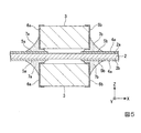
なお、図3は、コンデンサモジュール1の構成を示す平面図である。図4は、コンデンサモジュール1の要部を拡大した平面図である。図5は、図4中に示す線分A−Aによるコンデンサモジュール1の断面図である。図6は、図4中に示す線分B−Bによるコンデンサモジュール1の断面図である。図7は、コンデンサモジュール1の基板2の要部を拡大した平面図である。
FIG. 3 is a plan view showing the configuration of the
また、以下に示す図面では、XYZ直交座標系を設定し、X軸方向をコンデンサモジュール1の水平面内における第1の方向、Y軸方向をコンデンサモジュール1の水平面内における第2の方向、Z軸方向をコンデンサモジュール1の厚み方向として、それぞれ示すものとする。
Further, in the drawings shown below, an XYZ orthogonal coordinate system is set, the X-axis direction is a first direction in the horizontal surface of the
本実施形態のコンデンサモジュール1は、図3〜図7に示すように、厚み方向において互いに対向する第1の主面2aと第2の主面2bとを有する基板2と、この基板2の少なくとも第1の主面2a(本実施形態では両主面2a,2b)上にアレイ状に並んで実装された複数のコンデンサ素子3を含むコンデンサ素子群30とを備えている。
The
また、本実施形態のコンデンサモジュール1は、第1の主面2a上及び第2の主面2b上の平面視で重なる位置に、複数のコンデンサ素子3が各々実装された構造を有している。すなわち、このコンデンサモジュール1は、基板2の第1の主面2a側と第2の主面2b側とにおいて、基本的に同じ(基板2を挟んで対称となる)実装構造を有している。
In addition, the
したがって、本実施形態では、基板2の第1の主面(上面)2a側の実装構造について説明し、特に断りがない限り、基板2の第2の主面(下面)2b側の実装構造については、その説明を省略するものとする。
Therefore, in the present embodiment, the mounting structure on the first main surface (upper surface) 2a side of the
コンデンサ素子群30は、基板2の面内において互いに交差(本実施形態では直交)する第1の方向(X軸方向)と第2の方向(Y軸方向)とのうち、第1の方向に並ぶ複数のコンデンサ素子3が互いに直列に接続された複数のコンデンサ素子列3Aを有し、且つ、第2の方向に並ぶ複数のコンデンサ素子列3Aが互いに並列に接続された構造を有している。
In the first direction (X-axis direction) and the second direction (Y-axis direction) in which capacitor element group 30 crosses (orthogonally in this embodiment) in the plane of
基板2は、全体として略矩形平板状に形成された絶縁基板の両面に複数の配線パターンが設けられた両面プリント配線板からなる。具体的に、この基板2は、コンデンサ素子列3Aを構成する複数のコンデンサ素子3のうち、第1の方向において隣り合う各コンデンサ素子3の間を電気的に接続する第1の配線4aと、複数のコンデンサ素子列3Aの第1の方向の一端側に位置する各コンデンサ素子3の間を第2の方向において電気的に接続する第2の配線4bと、複数のコンデンサ素子列3Aの第1の方向の他端側に位置する各コンデンサ素子3の間を第2の方向において電気的に接続する第3の配線4cとを有している。
The
また、基板2の各コンデンサ素子3に対応した位置には、それぞれ第1のパッド電極5a及び第2のパッド電極5bが設けられている。第1のパッド電極5a及び第2のパッド電極5bは、ランドと呼ばれる各配線4a〜4cの一部を矩形状にパターニングした部分からなる。第1のパッド電極5aと第2のパッド電極5bとは、互いに同一形状を有して第1の方向に並んで設けられている。
Further,
複数のコンデンサ素子3は、平面視で略矩形状に形成された積層セラミックチップコンデンサからなる。各コンデンサ素子3は、その長手方向(第1の方向)の一端側に短手方向(第2の方向)の端縁部に沿って設けられた第1の端子電極6aと、長手方向(第1の方向)の他端側に短手方向(第2の方向)の端縁部に沿って設けられた第2の端子電極6bとを有している。
The plurality of
各コンデンサ素子3は、第1の端子電極6aと第1のパッド電極5aとがはんだ接合された第1のはんだ接合部7aと、第2の端子電極6bと第2のパッド電極5bとがはんだ接合された第2のはんだ接合部7bとを介して基板2上に実装されている。これにより、各コンデンサ素子3は、第1のパッド電極5aと第2のパッド電極5bとの間を跨ぐようにして基板2上に実装されている。
In each
ところで、本実施形態のコンデンサモジュール1は、複数のコンデンサ素子3に各々対応した位置に、基板2を厚み方向(Z軸方向)に貫通する複数の貫通孔8を有している。貫通孔8は、平面視で円形状であり、少なくとも第1のパッド電極5aと第2のパッド電極5bとの間の領域Eと、その領域Eの外側との境界を区画する一対の境界ラインS1,S2と平面視で重なる位置に各々設けられている。また、貫通孔8は、基板2上に実装された各コンデンサ素子3の輪郭と平面視で重なる位置に各々設けられている。
By the way, the
一対の境界ラインS1,S2は、第1のパッド電極5aと第2のパッド電極5bとの第1の方向(X軸方向)に沿った端縁部同士を結ぶ直線状のラインである。また、これら一対の境界ラインS1,S2は、基板2上に実装されたコンデンサ素子3の第1の方向(X軸方向)に沿った輪郭とほぼ一致したラインを構成している。領域Eは、第1のパッド電極5aと第2のパッド電極5bとの互いに対向する第2の方向(Y軸方向)に沿った端縁部と、一対の境界ラインS1,S2とで囲まれた領域である。
The pair of boundary lines S1 and S2 is a straight line connecting edge portions of the
したがって、貫通孔8は、平面視で境界ラインS1,S2よりも内側となる領域8aと、境界ラインS1,S2よりも外側となる領域8bとを含んでいる。また、貫通孔8は、平面視でコンデンサ素子3と重なる領域と、コンデンサ素子3と重ならない領域とを含んでいる。
Therefore, the through
本実施形態のコンデンサモジュール1では、このような貫通孔8を設けることによって、第1及び第2のはんだ接合部7a,7bにおいてはんだクラックが発生することを抑制することが可能である。
In the
すなわち、本実施形態のコンデンサモジュール1では、上述した一対の境界ラインS1,S2と平面視で重なる位置に貫通孔8を設けることで、第1及び第2のはんだ接合部7a,7bに発生するクリープ歪を低減することができる。すなわち、クリープ歪は、一対の境界ラインS1,S2上に最大値を示す点が存在し、クラックはその点を起点に進行していく。したがって、一対の境界ラインS1,S2上に貫通孔8を設けることで、クラックの発生を抑制することが可能である。
That is, in the
これにより、本実施形態のコンデンサモジュール1では、第1及び第2のはんだ接合部7a,7bにおいてはんだクラックが発生することを抑制しながら、この第1及び第2のはんだ接合部7a,7bにおける断線寿命を向上させることが可能である。
Thereby, in the
また、本実施形態のコンデンサモジュール1では、第2の方向(Y軸方向)に並ぶ複数のコンデンサ素子3の互いに隣り合う一方のコンデンサ素子3側の境界ラインS1と、他方のコンデンサ素子3側の境界ラインS2とに、それぞれ平面視で重なった状態で貫通孔8が設けられている。
Further, in the
この場合、コンデンサ素子3毎に一対の境界ラインS1,S2と重なる2つの貫通孔8を設ける場合よりも、互いに隣り合う一方のコンデンサ素子3と他方のコンデンサ素子3との間で貫通孔8を兼用することができる。したがって、より少ない貫通孔8によって、上述した第1及び第2のはんだ接合部7a,7bにおいてはんだクラックが発生することを抑制することが可能である。
In this case, the through
さらに、本実施形態のコンデンサモジュール1では、第1の主面2a側の第1のパッド電極5aと第2のパッド電極5bとの間の領域Eを区画する一対の境界ラインS1,S2と、第2の主面2b側の第1のパッド電極5aと第2のパッド電極5bとの間の領域Eを区画する一対の境界ラインS1,S2とに、それぞれ平面視で重なった状態で貫通孔8が設けられている。
Furthermore, in the
この場合、基板2の第1の主面2a側と第2の主面2b側との間で貫通孔8を兼用することが可能である。これにより、第1及び第2のはんだ接合部7a,7bにおいてはんだクラックが発生することを抑制しながら、コンデンサモジュール1の小型化及び集積化を図ることが可能である。
In this case, the through
また、本実施形態のコンデンサモジュール1では、第1のパッド電極5aと第2のパッド電極5bとの間の境界ラインS1,S2上における長さ(以下、「電極間長さ」という。)をLとし、貫通孔8の境界ラインS1,S2上における長さ(以下、「孔長さ」という。)をDとしたときに、下記(1)の関係を満足することが好ましい。
0.15≦D/L≦0.85 …(1)
Further, in the
0.15 ≦ D / L ≦ 0.85 (1)
ここで、本実施形態では、上記(1)の値を変更したコンデンサモジュール1に対して熱サイクル試験を行い、はんだクラックの発生の有無について確認を行った。
Here, in the present embodiment, a thermal cycle test was performed on the
具体的には、外形サイズが2.2mm×2.5mm、電極間長さLが1.3mmの第1及び第2のパッド電極5a,5bが設けられた基板2の上に、3225サイズ(外形サイズが3.2mm×2.5mm)のコンデンサ素子3を実装した。また、基板2には、コンデンサ素子列3A毎に孔長さDを変更した貫通孔8を設けた。
Specifically, a size of 3225 (on the
そして、この基板2に対して、−40℃で30分、125℃で30分を1サイクルとして、合計1300サイクルの熱サイクル試験を行った後、はんだクラックの発生の有無について確認を行った。
Then, a thermal cycle test was performed on the
はんだクラックの発生の有無については、孔長さD毎に第1及び第2のはんだ接合部7a,7bに発生したクラックのクラック率を求めた。クラック率は、図8に示すように、第1及び第2のはんだ接合部7a,7bに発生したクラックの長さをL1とし、第1及び第2のはんだ接合部7a,7bの残存する最短長さをL2としたときに、下記(2)により求まる値である。
クラック率(%)={L1/(L1+L2)}×100 …(2)
Regarding the presence or absence of the occurrence of the solder crack, the crack rate of the crack generated in the first and
Crack ratio (%) = {L1 / (L1 + L2)} × 100 (2)
本実施形態では、上述した孔長さDが異なるコンデンサ素子列3A毎にクラック率の平均値を求めた。そして、はんだクラックの発生の有無については、クラック率が50%となる位置を基準にして最適な孔長さDを求めた。その結果をまとめたものを図9のグラフに示す。
In the present embodiment, the average value of the crack rates was determined for each of the
図9のグラフに示すように、上記(1)の下限値(D/L=0.15)から外れた場合は、クラック率が50%以上となった。この場合、貫通孔8を設けたことによるはんだクラックの発生を抑制する効果が不十分となり、熱サイクルによる疲労寿命が低くなってしまう。
As shown in the graph of FIG. 9, when it deviated from the lower limit (D / L = 0.15) of said (1), the crack rate became 50% or more. In this case, the effect of suppressing the generation of solder cracks due to the provision of the through
一方、上記(1)の上限値(D/L=0.85)から外れた場合は、クラック率がほとんど減少しなくなった(このときのクラック率は10%以下である。)。この場合、孔長さDが大きくなるほど、基板2の機械的強度が低下することになる。
On the other hand, when it deviated from the upper limit (D / L = 0.85) of said (1), the crack rate hardly reduced (The crack rate at this time is 10% or less.). In this case, the mechanical strength of the
したがって、本実施形態のコンデンサモジュール1では、上記(1)の関係を満足することによって、第1及び第2のはんだ接合部7a,7bにおけるはんだクラックの発生を低減し、且つ、基板2の機械的強度を保ちつつ、このコンデンサモジュール1の熱サイクルによる疲労寿命を伸ばすことが可能である。
Therefore, in the
なお、本実施形態のコンデンサモジュール1では、基板2に対する加工のし易さから、平面視で円形状の貫通孔8を形成しているが、このような貫通孔8の形状に限らず、例えば平面視で楕円形状や長孔形状、異形状などの貫通孔8を形成することも可能である。
In the
また、本実施形態のコンデンサモジュール1では、実装によるセルフアライメント効果によって、コンデンサ素子3の輪郭と一対の境界ラインS1,S2とがほぼ一致した状態となっている。一方、第1及び第2の端子電極6a,6b(チップ)と第1及び第2のパッド電極5a,5b(ランド)とのサイズ等の違いによって、コンデンサ素子3の輪郭と一対の境界ラインS1,S2とがずれる場合も考えられる。この場合、境界ラインS1,S2を基準に貫通孔8の位置を決定し、一対の境界ラインS1,S2に対するコンデンサ素子3の輪郭のずれ量を考慮して、貫通孔8の一対の境界ラインS1,S2上における孔長さDを決定すればよい。
Further, in the
また、本実施形態のコンデンサモジュール1は、図3に示すように、第2の配線4bの第2の方向の一端側と電気的に接続される第1の接続端子10aと、第3の配線4cの第2の方向の他端側と電気的に接続される第2の接続端子10bとを有している。
In addition, as shown in FIG. 3, the
第1の接続端子10a及び第2の接続端子10bは、このコンデンサモジュール1の外部接続用端子であり、第2の配線4bの一端側及び第3の配線4cの他端側から第1の方向の外側に向かって矩形状に張り出したランド部11a,11b上に設けられている。これにより、第1の接続端子10aと第2の接続端子10bとは、基板2の面内においてコンデンサ素子群30を挟んで対称(本実施形態では対角)となる位置に設けられている。
The
この場合、第1の接続端子10aと第2の接続端子10bとのうち、一方の接続端子(本実施形態では第1の接続端子10a)から他方の接続端子(本実施形態では第2の接続端子10b)に至る電流経路を、コンデンサ素子群30を構成する各コンデンサ素子列3Aの間で等しくすることが可能である。
In this case, one of the
すなわち、第1の接続端子10aから入力された電流は、第2の配線4bを経由して、コンデンサ素子群30を構成する各コンデンサ素子列3Aの一端側から他端側へと至り、第3の配線4bを経由して、第2の接続端子10bへと出力されることになる。
That is, the current input from the
このとき、コンデンサ素子群30を構成するコンデンサ素子列3Aのうち、第2の方向の一端側に位置するコンデンサ素子列3Aに流れる電流I1と、第2の方向の中央側に位置するコンデンサ素子列3Aに流れる電流I2と、第2の方向の他端側に位置するコンデンサ素子列3Aに流れる電流I3とは、第1の接続端子10aと第2の接続端子10bとの間で電流経路の長さが等しくなっている。
At this time, a current I1 flowing through
これにより、本実施形態のコンデンサモジュール1では、基板2上に実装された複数のコンデンサ素子3に対して電流I1,I2,I3を略均等に流すことできる。したがって、本実施形態のコンデンサモジュール1では、一部のコンデンサ素子3に電流が集中して破壊に至る可能性を回避しながら、各コンデンサ素子3の発熱を抑制することが可能である。
As a result, in the
また、本実施形態のコンデンサモジュール1では、上述した第1の主面2a上及び第2の主面2b上の平面視で重なる位置に、複数のコンデンサ素子3が各々実装された構造を有している。この場合、基板2の両主面2a,2bにおいて各コンデンサ素子3の発熱を抑制しながら、このコンデンサモジュール1の小型化及び集積化を図ることが可能である。
In addition, the
また、本実施形態のコンデンサモジュール1では、上述した基板2の面内においてコンデンサ素子群30を挟んで対角となる位置に第1の接続端子10a及び第2の接続端子10bが設けられている。この場合、第2の配線4bの一端側と第1の接続端子10aとを電気的に接続する電流経路の長さと、第3の配線4cの他端側と第2の接続端子10bとを電気的に接続する電流経路の長さを最短化することができる。これにより、配線パターンによる損失を最小化することが可能である。
Further, in the
本実施形態のコンデンサモジュール1は、上述した送電側共振器203及び受電側共振器301を構成する送電側キャパシタC1及び受電側キャパシタC2として、好適に用いることが可能である。すなわち、本実施形態のコンデンサモジュール1は、大容量の高周波電流及び電圧が印加される送電側共振器203及び受電側共振器301に対応可能な送電側キャパシタC1及び受電側キャパシタC2を構成することが可能である。
The
したがって、本実施形態のワイヤレス電力伝送システム100では、そのような送電側共振器203を含む送電装置200と、そのような受電側共振器301を含む受電装置300との間で、磁界共鳴方式を用いてワイヤレス電力伝送を安定して行うことが可能である。
Therefore, in the wireless
なお、本発明は、上記実施形態のものに必ずしも限定されるものではなく、本発明の趣旨を逸脱しない範囲において種々の変更を加えることが可能である。
例えば、上記コンデンサモジュール1では、上述した貫通孔8以外にも、例えば図10に示すように、一対の境界ラインS1,S2の間に位置して、基板2を厚み方向に貫通する貫通孔9が設けられた構成としてもよい。
In addition, this invention is not necessarily limited to the thing of the said embodiment, It is possible to add a various change in the range which does not deviate from the meaning of this invention.
For example, in the
具体的に、本実施形態では、一対の境界ラインS1,S2と平面視で重なる位置にある貫通孔8の間(本実施形態では中間)に、平面視で円形状の貫通孔9が設けられている。なお、貫通孔9の形状については、上述した貫通孔8と同様に、例えば平面視で楕円形状や、長孔形状、異形状等としてもよい。さらに、複数の貫通孔9を形成することも可能である。
Specifically, in the present embodiment, a circular through hole 9 in plan view is provided between the through holes 8 (in the present embodiment, in the middle) located at positions overlapping the pair of boundary lines S1 and S2 in plan view. ing. The shape of the through hole 9 may be, for example, an elliptical shape, a long hole shape, a different shape, or the like in plan view, as in the case of the through
この構成の場合、一対の境界ラインS1,S2と平面視で重なる位置にある貫通孔8の開口面積(孔径)は、一対の境界ラインS1,S2の間に位置する貫通孔9の開口面積(孔径)よりも大きいことが好ましい。これにより、貫通孔9の開口面積(孔径)が大きくなり過ぎることを防ぎつつ、第1及び第2のはんだ接合部7a,7bに発生するクリープ歪を更に低減できるため、第1及び第2のはんだ接合部7a,7bにおいてはんだクラックが発生することを更に抑制することが可能である。
In this configuration, the opening area (hole diameter) of the through
また、上記コンデンサモジュール1は、上述したコンデンサ素子群30を挟んで対角となる位置に第1の接続端子10a及び第2の接続端子10bが設けられ構成に必ずしも限定されるものではない。
Further, the
例えば、図11に示すように、第2の配線4bの一端側から第2の方向の他端側に向けて延長された第1の延長配線4dを介して第2の配線4bの一端側と第1の接続端子10aとが電気的に接続された構成とすることも可能である。この構成では、第1の接続端子10aの位置をコンデンサ素子群3の対角位置から第1の延長配線4dによって第2の方向の中央付近まで持ってくることが可能である。
For example, as shown in FIG. 11, the one end side of the
同様に、第3の配線4cの他端側から第2の方向の一端側に向けて延長された第2の延長配線4eを介して第3の配線4cの他端側と第2の接続端子10bとが電気的に接続された構成とすることも可能である。この構成では、第2の接続端子10bの位置をコンデンサ素子群30の対角位置から第2の延長配線4eによって第2の方向の中央付近まで持ってくることが可能である。
Similarly, the other end side of the
何れの場合も、第1の延長配線4dや第2の延長配線4eの延長する長さに因らずに、コンデンサ素子群30を構成する各コンデンサ素子列3Aの間で、第1の接続端子10aから第2の接続端子10bに至る電流経路の長さを等しくすることが可能である。したがって、各コンデンサ素子3の発熱を抑制しながら、第1の接続端子10a及び第2の接続端子10bの配置の設計自由度を向上させることが可能である。
In any case, the first connection terminal is formed between the
なお、上記実施形態では、電気自動車EVに搭載されたバッテリーに対して非接触充電を行う非接触充電システムに本発明を適用した場合を例示しているが、電気自動車EV以外にも、例えばプラグインハイブリッド車(PHEV)等の電動車両(移動体)にも本発明を幅広く適用することが可能である。 Although the above embodiment exemplifies the case where the present invention is applied to a non-contact charge system for performing non-contact charge on a battery mounted on an electric vehicle EV, for example, a plug other than the electric vehicle EV may be used. The present invention can be widely applied to electric vehicles (mobile bodies) such as in-hybrid vehicles (PHEVs).
また、本発明が適用される電力伝送システムについては、このような非接触充電システムに必ずしも限定されるものではない。それ以外にも、例えば、テーブルの上に置かれたタブレット端末やパーソナルコンピュータ(PC)などの携帯型電子機器等に対して非接触充電を行う非接触充電システムや、走行する電動車両に対して非接触給電を行う非接触給電システム等に対しても、本発明を幅広く適用することが可能である。 Further, the power transmission system to which the present invention is applied is not necessarily limited to such a non-contact charging system. Other than that, for example, a non-contact charging system that performs non-contact charging on a tablet terminal placed on a table, a portable electronic device such as a personal computer (PC), etc., and a traveling electric vehicle The present invention can be widely applied to a noncontact power feeding system or the like that performs noncontact power feeding.
1…コンデンサモジュール 2…基板 2a…第1の主面 2b…第2の主面 3…コンデンサ素子 4a…第1の配線 4b…第2の配線 4c…第3の配線 5a…第1のパッド電極 5b…第2のパッド電極 6a…第1の端子電極 6b…第2の端子電極 7a…第1のはんだ接合部 7b…第2のはんだ接合部 8,9…貫通孔 E…領域 S1,S2…境界ライン 100…ワイヤレス電力伝送システム 200…ワイヤレス送電装置 201…電源回路 202…駆動回路 203…送電側共振器 300…ワイヤレス受電装置 301…受電側共振器 302…負荷 303…整流回路 L1…送電側コイル L2…受電側コイル C1…送電側キャパシタ C2…受電側キャパシタ EV…電気自動車
DESCRIPTION OF
Claims (10)
前記基板の少なくとも前記第1の主面上に実装されるコンデンサ素子とを備え、
前記基板は、前記コンデンサ素子の一端側に設けられた第1の端子電極とはんだ接合される第1のパッド電極と、前記コンデンサ素子の他端側に設けられた第2の端子電極とはんだ接合される第2のパッド電極とを有し、
少なくとも前記第1のパッド電極と前記第2のパッド電極との間の領域と、その領域の外側との境界を区画する一対の境界ラインと平面視で重なる位置に、前記基板を厚み方向に貫通する貫通孔が各々設けられていることを特徴とするコンデンサモジュール。 A substrate having a first main surface and a second main surface facing each other in a thickness direction;
A capacitor element mounted on at least the first main surface of the substrate;
The substrate is soldered to a first pad electrode soldered to a first terminal electrode provided on one end side of the capacitor element and to a second terminal electrode provided on the other end side of the capacitor element A second pad electrode to be
The substrate is penetrated in the thickness direction at a position overlapping in plan view with a pair of boundary lines that define the boundary between the area between at least the first pad electrode and the second pad electrode and the outside of the area. The capacitor | condenser module characterized by providing the through-hole which each has.
前記貫通孔は、前記コンデンサ素子の並び方向において隣り合う一方のコンデンサ素子側の境界ラインと、他方のコンデンサ素子側の境界ラインとに、それぞれ平面視で重なった状態で設けられていることを特徴とする請求項1又は2に記載のコンデンサモジュール。 A plurality of the capacitor elements are provided side by side in a direction intersecting the pair of boundary lines in the plane of the substrate,
The through holes are provided in a state of being overlapped in plan view with a boundary line on one capacitor element side adjacent in the arrangement direction of the capacitor elements and a boundary line on the other capacitor element side. The capacitor module according to claim 1 or 2.
前記貫通孔は、前記第1の主面側の前記第1のパッド電極と前記第2のパッド電極との間の領域を区画する前記一対の境界ラインと、前記第2の主面側の前記第1のパッド電極と前記第2のパッド電極との間の領域を区画する前記一対の境界ラインとに、それぞれ平面視で重なった状態で設けられていることを特徴とする請求項1〜3の何れか一項に記載のコンデンサモジュール。 The capacitor elements are mounted at overlapping positions in plan view on the first main surface and the second main surface,
The through holes are formed by the pair of boundary lines that define a region between the first pad electrode and the second pad electrode on the first main surface side, and the second main surface side. 4. The device according to claim 1, wherein the pair of boundary lines defining the region between the first pad electrode and the second pad electrode is provided so as to overlap each other in plan view. Capacitor module according to any one of the preceding claims.
0.15≦D/L≦0.85
の関係を満足することを特徴とする請求項1〜4の何れか一項に記載のコンデンサモジュール。 Assuming that the length on the boundary line between the first pad electrode and the second pad electrode is L and the length of the through hole on the boundary line is D,
0.15 ≦ D / L ≦ 0.85
The capacitor module according to any one of claims 1 to 4, wherein the following relationship is satisfied.
前記境界ラインと平面視で重なる位置にある貫通孔の開口面積は、前記一対の境界ラインよりも内側の領域に位置する貫通孔の開口面積よりも大きいことを特徴とする請求項1〜5の何れか一項に記載のコンデンサモジュール。 A through hole which penetrates the substrate in the thickness direction is provided in a region inside the pair of boundary lines.
The open area of the through hole located at a position overlapping with the boundary line in plan view is larger than the open area of the through hole located in a region inside the pair of boundary lines. The capacitor | condenser module as described in any one.
前記キャパシタとして、請求項1〜6の何れか一項に記載のコンデンサモジュールを備えることを特徴とする共振器。 A resonator including a coil and a capacitor, wherein
A resonator comprising the capacitor module according to any one of claims 1 to 6 as the capacitor.
前記送電装置と前記受電装置との少なくとも一方は、請求項7に記載の共振器を含むことを特徴とするワイヤレス電力伝送システム。 A wireless power transmission system for performing wireless power transmission from a power transmission device to a power reception device, comprising:
A wireless power transmission system, wherein at least one of the power transmission device and the power reception device includes the resonator according to claim 7.
Priority Applications (3)
| Application Number | Priority Date | Filing Date | Title |
|---|---|---|---|
| JP2017213477A JP2019087592A (en) | 2017-11-06 | 2017-11-06 | Capacitor module, resonator, wireless power transmission device, wireless power reception device, and wireless power transmission system |
| US16/179,038 US10881002B2 (en) | 2017-11-06 | 2018-11-02 | Capacitor module, resonator, wireless power transmission device, wireless power reception device, and wireless power transmission system |
| CN201811300009.9A CN109767912B (en) | 2017-11-06 | 2018-11-02 | Capacitor module, resonator, wireless power supply and receiving device, and power transmission system |
Applications Claiming Priority (1)
| Application Number | Priority Date | Filing Date | Title |
|---|---|---|---|
| JP2017213477A JP2019087592A (en) | 2017-11-06 | 2017-11-06 | Capacitor module, resonator, wireless power transmission device, wireless power reception device, and wireless power transmission system |
Publications (1)
| Publication Number | Publication Date |
|---|---|
| JP2019087592A true JP2019087592A (en) | 2019-06-06 |
Family
ID=66327983
Family Applications (1)
| Application Number | Title | Priority Date | Filing Date |
|---|---|---|---|
| JP2017213477A Pending JP2019087592A (en) | 2017-11-06 | 2017-11-06 | Capacitor module, resonator, wireless power transmission device, wireless power reception device, and wireless power transmission system |
Country Status (3)
| Country | Link |
|---|---|
| US (1) | US10881002B2 (en) |
| JP (1) | JP2019087592A (en) |
| CN (1) | CN109767912B (en) |
Families Citing this family (2)
| Publication number | Priority date | Publication date | Assignee | Title |
|---|---|---|---|---|
| DE102018205141A1 (en) * | 2018-04-05 | 2019-10-10 | Siemens Aktiengesellschaft | Vibration-damped circuit arrangement, converter and aircraft with such an arrangement |
| JP7218677B2 (en) * | 2019-06-17 | 2023-02-07 | 株式会社オートネットワーク技術研究所 | Substrate structure |
Citations (4)
| Publication number | Priority date | Publication date | Assignee | Title |
|---|---|---|---|---|
| JPH098444A (en) * | 1995-04-20 | 1997-01-10 | Sony Corp | Electronic circuit device |
| JP2013239470A (en) * | 2012-05-11 | 2013-11-28 | Fuji Electric Fa Components & Systems Co Ltd | Surface mounting substrate |
| JP2014099589A (en) * | 2012-10-19 | 2014-05-29 | Murata Mfg Co Ltd | Method of manufacturing mounting substrate on which multilayer ceramic capacitors are mounted and mounting structure body |
| JP2015153898A (en) * | 2014-02-14 | 2015-08-24 | 矢崎総業株式会社 | Coil unit and power supply system including the same |
Family Cites Families (18)
| Publication number | Priority date | Publication date | Assignee | Title |
|---|---|---|---|---|
| JP2001326444A (en) * | 2000-05-12 | 2001-11-22 | Clarion Co Ltd | Chip component mounting board |
| US6509530B2 (en) * | 2001-06-22 | 2003-01-21 | Intel Corporation | Via intersect pad for electronic components and methods of manufacture |
| JP4290385B2 (en) | 2002-04-26 | 2009-07-01 | 太陽誘電株式会社 | Capacitor circuit board mounting method and capacitor mounting circuit board |
| JP3966865B2 (en) * | 2004-04-08 | 2007-08-29 | 富士通株式会社 | DC cut structure |
| JP2007053248A (en) * | 2005-08-18 | 2007-03-01 | Tdk Corp | Flexible substrate, mounting structure, display unit and portable electronic device |
| JPWO2009096003A1 (en) | 2008-01-29 | 2011-05-26 | 富士通株式会社 | Chip capacitor mounting structure, electronic device and mounting method |
| JP4748180B2 (en) * | 2008-04-28 | 2011-08-17 | Tdk株式会社 | Electronics |
| JP5613523B2 (en) * | 2010-03-10 | 2014-10-22 | パナソニック株式会社 | Electronic circuit |
| US20140111021A1 (en) * | 2011-06-30 | 2014-04-24 | Toyota Jidosha Kabushiki Kaisha | Power transmission device, power reception device and power transfer system |
| JP5655818B2 (en) * | 2012-06-12 | 2015-01-21 | 株式会社村田製作所 | Chip component structure |
| KR101514536B1 (en) * | 2013-08-09 | 2015-04-22 | 삼성전기주식회사 | Chip electronic component and board for mounting the same |
| JP6011573B2 (en) * | 2014-03-24 | 2016-10-19 | 株式会社村田製作所 | Electronic components |
| JP2016018802A (en) | 2014-07-04 | 2016-02-01 | トヨタ自動車株式会社 | Coil unit |
| DE102016106657A1 (en) * | 2015-04-14 | 2016-10-20 | Minnetronix, Inc. | REPEATER RESONANCE CIRCUIT |
| JP2017005790A (en) | 2015-06-05 | 2017-01-05 | Tdk株式会社 | Wireless power transmission system |
| JP6747149B2 (en) | 2015-09-02 | 2020-08-26 | Tdk株式会社 | Coil device and wireless power transmission device |
| US10056785B2 (en) * | 2015-09-02 | 2018-08-21 | Semiconductor Components Industries, Llc | Tunable/de-tunable wireless power resonator system and related methods |
| CN106487100B (en) | 2015-09-02 | 2020-08-07 | Tdk株式会社 | Coil device and wireless power transmission device |
-
2017
- 2017-11-06 JP JP2017213477A patent/JP2019087592A/en active Pending
-
2018
- 2018-11-02 CN CN201811300009.9A patent/CN109767912B/en active Active
- 2018-11-02 US US16/179,038 patent/US10881002B2/en active Active
Patent Citations (4)
| Publication number | Priority date | Publication date | Assignee | Title |
|---|---|---|---|---|
| JPH098444A (en) * | 1995-04-20 | 1997-01-10 | Sony Corp | Electronic circuit device |
| JP2013239470A (en) * | 2012-05-11 | 2013-11-28 | Fuji Electric Fa Components & Systems Co Ltd | Surface mounting substrate |
| JP2014099589A (en) * | 2012-10-19 | 2014-05-29 | Murata Mfg Co Ltd | Method of manufacturing mounting substrate on which multilayer ceramic capacitors are mounted and mounting structure body |
| JP2015153898A (en) * | 2014-02-14 | 2015-08-24 | 矢崎総業株式会社 | Coil unit and power supply system including the same |
Also Published As
| Publication number | Publication date |
|---|---|
| US10881002B2 (en) | 2020-12-29 |
| US20190141835A1 (en) | 2019-05-09 |
| CN109767912B (en) | 2021-07-23 |
| CN109767912A (en) | 2019-05-17 |
Similar Documents
| Publication | Publication Date | Title |
|---|---|---|
| JP5934934B2 (en) | Wireless power transmission system | |
| CN105229756A (en) | Coil printed circuit board (PCB), powered module, battery unit and powered communication module | |
| US9705363B2 (en) | Communication control device and mounting board | |
| JP6124085B2 (en) | Wireless power transmission device, wireless power transmission device and power reception device | |
| JP5172050B2 (en) | Wireless power transmission device | |
| JP2016039773A (en) | Power transmission device and radio power transmission system | |
| CN103181060B (en) | Power transmission system and powered shell | |
| CN108028549A (en) | Contactless power supply device | |
| JP2019087592A (en) | Capacitor module, resonator, wireless power transmission device, wireless power reception device, and wireless power transmission system | |
| JP5223509B2 (en) | Power conversion transmission device and non-contact type charged device | |
| JP2013078238A (en) | Power supply system | |
| US20150372540A1 (en) | Wireless power transmission system | |
| CN103268873A (en) | Inductor | |
| CN110323837B (en) | Coil unit, wireless power feeding device, wireless power receiving device, and wireless power transmission system | |
| JP2019087593A (en) | Capacitor module, resonator, wireless power transmission device, wireless power reception device, and wireless power transmission system | |
| JP4070176B2 (en) | Spherical semiconductor device | |
| CN116418130A (en) | Wireless charging transmitting device, receiving device and system thereof | |
| JP6088814B2 (en) | Wireless power transmission system | |
| CN112447374A (en) | Resonant inductor for wireless power transfer | |
| WO2023217379A1 (en) | Inductor arrangement for generating or receiving an electromagnetic field | |
| KR20210036303A (en) | Multilayer inductor | |
| KR20130068646A (en) | Apparatus for transmitting wireless power and system for transmitting wireless power | |
| JP2014045552A (en) | Wireless power-transmission system |
Legal Events
| Date | Code | Title | Description |
|---|---|---|---|
| A621 | Written request for application examination |
Free format text: JAPANESE INTERMEDIATE CODE: A621 Effective date: 20200824 |
|
| A977 | Report on retrieval |
Free format text: JAPANESE INTERMEDIATE CODE: A971007 Effective date: 20210622 |
|
| A131 | Notification of reasons for refusal |
Free format text: JAPANESE INTERMEDIATE CODE: A131 Effective date: 20210629 |
|
| A521 | Request for written amendment filed |
Free format text: JAPANESE INTERMEDIATE CODE: A523 Effective date: 20210818 |
|
| A02 | Decision of refusal |
Free format text: JAPANESE INTERMEDIATE CODE: A02 Effective date: 20210914 |