JP6747149B2 - Coil device and wireless power transmission device - Google Patents
Coil device and wireless power transmission device Download PDFInfo
- Publication number
- JP6747149B2 JP6747149B2 JP2016152550A JP2016152550A JP6747149B2 JP 6747149 B2 JP6747149 B2 JP 6747149B2 JP 2016152550 A JP2016152550 A JP 2016152550A JP 2016152550 A JP2016152550 A JP 2016152550A JP 6747149 B2 JP6747149 B2 JP 6747149B2
- Authority
- JP
- Japan
- Prior art keywords
- capacitor
- power transmission
- coil
- circuit
- capacitor circuit
- Prior art date
- Legal status (The legal status is an assumption and is not a legal conclusion. Google has not performed a legal analysis and makes no representation as to the accuracy of the status listed.)
- Active
Links
Images


Classifications
-
- Y—GENERAL TAGGING OF NEW TECHNOLOGICAL DEVELOPMENTS; GENERAL TAGGING OF CROSS-SECTIONAL TECHNOLOGIES SPANNING OVER SEVERAL SECTIONS OF THE IPC; TECHNICAL SUBJECTS COVERED BY FORMER USPC CROSS-REFERENCE ART COLLECTIONS [XRACs] AND DIGESTS
- Y02—TECHNOLOGIES OR APPLICATIONS FOR MITIGATION OR ADAPTATION AGAINST CLIMATE CHANGE
- Y02T—CLIMATE CHANGE MITIGATION TECHNOLOGIES RELATED TO TRANSPORTATION
- Y02T10/00—Road transport of goods or passengers
- Y02T10/60—Other road transportation technologies with climate change mitigation effect
- Y02T10/70—Energy storage systems for electromobility, e.g. batteries
Landscapes
- Current-Collector Devices For Electrically Propelled Vehicles (AREA)
- Electric Propulsion And Braking For Vehicles (AREA)
Description
本発明は、コイル装置及びワイヤレス電力伝送装置に関するものである。 The present invention relates to a coil device and a wireless power transmission device.
近年、電気自動車において、電源ケーブルを用いることなく外部から電力をワイヤレスで供給するワイヤレス電力伝送技術が注目されている。ワイヤレス電力伝送技術では、二つの共振器間の共振(共鳴)現象を利用する方式が主流となりつつある。二つの共振器間の共振周波数を近づけ、この共振周波数付近の交流電流および電圧を共振器に印加し、二つの共振器間の共振現象を利用する方式は、電磁誘導に比べ、送受電間の距離を大きくできるメリットがある。この共振現象を利用したワイヤレス電力伝送技術では、電力伝送用コイルにキャパシタ回路を接続し、共振回路を形成する。 2. Description of the Related Art In recent years, wireless electric power transmission technology for supplying electric power wirelessly from the outside without using a power cable has attracted attention in electric vehicles. In wireless power transmission technology, a method utilizing a resonance phenomenon between two resonators is becoming mainstream. Compared with electromagnetic induction, the method of making the resonance frequency between two resonators closer, applying an alternating current and voltage near this resonance frequency to the resonator, and utilizing the resonance phenomenon between the two resonators There is a merit that the distance can be increased. In the wireless power transmission technology utilizing this resonance phenomenon, a capacitor circuit is connected to the power transmission coil to form a resonance circuit.
電気自動車などの大電力伝送が必要となる充電装置における、キャパシタ回路には、大きな電圧および電流が印加される。大きな電圧および電流印加を分散させつ所望の静電容量を得る目的で、複数のキャパシタ素子を接続することにより、キャパシタ回路は構成される。例えば特許文献1では、コイルに接続されるキャパシタ回路を複数のキャパシタ素子で構成したコイルユニットが開示されている。
A large voltage and a large current are applied to the capacitor circuit in a charging device such as an electric vehicle that requires large power transmission. A capacitor circuit is configured by connecting a plurality of capacitor elements for the purpose of dispersing a large voltage and current application and obtaining a desired capacitance. For example,
しかしながら、複数のキャパシタ素子のいずれかに、何らかの要因によるオープン故障またはショート故障が生じたとしても、残存する正常な複数のキャパシタ素子が機能すれば、キャパシタ回路の容量変化は微小であり、複数のキャパシタ素子の故障を検出するのが非常に困難であった。 However, even if an open failure or a short circuit failure occurs in any of the plurality of capacitor elements due to some cause, if the remaining plurality of normal capacitor elements function, the capacitance change of the capacitor circuit is small, and It was very difficult to detect the failure of the capacitor element.
本発明は、上記問題に鑑みてなされたものであり、キャパシタ回路を構成する複数のキャパシタ素子のいずれかにオープン故障またはショート故障が生じたことを確実に検出することが可能なコイル装置及びワイヤレス電力伝送装置を提供することを目的とする。 The present invention has been made in view of the above problems, and a coil device and a wireless device capable of reliably detecting an open failure or a short failure in any of a plurality of capacitor elements that form a capacitor circuit. An object is to provide a power transmission device.
本発明に係るコイル装置は、電力伝送用コイルと、電力伝送用コイルに接続され、複数のキャパシタ素子を有するキャパシタ回路と、電力伝送用コイルに近接して配置される導電性の金属部と、金属部に発生する電圧もしくは、電流を計測する計測部を備えることを特徴とする。 A coil device according to the present invention includes a power transmission coil, a capacitor circuit that is connected to the power transmission coil and has a plurality of capacitor elements, and a conductive metal portion that is disposed in the vicinity of the power transmission coil. It is characterized by comprising a measuring unit for measuring a voltage or a current generated in the metal part.
本発明によれば、電力伝送用コイルに近接して配置される導電性の金属部と、金属部に発生する電圧もしくは、電流を計測する計測部を備えている。そのため、複数のキャパシタ素子にショート故障またはオープン故障が発生した際の微小な容量変化に応じて、電力伝送用コイルと金属部との間に生じる寄生容量を介して発生する金属部の電圧もしくは、電流の変化を、計測部により検知できる。したがって、キャパシタ回路を構成する複数のキャパシタ素子のいずれかにオープン故障またはショート故障が生じたことを確実に検出することができる。 According to the present invention, it is provided with a conductive metal portion arranged in the vicinity of the power transmission coil and a measuring portion for measuring the voltage or current generated in the metal portion. Therefore, in response to a minute capacitance change when a short circuit failure or an open circuit failure occurs in a plurality of capacitor elements, the voltage of the metal part generated via the parasitic capacitance generated between the power transmission coil and the metal part, or The change in current can be detected by the measuring unit. Therefore, it is possible to reliably detect the occurrence of the open failure or the short failure in any of the plurality of capacitor elements that form the capacitor circuit.
好ましくは、キャパシタ回路は、電力伝送用コイルの一方端に接続される第1のキャパシタ回路と、電力伝送用コイルの他方端に接続される第2のキャパシタ回路を有し、第1のキャパシタ回路の合成静電容量は、第2のキャパシタ回路の合成静電容量と略等しく構成するとよい。この構成により、電力伝送用コイルと、電力伝送用コイルに近接して設置される導電性の金属部との間に生じる寄生容量を介し、発生する金属部の電圧もしくは、電流が非常に低くなり、計測部の計測負荷が低減でき、その結果、小型軽量化に寄与できる。 Preferably, the capacitor circuit has a first capacitor circuit connected to one end of the power transmission coil and a second capacitor circuit connected to the other end of the power transmission coil. The combined electrostatic capacitance of 1 may be configured to be substantially equal to the combined electrostatic capacitance of the second capacitor circuit. With this configuration, the voltage or current of the generated metal part becomes extremely low through the parasitic capacitance generated between the power transfer coil and the conductive metal part installed near the power transfer coil. The measurement load of the measuring unit can be reduced, and as a result, the size and weight can be reduced.
好ましくは、複数のキャパシタ素子の各々は、積層セラミックコンデンサから構成され、キャパシタ回路は、複数のキャパシタ素子が直並列接続されたキャパシタ群を有するとよい。この構成により、単一の積層セラミックコンデンサがショート故障を生じた際に、キャパシタ回路の容量変化が大きくなる。そのため、金属部に発生する電圧もしくは、電流変化も大きくなり、キャパシタ回路を構成する複数のキャパシタ素子の故障をより確実に検出することができる。 Preferably, each of the plurality of capacitor elements is formed of a laminated ceramic capacitor, and the capacitor circuit may have a capacitor group in which the plurality of capacitor elements are connected in series and parallel. With this configuration, when a single multilayer ceramic capacitor has a short circuit failure, the capacitance of the capacitor circuit changes greatly. Therefore, the voltage or current change generated in the metal portion also becomes large, and the failure of the plurality of capacitor elements forming the capacitor circuit can be detected more reliably.
好ましくは、複数のキャパシタ素子の各々は、フィルムコンデンサから構成され、キャパシタ回路は、複数のキャパシタ素子が直列接続されたキャパシタ部を複数有するとよい。この構成により、単一のフィルムコンデンサがオープン故障を生じた際に、キャパシタ回路の容量変化が大きくなる。そのため、金属部に発生する電圧もしくは、電流変化も大きくなり、キャパシタ回路を構成する複数のキャパシタ素子の故障をより確実に検出することができる。 Preferably, each of the plurality of capacitor elements is composed of a film capacitor, and the capacitor circuit may have a plurality of capacitor sections in which the plurality of capacitor elements are connected in series. With this configuration, when an open failure occurs in a single film capacitor, the capacitance change of the capacitor circuit becomes large. Therefore, the voltage or current change generated in the metal portion also becomes large, and the failure of the plurality of capacitor elements forming the capacitor circuit can be detected more reliably.
本発明に係るワイヤレス電力伝送装置は、給電コイル装置を含むワイヤレス給電装置と、受電コイル装置を含むワイヤレス受電装置を備え、給電コイル装置と、受電コイル装置の少なくとも一方が、上記コイル装置であることを特徴とする。本発明によれば、キャパシタ回路を構成する複数のキャパシタ素子のいずれかにオープン故障またはショート故障が発生したことを確実に検出することが可能なワイヤレス電力伝送装置を得ることができる。 A wireless power transmission device according to the present invention includes a wireless power feeding device including a power feeding coil device and a wireless power receiving device including a power receiving coil device, and at least one of the power feeding coil device and the power receiving coil device is the coil device. Is characterized by. According to the present invention, it is possible to obtain a wireless power transmission device capable of reliably detecting the occurrence of an open failure or a short failure in any of a plurality of capacitor elements forming a capacitor circuit.
本発明によれば、キャパシタ回路を構成する複数のキャパシタ素子のいずれかにオープン故障またはショート故障が発生したことを確実に検出することが可能なコイル装置及びワイヤレス電力伝送装置を提供することができる。 According to the present invention, it is possible to provide a coil device and a wireless power transmission device capable of reliably detecting whether an open failure or a short failure has occurred in any of a plurality of capacitor elements forming a capacitor circuit. ..
本発明を実施するための形態(実施形態)につき、図面を参照しつつ詳細に説明する。なお、説明において、同一要素又は同一機能を有する要素には、同一符号を用いることとし、重複する説明は省略する。 Modes (embodiments) for carrying out the present invention will be described in detail with reference to the drawings. In the description, the same elements or elements having the same function will be denoted by the same reference symbols, without redundant description.
まず、図1を参照して、本発明の好適な実施形態に係るコイル装置が適用されるワイヤレス電力伝送装置S1の全体構成について説明する。図1は、本発明の好適な実施形態に係るコイル装置が適用されるワイヤレス電力伝送装置を負荷とともに示す回路構成図である。なお、本発明の好適な実施形態に係るコイル装置は、ワイヤレス電力伝送装置における給電コイル装置および受電コイル装置のいずれにも適用可能である。 First, an overall configuration of a wireless power transmission device S1 to which a coil device according to a preferred embodiment of the present invention is applied will be described with reference to FIG. FIG. 1 is a circuit configuration diagram showing, together with a load, a wireless power transmission device to which a coil device according to a preferred embodiment of the present invention is applied. The coil device according to the preferred embodiment of the present invention can be applied to both the power feeding coil device and the power receiving coil device in the wireless power transmission device.
ワイヤレス電力伝送装置S1は、図1に示されるように、ワイヤレス給電装置100と、ワイヤレス受電装置200と、を有する。このワイヤレス電力伝送装置S1は、電気自動車などの車両への給電設備に用いられる。つまり、ワイヤレス給電装置100は、地上に配設される給電設備に搭載され、ワイヤレス受電装置200は、車両に搭載されることとなる。
As shown in FIG. 1, the wireless power transmission device S1 includes a wireless
ワイヤレス給電装置100は、電源110と、電力変換回路120と、給電コイル装置130と、を有する。電源110は、直流電力を電力変換回路120に供給する。電源110としては、直流電力を出力するものであれば特に制限されず、商用交流電源を整流・平滑した直流電源、二次電池、太陽光発電した直流電源、あるいはスイッチングコンバータ等のスイッチング電源装置などが挙げられる。
The wireless
電力変換回路120は、電力変換部121と、スイッチ駆動部122を有する。この電力変換回路120は、電源110から供給される入力直流電力を交流電力に変換する機能を有している。より具体的には、電力変換部121としては、複数のスイッチング素子がブリッジ接続されたスイッチング回路から構成される。本実施形態では、4つのスイッチング素子SW1〜SW4を用いたフルブリッジ型回路となっている。スイッチング素子SW1〜SW4としては、例えば、MOS−FET(Metal Oxide Semiconductor−Field Effect Transistor)やIGBT(Insulated Gate Bipolar Transistor)などの素子が挙げられる。各スイッチング素子SW1〜SW4は、スイッチ駆動部122から供給されるSW制御信号SG1〜SG4に応じて各スイッチング素子SW1〜SW4をオン・オフ制御することにより、電源110から供給される入力直流電力を交流電力に変換する。また、電力変換回路120は、電力変換部121の出力が分圧抵抗RG1,RG2を介してグランドGND1に接地されている。具体的には、電力変換部121の出力側の両端に大きく等価な分圧抵抗RG1,RG2が並列接続され、その中点がグランドGND1に接続されている。本例では、電力変換回路120が分圧抵抗RG1,RG2およびグランドGND1を含む構成となっているがこれに限られることなく、後述する給電コイル装置130がこれらの構成を含んでいてもよい。また、本例では、電力変換部121の出力を接地するように構成されているがこれに限られることなく、電源110と電力変換回路120の間に容量の等しい2つのキャパシタ(図示しない)を介してグランド(図示しない)に接地するように構成してもよい。
The
給電コイル装置130は、電力変換回路120から供給された交流電力を後述する受電コイル装置210に給電する機能を有する。この給電コイル装置130は給電設備における地中または地面近傍に配設されることとなる。
The power
ワイヤレス受電装置200は、受電コイル装置210と、整流部220と、を有する。
The wireless
受電コイル装置210は、給電コイル装置130から給電された交流電力を受電する機能を有する。この受電コイル装置210は、車両下部に搭載されることとなる。
The power
整流部220は、受電コイル装置210が受電した電力を整流して負荷RLに出力する。本実施形態においては、整流部220は、4つのダイオード(整流素子)D1〜D4がフルブリッジ接続されたブリッジ型回路と、このブリッジ型回路に並列に接続された平滑コンデンサC0から構成されている。すなわち、整流部220は、受電コイル装置210から供給される交流電力を全波整流する機能を備えている。平滑コンデンサC0は、整流された電圧を平滑して直流電圧を生成する。また、整流部220の入力は、分圧抵抗RG3,RG4を介して車両のフレームグランドFGND1に接地されている。具体的には、整流部220の入力側の両端に大きく等価な分圧抵抗RG3,RG4が並列接続され、その中点がフレームグランドFGND1に接続されている。本例では、整流部220が分圧抵抗RG3,RG4およびフレームグランドFGND1を含む構成となっているがこれに限られることなく、受電コイル装置210がこれらの構成を含んでいてもよい。
The rectifying
このような構成を備えることにより、ワイヤレス給電装置100の給電コイル装置130とワイヤレス受電装置200の受電コイル装置210が対向することで、磁気的に結合し、電力変換回路120から給電コイル装置130に供給された交流電力が近接電磁界効果によって受電コイル装置210に誘導起電力が励起される。すなわち、ワイヤレス給電装置100からワイヤレス受電装置200に非接触にて電力が伝送されるワイヤレス電力伝送装置S1が実現される。
With such a configuration, the power
続いて、上述した給電コイル装置130あるいは受電コイル装置210に適用される本発明の好適な実施形態に係るコイル装置の構成について説明する。
Subsequently, a configuration of a coil device according to a preferred embodiment of the present invention applied to the power
(第1実施形態)
図2および図3を参照して、本発明の第1実施形態に係るコイル装置Lu1の構成について詳細に説明する。図2aは、本発明の第1実施形態に係るコイル装置の回路構成を模式的に示した図である。図2bは、本発明の第1実施形態に係るコイル装置における第1のキャパシタ回路の構成を模式的に示した図である。図3aは、本発明の第1実施形態に係るコイル装置を平面視した図である。図3bは、図3aにおける切断線A−Aに沿うコイル装置の断面図である。なお、説明の便宜上、図3aと図3bにおいて、キャパシタ回路は省略している。
(First embodiment)
The configuration of the coil device Lu1 according to the first embodiment of the present invention will be described in detail with reference to FIGS. 2 and 3. FIG. 2a is a diagram schematically showing the circuit configuration of the coil device according to the first embodiment of the present invention. FIG. 2B is a diagram schematically showing the configuration of the first capacitor circuit in the coil device according to the first embodiment of the present invention. FIG. 3A is a plan view of the coil device according to the first embodiment of the present invention. 3b is a cross-sectional view of the coil device taken along section line AA in FIG. 3a. For convenience of explanation, the capacitor circuit is omitted in FIGS. 3a and 3b.
コイル装置Lu1は、図2aに示されるように、電力伝送用コイルL1と、金属部SDと、キャパシタ回路X1と、計測部VSG1を有する。 As shown in FIG. 2a, the coil device Lu1 includes a power transmission coil L1, a metal part SD, a capacitor circuit X1, and a measuring part VSG1.
電力伝送用コイルL1は、複数の細い導体素線を撚り合わせたリッツ線からなる巻線が巻回されて構成されている。本実施形態では、電力伝送用コイルL1は、図3aに示されるように、略円形状を呈した平面状のスパイラル構造のコイルである。電力伝送用コイルL1の巻数は、電力伝送の際に対向することとなるコイルとの間の距離や所望の電力伝送効率などに基づいて適宜設定される。なお、本実施形態では、電力伝送用コイルL1は、略円形状を呈しているがこれに限られることなく、略正方形状、略長方形状など様々な形状を呈していてもよい。このように構成される電力伝送用コイルL1をワイヤレス電力伝送装置S1における給電コイル装置130に適用した場合、電力伝送用コイルL1は、給電コイルとして機能し、電力伝送用コイルL1をワイヤレス電力伝送装置S1における受電コイル装置210に適用した場合、電力伝送用コイルL1は、受電コイルとして機能する。
The power transmission coil L1 is formed by winding a winding wire made of a litz wire formed by twisting a plurality of thin conductor wires. In the present embodiment, the power transmission coil L1 is a coil having a substantially spiral and planar spiral structure, as shown in FIG. 3a. The number of turns of the power transmission coil L1 is appropriately set based on the distance between the coils that face each other during power transmission, the desired power transmission efficiency, and the like. In the present embodiment, the power transmission coil L1 has a substantially circular shape, but is not limited to this, and may have various shapes such as a substantially square shape and a substantially rectangular shape. When the power transmission coil L1 configured as described above is applied to the power
本実施形態において、金属部SDは、図3bに示されるように、外形形状が略直方体形状を呈しており、電力伝送用コイルL1の背面側に、近接して配置される。電力伝送用コイルL1を給電コイル装置130に適用した場合、金属部SDは、給電コイル装置130と受電コイル装置210の対向方向において、電力伝送用コイルL1よりも受電コイル装置210から遠い位置に配置されることとなる。一方、電力伝送用コイルL1を受電コイル装置210に適用した場合、金属部SDは、給電コイル装置130と受電コイル装置210の対向方向において、電力伝送用コイルL1よりも給電コイル装置130から遠い位置に配置されることとなる。言い換えれば、金属部SDは、電力伝送の際の電力伝送用コイルL1の電力伝送が行われる側とは反対側に配置されることとなる。本実施形態では、金属部SDは、電力伝送用コイルL1に近接し、対向して配置されている。すなわち、電力伝送用コイルL1の巻線の回転軸は、金属部SDの主面に対して直交する。この金属部SDは、導電性を備える材料から構成されており、電磁波を吸収する作用を有している。また、金属部SDは、電力伝送用コイルL1に近接して配置されていることから、図2aに示されるように、電力伝送用コイルL1との間に寄生容量C12,C13が形成される。本実施形態においては、金属部SDは、電力伝送用コイルL1に近接し、対向して配置されているが、金属部SDと電力伝送用コイルL1との間に寄生容量が形成されるよう近接して配置されることが本質であって、必ずしも対向する必要はない。このような金属部SDを構成する材料としては、導電率が高ければ高いほど好ましく、例えばアルミニウム、銅、銀等が挙げられる。さらに、本実施形態では、電力伝送用コイルL1と金属部SDとの間の絶縁を確保すべく、電力伝送用コイルL1と金属部SDの間に絶縁部材ILを介在させている。なお、絶縁部材ILの代わりに、電力伝送用コイルL1と金属部SDとの間に隙間を設けてもよく、電力伝送用コイルL1と対向することとなるコイル間の結合を高めるという観点から、絶縁部材ILと金属部SDの間にフェライトなどの磁性体を設けてもよい。なお、本実施形態で、電力伝送用コイルL1としてスパイラル構造のコイルを用いた際の、電力伝送用コイルL1と金属部SDの好適な位置関係を示したが、電力伝送用コイルとして、フェライトなどの磁性体コアの周囲に、巻線をらせん状に巻回させたコイル(ソレノイド構造のコイル)を用いることもできる。ソレノイド構造のコイルを用いる際には、金属部は、金属部の主面がコイルの巻線の回転軸に平行になるように、近接して配置させるのが好ましい。
In the present embodiment, as shown in FIG. 3b, the metal part SD has an outer shape of a substantially rectangular parallelepiped and is arranged close to the back side of the power transmission coil L1. When the power transmission coil L1 is applied to the power
キャパシタ回路X1は、電力伝送用コイルL1に接続され、電力伝送用コイルL1と共振回路を形成している。このキャパシタ回路X1は、共振回路の共振周波数を調整する機能を有する。本実施形態では、キャパシタ回路X1は、第1のキャパシタ回路X10と、第2のキャパシタ回路X11と、を有する。なお、本実施形態では、キャパシタ回路X1が、電力伝送用コイルL1の両端に第1のキャパシタ回路X10と第2のキャパシタ回路X11をそれぞれ接続しているがこれに限られることなく、電力伝送用コイルL1の片方端のみに第1のキャパシタ回路X10あるいは第2のキャパシタ回路X11を接続しても構わない。 The capacitor circuit X1 is connected to the power transmission coil L1 and forms a resonance circuit with the power transmission coil L1. The capacitor circuit X1 has a function of adjusting the resonance frequency of the resonance circuit. In the present embodiment, the capacitor circuit X1 includes a first capacitor circuit X10 and a second capacitor circuit X11. In addition, in the present embodiment, the capacitor circuit X1 connects the first capacitor circuit X10 and the second capacitor circuit X11 to both ends of the power transmission coil L1, respectively. The first capacitor circuit X10 or the second capacitor circuit X11 may be connected to only one end of the coil L1.
第1のキャパシタ回路X10は、図2aに示されるように、電力伝送用コイルL1の巻線の一方端に接続されている。つまり、第1のキャパシタ回路X10は、電力伝送用コイルL1に直列に接続されている。この第1のキャパシタ回路X10は、複数のキャパシタ素子を有する。図2bを用いて、第1のキャパシタ回路X10の構成について、具体的に示す。第1のキャパシタ回路X10は、図2bに示されるように、複数のキャパシタ素子CAP1が基板PCBX10上に実装されて構成されており、基板PCBX10上の一対の接続端子TMNLX10間に複数のキャパシタ素子CAP1が直並列に接続されている。ここで、複数のキャパシタ素子CAP1は、一対の接続端子TMNLX10間に行列状に整列配置(本実施形態では4行7列の合計28個)されており、基板PCBX10上に設けられた複数の銅箔CUTにより複数のキャパシタ素子CAP1同士が接続されている。具体的には、複数の銅箔CUTは、行方向(横方向)に隣接するキャパシタ素子同士ならびに列方向(縦方向)に隣接するキャパシタ素子同士を接続するとともに、行方向の両端に位置するキャパシタ素子を一対の接続端子TMNLX10に接続するように設けられている。 As shown in FIG. 2a, the first capacitor circuit X10 is connected to one end of the winding of the power transmission coil L1. That is, the first capacitor circuit X10 is connected in series to the power transmission coil L1. The first capacitor circuit X10 has a plurality of capacitor elements. The configuration of the first capacitor circuit X10 will be specifically described with reference to FIG. 2B. As shown in FIG. 2B, the first capacitor circuit X10 is configured by mounting a plurality of capacitor elements CAP1 on a substrate PCBX10, and a plurality of capacitor elements CAP1 between the pair of connection terminals TMNLX10 on the substrate PCBX10. Are connected in series and parallel. Here, the plurality of capacitor elements CAP1 are arranged in a matrix between the pair of connection terminals TMNLX10 (a total of 28 in four rows and seven columns in this embodiment), and the plurality of copper provided on the substrate PCBX10. The plurality of capacitor elements CAP1 are connected to each other by the foil CUT. Specifically, the plurality of copper foils CUT connect the capacitor elements adjacent to each other in the row direction (horizontal direction) and the capacitor elements adjacent to each other in the column direction (vertical direction), and the capacitors located at both ends in the row direction. It is provided so as to connect the element to the pair of connection terminals TMNLX10.
第2のキャパシタ回路X11は、図2aに示されるように、電力伝送用コイルL1の巻線の他方端に接続されている。つまり、第2のキャパシタ回路X11は、電力伝送用コイルL1に直列に接続されている。この第2のキャパシタ回路X11は、複数のキャパシタ素子(図示しない)を有する。第2のキャパシタ回路X11は、第1のキャパシタ回路X10と同様の構成のため図示しないが、複数のキャパシタ素子が基板上に実装されて構成されており、基板上の一対の接続端子間に複数のキャパシタ素子が直並列に接続されている。 As shown in FIG. 2a, the second capacitor circuit X11 is connected to the other end of the winding of the power transmission coil L1. That is, the second capacitor circuit X11 is connected in series to the power transmission coil L1. The second capacitor circuit X11 has a plurality of capacitor elements (not shown). The second capacitor circuit X11 is not shown because it has the same configuration as the first capacitor circuit X10. However, the second capacitor circuit X11 is configured by mounting a plurality of capacitor elements on a substrate, and a plurality of capacitor elements are provided between a pair of connection terminals on the substrate. Capacitor elements are connected in series and parallel.
計測部VSG1は、金属部SDに発生する電圧もしくは、電流を計測する機能を有する。この計測部VSG1は、一方の端部が金属部SDに接続され、他方の端部が基準電位に接続される。これにより、計測部VSG1は、金属部SDと基準電位間の交流電圧もしくは、電流を計測することができる。例えば、コイル装置Lu1を給電コイル装置130に適用した場合、計測部VSG1の他方の端部は、グランドGND1に接続されることとなる。ここで、上述したように、分圧抵抗RG1,RG2およびグランドGND1は、コイル装置Lu1に含まれるよう構成されていてもよく、この場合、第1のキャパシタ回路X10の電力伝送用コイルL1と接続される反対側の端部と、第2のキャパシタ回路X11の電力伝送用コイルL1と接続される反対側の端部との間に分圧抵抗RG1および分圧抵抗RG2が直列接続され、その中点がグランドGND1に接続される構成となる。一方、コイル装置Lu1を受電コイル装置210に適用した場合、計測部VSG1の他方の端部は、フレームグランドFGND1に接続されることとなる。ここで、上述したように、分圧抵抗RG3,RG4およびフレームグランドFGND1は、コイル装置Lu1に含まれるよう構成されていてもよく、この場合、第1のキャパシタ回路X10の電力伝送用コイルL1と接続される反対側の端部と、第2のキャパシタ回路X11の電力伝送用コイルL1と接続される反対側の端部との間に分圧抵抗RG3および分圧抵抗RG4が直列接続され、その中点がフレームグランドFGND1に接続される構成となる。
The measuring unit VSG1 has a function of measuring a voltage or a current generated in the metal part SD. This measuring unit VSG1 has one end connected to the metal part SD and the other end connected to the reference potential. As a result, the measuring unit VSG1 can measure the AC voltage or the current between the metal part SD and the reference potential. For example, when the coil device Lu1 is applied to the power
ここで、図4を参照して、計測部VSG1の構成について詳述する。図4は、本発明の第1実施形態に係るコイル装置における計測部の構成を拡大して示す模式図である。 Here, the configuration of the measuring unit VSG1 will be described in detail with reference to FIG. FIG. 4 is an enlarged schematic view showing the configuration of the measuring unit in the coil device according to the first embodiment of the present invention.
計測部VSG1は、図4に示されるように、抵抗VSGR1と、交流電圧計VSGM1と、アナログデジタル変換部AD1と、無線通信部COM1と、を有する。抵抗VSGR1は、一端が金属部SDに接続され、他端が基準電位に接続されている。交流電圧計VSGM1は、交流電圧計VSGM1は交流電圧が測定できる素子であれば特に制限されず、抵抗VSGR1に並列接続されている。この交流電圧計VSGM1は、抵抗VSGR1を流れる交流電流に基づいて生じる交流電圧を計測し、計測した電圧値をアナログデジタル変換部AD1に出力する。アナログデジタル変換部AD1は、入力されたアナログ波形の電圧値をデジタル波形の電圧値に変換し、無線通信部COM1に出力する。すなわち、アナログデジタル変換部AD1は、交流電圧計VSGM1が測定した電圧値をデジタル化する。そして、無線通信部COM1は、入力された電圧値を、電源110を制御する制御部、あるいは、スイッチ駆動部122を制御する制御部に送信する。送信する電圧値は、時間変化する交流電圧値でも、交流電圧実効値でも、交流電圧ピーク値でもかまわない。なお、本実施形態では、計測部VSG1は、交流電圧計VSGM1を用いて、電圧を計測しているが、これに限られることなく、例えば、抵抗VSGR1に生じる交流電圧を、整流器等を用いて直流電圧に変換し、直流電圧計を用いて、電圧を計測しても構わない。また、本実施形態では、抵抗VSGR1や交流電圧計VSGM1を用い、金属部SDの電圧を計測するが、これらを用いず、例えば、カレントトランスと交流電流計を用いて金属部SDの電流を計測しても構わない。この場合も計測部により計測され、送信される電流値は、時間変化する交流電流値でも、交流電流実効値でも、交流電流ピーク値でもかまわない。計測部VSG1は、金属部SDの電圧もしくは電流を計測することに本質がある。また、本実施形態では、計測された電圧値もしくは電流値は、無線通信部COM1に電源110を制御する制御部、あるいは、スイッチ駆動部122を制御する制御部に送信されているがこれに限られることなく、有線通信により送信するように構成してもよい。
As shown in FIG. 4, the measurement unit VSG1 includes a resistor VSGR1, an AC voltmeter VSGM1, an analog-digital conversion unit AD1, and a wireless communication unit COM1. The resistor VSGR1 has one end connected to the metal part SD and the other end connected to the reference potential. The AC voltmeter VSGM1 is not particularly limited as long as the AC voltmeter VSGM1 is an element capable of measuring an AC voltage, and is connected in parallel to the resistor VSGR1. The AC voltmeter VSGM1 measures an AC voltage generated based on the AC current flowing through the resistor VSGR1 and outputs the measured voltage value to the analog-digital conversion unit AD1. The analog-digital conversion unit AD1 converts the input analog waveform voltage value into a digital waveform voltage value, and outputs the digital waveform voltage value to the wireless communication unit COM1. That is, the analog-digital conversion unit AD1 digitizes the voltage value measured by the AC voltmeter VSGM1. Then, the wireless communication unit COM1 transmits the input voltage value to the control unit that controls the
以上、コイル装置Lu1が備える構成について説明した。本実施形態において、コイル装置Lu1とは、少なくとも、電力伝送用コイルL1と、電力伝送用コイルL1に近接する金属部SDと、電力伝送用コイルL1に接続される複数のキャパシタ素子からなるキャパシタ回路X1と、金属部SDの電圧もしくは電流を計測する計測部VSG1を備えるが、それらが物理的に一つの筐体に収納される必要性はない。例えば、電力伝送用コイルL1と、金属部SDと、キャパシタ回路X1と、計測部VSG1とを、一つの筐体に収納してもよく、電力伝送用コイルL1と、金属部SDと、キャパシタ回路X1とを、筐体に収納して構成し、計測部VSG1は、電源110または電力変換回路120を収納する筐体に収納するようにコイル装置Lu1を構成してもよい。さらには、計測部VSG1の構成の一部(抵抗VSGR1、交流電圧計VSGM1、アナログデジタル変換部AD1)を、電力伝送用コイルL1と、金属部SDと、キャパシタ回路X1と共に、筐体に収納し、計測部VSG1の構成の残りを電源110または電力変換回路120を収納する筐体に収納するようにコイル装置Lu1を構成してもよい。ここで金属部SDが筐体の一部を形成しても構わない。
The configuration of the coil device Lu1 has been described above. In the present embodiment, the coil device Lu1 is a capacitor circuit including at least a power transmission coil L1, a metal part SD adjacent to the power transmission coil L1, and a plurality of capacitor elements connected to the power transmission coil L1. Although X1 and the measuring unit VSG1 for measuring the voltage or current of the metal part SD are provided, it is not necessary to physically house them in one housing. For example, the power transmission coil L1, the metal portion SD, the capacitor circuit X1, and the measuring unit VSG1 may be housed in one housing, and the power transmission coil L1, the metal portion SD, and the capacitor circuit may be housed. The coil device Lu1 may be configured so that X1 and X1 are housed in a housing, and the measuring unit VSG1 is housed in a housing that houses the
続いて、計測部VSG1の電圧もしくは電流計測動作について詳述する。上述したように、電力伝送用コイルL1と近接して配置される金属部SDとの間には寄生容量C12,C13が形成される。このとき、第1のキャパシタ回路X10の合成静電容量と、第2のキャパシタ回路X11の合成静電容量との差に応じて、電力伝送用コイルL1の巻線の一方端と金属部SDとの間の寄生容量C12を介して発生する電圧と、電力伝送用コイルL1の巻線の他方端と金属部SDとの間の寄生容量C13を介して発生する電圧との間に電位差が生じる。そのため、金属部SDと基準電位間には、電力変換回路120から供給された交流電圧の周波数に応じてこの電位差に基づく交流電圧が生じる。そして、この交流電圧により交流電流が計測部VSG1に流れ、金属部SDに発生する交流電圧もしくは電流が計測される。この状態において、第1のキャパシタ回路X10あるいは第2のキャパシタ回路X11を構成する複数のキャパシタ素子の一部が故障し、第1のキャパシタ回路X10の合成静電容量と、第2のキャパシタ回路X11の合成静電容量との差が変化すると、電力伝送用コイルL1の巻線の一方端と金属部SDとの間の寄生容量C12を介して発生する電圧と、電力伝送用コイルL1の巻線の他方端と金属部SDとの間の寄生容量を介して発生する電圧とに、故障により増減した容量に応じて故障前とは異なる電位差が生じる。これにより、金属部SDと基準電位間には、この電位差に基づく交流電圧が生じ、この交流電圧により計測部VSG1に交流電流が流れ、金属部SDに発生する交流電圧が計測される。すなわち、計測部VSG1により計測される電圧もしくは電流は、キャパシタ素子が故障前とは異なる値が計測される。
Next, the voltage or current measuring operation of the measuring unit VSG1 will be described in detail. As described above, the parasitic capacitances C12 and C13 are formed between the power transmission coil L1 and the metal portion SD that is arranged in the vicinity thereof. At this time, according to the difference between the combined capacitance of the first capacitor circuit X10 and the combined capacitance of the second capacitor circuit X11, one end of the winding of the power transmission coil L1 and the metal part SD A potential difference is generated between the voltage generated via the parasitic capacitance C12 and the voltage generated via the parasitic capacitance C13 between the other end of the winding of the power transmission coil L1 and the metal part SD. Therefore, an AC voltage based on this potential difference is generated between the metal part SD and the reference potential according to the frequency of the AC voltage supplied from the
このように、金属部SDと基準電位間の電圧もしくは電流は、キャパシタ素子の故障前と故障後において変化する。つまり、計測部VSG1により、金属部SDに発生する電圧もしくは電流を監視することで、第1のキャパシタ回路X10あるいは第2のキャパシタ回路X11を構成する複数のキャパシタ素子にオープン故障またはショート故障が生じたことを確実に検出することが可能となる。 Thus, the voltage or current between the metal part SD and the reference potential changes before and after the failure of the capacitor element. That is, by monitoring the voltage or current generated in the metal part SD by the measuring unit VSG1, an open failure or a short circuit failure occurs in the plurality of capacitor elements forming the first capacitor circuit X10 or the second capacitor circuit X11. It is possible to reliably detect the fact.
以上のように、本実施形態に係るコイル装置Lu1は、電力伝送用コイルL1に近接して配置される導電性の金属部SDと、金属部SDに発生する電圧もしくは電流を計測する計測部VSG1を備えている。そのため、複数のキャパシタ素子にショート故障またはオープン故障が発生した際の微小な容量変化に応じて、電力伝送用コイルL1と金属部SDとの間に生じる寄生容量C12,C13を介して発生する金属部SDの電圧もしくは電流の変化を、計測部VSG1により検知できる。したがって、キャパシタ回路X1を構成する複数のキャパシタ素子のいずれかにオープン故障またはショート故障が生じたことを確実に検出することができる。 As described above, the coil device Lu1 according to the present embodiment includes the conductive metal portion SD arranged in the vicinity of the power transmission coil L1 and the measuring portion VSG1 for measuring the voltage or current generated in the metal portion SD. Equipped with. Therefore, metal generated via the parasitic capacitances C12 and C13 generated between the power transmission coil L1 and the metal part SD according to a minute capacitance change when a short circuit failure or an open circuit failure occurs in a plurality of capacitor elements. The change of the voltage or current of the section SD can be detected by the measuring section VSG1. Therefore, it is possible to reliably detect that an open failure or a short failure has occurred in any of the plurality of capacitor elements that form the capacitor circuit X1.
(第2実施形態)
次に、本発明の第2実施形態に係るコイル装置について説明する。第2実施形態に係るコイル装置が備える構成は、第1実施形態に係るコイル装置Lu1と同様である。第2実施形態に係るコイル装置においては、電力伝送用コイルL1の一方端に接続される第1のキャパシタ回路X10の合成静電容量と、電力伝送用コイルL1の他方端に接続される第2のキャパシタ回路X11の合成静電容量が略等しくなっている。ここで、理想的には第1のキャパシタ回路X10の合成静電容量と第2のキャパシタ回路X11の合成静電容量が一致していることが好ましいが、第1および第2のキャパシタ回路X10,X11を構成する複数のキャパシタ素子の公差や複数のキャパシタ素子の製造上の誤差等による差も「略等しい」の範囲に含まれることを意味する。
(Second embodiment)
Next, a coil device according to the second embodiment of the present invention will be described. The configuration of the coil device according to the second embodiment is the same as that of the coil device Lu1 according to the first embodiment. In the coil device according to the second embodiment, the combined capacitance of the first capacitor circuit X10 connected to one end of the power transmission coil L1 and the second combined capacitance of the first capacitor circuit X10 connected to the other end of the power transmission coil L1. The combined electrostatic capacitances of the capacitor circuits X11 are substantially equal to each other. Here, ideally, it is preferable that the combined capacitance of the first capacitor circuit X10 and the combined capacitance of the second capacitor circuit X11 match, but the first and second capacitor circuits X10, It means that the difference due to the tolerance of the plurality of capacitor elements forming X11 or the manufacturing error of the plurality of capacitor elements is also included in the range of “substantially equal”.
本実施形態のように、第1のキャパシタ回路X10の合成静電容量と第2のキャパシタ回路X11の合成静電容量が略等しい場合、電力伝送用コイルL1の一方端と金属部SDとの間の寄生容量C12を介して発生する金属部SDの電圧と、電力伝送用コイルL1の他方端と金属部SDとの間の寄生容量C13を介して発生する金属部SDの電圧との電位差が非常に小さくなる。すなわち、金属部SDと基準電位間の交流電圧もしくは電流も非常に小さくなる。これにより、計測部VSG1を構成する抵抗VSGR1および交流電圧計VSGM1に耐圧性能あるいは耐熱性能が低いものを使用することが可能となり、計測部VSG1の小型軽量化が可能となる。加えて、金属部SDと基準電位間の交流電圧もしくは電流が非常に小さくなると、故障前の計測部VSG1により計測する金属部SDに発生する電圧もしくは電流を実質的にゼロと看做すことが可能となるため、第1および第2のキャパシタ回路X10,X11を構成する複数のキャパシタ素子に故障が生じた場合に計測部VSG1により計測する金属部SDに発生する電圧もしくは電流はゼロからの変化となる。したがって、第1および第2のキャパシタ回路X10,X11を構成する複数のキャパシタ素子の故障の検知精度を向上させることができる。 When the combined capacitance of the first capacitor circuit X10 and the combined capacitance of the second capacitor circuit X11 are substantially equal as in the present embodiment, between the one end of the power transmission coil L1 and the metal part SD. The potential difference between the voltage of the metal part SD generated via the parasitic capacitance C12 and the voltage of the metal part SD generated via the parasitic capacitance C13 between the other end of the power transmission coil L1 and the metal part SD is extremely small. Becomes smaller. That is, the AC voltage or current between the metal part SD and the reference potential is also very small. As a result, it is possible to use a resistor VSGR1 and an AC voltmeter VSGM1 that form the measurement unit VSG1 having low withstand voltage performance or heat resistance performance, and it is possible to reduce the size and weight of the measurement unit VSG1. In addition, when the AC voltage or current between the metal part SD and the reference potential becomes extremely small, the voltage or current generated in the metal part SD measured by the measuring part VSG1 before the failure can be regarded as substantially zero. Since this is possible, the voltage or current generated in the metal part SD measured by the measuring part VSG1 when the plurality of capacitor elements forming the first and second capacitor circuits X10 and X11 fails changes from zero. Becomes Therefore, it is possible to improve the detection accuracy of the failure of the plurality of capacitor elements forming the first and second capacitor circuits X10 and X11.
以上のように、本実施形態に係るコイル装置は、キャパシタ回路X1が、電力伝送用コイルL1の一方端に接続される第1のキャパシタ回路X10と、電力伝送用コイルL1の他方端に接続される第2のキャパシタ回路X11を有し、第1のキャパシタ回路X10の合成静電容量は、第2のキャパシタ回路X11の合成静電容量と略等しく構成されている。そのため、電力伝送用コイルL1と、電力伝送用コイルL1に近接して配置される導電性の金属部SDとの間に生じる寄生容量C12,C13を介し、発生する金属部SDの電圧もしくは電流が非常に低くなり、計測部VSG1の計測負荷が低減でき、その結果、小型軽量化に寄与できる。 As described above, in the coil device according to the present embodiment, the capacitor circuit X1 is connected to the first capacitor circuit X10 connected to one end of the power transmission coil L1 and the other end of the power transmission coil L1. The second capacitor circuit X11 has a second capacitor circuit X11, and the combined capacitance of the first capacitor circuit X10 is substantially equal to the combined capacitance of the second capacitor circuit X11. Therefore, the voltage or current of the metal portion SD generated is generated through the parasitic capacitances C12 and C13 generated between the power transmission coil L1 and the conductive metal portion SD arranged in the vicinity of the power transmission coil L1. It becomes extremely low, and the measurement load of the measuring unit VSG1 can be reduced, and as a result, it is possible to contribute to the reduction in size and weight.
(第3実施形態)
次に、図5を参照して、本発明の第3実施形態に係るコイル装置について詳細に説明する。図5は、本発明の第3実施形態に係るコイル装置における第1のキャパシタ回路の構成を模式的に示した図である。第3実施形態に係るコイル装置が備える構成は、第1実施形態に係るコイル装置Lu1と同様である。第3実施形態に係るコイル装置においては、第1および第2のキャパシタ回路X10,X11(キャパシタ回路X1)を構成する複数のキャパシタ素子CAP1の構成が異なる点で第1実施形態と相違する。なお、第1のキャパシタ回路X10と第2のキャパシタ回路X11の構成は同様のため、ここでは第1のキャパシタ回路X10の構成のみ説明する。
(Third Embodiment)
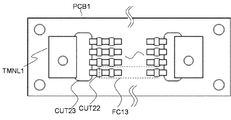
Next, with reference to FIG. 5, a coil device according to a third exemplary embodiment of the present invention will be described in detail. FIG. 5: is the figure which showed typically the structure of the 1st capacitor circuit in the coil apparatus which concerns on 3rd Embodiment of this invention. The configuration of the coil device according to the third embodiment is the same as that of the coil device Lu1 according to the first embodiment. The coil device according to the third embodiment is different from the first embodiment in that the plurality of capacitor elements CAP1 forming the first and second capacitor circuits X10 and X11 (capacitor circuit X1) have different configurations. Since the first capacitor circuit X10 and the second capacitor circuit X11 have the same configuration, only the configuration of the first capacitor circuit X10 will be described here.
第1のキャパシタ回路X10は、第1実施形態と同様、複数のキャパシタ素子CAP1が基板PCB1上に実装されて構成されており、基板PCB1上の一対の接続端子TMNL1間に複数のキャパシタ素子CAP1が直並列に接続されている。ここで、複数のキャパシタ素子CAP1は、一対の接続端子TMNL1間に行列状に整列配置されており、基板PCB1上に設けられた複数の銅箔CUT1により複数のキャパシタ素子CAP1同士が接続されている。具体的には、図5に示されるように、複数の銅箔CUT1は、行方向(横方向)に隣接するキャパシタ素子同士ならびに列方向(縦方向)に隣接するキャパシタ素子同士を接続するとともに、行方向の両端に位置するキャパシタ素子を一対の接続端子TMNL1に接続するように設けられている。これにより、第1のキャパシタ回路X10は、複数のキャパシタ素子CAP1が直並列接続されたキャパシタ群MLCC13を有することとなる。なお、本実施形態では、複数のキャパシタ素子CAP1が1つの基板の片面に実装されているがこれに限られることなく、1つの基板の両面に実装されていてもよく、複数の基板にそれぞれ実装されていてもよい。ここで、複数のキャパシタ素子CAP1が1つの基板の両面あるいは複数の基板にそれぞれ実装されている場合、それぞれの面あるいは基板に実装される複数のキャパシタ素子CAP1がいずれも直並列接続されたキャパシタ群を有すると好ましいが、少なくともいずれかの面あるいは基板に複数のキャパシタ素子CAP1が直並列接続されたキャパシタ群を有するような構成であっても構わない。 Similar to the first embodiment, the first capacitor circuit X10 is configured by mounting a plurality of capacitor elements CAP1 on the board PCB1, and the plurality of capacitor elements CAP1 are provided between the pair of connection terminals TMNL1 on the board PCB1. It is connected in series and parallel. Here, the plurality of capacitor elements CAP1 are arranged in a matrix between the pair of connection terminals TMNL1 and the plurality of capacitor elements CAP1 are connected to each other by the plurality of copper foils CUT1 provided on the substrate PCB1. .. Specifically, as shown in FIG. 5, the plurality of copper foils CUT1 connect capacitor elements adjacent to each other in the row direction (horizontal direction) and capacitor elements adjacent to each other in the column direction (vertical direction), Capacitor elements located at both ends in the row direction are provided so as to be connected to the pair of connection terminals TMNL1. As a result, the first capacitor circuit X10 has the capacitor group MLCC13 in which the plurality of capacitor elements CAP1 are connected in series and parallel. In the present embodiment, the plurality of capacitor elements CAP1 are mounted on one side of one substrate, but the present invention is not limited to this, and may be mounted on both sides of one substrate. It may have been done. Here, when a plurality of capacitor elements CAP1 are mounted on both surfaces of a substrate or on a plurality of substrates, respectively, a capacitor group in which the plurality of capacitor elements CAP1 mounted on the respective surfaces or substrates are connected in series and parallel However, it is also possible to have a configuration having a capacitor group in which a plurality of capacitor elements CAP1 are connected in series and parallel on at least one of the surfaces or the substrate.
本実施形態では、複数のキャパシタ素子CAP1の各々は、積層セラミックコンデンサから構成されている。ここで、積層セラミックコンデンサの最頻の故障モードはショートモードであり、複数のキャパシタ素子CAP1に積層セラミックコンデンサを使用する場合、複数のキャパシタ素子CAP1は、ショート故障によりキャパシタ回路X1の合成静電容量が大きく変化する回路構成であると好ましい。本実施形態では、キャパシタ回路X1は、複数のキャパシタ素子CAP1が直並列接続されたキャパシタ群MLCC13を有するため、このキャパシタ群MLCC13のキャパシタ素子に1つでもショート故障が生じると、キャパシタ回路X1の合成静電容量が大きく変化し、金属部SDと基準電位間の交流電圧も大きく変化する。つまり、キャパシタ回路X1を構成する複数のキャパシタ素子CAP1の故障を確実に検出することができる。 In the present embodiment, each of the plurality of capacitor elements CAP1 is composed of a laminated ceramic capacitor. Here, the most frequent failure mode of the monolithic ceramic capacitor is a short mode, and when a monolithic ceramic capacitor is used for the plurality of capacitor elements CAP1, the plurality of capacitor elements CAP1 are short-circuited and the combined electrostatic capacitance of the capacitor circuit X1. It is preferable that the circuit configuration has a large change. In the present embodiment, the capacitor circuit X1 has the capacitor group MLCC13 in which a plurality of capacitor elements CAP1 are connected in series and parallel. Therefore, when even one short circuit failure occurs in the capacitor group MLCC13, the capacitor circuit X1 is synthesized. The capacitance changes greatly, and the AC voltage between the metal part SD and the reference potential also changes greatly. That is, it is possible to reliably detect the failure of the plurality of capacitor elements CAP1 that form the capacitor circuit X1.
以上のように、本実施形態に係るコイル装置は、複数のキャパシタ素子CAP1の各々は、積層セラミックコンデンサから構成され、キャパシタ回路X1は、複数のキャパシタ素子CAP1が直並列接続されたキャパシタ群MLCC13を有している。この構成により、単一の積層セラミックコンデンサにショート故障が発生した際に、キャパシタ回路X1の静電容量変化が大きくなる。そのため、金属部SDに発生する電圧変化も大きくなり、キャパシタ回路X1を構成する複数のキャパシタ素子CAP1の故障をより確実に検出することができる。 As described above, in the coil device according to the present embodiment, each of the plurality of capacitor elements CAP1 is composed of the laminated ceramic capacitor, and the capacitor circuit X1 includes the capacitor group MLCC13 in which the plurality of capacitor elements CAP1 are connected in series and parallel. Have With this configuration, when a short circuit failure occurs in a single monolithic ceramic capacitor, the capacitance change of the capacitor circuit X1 becomes large. Therefore, the voltage change generated in the metal part SD also becomes large, and the failure of the plurality of capacitor elements CAP1 forming the capacitor circuit X1 can be detected more reliably.
(第4実施形態)
次に、図6を参照して、本発明の第3実施形態に係るコイル装置について詳細に説明する。図6は、本発明の第4実施形態に係るコイル装置における第1のキャパシタ回路の構成を模式的に示した図である。第4実施形態に係るコイル装置が備える構成は、第1実施形態に係るコイル装置Lu1と同様である。第4実施形態に係るコイル装置においては、第1および第2のキャパシタ回路X10,X11(キャパシタ回路X1)を構成する複数のキャパシタ素子CAP1の接続構成が異なる点で第1実施形態と相違する。なお、第1のキャパシタ回路X10と第2のキャパシタ回路X11の構成は同様のため、ここでは第1のキャパシタ回路X10の構成のみ説明する。
(Fourth Embodiment)
Next, with reference to FIG. 6, a coil device according to a third exemplary embodiment of the present invention will be described in detail. FIG. 6 is a diagram schematically showing the configuration of the first capacitor circuit in the coil device according to the fourth embodiment of the present invention. The configuration of the coil device according to the fourth embodiment is similar to that of the coil device Lu1 according to the first embodiment. The coil device according to the fourth embodiment is different from the first embodiment in that the connection configuration of a plurality of capacitor elements CAP1 forming the first and second capacitor circuits X10 and X11 (capacitor circuit X1) is different. Since the first capacitor circuit X10 and the second capacitor circuit X11 have the same configuration, only the configuration of the first capacitor circuit X10 will be described here.
第1のキャパシタ回路X10は、第1実施形態と同様、複数のキャパシタ素子CAP1が基板PCB1上に実装されて構成されており、基板PCB1上の一対の接続端子TMNL1間に複数のキャパシタ素子CAP1が、直列接続されている。ここで、複数のキャパシタ素子CAP1は、一対の接続端子TMNL1間に行列状に整列配置されており、基板PCB1上に設けられた複数の銅箔CUT22および一対の銅箔CUT23により複数のキャパシタ素子CAP1同士が接続されている。具体的には、図6に示されるように、複数の銅箔CUT22は、行方向(横方向)に隣接するキャパシタ素子同士を直列に接続するとともに、一対の銅箔CUT23は、行方向の両端に位置するキャパシタ素子を接続端子TMNL1に接続するように設けられている。但し、本実施形態では、列方向に隣接する複数の銅箔CUT22は、互いに接触しておらず離間して配置され、直接電気的には接続されていない。これにより、第1のキャパシタ回路X10は、複数のキャパシタ素子CAP1が直列に接続されたキャパシタ部FC13を複数有することとなる。なお、本実施形態では、複数のキャパシタ素子CAP1が1つの基板の片面に実装されているがこれに限られることなく、1つの基板の両面に実装されていてもよく、複数の基板にそれぞれ実装されていてもよい。ここで、複数のキャパシタ素子CAP1が1つの基板の両面あるいは複数の基板にそれぞれ実装されている場合、それぞれの面あるいは基板に実装される複数のキャパシタ素子CAP1が直列に接続されたキャパシタ部FC13を複数有すると好ましいが、少なくともいずれかの面あるいは基板に複数のキャパシタ素子CAP1が直列に接続されたキャパシタ部FC13を複数有するような構成であっても構わない。 Similar to the first embodiment, the first capacitor circuit X10 is configured by mounting a plurality of capacitor elements CAP1 on the board PCB1, and the plurality of capacitor elements CAP1 are provided between the pair of connection terminals TMNL1 on the board PCB1. , Connected in series. Here, the plurality of capacitor elements CAP1 are arranged in a matrix between the pair of connection terminals TMNL1, and the plurality of capacitor elements CAP1 are provided by the plurality of copper foils CUT22 and the pair of copper foils CUT23 provided on the substrate PCB1. They are connected to each other. Specifically, as shown in FIG. 6, the plurality of copper foils CUT22 connect capacitor elements adjacent to each other in the row direction (horizontal direction) in series, and the pair of copper foils CUT23 have both ends in the row direction. The capacitor element located at is connected to the connection terminal TMNL1. However, in the present embodiment, the plurality of copper foils CUT 22 adjacent to each other in the column direction are not in contact with each other and are arranged apart from each other, and are not directly electrically connected. As a result, the first capacitor circuit X10 has a plurality of capacitor sections FC13 in which a plurality of capacitor elements CAP1 are connected in series. In the present embodiment, the plurality of capacitor elements CAP1 are mounted on one side of one substrate, but the present invention is not limited to this, and may be mounted on both sides of one substrate. It may have been done. Here, when a plurality of capacitor elements CAP1 are mounted on both surfaces of a substrate or on a plurality of substrates, respectively, a capacitor section FC13 in which the plurality of capacitor elements CAP1 mounted on each surface or substrate are connected in series is used. Although it is preferable to have a plurality of capacitors, at least one surface or substrate may have a plurality of capacitor parts FC13 in which a plurality of capacitor elements CAP1 are connected in series.
本実施形態では、複数のキャパシタ素子CAP1の各々は、フィルムコンデンサから構成されている。ここで、フィルムコンデンサの最頻の故障モードはオープンモードであり、複数のキャパシタ素子CAP1にフィルムコンデンサを使用する場合、複数のキャパシタ素子CAP1は、オープン故障によりキャパシタ回路X1の合成静電容量が大きく変化する回路構成であると好ましい。本実施形態では、キャパシタ回路X1は、複数のキャパシタ素子が直列に接続されたキャパシタ部FC13を複数有するため、このキャパシタ部FC13のキャパシタ素子に1つでもオープン故障が生じると、キャパシタ回路X1の合成静電容量が大きく変化し、金属部SDと基準電位間の交流電圧も大きく変化する。つまり、キャパシタ回路X1を構成する複数のキャパシタ素子CAP1の故障を確実に検出することができる。 In the present embodiment, each of the plurality of capacitor elements CAP1 is composed of a film capacitor. Here, the most frequent failure mode of the film capacitor is the open mode, and when a film capacitor is used for the plurality of capacitor elements CAP1, the plurality of capacitor elements CAP1 have a large combined capacitance of the capacitor circuit X1 due to the open failure. A circuit configuration that changes is preferable. In the present embodiment, the capacitor circuit X1 has a plurality of capacitor sections FC13 in which a plurality of capacitor elements are connected in series. Therefore, when even one open circuit failure occurs in the capacitor section FC13, the capacitor circuit X1 is combined. The capacitance changes greatly, and the AC voltage between the metal part SD and the reference potential also changes greatly. That is, it is possible to reliably detect the failure of the plurality of capacitor elements CAP1 that form the capacitor circuit X1.
以上のように、本実施形態に係るコイル装置は、複数のキャパシタ素子CAP1の各々は、フィルムコンデンサから構成され、キャパシタ回路X1は、複数のキャパシタ素子CAP1が直列に接続されたキャパシタ部FC13を複数有している。この構成により、単一のフィルムコンデンサにオープン故障が発生した際に、キャパシタ回路X1の静電容量変化が大きくなる。そのため、金属部SDに発生する電圧もしくは電流変化も大きくなり、キャパシタ回路X1を構成する複数のキャパシタ素子CAP1の故障をより確実に検出することができる。 As described above, in the coil device according to the present embodiment, each of the plurality of capacitor elements CAP1 is formed of a film capacitor, and the capacitor circuit X1 includes the plurality of capacitor parts FC13 in which the plurality of capacitor elements CAP1 are connected in series. Have With this configuration, when an open failure occurs in a single film capacitor, the capacitance change of the capacitor circuit X1 becomes large. Therefore, the change in the voltage or current generated in the metal part SD also becomes large, and the failure of the plurality of capacitor elements CAP1 forming the capacitor circuit X1 can be detected more reliably.
(第5実施形態)
図7を参照して、本発明の第5実施形態に係るコイル装置Lu5の構成について詳細に説明する。図7は、本発明の第5実施形態に係るコイル装置の回路構成を模式的に示した図である。コイル装置Lu5は、図7に示されるように、電力伝送用コイルL1と、金属部SDと、キャパシタ回路X5と、計測部VSG1を有する。電力伝送用コイルL1、金属部SD、計測部VSG1の構成は、第1実施形態に係るコイル装置Lu1と同様である。第5実施形態に係るコイル装置Lu5は、キャパシタ回路X1に代えてキャパシタ回路X5を備えている点において、第1実施形態と相違する。以下、第1実施形態と異なる点を中心に説明する。
(Fifth Embodiment)
The configuration of the coil device Lu5 according to the fifth embodiment of the present invention will be described in detail with reference to FIG. FIG. 7 is a diagram schematically showing the circuit configuration of a coil device according to the fifth embodiment of the present invention. As shown in FIG. 7, the coil device Lu5 includes a power transmission coil L1, a metal part SD, a capacitor circuit X5, and a measuring part VSG1. The configurations of the power transmission coil L1, the metal part SD, and the measuring part VSG1 are the same as those of the coil device Lu1 according to the first embodiment. The coil device Lu5 according to the fifth embodiment differs from that of the first embodiment in that the coil device Lu5 includes a capacitor circuit X5 instead of the capacitor circuit X1. Hereinafter, differences from the first embodiment will be mainly described.
キャパシタ回路X5は、キャパシタ回路X1と同様、電力伝送用コイルL1に接続され、電力伝送用コイルL1と共振回路を形成している。このキャパシタ回路X5は、共振回路の共振周波数を調整する機能を有する。本実施形態では、キャパシタ回路X5は、第1のキャパシタ回路X50と、第2のキャパシタ回路X51と、を有する。 Like the capacitor circuit X1, the capacitor circuit X5 is connected to the power transmission coil L1 and forms a resonance circuit with the power transmission coil L1. The capacitor circuit X5 has a function of adjusting the resonance frequency of the resonance circuit. In the present embodiment, the capacitor circuit X5 has a first capacitor circuit X50 and a second capacitor circuit X51.
第1のキャパシタ回路X50は、一方端が電力伝送用コイルL1の一方端に接続され、第2のキャパシタ回路X51は、一方端が電力伝送用コイルL1の他方端に接続されている。この点は、第1実施形態に係る第1のキャパシタ回路X10及び第2のキャパシタ回路X11と同様である。第1実施形態と異なる点は、第1のキャパシタ回路X50の他方端と第2のキャパシタ回路X51の他方端が互いに接続されており、第1のキャパシタ回路X50と第2のキャパシタ回路X51の接続中点が抵抗RG55を介して基準電位に接続されている点である。つまり、本実施形態では、第1のキャパシタ回路X50及び第2のキャパシタ回路X51は、電力伝送用コイルL1に並列に接続されている。なお、第1及び第2のキャパシタ回路X50,X51が有する複数のキャパシタ素子の構成は、第1実施形態における第1及び第2のキャパシタ回路X10,X11が有する複数のキャパシタ素子CAP1と同様のため説明は省略する。また、第1のキャパシタ回路X50の合成静電容量と、第2のキャパシタ回路X51の合成静電容量が略等しく構成されていると好ましい。この場合、金属部SDと基準電位間の交流電圧もしくは交流電流が低くなり、計測部VSG1の計測負荷が低減できる。 One end of the first capacitor circuit X50 is connected to one end of the power transmission coil L1, and one end of the second capacitor circuit X51 is connected to the other end of the power transmission coil L1. This point is the same as the first capacitor circuit X10 and the second capacitor circuit X11 according to the first embodiment. The difference from the first embodiment is that the other end of the first capacitor circuit X50 and the other end of the second capacitor circuit X51 are connected to each other, and the connection between the first capacitor circuit X50 and the second capacitor circuit X51. The middle point is the point connected to the reference potential via the resistor RG55. That is, in the present embodiment, the first capacitor circuit X50 and the second capacitor circuit X51 are connected in parallel to the power transmission coil L1. The configuration of the plurality of capacitor elements included in the first and second capacitor circuits X50 and X51 is similar to that of the plurality of capacitor elements CAP1 included in the first and second capacitor circuits X10 and X11 in the first embodiment. The description is omitted. Further, it is preferable that the combined capacitance of the first capacitor circuit X50 and the combined capacitance of the second capacitor circuit X51 are substantially equal. In this case, the AC voltage or the AC current between the metal part SD and the reference potential becomes low, and the measuring load of the measuring part VSG1 can be reduced.
上述したように、本実施形態は、キャパシタ回路X5が電力伝送用コイルL1に対して並列に接続されている点を除けば、第1実施形態と同一の形態である。すなわち、本実施形態に係るコイル装置Lu5は、電力伝送用コイルL1に近接して配置される導電性の金属部SDと、金属部SDに発生する電圧もしくは電流を計測する計測部VSG1を備えているため、キャパシタ回路X5を構成する複数のキャパシタ素子にショート故障またはオープン故障が発生した際の微小な容量変化に応じて、電力伝送用コイルL1と金属部SDとの間に生じる寄生容量C12,C13を介して発生する金属部SDの電圧もしくは電流の変化を、計測部VSG1により検知できる。したがって、キャパシタ回路X5を構成する複数のキャパシタ素子のいずれかにショート故障またはオープン故障が生じたことを確実に検出することができる。 As described above, the present embodiment is the same as the first embodiment except that the capacitor circuit X5 is connected in parallel to the power transmission coil L1. That is, the coil device Lu5 according to the present embodiment includes a conductive metal part SD arranged in the vicinity of the power transmission coil L1 and a measuring part VSG1 for measuring the voltage or current generated in the metal part SD. Therefore, the parasitic capacitance C12 generated between the power transmission coil L1 and the metal part SD in accordance with a minute capacitance change when a short circuit failure or an open circuit failure occurs in the plurality of capacitor elements forming the capacitor circuit X5, The change in the voltage or current of the metal part SD generated via C13 can be detected by the measuring part VSG1. Therefore, it is possible to reliably detect that a short circuit failure or an open failure has occurred in any of the plurality of capacitor elements that form the capacitor circuit X5.
なお、第1〜第4実施形態では、キャパシタ回路X1が電力伝送用コイルL1に対して直列に接続されている形態、第5実施形態では、キャパシタ回路X5が電力伝送用コイルL1に対して並列に接続されている形態を説明したが、電力伝送用コイルL1とともに共振回路を形成するキャパシタ回路が、電力伝送用コイルL1に対して直列及び並列に接続されている場合であっても、上述の実施形態と同様の作用効果が得られる。 In the first to fourth embodiments, the capacitor circuit X1 is connected in series to the power transmission coil L1, and in the fifth embodiment, the capacitor circuit X5 is parallel to the power transmission coil L1. However, even if the capacitor circuit forming the resonance circuit together with the power transmission coil L1 is connected in series and in parallel to the power transmission coil L1, The same effect as that of the embodiment can be obtained.
以下、上述の実施形態による、キャパシタ回路を構成する複数のキャパシタ素子のいずれかがショート故障した際に、確実に検出できることを実施例1〜3によって具体的に示す。 Hereinafter, it will be concretely shown by Examples 1 to 3 that when one of the plurality of capacitor elements forming the capacitor circuit according to the above-described embodiment is short-circuited, it can be reliably detected.
実施例1〜3として、上述した第3実施形態に係るコイル装置を給電コイル装置130および受電コイル装置210に適用したワイヤレス電力伝送装置S1を用いた。各実施例における、給電コイル装置130の給電コイルのインダクタンスを600uHとし、給電コイル装置130の金属部SDを厚さ2mmのアルミニウムとし、給電コイル装置130の第1および第2のキャパシタ回路X10、X11を構成する複数のキャパシタ素子を、単一の静電容量が33nFの積層セラミックコンデンサとし、給電コイル装置130の第1および第2のキャパシタ回路X10、X11の合成静電容量をそれぞれ12.8nFとし、受電コイル装置210の受電コイルのインダクタンスを85uHとし、受電コイル装置210の金属部SDを厚さ2mmのアルミニウムとし、受電コイル装置210の第1および第2のキャパシタ回路X10,X11を構成する複数のキャパシタ素子を、単一の静電容量が33nFの積層セラミックコンデンサとし、受電コイル装置210の第1および第2のキャパシタ回路X10,X11の合成静電容量をそれぞれ90nFとした。ここで、キャパシタ素子の故障個所をよりわかりやすく説明するため、各実施例における給電コイル装置130の第1のキャパシタ回路X10の構成を図8に示す。図8は、各実施例における給電コイル装置の第1のキャパシタ回路の構成を模式的に示した図である。図8に示すように、各実施例における給電コイル装置130の第1のキャパシタ回路X10は、複数のキャパシタ素子CAP1が、基板PCB上の一対の接続端子TMNL1間に行列状に整列配置(18直列7並列)され、複数の銅箔CUT1により直並列接続されたキャパシタ群MLCC13を構成している。図8では、このキャパシタ群MLCC13に対して、直列方向に番号N1〜N18により直列番地を表示し、並列方向に番号M1〜M7により並列番地を表示している。例えば、キャパシタ群MLCC13の直列番地がN2、並列番地がM2で示される積層セラミックコンデンサMLCCS1にショート故障が生じると、N2で示される直列番地における、M1およびM3からM7の並列番地で示される積層セラミックコンデンサがキャパシタ素子として機能しなくなる。すなわち、単一の積層セラミックコンデンサのショート故障により大きな静電容量変化が生じることとなる。
As Examples 1 to 3, the wireless power transmission device S1 in which the coil device according to the third embodiment described above is applied to the power
また、各実施例における負荷RLを37Ωとし、電力変換回路120から給電コイル装置130の給電コイルへ供給される交流電圧を400Vとし、負荷RLへの伝送電力が3.3kWとなるように、交流電圧の周波数を調整した。さらに、各実施例における計測部VSG1の一端を金属部SDに接続し、他端を基準電位に接続した。
In addition, the load RL in each example is set to 37Ω, the AC voltage supplied from the
これら実施例1〜3について、ワイヤレス給電装置100からワイヤレス受電装置200への電力伝送を開始し、計測部VSG1により金属部SDに発生した交流電圧実効値を計測するとそれぞれ0.2Vであった。つまり、この交流電圧実効値が複数のキャパシタ素子に故障がない状態の基準となる電圧値である。
In each of Examples 1 to 3, when the power transmission from the wireless
続いて、ワイヤレス給電装置100からワイヤレス受電装置200への電力伝送を停止し、実施例1では第1のキャパシタ回路X10の直列番地がN2、並列番地がM2で示される積層セラミックコンデンサをショートさせ、実施例2では第1のキャパシタ回路X10の直列番地がN2、並列番地がM2で示される積層セラミックコンデンサと直列番地がN3、並列番地がM2で示される積層セラミックコンデンサをショートさせ、実施例3では第1のキャパシタ回路X10の直列番地がN2、並列番地がM2で示される積層セラミックコンデンサと直列番地がN3、並列番地がM2で示される積層セラミックコンデンサと直列番地がN4と並列番地がM2で示される積層セラミックコンデンサをショートさせた。この状態において、再度ワイヤレス給電装置100からワイヤレス受電装置200への電力伝送を開始し、計測部VSG1により金属部SDに発生した交流電圧実効値を計測した。各実施例の計測結果を表1に示す
Then, the power transmission from the wireless

表1に示すように、実施例1では、複数のキャパシタ素子の故障数が1つにも関わらず、第1のキャパシタ回路X10の合成静電容量が13.6nFと大きく変化し、計測部VSG1で計測された金属部SDに発生した交流電圧実効値が26.5Vとなった。つまり、金属部SDに発生する交流電圧実効値が、複数のキャパシタ素子に故障がない状態の0.2Vから26V以上変化したため、単一の積層セラミックコンデンサのショート故障を確実に検出できることが確認できた。実施例2では、第1のキャパシタ回路X10の合成静電容量が14.4nFと実施例1に比べて一層大きく変化し、計測部VSG1で計測された金属部SDに発生した交流電圧実効値が62Vとなった。つまり、金属部SDに発生する交流電圧実効値が、複数のキャパシタ素子に故障がない状態の0.2Vから61V以上変化したため、わずか2つの積層セラミックコンデンサのショート故障を確実に検出できることが確認できた。実施例3では、第1のキャパシタ回路X10の合成静電容量が15.4nFと実施例1および実施例2に比べてより一層大きく変化し、計測部VSG1で計測された金属部SDに発生した交流電圧実効値が105.7Vとなった。つまり、金属部SDに発生する交流電圧実効値が、複数のキャパシタ素子に故障がない状態の0.2Vから105V以上変化したため、わずか3つの積層セラミックコンデンサのショート故障を確実に検出できることが確認できた。以上のことから、本実施形態によってキャパシタ回路を構成する複数のキャパシタ素子のショート故障を確実に検出できることが確認された。なお、本実施例では、複数のキャパシタ素子のショート故障を検出できることを示したが、オープン故障であっても、その故障に基づく静電容量の変化が金属部の電位変化として現れるため、その故障を確実に検出できることはいうまでもない。 As shown in Table 1, in the first embodiment, the combined capacitance of the first capacitor circuit X10 greatly changes to 13.6 nF even though the number of failures of the plurality of capacitor elements is 1, and the measurement unit VSG1 The effective value of the AC voltage generated in the metal part SD measured at 26.5V was 26.5V. That is, since the effective value of the AC voltage generated in the metal part SD has changed by 0.2 V or more from 0.2 V when there is no failure in the plurality of capacitor elements, it can be confirmed that the short-circuit failure of the single multilayer ceramic capacitor can be reliably detected. It was In the second embodiment, the combined capacitance of the first capacitor circuit X10 is 14.4 nF, which is much larger than that in the first embodiment, and the effective value of the AC voltage generated in the metal part SD measured by the measuring unit VSG1 is It became 62V. That is, since the effective value of the AC voltage generated in the metal part SD has changed from 0.2 V when there is no failure in the plurality of capacitor elements by 61 V or more, it can be confirmed that a short circuit failure of only two multilayer ceramic capacitors can be reliably detected. It was In Example 3, the combined capacitance of the first capacitor circuit X10 was 15.4 nF, which was much larger than those in Examples 1 and 2 and occurred in the metal part SD measured by the measuring unit VSG1. The AC voltage effective value was 105.7V. That is, since the effective value of the AC voltage generated in the metal part SD has changed from 0.2 V when there is no failure in the plurality of capacitor elements by 105 V or more, it can be confirmed that a short circuit failure of only three multilayer ceramic capacitors can be reliably detected. It was From the above, it was confirmed that a short circuit failure of a plurality of capacitor elements forming a capacitor circuit can be reliably detected by this embodiment. In this example, it was shown that a short-circuit failure of a plurality of capacitor elements can be detected. However, even if the failure is an open failure, the change in capacitance due to the failure appears as a change in the potential of the metal part. Needless to say, can be reliably detected.
100…ワイヤレス給電装置、110…電源、120…電力変換回路、121…電力変換部、122…スイッチ駆動部、130…給電コイル装置、200…ワイヤレス受電装置、210…受電コイル装置、220…整流部、C0…平滑コンデンサ、D1〜D4…ダイオード、RL…負荷、S1…ワイヤレス電力伝送装置、SG1〜SG4…SW制御信号、SW1〜SW4…スイッチング素子、GND1…グランド、FGND1…フレームグランド、RG1〜RG4…分圧抵抗、Lu1…コイル装置、L1…電力伝送用コイル、C12,C13…寄生容量、X1,X10,X11…キャパシタ回路、SD…金属部、VSG1…計測部、PCBX10,PCB1…基板、CAP1…キャパシタ素子、CUT,CUT1,CUT22,CUT23…銅箔、TMNLX10,TMNL1…端子、VSGR1…抵抗、VSGM1…交流電圧計、AD1…アナログデジタル変換部、COM1…無線通信部、MLCC13…キャパシタ群、FC13…キャパシタ部。 100... Wireless power feeding device, 110... Power source, 120... Power conversion circuit, 121... Power conversion unit, 122... Switch driving unit, 130... Power feeding coil device, 200... Wireless power receiving device, 210... Power receiving coil device, 220... Rectifying unit , C0... Smoothing capacitor, D1 to D4... Diode, RL... Load, S1... Wireless power transmission device, SG1 to SG4... SW control signal, SW1 to SW4... Switching element, GND1... Ground, FGND1... Frame ground, RG1 to RG4 ... voltage dividing resistance, Lu1... coil device, L1... power transmission coil, C12, C13... parasitic capacitance, X1, X10, X11... capacitor circuit, SD... metal part, VSG1... measurement part, PCBX10, PCB1... substrate, CAP1 Capacitor element, CUT, CUT1, CUT22, CUT23... Copper foil, TMNLX10, TMNL1... Terminal, VSGR1... Resistor, VSGM1... AC voltmeter, AD1... Analog-to-digital converter, COM1... Wireless communication section, MLCC13... Capacitor group, FC13 … Capacitor section.
Claims (4)
前記電力伝送用コイルに接続され、複数のキャパシタ素子を有するキャパシタ回路と、
前記電力伝送用コイルと近接して配置される導電性の金属部と、
前記金属部に発生する電圧もしくは、電流を計測する計測部を備え、
前記キャパシタ回路は、前記電力伝送用コイルの一方端に接続される第1のキャパシタ回路と、前記電力伝送用コイルの他方端に接続される第2のキャパシタ回路を有し、
前記第1のキャパシタ回路の合成静電容量は、前記第2のキャパシタ回路の合成静電容量と略等しいことを特徴とするコイル装置。 Power transmission coil,
A capacitor circuit having a plurality of capacitor elements, which is connected to the power transmission coil;
A conductive metal portion arranged in proximity to the power transmission coil,
The voltage generated in the metal part, or equipped with a measuring unit for measuring the current ,
The capacitor circuit has a first capacitor circuit connected to one end of the power transmission coil and a second capacitor circuit connected to the other end of the power transmission coil,
The coil device , wherein the combined capacitance of the first capacitor circuit is substantially equal to the combined capacitance of the second capacitor circuit .
前記キャパシタ回路は、前記複数のキャパシタ素子が直並列接続されたキャパシタ群を有することを特徴とする請求項1に記載のコイル装置。 Each of the plurality of capacitor elements is composed of a laminated ceramic capacitor,
The coil device according to claim 1 , wherein the capacitor circuit includes a capacitor group in which the plurality of capacitor elements are connected in series and parallel.
前記キャパシタ回路は、前記複数のキャパシタ素子が直列接続されたキャパシタ部を複数有することを特徴とする請求項1に記載のコイル装置。 Each of the plurality of capacitor elements is composed of a film capacitor,
The coil device according to claim 1 , wherein the capacitor circuit has a plurality of capacitor units in which the plurality of capacitor elements are connected in series.
受電コイル装置を含むワイヤレス受電装置を備え、
前記給電コイル装置と、前記受電コイル装置の少なくとも一方が、請求項1〜3のいずれか一項に記載のコイル装置であることを特徴とするワイヤレス電力伝送装置。 A wireless power supply device including a power supply coil device;
A wireless power receiving device including a power receiving coil device is provided,
Wherein the feeding coil device, at least one of the power receiving coil system, the wireless power transmission apparatus which is a coil apparatus according to any one of claims 1-3.
Priority Applications (3)
| Application Number | Priority Date | Filing Date | Title |
|---|---|---|---|
| CN201610798136.0A CN106487100B (en) | 2015-09-02 | 2016-08-31 | Coil device and wireless power transmission device |
| DE102016116342.2A DE102016116342A1 (en) | 2015-09-02 | 2016-09-01 | COIL DEVICE AND WIRELESS POWER TRANSMISSION DEVICE |
| US15/254,331 US10284017B2 (en) | 2015-09-02 | 2016-09-01 | Coil device and wireless power transmission device |
Applications Claiming Priority (2)
| Application Number | Priority Date | Filing Date | Title |
|---|---|---|---|
| JP2015172823 | 2015-09-02 | ||
| JP2015172823 | 2015-09-02 |
Publications (2)
| Publication Number | Publication Date |
|---|---|
| JP2017051084A JP2017051084A (en) | 2017-03-09 |
| JP6747149B2 true JP6747149B2 (en) | 2020-08-26 |
Family
ID=58280542
Family Applications (1)
| Application Number | Title | Priority Date | Filing Date |
|---|---|---|---|
| JP2016152550A Active JP6747149B2 (en) | 2015-09-02 | 2016-08-03 | Coil device and wireless power transmission device |
Country Status (1)
| Country | Link |
|---|---|
| JP (1) | JP6747149B2 (en) |
Families Citing this family (1)
| Publication number | Priority date | Publication date | Assignee | Title |
|---|---|---|---|---|
| JP2019087592A (en) | 2017-11-06 | 2019-06-06 | Tdk株式会社 | Capacitor module, resonator, wireless power transmission device, wireless power reception device, and wireless power transmission system |
Family Cites Families (6)
| Publication number | Priority date | Publication date | Assignee | Title |
|---|---|---|---|---|
| JP2009071960A (en) * | 2007-09-12 | 2009-04-02 | Meleagros Corp | Power transmitter, transmission device of power transmitter, reception device of power transmitter, and method and device for evaluating performance of capacitor for high frequency power circuit |
| EP2775590B1 (en) * | 2011-11-04 | 2018-07-11 | Panasonic Intellectual Property Management Co., Ltd. | Coil unit and contactless electric power transmission device |
| JP5293851B2 (en) * | 2012-02-20 | 2013-09-18 | 住友電気工業株式会社 | Coil unit and non-contact power supply system |
| JP6102242B2 (en) * | 2012-12-20 | 2017-03-29 | Tdk株式会社 | Wireless power supply device and wireless power transmission device |
| JP2014217199A (en) * | 2013-04-26 | 2014-11-17 | 株式会社ノーリツ | Power conversion device |
| US9562955B2 (en) * | 2014-01-20 | 2017-02-07 | Qualcomm Incorporated | Methods and apparatus for magnetic field strength measurement |
-
2016
- 2016-08-03 JP JP2016152550A patent/JP6747149B2/en active Active
Also Published As
| Publication number | Publication date |
|---|---|
| JP2017051084A (en) | 2017-03-09 |
Similar Documents
| Publication | Publication Date | Title |
|---|---|---|
| US10284017B2 (en) | Coil device and wireless power transmission device | |
| EP3282539B1 (en) | Power transmission device, vehicle equipped with power transmission device, and wireless power transmission system | |
| JP4735469B2 (en) | Switching power supply | |
| EP3016231B1 (en) | Power transmission device, vehicle equipped with power transmission device, and wireless power transmission system | |
| JP6667163B2 (en) | Power transmission device, vehicle equipped with power transmission device, and wireless power transmission system | |
| CN103190063A (en) | Circuit arrangement and method for reducing common-mode noise in a switched-mode power supply, and a switched-mode power supply | |
| WO2016125725A1 (en) | Electric current detection element and electrical power transmission system | |
| JP2016039644A (en) | Power transmission device and radio power transmission system | |
| JP6747149B2 (en) | Coil device and wireless power transmission device | |
| JP5240529B2 (en) | Switching power supply | |
| JP2014055831A (en) | Measuring apparatus | |
| JP2007157985A (en) | Non-contact power supply system | |
| KR101629964B1 (en) | Power semiconductor module with control functionality and integrated transformer | |
| JP2021019421A (en) | Current detector | |
| JP6361825B2 (en) | Current detection element, power transmission device and power transmission system | |
| WO2021131607A1 (en) | Foreign object detection device, power transmission device, power reception device, and power transmission system | |
| CN209199779U (en) | Electronic component, frequency converter and inverter | |
| JP5911441B2 (en) | DC-DC converter transformer wiring structure | |
| WO2013145080A1 (en) | Short circuit testing device and short circuit testing method | |
| JP2016119755A (en) | Detection coil, power supply coil and power reception coil | |
| US9991749B2 (en) | Coil unit, wireless power feeding device, wireless power receiving device, and wireless power transmission device | |
| JP6304276B2 (en) | Coil unit, wireless power feeding device, wireless power receiving device, and wireless power transmission device | |
| JP6179621B2 (en) | Coil unit, wireless power feeding device, wireless power receiving device, and wireless power transmission device | |
| US9935500B2 (en) | Coil unit, wireless power feeding device, wireless power receiving device, and wireless power transmission device | |
| CN109346323A (en) | Electronic component, frequency converter and inverter |
Legal Events
| Date | Code | Title | Description |
|---|---|---|---|
| A621 | Written request for application examination |
Free format text: JAPANESE INTERMEDIATE CODE: A621 Effective date: 20190327 |
|
| A977 | Report on retrieval |
Free format text: JAPANESE INTERMEDIATE CODE: A971007 Effective date: 20200220 |
|
| A131 | Notification of reasons for refusal |
Free format text: JAPANESE INTERMEDIATE CODE: A131 Effective date: 20200310 |
|
| A521 | Written amendment |
Free format text: JAPANESE INTERMEDIATE CODE: A523 Effective date: 20200507 |
|
| TRDD | Decision of grant or rejection written | ||
| A01 | Written decision to grant a patent or to grant a registration (utility model) |
Free format text: JAPANESE INTERMEDIATE CODE: A01 Effective date: 20200707 |
|
| A61 | First payment of annual fees (during grant procedure) |
Free format text: JAPANESE INTERMEDIATE CODE: A61 Effective date: 20200720 |
|
| R150 | Certificate of patent or registration of utility model |
Ref document number: 6747149 Country of ref document: JP Free format text: JAPANESE INTERMEDIATE CODE: R150 |