WO2020246245A1 - 光偏向器及び製造方法 - Google Patents
光偏向器及び製造方法 Download PDFInfo
- Publication number
- WO2020246245A1 WO2020246245A1 PCT/JP2020/019976 JP2020019976W WO2020246245A1 WO 2020246245 A1 WO2020246245 A1 WO 2020246245A1 JP 2020019976 W JP2020019976 W JP 2020019976W WO 2020246245 A1 WO2020246245 A1 WO 2020246245A1
- Authority
- WO
- WIPO (PCT)
- Prior art keywords
- torsion bar
- optical deflector
- swell
- mirror
- piezoelectric actuator
- Prior art date
- Legal status (The legal status is an assumption and is not a legal conclusion. Google has not performed a legal analysis and makes no representation as to the accuracy of the status listed.)
- Ceased
Links
Images


Classifications
-
- G—PHYSICS
- G02—OPTICS
- G02B—OPTICAL ELEMENTS, SYSTEMS OR APPARATUS
- G02B26/00—Optical devices or arrangements for the control of light using movable or deformable optical elements
- G02B26/08—Optical devices or arrangements for the control of light using movable or deformable optical elements for controlling the direction of light
- G02B26/0816—Optical devices or arrangements for the control of light using movable or deformable optical elements for controlling the direction of light by means of one or more reflecting elements
- G02B26/0833—Optical devices or arrangements for the control of light using movable or deformable optical elements for controlling the direction of light by means of one or more reflecting elements the reflecting element being a micromechanical device, e.g. a MEMS mirror, DMD
- G02B26/0858—Optical devices or arrangements for the control of light using movable or deformable optical elements for controlling the direction of light by means of one or more reflecting elements the reflecting element being a micromechanical device, e.g. a MEMS mirror, DMD the reflecting means being moved or deformed by piezoelectric means
-
- H—ELECTRICITY
- H02—GENERATION; CONVERSION OR DISTRIBUTION OF ELECTRIC POWER
- H02N—ELECTRIC MACHINES NOT OTHERWISE PROVIDED FOR
- H02N2/00—Electric machines in general using piezoelectric effect, electrostriction or magnetostriction
- H02N2/02—Electric machines in general using piezoelectric effect, electrostriction or magnetostriction producing linear motion, e.g. actuators; Linear positioners ; Linear motors
- H02N2/028—Electric machines in general using piezoelectric effect, electrostriction or magnetostriction producing linear motion, e.g. actuators; Linear positioners ; Linear motors along multiple or arbitrary translation directions, e.g. XYZ stages
-
- H—ELECTRICITY
- H02—GENERATION; CONVERSION OR DISTRIBUTION OF ELECTRIC POWER
- H02N—ELECTRIC MACHINES NOT OTHERWISE PROVIDED FOR
- H02N2/00—Electric machines in general using piezoelectric effect, electrostriction or magnetostriction
- H02N2/22—Methods relating to manufacturing, e.g. assembling, calibration
-
- G—PHYSICS
- G02—OPTICS
- G02B—OPTICAL ELEMENTS, SYSTEMS OR APPARATUS
- G02B26/00—Optical devices or arrangements for the control of light using movable or deformable optical elements
- G02B26/08—Optical devices or arrangements for the control of light using movable or deformable optical elements for controlling the direction of light
- G02B26/10—Scanning systems
- G02B26/105—Scanning systems with one or more pivoting mirrors or galvano-mirrors
Definitions
- the present invention relates to a MEMS optical deflector and a method for manufacturing the same.
- a piezoelectric MEMS optical deflector is known (example: Patent Document 1).
- the joint edge between the mirror portion and the torsion bar is formed by an R portion that is dented inward.
- a SOI (Silicon on Insulator) wafer is used as the substrate for a general piezoelectric MEMS optical deflector.
- the surface index of the main surface is (100) or (110).
- the optical deflector is manufactured by adjusting the crystal orientation of the torsion bar in the axial direction to ⁇ 100>.
- the axial crystal orientation of the torsion bar is set to ⁇ 100>
- An object of the present invention is to provide an optical deflector capable of suppressing cleavage of an R portion provided at a coupling edge portion of a torsion bar and a method for manufacturing the same.
- the optical deflector of the present invention A mirror unit that can reciprocate around a predetermined rotation axis, A pair of torsion bars extending from both sides of the mirror portion along the rotation axis of the mirror portion, A frame portion surrounding the mirror portion and the pair of torsion bars, and a frame portion.
- a plurality of piezoelectric actuators that are interposed between each torsion bar and the frame portion to twist and vibrate each torsion bar around the rotation axis to reciprocate the mirror portion around the rotation axis.
- a first R portion formed by a cylindrical curved surface dented inward at a joint edge portion between each torsion bar and the mirror portion
- a second R portion formed by a cylindrical curved surface dented inward at a coupling edge portion between each piezoelectric actuator on the side facing the mirror portion and each torsion bar
- the mirror portion, the torsion bar, and the substrate layer of the piezoelectric actuator are made of a common silicon single crystal layer.
- the surface index of the main surface of the silicon single crystal layer is one of (100) and (110).
- the axial direction of the torsion bar is ⁇ 100> of the crystal orientation of the silicon single crystal layer.
- At least one predetermined portion of the first R portion and the second R portion is formed so that the unevenness with respect to the cylindrical curved surface is 600 nm or less.
- At least one predetermined portion of the first R portion and the second R portion has irregularities within 600 nm with respect to the cylindrical curved surface. As a result, at least one cleavage can be suppressed.
- both ends of the predetermined portion are set outside both ends of the central divided portion when the cylindrical curved surface is divided into three equal parts.
- the cleavage direction in the first R portion and the second R portion exists in the central divided portion when the cylindrical curved surface is divided into three equal parts. To do. According to this configuration, it is possible to guarantee the suppression of cleavage in the range including the cleavage direction in at least one of the first R portion and the second R portion.
- the contour line when at least one of them is cut by a plane parallel to the main surface is defined as a swell curve.
- An average line by the least squares method is set for the swell curve, The section between the adjacent summits on the swell curve is the period.
- the distance from the average line at each position on the swell curve is defined as the amount of swell.
- the difference between the maximum swell amount and the minimum swell amount of each cycle is 600 nm or less for all the cycles included in the predetermined portion.
- the amount of swell in the predetermined portion can be suppressed, and the cleavage of the first R portion and the second R portion can be suppressed.
- the plane is at least one of the surfaces.
- the surfaces of the 1st R part and the 2nd R part exist in a shallow place from the surface of the light deflector. According to this configuration, the contour lines of the first R portion and the second R portion can be easily detected.
- At least one of them is the second R part.
- the torsion bar receives the torsional force around the rotation axis from the piezoelectric actuator and transmits it to the mirror part. Therefore, during the operation of the optical deflector, a stronger torsional force is applied to the second R portion than to the first R portion.
- the life of the torsion bar can be extended by giving priority to the first R portion over the second R portion and suppressing unevenness.
- the manufacturing method of the present invention A coating step of coating the surface of a substrate containing an active layer of a silicon single crystal whose main surface index is one of (100) and (110) with a photoresist film having a thickness of 5 ⁇ m or more and 10 ⁇ m or less.
- the surface side of the substrate after the coating step via a photomask including contour patterns including contours of the mirror portion, the torsion bar, the piezoelectric actuator, the first R portion and the second R portion of the light deflector.
- the exposure process to expose A contour forming step of etching the surface side of the substrate to form contours of the mirror portion, the torsion bar, the piezoelectric actuator, the first R portion and the second R portion of the optical deflector on the active layer.
- the amount of undulation of the curved surfaces of the first R portion and the second R portion can be guaranteed within 600 nm, and the cleavage of the R portion of the joint portion of the torsion bar can be suppressed.
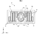
- FIG. 1 is a front view (viewed from the front side) of the MEMS optical deflector 10.
- the optical deflector 10 includes a mirror portion 11, torsion bars 12a, 12b, inner piezoelectric actuators 13a, 13b, a movable frame portion 14, outer piezoelectric actuators 15a, 15b, and a fixed frame portion 16 as main elements.
- a three-axis coordinate system including an X-axis, a Y-axis, and a Z-axis is defined.
- the X-axis and the Y-axis are in the horizontal and vertical directions when viewed from the front of the optical deflector 10.
- the Z axis is in the thickness direction of the optical deflector 10.
- O is the center of the circular mirror portion 11.
- the mirror unit 11 can reciprocate around the rotation axes 22x and 22y that are orthogonal to each other at the center O.
- the rotation axes 22x and 22y are parallel to the X-axis and the Y-axis, respectively, when the mirror portion 11 faces the front.
- a pair of torsion bars 12a and 12b extend from both sides of the mirror portion 11 along the rotation axis 22y.
- the pair of inner piezoelectric actuators 13a and 13b are coupled to each other in the X-axis direction to form a vertically long elliptical ring as a whole.
- the elliptical ring surrounds the mirror portion 11 and the torsion bar 12.
- the movable frame portion 14 has an elliptical ring shape larger than the elliptical ring formed by the pair of inner piezoelectric actuators 13a and 13b.
- the elliptical ring surrounds the elliptical ring of a pair of inner piezoelectric actuators 13a and 13b.
- Each inner piezoelectric actuator 13 is coupled to the inner circumference of the movable frame portion 14 on a straight line in the X-axis direction passing through the center O.
- Each outer piezoelectric actuator 15 is interposed between the movable frame portion 14 and the fixed frame portion 16.
- Each outer piezoelectric actuator 15 includes a plurality of cantilever 19s whose vertical direction is aligned with the Y axis. Cantilever 19s adjacent to each other in the X-axis direction are coupled to each other at either one end or the other end in the Y-axis direction. In the arrangement order of the cantilever 19s in the X-axis direction, the coupling points alternately alternate between one and the other in the Y-axis direction. Thus, the entire plurality of cantilever 19s in each outer piezoelectric actuator 15 constitutes a coupling of the meander pattern.
- the outer piezoelectric actuator 15 is driven by a drive voltage from a drive voltage supply unit (not shown), and the movable frame unit 14 is moved around the rotation axis ( ⁇ rotation axis 22x) in the X-axis direction passing through the center O at a non-resonant frequency. Rotate back and forth. As a result, the mirror unit 11 reciprocates around the rotation axis 22x at a non-resonant frequency.
- the inner piezoelectric actuator 13 is driven by another drive voltage from a drive voltage supply unit (not shown), and twists and vibrates the torsion bar 12 around the rotation axis 22y at a resonance frequency. As a result, the mirror unit 11 reciprocates around the rotation axis 22y at a resonance frequency.
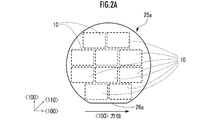
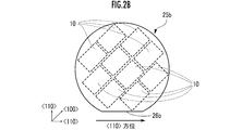
- [SOI wafer] 2A and 2B are front views of the SOI wafers 25a and 25b used for manufacturing the optical deflector 10.
- the front surface of each SOI wafer 25 is the main surface on the front surface side of each SOI wafer 25.
- the coordinate axes shown in FIGS. 2A and 2B indicate the orientation in the active layer 28d (FIG. 11) formed from the silicon single crystal of the SOI wafer 25.
- the orifra 26 indicates the crystal orientation of the active layer 28d (silicon single crystal layer) of the SOI wafer 25.
- a plurality of optical deflectors 10 are cut out from each SOI wafer 25.
- the outer shape of the light deflector 10 is shown by a rectangular wavy line.
- the long side and the short side of the rectangle correspond to the horizontal side (long side) and the vertical side (short side) of the fixed frame portion 16 in the front view of the optical deflector 10 of FIG.
- Orifura 26a is in the direction of ⁇ 100>. Therefore, the surface index of the main surface of the SOI wafer 25a is (100).
- the orientation flat 26b is in the direction of ⁇ 110>. Therefore, the surface index of the main surface of the support layer 28b is (110).
- the substrate layer of the optical deflector 10 is composed of the active layer 28d of the SOI wafer 25.
- the axial direction of the torsion bar 12 is adjusted to ⁇ 100>, the torsional rigidity of the torsion bar 12 becomes high.
- the axial direction of the torsion bar 12 is a direction orthogonal to the orientation flat 26a. Further, in the SOI wafer 25b, the axial direction of the torsion bar 12 is 45 ° with respect to the orientation flat 26b.
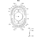
- FIG. 3 is an enlarged view of the range including the torsion bar 12 in FIG.
- the central portion includes a movable frame portion 14, a mirror portion 11 surrounded by the movable frame portion 14 inside, a torsion bar 12, and an inner piezoelectric actuator 13.
- FIG. 3 shows a three-axis coordinate system of X-axis-Y-axis-Z-axis and a direction of crystal orientation.
- the X-axis and the Y-axis correspond to ⁇ 100>.
- the direction of 45 ° with respect to the X-axis and the Y-axis coincides with ⁇ 110>.
- Each torsion bar 12 is connected to the peripheral edge of the mirror portion 11 on the center O side, and is coupled to the movable frame portion 14 on the side opposite to the center O.
- Each inner piezoelectric actuator 13 is coupled to each of the torsion bars 12a and 12b at both ends of the semi-elliptical ring shape, and is coupled to the inner circumference of the movable frame portion 14 at the central portion of the outer circumference of the shape.
- the R portion 31 is formed at the coupling edge portion where each torsion bar 12 is coupled to the mirror portion 11, the inner piezoelectric actuator 13, and the movable frame portion 14 in order to increase the strength.
- the R portion 31 is formed of a curved surface that is dented inward.
- the R portions 31aa and 31ba form a coupling edge portion between each torsion bar 12 and the mirror portion 11.
- the R portions 31ab and 31bb form a coupling edge portion on the mirror portion 11 side of each torsion bar 12 and the inner piezoelectric actuator 13.
- the R portions 31ac and 31bc form a coupling edge portion on the movable frame portion 14 side of each torsion bar 12 and the inner piezoelectric actuator 13.
- the R portions 31ad and 31bd form a coupling edge portion between each torsion bar 12 and the inner peripheral side of the movable frame portion 14.
- the R portion 31 is formed to reinforce the corner portion (corner portion), there is a problem with this optical deflector 10. That is, as described above in FIGS. 2A and 2B, the curved surface of the R portion 31 formed at each connecting edge portion of the torsion bar 12 in order to align the axial direction of the torsion bar 12 with ⁇ 100> of the active layer 28d. Includes a plane whose cleavage direction is ⁇ 110>, in other words, a plane whose normal is in the direction of ⁇ 110>. As a result, cleavage easily proceeds from the portion of the surface element to the curved surface.
- FIG. 4 is an image of the surface stress distribution of the torsion bar 12 by simulation.
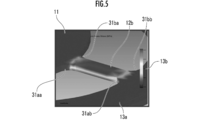
- FIG. 5 is an image of the distribution of cross-sectional stress of the torsion bar 12 by simulation.
- the whitish region means that the stress is higher.
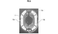
- FIG. 6 is a microscopic observation diagram observing the destruction of the torsion bar 12 in the optical deflector 10 in which the measures against the amount of swell described later in the R section 31 are not taken.
- FIG. 7 is an SEM observation image of the fracture surface 37 of FIG. 6 observed from a predetermined direction.
- the torsion bar 12b is damaged between the mirror portion 11 and the inner piezoelectric actuator 13 due to the destruction of the R portion 31.
- the fracture surface 37 and the surface 35 (front surface) and the curved surface 36 (curved curved surface) in the vicinity thereof are projected.
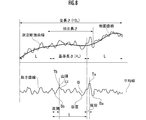
- FIG. 8 is an explanatory diagram of the amount of swell when the JIS standard for surface roughness is applied to the R portion 31.
- the JIS standard is "JIS B 0601-1994", but it shall include standards equivalent thereto.
- the measurement cross-section curve is a contour line when the curved surface of the R portion 31 is cut by a predetermined cross-section parallel to the XY plane (example: a cross-section passing through the center of the thickness of the Z-axis).
- both ends of the contour line are positioned so that the contour of the R portion 31 is parallel to ⁇ 100>.
- the measurement cross-sectional curve is divided into three equal parts in the direction of the reference length (horizontal axis in FIG. 8). Let L be the length of each division in the direction of the reference length.
- the swell curve is defined as the contour line when the R portion 31 is cut by a plane parallel to the main surface of the SOI wafer 25.
- the average line by the least squares method is set for the measurement cross-sectional curve.
- the mean line by the least squares method is set for the swell curve. Then, the distance from the average line at each position on the swell curve is defined as the amount of swell.
- the period means the section between the summits when the roughness curve is replaced with the swell curve in FIG.
- the plane is the surface of the R portion 31.
- the surface of the R portion 31 is located at a shallow position from the surface of the light deflector 10, so that the contour line of the R portion 31 can be easily measured.
- Ta and Ba indicate the maximum swell amount and the minimum swell amount in the cycle in which the difference between the maximum swell amount and the minimum swell amount is the maximum in the entire cycle of the R portion 31.
- Tb and Bb indicate the maximum swell amount and the minimum swell amount in the period in which the difference between the maximum swell amount and the minimum swell amount is the maximum among the cycles included in the central division in the trisection. There is a relationship of the difference of Tb-Bb ⁇ the difference of Ta-Ba.
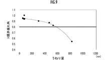
- FIG. 9 is a graph of the relationship between the swell amount of the R portion 31 and the H limit runout angle.
- the "H limit runout angle” is the maximum runout angle of the mirror portion 11 around the rotation axis 22y when the torsion bar 12 is broken.
- the optical deflector 10 In order to prevent the torsion bar 12 from breaking, the optical deflector 10 must be used with the runout angle of the mirror portion 11 around the rotation axis 22y set to less than the H limit runout angle.
- runout angles of the mirror unit 11 There are two types of runout angles of the mirror unit 11: a runout angle around the rotation axis 22y and a runout angle around the rotation axis 22x.
- H runout angle the runout angle around the rotation axis 22y
- V runout angle the runout angle around the rotation axis 22x
- H runout angle and V runout angle are both defined as 0 °.
- each of these runout angles is a mechanical runout angle.
- each numerical value on the vertical axis means a relative value of the H limit swing angle.
- the amount of undulation of the curved surface of the R portion 31 should be set within 600 nm.
- each R portion 31 is formed by a cylindrical curved surface dented inward as a connecting edge between each element.
- the predetermined portion of the R portion 31 is formed so that the unevenness with respect to the curved surface of the cylinder is 600 nm or less.
- Both ends of the predetermined portion are set outside both ends of the central divided portion when the cylindrical curved surface is divided into three equal parts.
- the central divided portion corresponds to the central curved portion of the three curved portions in the reference length direction (horizontal axis direction).
- the cylindrical curved surface includes the ideal side surface of the cylinder (side surface with zero unevenness). Further, with respect to the ideal side surface of the cylinder, the side surface that fits in the unevenness within a predetermined first threshold value, or the amount of ridge or sedimentation per unit length of the side surface that fits in the unevenness within a predetermined first threshold value and is in an arbitrary direction of the side surface. A curved surface within the second threshold is also included.
- the reason for setting both ends of the predetermined part to the outside of both ends of the central divided part is as follows. That is, since the axial direction of the torsion bar 12 is ⁇ 100> of the crystal orientation of the silicon single crystal layer, the cleavage direction in the R portion 31 exists in the central divided portion when the cylindrical curved surface is divided into three equal parts. Because.
- FIG. 10 is a process chart of a method for manufacturing the optical deflector 10 in which the amount of swell of the R portion 31 is within 600 nm, and is an example particularly related to the SOI processing process.
- an SOI wafer 25 (SOI wafer 25a in FIG. 2A or SOI wafer 25b in FIG. 2B) is prepared.
- the element forming layer 42 is formed on the surface 40 of the SOI wafer 25.
- the element forming layer 42 is the electrode layer 42a, the piezoelectric film layer 42b, and the electrode layer 42c in FIG.
- STEP3 corresponds to the coating process.
- the spin rotation 45 is operated while dropping the photosensitizer 44 from the nozzle 43 on the SOI wafer 25 with the surface 40.
- the photosensitizer 44 spreads uniformly on the surface of the element forming layer 42.
- AZ4620 viscosity: 400 cSt
- the spin rotation 45 is 1000 rpm to 2000 rpm.
- the film thickness of the resist film layer formed on the surface of the device forming layer 42 was larger than 10 ⁇ m.
- the rotation speed of the spin rotation 45 is increased to reduce the film thickness of the resist film layer 48, the film thickness unevenness increases this time.
- the photosensitizer 44 (viscosity: 70 cSt).
- the spin rotation 45 is 500 rpm to 1000 rpm.
- the resist film layer 48 having a uniform film thickness is formed on the surface side of the element forming layer 42.
- the film thickness of the resist film layer 48 is 5 ⁇ m or more and 10 ⁇ m or less.
- the film thickness is less than 5 ⁇ m, it will not be possible to cover the stepped structure of the unevenness of the MEMS. Further, if the film thickness exceeds 10 ⁇ m, the photosensitive agent 44 cannot be uniformly applied to the surface of the element forming layer 42, and it becomes unsatisfactory that the amount of undulation of the curved surface of the R portion 31 is within 600 nm. ..
- the photomask 50 is coated on the SOI wafer 25 with the resist film layer 48.
- the photomask 50 has a pattern 52 according to the number and arrangement of the optical deflectors 10 manufactured from one SOI wafer 25.
- ultraviolet light 51 is further irradiated from the surface side of the photomask 50.
- the region of the pattern 52 of the photomask 50 in the resist film layer 48 is exposed by the ultraviolet light 51.
- FIG. 11 is a cross-sectional view of the optical deflector 10 manufactured after STEP 5 and further through an etching process.
- the SOI wafer 25 has a SiO2 layer 28a, a support layer 28b, a SiO2 layer 28c, an active layer 28d, and a SiO2 layer 28e laminated from the back surface side to the front surface side.
- the element forming layer 42 has an electrode layer 42a, a piezoelectric film layer 42b, and an electrode layer 42c laminated in this order from the SOI wafer 25 side.
- the mirror portion 11 has a metal layer 54 that covers the surface of the SiO2 layer 28e.
- the surface of the metal layer 54 serves as a reflection surface for light incident on the mirror portion 11 from a light source (not shown).
- the active layer 28d forms a common substrate layer of the mirror portion 11, the inner piezoelectric actuator 13, and the outer piezoelectric actuator 15.
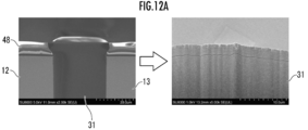
- FIG. 12A is an SEM observation image of observing the cross section of the resist film layer 48 in which the thickness of the resist film layer 48 exceeds the specified 10 ⁇ m and the amount of undulation of the curved curved surface of the R portion 31 manufactured with the thickness.
- FIG. 12B is an SEM observation image of observing the cross section of the resist film layer 48 in which the thickness of the resist film layer 48 is within the specified 10 ⁇ m and the amount of undulation of the curved curved surface of the R portion 31 manufactured with the thickness. ..
- the light deflector 10 of the embodiment is a two-axis type, that is, an optical deflector that scans the scanning light from the mirror portion in two dimensions.
- the optical deflector of the present invention may be a uniaxial type, that is, an optical deflector that scans the scanning light from the mirror portion in one dimension.
- the optical deflector 10 of the embodiment exceeds the coupling portion with the inner piezoelectric actuator 13 as the piezoelectric actuator in the Y-axis direction, reaches the inner circumference of the movable frame portion 14 (movable frame), and is coupled to the inner circumference. doing.
- the torsion bar does not have to be coupled to the movable frame portion 14 as the support portion.
- the photosensitive agent 44 as the resist film layer 48 as the photoresist film uses AZ6130 (viscosity: 70 cSt).
- the photosensitive agent for forming the photoresist film of the present invention is a photosensitive agent as long as the surface side of the substrate before the exposure step can be coated with a photoresist film having a uniform thickness of 5 ⁇ m or more and 10 ⁇ m or less. The type does not matter.
- the R parts 31aa and 31ba of the embodiment correspond to the first R part of the present invention.
- the R parts 31ab and 31bb correspond to the second R part of the present invention.
- the entire surface 40 of the SOI 25 is covered with a resist film layer 48 having a film thickness of 5 ⁇ m or more and 10 ⁇ m or less. Therefore, not only the R portions 31aa, 31ba, 31ab, 31bb, but also the other R portions 31ac, 31bc, 31ad, 31bd, and the amount of swelling of the R portion of the connecting portion of the cantilever 19 connected by the meander pattern. , Within 600 nm. In the present invention, the R portion whose swell amount is within 600 nm may be only the R portions 31ab and 31bb.
- the entire surface 40 of the SOI 25 is covered with a resist film layer 48 having a film thickness of 5 ⁇ m or more and 10 ⁇ m or less. Therefore, the difference between the maximum swell amount and the minimum swell amount of each cycle included in the total length of the roughness curve of the R part is not limited to each period included in the extraction length range of the roughness curve of the R part. Can be 600 nm or less.
Landscapes
- Physics & Mathematics (AREA)
- General Physics & Mathematics (AREA)
- Optics & Photonics (AREA)
- Engineering & Computer Science (AREA)
- Manufacturing & Machinery (AREA)
- Mechanical Optical Scanning Systems (AREA)
- Micromachines (AREA)
- Mechanical Light Control Or Optical Switches (AREA)
Priority Applications (3)
| Application Number | Priority Date | Filing Date | Title |
|---|---|---|---|
| US17/616,605 US12248138B2 (en) | 2019-06-06 | 2020-05-20 | Light deflector and manufacturing method |
| CN202080040745.4A CN113906325B (zh) | 2019-06-06 | 2020-05-20 | 光偏转器及其制造方法 |
| EP20818091.9A EP3982186A4 (en) | 2019-06-06 | 2020-05-20 | LIGHT DEFLECTOR AND METHOD OF MANUFACTURING |
Applications Claiming Priority (2)
| Application Number | Priority Date | Filing Date | Title |
|---|---|---|---|
| JP2019106111A JP7297538B2 (ja) | 2019-06-06 | 2019-06-06 | 光偏向器及び製造方法 |
| JP2019-106111 | 2019-06-06 |
Publications (1)
| Publication Number | Publication Date |
|---|---|
| WO2020246245A1 true WO2020246245A1 (ja) | 2020-12-10 |
Family
ID=73652846
Family Applications (1)
| Application Number | Title | Priority Date | Filing Date |
|---|---|---|---|
| PCT/JP2020/019976 Ceased WO2020246245A1 (ja) | 2019-06-06 | 2020-05-20 | 光偏向器及び製造方法 |
Country Status (5)
| Country | Link |
|---|---|
| US (1) | US12248138B2 (enExample) |
| EP (1) | EP3982186A4 (enExample) |
| JP (1) | JP7297538B2 (enExample) |
| CN (1) | CN113906325B (enExample) |
| WO (1) | WO2020246245A1 (enExample) |
Cited By (1)
| Publication number | Priority date | Publication date | Assignee | Title |
|---|---|---|---|---|
| EP4089048A1 (en) * | 2021-05-14 | 2022-11-16 | Stanley Electric Co., Ltd. | Light deflector |
Families Citing this family (2)
| Publication number | Priority date | Publication date | Assignee | Title |
|---|---|---|---|---|
| JP2023008577A (ja) * | 2021-07-06 | 2023-01-19 | スタンレー電気株式会社 | 光偏向器 |
| JP7751997B2 (ja) * | 2021-07-13 | 2025-10-09 | スタンレー電気株式会社 | Mems光偏向器及び光走査装置 |
Citations (6)
| Publication number | Priority date | Publication date | Assignee | Title |
|---|---|---|---|---|
| JP2006319387A (ja) * | 2005-05-10 | 2006-11-24 | Seiko Epson Corp | Memsレゾネータ |
| US20070008401A1 (en) * | 2005-07-07 | 2007-01-11 | Lexmark International, Inc. | Multiharmonic galvanometric scanning device |
| WO2010131557A1 (ja) * | 2009-05-11 | 2010-11-18 | ミツミ電機株式会社 | アクチュエータ及びアクチュエータを用いた光走査装置 |
| JP2012063413A (ja) * | 2010-09-14 | 2012-03-29 | Ricoh Co Ltd | 光走査装置およびこの光走査装置を組み込んだ画像形成装置ならびに投影装置 |
| JP2014102354A (ja) * | 2012-11-19 | 2014-06-05 | Stanley Electric Co Ltd | 光偏向器 |
| JP2017151476A (ja) | 2017-05-24 | 2017-08-31 | ミツミ電機株式会社 | 光走査装置 |
Family Cites Families (8)
| Publication number | Priority date | Publication date | Assignee | Title |
|---|---|---|---|---|
| US6613591B1 (en) * | 2002-03-07 | 2003-09-02 | Memc Electronic Materials, Inc. | Method of estimating post-polishing waviness characteristics of a semiconductor wafer |
| US6872319B2 (en) * | 2002-09-30 | 2005-03-29 | Rockwell Scientific Licensing, Llc | Process for high yield fabrication of MEMS devices |
| WO2005083493A1 (ja) * | 2004-02-27 | 2005-09-09 | Matsushita Electric Industrial Co., Ltd. | 照明光源及びそれを用いた2次元画像表示装置 |
| JP2009031643A (ja) * | 2007-07-30 | 2009-02-12 | Canon Inc | 揺動体装置、光偏向器およびそれを用いた画像形成装置 |
| JP5172364B2 (ja) * | 2008-01-16 | 2013-03-27 | スタンレー電気株式会社 | 光偏向器 |
| JP5397136B2 (ja) * | 2009-09-30 | 2014-01-22 | 住友電気工業株式会社 | Iii族窒化物半導体レーザ素子、及びiii族窒化物半導体レーザ素子を作製する方法 |
| JP6369742B2 (ja) * | 2014-02-26 | 2018-08-08 | 北陽電機株式会社 | 微小機械装置 |
| JP6809018B2 (ja) * | 2016-07-26 | 2021-01-06 | 株式会社リコー | 光偏向器、光走査装置、画像形成装置及び画像投影装置 |
-
2019
- 2019-06-06 JP JP2019106111A patent/JP7297538B2/ja active Active
-
2020
- 2020-05-20 WO PCT/JP2020/019976 patent/WO2020246245A1/ja not_active Ceased
- 2020-05-20 CN CN202080040745.4A patent/CN113906325B/zh active Active
- 2020-05-20 US US17/616,605 patent/US12248138B2/en active Active
- 2020-05-20 EP EP20818091.9A patent/EP3982186A4/en active Pending
Patent Citations (6)
| Publication number | Priority date | Publication date | Assignee | Title |
|---|---|---|---|---|
| JP2006319387A (ja) * | 2005-05-10 | 2006-11-24 | Seiko Epson Corp | Memsレゾネータ |
| US20070008401A1 (en) * | 2005-07-07 | 2007-01-11 | Lexmark International, Inc. | Multiharmonic galvanometric scanning device |
| WO2010131557A1 (ja) * | 2009-05-11 | 2010-11-18 | ミツミ電機株式会社 | アクチュエータ及びアクチュエータを用いた光走査装置 |
| JP2012063413A (ja) * | 2010-09-14 | 2012-03-29 | Ricoh Co Ltd | 光走査装置およびこの光走査装置を組み込んだ画像形成装置ならびに投影装置 |
| JP2014102354A (ja) * | 2012-11-19 | 2014-06-05 | Stanley Electric Co Ltd | 光偏向器 |
| JP2017151476A (ja) | 2017-05-24 | 2017-08-31 | ミツミ電機株式会社 | 光走査装置 |
Non-Patent Citations (1)
| Title |
|---|
| See also references of EP3982186A4 |
Cited By (5)
| Publication number | Priority date | Publication date | Assignee | Title |
|---|---|---|---|---|
| EP4089048A1 (en) * | 2021-05-14 | 2022-11-16 | Stanley Electric Co., Ltd. | Light deflector |
| US20220365338A1 (en) * | 2021-05-14 | 2022-11-17 | Stanley Electric Co., Ltd. | Light deflector |
| JP2022175658A (ja) * | 2021-05-14 | 2022-11-25 | スタンレー電気株式会社 | 光偏向器 |
| JP7600030B2 (ja) | 2021-05-14 | 2024-12-16 | スタンレー電気株式会社 | 光偏向器 |
| US12332427B2 (en) * | 2021-05-14 | 2025-06-17 | Stanley Electric Co., Ltd. | Light deflector |
Also Published As
| Publication number | Publication date |
|---|---|
| US20220236556A1 (en) | 2022-07-28 |
| US12248138B2 (en) | 2025-03-11 |
| CN113906325A (zh) | 2022-01-07 |
| JP2020201308A (ja) | 2020-12-17 |
| CN113906325B (zh) | 2024-12-10 |
| JP7297538B2 (ja) | 2023-06-26 |
| EP3982186A1 (en) | 2022-04-13 |
| EP3982186A4 (en) | 2023-06-21 |
Similar Documents
| Publication | Publication Date | Title |
|---|---|---|
| WO2020246245A1 (ja) | 光偏向器及び製造方法 | |
| KR101191203B1 (ko) | 스캐닝 마이크로미러 | |
| US6924914B2 (en) | Light deflector, method of manufacturing light deflector, optical device using light deflector, and torsion oscillating member | |
| JP6803483B2 (ja) | 光学系における倍率補正及び/又はビームステアリング | |
| US11360393B2 (en) | Mirror, in particular for a microlithographic projection exposure system | |
| US8279509B2 (en) | MEMS-scanning mirror device and method for manufacturing the same | |
| US20110170157A1 (en) | Moving structure and micro-mirror device using the same | |
| JP6966954B2 (ja) | 光偏向器 | |
| CN110275287B (zh) | 光扫描装置 | |
| JPH10142543A (ja) | 光走査装置 | |
| JP3620767B2 (ja) | 反射型走査光学系 | |
| US8079893B2 (en) | Method of remedying glass substrate defect | |
| CN114026484B (zh) | 光偏转器的制造方法及光偏转器 | |
| CN117651912A (zh) | 可变形反射镜系统 | |
| JP2020201308A5 (enExample) | ||
| CN120077314A (zh) | 光偏转器 | |
| JP2021163937A (ja) | Mems圧電アクチュエータ製造方法 | |
| JP2001147393A (ja) | 走査光学系 | |
| US11885957B2 (en) | Optical deflector | |
| WO2024116520A1 (ja) | 光学反射素子 | |
| CN120604160A (zh) | 驱动元件和光偏转元件 | |
| TWI250781B (en) | f-theta lens of laser scanning unit and manufacturing method thereof | |
| WO2025154412A1 (ja) | ミラー装置の製造方法、及びミラー装置 | |
| CN117805773A (zh) | Mems振镜、振镜结构、振镜调节装置及激光雷达系统 | |
| JP2001147391A (ja) | 走査光学系 |
Legal Events
| Date | Code | Title | Description |
|---|---|---|---|
| 121 | Ep: the epo has been informed by wipo that ep was designated in this application |
Ref document number: 20818091 Country of ref document: EP Kind code of ref document: A1 |
|
| NENP | Non-entry into the national phase |
Ref country code: DE |
|
| WWE | Wipo information: entry into national phase |
Ref document number: 2020818091 Country of ref document: EP |
|
| WWG | Wipo information: grant in national office |
Ref document number: 17616605 Country of ref document: US |