WO2020218442A1 - 電力変換装置の制御装置 - Google Patents
電力変換装置の制御装置 Download PDFInfo
- Publication number
- WO2020218442A1 WO2020218442A1 PCT/JP2020/017548 JP2020017548W WO2020218442A1 WO 2020218442 A1 WO2020218442 A1 WO 2020218442A1 JP 2020017548 W JP2020017548 W JP 2020017548W WO 2020218442 A1 WO2020218442 A1 WO 2020218442A1
- Authority
- WO
- WIPO (PCT)
- Prior art keywords
- voltage
- determination value
- value
- determination
- unit
- Prior art date
- Legal status (The legal status is an assumption and is not a legal conclusion. Google has not performed a legal analysis and makes no representation as to the accuracy of the status listed.)
- Ceased
Links
Images


Classifications
-
- H—ELECTRICITY
- H02—GENERATION; CONVERSION OR DISTRIBUTION OF ELECTRIC POWER
- H02M—APPARATUS FOR CONVERSION BETWEEN AC AND AC, BETWEEN AC AND DC, OR BETWEEN DC AND DC, AND FOR USE WITH MAINS OR SIMILAR POWER SUPPLY SYSTEMS; CONVERSION OF DC OR AC INPUT POWER INTO SURGE OUTPUT POWER; CONTROL OR REGULATION THEREOF
- H02M1/00—Details of apparatus for conversion
- H02M1/0003—Details of control, feedback or regulation circuits
-
- H—ELECTRICITY
- H02—GENERATION; CONVERSION OR DISTRIBUTION OF ELECTRIC POWER
- H02M—APPARATUS FOR CONVERSION BETWEEN AC AND AC, BETWEEN AC AND DC, OR BETWEEN DC AND DC, AND FOR USE WITH MAINS OR SIMILAR POWER SUPPLY SYSTEMS; CONVERSION OF DC OR AC INPUT POWER INTO SURGE OUTPUT POWER; CONTROL OR REGULATION THEREOF
- H02M7/00—Conversion of AC power input into DC power output; Conversion of DC power input into AC power output
- H02M7/02—Conversion of AC power input into DC power output without possibility of reversal
- H02M7/04—Conversion of AC power input into DC power output without possibility of reversal by static converters
- H02M7/12—Conversion of AC power input into DC power output without possibility of reversal by static converters using discharge tubes with control electrode or semiconductor devices with control electrode
- H02M7/21—Conversion of AC power input into DC power output without possibility of reversal by static converters using discharge tubes with control electrode or semiconductor devices with control electrode using devices of a triode or transistor type requiring continuous application of a control signal
- H02M7/217—Conversion of AC power input into DC power output without possibility of reversal by static converters using discharge tubes with control electrode or semiconductor devices with control electrode using devices of a triode or transistor type requiring continuous application of a control signal using semiconductor devices only
- H02M7/219—Conversion of AC power input into DC power output without possibility of reversal by static converters using discharge tubes with control electrode or semiconductor devices with control electrode using devices of a triode or transistor type requiring continuous application of a control signal using semiconductor devices only in a bridge configuration
-
- H—ELECTRICITY
- H02—GENERATION; CONVERSION OR DISTRIBUTION OF ELECTRIC POWER
- H02M—APPARATUS FOR CONVERSION BETWEEN AC AND AC, BETWEEN AC AND DC, OR BETWEEN DC AND DC, AND FOR USE WITH MAINS OR SIMILAR POWER SUPPLY SYSTEMS; CONVERSION OF DC OR AC INPUT POWER INTO SURGE OUTPUT POWER; CONTROL OR REGULATION THEREOF
- H02M1/00—Details of apparatus for conversion
- H02M1/0067—Converter structures employing plural converter units, other than for parallel operation of the units on a single load
- H02M1/007—Plural converter units in cascade
-
- H—ELECTRICITY
- H02—GENERATION; CONVERSION OR DISTRIBUTION OF ELECTRIC POWER
- H02M—APPARATUS FOR CONVERSION BETWEEN AC AND AC, BETWEEN AC AND DC, OR BETWEEN DC AND DC, AND FOR USE WITH MAINS OR SIMILAR POWER SUPPLY SYSTEMS; CONVERSION OF DC OR AC INPUT POWER INTO SURGE OUTPUT POWER; CONTROL OR REGULATION THEREOF
- H02M1/00—Details of apparatus for conversion
- H02M1/08—Circuits specially adapted for the generation of control voltages for semiconductor devices incorporated in static converters
- H02M1/083—Circuits specially adapted for the generation of control voltages for semiconductor devices incorporated in static converters for the ignition at the zero crossing of the voltage or the current
-
- H—ELECTRICITY
- H02—GENERATION; CONVERSION OR DISTRIBUTION OF ELECTRIC POWER
- H02M—APPARATUS FOR CONVERSION BETWEEN AC AND AC, BETWEEN AC AND DC, OR BETWEEN DC AND DC, AND FOR USE WITH MAINS OR SIMILAR POWER SUPPLY SYSTEMS; CONVERSION OF DC OR AC INPUT POWER INTO SURGE OUTPUT POWER; CONTROL OR REGULATION THEREOF
- H02M1/00—Details of apparatus for conversion
- H02M1/32—Means for protecting converters other than automatic disconnection
-
- H—ELECTRICITY
- H02—GENERATION; CONVERSION OR DISTRIBUTION OF ELECTRIC POWER
- H02M—APPARATUS FOR CONVERSION BETWEEN AC AND AC, BETWEEN AC AND DC, OR BETWEEN DC AND DC, AND FOR USE WITH MAINS OR SIMILAR POWER SUPPLY SYSTEMS; CONVERSION OF DC OR AC INPUT POWER INTO SURGE OUTPUT POWER; CONTROL OR REGULATION THEREOF
- H02M1/00—Details of apparatus for conversion
- H02M1/42—Circuits or arrangements for compensating for or adjusting power factor in converters or inverters
- H02M1/4208—Arrangements for improving power factor of AC input
- H02M1/4233—Arrangements for improving power factor of AC input using a bridge converter comprising active switches
-
- H—ELECTRICITY
- H02—GENERATION; CONVERSION OR DISTRIBUTION OF ELECTRIC POWER
- H02M—APPARATUS FOR CONVERSION BETWEEN AC AND AC, BETWEEN AC AND DC, OR BETWEEN DC AND DC, AND FOR USE WITH MAINS OR SIMILAR POWER SUPPLY SYSTEMS; CONVERSION OF DC OR AC INPUT POWER INTO SURGE OUTPUT POWER; CONTROL OR REGULATION THEREOF
- H02M3/00—Conversion of DC power input into DC power output
- H02M3/02—Conversion of DC power input into DC power output without intermediate conversion into AC
- H02M3/04—Conversion of DC power input into DC power output without intermediate conversion into AC by static converters
- H02M3/10—Conversion of DC power input into DC power output without intermediate conversion into AC by static converters using discharge tubes with control electrode or semiconductor devices with control electrode
- H02M3/145—Conversion of DC power input into DC power output without intermediate conversion into AC by static converters using discharge tubes with control electrode or semiconductor devices with control electrode using devices of a triode or transistor type requiring continuous application of a control signal
- H02M3/155—Conversion of DC power input into DC power output without intermediate conversion into AC by static converters using discharge tubes with control electrode or semiconductor devices with control electrode using devices of a triode or transistor type requiring continuous application of a control signal using semiconductor devices only
- H02M3/156—Conversion of DC power input into DC power output without intermediate conversion into AC by static converters using discharge tubes with control electrode or semiconductor devices with control electrode using devices of a triode or transistor type requiring continuous application of a control signal using semiconductor devices only with automatic control of output voltage or current, e.g. switching regulators
- H02M3/158—Conversion of DC power input into DC power output without intermediate conversion into AC by static converters using discharge tubes with control electrode or semiconductor devices with control electrode using devices of a triode or transistor type requiring continuous application of a control signal using semiconductor devices only with automatic control of output voltage or current, e.g. switching regulators including plural semiconductor devices as final control devices for a single load
-
- H—ELECTRICITY
- H02—GENERATION; CONVERSION OR DISTRIBUTION OF ELECTRIC POWER
- H02M—APPARATUS FOR CONVERSION BETWEEN AC AND AC, BETWEEN AC AND DC, OR BETWEEN DC AND DC, AND FOR USE WITH MAINS OR SIMILAR POWER SUPPLY SYSTEMS; CONVERSION OF DC OR AC INPUT POWER INTO SURGE OUTPUT POWER; CONTROL OR REGULATION THEREOF
- H02M7/00—Conversion of AC power input into DC power output; Conversion of DC power input into AC power output
- H02M7/02—Conversion of AC power input into DC power output without possibility of reversal
- H02M7/04—Conversion of AC power input into DC power output without possibility of reversal by static converters
- H02M7/12—Conversion of AC power input into DC power output without possibility of reversal by static converters using discharge tubes with control electrode or semiconductor devices with control electrode
- H02M7/145—Conversion of AC power input into DC power output without possibility of reversal by static converters using discharge tubes with control electrode or semiconductor devices with control electrode using devices of a thyratron or thyristor type requiring extinguishing means
- H02M7/155—Conversion of AC power input into DC power output without possibility of reversal by static converters using discharge tubes with control electrode or semiconductor devices with control electrode using devices of a thyratron or thyristor type requiring extinguishing means using semiconductor devices only
- H02M7/162—Conversion of AC power input into DC power output without possibility of reversal by static converters using discharge tubes with control electrode or semiconductor devices with control electrode using devices of a thyratron or thyristor type requiring extinguishing means using semiconductor devices only in a bridge configuration
- H02M7/1623—Conversion of AC power input into DC power output without possibility of reversal by static converters using discharge tubes with control electrode or semiconductor devices with control electrode using devices of a thyratron or thyristor type requiring extinguishing means using semiconductor devices only in a bridge configuration with control circuit
- H02M7/1626—Conversion of AC power input into DC power output without possibility of reversal by static converters using discharge tubes with control electrode or semiconductor devices with control electrode using devices of a thyratron or thyristor type requiring extinguishing means using semiconductor devices only in a bridge configuration with control circuit with automatic control of the output voltage or current
Definitions
- the present disclosure relates to a control device for a power conversion device.
- Patent Document 1 discloses a control device that operates a drive switch by well-known peak current mode control in order to control the reactor current flowing through the reactor of the AC / DC conversion device to a current command value.
- This control device acquires the voltage of the AC power supply as a detection voltage, and adds a current correction value that changes according to the phase of the acquired detection voltage to the current command value to reduce distortion of the output current.
- the timing at which the polarity of the actual voltage, which is the actual voltage of the AC power supply, changes based on the detection voltage detected by the voltage sensor is determined, and the switches that make up the full bridge circuit are synchronized with this timing.
- the polarity of the actual voltage is switched at the switching timing between the set of switches to be turned on and the set of switches to be turned off due to a phase shift or vertical offset in the detected voltage with respect to the actual voltage. It may deviate from the timing.
- the present disclosure has been made in view of the above problems, and an object of the present disclosure is to provide a control device of a power conversion device capable of suppressing an overcurrent from flowing in a control device of a power conversion device including a full bridge circuit.
- the present disclosure describes the reactor, the first AC side terminal, the second AC side terminal, the first DC side terminal, the second DC side terminal, and between each AC side terminal and the reactor.
- the present invention relates to a control device for a power conversion device having at least one of the functions of converting a DC voltage input from a side terminal into an AC voltage and outputting the DC voltage from each of the AC side terminals.
- the full bridge circuit has a series connection body of a first switch and a second switch, and a series connection body of a third switch and a fourth switch, and each series connection body is connected in parallel.
- a diode is connected in antiparallel to each of the first switch, the second switch, the third switch, and the fourth switch, and the first switch and the second switch are connected to the first AC side terminal.
- the connection point between the third switch and the fourth switch is connected to the second AC side terminal.
- the control device actually performs the AC power supply by comparing the detected voltage acquisition unit that acquires the detection voltage which is the voltage value of the AC power supply detected by the voltage sensor with the voltage determination value.
- the first switch and the fourth switch It is provided with an operation unit that alternately switches the set to be turned on among the set and the set of the second switch and the third switch.
- the voltage determination value is a first determination value for determining the timing at which the actual voltage crosses zero up and a second determination value for determining the timing at which the actual voltage crosses zero down, and has the polarity.
- the determination unit determines that the period from when the acquired detection voltage exceeds the first determination value to when it falls below the second determination value is a period during which the actual voltage is positive, and the acquired detection. The period from when the voltage falls below the second determination value to when it exceeds the first determination value is determined to be the period during which the actual voltage is negative.
- the detected voltage of the voltage sensor deviates from the actual voltage at the timing when the actual voltage crosses zero.
- the polarity of the actual voltage is determined by comparing the detection voltage with the first determination value for determining the timing at which the actual voltage crosses zero up and the second determination value for determining the timing for zero downcross. To. Specifically, the period from when the detected voltage exceeds the first judgment value to when it falls below the second judgment value is determined to be the period during which the actual voltage is positive, and the detection voltage falls below the second judgment value. The period from to exceeding the first determination value is determined to be the period during which the actual voltage is negative.
- the set of the first and fourth switches and the set of the second and third switches that are turned on can be operated. It is suppressed that the operation timing deviates from the timing at which the polarity of the actual voltage is switched. As a result, it is possible to prevent an overcurrent from flowing through the power converter.
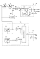
- FIG. 1 is a configuration diagram of a power conversion device.
- FIG. 2 is a circuit diagram of the AC voltage sensor.
- FIG. 3 is a functional block diagram of the control device.
- FIG. 4 is a configuration diagram of the current correction unit.
- FIG. 5 is a timing chart illustrating the operation of the power converter.
- FIG. 6 is a diagram for explaining the details of the overcurrent flowing through the first and second AC side terminals T.
- FIG. 7 is a diagram for explaining the details of the overcurrent flowing through the first and second AC side terminals.
- FIG. 8 is a diagram for explaining the first and second determination values.
- FIG. 1 is a configuration diagram of a power conversion device.
- FIG. 2 is a circuit diagram of the AC voltage sensor.
- FIG. 3 is a functional block diagram of the control device.
- FIG. 4 is a configuration diagram of the current correction unit.
- FIG. 5 is a timing chart illustrating the operation of the power converter.
- FIG. 6 is a diagram for explaining the details
- FIG. 9 is a diagram illustrating the operation and effect of the present embodiment.
- FIG. 10 is a diagram for explaining the action and effect of the comparative example.
- FIG. 11 is a diagram illustrating a method of creating a reference correction value map.
- FIG. 12 is a functional block diagram of the control device according to the second embodiment.
- FIG. 13 is a diagram for explaining how the detection voltage corresponding to the zero cross timing of the actual voltage changes as the amplitude changes.
- FIG. 14 is a diagram illustrating how the detected voltage changes with voltage fluctuations.
- FIG. 15 is a diagram for explaining how the detected voltage changes with the voltage fluctuation.
- FIG. 16 is a diagram for explaining a determination signal according to a modified example of the second embodiment.
- FIG. 17 is a functional block diagram of the control device according to the third embodiment.
- FIG. 18 is a functional block diagram of the control device according to the fourth embodiment.
- FIG. 19 is a diagram illustrating a connection state between the power conversion device and the AC power supply according to the fifth embodiment.
- FIG. 20 is a functional block diagram of the control device.
- FIG. 21 is a diagram illustrating a polarity determination unit according to a modified example of the fifth embodiment.
- the power conversion device converts the DC power supplied from the DC power supply through the DC side terminal into AC power and supplies it to the AC power supply.
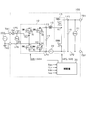
- DC power supplies (not shown) are connected to the first and second DC side terminals TD1 and TD2 of the power conversion device 100 shown in FIG. 1, and AC power supplies are connected to the first and second AC side terminals TA1 and TA2. 200 is connected.
- the AC power supply 200 is, for example, a commercial power supply, and the DC power supply is, for example, a battery or a DC / DC conversion circuit.
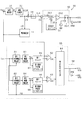
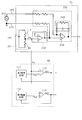
- the power conversion device 100 includes a capacitor 16, a half-bridge circuit 15, an intermediate capacitor 14, a reactor 13, a full-bridge circuit 12, and first to sixth wirings LP1 to LP6.
- the first end of the first wiring LP1 is connected to the first DC side terminal TD1, and the first end of the second wiring LP2 is connected to the second DC side terminal TD2.
- the first wiring LP1 and the second wiring LP2 are connected by a capacitor 16.
- a half bridge circuit 15 is connected to the second end of the first and second wirings LP1 and LP2.
- the half-bridge circuit 15 includes a fifth switch SW5 and a sixth switch SW6.
- the fifth and sixth switches SW5 and SW6 are voltage-driven switches, and in this embodiment, they are N-channel MOSFETs.
- the source of the fifth switch SW5 and the drain of the sixth switch SW6 are connected.
- the drain of the fifth switch SW5 is connected to the first wiring LP1, and the source of the sixth switch SW6 is connected to the second wiring LP2.
- the half-bridge circuit 15 and the full-bridge circuit 12 are connected by the third wiring LP3 and the fourth wiring LP4.
- the first end of the third wiring LP3 is connected to the first connection point K1 between the source of the fifth switch SW5 and the drain of the sixth switch SW6.
- a reactor 13 is provided on the third wiring LP3.
- the first end of the fourth wiring LP4 is connected to the source of the sixth switch SW6.
- the second ends of the third and fourth wirings LP3 and LP4 are connected to the full bridge circuit 12.
- the third wiring LP3 and the fourth wiring LP4 are connected by an intermediate capacitor 14.
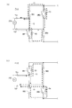
- the full bridge circuit 12 includes first to fourth switches SW1 to SW4.
- the first to fourth switches SW1 to SW4 are voltage-driven switches, and in the present embodiment, they are N-channel MOSFETs.
- the source of the first switch SW1 and the drain of the second switch SW2 are connected.
- the source of the third switch SW3 and the drain of the fourth switch SW4 are connected.
- the drains of the first and third switches SW1 and SW3 are connected to the third wiring LP3, and the sources of the second and fourth switches SW2 and SW4 are connected to the fourth wiring LP4.
- Each of the first to fourth switches SW1 to SW4 includes first to fourth body diodes D1 to D4 connected in antiparallel.
- the second connection point K2 between the source of the third switch SW3 and the drain of the fourth switch SW4 is connected to the first end of the sixth wiring LP6, and the second end of the sixth wiring LP6 is the second alternating current. It is connected to the side terminal TA2.
- the third connection point K3 between the first switch SW1 and the second switch SW2 is connected to the first end of the fifth wiring LP5, and the second end of the fifth wiring LP5 is connected to the first AC side terminal TA1. ing.
- the power conversion device 100 includes a DC voltage sensor 21, a reactor current sensor 22, and an AC voltage sensor 23.
- the DC voltage sensor 21 is connected between the first and second wirings LP1 and LP2, and detects the voltage input through the first and second DC side terminals TD1 and TD2 as the DC voltage Vdc.
- the reactor current sensor 22 is provided in the fourth wiring LP4, and detects the current flowing through the reactor 13 as the reactor current ILr.
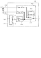
- the AC voltage sensor 23 is connected between the fifth and sixth wirings LP5 and LP6, and detects the voltage of the AC power supply 200 as the detection voltage Vac.
- the AC voltage sensor 23 includes a reference voltage generation unit 231, a voltage follower unit 232, and a differential amplification unit 233.
- the reference voltage generation unit 231 includes a series connection of resistors R1 and R2 and a low voltage source 241.
- the reference voltage Vs is generated by dividing the voltage supplied from the low voltage source 241 by the resistors R1 and R2. Output.
- the reference voltage Vs is a voltage that serves as a reference for the detection voltage Vac of the AC voltage sensor 23, and specifically, is a detection voltage Vac when the actual voltage Vr, which is the actual voltage value of the AC power supply 200, becomes 0. ..
- An AC power supply 200 is connected to the inverting input terminal of the operational amplifier 242 of the differential amplification unit 233 via the fifth wiring LP5, and an AC power supply 200 is connected to the non-inverting input terminal via the sixth wiring LP6. It is connected.
- the inverting input terminal and the output terminal of the operational amplifier 242 are connected by a low-pass filter 243.
- the reference voltage Vs from the reference voltage generation unit 231 is input to the non-inverting input terminal of the operational amplifier 242 via the voltage follower unit 232.
- the operational amplifier 242 outputs a detection voltage Vac corresponding to the actual voltage Vr of the AC power supply 200 centering on the reference voltage Vs.
- the polarity of the detection voltage Vac is defined as follows. When the voltage of the first AC side terminal TA1 is larger than the voltage of the second AC side terminal TA2, it is assumed that the detection voltage Vac is positive, and the voltage of the second AC side terminal TA2 is the voltage of the first AC side terminal TA1. It is assumed that the detection voltage Vac has a negative electrode property in a state larger than the above.
- the power conversion device 100 includes an output current sensor 24 that detects the current flowing through the first and second AC side terminals TA1 and TA2 as the output current Iac.
- the output current sensor 24 is provided on the fifth wiring LP5.
- the output current Iac flowing from the first AC side terminal TA1 to the second AC side terminal TA2 via the AC power supply 200 is positive, and the first AC side terminal TA1 from the second AC side terminal TA2 via the AC power supply 200.
- the output current Iac flowing in the direction of is the negative electrode.
- the detected values of the sensors 21 to 24 are input to the control device 30.
- the control device 30 operates the first to sixth switches SW1 to SW6 on and off.
- Each function provided by the control device 30 can be provided by, for example, software recorded in a substantive memory device, a computer for executing the software, hardware, or a combination thereof.
- the control device 30 turns on / off the fifth and sixth switches SW5 and SW6 by peak current mode control in order to control the acquired reactor current ILr to the command current ILa * calculated based on the detected voltage Vac.
- the control device 30 is the first and fourth switches of the set of the first and fourth switches SW1 and SW4 and the set of the second and third switches SW2 and SW3 during the period when the actual voltage Vr becomes positive.
- the set of SW1 and SW4 is turned on, and the set of the second and third switches SW2 and SW3 is turned on during the period when the actual voltage Vr becomes negative.
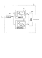
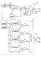
- the control device 30 includes a phase estimation unit 31, a waveform generation unit 32, a multiplier 33, an absolute value calculation unit 34, an adder 35, a current correction unit 40, and a current control unit 50.
- the control device 30 corresponds to the detection voltage acquisition unit.
- the waveform generation unit 32 generates a reference waveform sin ⁇ of the detection voltage Vac based on the phase ⁇ of the detection voltage Vac estimated by the phase estimation unit 31.
- the reference waveform sin ⁇ is a value indicating a voltage change in a half cycle (T / 2) of the detected voltage Vac, has an amplitude of 1, and fluctuates in the same cycle as the detected voltage Vac.
- the reference waveform sin ⁇ has the same phase as the detection voltage Vac.
- the multiplier 33 multiplies the amplitude command value Ia * of the reactor current ILr by the reference waveform sin ⁇ .
- the amplitude command value Ia * is a command value that determines the amplitude of the reactor current ILr.
- the absolute value calculation unit 34 sets the absolute value of the output value from the multiplier 33 as the pre-correction command current IL *.
- the current correction unit 40 sets the current correction value Ic used for correction with respect to the pre-correction command current IL * in order to suppress distortion of the output current Iac.
- the configuration of the current correction unit 40 according to the present embodiment will be described with reference to FIG.
- the deviation width ⁇ i which indicates the difference between the pre-correction command current IL * and the average value Iave of the distorted reactor current ILr, is the smallest value near the actual voltage Vr zero cross timing. It becomes.
- the deviation width ⁇ i causes distortion of the output current Iac.
- the deviation width ⁇ i can be calculated by using the following equation (1) obtained by subtracting the average value Iave of the reactor current ILr from the pre-correction command current IL *. The method for deriving the following equation (1) will be described later.
- the deviation width ⁇ i takes the minimum value at the zero cross timing of the actual voltage Vr and the maximum value at the peak timing of the actual voltage Vr. Therefore, the distortion of the output current Iac can be suppressed by calculating the current correction value Ic according to the deviation width ⁇ i calculated by the above equation (1).
- the current correction unit 40 includes an effective value calculation unit 41, an upper limit value setting unit 42, a reference correction value calculation unit 43, and a minimum value selection unit 44.
- the effective value calculation unit 41 calculates the effective value Vrms of the actual voltage Vr.
- the upper limit value setting unit 42 sets the upper limit value Idc based on the effective value Vrms and the amplitude command value Ia *.
- the upper limit value setting unit 42 includes a DC component map showing the relationship between the amplitude command value Ia * and the upper limit value Idc for each effective value Vrms.
- each effective value Vrms corresponds to the effective value Vrms of the commercial power source of each country. Therefore, the upper limit value setting unit 42 can set the upper limit value Idc according to the amplitude command value Ia * by referring to the DC component map for each effective value Vrms.
- the reference correction value calculation unit 43 sets the reference correction value Ih based on the effective value Vrms.
- the reference correction value Ih set by the reference correction value calculation unit 43 takes a minimum value at or near the zero cross timing of the actual voltage Vr, and takes a maximum value at the peak timing. Specifically, the reference correction value Ih changes with the passage of time. Further, in the present embodiment, the reference correction value Ih is set to zero at the zero cross timing of the actual voltage Vr, but is not limited to this, and is set to a value larger than zero at the zero cross timing of the actual voltage Vr. May be good.
- the reference correction value calculation unit 43 includes a correction value map in which the reference correction value Ih is recorded for each effective value Vrms. The value of each correction value map is determined so that the larger the effective value Vrms, the larger the reference correction value Ih.
- the minimum value selection unit 44 sets the smaller value of the upper limit value Idc set by the upper limit value setting unit 42 and the reference correction value Ih set by the reference correction value calculation unit 43 as the current correction value Ic. To do. Therefore, if the reference correction value Ih is smaller than the upper limit value Idc, the reference correction value Ih is set as the current correction value Ic, and if the reference correction value Ih is a value equal to or higher than the upper limit value Idc, the upper limit value Idc is the current. It is set as the correction value Ic.
- the adder 35 adds the current correction value Ic to the pre-correction command current IL *, and sets the value after the addition as the command current ILa *.
- the command current ILa * corresponds to the current command value.
- the current control unit 50 outputs a fifth gate signal GS5 for operating the fifth switch SW5 and a sixth gate signal GS6 for operating the sixth switch SW6 based on the reactor current ILr and the command current ILa *. ..
- the current control unit 50 includes a DA converter 351, a comparator 352, an adder 353, an RS flip-flop 357, and a slope compensation unit 51.
- the command current ILa * is input to the DA converter 351.
- the DA converter 351 converts the input command current ILa * from a digital value to an analog value.
- the command current ILa * converted into an analog value is input to the inverting input terminal of the comparator 352.
- the adder 353 adds the reactor current ILr and the slope compensation signal Slope set by the slope compensation unit 51, and outputs the compensated reactor current ILr.
- the output from the adder 353 is input to the non-inverting input terminal of the comparator 352.
- the slope compensation signal Slope suppresses oscillation due to fluctuations in the current flowing through the reactor 13.
- the comparator 352 compares the command current ILa * with the reactor current ILr, and inputs a low state signal to the R terminal of the RS flip-flop 357 during a period in which the reactor current ILr is smaller than the command current ILa *. Further, the comparator 352 inputs a high state signal to the R terminal of the RS flip-flop 357 during a period in which the reactor current ILr is larger than the command current ILa *. Further, a clock signal is input to the S terminal of the RS flip-flop 357. One cycle of the clock signal is one switching cycle Tsw of the fifth and sixth switches SW5 and SW6.
- the Q terminal of the RS flip-flop 357 is connected to the gate of the fifth switch SW5.
- the signal output from the Q terminal to the gate of the 5th switch SW5 becomes the 5th gate signal GS5.
- the output terminal of the RS flip-flop 357 is connected to the gate of the sixth switch SW6 via the reversing device 358.
- the signal output from the Q terminal to the gate of the sixth switch SW6 via the reversing device 358 becomes the sixth gate signal GS6.
- the sixth gate signal GS6 is a value obtained by inverting the logic of the fifth gate signal GS5.
- the control device 30 includes a polarity determination unit 55 that determines the polarity of the actual voltage Vr based on the detection voltage Vac.
- the polarity determination unit 55 outputs the polarity determination signal PS in the high state during the period for determining that the polarity of the actual voltage Vr is positive.
- the polarity determination unit 55 outputs the polarity determination signal PS in the low state during the period for determining that the polarity of the actual voltage Vr is negative.
- the detailed configuration of the polarity determination unit 55 will be described later.
- the polarity determination signal PS from the polarity determination unit 55 is input to the operation unit 56.
- the operation unit 56 supplies the polarity determination signal PS to the gates of the first and fourth switches SW1 and SW4 while maintaining the logic. Therefore, the polarity determination signal PS output from the operation unit 56 to the gate of the first switch SW1 becomes the first gate signal GS1, and the polarity determination signal PS output from the operation unit 56 to the gate of the fourth switch SW4 becomes the fourth gate. It becomes the signal GS4.
- the polarity determination signal PS from the polarity determination unit 55 is also input to the reversing device 359 included in the operation unit 56.
- the polarity determination signal PS is input to the gates of the second and third switches SW2 and SW3 in a state where the logic is inverted by the reversing device 359.
- the signal output from the reversing device 359 to the gate of the second switch SW2 becomes the second gate signal GS2, and the signal output from the reversing device 359 to the gate of the third switch SW3 becomes the third gate signal GS3.
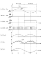
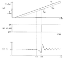
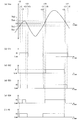
- FIG. 5A shows the transition of the detected voltage Vac and the DC voltage Vdc.
- FIG. 5B shows the transition of the first and fourth gate signals GS1 and GS4, and
- FIG. 5C shows the transition of the second and third gate signals GS2 and GS3.
- FIG. 5D shows the transition between the fifth gate signal GS5 and the inverted signal of the sixth gate signal GS6.
- FIG. 5 (e) shows the transition of the command current ILa *
- FIG. 5 (f) shows the transition of the reactor current ILr.
- FIG. 5 (g) shows the transition of the output current Iac.
- the command current ILa * calculated by the control device 30 has a waveform in which a positive half wave of a sine wave is repeated in a period T / 2.
- the value of the command current ILa * changes according to the waveform of the detection voltage Vac.
- the control device 30 controls the reactor current ILr to the command current ILa * by the peak current mode control, so that the fifth and sixth gate signals GS5 and GS6 are turned on in one switching cycle Tsw.
- the duty ratio Ton / Tsw indicating the ratio is changed.
- the reactor current ILr in one switching cycle Tsw becomes a value corresponding to the duty ratio of the fifth switch. Therefore, the average value Iave of the reactor current ILr is close to the command current ILa *.
- the control device 30 changes the duty ratio of the fifth and sixth gate signals GS5 and GS6 in order to control the reactor current ILr to the command current ILa * by the peak current mode control.
- the detected voltage Vac may be out of phase with respect to the actual voltage Vr.
- the phase shift of the detected voltage Vac with respect to the actual voltage Vr is caused by manufacturing variations of the elements constituting the AC voltage sensor 23 and temperature characteristics. Further, the phase shift of the detected voltage Vac with respect to the actual voltage Vr is also caused by the low-pass filter 243 included in the differential amplification unit 233 of the AC voltage sensor 23 acting as a capacitance component.
- the timing at which the detected voltage Vac becomes the reference voltage Vs deviates from the zero cross timing of the actual voltage Vr.
- the switching timing of the on / off operation of the first to fourth switch elements SW1 to SW4 constituting the full bridge circuit 12 deviates from the timing at which the polarity of the actual voltage Vr is switched, and the first and second AC side terminals TA1 and TA2 Overcurrent may flow in.
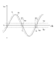
- FIG. 6A shows the transition of the detected voltage Vac and the actual voltage Vr
- FIG. 6B shows the transition of the first and fourth gate signals GS1 and GS4.
- FIG. 6C shows the transition of the second and third gate signals GS2 and GS3, and
- FIG. 6D shows the transition of the output current Iac.
- FIG. 7A is a diagram showing a flow path of a current flowing through the full bridge circuit 12 and the AC power supply 200 during the period P11 of FIG. Note that FIG. 6A shows the detected voltage Vac and the actual voltage Vr when the reference voltage Vs is set to zero for ease of explanation.
- FIG. 7B is a diagram illustrating a current flowing through the full bridge circuit 12 and the AC power supply 200 during the period P12 of FIG.
- the detection voltage Vac shown by the solid line in FIG. 6A has a phase lag behind the actual voltage Vr shown by the broken line.
- the falling timings of the first and fourth gate signals GS1 and GS4 are delayed by ⁇ from the zero cross timing of the actual voltage Vr.
- the rising timing of the second and third gate signals GS2 and GS3 is delayed by ⁇ from the zero cross timing of the actual voltage Vr.
- the actual voltage Vr is negative, while the detected voltage Vac detected by the AC voltage sensor 23 is higher than 0 (reference voltage Vs).
- the body diode D3 of the third switch SW3 and the first switch are generated by the negative actual voltage Vr applied between the first and second AC side terminals TA1 and TA2.
- a first current I1 flows from the first AC side terminal TA1 in the direction of the second AC side terminal TA2 via the AC power supply 200 in the closed circuit including between the drain and the source of the SW1.
- the closed circuit including the drain source of the fourth switch SW4 and the body diode D2 of the second switch SW2 is connected to the closed circuit from the first AC side terminal TA1 via the AC power supply 200. 2
- the second current I2 flows in the direction of the AC side terminal TA2. Therefore, in the period P11, as shown in FIG. 6D, the first current I1 and the second current I2 are added together to cause an overcurrent to flow.
- the rising timings of the first and fourth gate signals GS1 and GS4 are delayed by ⁇ from the zero cross timing of the actual voltage Vr. Further, in the period P12, the falling timings of the second and third gate signals GS2 and GS3 are delayed by ⁇ from the zero cross timing of the actual voltage Vr. Further, in the period P12, the actual voltage Vr is positive, while the detected voltage Vac detected by the AC voltage sensor 23 is negative, which is lower than 0 (reference voltage Vs).
- the body diode D1 of the first switch SW1 and the third switch are generated by the positive actual voltage Vr applied between the first and second AC side terminals TA1 and TA2.
- a third current I3 flows from the second AC side terminal TA2 in the direction of the first AC side terminal TA1 via the AC power supply 200 in the closed circuit including between the drain and the source of the SW3.
- a positive actual voltage Vr is used to connect the drain and source of the second switch SW2 and the body diode D4 of the fourth switch SW4 to a closed circuit from the second AC terminal TA2 via the AC power supply 200.
- the fourth current I4 flows in the direction of the AC side terminal TA1. Therefore, in the period P12, the third current I3 and the fourth current I4 are added together to cause an overcurrent to flow.
- the detected voltage Vac at the zero cross timing of the actual voltage Vr becomes a value different from the reference voltage Vs.
- the detected voltage Vac is lower than the reference voltage Vs at the zero-up cross timing of the actual voltage Vr, and higher than the reference voltage Vs at the zero-down cross timing of the actual voltage Vr. It is a value. Therefore, in the present embodiment, the determination value used for determining the polarity of the actual voltage Vr is determined in consideration of the phase shift of the detected voltage Vac with respect to the actual voltage Vr.
- the polarity determination unit 55 includes the first determination value output unit 60, the second determination value output unit 61, the first comparison unit 62, and the second comparison unit 63. It includes a determination signal output unit 64.
- the first determination value output unit 60 outputs the first determination value Th1 used for determining the polarity of the actual voltage Vr.
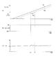
- the first determination value Th1 is a voltage value for determining that the phase of the actual voltage Vr is the zero-up cross timing, and in the present embodiment, as shown in FIG. 8A, it is higher than the reference voltage Vs. It is set to a small value.
- the second determination value output unit 61 outputs the second determination value Th2 used for determining the polarity of the actual voltage Vr.
- the second determination value Th2 is a voltage value for determining that the phase of the actual voltage Vr is the zero down cross timing, and in the present embodiment, as shown in FIG. 8A, it is larger than the reference voltage Vs. It is set to a large value.
- the detection voltage Vac is input to the non-inverting input terminal of the first comparison unit 62, and the first determination value Th1 is input to the inverting input terminal.
- the first comparison unit 62 outputs the first comparison signal CS1 in the high state when the detection voltage Vac is larger than the first determination value Th1, and the detection voltage Vac. Is equal to or less than the first determination value Th1, the first comparison signal CS1 in the low state is output.
- the detection voltage Vac is input to the non-inverting input terminal of the second comparison unit 63, and the second determination value Th2 is input to the inverting input terminal. As shown in FIG.
- the second comparison unit 63 outputs the second comparison signal CS2 in the high state when the detection voltage Vac is larger than the second determination value Th2, and the detection voltage Vac Is equal to or less than the second determination value Th2, the second comparison signal CS2 in the low state is output.
- the first comparison signal CS1 and the second comparison signal CS2 are input to the determination signal output unit 64.
- the determination signal output unit 64 changes the polarity determination signal PS from the low state to the high state when the first comparison signal CS1 is switched from the low state to the high state.
- the determination signal output unit 64 changes the polarity determination signal PS from the high state to the low state when the second comparison signal CS2 is switched from the high state to the low state. Therefore, the determination signal output unit 64 determines that the period from when the detection voltage Vac exceeds the first determination value Th1 to when it falls below the second determination value Th2 is the period when the actual voltage Vr is positive.
- the determination signal output unit 64 determines that the period from when the detection voltage Vac falls below the second determination value Th2 to when it exceeds the first determination value Th1 is a period during which the actual voltage Vr is negative.
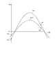
- FIG. 9A shows the transition of the detected voltage Vac near the zero-up cross timing of the actual voltage Vr
- FIG. 9B shows the transition between the first gate signal GS1 and the second gate signal GS2.
- the second gate signal GS2 is shown by a broken line.
- FIG. 9C shows a change in the output current Iac flowing through the full bridge circuit 12. Note that FIG. 9A shows the actual voltage Vr and the detection voltage Vac when the reference voltage Vs is set to zero for the sake of simplicity.
- the phase of the actual voltage Vr is zero-up cross timing.
- the detected voltage Vac is out of phase with the actual voltage Vr, and remains lower than the reference voltage Vs at time t1.
- the detection voltage Vac rises to the reference voltage Vs.
- the actual voltage Vr is positive, whereas the detected voltage Vac is lower than the reference voltage Vs.
- the first determination value Th1 is set to a value lower than the reference voltage Vs, the detected voltage Vac exceeds the first determination value Th1 after the time t1, and the actual voltage Vr becomes positive. It has been determined that Therefore, after the time t1, the first gate signal GS1 is in the high state and the second gate signal GS2 is in the low state in accordance with the switching timing of the polarity of the actual voltage Vr. As a result, overcurrent is suppressed from flowing through the full bridge circuit 12.
- FIG. 10 is a diagram showing processing of the control device 30 of the comparative example.
- the first and second determination values Th1 and Th2 are set as the reference voltage Vs. 10 (a) to 10 (c) correspond to FIGS. 9 (a) to 9 (c).
- the phase of the actual voltage Vr is the zero-up cross timing at the time t11. In the period from time t11 to time t12, the detection voltage Vac is lower than the reference voltage Vs.
- the detection voltage Vac is smaller than the first determination value Th1 and the actual voltage Vr is determined to be negative during the period from time t11 to time t12. That is, in the period from time t11 to time t12, the actual voltage Vr is positive, whereas the determination result of the actual voltage Vr by the polarity determination unit 55 is negative. Therefore, the first gate signal GS1 is in the low state, the second gate signal GS2 is in the high state, and an overcurrent flows through the full bridge circuit 12.
- the deviation width ⁇ i is a value obtained by subtracting the average value Iave of the reactor current ILr from the pre-correction command current IL *.
- D indicates the duty ratio of the fifth switch SW5 during the on period.
- the maximum increase ⁇ slope of the slope compensation signal Slope can be calculated by the following equation (4).
- ⁇ slope ms ⁇ D ⁇ Tsw... (4)
- the average value of the slope ms may be used.
- the duty ratio D during the ON period of the fifth switch SW5 can be calculated by the following formula (5) using the effective value Vrms of the detected voltage Vac.
- the deviation width ⁇ i is calculated as the above formula (1) by the above formulas (2) to (5).
- the reference correction value Ih is calculated using the deviation width ⁇ i represented by the above formula (1). For example, a value obtained by multiplying the deviation width ⁇ i by the calculation coefficient ⁇ can be used as the reference correction value Ih.
- the calculation coefficient ⁇ can be a value greater than 0 and less than or equal to 1. Then, by recording each calculated reference correction value Ih for each effective value Vrms, a reference correction value map can be created.
- the control device 30 determines the polarity of the actual voltage Vr by using the first and second determination values Th1 and Th2, which are different values from the reference voltage Vs of the AC voltage sensor 23.
- the control device 30 determines that the period from when the detection voltage Vac exceeds the first determination value Th1 to when it falls below the second determination value Th2 is the period when the actual voltage Vr is positive, and the detection voltage Vac is the second determination.
- the period from when the value falls below Th2 to when it exceeds the first determination value Th1 is determined as the period during which the actual voltage Vr is negative.
- the reference voltage generation unit 231 may be any one that generates the reference voltage Vs, and may be a switching power supply as well as a voltage dividing circuit using a resistor.
- the first and second determination values Th1 and Th2 are variably set in consideration of the difference in the amplitude and frequency of the detection voltage Vac and the change in the detection voltage Vac due to the sudden voltage fluctuation of the actual voltage Vr. ..
- the polarity determination unit 55 includes an amplitude detection unit 70, a frequency detection unit 71, a first determination value output unit 72, a second determination value output unit 73, and a third. Judgment value output unit 74, fourth judgment value output unit 75, first comparison unit 76, second comparison unit 77, third comparison unit 78, fourth comparison unit 79, and determination signal output unit 80. It has.
- the amplitude detection unit 70 detects the amplitude ⁇ A of the detection voltage Vac. For example, the amplitude detection unit 70 detects the difference between the maximum value or the minimum value and the median value as the amplitude ⁇ A of the detection voltage Vac in one cycle T of the detection voltage Vac detected by the AC voltage sensor 23.
- the frequency detection unit 71 detects the frequency F of the detection voltage Vac based on the detection voltage Vac.
- the output frequency of the AC power supply 200 is either a first frequency or a second frequency higher than the first frequency.
- the first frequency is 50 Hz and the second frequency is 60 Hz.
- the first determination value output unit 72 sets the first determination value Th1 ( ⁇ Vs) to a smaller value as the amplitude ⁇ A detected by the amplitude detection unit 70 increases. This is because as the amplitude ⁇ A increases, the slope of the detection voltage Vac increases, and the deviation width from the reference voltage Vs to the detection voltage Vac detected at the zero-up cross timing of the actual voltage Vr increases on the negative side. is there.
- the voltages corresponding to the zero-up cross timing of the actual voltage Vr in the two detection voltages Vac1 and Vac2 having different amplitudes ⁇ A are shown as the zero-up side detection voltages Vu1 and Vu2.
- the zero-up side detection voltage Vu1 at the detection voltage Vac1 having the larger amplitude is smaller than the zero-up side detection voltage Vu2 at the detection voltage Vac2 having the smaller amplitude.
- the second determination value output unit 73 sets the second determination value Th2 to a larger value as the amplitude ⁇ A detected by the amplitude detection unit 70 increases. This is because as the amplitude ⁇ A increases, the slope of the detection voltage Vac increases, and the deviation width from the reference voltage Vs to the detection voltage Vac detected at the zero-down cross timing of the actual voltage Vr increases to the positive side. is there.
- the voltages corresponding to the zero-down cross timing of the actual voltage Vr in the two detection voltages Vac1 and Vac2 having different amplitudes ⁇ A are shown as the zero-down side detection voltages Vd1 and Vd2.
- the zero-down side detection voltage Vd1 at the detection voltage Vac1 having the larger amplitude is larger than the zero-down side detection voltage Vd2 at the detection voltage Vac2 having the smaller amplitude.
- the first determination value output unit 72 variably sets the first determination value Th1 based on the frequency F detected by the frequency detection unit 71. Further, the second determination value output unit 73 variably sets the second determination value Th2 based on the frequency F detected by the frequency detection unit 71. This is because the slope of the detection voltage Vac changes according to the frequency F of the detection voltage Vac, and the zero-down side detection voltage and the zero-up side detection voltage have different values.
- the third determination value output unit 74 outputs the third determination value Th3, which is an intermediate determination value between the first determination value Th1 and the second determination value Th2.
- the fourth determination value output unit 75 outputs the fourth determination value Th4, which is an intermediate determination value between the first determination value Th1 and the second determination value Th2.
- the fourth determination value Th4 is set in preparation for a case where the detection voltage Vac falls below the second determination value Th2 due to a sudden voltage fluctuation of the actual voltage Vr and then starts to increase without sufficiently decreasing. To. If the detected voltage Vac does not exceed the first determination value Th1 within the next half cycle, the polarity of the actual voltage Vr remains erroneously determined, and an overcurrent continues to flow in the power conversion device 100.
- the third determination value Th3 is set to a value lower than the reference voltage Vs
- the fourth determination value Th4 is set to a value higher than the reference voltage Vs.
- the third determination value output unit 74 sets the third determination value Th3 to a smaller value as the detected amplitude ⁇ A increases.
- the fourth determination value output unit 75 sets the fourth determination value Th4 to a larger value as the detected amplitude ⁇ A increases.
- the third and fourth determination value output units 74 and 75 variably set the third and fourth determination values Th3 and Th4 based on the detected frequency F.
- the first to fourth determination value output units 72 to 75 are determination values indicating the relationship between the combination of the amplitude ⁇ A and the frequency F at the detection voltage Vac and the first to fourth determination values Th1 to Th4. It has a map. By referring to this determination value map, the first to fourth determination value output units 72 to 75 obtain the first to fourth determination values Th1 to Th4 according to the combination of the amplitude ⁇ A and the frequency F in the detection voltage Vac. Can be output.
- the detection voltage Vac and the first determination value Th1 are input to the first comparison unit 76, and the detection voltage Vac and the second determination value Th2 are input to the second comparison unit 77.
- the detection voltage Vac is input to the non-inverting input terminal of the third comparison unit 78, and the third determination value Th3 is input to the inverting input terminal.
- the detection voltage Vac is input to the non-inverting input terminal of the fourth comparison unit 79, and the fourth determination value Th4 is input to the inverting input terminal.
- the third comparison unit 78 outputs a high-state third comparison signal CS3 when the detection voltage Vac is larger than the third determination value Th3, and when the detection voltage Vac is less than or equal to the third determination value Th3.
- the third comparison signal CS3 in the low state is output to.
- the fourth comparison unit 79 outputs a high-state fourth comparison signal CS4 when the detection voltage Vac is larger than the fourth determination value Th4, and when the detection voltage Vac is the fourth determination value Th4 or less.
- the fourth comparison signal CS4 in the low state is output to.
- the first to fourth comparison signals CS1 to CS4 from the first to fourth comparison units 76 to 79 are input to the determination signal output unit 80.
- the determination signal output unit 80 changes the polarity determination signal PS from the low state to the high state. Further, the determination signal output unit 80 changes the polarity determination signal PS from the high state to the low state when the second comparison signal CS2 changes from the high state to the low state.
- the determination signal output unit 80 changes the polarity determination signal PS from the high state to the low state when the third comparison signal CS3 changes from the high state to the low state when the first comparison signal CS1 is in the high state. As a result, the determination signal output unit 80 determines the polarity when the detection voltage Vac exceeds the first determination value Th1 and then the detection voltage Vac falls below the third determination value without falling below the second determination value Th2. The PS is changed to the low state, and it is determined that the actual voltage Vr has switched from the positive electrode property to the negative electrode property.
- the determination signal output unit 80 changes the polarity determination signal PS from the low state to the high state when the fourth comparison signal CS4 changes from the low state to the high state when the second comparison signal CS2 is in the low state. As a result, the determination signal output unit 80 determines the polarity when the detection voltage Vac falls below the second determination value Th2 and then exceeds the fourth determination value Th4 without exceeding the first determination value Th1. It is determined that the signal PS is changed to the high state and the actual voltage Vr is switched from the negative electrode property to the positive electrode property.
- FIG. 14 shows the first to fourth comparison signals CS1 to CS4 and the polarity determination signal PS when the detection voltage Vac starts to increase and then decreases without increasing to a predetermined amplitude amount due to a sudden voltage fluctuation. It is a figure explaining a change.
- FIG. 14A shows the detection voltage Vac
- FIG. 14B shows the first comparison signal CS1.
- FIG. 14 (c) shows the second comparison signal CS2, and
- FIG. 14 (d) shows the third comparison signal CS3.
- FIG. 14 (e) shows the fourth comparison signal CS4, and
- FIG. 14 (f) shows the polarity determination signal PS.
- the first comparison signal CS1 changes from the low state to the high state.
- the polarity determination signal PS changes from the low state to the high state.
- the third comparison signal CS3 and the fourth comparison signal CS4 change in order from the low state to the high state.
- the detection voltage Vac does not exceed the second determination value Th2, and changes from an increase to a decrease.
- the fourth comparison signal CS4 changes from the high state to the low state.
- the third comparison signal CS3 changes from the high state to the low state. Therefore, at time t24, the first comparison signal CS1 is in the high state, and the third comparison signal CS3 changes from the high state to the low state, so that the polarity determination signal PS changes from the high state to the low state. It is determined that the actual voltage Vr has switched from the positive electrode property to the negative electrode property.
- the first comparison signal CS1 changes from the high state to the low state.
- the detection voltage Vac changes from a decrease to an increase
- the detection voltage Vac exceeds the first determination value Th1 at time t26, so that the first comparison signal CS1 changes from the low state to the high state.
- the polarity determination signal PS changes from the low state to the high state, and the actual voltage Vr is switched from the negative electrode property to the positive electrode property.
- the detection voltage Vac exceeds the third judgment value Th3, the fourth judgment value Th4, and the second judgment value Th2 in order, so that the third comparison signal CS3, the fourth comparison signal CS4, and the second comparison
- the signal CS2 changes from the low state to the high state in order.
- the detection voltage Vac changes from rising to falling, the detection voltage Vac falls below the second determination value Th2, so that the second comparison signal CS2 changes from the high state to the low state.
- the polarity determination signal PS changes from the high state to the low state, and the actual voltage Vr is switched from the positive electrode property to the negative electrode property.
- the detection voltage Vac falls below the fourth judgment value Th4, the third judgment value Th3, and the first judgment value Th1 in this order, so that the fourth comparison signal CS4, the third comparison signal CS3, and the third comparison signal CS3 1
- the comparison signal CS1 changes from a high state to a low state in order.
- FIG. 15 shows the first to fourth comparison signals CS1 to CS4 and the polarity determination signal PS when the detection voltage Vac starts to decrease and then increases without decreasing to a predetermined amplitude amount due to a sudden voltage fluctuation. It is a figure explaining a change. 15 (a) to 15 (f) correspond to FIGS. 14 (a) to 14 (f), respectively.
- the changes in the first to fourth comparison signals CS1 to CS4 and the polarity determination signal PS during the period from time t40 to time t45 are the changes in the first to fourth comparison signals CS1 to CS4 from time t26 to time t31 in FIG. And since it is the same as the change of the polarity determination signal PS, the description thereof will be omitted.
- the fourth comparison signal CS4 changes from the high state to the low state, and then the detection voltage Vac changes from a decrease to an increase.
- the detection voltage Vac does not fall below the first and third determination values Th1 and Th3, but exceeds the fourth determination value Th4 at time t46, and the fourth comparison signal CS4 changes from the low state to the high state.
- the second comparison signal CS2 is in the low state and the fourth comparison signal CS4 is changing from the low state to the high state, so that the polarity determination signal PS changes from the low state to the high state.
- the second comparison signal CS2 changes from the low state to the high state.
- the detection voltage Vac changes from rising to falling, it falls below the second determination value Th2 at time t48, so that the second comparison signal CS2 changes from a high state to a low state.
- the polarity determination signal PS changes from the high state to the low state, and the actual voltage Vr is switched from the positive electrode property to the negative electrode property.
- the detection voltage Vac falls below the fourth determination value Th4, the third determination value Th3, and the first determination value Th1 in that order, so that the fourth comparison signal CS4, the third comparison signal CS3, and the third comparison signal CS3 are generated.
- the comparison signal CS1 is sequentially changing from the high state to the low state.
- the polarity determination unit 55 determines that the acquired detection voltage Vac exceeds the first determination value Th1 and then falls below the third determination value Th3 without falling below the second determination value Th2, the polarity of the actual voltage Vr becomes It is determined that the positive electrode property has been switched to the negative electrode property. Further, when the polarity determination unit 55 determines that the detected voltage Vac has fallen below the second determination value Th2 and then exceeds the fourth determination value Th4 without exceeding the first determination value Th1, the polarity of the actual voltage Vr becomes high. It is determined that the negative electrode property has been switched to the positive electrode property. This makes it possible to prevent a state in which the polarity of the actual voltage Vr is continuously erroneously determined due to a sudden voltage fluctuation of the actual voltage Vr.
- the polarity determination unit 55 variably sets the first determination value Th1 and the second determination value Th2 based on the amplitude ⁇ A of the detection voltage Vac.
- an overcurrent flows through the AC side terminals TA1 and TA2 even when the zero-up side detection voltage Vu and the zero-down side detection voltage Vd deviate from the reference voltage Vs due to the increase / decrease in the amplitude ⁇ A of the actual voltage Vr. Can be suppressed.
- the polarity determination unit 55 variably sets the first determination value Th1 and the second determination value Th2 based on the frequency F of the detection voltage Vac. As a result, even if the zero-up side detection voltage Vu and the zero-down side detection voltage Vd deviate from the reference voltage Vs due to the increase or decrease of the frequency F of the actual voltage Vr, an overcurrent flows through the AC side terminals TA1 and TA2. Can be suppressed.
- the first comparison unit 76 into which the first determination value Th1 is input and the fourth comparison unit 79 in which the fourth determination value Th4 is input are shared, and the second determination value Th2 is input.
- the second comparison unit 77 and the third comparison unit 78 into which the third determination value Th3 is input may be shared.
- the first and fourth determination value output units 72 and 75 detect the timing T1 in which the detection voltage Vac falls below the reference voltage Vs. Then, the fourth determination value output unit 75 inputs the fourth determination value Th4 to the first comparison unit 76 in the predetermined first switching period SP1 including the detected timing T1 in one cycle T of the detection voltage Vac. .. Further, the first determination value output unit 72 may input the first determination value Th1 to the first comparison unit 76 in a period other than the first switching period SP1 in one cycle T of the detection voltage Vac. The second and third determination value output units 73 and 74 detect the timing T2 in which the detection voltage Vac exceeds the reference voltage Vs.
- the third determination value output unit 74 inputs the third determination value Th3 to the second comparison unit 77 in a predetermined second switching period SP2 including the detected timing T2 in one cycle of the detection voltage Vac. Further, the second determination value output unit 73 may input the second determination value Th2 to the second comparison unit 77 in a period other than the second switching period SP2 in one cycle of the detection voltage Vac.
- the first comparison unit 76 outputs the first comparison signal CS1 in a period other than the first switching period SP1 in one cycle T of the detection voltage Vac, and outputs the fourth comparison signal CS4 in the first switching period SP1. To do.
- the second comparison unit 77 outputs the second comparison signal CS2 in a period other than the second switching period SP2 in one cycle T of the detection voltage Vac, and outputs the third comparison signal CS3 in the second switching period SP2. To do.
- the control device 30 corrects the first and second determination values Th1 and Th2 according to the average value of the output current Iac in the predetermined period including the timing when the detection voltage Vac becomes the reference voltage Vs.
- the polarity determination unit 55 shown in FIG. 17 includes a first average current calculation unit 81, a second average current calculation unit 82, a first current correction unit 83, a second current correction unit 84, and a first limiter 85.
- a second limiter 86, a first abnormality determination unit 87, and a second abnormality determination unit 88 are provided.
- the control device 30 has a function as a current acquisition unit.
- the output current Iac and the polarity determination signal PS from the determination signal output unit 64 are input to the first average current calculation unit 81 and the second average current calculation unit 82.
- the first average current calculation unit 81 calculates the zero-up side average current, which is the average value of the output current Iac in a predetermined period including the timing when the polarity determination signal PS switches from the low state to the high state.
- the second average current calculation unit 82 calculates the zero-down side average current, which is the average value of the output current Iac in a predetermined period including the timing when the polarity determination signal PS switches from the high state to the low state.
- the first and second average current calculation units 81 and 82 acquire a plurality of output currents Iac in the predetermined period in one cycle T of the detection voltage Vac.
- the first average current calculation unit 81 calculates the zero-up side average current based on the acquired plurality of output currents Iac.
- the second average current calculation unit 82 calculates the zero-down side average current based on the acquired plurality of output currents Iac.
- the resonance current associated with the on / off operation of the first to fourth switches SW1 to SW4 may flow through the full bridge circuit 12. Therefore, the output current Iac used for calculating the average current is preferably a value in the above-mentioned predetermined period in which the resonance current does not flow in the full bridge circuit 12.
- the calculated zero-up side average current is input to the first current correction unit 83.
- the first current correction unit 83 calculates the first determination value Th1 for bringing the average current on the zero-up side closer to zero. Specifically, the first current correction unit 83 calculates the first determination value Th1 as an operation amount for feedback-controlling the zero-up side average current to zero. In this embodiment, integral control is used as feedback control. By the processing of the first current correction unit 83, the first determination value Th1 is corrected so that the average current on the zero-up side approaches zero.
- the calculated zero-down side average current is input to the second current correction unit 84.
- the second current correction unit 84 calculates the second determination value Th2 for bringing the average current on the zero-down side closer to zero. Specifically, the second current correction unit 84 calculates the second determination value Th2 as an operation amount for feedback-controlling the zero-down side average current to zero. In this embodiment, integral control is used as feedback control. By the processing of the second current correction unit 84, the second determination value Th2 is corrected so that the average current on the zero-down side approaches zero.
- the first determination value Th1 calculated by the first current correction unit 83 is input to the inverting input terminal of the first comparison unit 62 after the upper limit value or the lower limit value is limited by the first limiter 85.
- the second determination value Th2 calculated by the second current correction unit 84 is input to the inverting input terminal of the second comparison unit 63 after the upper limit value or the lower limit value is limited by the second limiter 86.
- the determination signal output unit 64 determines the polarity of the actual voltage Vr based on the first comparison signal CS1 from the first comparison unit 62 and the second comparison signal CS2 from the second comparison unit 63.
- the first determination value Th1 is also input to the first abnormality determination unit 87.
- the first abnormality determination unit 87 is in an abnormal state in which the first determination value Th1 is not normally calculated when the absolute value of the first determination value Th1 is larger than the predetermined first abnormality determination value J1. Is determined.
- the second determination value Th2 is also input to the second abnormality determination unit 88.
- the second abnormality determination unit 88 is in an abnormal state in which the second determination value Th2 is not normally calculated when the absolute value of the second determination value Th2 is larger than the predetermined second abnormality determination value J2. Is determined.
- the polarity determination unit 55 determines the abnormality of the first and second determination values Th1 and Th2, the polarity determination unit 55 does not perform the polarity determination of the actual voltage Vr using the first and second determination values Th1 and Th2.
- the operation of the power conversion device 100 may be stopped.
- the first and second determination values Th1 and Th2 are corrected based on the average value of the output current Iac in a predetermined period including the timing when the polarity of the actual voltage Vr is determined to be switched. As a result, it is possible to suppress a shift in the timing at which the set to be turned on is switched between the set of the first and fourth switches SW1 and SW4 and the set of the second and third switches SW2 and SW3 in real time.
- the control device 30 determines whether or not the first and second determination values Th1 and Th2 are in an abnormal state in which they are not normally calculated. Thereby, for example, it is possible to prevent the power conversion device 100 from continuing to operate in a state where an abnormality has occurred in the power conversion device 100.
- the polarity determination unit 55 uses one output current Iac detected in a predetermined period including the timing when it is determined that the polarity of the actual voltage Vr is switched instead of the zero-up side average current and the zero-down side average current. 2
- the determination values Th1 and Th2 may be corrected.
- the first current correction unit 83 corrects the first determination value Th1 based on one output current Iac detected near the timing when the actual voltage Vr is determined to have switched from the negative electrode property to the positive electrode property.
- the second current correction unit 84 may correct the second determination value Th2 based on one output current Iac detected in the vicinity of the timing when the actual voltage Vr is determined to have switched from the positive electrode property to the negative electrode property.
- the phenomenon that the timing at which the detection voltage Vac becomes the reference voltage Vs deviates from the zero cross timing of the actual voltage Vr is due to the fact that the detection voltage Vac includes an offset error and the detection voltage Vac is offset up and down with respect to the actual voltage Vr. Also occurs.
- the detected voltage Vac is offset up and down with respect to the actual voltage Vr, the first period P1 in which the detected voltage Vac becomes positive and the second period P2 in which the detected voltage Vac becomes negative in one cycle T of the detected voltage Vac.
- the polarity determination unit 55 corrects the first determination value Th1 and the second determination value Th2 based on the difference between the first period P1 and the second period P2 in the one cycle T of the detection voltage Vac. To do.
- the polarity determination unit 55 shown in FIG. 18 includes a positive period detection unit 90, a negative period detection unit 91, a period difference calculation unit 92, a first period difference correction unit 93, and a second period difference correction unit 94. Is equipped with.
- the polarity determination signal PS from the determination signal output unit 64 is input to the positive electrode period detection unit 90.
- the positive electrode period detection unit 90 detects the length in which the polarity determination signal PS is in the high state in one cycle T of the detection voltage Vac as the length of the first period P1 in the one cycle T of the detection voltage Vac.
- the polarity determination signal PS from the determination signal output unit 64 is input to the negative electrode period detection unit 91.
- the negative electrode period detection unit 91 detects the length in which the polarity determination signal PS is in the low state in one cycle T of the detection voltage Vac as the length of the second period P2 in the one cycle T of the detection voltage Vac.
- the detected length of the first period P1 and the length of the second period P2 are input to the period difference calculation unit 92.
- the period difference calculation unit 92 outputs a value obtained by subtracting the length of the second period P2 from the length of the first period P1 as an offset determination value.
- the calculated offset determination value is input to the first period difference correction unit 93.
- the first period difference correction unit 93 calculates the first determination value Th1 for bringing the offset determination value closer to zero. Specifically, the first period difference correction unit 93 calculates the first determination value Th1 as an operation amount for feedback-controlling the offset determination value to zero. In this embodiment, integral control is used as feedback control. By the processing of the first period difference correction unit 93, the first determination value Th1 is corrected so that the offset determination value approaches zero.
- the calculated offset determination value is also input to the second period difference correction unit 94.
- the second period difference correction unit 94 calculates the second determination value Th2 for bringing the offset determination value closer to zero. Specifically, the second period difference correction unit 94 calculates the second determination value Th2 as an operation amount for feedback-controlling the offset determination value to zero. In this embodiment, integral control is used as feedback control. By the processing of the second period difference correction unit 94, the second determination value Th2 is corrected so that the offset determination value approaches zero.
- the calculated first and second determination values Th1 and Th2 are input to the first and second comparison units 62 and 63 after the upper limit value or the lower limit value is limited by the first and second limiters 85 and 86. ..
- the determination signal output unit 64 determines the polarity of the actual voltage Vr based on the first comparison signal CS from the first comparison unit 62 and the second comparison signal CS2 from the second comparison unit 63.
- the first determination value Th1 is also input to the first abnormality determination unit 87
- the second determination value Th2 is also input to the second abnormality determination unit 88.
- the first and second abnormality determination units 87 and 88 determine the presence or absence of an abnormal state based on the first and second determination values Th1 and Th2.
- the polarity determination unit 55 may correct the first determination value Th1 and the second determination value Th2 based on the ratio of the second period P2 to the first period P1 in the one cycle T of the detection voltage Vac. In this case, the polarity determination unit 55 may use the ratio of the second period P2 to the first period P1 in one cycle of the detection voltage Vac as the offset determination value.
- the first and second determination values Th1 and Th2 are corrected based on the voltage difference between the reference voltage Vs and the first and second determination values Th1 and Th2.
- the control device 30 corrects the normal drive mode for converting power between the DC voltage and the AC voltage and the first and second determination values Th1 and Th2 as the drive modes for the power conversion device 100. It is possible to switch between the diagnostic mode.
- the control device 30 corrects the first and second determination values Th1 and Th2 according to the present embodiment in the diagnostic mode. Further, when the control device 30 executes the diagnostic mode, as shown in FIG. 19, the AC power supply 200 is not connected to the power conversion device 100. That is, in the diagnostic mode, the detection voltage Vac when the actual voltage Vr becomes zero is used as the reference voltage Vs.
- the polarity determination unit 55 shown in FIG. 20 includes a first determination value output unit 101 and a second determination value output unit 102.
- the first comparison signal CS1 from the first comparison unit 62 is input to the first determination value output unit 101.
- the first determination value output unit 101 calculates the first determination value Th1 for bringing the first comparison signal CS1 output from the first comparison unit 62 closer to zero. Specifically, the first determination value output unit 101 changes the first determination value Th1, and the first determination value Th1 at the timing when the first comparison signal CS1 changes between the low state and the high state. Is set as the corrected first determination value Th1.
- the second comparison signal CS2 output from the second comparison unit 63 is input to the second determination value output unit 102.
- the second determination value output unit 102 calculates the second determination value Th2 for bringing the second comparison signal CS2 from the second comparison unit 63 closer to zero. Specifically, the second determination value output unit 102 changes the second determination value Th2, and the second determination value Th2 at the timing when the second comparison signal CS2 changes between the low state and the high state. Is set as the corrected second determination value Th2.
- the correction of the first and second judgment values Th1 and Th2 by the first and second judgment value output units 101 and 102 is performed over the period during which the diagnostic mode is switched, and the corrected first and second judgments are performed.
- the values Th1 and Th2 are stored in a storage unit (not shown) included in the control device 30. After the drive mode of the power conversion device 100 is switched from the diagnostic mode to the normal drive mode, the first determination value output unit 101 outputs the corrected first determination value Th1 and the second determination value output unit 102. The corrected second determination value Th2 is output from.
- the reference voltage Vs used for correcting the first and second determination values Th1 and Th2 may be detected by the control device 30 in a state where the power conversion device 100 is connected to the AC power supply 200.
- FIG. 21 is a diagram illustrating the configuration of the polarity determination unit 55 in the diagnostic mode according to the present embodiment.
- the reference voltage generation unit 231 of the AC voltage sensor 23 is connected to the control device 30, and the reference voltage Vs generated by the reference voltage generation unit 231 is input to the control device 30.
- the control device 30 may have the configuration shown in FIG. 20.
- the polarity determination unit 55 includes a first determination value output unit 111, a second determination value output unit 112, a first comparison unit 113, and a second comparison unit 114.
- the first determination value Th1 from the first determination value output unit 111 is input to the inverting input terminal of the first comparison unit 113.
- the reference voltage Vs is input to the non-inverting input terminal of the first comparison unit 113.
- the second determination value Th2 from the second determination value output unit 112 is input to the inverting input terminal of the second comparison unit 114.
- the reference voltage Vs is also input to the non-inverting input terminal of the second comparison unit 114.
- the first comparison signal CS1 from the first comparison unit 113 is input to the first determination value output unit 111.
- the first determination value output unit 111 calculates the first determination value Th1 for bringing the first comparison signal CS1 close to zero. By the processing of the first determination value output unit 111, the first determination value Th1 is corrected so that the first comparison signal CS1 approaches zero.
- the second comparison signal CS2 from the second comparison unit 114 is input to the second determination value output unit 112.
- the second determination value output unit 112 calculates the second determination value Th2 for bringing the second comparison signal CS2 closer to zero. By the processing of the second determination value output unit 112, the second determination value Th2 is corrected so that the second comparison signal CS2 approaches zero.
- the first and second judgment values Th2 are used as the corrected voltage judgment value in the first comparison unit and the second comparison unit. It may be entered. In this case, when the first determination value Th1 is input to the first and second comparison units, the second determination value output unit may be deleted. Further, when the second determination value Th2 is input to the first and second comparison units, the first determination value output unit may be deleted.
- the polarity determination unit 55 may include an abnormality determination unit that determines that the power conversion device is abnormal when the corrected first and second determination values Th1 and Th2 are larger than the abnormality determination value.
- the first to fourth switches SW1 to SW4 may be IGBTs.
- a freewheel diode is connected in antiparallel to the first to fourth switches SW1 to SW4 instead of the body diode.
- the power conversion device 100 is a bidirectional power conversion device that converts one of the input voltage of the DC voltage and the AC voltage into the other voltage, in addition to the one that converts the DC voltage into the AC voltage. There may be.
- the sixth switch SW6 corresponds to a drive switch.
- the control device 30 outputs the fifth gate signal GS5 by the average current mode control instead of outputting the fifth gate signal GS5 for operating the fifth switch SW5 by the peak current mode control. There may be.
- the controls and techniques described in this disclosure are provided by a dedicated computer provided by configuring a processor and memory programmed to perform one or more functions embodied by a computer program. It may be realized. Alternatively, the controls and methods thereof described in the present disclosure may be implemented by a dedicated computer provided by configuring the processor with one or more dedicated hardware logic circuits. Alternatively, the control unit and method thereof described in the present disclosure may be a combination of a processor and memory programmed to perform one or more functions and a processor composed of one or more hardware logic circuits. It may be realized by one or more dedicated computers configured. Further, the computer program may be stored in a computer-readable non-transitional tangible recording medium as an instruction executed by the computer.
Landscapes
- Engineering & Computer Science (AREA)
- Power Engineering (AREA)
- Inverter Devices (AREA)
Priority Applications (2)
| Application Number | Priority Date | Filing Date | Title |
|---|---|---|---|
| CN202080030739.0A CN113785484B (zh) | 2019-04-25 | 2020-04-23 | 电力转换装置的控制装置 |
| US17/507,938 US11923756B2 (en) | 2019-04-25 | 2021-10-22 | Control apparatus for power conversion apparatus |
Applications Claiming Priority (2)
| Application Number | Priority Date | Filing Date | Title |
|---|---|---|---|
| JP2019084739A JP7045346B2 (ja) | 2019-04-25 | 2019-04-25 | 電力変換装置の制御装置 |
| JP2019-084739 | 2019-04-25 |
Related Child Applications (1)
| Application Number | Title | Priority Date | Filing Date |
|---|---|---|---|
| US17/507,938 Continuation US11923756B2 (en) | 2019-04-25 | 2021-10-22 | Control apparatus for power conversion apparatus |
Publications (1)
| Publication Number | Publication Date |
|---|---|
| WO2020218442A1 true WO2020218442A1 (ja) | 2020-10-29 |
Family
ID=72942163
Family Applications (1)
| Application Number | Title | Priority Date | Filing Date |
|---|---|---|---|
| PCT/JP2020/017548 Ceased WO2020218442A1 (ja) | 2019-04-25 | 2020-04-23 | 電力変換装置の制御装置 |
Country Status (4)
| Country | Link |
|---|---|
| US (1) | US11923756B2 (enExample) |
| JP (1) | JP7045346B2 (enExample) |
| CN (1) | CN113785484B (enExample) |
| WO (1) | WO2020218442A1 (enExample) |
Families Citing this family (4)
| Publication number | Priority date | Publication date | Assignee | Title |
|---|---|---|---|---|
| JP7161447B2 (ja) | 2019-06-24 | 2022-10-26 | 株式会社Soken | 電力変換装置 |
| KR102387123B1 (ko) * | 2020-07-21 | 2022-04-15 | 한국항공우주연구원 | Ac-dc 컨버터 회로 시스템, 및 ac-dc 컨버터 회로 시스템의 동작 방법 |
| JP7130024B2 (ja) * | 2020-11-12 | 2022-09-02 | 三菱電機株式会社 | 電力変換装置 |
| CN118100655A (zh) * | 2023-12-19 | 2024-05-28 | 浙江艾罗网络能源技术股份有限公司 | 移相控制电路和llc电路的移相控制方法 |
Citations (6)
| Publication number | Priority date | Publication date | Assignee | Title |
|---|---|---|---|---|
| JPH04359695A (ja) * | 1991-06-07 | 1992-12-11 | Daikin Ind Ltd | 位相制御装置 |
| JPH09275685A (ja) * | 1996-02-06 | 1997-10-21 | Mitsubishi Electric Corp | 電源高調波抑制装置 |
| JP2002260833A (ja) * | 2000-12-27 | 2002-09-13 | Mitsui Eng & Shipbuild Co Ltd | 誘導加熱方法および装置 |
| JP2005102489A (ja) * | 2003-08-28 | 2005-04-14 | Matsushita Electric Ind Co Ltd | 電源装置およびそれを用いた空気調和機 |
| JP2015165751A (ja) * | 2014-03-03 | 2015-09-17 | 株式会社豊田自動織機 | 交流電圧の周期及び位相検出装置及び方法 |
| JP2018007326A (ja) * | 2016-06-28 | 2018-01-11 | 日立ジョンソンコントロールズ空調株式会社 | 電力変換装置、及びこれを備える空気調和機 |
Family Cites Families (14)
| Publication number | Priority date | Publication date | Assignee | Title |
|---|---|---|---|---|
| EP1535492B1 (en) | 2002-06-26 | 2013-08-07 | Mitsui Engineering & Shipbuilding Co., Ltd. | Induction heating method and unit |
| DE102008064402B4 (de) * | 2008-12-22 | 2011-03-10 | Texas Instruments Deutschland Gmbh | Gleichrichterschaltung |
| JP5256432B1 (ja) * | 2012-06-27 | 2013-08-07 | 東洋システム株式会社 | フルブリッジ電力変換装置 |
| JP2014241660A (ja) * | 2013-06-11 | 2014-12-25 | ニチコン株式会社 | 電力変換装置 |
| JP6260295B2 (ja) * | 2014-01-23 | 2018-01-17 | サンケン電気株式会社 | 力率改善回路 |
| JP6158739B2 (ja) | 2014-03-31 | 2017-07-05 | 株式会社デンソー | 電力変換装置 |
| JP6497297B2 (ja) * | 2015-07-31 | 2019-04-10 | 株式会社デンソー | 電力変換装置 |
| WO2018186344A1 (ja) * | 2017-04-05 | 2018-10-11 | 住友電気工業株式会社 | 電源装置及び電源装置の制御方法 |
| CN106992688A (zh) * | 2017-06-10 | 2017-07-28 | 张炳耀 | 超大功率zvs+zcs综合软开关dc/dc变换器 |
| JP6936693B2 (ja) * | 2017-10-23 | 2021-09-22 | 株式会社Soken | 電力変換装置 |
| JP6983082B2 (ja) * | 2018-01-25 | 2021-12-17 | 株式会社Soken | Dc・ac変換器の制御装置 |
| JP7054358B2 (ja) * | 2018-03-30 | 2022-04-13 | 株式会社Soken | 電力変換装置の制御装置 |
| JP6898882B2 (ja) * | 2018-04-09 | 2021-07-07 | 株式会社Soken | 電力変換装置の制御装置 |
| JP7157640B2 (ja) * | 2018-11-28 | 2022-10-20 | 株式会社Soken | 電力変換装置の制御装置 |
-
2019
- 2019-04-25 JP JP2019084739A patent/JP7045346B2/ja active Active
-
2020
- 2020-04-23 WO PCT/JP2020/017548 patent/WO2020218442A1/ja not_active Ceased
- 2020-04-23 CN CN202080030739.0A patent/CN113785484B/zh active Active
-
2021
- 2021-10-22 US US17/507,938 patent/US11923756B2/en active Active
Patent Citations (6)
| Publication number | Priority date | Publication date | Assignee | Title |
|---|---|---|---|---|
| JPH04359695A (ja) * | 1991-06-07 | 1992-12-11 | Daikin Ind Ltd | 位相制御装置 |
| JPH09275685A (ja) * | 1996-02-06 | 1997-10-21 | Mitsubishi Electric Corp | 電源高調波抑制装置 |
| JP2002260833A (ja) * | 2000-12-27 | 2002-09-13 | Mitsui Eng & Shipbuild Co Ltd | 誘導加熱方法および装置 |
| JP2005102489A (ja) * | 2003-08-28 | 2005-04-14 | Matsushita Electric Ind Co Ltd | 電源装置およびそれを用いた空気調和機 |
| JP2015165751A (ja) * | 2014-03-03 | 2015-09-17 | 株式会社豊田自動織機 | 交流電圧の周期及び位相検出装置及び方法 |
| JP2018007326A (ja) * | 2016-06-28 | 2018-01-11 | 日立ジョンソンコントロールズ空調株式会社 | 電力変換装置、及びこれを備える空気調和機 |
Also Published As
| Publication number | Publication date |
|---|---|
| JP2020182341A (ja) | 2020-11-05 |
| CN113785484A (zh) | 2021-12-10 |
| US20220045595A1 (en) | 2022-02-10 |
| US11923756B2 (en) | 2024-03-05 |
| CN113785484B (zh) | 2024-04-02 |
| JP7045346B2 (ja) | 2022-03-31 |
Similar Documents
| Publication | Publication Date | Title |
|---|---|---|
| WO2020218442A1 (ja) | 電力変換装置の制御装置 | |
| US10826385B2 (en) | Power factor correction circuit with calculated duty compensation and driving method thereof | |
| US10320310B2 (en) | Power conversion device | |
| JP7157640B2 (ja) | 電力変換装置の制御装置 | |
| EP3758209A1 (en) | Semiconductor device | |
| CN110086367B9 (zh) | 用于控制dc-ac转换器的设备 | |
| CN103328987A (zh) | 极性检测电路 | |
| JP7054358B2 (ja) | 電力変換装置の制御装置 | |
| JP7161447B2 (ja) | 電力変換装置 | |
| US11418128B2 (en) | Control apparatus for electric power conversion apparatus | |
| CN111937288A (zh) | 电力转换装置的控制装置 | |
| CN113273072B (zh) | Dc·ac转换装置的控制装置 | |
| US12166413B2 (en) | Integrated circuit and power supply circuit | |
| TWI634405B (zh) | 電源偵測及傳輸電路以及電源供應器 | |
| WO2019203113A1 (ja) | 電力変換装置の制御装置 | |
| JP7128717B2 (ja) | Dc・ac変換装置の制御装置 | |
| JP6993925B2 (ja) | 電力変換装置の制御装置 | |
| JP2019054616A (ja) | 力率改善回路及び充電器 | |
| CN107276419B (zh) | 电源侦测及传输电路以及电源供应器 | |
| JP2006094631A (ja) | 電源装置 | |
| JP2005124270A (ja) | マトリクスコンバータシステム |
Legal Events
| Date | Code | Title | Description |
|---|---|---|---|
| 121 | Ep: the epo has been informed by wipo that ep was designated in this application |
Ref document number: 20794052 Country of ref document: EP Kind code of ref document: A1 |
|
| NENP | Non-entry into the national phase |
Ref country code: DE |
|
| 122 | Ep: pct application non-entry in european phase |
Ref document number: 20794052 Country of ref document: EP Kind code of ref document: A1 |