WO2020213479A1 - 処理装置及び処理方法 - Google Patents
処理装置及び処理方法 Download PDFInfo
- Publication number
- WO2020213479A1 WO2020213479A1 PCT/JP2020/015687 JP2020015687W WO2020213479A1 WO 2020213479 A1 WO2020213479 A1 WO 2020213479A1 JP 2020015687 W JP2020015687 W JP 2020015687W WO 2020213479 A1 WO2020213479 A1 WO 2020213479A1
- Authority
- WO
- WIPO (PCT)
- Prior art keywords
- wafer
- separation
- peripheral
- processing
- modification layer
- Prior art date
- Legal status (The legal status is an assumption and is not a legal conclusion. Google has not performed a legal analysis and makes no representation as to the accuracy of the status listed.)
- Ceased
Links
Images










Classifications
-
- B—PERFORMING OPERATIONS; TRANSPORTING
- B23—MACHINE TOOLS; METAL-WORKING NOT OTHERWISE PROVIDED FOR
- B23K—SOLDERING OR UNSOLDERING; WELDING; CLADDING OR PLATING BY SOLDERING OR WELDING; CUTTING BY APPLYING HEAT LOCALLY, e.g. FLAME CUTTING; WORKING BY LASER BEAM
- B23K26/00—Working by laser beam, e.g. welding, cutting or boring
- B23K26/50—Working by transmitting the laser beam through or within the workpiece
- B23K26/53—Working by transmitting the laser beam through or within the workpiece for modifying or reforming the material inside the workpiece, e.g. for producing break initiation cracks
-
- H—ELECTRICITY
- H10—SEMICONDUCTOR DEVICES; ELECTRIC SOLID-STATE DEVICES NOT OTHERWISE PROVIDED FOR
- H10P—GENERIC PROCESSES OR APPARATUS FOR THE MANUFACTURE OR TREATMENT OF DEVICES COVERED BY CLASS H10
- H10P52/00—Grinding, lapping or polishing of wafers, substrates or parts of devices
Definitions
- This disclosure relates to a processing apparatus and a processing method.
- Patent Document 1 discloses a method for processing a wafer in which a plurality of devices are formed on the front surface side.
- this processing method after irradiating a laser beam between the front surface side and the back surface side of the wafer to form an altered layer, the back surface side wafer on the back surface side of the altered layer and the front surface side wafer on the front surface side of the altered layer are formed. Separate into and. In addition, the backside wafer is recycled.
- the technology according to the present disclosure separates the processing object and efficiently uses the separated processing object.
- One aspect of the present disclosure is a processing apparatus that processes a processing target body, and irradiates the inside of the processing target body with a peripheral laser beam along a boundary between a peripheral portion and a central portion of the processing target body.
- a modified portion that forms a peripheral modified layer and irradiates an internal surface laser beam along the surface direction of the object to be treated to form an internal modified layer, and a control unit that controls the modified portion.
- the control unit has the same position of the upper end of the inner surface modification layer as the position of the uppermost end of the peripheral modification layer in the height direction orthogonal to the surface direction of the processing object.
- the reforming section is controlled so as to be high or high.
- the processing target can be separated and the separated processing target can be efficiently used.
- the wafer is thinned with respect to a semiconductor wafer (hereinafter referred to as a wafer) in which a plurality of devices are formed on the surface.
- a semiconductor wafer hereinafter referred to as a wafer
- thinning the wafer such as a method of grinding the back surface of the wafer and a method of separating the wafer as disclosed in Patent Document 1.
- the device constituting the separated front surface side wafer can be commercialized, and the back surface side wafer can be recycled.
- Patent Document 1 does not disclose or suggest how to treat the modified layer of the backside wafer. Furthermore, no consideration is given to a method for efficiently reusing the backside wafer. Therefore, there is room for improvement in the conventional wafer processing when separating and thinning the wafer and reusing the separated wafer.
- FIG. 1 is a plan view schematically showing an outline of the configuration of the wafer processing system 1.
- FIG. 2 is a side view schematically showing an outline of the configuration of the wafer processing system 1.
- the processing wafer W is thinned while removing the peripheral portion We of the processing wafer W.
- the surface bonded to the support wafer S is referred to as a front surface Wa
- the surface opposite to the front surface Wa is referred to as a back surface Wb.
- the surface bonded to the processed wafer W is referred to as a front surface Sa
- the surface opposite to the front surface Sa is referred to as a back surface Sb.
- the processed wafer W is a semiconductor wafer such as a silicon substrate, and a device layer (not shown) including a plurality of devices is formed on the surface Wa. Further, an oxide film F, for example, a SiO 2 film (TEOS film) is further formed on the device layer.
- the peripheral edge portion We of the processed wafer W is chamfered, and the cross section of the peripheral edge portion We becomes thinner toward the tip thereof. Further, the peripheral edge portion We is a portion removed in the edge trim, and is, for example, in the range of 1 mm to 5 mm in the radial direction from the outer end portion of the processed wafer W.
- the processing wafer W in the polymerization wafer T is separated.
- the separated front surface Wa side processing wafer W is referred to as the first separation wafer W1 as the first processing target
- the separated back surface Wb side processing wafer W is referred to as the second processing target.
- It is called a second separation wafer W2 as a body.
- the first separation wafer W1 has a device layer D and is commercialized.
- the second separation wafer W2 is reused.
- the first separation wafer W1 refers to the processing wafer W in a state of being supported by the support wafer S, and may be referred to as the first separation wafer W1 including the support wafer S.
- the surface separated on the first separation wafer W1 is referred to as a separation surface W1a
- the surface separated on the second separation wafer W2 is referred to as a separation surface W2a.
- the illustration of the oxide film F is omitted in order to avoid the complexity of the illustration.
- the illustration of the oxide film F may be omitted.
- the support wafer S is a wafer that supports the processed wafer W, and is, for example, a silicon wafer.
- An oxide film (not shown) is formed on the surface Sa of the support wafer S.
- the support wafer S functions as a protective material for protecting the device on the surface Wa of the processing wafer W.
- a device layer (not shown) is formed on the surface Sa in the same manner as the processing wafer W.
- the peripheral portion We of the processed wafer W is sharply pointed by the separation process (so-called knife edge shape). Edge trimming is performed to prevent this from happening.
- the peripheral portion We may not be properly removed. Therefore, at the interface between the processed wafer W and the support wafer S, a bonding region Aa to which the oxide film F and the surface Sa of the support wafer S are bonded and an unbonded region Ab which is a region outside the bonding region Aa in the radial direction are provided. Form. With the presence of the unbonded region Ab in this way, the peripheral portion We can be appropriately removed.
- the outer end portion of the joint region Aa is located slightly radially outward from the inner end portion of the peripheral edge portion We to be removed.
- the unbonded region Ab is formed, for example, before joining. That is, before joining, the outer peripheral portion of the oxide film F is subjected to a process of reducing the bonding strength with respect to the surface Sa of the support wafer S. Specifically, the surface layer of the outer peripheral portion may be removed by polishing, wet etching, or the like. Alternatively, the surface of the outer peripheral portion may be made hydrophobic or roughened with a laser.
- the unbonded region Ab may be formed after joining, for example.
- the unbonded region Ab may be formed after joining, for example.
- the outer peripheral portion of the oxide film F by irradiating the outer peripheral portion of the oxide film F with a laser beam after bonding, it is possible to reduce the bonding strength of the support wafer S with respect to the surface Sa.
- the laser beam is irradiated after the bonding, the generation of debris (particles) can be suppressed.
- the voids are formed by forming the unbonded region Ab by using the laser beam as in the present embodiment. It can also be removed.
- the wafer processing system 1 has a configuration in which the loading / unloading station 2 and the processing station 3 are integrally connected.
- the carry-in / out station 2 and the processing station 3 are arranged side by side from the negative X-axis side to the control direction side.
- cassettes Ct, Cw1 and Cw2 capable of accommodating a plurality of polymerization wafers T, a plurality of first separation wafers W1 and a plurality of second separation wafers W2 are carried in / out from the outside. Is done.
- the processing station 3 includes various processing devices that perform desired processing on the polymerization wafer T, the separation wafers W1 and W2.
- the cassette Ct and the cassette Cw1 are provided separately, but the same cassette may be used. That is, the cassette accommodating the polymerized wafer T before the treatment and the first separation wafer W1 cassette after the treatment may be used in common.
- the loading / unloading station 2 is provided with a cassette mounting stand 10.
- a cassette mounting stand 10 In the illustrated example, a plurality of, for example, three cassettes Ct, Cw1 and Cw2 can be freely mounted in a row on the cassette mounting table 10 in the Y-axis direction.
- the number of cassettes Ct, Cw1 and Cw2 mounted on the cassette mounting table 10 is not limited to this embodiment and can be arbitrarily determined.
- the loading / unloading station 2 is provided with a wafer transfer area 20 adjacent to the cassette mounting table 10 on the X-axis positive direction side of the cassette mounting table 10.
- the wafer transfer region 20 is provided with a wafer transfer device 22 that is movable on a transfer path 21 extending in the Y-axis direction.
- the wafer transfer device 22 has two transfer arms 23, 23 that hold and transfer the polymerized wafer T and the separated wafers W1 and W2.
- Each transport arm 23 is configured to be movable in the horizontal direction, the vertical direction, the horizontal axis, and the vertical axis.
- the configuration of the transport arm 23 is not limited to this embodiment, and any configuration can be adopted.
- the wafer transfer device 22 is configured to be able to transfer the polymerization wafer T and the separation wafers W1 and W2 to the cassettes Ct, Cw1, Cw2 of the cassette mounting table 10 and the transition device 30 described later.
- the loading / unloading station 2 is provided with a transition device 30 for delivering the polymerized wafer T, the separated wafers W1 and W2 on the X-axis positive direction side of the wafer transport region 20 adjacent to the wafer transport region 20. There is.
- the processing station 3 is provided with a wafer transfer area 40 and a processing block 50.
- the processing block 50 is arranged on the Y-axis negative direction side of the wafer transfer region 40.
- the wafer transfer region 40 is provided with a wafer transfer device 42 that is movable on a transfer path 41 extending in the X-axis direction.
- the wafer transfer device 42 has two transfer arms 43 and 43 that hold and transfer the polymerization wafer T and the separation wafers W1 and W2.
- Each transport arm 43 is configured to be movable in the horizontal direction, the vertical direction, the horizontal axis, and the vertical axis.
- the configuration of the transport arm 43 is not limited to this embodiment, and any configuration can be adopted.
- the wafer transfer device 42 is configured to be able to transfer the polymerization wafer T and the separation wafers W1 and W2 to each of the processing devices of the transition device 30 and the processing block 50.
- the processing block 50 has an etching device 60 as an etching section, a reversing device 61 as a reversing section, a cleaning device 62 as a cleaning section, a separating device 63 as a separating section, and a reforming device 64.
- the etching apparatus 60 is provided on the loading / unloading station 2 side of the processing block 50 in two rows in the X-axis direction and in three stages in the vertical direction. That is, in this embodiment, six etching devices 60 are provided.
- the reversing device 61 and the two cleaning devices 62 are stacked and arranged vertically from above to below on the X-axis positive direction side of the etching device 60.
- the separating device 63 and the reforming device 64 are arranged in a laminated manner from vertically above to below on the X-axis positive direction side of the reversing device 61 and the cleaning device 62.
- the number and arrangement of the etching device 60, the reversing device 61, the cleaning device 62, the separating device 63, and the reforming device 64 are not limited to this.
- the etching apparatus 60 etches the separation surface W1a of the first separation wafer W1 or the separation surface W2a of the second separation wafer W2.
- etching chemical solution
- etching solution for example, HF, HNO 3 , H 3 PO 4 , TMAH, Choline, KOH and the like are used.
- the reversing device 61 inverts the front and back surfaces of the second separation wafer W2 separated by the separation device 63.
- the configuration of the reversing device 61 is arbitrary.
- the cleaning device 62 cleans the separation surface W1a of the first separation wafer W1 or the separation surface W2a of the second separation wafer W2.
- the brush is brought into contact with the separation surface W1a or the separation surface W2a, and the separation surface W1a or the separation surface W2a is scrubbed.
- a pressurized cleaning liquid may be used for cleaning the separation surface W1a or the separation surface W2a.
- the separation device 63 separates the processed wafer W into the first separation wafer W1 and the second separation wafer W2 based on the peripheral modification layer and the internal surface reforming layer formed by the reformer 64.
- the reformer 64 irradiates the inside of the processed wafer W with a laser beam to form a peripheral reforming layer and an internal surface reforming layer.
- the specific configuration of the reformer 64 will be described later.
- the above wafer processing system 1 is provided with a control device 70 as a control unit.
- the control device 70 is, for example, a computer and has a program storage unit (not shown).
- the program storage unit stores a program for controlling the processing of the polymerization wafer T, the separation wafers W1 and W2 in the wafer processing system 1. Further, the program storage unit also stores a program for controlling the operation of the drive system of the above-mentioned various processing devices and transfer devices to realize the wafer processing described later in the wafer processing system 1.
- the program may be recorded on a computer-readable storage medium H and may be installed on the control device 70 from the storage medium H.
- FIG. 5 is a plan view showing an outline of the configuration of the reformer 64.
- FIG. 6 is a side view showing an outline of the configuration of the reformer 64.
- the reformer 64 has a chuck 100 that holds the polymerization wafer T on the upper surface.
- the chuck 100 attracts and holds the support wafer S in a state where the processing wafer W is on the upper side and the support wafer S is arranged on the lower side.
- the chuck 100 is supported by the slider table 102 via an air bearing 101.
- a rotation mechanism 103 is provided on the lower surface side of the slider table 102.
- the rotation mechanism 103 has, for example, a built-in motor as a drive source.
- the chuck 100 is rotatably configured around a vertical axis by a rotation mechanism 103 via an air bearing 101.
- the slider table 102 is configured to be movable along a rail 105 provided on the base 106 and extending in the Y-axis direction by a moving mechanism 104 provided on the lower surface side thereof.
- the drive source of the moving mechanism 104 is not particularly limited, but for example, a linear motor is used.
- a laser head 110 as a reforming portion is provided above the chuck 100.
- the laser head 110 has a lens 111.
- the lens 111 is a tubular member provided on the lower surface of the laser head 110, and irradiates the processed wafer W held by the chuck 100 with laser light.
- the laser head 110 is a high-frequency pulsed laser beam oscillated from a laser beam oscillator (not shown), and emits a laser beam having a wavelength that is transparent to the processing wafer W inside the processing wafer W.
- the light is focused and irradiated at a predetermined position. As a result, the portion where the laser light is focused is modified inside the processed wafer W, and the peripheral modification layer and the internal surface modification layer are formed.
- the laser head 110 is supported by the support member 112.
- the laser head 110 is configured to be vertically elevated by an elevating mechanism 114 along a rail 113 extending in the vertical direction. Further, the laser head 110 is configured to be movable in the Y-axis direction by the moving mechanism 115.
- the elevating mechanism 114 and the moving mechanism 115 are each supported by the support pillar 116.
- a macro camera 120 and a micro camera 121 are provided above the chuck 100 and on the Y-axis positive direction side of the laser head 110.
- the macro camera 120 and the micro camera 121 are integrally configured, and the macro camera 120 is arranged on the Y-axis positive direction side of the micro camera 121.
- the macro camera 120 and the micro camera 121 are configured to be vertically movable by the elevating mechanism 122, and further configured to be movable in the Y-axis direction by the moving mechanism 123.
- the macro camera 120 captures an image of the outer end of the processed wafer W (polymerized wafer T).
- the macro camera 120 includes, for example, a coaxial lens, irradiates visible light, for example, red light, and further receives reflected light from an object.
- the imaging magnification of the macro camera 120 is 2 times.
- the micro camera 121 images the peripheral edge of the processed wafer W and images the boundary between the bonded region Aa and the unbonded region Ab.
- the microcamera 121 includes, for example, a coaxial lens, irradiates infrared light (IR light), and further receives reflected light from an object.
- IR light infrared light
- the imaging magnification of the micro camera 121 is 10 times, the field of view is about 1/5 of that of the macro camera 120, and the pixel size is about 1/5 of that of the macro camera 120.
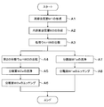
- FIG. 7 is a flow chart showing a main process of wafer processing.
- FIG. 8 is an explanatory diagram of a main process of wafer processing.
- the processing wafer W and the support wafer S are bonded to each other in an external bonding device (not shown) of the wafer processing system 1 to form a polymerized wafer T in advance.
- the cassette Ct containing a plurality of the polymerized wafers T shown in FIG. 8A is placed on the cassette mounting table 10 of the loading / unloading station 2.
- the polymerized wafer T in the cassette Ct is taken out by the wafer transfer device 22, and is transferred to the transition device 30.
- the wafer transfer device 42 takes out the polymerized wafer T of the transition device 30 and transfers it to the reformer 64.
- the peripheral reforming layer M1 is formed inside the processed wafer W as shown in FIG. 8 (b) (step A1 in FIG. 7), and further, the internal surface is modified as shown in FIG. 8 (c).
- a layer M2 is formed (step A2 in FIG. 7).
- the peripheral edge modification layer M1 serves as a base point when removing the peripheral edge portion We in the edge trim.
- the internal surface modification layer M2 serves as a base point for separating and thinning the processed wafer W.
- the polymerized wafer T is carried in from the wafer transfer device 42 and held by the chuck 100.
- the chuck 100 is moved to the macro alignment position.
- the macro alignment position is a position where the macro camera 120 can image the outer end portion of the processing wafer W.
- the macro camera 120 captures an image of the outer end portion of the processed wafer W at 360 degrees in the circumferential direction.
- the captured image is output from the macro camera 120 to the control device 70.
- the control device 70 calculates the first eccentricity of the center Cc of the chuck 100 and the center Cw of the processing wafer W from the image of the macro camera 120. Further, the control device 70 calculates the movement amount of the chuck 100 so as to correct the Y-axis component of the first eccentric amount based on the first eccentric amount.
- the chuck 100 moves in the Y-axis direction based on the calculated movement amount, and moves the chuck 100 to the micro-alignment position.
- the micro-alignment position is a position where the micro camera 121 can image the peripheral edge of the processing wafer W.
- the field of view of the micro camera 121 is as small as about 1/5 of that of the macro camera 120.
- the peripheral edge of the processing wafer W is the micro camera. It may not fit in the angle of view of 121 and cannot be imaged by the micro camera 121. Therefore, it can be said that the correction of the Y-axis component based on the first eccentricity amount is for moving the chuck 100 to the micro-alignment position.
- the boundary between the bonded region Aa and the unbonded region Ab at 360 degrees in the circumferential direction of the processed wafer W is imaged by the micro camera 121.
- the captured image is output from the micro camera 121 to the control device 70.
- the control device 70 calculates the second eccentric amount of the center Cc of the chuck 100 and the center Ca of the junction region Aa from the image of the micro camera 121. Further, the control device 70 determines the position of the chuck 100 with respect to the peripheral modification layer M1 so that the center of the junction region Aa and the center of the chuck 100 coincide with each other based on the second eccentricity amount.
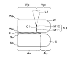
- laser light L1 (peripheral laser light L1) is irradiated from the laser head 110, and the peripheral modification layer M1 is formed at the boundary between the peripheral portion We and the central portion Wc of the processed wafer W.
- the peripheral modification layer M1 is formed radially inward with respect to the outer end portion of the bonding region Aa.
- step A1 the rotation mechanism 103 rotates the chuck 100 so that the center of the joining region Aa and the center of the chuck 100 coincide with the position of the chuck 100 determined by the control device 70, and the moving mechanism 104 rotates the chuck 100.
- the chuck 100 is moved in the Y-axis direction. At this time, the rotation of the chuck 100 and the movement in the Y-axis direction are synchronized.
- the laser beam L1 is irradiated from the laser head 110 to the inside of the processed wafer W. That is, the peripheral modification layer M1 is formed while correcting the second eccentricity amount. Then, the peripheral modification layer M1 is formed in an annular shape concentrically with the bonding region Aa. Therefore, after that, the peripheral edge portion We can be appropriately removed with the peripheral edge modification layer M1 as a base point.
- the chuck 100 when the second eccentricity amount includes the X-axis component, the chuck 100 is rotated while moving the chuck 100 in the Y-axis direction to correct the X-axis component.
- the second eccentricity amount when the second eccentricity amount does not include the X-axis component, it is sufficient to move the chuck 100 in the Y-axis direction without rotating it.
- step A1 as the peripheral edge modifying layer M1, two layers, for example, the lower peripheral edge modifying layer M11 and the upper peripheral edge modifying layer M12, are formed in the height direction (thickness direction) orthogonal to the surface direction of the processed wafer W. To do. Specifically, after forming the peripheral modification layer M11, the peripheral modification layer M12 is formed. For example, when the upper peripheral modification layer M12 is formed first and the laser light L1 is irradiated when the lower peripheral modification layer M11 is formed later, the laser light L1 is disturbed by the peripheral modification layer M12. There is a risk. Therefore, in the present embodiment, the lower peripheral modification layer M11 is formed first.
- the number of stages of the peripheral modification layer M1 is not limited to this, and may be one stage or three or more stages.
- cracks C1 are formed from each of the peripheral modification layer M11 and the peripheral modification layer M12.
- the crack C1 from the peripheral modification layer M11 extends downward and reaches the surface Wa.
- the crack C1 extending upward from the peripheral modification layer M11 and the crack C1 extending downward from the peripheral modification layer M12 are connected.
- the crack C1 does not extend upward from the peripheral modification layer M12.
- the crack C1 extending from the peripheral modification layer M11 is connected in the circumferential direction, and the crack C1 extending from the peripheral modification layer M12 is also connected in the circumferential direction.
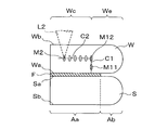
- the laser head 110 irradiates the laser beam L2 (inner surface laser beam L2) to form the internal surface modification layer M2 along the surface direction (FIG. 7).
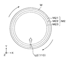
- Step A2 The black arrow shown in FIG. 12 indicates the rotation direction of the chuck 100.
- step A2 while rotating the chuck 100 (processed wafer W) once (360 degrees), the laser head 110 irradiates the inside of the processed wafer W with laser light L2 to form an annular internal surface modification layer M2. To do. After that, the laser head 110 is moved inward in the radial direction (Y-axis direction) of the processing wafer W. The formation of the annular inner surface modification layer M2 and the movement of the laser head 110 inward in the radial direction are repeatedly performed to form the inner surface modification layer M2 in the surface direction.
- the laser head 110 is moved in the Y-axis direction in forming the internal surface modification layer M2, but the chuck 100 may be moved in the Y-axis direction. Further, although the chuck 100 was rotated in forming the internal surface modification layer M2, the laser head 110 may be moved to rotate the laser head 110 relative to the chuck 100.
- step A2 as described above, a plurality of annular internal surface modification layers M2 are formed in the radial direction. That is, as shown in FIG. 13, the internal surface modification layer M2 has internal surface modification layers M21, M22, M23, M24, M25 and the like from the outer side to the inner side in the radial direction.
- the number of internal surface modification layers M2 in the radial direction is arbitrary.
- cracks C2 are formed from each of the plurality of internal surface modification layers M2.
- the crack C2 from the inner surface modification layer M21 extends radially outward and reaches the peripheral modification layer M12. Further, the crack C2 extending radially inward from the inner surface modified layer M21 and the crack C2 extending radially outward from the inner surface modified layer M22 are connected. In this way, the cracks C2 extending in the radial direction from the adjacent internal surface modification layers M2 and M2 are connected. The cracks C2 extending from each internal surface modification layer M2 are connected in the circumferential direction.
- the positional relationship between the peripheral modification layer M1 formed in step A1 and the internal surface modification layer M2 formed in step A2 will be described with reference to FIG.
- the internal surface modification layer M2 is formed inside the peripheral modification layer M1 in the radial direction. That is, the inner surface modification layer M21 is formed inside the peripheral modification layer M11 in the radial direction.
- the positional relationship in the height direction is determined by the position where the peripheral modification layer M1 is formed. ..
- the position of the upper end of the upper peripheral modification layer M12 is the same height as the position of the upper end of the inner surface modification layers M2 (M21 to M25) (dotted line in FIG. 13).
- the separation surfaces W1a and W2a (one-dot chain line portion of FIG. 13) of the processed wafer W are the central positions of the internal surface modification layer M2 in the height direction of the processed wafer W.
- the separation surface W2a is etched by the difference between the upper end of the peripheral modification layer M12 and the upper end of the inner surface modification layer M2.
- the peripheral modification layer M12 and the position of the upper end of the inner surface modification layer M2 are set to the same height as in the present embodiment, the peripheral modification layer M12 and the inner surface modification layer M2 The upper end of the can be set to the position to be etched, and the above-mentioned waste does not occur.
- the peripheral modification layer M1 (internal surface modification layer M2) spreads from the condensing position of the laser light L1 (laser light L2) depends on, for example, the energy, pulse width, and concentration correction of the laser light L1. It's decided.
- the pulse width indicates the irradiation time of one laser beam L1, and the larger the pulse width, the larger the peripheral modification layer M1.
- the degree of correction of the collection and dispersion is to correct whether the laser beam L1 is concentrated or diffused at one point, and if the laser beam L1 is diffused, the peripheral modification layer M1 also becomes large.
- the polymerized wafer T is carried out by the wafer transfer device 42.
- the polymerized wafer T is transferred to the separation device 63 by the wafer transfer device 42.
- the separation device 63 as shown in FIG. 8D, the processed wafer W is separated into the first separation wafer W1 and the second separation wafer W2 with the peripheral modification layer M1 and the inner surface modification layer M2 as base points. (Step A3 in FIG. 7). At this time, the peripheral portion We is also removed from the first separation wafer W1.
- step A3 as shown in FIG. 14A, of the polymerized wafer T, the suction plate 130 sucks and holds the processed wafer W, and the chuck 131 sucks and holds the support wafer S.
- a blade 132 having a wedge shape for example, is inserted at the interface between the processing wafer W and the support wafer S, and the first separation wafer W1 and the separation wafers W1a and W2a are defined as boundaries.
- the second separation wafer W2 is trimmed.
- FIG. 14 (c) in a state where the suction plate 130 sucks and holds the second separation wafer W2, the suction plate 130 is raised to lower the first separation wafer W1 to the second separation wafer W2. To separate.
- the pressure for sucking the second separation wafer W2 is measured by a pressure sensor (not shown) provided on the suction plate 130.
- a pressure sensor not shown
- the presence or absence of the second separation wafer W2 can be detected, and it can be confirmed whether or not the second separation wafer W2 has been separated from the first separation wafer W1.
- the method of separating the processed wafer W is not limited to this embodiment.
- the processing wafer W is separated only by raising the suction plate 130, but the processing wafer W may be separated by raising the suction plate 130 while rotating the suction plate 130.
- a tape (not shown) may be used instead of the suction plate 130, and the processed wafer W may be held and separated by the tape.
- ultrasonic waves may be applied to at least the internal surface modified layer M2 of the processed wafer W, or the internal surface modified layer M1 may be heated. May be good. In such a case, the processed wafer W can be easily separated from the internal surface modification layer M2 as a base point.
- the first separation wafer W1 and the second separation wafer W2 separated by the separation device 63 are subjected to separate processing.
- the second separated wafer W2 is transferred to the reversing device 61 by the wafer transfer device 42.
- the reversing device 61 the front and back surfaces of the second separation wafer W2 are reversed (step A4 in FIG. 7). That is, as shown in FIG. 8E, the separation surface W2a of the second separation wafer W2 is directed upward.
- the second separated wafer W2 is transferred to the cleaning device 62 by the wafer transfer device 42.
- the cleaning apparatus 62 as shown in FIG. 8E, the separation surface W2a of the second separation wafer W2 is scrubbed (step A5 in FIG. 7).
- step A5 while the second separation wafer W2 is rotationally held by the spin chuck (not shown), a scrub jig 140 such as a brush is brought into contact with the separation surface W2a from above, and the scrub jig 140 is brought into contact with the separation surface W2a.
- a scrub jig 140 such as a brush is brought into contact with the separation surface W2a from above, and the scrub jig 140 is brought into contact with the separation surface W2a.
- pure water is supplied from.
- the separation surface W2a is washed, and particles are removed from the separation surface W2a.
- the second separation wafer W2 is further rotated to spin-dry the separation surface W2a.
- the second separated wafer W2 is transferred to the etching device 60 by the wafer transfer device 42.
- the separation surface W2a of the second separation wafer W2 is wet-etched by the etching solution E (step A6 in FIG. 7).
- step A6 in a state where the second separation wafer W2 is rotationally held by the spin chuck (not shown), the etching solution is applied to the center of the separation surface W2a from the nozzle 150 arranged above the second separation wafer W2.
- Supply E The separation surface W2a is etched by this etching solution E, and the peripheral surface modification layer M1 and the internal surface modification layer M2 remaining on the separation surface W2a are removed. Further, since the peripheral modification layer M1 and the internal surface modification layer M2 remain in the scrub cleaning in step A5, particles may be generated again in this state, but the etching in this step A6 causes the particles to be generated again. Particles are also removed.
- the amount of etching of the separation surface W2a should be minimized. Can be done. Therefore, the consumption of the etching solution E can be suppressed and the time required for etching can be shortened.
- the peripheral portion W2e remains on the second separation wafer W2. Since the etching solution E is supplied from above in this state, the etching solution E is stored in the space surrounded by the peripheral portion W2e and a paddle is formed. Therefore, the consumption of the etching solution E can be further suppressed.
- step A6 after etching the separation surface W2a in this way, the supply of the etching solution E from the nozzle 150 is stopped, the separation surface W2a is further washed with pure water, and then the second separation wafer W2 is transferred. Further rotation is performed to spin dry the separation surface W2a.
- the second separated wafer W2 that has been subjected to all the processing is transferred to the cassette Cw2 of the cassette mounting table 10 by the wafer transfer device 22.
- the desired processing is performed on the first separation wafer W1.
- the first separated wafer W1 separated by the separation device 63 is transferred to the cleaning device 62 by the wafer transfer device 42.
- the cleaning device 62 as shown in FIG. 8 (g), the separation surface W1a of the first separation wafer W1 is scrubbed (step A7 in FIG. 7).
- step A7 as in step A5, pure water is supplied with the scrub jig 140 in contact with the separation surface W1a from above, and the separation surface W1a is washed.
- the first separated wafer W1 is transferred to the etching device 60 by the wafer transfer device 42.
- the separation surface W1a of the first separation wafer W1 is wet-etched by the etching solution E (step A8 in FIG. 7).
- the peripheral modification layer M1 and the internal modification layer M2 remaining on the separation surface W1a are removed.
- the separation surface W1a is etched so that the first separation wafer W1 is thinned to a desired thickness.
- the first separated wafer W1 that has been subjected to all the processing is transferred to the cassette Cw1 of the cassette mounting table 10 by the wafer transfer device 22.
- the first separation wafer W1 may be conveyed to the cassette Ct. In this way, a series of wafer processing in the wafer processing system 1 is completed.
- the separation surface W2a side is ground and the peripheral edge portion W2e is removed. Then, the separation surface W2a is washed and particles are removed from the ground second separation wafer W2, and then the separation surface W2a is further etched to remove grinding marks. Then, when the second separation wafer W2 is reused as, for example, a product wafer, the separation surface W2a is further polished (CMP). On the other hand, when the second separation wafer W2 is reused as a support wafer for supporting the product wafer, for example, it is used as it is.
- the separation surface W1a is polished (CMP).
- CMP polishing the separation surface W1a since the first separation wafer W1 is etched to a desired thickness in step A8 as described above, it is only necessary to polish the separation surface W1a. However, for example, when the first separation wafer W1 does not have a desired thickness in step A8, the separation surface W1a is ground to a desired thickness outside the wafer processing system 1. After that, the separated surface W1a is cleaned, the separated surface W1a is etched, and the separated surface W1a is polished on the ground first separated wafer W1.
- steps A1 to A8 can be performed to separate the processed wafers W, and the separation surfaces W1a and W2a of the separated wafers W1 and W2 can be appropriately processed by cleaning, etching or the like, respectively. Therefore, the first separation wafer W1 having the device layer can be commercialized, and the second separation wafer W2 can be reused. Moreover, since these steps A1 to A8 are performed by one wafer processing system 1, the wafer processing can be efficiently performed.
- steps A1 and A2 may be exchanged to form the internal surface modification layer M2, and then the peripheral modification layer M1 may be formed.
- the laser beam L1 may be disturbed by the inner surface modification layer M2 when forming the peripheral modification layer M1, particularly the lower peripheral modification layer M11, step A1 as in the present embodiment. It is preferable to form the inner surface modified layer M2 in step A2 after forming the peripheral modified layer M1 in step A2.
- the peripheral edge modification is performed so that the position of the upper end of the upper peripheral modification layer M12 is the same as the position of the upper end of the inner surface modification layer M2.
- a layer M1 and an internal surface modification layer M2 are formed.
- the edges of the peripheral surface modification layer M12 and the inner surface modification layer M2 may be etched to minimize the etching amount. Can be done. Therefore, the consumption of the etching solution E can be suppressed and the time required for etching can be shortened.
- the position of the upper end of the uppermost peripheral modification layer M1 is at the same height as the position of the upper end of the inner surface modification layer M2. It should be. Even in such a case, the same effect as described above can be enjoyed.
- the peripheral surface modification layer M12 and the internal surface modification If the layers M2 are formed at the same height, they can be reused as a product wafer. That is, even if the second separated wafer W2 after being separated with the separation surface W2a as a boundary is further etched, ground, CMP, or the like, a thickness of about 700 ⁇ m remains. In such a case, a device can be formed on the surface of the second separation wafer W2 and commercialized.
- the peripheral surface modified layer M12 and the internal surface modified layer M2 have the same height.
- it can be reused as a support wafer that supports the product wafer. That is, even if the second separated wafer W2 after being separated with the separation surface W2a as a boundary is further etched, ground, or the like, a thickness of about 600 ⁇ m remains.
- the second separation wafer W2 can be used as a support wafer for supporting the product wafer in the temporary bonding process when the product wafer is thinned.
- the second separation wafer W2 can also be reused as a product wafer having a device region in which a plurality of devices are formed on the surface and an outer peripheral surplus region surrounding the device region.
- the separation surface W2a may not be ground with respect to the second separation wafer W2 processed by the wafer processing system 1, and the peripheral edge portion W2e may be left.
- 15 to 21 are explanatory views showing the positional relationship between the peripheral modification layer M1 and the internal surface modification layer M2 according to the other embodiments, respectively.
- the radial positional relationship between the peripheral modification layer M1 and the internal surface modification layer M2 shown in FIGS. 15 to 17 is the same as the positional relationship shown in FIG. That is, the inner surface modification layer M2 (inner surface modification layer M21) is formed radially inside the peripheral modification layer M1 (peripheral modification layer M12).
- the position of the upper end of the inner surface modification layer M2 is higher than the position of the upper end of the peripheral modification layer M12. Further, the position of the upper end of the inner surface modification layer M2 is the same height as the position of the apex of the crack C1 extending upward from the upper end of the peripheral modification layer M12.
- the position of the upper end of the inner surface modification layer M2 is the same as the position of the upper end of the peripheral modification layer M12. Is. However, the crack C1 extends slightly upward from the upper end of the peripheral modification layer M12.
- the position of the upper end of the inner surface modification layer M2 is higher than the position of the upper end of the peripheral modification layer M12. Further, the position of the upper end of the internal surface modification layer M2 is higher than the position of the apex of the crack C1 extending upward from the upper end of the peripheral modification layer M12, and the crack C1 and the crack C2 are connected.
- the end portion of the internal surface modification layer M2 may be etched to minimize the etching amount. It can be suppressed to the limit. Therefore, the consumption of the etching solution E can be suppressed and the time required for etching can be shortened.
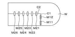
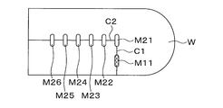
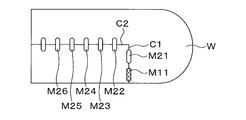
- the radial positional relationship between the peripheral modification layer M1 and the internal surface modification layer M2 shown in FIGS. 18 to 21 is the same as the positional relationship shown in FIGS. 13 and 15 to 17. That is, the outermost inner surface modified layer M21 is formed at the same position in the radial direction as the peripheral modified layer M11 and above the peripheral modified layer M11.
- the position of the upper end of the outermost inner surface modification layer M21 is the position of the inner surface modification layer M22. It is the same height as the position of the upper end, and is naturally higher than the position of the peripheral modification layer M11. Further, the inner surface modification layers M22 to M26 and the like on the inner side in the radial direction of the inner surface modification layer M21 are formed at the same height. Further, the crack C1 extending upward from the upper end of the peripheral modification layer M11 extends to the inner surface modification layer M21.
- the position of the upper end of the outermost inner surface modification layer M21 is the position of the inner inner surface modification layer M22. It is lower than the position of the upper end and naturally higher than the position of the peripheral modification layer M11. Further, the inner surface modification layers M22 to M26 and the like on the inner side in the radial direction of the inner surface modification layer M21 are formed at the same height. Further, the position of the apex of the crack C1 extending upward from the upper end of the peripheral modification layer M11 is the same height as the position of the upper end of the inner surface modification layers M22 to M26 and the like.
- the position of the upper end of the outermost inner surface modification layer M21 is the position of the inner inner surface modification layer M22. It is the same height as the position of the upper end, and is naturally higher than the position of the peripheral modification layer M11. Further, the inner surface modification layers M22 to M26 and the like on the inner side in the radial direction of the inner surface modification layer M21 are formed at the same height. Further, the crack C1 extending upward from the upper end of the peripheral modification layer M11 extends slightly above the position of the upper end of the inner surface modification layers M22 to M26 and the like.
- the position of the upper end of the outermost inner surface modification layer M21 is the position of the inner inner surface modification layer M22. It is lower than the position of the upper end and naturally higher than the position of the peripheral modification layer M11. Further, the inner surface modification layers M22 to M26 and the like on the inner side in the radial direction of the inner surface modification layer M21 are formed at the same height. Further, the position of the apex of the crack C1 extending upward from the upper end of the peripheral modification layer M11 is lower than the position of the upper end of the inner surface modification layers M22 to M26, and the crack C1 and the crack C2 are connected.
- the inner surface modified layer M2 is formed after forming the peripheral modified layer M11.
- the inner surface modification layer M2 is formed first, if the laser light L1 is irradiated when the peripheral surface modification layer M11 is formed later, the laser light L1 may be disturbed by the inner surface modification layer M2. is there. Therefore, in the present embodiment, the internal surface modification layer M2 is formed first.
- the separation surfaces W1a and W2a are formed on the internal surface modification layer M2 in the height direction of the processing wafer W. Although it was at the center position, it may be the upper end of the internal surface modification layer M2 or the lower end.
- the etching solution E is supplied from above to the separation surface W2a of the second separation wafer W2, but the wafer processing system 1 supplies the etching solution E from below the separation surface W2a. You may have more devices.
- Such an etching apparatus is provided, for example, by being laminated with the etching apparatus 60.
- the wafer processing system 1 may further have a cleaning device for cleaning from below the separation surface W2a. Good.
- a cleaning device is provided, for example, in a laminated manner with the cleaning device 62.
- FIG. 22 is an explanatory diagram of a main process of wafer processing performed by the wafer processing system 1.
- the processed wafers W are separated by performing steps A1 to A3 as shown in FIGS. 22 (a) to 22 (d) as in the above embodiment.
- steps A1 to A3 as shown in FIGS. 22 (a) to 22 (d) as in the above embodiment.
- step A4 is omitted.
- the reversing device 61 may be omitted from the wafer processing system 1.
- step A5 the separated second separation wafer W2 is conveyed to the cleaning apparatus.
- a scrub jig 200 such as a brush is applied to the separation surface W2a from below while the second separation wafer W2 is rotationally held by a chuck (not shown) as shown in FIG. 22 (e).
- pure water is supplied from the scrub jig 200 while being in contact with the scrub jig 200.
- the separation surface W2a is washed.
- step A6 the second separation wafer W2 is conveyed to the etching apparatus.
- the second separation wafer W2 is rotationally held by the chuck (not shown) from the nozzle 210 arranged below the second separation wafer W2.
- the etching solution E is supplied to the central portion of the separation surface W2a.
- the separation surface W2a is etched by this etching solution E.
- steps A7 are performed on the first separation wafer W1 as shown in FIGS. 22 (g) to 22 (h).
- -A8 is performed, and the separation surface W1a is washed and etched.
- the wafer processing system 1 may further have a grinding device 220 as a grinding unit in the configuration of the above embodiment.
- the separation surface W2a (including the peripheral edge portion W2e) of the second separation wafer W2 is ground outside the wafer processing system 1, but in the present embodiment, the separation surface W2a is ground by the grinding device 220.
- the separation surface W1a of the first separation wafer W1 is also ground by the grinding apparatus 220 will be described.
- the grinding device 220 has a rotary table 230, a first grinding unit 240, and a second grinding unit 250.
- the rotary table 230 is rotatably configured around a vertical rotation center line 231 by a rotation mechanism (not shown).
- a rotation mechanism (not shown).
- the chucks 232 are arranged evenly on the same circumference as the rotary table 230, that is, every 90 degrees.
- the four chucks 232 can be moved to the delivery position A0 and the processing positions A1 and A2 by rotating the rotary table 230.
- the chuck 232 is configured to be rotatable by a rotation mechanism (not shown).
- the delivery position A0 is the position on the wafer transfer region 40 side (X-axis negative direction side and Y-axis positive direction side) of the rotary table 230, and the separated wafers W1 and W2 are delivered.
- the first machining position A1 is a position on the X-axis positive direction side and the Y-axis positive direction side of the rotary table 230, and the first grinding unit 240 is arranged.
- the second machining position A2 is a position on the X-axis negative direction side and the Y-axis negative direction side of the rotary table 230, and the second grinding unit 250 is arranged.
- the first grinding unit 240 grinds the separation surface W1a of the first separation wafer W1.
- the first grinding unit 240 has a first grinding unit 241 provided with an annularly shaped and rotatable grinding wheel (not shown). Further, the first grinding portion 241 is configured to be movable in the vertical direction along the support column 242. Then, in a state where the separation surface W1a of the first separation wafer W1 held by the chuck 232 is in contact with the grinding wheel, the chuck 232 and the grinding wheel are each rotated to grind the separation surface W1a.
- the second grinding unit 250 grinds the separation surface W2a of the second separation wafer W2.
- the second grinding unit 250 has a second grinding unit 251 provided with an annularly shaped and rotatable grinding wheel (not shown). Further, the second grinding portion 251 is configured to be movable in the vertical direction along the support column 252. Then, in a state where the separation surface W2a of the second separation wafer W2 held by the chuck 232 is in contact with the grinding wheel, the chuck 232 and the grinding wheel are each rotated to grind the separation surface W2a.
- FIG. 24 is an explanatory diagram of a main process of wafer processing performed by the wafer processing system 1.
- FIG. 24 illustrates the processing of the separated wafers W1 and W2 after performing steps A1 to A8 shown in FIGS. 8A to 8H of the above embodiment. That is, FIGS. 24A to 24C show the processing performed on the second separation wafer W2 in which the separation surface W2a is etched as shown in FIG. 8F. Further, FIGS. 24 (d) to 24 (f) show the processing performed on the first separation wafer W1 in which the separation surface W1a is etched as shown in FIG. 8 (h).
- the second separated wafer W2 etched by the etching apparatus 60 as shown in FIG. 8F is conveyed to the grinding apparatus 220 by the wafer conveying apparatus 42.
- the second separation wafer W2 is delivered to the chuck 232 at the delivery position A0.
- the rotary table 230 is rotated to move the second separation wafer W2 to the second processing position A2.
- the separation surface W2a is ground using the second grinding portion 251 to remove the peripheral edge portion W2e.
- the rotary table 230 is rotated to move the second separation wafer W2 to the delivery position A0.
- the separation surface W2a may be cleaned with a cleaning liquid.
- the second separated wafer W2 is transferred to the cleaning device 62 by the wafer transfer device 42.
- the cleaning device 62 the separation surface W2a of the second separation wafer W2 is scrubbed using the scrub jig 140 as shown in FIG. 24 (b). Then, the particles on the separation surface W2a are removed.
- the second separated wafer W2 is transferred to the etching device 60 by the wafer transfer device 42.
- the etching solution E is supplied from the nozzle 150 arranged above the second separation wafer W2 to the separation surface W2a, and the separation surface W2a is etched. Then, the grinding marks remaining on the separation surface W2a are removed.
- the desired processing is performed on the first separation wafer W1. ..
- the first separated wafer W1 etched by the etching apparatus 60 is conveyed to the grinding apparatus 220 by the wafer conveying apparatus 42.
- the first separation wafer W1 is delivered to the chuck 232 at the delivery position A0.
- the rotary table 230 is rotated to move the first separation wafer W1 to the first processing position A1.
- the separation surface W1a is ground using the first grinding unit 241 to thin the first separation wafer W1 to a desired thickness.
- the rotary table 230 is rotated to move the first separation wafer W1 to the delivery position A0. At this time, the separation surface W1a may be cleaned with a cleaning liquid.
- the first separated wafer W1 is transferred to the cleaning device 62 by the wafer transfer device 42.
- the cleaning device 62 the separation surface W1a of the first separation wafer W1 is scrubbed using the scrub jig 140 as shown in FIG. 24 (e). Then, the particles on the separation surface W1a are removed.
- the first separated wafer W1 is transferred to the etching device 60 by the wafer transfer device 42.
- the etching solution E is supplied to the separation surface W1a from the nozzle 150 arranged above the first separation wafer W1, and the separation surface W1a is etched. Then, the grinding marks remaining on the separation surface W1a are removed.
- the separation surface W2a is polished outside the wafer processing system 1. Further, the separation surface W1a of the first separation wafer W1 processed as described above is polished outside the wafer processing system 1.
- the wafer processing system 1 has the grinding device 220, it is possible to grind the separation surfaces W1a and W2a, and the throughput of wafer processing can be further improved.
- the grinding of the separation surface W1a shown in FIG. 24D is omitted, and further, FIG. Cleaning of the separation surface W1a shown in 24 (e) and etching of the separation surface W1a shown in FIG. 24 (f) may be omitted.
- a plurality of annular internal surface modification layers M2 are formed in step A2, but the internal surface modification layers M2 may be spirally formed from the outer side in the radial direction to the inner side.
- the inside of the processed wafer W is moved from the laser head 110. Is irradiated with the laser beam L2.
- the processed wafer W and the support wafer S are directly bonded has been described, but the processed wafer W and the support wafer S may be bonded via an adhesive.
- the above embodiment the case where the processed wafer W in the polymerization wafer T is thinned has been described, but the above embodiment can also be applied to the case where one wafer is thinned.
- one wafer may be thinned and then bonded to the support wafer S to form a polymerized wafer T.
- the processing wafer W as the processing object is a silicon wafer
- the type of the processing object is not limited to this.
- a glass substrate, a SiC substrate, a sapphire substrate, a single crystal substrate, a polycrystalline substrate, an amorphous substrate, or the like may be selected instead of the silicon wafer.
- an ingot, a base, a thin plate, or the like may be selected instead of the substrate.
- the shape of the processed wafer W is circular has been described as an example, but the shape of the processed wafer W is not limited to this, for example, a square shape (square shape) or the like. Can take any shape of.
- the technique according to the present disclosure can be applied when producing a processed wafer W having a device region in which a plurality of devices are formed on the surface and an outer peripheral surplus region surrounding the device region. it can.
Landscapes
- Engineering & Computer Science (AREA)
- Physics & Mathematics (AREA)
- Optics & Photonics (AREA)
- Chemical Kinetics & Catalysis (AREA)
- General Chemical & Material Sciences (AREA)
- Oil, Petroleum & Natural Gas (AREA)
- Chemical & Material Sciences (AREA)
- Plasma & Fusion (AREA)
- Mechanical Engineering (AREA)
- Mechanical Treatment Of Semiconductor (AREA)
- Cleaning Or Drying Semiconductors (AREA)
- Laser Beam Processing (AREA)
- Weting (AREA)
- Container, Conveyance, Adherence, Positioning, Of Wafer (AREA)
Priority Applications (1)
| Application Number | Priority Date | Filing Date | Title |
|---|---|---|---|
| JP2021514898A JP7129558B2 (ja) | 2019-04-19 | 2020-04-07 | 処理装置及び処理方法 |
Applications Claiming Priority (2)
| Application Number | Priority Date | Filing Date | Title |
|---|---|---|---|
| JP2019-080300 | 2019-04-19 | ||
| JP2019080300 | 2019-04-19 |
Publications (1)
| Publication Number | Publication Date |
|---|---|
| WO2020213479A1 true WO2020213479A1 (ja) | 2020-10-22 |
Family
ID=72837833
Family Applications (1)
| Application Number | Title | Priority Date | Filing Date |
|---|---|---|---|
| PCT/JP2020/015687 Ceased WO2020213479A1 (ja) | 2019-04-19 | 2020-04-07 | 処理装置及び処理方法 |
Country Status (3)
| Country | Link |
|---|---|
| JP (1) | JP7129558B2 (https=) |
| TW (1) | TWI858047B (https=) |
| WO (1) | WO2020213479A1 (https=) |
Cited By (5)
| Publication number | Priority date | Publication date | Assignee | Title |
|---|---|---|---|---|
| JPWO2022190908A1 (https=) * | 2021-03-09 | 2022-09-15 | ||
| JPWO2022190924A1 (https=) * | 2021-03-12 | 2022-09-15 | ||
| JP2023026825A (ja) * | 2021-08-16 | 2023-03-01 | 株式会社ディスコ | ウエーハの加工方法 |
| JPWO2023238542A1 (https=) * | 2022-06-07 | 2023-12-14 | ||
| WO2025204976A1 (ja) * | 2024-03-27 | 2025-10-02 | 東京エレクトロン株式会社 | 基板処理方法及び基板処理システム |
Families Citing this family (1)
| Publication number | Priority date | Publication date | Assignee | Title |
|---|---|---|---|---|
| US20240067555A1 (en) * | 2022-08-22 | 2024-02-29 | Uti Inc. | Method of manufacturing sapphire cover window and sapphire cover window manufactured thereby |
Citations (8)
| Publication number | Priority date | Publication date | Assignee | Title |
|---|---|---|---|---|
| JP2011155069A (ja) * | 2010-01-26 | 2011-08-11 | Saitama Univ | 基板加工方法 |
| WO2012014716A1 (ja) * | 2010-07-26 | 2012-02-02 | 浜松ホトニクス株式会社 | チップの製造方法 |
| JP2015138951A (ja) * | 2014-01-24 | 2015-07-30 | 株式会社ディスコ | ウェーハの加工方法 |
| JP2015204442A (ja) * | 2014-04-16 | 2015-11-16 | 信越ポリマー株式会社 | 原盤製造方法及び原盤 |
| JP2017071074A (ja) * | 2015-10-05 | 2017-04-13 | 国立大学法人埼玉大学 | 内部加工層形成単結晶基板の製造方法、および、単結晶基板の製造方法 |
| JP2017195244A (ja) * | 2016-04-19 | 2017-10-26 | 株式会社ディスコ | SiCウエーハの加工方法 |
| JP2017195245A (ja) * | 2016-04-19 | 2017-10-26 | 株式会社ディスコ | SiCウエーハの加工方法 |
| JP2020069533A (ja) * | 2018-10-30 | 2020-05-07 | 浜松ホトニクス株式会社 | レーザ加工装置及びレーザ加工方法 |
Family Cites Families (9)
| Publication number | Priority date | Publication date | Assignee | Title |
|---|---|---|---|---|
| WO2009007003A1 (en) * | 2007-07-11 | 2009-01-15 | S.O.I. Tec Silicon On Insulator Technologies | Method for recycling a substrate, laminated water fabricating method and suitable recycled donor substrate |
| JP5093850B2 (ja) * | 2008-06-26 | 2012-12-12 | リンテック株式会社 | シート剥離装置及び剥離方法 |
| JP2010021398A (ja) * | 2008-07-11 | 2010-01-28 | Disco Abrasive Syst Ltd | ウェーハの処理方法 |
| US9214353B2 (en) | 2012-02-26 | 2015-12-15 | Solexel, Inc. | Systems and methods for laser splitting and device layer transfer |
| KR101803790B1 (ko) * | 2013-04-18 | 2017-12-04 | 한화테크윈 주식회사 | 웨이퍼의 시닝 방법 및 장치 |
| JP2015032690A (ja) | 2013-08-02 | 2015-02-16 | 株式会社ディスコ | 積層ウェーハの加工方法 |
| JP6552898B2 (ja) | 2015-07-13 | 2019-07-31 | 株式会社ディスコ | 多結晶SiCウエーハの生成方法 |
| US10978311B2 (en) | 2016-12-12 | 2021-04-13 | Siltectra Gmbh | Method for thinning solid body layers provided with components |
| CN110785833A (zh) | 2017-06-19 | 2020-02-11 | 罗姆股份有限公司 | 半导体装置的制造方法及晶片粘合结构体 |
-
2020
- 2020-04-07 WO PCT/JP2020/015687 patent/WO2020213479A1/ja not_active Ceased
- 2020-04-07 JP JP2021514898A patent/JP7129558B2/ja active Active
- 2020-04-09 TW TW109111892A patent/TWI858047B/zh active
Patent Citations (8)
| Publication number | Priority date | Publication date | Assignee | Title |
|---|---|---|---|---|
| JP2011155069A (ja) * | 2010-01-26 | 2011-08-11 | Saitama Univ | 基板加工方法 |
| WO2012014716A1 (ja) * | 2010-07-26 | 2012-02-02 | 浜松ホトニクス株式会社 | チップの製造方法 |
| JP2015138951A (ja) * | 2014-01-24 | 2015-07-30 | 株式会社ディスコ | ウェーハの加工方法 |
| JP2015204442A (ja) * | 2014-04-16 | 2015-11-16 | 信越ポリマー株式会社 | 原盤製造方法及び原盤 |
| JP2017071074A (ja) * | 2015-10-05 | 2017-04-13 | 国立大学法人埼玉大学 | 内部加工層形成単結晶基板の製造方法、および、単結晶基板の製造方法 |
| JP2017195244A (ja) * | 2016-04-19 | 2017-10-26 | 株式会社ディスコ | SiCウエーハの加工方法 |
| JP2017195245A (ja) * | 2016-04-19 | 2017-10-26 | 株式会社ディスコ | SiCウエーハの加工方法 |
| JP2020069533A (ja) * | 2018-10-30 | 2020-05-07 | 浜松ホトニクス株式会社 | レーザ加工装置及びレーザ加工方法 |
Cited By (12)
| Publication number | Priority date | Publication date | Assignee | Title |
|---|---|---|---|---|
| JPWO2022190908A1 (https=) * | 2021-03-09 | 2022-09-15 | ||
| WO2022190908A1 (ja) * | 2021-03-09 | 2022-09-15 | 東京エレクトロン株式会社 | 積層基板の製造方法、及び基板処理装置 |
| JP7643816B2 (ja) | 2021-03-09 | 2025-03-11 | 東京エレクトロン株式会社 | 積層基板の製造方法 |
| JPWO2022190924A1 (https=) * | 2021-03-12 | 2022-09-15 | ||
| WO2022190924A1 (ja) * | 2021-03-12 | 2022-09-15 | 東京エレクトロン株式会社 | 基板処理装置、基板処理システム及び基板処理方法 |
| JP7546754B2 (ja) | 2021-03-12 | 2024-09-06 | 東京エレクトロン株式会社 | 基板処理装置、基板処理システム及び基板処理方法 |
| JP2023026825A (ja) * | 2021-08-16 | 2023-03-01 | 株式会社ディスコ | ウエーハの加工方法 |
| JP7772523B2 (ja) | 2021-08-16 | 2025-11-18 | 株式会社ディスコ | ウエーハの加工方法 |
| JPWO2023238542A1 (https=) * | 2022-06-07 | 2023-12-14 | ||
| WO2023238542A1 (ja) * | 2022-06-07 | 2023-12-14 | 東京エレクトロン株式会社 | 基板処理システム及び基板処理方法 |
| JP7806234B2 (ja) | 2022-06-07 | 2026-01-26 | 東京エレクトロン株式会社 | 基板処理システム及び基板処理方法 |
| WO2025204976A1 (ja) * | 2024-03-27 | 2025-10-02 | 東京エレクトロン株式会社 | 基板処理方法及び基板処理システム |
Also Published As
| Publication number | Publication date |
|---|---|
| JPWO2020213479A1 (https=) | 2020-10-22 |
| JP7129558B2 (ja) | 2022-09-01 |
| TW202046391A (zh) | 2020-12-16 |
| TWI858047B (zh) | 2024-10-11 |
Similar Documents
| Publication | Publication Date | Title |
|---|---|---|
| JP7129558B2 (ja) | 処理装置及び処理方法 | |
| JP7093855B2 (ja) | 基板処理装置及び基板処理方法 | |
| KR102839396B1 (ko) | 처리 장치 및 처리 방법 | |
| JP7086201B2 (ja) | 基板処理システム及び基板処理方法 | |
| JPWO2020129732A1 (ja) | 基板処理装置及び基板処理方法 | |
| CN114096372B (zh) | 处理装置和处理方法 | |
| JPWO2020129730A1 (ja) | 基板処理装置及び基板処理方法 | |
| CN113195152B (zh) | 基板处理装置和基板处理方法 | |
| JPWO2020184179A1 (ja) | 基板処理装置及び基板処理方法 | |
| JP7170879B2 (ja) | 処理装置及び処理方法 | |
| JP7170880B2 (ja) | 処理装置及び処理方法 | |
| CN114096374B (zh) | 处理装置和处理方法 | |
| TWI832975B (zh) | 處理裝置及處理方法 | |
| JP2021019056A (ja) | 処理装置及び処理方法 | |
| JP7633882B2 (ja) | 処理システム及び処理方法 |
Legal Events
| Date | Code | Title | Description |
|---|---|---|---|
| 121 | Ep: the epo has been informed by wipo that ep was designated in this application |
Ref document number: 20791219 Country of ref document: EP Kind code of ref document: A1 |
|
| ENP | Entry into the national phase |
Ref document number: 2021514898 Country of ref document: JP Kind code of ref document: A |
|
| NENP | Non-entry into the national phase |
Ref country code: DE |
|
| 122 | Ep: pct application non-entry in european phase |
Ref document number: 20791219 Country of ref document: EP Kind code of ref document: A1 |