WO2022190924A1 - 基板処理装置、基板処理システム及び基板処理方法 - Google Patents
基板処理装置、基板処理システム及び基板処理方法 Download PDFInfo
- Publication number
- WO2022190924A1 WO2022190924A1 PCT/JP2022/008206 JP2022008206W WO2022190924A1 WO 2022190924 A1 WO2022190924 A1 WO 2022190924A1 JP 2022008206 W JP2022008206 W JP 2022008206W WO 2022190924 A1 WO2022190924 A1 WO 2022190924A1
- Authority
- WO
- WIPO (PCT)
- Prior art keywords
- substrate
- laser
- wafer
- laser oscillator
- processing apparatus
- Prior art date
Links
- 239000000758 substrate Substances 0.000 title claims abstract description 102
- 238000003672 processing method Methods 0.000 title claims description 5
- 230000003287 optical effect Effects 0.000 claims abstract description 55
- 230000001678 irradiating effect Effects 0.000 claims description 13
- 239000012212 insulator Substances 0.000 claims description 5
- 238000000034 method Methods 0.000 abstract description 6
- 235000012431 wafers Nutrition 0.000 description 201
- 238000010521 absorption reaction Methods 0.000 description 17
- 238000004140 cleaning Methods 0.000 description 13
- 238000012423 maintenance Methods 0.000 description 8
- 230000007704 transition Effects 0.000 description 7
- 239000004065 semiconductor Substances 0.000 description 4
- 230000005540 biological transmission Effects 0.000 description 3
- 238000003860 storage Methods 0.000 description 3
- 229910004298 SiO 2 Inorganic materials 0.000 description 2
- XUIMIQQOPSSXEZ-UHFFFAOYSA-N Silicon Chemical compound [Si] XUIMIQQOPSSXEZ-UHFFFAOYSA-N 0.000 description 2
- 238000009434 installation Methods 0.000 description 2
- 229910052710 silicon Inorganic materials 0.000 description 2
- 239000010703 silicon Substances 0.000 description 2
- BOTDANWDWHJENH-UHFFFAOYSA-N Tetraethyl orthosilicate Chemical compound CCO[Si](OCC)(OCC)OCC BOTDANWDWHJENH-UHFFFAOYSA-N 0.000 description 1
- 239000000853 adhesive Substances 0.000 description 1
- 230000001070 adhesive effect Effects 0.000 description 1
- 239000000498 cooling water Substances 0.000 description 1
- 230000032798 delamination Effects 0.000 description 1
- 238000010586 diagram Methods 0.000 description 1
- 238000006073 displacement reaction Methods 0.000 description 1
- 230000000694 effects Effects 0.000 description 1
- 238000004519 manufacturing process Methods 0.000 description 1
- 238000000926 separation method Methods 0.000 description 1
Images


Classifications
-
- B—PERFORMING OPERATIONS; TRANSPORTING
- B23—MACHINE TOOLS; METAL-WORKING NOT OTHERWISE PROVIDED FOR
- B23K—SOLDERING OR UNSOLDERING; WELDING; CLADDING OR PLATING BY SOLDERING OR WELDING; CUTTING BY APPLYING HEAT LOCALLY, e.g. FLAME CUTTING; WORKING BY LASER BEAM
- B23K26/00—Working by laser beam, e.g. welding, cutting or boring
- B23K26/02—Positioning or observing the workpiece, e.g. with respect to the point of impact; Aligning, aiming or focusing the laser beam
- B23K26/06—Shaping the laser beam, e.g. by masks or multi-focusing
- B23K26/064—Shaping the laser beam, e.g. by masks or multi-focusing by means of optical elements, e.g. lenses, mirrors or prisms
- B23K26/0648—Shaping the laser beam, e.g. by masks or multi-focusing by means of optical elements, e.g. lenses, mirrors or prisms comprising lenses
-
- B—PERFORMING OPERATIONS; TRANSPORTING
- B23—MACHINE TOOLS; METAL-WORKING NOT OTHERWISE PROVIDED FOR
- B23K—SOLDERING OR UNSOLDERING; WELDING; CLADDING OR PLATING BY SOLDERING OR WELDING; CUTTING BY APPLYING HEAT LOCALLY, e.g. FLAME CUTTING; WORKING BY LASER BEAM
- B23K26/00—Working by laser beam, e.g. welding, cutting or boring
- B23K26/02—Positioning or observing the workpiece, e.g. with respect to the point of impact; Aligning, aiming or focusing the laser beam
- B23K26/06—Shaping the laser beam, e.g. by masks or multi-focusing
- B23K26/064—Shaping the laser beam, e.g. by masks or multi-focusing by means of optical elements, e.g. lenses, mirrors or prisms
- B23K26/0643—Shaping the laser beam, e.g. by masks or multi-focusing by means of optical elements, e.g. lenses, mirrors or prisms comprising mirrors
-
- B—PERFORMING OPERATIONS; TRANSPORTING
- B23—MACHINE TOOLS; METAL-WORKING NOT OTHERWISE PROVIDED FOR
- B23K—SOLDERING OR UNSOLDERING; WELDING; CLADDING OR PLATING BY SOLDERING OR WELDING; CUTTING BY APPLYING HEAT LOCALLY, e.g. FLAME CUTTING; WORKING BY LASER BEAM
- B23K26/00—Working by laser beam, e.g. welding, cutting or boring
- B23K26/50—Working by transmitting the laser beam through or within the workpiece
- B23K26/57—Working by transmitting the laser beam through or within the workpiece the laser beam entering a face of the workpiece from which it is transmitted through the workpiece material to work on a different workpiece face, e.g. for effecting removal, fusion splicing, modifying or reforming
-
- H—ELECTRICITY
- H01—ELECTRIC ELEMENTS
- H01L—SEMICONDUCTOR DEVICES NOT COVERED BY CLASS H10
- H01L21/00—Processes or apparatus adapted for the manufacture or treatment of semiconductor or solid state devices or of parts thereof
- H01L21/02—Manufacture or treatment of semiconductor devices or of parts thereof
- H01L21/04—Manufacture or treatment of semiconductor devices or of parts thereof the devices having at least one potential-jump barrier or surface barrier, e.g. PN junction, depletion layer or carrier concentration layer
- H01L21/18—Manufacture or treatment of semiconductor devices or of parts thereof the devices having at least one potential-jump barrier or surface barrier, e.g. PN junction, depletion layer or carrier concentration layer the devices having semiconductor bodies comprising elements of Group IV of the Periodic System or AIIIBV compounds with or without impurities, e.g. doping materials
- H01L21/30—Treatment of semiconductor bodies using processes or apparatus not provided for in groups H01L21/20 - H01L21/26
- H01L21/302—Treatment of semiconductor bodies using processes or apparatus not provided for in groups H01L21/20 - H01L21/26 to change their surface-physical characteristics or shape, e.g. etching, polishing, cutting
- H01L21/304—Mechanical treatment, e.g. grinding, polishing, cutting
-
- H—ELECTRICITY
- H01—ELECTRIC ELEMENTS
- H01L—SEMICONDUCTOR DEVICES NOT COVERED BY CLASS H10
- H01L21/00—Processes or apparatus adapted for the manufacture or treatment of semiconductor or solid state devices or of parts thereof
- H01L21/67—Apparatus specially adapted for handling semiconductor or electric solid state devices during manufacture or treatment thereof; Apparatus specially adapted for handling wafers during manufacture or treatment of semiconductor or electric solid state devices or components ; Apparatus not specifically provided for elsewhere
- H01L21/677—Apparatus specially adapted for handling semiconductor or electric solid state devices during manufacture or treatment thereof; Apparatus specially adapted for handling wafers during manufacture or treatment of semiconductor or electric solid state devices or components ; Apparatus not specifically provided for elsewhere for conveying, e.g. between different workstations
- H01L21/67739—Apparatus specially adapted for handling semiconductor or electric solid state devices during manufacture or treatment thereof; Apparatus specially adapted for handling wafers during manufacture or treatment of semiconductor or electric solid state devices or components ; Apparatus not specifically provided for elsewhere for conveying, e.g. between different workstations into and out of processing chamber
- H01L21/67742—Mechanical parts of transfer devices
Definitions
- the present disclosure relates to a substrate processing apparatus, a substrate processing system, and a substrate processing method.
- Patent Document 1 discloses a laser processing apparatus in which a processing mechanism for performing laser processing on a wafer is arranged on the upper side, and a holding table for holding the wafer is arranged on the lower side.
- the processing mechanism has a processing head that irradiates a wafer with a laser beam and an oscillator that oscillates the laser beam.
- the oscillator is provided in a housing provided on top of the processing head.
- the technology according to the present disclosure reduces the size of a substrate processing apparatus that processes a substrate by irradiating it with a laser beam.
- One aspect of the present disclosure is a substrate processing apparatus that processes a substrate by irradiating it with a laser beam, comprising: a substrate holding unit that holds the substrate; a laser irradiating lens for irradiating a laser beam, a laser oscillator for emitting a laser beam upward from the substrate holding surface of the substrate holding portion, and a laser beam emitted from the laser oscillator above the substrate holding portion. It has a mirror that redirects horizontally and an optical system that adjusts the output of laser light incident from the mirror and directs the laser light to the laser irradiation lens.
- FIG. 2 is a schematic side view of the configuration of a superimposed wafer processed in a wafer processing system
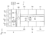
- 1 is a plan view schematically showing the outline of the configuration of a wafer processing system according to this embodiment
- FIG. FIG. 4 is an explanatory diagram showing how the first wafer is peeled off from the laser absorption layer
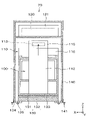
- 1 is a side view schematically showing the outline of the configuration of a wafer processing apparatus according to this embodiment
- FIG. 1 is a side view showing the schematic configuration of a wafer processing apparatus according to an embodiment
- FIG. 1 is a side view showing the schematic configuration of a wafer processing apparatus according to an embodiment
- FIG. 1 is a side view showing the schematic configuration of a wafer processing apparatus according to an embodiment
- FIG. 1 is a side view showing the arrangement of a wafer processing apparatus and a wafer transfer apparatus according to the embodiment
- wafers In the manufacturing process of semiconductor devices, semiconductor wafers (hereinafter referred to as "wafers") are processed by irradiating them with laser light. For example, laser processing is performed for various purposes such as transferring a device layer formed on the surface of one wafer to another wafer, so-called laser lift-off, and separating wafers.
- the laser oscillator is installed so as to extend in the horizontal direction. For this reason, when the size of the laser oscillator increases, the size of the laser processing apparatus increases in the horizontal direction, and the area occupied by the laser processing apparatus (footprint) increases. In such a case, the number of laser processing apparatuses that can be installed in the wafer processing space is reduced, resulting in a decrease in the number of wafers processed (the number of wafers produced).
- a holding table that holds a wafer, a processing head that irradiates a laser beam onto the wafer, and a laser oscillator that oscillates the laser beam are arranged in this order from below.
- the laser processing apparatus becomes large in the height direction, and the height position of the upper laser oscillator becomes high.
- the technology according to the present disclosure reduces the size of a substrate processing apparatus that processes a substrate by irradiating it with a laser beam.
- a wafer processing apparatus as a substrate processing apparatus, a wafer processing system as a substrate processing system, and a wafer processing method as a substrate processing method according to the present embodiment will be described below with reference to the drawings.
- elements having substantially the same functional configuration are denoted by the same reference numerals, thereby omitting redundant description.
- processing is performed on a superposed wafer T as a substrate in which a first wafer W and a second wafer S are bonded as shown in FIG.
- the surface of the first wafer W to be bonded to the second wafer S will be referred to as a front surface Wa
- the surface opposite to the front surface Wa will be referred to as a rear surface Wb.
- the surface on the side bonded to the first wafer W is referred to as a front surface Sa
- the surface opposite to the front surface Sa is referred to as a rear surface Sb.
- the first wafer W is, for example, a semiconductor wafer such as a silicon substrate.
- a laser absorption layer P On the surface Wa of the first wafer W, a laser absorption layer P, a device layer Dw, and a surface film Fw are laminated in this order from the surface Wa side.
- the laser absorption layer P absorbs laser light emitted from the laser irradiation mechanism 110 as described later.
- An oxide film (SiO 2 film) for example, is used for the laser absorption layer P, but there is no particular limitation as long as it absorbs laser light.
- the device layer Dw includes multiple devices. Examples of the surface film Fw include oxide films (SiO 2 film, TEOS film), SiC films, SiCN films, adhesives, and the like.
- the position of the laser absorption layer P is not limited to the above embodiment, and may be formed between the device layer Dw and the surface film Fw, for example. Moreover, the device layer Dw and the surface film Fw may not be formed on the surface Wa. In this case, the laser absorption layer P is formed on the second wafer S side, and the device layer Ds on the second wafer S side is transferred to the first wafer W side.
- the second wafer S is also a semiconductor wafer such as a silicon substrate.
- the device layer Ds and the surface film Fs are laminated in this order from the surface Sa side.
- the device layer Ds and the surface film Fs are the same as the device layer Dw and the surface film Fw of the first wafer W, respectively. Note that the device layer Ds and the surface film Fs may not be formed on the surface Sa. Then, the surface film Fw of the first wafer W and the surface film Fs of the second wafer S are bonded.
- the wafer processing system 1 has a configuration in which a loading/unloading station 2 and a processing station 3 are integrally connected.
- a loading/unloading station 2 for example, cassettes Ct, Cw, and Cs capable of accommodating a plurality of superposed wafers T, a plurality of first wafers W, and a plurality of second wafers S are loaded/unloaded from/to the outside.
- the processing station 3 includes various processing devices for performing desired processing on the superposed wafer T. FIG.
- a cassette mounting table 10 is provided in the loading/unloading station 2 .
- a plurality of cassettes Ct, Cw, and Cs can be freely placed in a row on the cassette placing table 10 in the Y-axis direction.
- the number of cassettes Ct, Cw, and Cs to be placed on the cassette placing table 10 can be determined arbitrarily.
- the loading/unloading station 2 is provided with a wafer transfer device 20 adjacent to the cassette mounting table 10 on the X-axis positive direction side of the cassette mounting table 10 .
- the wafer transfer device 20 has a transfer arm 21 that holds and transfers the superposed wafer T, the first wafer W, and the second wafer S. As shown in FIG. Then, the wafer transfer device 20 moves on a transfer path 22 extending in the Y-axis direction, and between the cassettes Ct, Cw, and Cs on the cassette mounting table 10 and the transition device 30, which will be described later, the superimposed wafers T and the first wafers.
- a wafer W and a second wafer S are configured to be transportable.
- Loading/unloading station 2 is adjacent to wafer transport device 20 on the X-axis positive direction side of wafer transport device 20 , and stacks superimposed wafer T, first wafer W, and second wafer S with processing station 3 .
- a transition device 30 is provided for passing between.
- the processing station 3 is provided with a wafer transfer device 40 as a substrate transfer device, a cleaning device 50, a peeling device 60, and wafer processing devices 70-73.
- the wafer transfer device 40 is arranged on the positive side of the transition device 30 in the X-axis direction.
- a cleaning device 50 and two wafer processing devices 70 and 71 are arranged side by side from the X-axis negative direction side to the positive direction side.
- a peeling device 60 and two wafer processing devices 72 and 73 are arranged side by side from the X-axis negative direction side toward the positive direction side.
- the wafer transfer device 40 has a transfer arm 41 that holds and transfers the overlapped wafer T, the first wafer W, and the second wafer S.
- the wafer transfer device 40 moves on a transfer path 42 extending in the X-axis direction, and transfers the overlapped wafer T to the transition device 30, the cleaning device 50, the peeling device 60, and the wafer processing devices 70 to 73 of the loading/unloading station 2. can be transported.
- the cleaning device 50 cleans the surface of the laser absorption layer P formed on the surface Sa of the second wafer S separated by the separation device 60 . Further, the cleaning device 50 may have a configuration for cleaning the back surface Sb of the second wafer S as well as the front surface Sa.
- the peeling device 60 peels the first wafer W from the second wafer S with respect to the superimposed wafer T laser-processed by the wafer processing devices 70-73.
- the wafer processing apparatuses 70 to 73 irradiate the laser absorption layer P of the first wafer W with laser light to cause delamination at the interface between the laser absorption layer P and the first wafer W.
- the configuration of the wafer processing apparatuses 70 to 73 will be described later.
- a controller 80 is provided in the wafer processing system 1 described above.
- the control unit 80 is, for example, a computer equipped with a CPU, memory, etc., and has a program storage unit (not shown).
- the program storage unit stores programs for controlling the processing of the superposed wafers T in the wafer processing system 1 .
- the program may be recorded in a computer-readable storage medium H and installed in the control unit 80 from the storage medium H. Further, the storage medium H may be temporary or non-temporary.
- the first wafer W and the second wafer S are bonded together in a bonding apparatus (not shown) outside the wafer processing system 1 to form a superimposed wafer T in advance.
- a cassette Ct containing a plurality of superposed wafers T is mounted on the cassette mounting table 11 of the loading/unloading station 2 .
- the superposed wafer T in the cassette Ct is taken out by the wafer transfer device 20, transferred to the transition device 30, and further transferred to the wafer processing device 70 by the wafer transfer device 40.
- a laser beam L CO 2 laser light
- the entire surface of the laser absorption layer P is irradiated with the laser light L.
- the laser light L is transmitted through the first wafer W from the rear surface Wb side of the first wafer W and is absorbed in the laser absorption layer P.
- This laser light L causes peeling at the interface between the laser absorption layer P and the first wafer W.
- the superposed wafer T is transferred to the peeling device 60 by the wafer transfer device 40 .
- a suction pad (not shown) sucks and holds the rear surface Wb of the first wafer W as shown in FIG.
- the first wafer W is separated.
- the separated first wafer W is transferred to the transition device 30 by the wafer transfer device 40 and further transferred to the cassette Cw on the cassette mounting table 11 by the wafer transfer device 20 .
- the first wafer W unloaded from the peeling device 60 may be transferred to the cleaning device 50 before being transferred to the cassette Cw, and the front surface Wa, which is the peeling surface, may be cleaned.
- the separated second wafer S is transferred to the cleaning device 50 by the wafer transfer device 40 .
- the surface of the laser absorption layer P which is the peeling surface, is cleaned.
- the back surface Sb of the second wafer S may be cleaned together with the front surface of the laser absorption layer P.
- separate cleaning units may be provided for cleaning the front surface of the laser absorption layer P and the back surface Sb of the second wafer S, respectively.
- the second wafer S that has undergone all the processes is transferred by the wafer transfer device 40 to the transition device 30 and further transferred by the wafer transfer device 20 to the cassette Cs of the cassette mounting table 11 .
- a series of wafer processing in the wafer processing system 1 is completed.
- the wafer processing apparatus 70 has a stage 100, a laser irradiation mechanism 110, and electrical equipment 120.
- the stage 100 is a stage for holding and processing the superposed wafer T.
- FIG. The laser irradiation mechanism 110 irradiates the superposed wafer T held on the stage 100 with laser light.
- the stage 100 has a chuck 101 as a substrate holder, an air bearing 102, a slider table 103, a rotating mechanism 104, a moving mechanism 105, rails 106, and a base 107.
- the chuck 101 holds the superposed wafer T on its upper surface and holds the rear surface Sb of the second wafer S by suction.
- a chuck 101 is supported by a slider table 103 via an air bearing 102 .
- a rotating mechanism 104 is provided on the lower surface side of the slider table 103 .
- the rotation mechanism 104 incorporates, for example, a motor as a drive source.
- the chuck 101 is configured to be rotatable around the ⁇ axis (vertical axis) via an air bearing 102 by a rotating mechanism 104 .
- the slider table 103 is configured to be movable along a rail 106 extending in the X-axis direction by a moving mechanism 105 provided on the underside thereof. Rail 106 is provided on base 107 .
- the driving source of the moving mechanism 105 is not particularly limited, for example, a linear motor is used.
- the laser irradiation mechanism 110 has a laser irradiation lens 111 , a laser oscillator 112 , a mirror 113 and an optical system 114 .
- the laser irradiation lens 111 is arranged above the chuck 101 .
- the laser irradiation lens 111 is, for example, a cylindrical member, and irradiates the superposed wafer T held by the chuck 101 with laser light.
- the laser light emitted from the laser irradiation lens 111 passes through the first wafer W, and the laser absorption layer P is irradiated with the laser light.
- the laser irradiation lens 111 may be configured to be vertically movable by a lifting mechanism (not shown).
- the laser oscillator 112 oscillates and emits pulsed laser light. That is, this laser light is a so-called pulse laser. Also, in this embodiment, the laser light is CO 2 laser light, and the wavelength of the CO 2 laser light is, for example, 8.9 ⁇ m to 11 ⁇ m.
- the mirror 113 redirects the laser light emitted from the laser oscillator 112 in the direction of the optical system 114, that is, in the horizontal direction as described later.
- the emission position and emission direction of the laser light from the laser oscillator 112 may change. Even in such a case, the direction of the laser beam can be corrected by the mirror 113 without changing the optical system 114 .
- the mirror 113 is housed in a mirror box 115 .
- the optical system 114 adjusts the output of the laser light incident from the mirror 113 and guides the laser light to the laser irradiation lens 111 .
- the optical system 114 is housed in an optical system box 116 .
- the optical system 114 includes, for example, a plurality of mirrors, a beam expander, DOEs (Diffractive Optical Elements), and the like. These components of the optical system 114 are arranged horizontally on the bottom surface inside the optical system box 116 as shown in FIG.
- the laser light incident from the mirror 113 is emitted downward through the optical system 114 and guided to the laser irradiation lens 111 .
- the top plate 116a of the optical system box 116 is detachable. The inside of the optical system box 116 can be accessed horizontally and from above with the top plate 116a removed (block arrow in FIG. 6), and maintenance of the optical system 114, for example, is performed.
- the electrical components 120 are electrical components used in each part of the wafer processing apparatus 70, and include electrical components used in the stage 100 or the laser irradiation mechanism 110.
- the electrical component 120 is housed in an electrical component box 121 .
- the wafer processing apparatus 70 further includes a support frame 130 and a connecting frame 140, as shown in FIGS.
- Support frame 130 supports at least stage 100 and laser oscillator 112 .
- the connection frame 140 is provided outside the support frame 130 so as to surround the support frame 130 .
- the support frame 130 includes an upper support frame 131 and a lower support frame 132.
- An insulator 133 is provided between the upper support frame 131 and the lower support frame 132 .
- Anti-vibration rubber for example, is used for the insulator 133 .
- This insulator 133 suppresses transmission of vibration of the lower support frame 132 to the upper support frame 131 .
- the upper support frame 131 is divided into a first support area 131S where the stage 100 is arranged on the Y-axis negative direction side and a second support area 131T where the laser oscillator 112 is arranged on the Y-axis positive direction side.
- the first support area 131S is an area composed of beams 131a, 131b, 131c and columns 131d, 131e.
- the beams 131a, 131b, and 131c are arranged in three stages in this order from below.
- the columns 131d and 131e are arranged in this order from the Y-axis negative direction to the positive direction.
- the second support region 131T is a region composed of beams 131f and columns 131e. Beam 131f may be the same as beam 131a, or may be connected to beam 131a.
- the stage 100 is supported by the middle beam 131b, and the optical system box 116 is supported by the upper beam 131c. That is, the optical system box 116 is arranged above the stage 100 .
- a laser oscillator 112 is supported by the beam 131f in the second support region 131T.
- Laser oscillator 112 may be supported by column 131e.
- the laser oscillator 112 is provided so as to extend in the height direction.
- An electrical cable, a cooling water supply pipe, and the like are connected to the lower portion of the laser oscillator 112, and a space for installing these is secured.
- the mirror box 115 is laminated on the laser oscillator 112 .
- the stage 100 and the laser oscillator 112 are arranged side by side in the horizontal direction. At least part of the stage 100 and part of the laser oscillator 112 are at the same height, that is, the stage 100 and the laser oscillator 112 overlap in the height direction when viewed from the side. Also, the optical system box 116 and the mirror box 115 are arranged side by side in the horizontal direction, and in this embodiment, the upper surface of the optical system box 116 and the upper surface of the mirror box 115 are at the same height.
- the components of the laser irradiation mechanism 110 are arranged as described above.
- the laser beam L is emitted from the laser oscillator 112 upward from the wafer holding surface of the chuck 101 on the stage 100 .
- a laser beam L from a laser oscillator 112 enters a mirror box 115 above the stage 100 and is redirected horizontally (negative Y-axis direction) by a mirror 113 .
- the laser light L from the mirror box 115 enters the optical system box 116, and after the output of the laser light L is adjusted by the optical system 114, it is guided to the laser irradiation lens 111 provided below. Then, the superposed wafer T held by the chuck 101 is irradiated with the laser light L from the laser irradiation lens 111 .
- Connecting members 134 connected to the lower end of the connecting frame 140 are provided at the four corners of the lower end of the lower support frame 132 .
- Casters 135 are provided on the lower surface of the connecting member 134, and the support frame 130 and the components supported by the support frame 130 are configured to be independently movable.
- the electrical component box 121 is supported by the connecting frame 140 .
- the electrical equipment box 121 is supported on the uppermost stage of the connecting frame 140 , that is, arranged above the stage 100 and the laser irradiation mechanism 110 supported by the upper support frame 131 .
- the connecting members 134 are connected to the four corners of the lower end of the connecting frame 140 as described above.
- Casters 141 are provided at the lower end of the connecting frame 140, and the connecting frame 140 and components supported by the connecting frame 140 are configured to be independently movable.
- connection frame 140 of the wafer processing equipment 70 is connected to the frames of adjacent equipment. That is, the connection frame 140 is connected to the connection frame 140 of the wafer processing device 71 , the frame (not shown) of the cleaning device 50 , and the frame 150 of the wafer transfer area that accommodates the wafer transfer device 40 .
- the other wafer processing apparatuses 71 to 73 also have the same configuration as the wafer processing apparatus 70 described above. However, the wafer processing apparatuses 70 and 71 and the wafer processing apparatuses 72 and 73 have different orientations in the Y-axis direction. As shown in FIG. 7, the wafer processing device 70 and the wafer processing device 72 are provided facing each other with the wafer transfer device 40 interposed therebetween. In this case, the laser oscillator 112 of the wafer processing device 72, the stage 100, the wafer transfer device 40, the stage 100 of the wafer processing device 70, and the laser oscillator 112 are arranged in this order from the positive direction side to the negative direction side in the Y-axis direction. is placed in Also, the arrangement of the wafer processing equipment 71 and the wafer processing equipment 73 is the same.
- the laser oscillator 112 extends in the height direction and is provided so that the emission direction of the laser light is directed upward. Even if it does, the wafer processing apparatus 70 can be miniaturized. The effect of this embodiment will be described below in comparison with a conventional wafer processing apparatus.
- a laser oscillator extends horizontally.
- a laser oscillator is provided above the stage.
- the laser oscillator is arranged to extend in the horizontal direction (the X-axis direction in this embodiment).
- the laser oscillator, the laser optical system, and the controller of the driving unit are arranged side by side in the X-axis direction.
- the width of the laser oscillator in the X-axis direction becomes large, and the width of the wafer processing apparatus in the X-axis direction becomes large.
- stacking a laser oscillator, a laser optical system box, and a control unit including electrical components in order to reduce the width of the wafer processing apparatus in the X-axis direction increases the height of the wafer processing apparatus.
- the width in the X-axis direction in this embodiment is large, so the area occupied by the wafer processing apparatus is large.
- the number of wafer processing apparatuses will be reduced due to restrictions on the width in the X-axis direction at the installation site. As a result, the number of processed wafers is reduced.
- the height of the conventional wafer processing equipment increases, and the installation height position of the laser oscillator increases.
- the laser oscillator which is a heavy object, must be removed at a high place and further installed. As a result, maintenance of the laser oscillator takes time and effort.
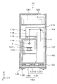
- the laser oscillator 112 is provided so as to extend in the height direction, as shown in FIGS. Therefore, even if the laser oscillator 112 is enlarged, the width A of the wafer processing apparatus 70 in the X-axis direction can be made smaller than the width of the conventional wafer processing apparatus, and the area occupied by the wafer processing apparatus 70 can be reduced. can do.
- the length B of the wafer processing apparatus 70 in the Y-axis direction is also less than the length of the conventional wafer processing apparatus. In such a case, for example, the number of wafer processing apparatuses 70 that can be installed in the wafer processing system 1 of the present embodiment increases, for example, four. As a result, the number of overlapping wafers T to be processed can be increased.
- the height H of the wafer processing apparatus 70 is also smaller than that of the conventional wafer processing apparatus, and the height position of the laser oscillator 112 can be lowered. Specifically, for example, a worker can directly access the laser oscillator 112 . In particular, since the laser oscillator 112 is provided on the side opposite to the wafer transfer device 40, the operator can easily access the laser oscillator 112. FIG. As a result, the maintenance of the laser oscillator 112 can be carried out in a short period of time without taking much time and effort, and the efficiency of maintenance can be improved.
- the optical system box 116 can be accessed from both the horizontal direction and the top with the top plate 116a removed (see the block in FIG. 6). arrow), which can also improve accessibility. As a result, the efficiency of maintenance of the optical system 114 of the optical system box 116 can be improved.
- connection frame 140 of the wafer processing apparatus 70 is connected to the frame 150 of the wafer transfer area.
- the vibration is transmitted to the connecting frame 140 of the wafer processing device 70 via the frame 150 of the wafer transfer area.
- the connection frame 140 since the connection frame 140 is connected to the support frame 130 only by the connection member 134, transmission of the vibration of the connection frame 140 to the support frame 130 can be suppressed.
- the upper support frame 131 supports the stage 100 and the laser irradiation mechanism 110 .
- the upper support frame 131 vibrates, it is possible to suppress the amplitude deviation and phase deviation between the superposed wafer T held by the chuck 101 of the stage 100 and the laser irradiation lens 111 (processing point). . Therefore, when laser light is irradiated from the laser irradiation lens 111 to the laser absorption layer P of the superposed wafer T, meandering of the laser light can be suppressed, and displacement of the laser light can be suppressed. As a result, laser processing on the superposed wafer T can be performed accurately and appropriately.
- the mirror box 115 is arranged side by side with the optical system box 116.
- the mirror box 115 is arranged as in this embodiment.
- the width A of the wafer processing apparatus 70 in the X-axis direction can be made smaller than the width of the conventional wafer processing apparatus, and the area occupied by the wafer processing apparatus 70 can be reduced.
- the height position of the laser oscillator 112 is slightly higher than the height position of the laser oscillator 112 in the above-described embodiment, the height position of the laser oscillator 112 can still be lower than in the conventional wafer processing apparatus. .
- the configuration of the optical system 114 and the optical system box 116 may be as shown in FIG.
- the optical system 114 is composed of, for example, a plurality of mirrors, a beam expander, a DOE, etc., as described above. These components of the optical system 114 are arranged vertically on the side surface of the optical system box 116 on the side of the laser oscillator 112 and the mirror box 115, and a mirror is arranged horizontally on the bottom surface.
- the laser light incident from the mirror 113 is emitted downward through the optical system 114 and guided to the laser irradiation lens 111 .
- a side wall 116b of the optical system box 116 opposite to the laser oscillator 112 is detachable. With the side wall 116b removed, the interior of the optical system box 116 can be accessed from the horizontal direction (block arrow in FIG. 10).
- access to the inside of the optical system box 116 can be made from the horizontal direction, and the components of the optical system 114 are arranged in the vertical direction, so that accessibility can be improved. As a result, the efficiency of maintenance of the optical system 114 of the optical system box 116 can be improved.
- the optical system box 116 having the detachable side wall 116b as in the present embodiment can also be applied when the mirror box 115 is provided above the optical system box 116 as shown in FIGS. .
Abstract
Description
70~73 ウェハ処理装置
100 ステージ
101 チャック
111 レーザ照射レンズ
112 レーザ発振器
113 ミラー
114 光学系
T 重合ウェハ
W 第1のウェハ
S 第2のウェハ
Claims (16)
- 基板にレーザ光を照射して当該基板を処理する基板処理装置であって、
前記基板を保持する基板保持部と、
前記基板保持部に保持された前記基板にレーザ光を照射するレーザ照射レンズと、
前記基板保持部の基板保持面よりも上方向に向けてレーザ光を出射するレーザ発振器と、
前記基板保持部の上方において、前記レーザ発振器から出射されたレーザ光を水平方向に方向変更するミラーと、
前記ミラーから入射するレーザ光の出力を調整し、かつ当該レーザ光を前記レーザ照射レンズへ導く光学系と、を有する、基板処理装置。 - 前記基板保持部と前記レーザ発振器を支持する支持フレームを有する、請求項1に記載の基板処理装置。
- 前記基板保持部と前記レーザ発振器は水平方向に並べて配置され、
少なくとも前記基板保持部の一部と前記レーザ発振器の一部は同一高さにある、請求項2に記載の基板処理装置。 - 前記ミラーを収容するミラーボックスと、
前記光学系を収容する光学系ボックスと、を有する、請求項2又は3に記載の基板処理装置。 - 前記光学系は、前記光学系ボックスの内部において前記レーザ発振器側の側面に配置され、
前記光学系ボックスは、当該光学系ボックスの内部に前記レーザ発振器と反対側の側面からアクセス可能に構成されている、請求項4に記載の基板処理装置。 - 前記支持フレームは、前記ミラーボックスと前記光学系ボックスを支持する、請求項4又は5に記載の基板処理装置。
- 前記支持フレームは上部支持フレームと下部支持フレームを含み、
前記上部支持フレームと前記下部支持フレームの間にはインシュレータが設けられている、請求項2~6のいずれか一項に記載の基板処理装置。 - 前記支持フレームの外側に設けられた連結フレームを有し、
前記下部支持フレームと前記連結フレームが接続されている、請求項7に記載の基板処理装置。 - 電装品を収容する電装品ボックスを有し、
前記電装品ボックスは、前記基板保持部と前記レーザ発振器の上方において前記連結フレームに支持されている、請求項8に記載の基板処理装置。 - 基板処理システムであって、
基板にレーザ光を照射して当該基板を処理する基板処理装置と、
前記基板処理装置に前記基板を搬送する基板搬送装置と、を有し、
前記基板処理装置は、
前記基板を保持する基板保持部と、
前記基板保持部に保持された前記基板にレーザ光を照射するレーザ照射レンズと、
前記基板保持部の基板保持面よりも上方向に向けてレーザ光を出射するレーザ発振器と、
前記基板保持部の上方において、前記レーザ発振器から出射されたレーザ光を水平方向に方向変更するミラーと、
前記ミラーから入射するレーザ光の出力を調整し、かつ当該レーザ光を前記レーザ照射レンズへ導く光学系と、を有する、基板処理システム。 - 前記基板処理装置を複数有し、
前記基板保持部と前記レーザ発振器を支持する支持フレームと、
前記支持フレームの外側に設けられた連結フレームと、を有し、
前記連結フレームは水平方向に並べて複数配置される、請求項10に記載の基板処理システム。 - 前記基板保持部と前記レーザ発振器を支持する支持フレームと、
前記支持フレームの外側に設けられた連結フレームと、
前記基板搬送装置を収容する基板搬送領域のフレームと、を有し、
前記連結フレームと、前記基板搬送領域のフレームは水平方向に並べて配置される、請求項10に記載の基板処理システム。 - 前記基板搬送装置、前記基板保持部及び前記レーザ発振器は、水平方向にこの順で並べて配置されている、請求項10~12のいずれか一項に記載の基板処理システム。
- 前記レーザ発振器、前記基板保持部、前記基板搬送装置、前記基板保持部及び前記レーザ発振器は、水平方向にこの順で並べて配置されている、請求項10~12のいずれか一項に記載の基板処理システム。
- 少なくとも前記基板保持部の一部と前記レーザ発振器の一部は同一高さにある、請求項13又は14に記載の基板処理システム。
- 基板にレーザ光を照射して当該基板を処理する基板処理方法であって、
基板保持部で基板を保持することと、
レーザ発振器から前記基板保持部の基板保持面よりも上方向に向けてレーザ光を出射することと、
前記基板保持部の上方において、ミラーを用いて前記レーザ発振器から出射されたレーザ光を水平方向に方向変更することと、
光学系を用いて、前記ミラーから入射するレーザ光の出力を調整し、かつ当該レーザ光をレーザ照射レンズへ導くことと、
前記レーザ照射レンズから前記基板保持部に保持された前記基板にレーザ光を照射することと、を有する、基板処理方法。
Priority Applications (3)
| Application Number | Priority Date | Filing Date | Title |
|---|---|---|---|
| CN202280017660.3A CN116887943A (zh) | 2021-03-12 | 2022-02-28 | 基板处理装置、基板处理系统以及基板处理方法 |
| JP2023505301A JPWO2022190924A1 (ja) | 2021-03-12 | 2022-02-28 | |
| KR1020237034609A KR20230157399A (ko) | 2021-03-12 | 2022-02-28 | 기판 처리 장치, 기판 처리 시스템 및 기판 처리 방법 |
Applications Claiming Priority (2)
| Application Number | Priority Date | Filing Date | Title |
|---|---|---|---|
| JP2021040497 | 2021-03-12 | ||
| JP2021-040497 | 2021-03-12 |
Publications (1)
| Publication Number | Publication Date |
|---|---|
| WO2022190924A1 true WO2022190924A1 (ja) | 2022-09-15 |
Family
ID=83226622
Family Applications (1)
| Application Number | Title | Priority Date | Filing Date |
|---|---|---|---|
| PCT/JP2022/008206 WO2022190924A1 (ja) | 2021-03-12 | 2022-02-28 | 基板処理装置、基板処理システム及び基板処理方法 |
Country Status (4)
| Country | Link |
|---|---|
| JP (1) | JPWO2022190924A1 (ja) |
| KR (1) | KR20230157399A (ja) |
| CN (1) | CN116887943A (ja) |
| WO (1) | WO2022190924A1 (ja) |
Citations (7)
| Publication number | Priority date | Publication date | Assignee | Title |
|---|---|---|---|---|
| JPH0335511Y2 (ja) * | 1987-11-06 | 1991-07-26 | ||
| JP2010501354A (ja) * | 2006-08-22 | 2010-01-21 | ジーエスアイ・グループ・コーポレーション | X−y高速穴あけシステム |
| JP2011187481A (ja) * | 2010-03-04 | 2011-09-22 | Disco Corp | 加工装置 |
| JP2011230179A (ja) * | 2010-04-30 | 2011-11-17 | Mitsuboshi Diamond Industrial Co Ltd | レーザ加工装置の光軸調整方法 |
| JP2017042805A (ja) * | 2015-08-28 | 2017-03-02 | 株式会社ディスコ | レーザー加工装置 |
| JP2019188455A (ja) * | 2018-04-27 | 2019-10-31 | 三星ダイヤモンド工業株式会社 | レーザ光軸確認用治具ユニット並びに治具 |
| WO2020213479A1 (ja) * | 2019-04-19 | 2020-10-22 | 東京エレクトロン株式会社 | 処理装置及び処理方法 |
-
2022
- 2022-02-28 CN CN202280017660.3A patent/CN116887943A/zh active Pending
- 2022-02-28 KR KR1020237034609A patent/KR20230157399A/ko unknown
- 2022-02-28 JP JP2023505301A patent/JPWO2022190924A1/ja active Pending
- 2022-02-28 WO PCT/JP2022/008206 patent/WO2022190924A1/ja active Application Filing
Patent Citations (7)
| Publication number | Priority date | Publication date | Assignee | Title |
|---|---|---|---|---|
| JPH0335511Y2 (ja) * | 1987-11-06 | 1991-07-26 | ||
| JP2010501354A (ja) * | 2006-08-22 | 2010-01-21 | ジーエスアイ・グループ・コーポレーション | X−y高速穴あけシステム |
| JP2011187481A (ja) * | 2010-03-04 | 2011-09-22 | Disco Corp | 加工装置 |
| JP2011230179A (ja) * | 2010-04-30 | 2011-11-17 | Mitsuboshi Diamond Industrial Co Ltd | レーザ加工装置の光軸調整方法 |
| JP2017042805A (ja) * | 2015-08-28 | 2017-03-02 | 株式会社ディスコ | レーザー加工装置 |
| JP2019188455A (ja) * | 2018-04-27 | 2019-10-31 | 三星ダイヤモンド工業株式会社 | レーザ光軸確認用治具ユニット並びに治具 |
| WO2020213479A1 (ja) * | 2019-04-19 | 2020-10-22 | 東京エレクトロン株式会社 | 処理装置及び処理方法 |
Also Published As
| Publication number | Publication date |
|---|---|
| JPWO2022190924A1 (ja) | 2022-09-15 |
| KR20230157399A (ko) | 2023-11-16 |
| CN116887943A (zh) | 2023-10-13 |
Similar Documents
| Publication | Publication Date | Title |
|---|---|---|
| JP6679157B2 (ja) | 加工装置の搬送機構 | |
| TWI793322B (zh) | 工件分離裝置及工件分離方法 | |
| JP2021106197A (ja) | 基板処理装置及び基板処理方法 | |
| JP7218055B2 (ja) | チャックテーブル | |
| WO2022190924A1 (ja) | 基板処理装置、基板処理システム及び基板処理方法 | |
| JP2018181951A (ja) | 加工装置 | |
| KR20220048018A (ko) | 접합 장치, 접합 시스템 및 접합 방법 | |
| JP2004281430A (ja) | 紫外線照射方法およびそれを用いた装置 | |
| JP2022090272A (ja) | ウエーハ生成装置 | |
| JP7140576B2 (ja) | ウェーハの分割方法 | |
| JP4345476B2 (ja) | 露光装置 | |
| JP2018067668A (ja) | シート拡張装置 | |
| US20240162061A1 (en) | Substrate processing apparatus, substrate processing system, and substrate processing method | |
| JP5872799B2 (ja) | レーザー加工装置 | |
| KR101146642B1 (ko) | 곡면 밀착을 이용한 대상물 브레이킹장치 | |
| TWI747296B (zh) | 法蘭盤端面修正裝置、切斷裝置、法蘭盤端面修正方法以及切斷品的製造方法 | |
| JP2022091504A (ja) | レーザ照射システム、基板処理装置及び基板処理方法 | |
| JP7449097B2 (ja) | レーザー加工装置 | |
| JP4871336B2 (ja) | 露光装置 | |
| JP2008053531A (ja) | 半導体チップの実装装置 | |
| KR20230120097A (ko) | 웨이퍼의 가공 방법 | |
| JP7285151B2 (ja) | 支持体剥離方法及び支持体剥離システム | |
| JP2012199442A (ja) | ダイボンダ及び半導体製造方法 | |
| JP5386276B2 (ja) | 切削装置 | |
| JP6804146B2 (ja) | 搬送装置、加工装置及び搬送方法 |
Legal Events
| Date | Code | Title | Description |
|---|---|---|---|
| 121 | Ep: the epo has been informed by wipo that ep was designated in this application |
Ref document number: 22766883 Country of ref document: EP Kind code of ref document: A1 |
|
| WWE | Wipo information: entry into national phase |
Ref document number: 202280017660.3 Country of ref document: CN |
|
| WWE | Wipo information: entry into national phase |
Ref document number: 2023505301 Country of ref document: JP |
|
| WWE | Wipo information: entry into national phase |
Ref document number: 18549934 Country of ref document: US |
|
| ENP | Entry into the national phase |
Ref document number: 20237034609 Country of ref document: KR Kind code of ref document: A |
|
| WWE | Wipo information: entry into national phase |
Ref document number: 1020237034609 Country of ref document: KR |
|
| NENP | Non-entry into the national phase |
Ref country code: DE |
|
| 122 | Ep: pct application non-entry in european phase |
Ref document number: 22766883 Country of ref document: EP Kind code of ref document: A1 |