WO2023238542A1 - 基板処理システム及び基板処理方法 - Google Patents
基板処理システム及び基板処理方法 Download PDFInfo
- Publication number
- WO2023238542A1 WO2023238542A1 PCT/JP2023/016360 JP2023016360W WO2023238542A1 WO 2023238542 A1 WO2023238542 A1 WO 2023238542A1 JP 2023016360 W JP2023016360 W JP 2023016360W WO 2023238542 A1 WO2023238542 A1 WO 2023238542A1
- Authority
- WO
- WIPO (PCT)
- Prior art keywords
- substrate
- wafer
- separation
- irradiation
- laser beam
- Prior art date
Links
- 239000000758 substrate Substances 0.000 title claims abstract description 210
- 238000012545 processing Methods 0.000 title claims abstract description 78
- 238000003672 processing method Methods 0.000 title claims description 16
- 238000000926 separation method Methods 0.000 claims abstract description 133
- 230000007246 mechanism Effects 0.000 claims abstract description 86
- 238000001514 detection method Methods 0.000 claims abstract description 28
- 238000000034 method Methods 0.000 claims abstract description 25
- 238000012546 transfer Methods 0.000 claims description 65
- 230000032258 transport Effects 0.000 claims description 45
- 230000001678 irradiating effect Effects 0.000 claims description 31
- 238000005259 measurement Methods 0.000 claims description 20
- 230000002265 prevention Effects 0.000 claims description 12
- 230000001133 acceleration Effects 0.000 claims description 11
- 238000006073 displacement reaction Methods 0.000 claims description 10
- 230000007723 transport mechanism Effects 0.000 claims description 10
- 230000003595 spectral effect Effects 0.000 claims description 7
- 238000004458 analytical method Methods 0.000 claims description 5
- 230000015572 biosynthetic process Effects 0.000 claims description 5
- 235000012431 wafers Nutrition 0.000 description 641
- 238000010521 absorption reaction Methods 0.000 description 93
- 238000003384 imaging method Methods 0.000 description 43
- 238000004140 cleaning Methods 0.000 description 33
- 230000002093 peripheral effect Effects 0.000 description 31
- 238000005516 engineering process Methods 0.000 description 17
- 238000010586 diagram Methods 0.000 description 13
- 238000004364 calculation method Methods 0.000 description 12
- 239000004065 semiconductor Substances 0.000 description 11
- 230000003287 optical effect Effects 0.000 description 8
- XUIMIQQOPSSXEZ-UHFFFAOYSA-N Silicon Chemical compound [Si] XUIMIQQOPSSXEZ-UHFFFAOYSA-N 0.000 description 6
- 229910052710 silicon Inorganic materials 0.000 description 6
- 239000010703 silicon Substances 0.000 description 6
- 230000003247 decreasing effect Effects 0.000 description 5
- 238000004611 spectroscopical analysis Methods 0.000 description 3
- 238000001228 spectrum Methods 0.000 description 3
- 238000003860 storage Methods 0.000 description 3
- 229910004298 SiO 2 Inorganic materials 0.000 description 2
- 230000007423 decrease Effects 0.000 description 2
- 238000010438 heat treatment Methods 0.000 description 2
- 238000007689 inspection Methods 0.000 description 2
- 238000013532 laser treatment Methods 0.000 description 2
- 239000007788 liquid Substances 0.000 description 2
- 238000004519 manufacturing process Methods 0.000 description 2
- 230000001737 promoting effect Effects 0.000 description 2
- BOTDANWDWHJENH-UHFFFAOYSA-N Tetraethyl orthosilicate Chemical compound CCO[Si](OCC)(OCC)OCC BOTDANWDWHJENH-UHFFFAOYSA-N 0.000 description 1
- 239000000853 adhesive Substances 0.000 description 1
- 230000001070 adhesive effect Effects 0.000 description 1
- 238000013459 approach Methods 0.000 description 1
- 230000000052 comparative effect Effects 0.000 description 1
- 238000012937 correction Methods 0.000 description 1
- 230000003028 elevating effect Effects 0.000 description 1
- 238000002474 experimental method Methods 0.000 description 1
- 238000003780 insertion Methods 0.000 description 1
- 230000037431 insertion Effects 0.000 description 1
- 239000000463 material Substances 0.000 description 1
- 238000011946 reduction process Methods 0.000 description 1
- 230000000630 rising effect Effects 0.000 description 1
- 238000004904 shortening Methods 0.000 description 1
- 238000004088 simulation Methods 0.000 description 1
Images


Classifications
-
- B—PERFORMING OPERATIONS; TRANSPORTING
- B23—MACHINE TOOLS; METAL-WORKING NOT OTHERWISE PROVIDED FOR
- B23K—SOLDERING OR UNSOLDERING; WELDING; CLADDING OR PLATING BY SOLDERING OR WELDING; CUTTING BY APPLYING HEAT LOCALLY, e.g. FLAME CUTTING; WORKING BY LASER BEAM
- B23K26/00—Working by laser beam, e.g. welding, cutting or boring
- B23K26/50—Working by transmitting the laser beam through or within the workpiece
- B23K26/57—Working by transmitting the laser beam through or within the workpiece the laser beam entering a face of the workpiece from which it is transmitted through the workpiece material to work on a different workpiece face, e.g. for effecting removal, fusion splicing, modifying or reforming
-
- H—ELECTRICITY
- H01—ELECTRIC ELEMENTS
- H01L—SEMICONDUCTOR DEVICES NOT COVERED BY CLASS H10
- H01L21/00—Processes or apparatus adapted for the manufacture or treatment of semiconductor or solid state devices or of parts thereof
- H01L21/02—Manufacture or treatment of semiconductor devices or of parts thereof
- H01L21/04—Manufacture or treatment of semiconductor devices or of parts thereof the devices having at least one potential-jump barrier or surface barrier, e.g. PN junction, depletion layer or carrier concentration layer
- H01L21/18—Manufacture or treatment of semiconductor devices or of parts thereof the devices having at least one potential-jump barrier or surface barrier, e.g. PN junction, depletion layer or carrier concentration layer the devices having semiconductor bodies comprising elements of Group IV of the Periodic System or AIIIBV compounds with or without impurities, e.g. doping materials
- H01L21/30—Treatment of semiconductor bodies using processes or apparatus not provided for in groups H01L21/20 - H01L21/26
- H01L21/302—Treatment of semiconductor bodies using processes or apparatus not provided for in groups H01L21/20 - H01L21/26 to change their surface-physical characteristics or shape, e.g. etching, polishing, cutting
- H01L21/304—Mechanical treatment, e.g. grinding, polishing, cutting
-
- H—ELECTRICITY
- H01—ELECTRIC ELEMENTS
- H01L—SEMICONDUCTOR DEVICES NOT COVERED BY CLASS H10
- H01L21/00—Processes or apparatus adapted for the manufacture or treatment of semiconductor or solid state devices or of parts thereof
- H01L21/67—Apparatus specially adapted for handling semiconductor or electric solid state devices during manufacture or treatment thereof; Apparatus specially adapted for handling wafers during manufacture or treatment of semiconductor or electric solid state devices or components ; Apparatus not specifically provided for elsewhere
- H01L21/683—Apparatus specially adapted for handling semiconductor or electric solid state devices during manufacture or treatment thereof; Apparatus specially adapted for handling wafers during manufacture or treatment of semiconductor or electric solid state devices or components ; Apparatus not specifically provided for elsewhere for supporting or gripping
Definitions
- the present disclosure relates to a substrate processing system and a substrate processing method.
- Patent Document 1 discloses that in a semiconductor substrate on which a peeled oxide film and a semiconductor element are formed, the semiconductor element is transferred to a transfer destination substrate.
- the method described in Patent Document 1 includes a step of locally heating the peeled oxide film by irradiating light from the back surface of the semiconductor substrate, and a step of heating the peeled oxide film locally and/or at the interface between the peeled oxide film and the semiconductor substrate. and transferring the semiconductor element to the transfer destination substrate.
- the technology according to the present disclosure appropriately determines whether or not the substrates are separated after irradiation with laser light and before separation of the substrates, when separating substrates based on a separation plane formed by irradiation with laser light. Detect.
- One aspect of the present disclosure is a substrate processing system that processes a substrate, including a substrate holder having a holding surface that holds the substrate, a drive mechanism that moves the substrate holder in a horizontal direction, and a drive mechanism that moves the substrate holder in a horizontal direction. a rotation mechanism that rotates the substrate; a laser irradiation unit that irradiates the substrate held on the holding surface with a laser beam to form a separation surface that serves as a base point for separation of the substrate; The substrate includes a detection mechanism that detects separation based on the separation surface.
- the present disclosure when separating substrates based on a separation plane formed by irradiation with laser light, it is appropriately detected whether the substrates are separated after irradiation with laser light and before separation of the substrates. can.
- FIG. 2 is a side view schematically showing the configuration of a polymerized wafer to be processed.
- FIG. 1 is a plan view schematically showing the configuration of a wafer processing system.
- FIG. 1 is a perspective view schematically showing the configuration of a wafer transfer device.
- FIG. 2 is a side view schematically showing the configuration of a laser irradiation device.
- FIG. 2 is a plan view schematically showing the configuration of a laser irradiation device.
- FIG. 3 is an explanatory diagram showing eccentricity of a first wafer and a second wafer.
- FIG. 3 is a side view showing how the separation device operates.
- FIG. 2 is an explanatory diagram showing how a laser absorption layer is irradiated with laser light.
- FIG. 1 is a plan view schematically showing the configuration of a wafer processing system.
- FIG. 1 is a perspective view schematically showing the configuration of a wafer transfer device.
- FIG. 2 is a side view schematically
- FIG. 3 is a flow diagram showing the main steps of wafer processing. It is an explanatory view showing an example of irradiation of a laser beam to a laser absorption layer.
- FIG. 3 is an explanatory diagram of an unirradiated area generated in a laser absorption layer.
- FIG. 2 is an explanatory diagram showing an example of irradiating a non-irradiated area with a laser beam.
- FIG. 7 is an explanatory diagram showing another example of irradiating a non-irradiated region with a laser beam.
- FIG. 7 is an explanatory diagram showing another example of irradiating a non-irradiated region with a laser beam.
- FIG. 3 is an explanatory diagram showing the flow of a laser beam irradiation operation on a laser absorption layer.
- FIG. 3 is an explanatory diagram showing how a stacked wafer is transferred between a chuck and a transfer arm.
- FIG. 3 is an explanatory diagram showing how the stacked wafers are carried out from the separation device. It is a side view which shows another example of a structure of a laser irradiation device.
- FIG. 3 is an explanatory diagram showing an example of a region that is not irradiated with laser light and is set on a polymerized wafer.
- FIG. 7 is a plan view showing a configuration example of a laser irradiation device according to another embodiment.
- FIG. 2 is an explanatory diagram that simply shows the operating principle of a spectroscopic interferometer.
- FIG. 7 is an explanatory diagram showing how an unbonded surface is inspected according to another embodiment.
- a device layer formed on the surface of the second wafer is transferred to the first wafer. is being carried out.
- This device layer transfer is performed using, for example, laser lift-off. That is, after reducing the bonding force between the first wafer and the second wafer by irradiating the inside of the polymerized wafer with laser light, the device layer is separated by separating the second wafer from the first wafer. Transfer to the first wafer.
- a laser irradiation device that irradiates a laser beam onto the polymerized wafer and a separation device that separates a first wafer and a second wafer are independently configured.
- the first wafer and the second wafer may be unintentionally separated.
- the second wafer may fall from the first wafer due to inertia caused by the transport operation of the stacked wafers. There is a risk of it getting lost.
- the technology according to the present disclosure has been made in view of the above circumstances, and when separating substrates based on the separation plane formed by irradiation with laser light, the technology according to the present disclosure is performed after irradiation with laser light and before separation of the substrates. To appropriately detect whether or not a substrate is separated. Note that in the following description, "separation" of the substrate to be detected refers to a state in which the second wafer is moving in the horizontal direction with respect to the first wafer.
- a state in which the bonding strength of the second wafer to the first wafer becomes zero and the second wafer can move independently with respect to the first wafer, and a state in which the bonding strength between the first wafer and the second wafer become zero Although the second wafer is still bonded, the bonding strength has decreased and the second wafer is horizontally displaced from the first wafer.
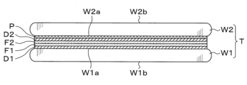
- a wafer processing system 1 In a wafer processing system 1 according to the present embodiment, which will be described later, as shown in FIG. 1, processing is performed on a stacked wafer T as a substrate in which a first wafer W1 and a second wafer W2 are bonded.
- the first wafer W1 the surface to be joined to the second wafer W2 will be referred to as the front surface W1a
- the surface opposite to the front surface W1a will be referred to as the back surface W1b.
- the surface to be bonded to the first wafer W1 is referred to as a front surface W2a
- the surface opposite to the front surface W2a is referred to as a back surface W2b.
- the first wafer W1 as the lower substrate is, for example, a semiconductor wafer such as a silicon substrate.
- the first wafer W1 has a substantially disk shape.
- a device layer D1 and a surface film F1 are laminated in this order from the front surface W1a side.
- Device layer D1 includes multiple devices.
- the surface film F1 include an oxide film (THOX film, SiO 2 film, TEOS film), SiC film, SiCN film, adhesive, and the like.
- the second wafer W2 as the upper substrate is also a semiconductor wafer such as a silicon substrate.
- the second wafer W2 has a substantially disk shape.
- a laser absorption layer P, a device layer D2, and a surface film F2 are laminated in this order from the front surface W2a side.
- the laser absorption layer P absorbs laser light irradiated from the laser irradiation section 110 as described later.
- an oxide film SiO 2 film
- the device layer D2 and the surface film F2 are similar to the device layer D1 and the surface film F1 of the first wafer W1, respectively.
- the wafer processing system 1 has a configuration in which a loading/unloading block 10, a transport block 20, and a processing block 30 are integrally connected.
- the loading/unloading block 10 and the processing block 30 are provided around the transport block 20.
- the carry-in/out block 10 is arranged on the Y-axis negative direction side of the conveyance block 20.
- a laser irradiation device 31 (described later) and a separation device 32 (described later) of the processing block 30 are located on the negative side of the X-axis of the transport block 20, and a first cleaning device 33 (described later) and a second cleaning device 34 (described later) are located on the X-axis negative side of the transport block 20.
- a reversing device 35 which will be described later, is arranged on the positive side of the X-axis and on the positive side of the Y-axis of the transport block 20, respectively.
- cassettes Ct, Cw1, and Cw2 each capable of accommodating a plurality of stacked wafers T, a plurality of first wafers W1, and a plurality of second wafers W2 are carried in and out of the carry-in/out block 10, respectively.
- the loading/unloading block 10 is provided with a cassette mounting table 11 .
- a plurality of cassettes for example, three cassettes Ct, Cw1, and Cw2, can be placed on the cassette mounting table 11 in a line in the X-axis direction. Note that the number of cassettes Ct, Cw1, and Cw2 placed on the cassette mounting table 11 is not limited to this embodiment, and can be arbitrarily determined.
- the three transport arms 23a to 23c are stacked in this order from above.
- the transport arms 23a to 23c are configured to be independently rotatable around vertical axes.
- a plurality of guide pins 25, for example three, are provided on the wafer holding surface of at least one of the three transfer arms 23a to 23c (the middle transfer arm 23b in the illustrated example).
- the guide pins 25 are arranged so as to surround the periphery of the stacked wafer T when the stacked wafer T is held by the transfer arm 23b.
- the guide pins 25 prevent the second wafer W2 from falling from above the first wafer W1 due to inertia or the like accompanying the transport of the stacked wafers T by the wafer transport device 22, as will be described later.
- the laser irradiation device 31 irradiates the inside of the polymerized wafer T, more specifically, the laser absorption layer P of the second wafer W2, with a laser beam to increase the bonding strength at the interface between the second wafer W2 and the laser absorption layer P. lower.
- the interface in this embodiment, the interface between the second wafer W2 and the laser absorption layer P
- the bonding strength is reduced inside the polymerized wafer T may be referred to as a "separation surface" in the technology of the present disclosure.
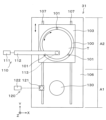
- a delivery position A1 and a processing position A2 are set inside the laser irradiation device 31.
- the transfer position A1 is a position where a wafer can be transferred between the transport arm 23 and a chuck 100, which will be described later, and a position where an image of the outer end of the stacked wafer T can be captured by an imaging mechanism 120, which will be described later.
- the processing position A2 is a position where the polymerized wafer T (laser absorption layer P) can be irradiated with laser light from a laser irradiation unit 110, which will be described later.
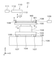
- the laser irradiation device 31 has a chuck 100 as a substrate holder that holds the superposed wafer T on its upper surface.
- the chuck 100 has a wafer holding surface on its upper surface, and holds the entire back surface W1b of the first wafer W1 by suction or a part of the radially inner side of the back surface W1b.
- the chuck 100 is, for example, an electrostatic chuck (ESC) or a vacuum chuck.
- the chuck 100 is provided with a lifting pin 100a (see FIG. 16) for supporting the stacked wafer T from below and lifting it up and down.
- the elevating pin 100a is inserted through a through hole (see FIG. 16) formed through the chuck 100, and is configured to be able to move up and down.
- the chuck 100 is provided with a plurality of, for example three, wafer fall prevention pins 101 as substrate fall prevention pins so as to surround the stacked wafer T on the holding surface along the radial direction.
- the wafer fall prevention pin 101 prevents the second wafer W2 from unintentionally separating from the first wafer W1 during or after laser beam irradiation due to, for example, centrifugal force accompanying the rotation of the chuck 100 or inertia force associated with movement. This prevents the second wafer W2 from falling from above the first wafer W1 when the second wafer W2 separates.
- the wafer fall prevention pin 101 is not particularly limited.
- the wafer fall prevention pin 101 is configured to be rotatable together with the chuck 100 by a rotation mechanism 104 described below, and movable in the Y-axis direction together with the chuck 100 by a drive mechanism 105 described later. Furthermore, it is configured to be able to move up and down in the Z-axis direction integrally with the above-mentioned lifting pin 100a.
- the chuck 100 is supported by a slider table 103 via an air bearing 102.
- a rotation mechanism 104 is provided on the lower surface side of the slider table 103.
- the rotation mechanism 104 has a built-in motor as a drive source, for example.
- the chuck 100 is configured to be rotatable around the ⁇ axis (vertical axis) by a rotation mechanism 104 via an air bearing 102 .
- the slider table 103 is movable between the above-mentioned delivery position A1 and processing position A2 by a drive mechanism 105 provided on the lower surface of the slider table 103 along a rail 107 provided on the base 106 and extending in the Y-axis direction. It is configured.
- the drive source of the drive mechanism 105 is not particularly limited, but a linear motor may be used, for example.
- the laser head 111 includes a laser oscillator (not shown) that oscillates laser light in a pulsed manner.
- This laser light is a so-called pulsed laser.
- the laser beam is a CO 2 laser beam, and the wavelength of the CO 2 laser beam is, for example, 8.9 ⁇ m to 11 ⁇ m.
- the laser head 111 may include equipment other than the laser oscillator, such as an amplifier.
- the lens 113 irradiates the polymerized wafer T held by the chuck 100 with laser light.
- the laser light emitted from the laser irradiation section 110 passes through the second wafer W2 and is irradiated onto the laser absorption layer P.
- the lens 113 may be configured to be movable up and down by a lifting mechanism (not shown).
- an imaging mechanism 120 as a detection mechanism is provided above the chuck 100 at the delivery position A1.
- the imaging mechanism 120 includes, for example, one or more cameras 121 selected from a macro camera, a micro camera, etc., and a calculation unit 122.
- the imaging mechanism 120 may be configured to be movable in the Y-axis direction and the Z-axis direction by a lifting mechanism (not shown) or a moving mechanism (not shown).
- a camera 121 serving as an acquisition unit images the outer end of the stacked wafer T held by the chuck 100.
- the camera 121 includes, for example, a coaxial lens, emits infrared light (IR), and receives reflected light from an object. Then, the camera 121 acquires position information of the stacked wafer T (at least the second wafer W2) on the chuck 100 by imaging the outer end of the stacked wafer T in this manner.
- the calculation unit 122 as a determination unit calculates the amount of eccentricity (horizontal direction (the amount of deviation with respect to the direction along the separation plane: see FIG. 6) is detected. Details of how the imaging mechanism 120 detects the eccentricity of the first wafer W1 and the second wafer W2 will be described later. In FIG.
- the acquisition unit (camera 121 or length measurement sensor) according to the technology of the present disclosure is arranged above the chuck 100 at the delivery position A1.
- the acquisition unit may be placed on the side of the chuck 100.
- a transport pad 130 is further provided above the chuck 100 at the delivery position A1.
- the transport pad 130 is configured to be able to be raised and lowered by a lifting mechanism (not shown). Further, the transport pad 130 has a suction surface on the lower surface side for suctioning and holding the first wafer W1. Then, the transport pad 130 detects that the first wafer W1 and the second wafer W2 are eccentric in the polymerized wafer T after the laser absorption layer P is irradiated with the laser beam by the imaging mechanism 120 described above. In this case, the second wafer W2 is transferred between the chuck 100 and the transfer arm 23. Note that details of the operation of the transport pad 130 will be described later.
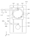
- the separation device 32 separates the second wafer W2 from the first wafer W1 based on the interface between the second wafer W2 and the laser absorption layer P, which serves as a separation plane and whose bonding strength has been reduced by the laser irradiation device 31. .
- the separation device 32 includes a suction chuck 200 that suction-holds the back surface W1b of the first wafer W1 from below, and a suction pad 210 that suction-holds the back surface W2b of the second wafer W2 from above. and has.
- the suction chuck 200 is also provided with a lifting pin 200a for supporting the first wafer W1 from below and lifting it up and down.
- the lifting pin 200a is inserted through a through hole formed through the suction chuck 200, and is configured to be able to move up and down.
- the suction pad 210 is raised to separate the second wafer W2 from the laser absorption layer P, with the suction pad 210 suction-holding the second wafer W2, as shown in FIG.
- the first cleaning device 33 cleans the front surface W1a side of the first wafer W1 separated by the separation device 32. For example, a brush is brought into contact with the laser absorption layer P on the front surface W1a side of the first wafer W1 to clean the laser absorption layer P. Note that a pressurized cleaning liquid may be used to clean the first wafer W1. Further, the first cleaning device 33 may be configured to clean the front surface W1a side of the first wafer W1 as well as the back surface W1b.
- the above wafer processing system 1 is provided with a control device 40 as a control mechanism.
- the control device 40 is, for example, a computer, and has a program storage section (not shown).
- the program storage unit stores a program for controlling the processing of the stacked wafers T in the wafer processing system 1.
- the program storage unit also stores programs for controlling the operations of drive systems such as the various processing devices and transport devices described above to realize wafer processing in the wafer processing system 1, which will be described later.
- the above program may be one that has been recorded on a computer-readable storage medium H, and may have been installed in the control device 40 from the storage medium H. Further, the storage medium H may be temporary or non-temporary.
- a cassette Ct containing a plurality of stacked wafers T is placed on the cassette mounting table 11 of the loading/unloading block 10.
- the outer ends of the stacked wafers T (first wafer W1 and second wafer W2) on the chuck 100 that are suction-held by the chuck 100 are imaged using the imaging mechanism 120 (step St2 in FIG. 9). Specifically, while rotating the chuck 100, an image of the outer end of the stacked wafer T (the first wafer W1 and the first wafer W1) on the chuck 100 is captured by the camera 121. The position information of the second wafer W2) is acquired. The imaging result by the camera 121 is output to the calculation unit 122.
- the calculation unit 122 calculates the amount of eccentricity (horizontal deviation) between the rotation center of the chuck 100 and the center of the stacked wafer T (first wafer W1 and/or second wafer W2) based on the image taken by the camera 121. amount) may be calculated. If eccentricity is observed between the rotation center of the chuck 100 and the center of the stacked wafer T, it is desirable to perform eccentricity correction control in consideration of the eccentricity amount calculated when irradiating the laser beam L to the laser absorption layer P, which will be described later.
- the calculated eccentricity between the rotation center of the chuck 100 and the center of the superposed wafer T (second wafer W2) may be output to the control device 40.
- the chuck 100 is moved to the processing position A2 by the drive mechanism 105. Subsequently, irradiation of the laser light L (CO 2 laser light) from the laser irradiation unit 110 to the laser absorption layer P, more specifically, to the interface between the laser absorption layer P and the second wafer W2 is started.
- L CO 2 laser light
- the rotation mechanism 104 rotates the stacked wafer T held on the chuck 100, and the drive mechanism 105 moves the stacked wafer T in the Y-axis direction, while the laser beam is emitted.
- Light L is irradiated in a pulsed manner. Then, the irradiation position of the laser beam L is moved from the outside in the radial direction to the inside of the laser absorption layer P, and as a result, the laser beam L is irradiated spirally in a plan view as shown in FIG.
- the irradiation position of the laser beam L will be from the outside in the radial direction. As it moves inward, more specifically, as it approaches the rotation center of the chuck 100, the circumferential speed of the polymerized wafer T at the irradiation position of the laser beam L decreases, so it is necessary to increase the rotational speed of the polymerized wafer T. There is.
- the second wafer W2 is not displaced (separated) in the horizontal direction due to the centrifugal force associated with the rotation of the chuck 100 or the inertial force associated with the movement, and the second wafer W2 is not displaced (separated) in the horizontal direction by the centrifugal force associated with the rotation of the chuck 100 or the inertial force associated with the movement of the chuck 100. It refers to the bonding strength that can appropriately separate the second wafer W2 from the first wafer W1.
- the irradiation position of the laser light L is scanned in the X-axis direction, and the drive mechanism 105 moves the chuck 100 (polymerized wafer T) in the Y-axis direction. (See FIG. 10).
- a chuck is used for irradiating the central region R1 with the laser beam L.
- the laser light L is concentrically irradiated onto the laser absorption layer P so as to surround the central region R1. More specifically, when irradiating the outer peripheral region R2 with the laser beam L, the chuck 100 (polymerized wafer T) is rotated and moved in the Y-axis direction as described above, so that the laser beam L is spirally formed.
- the spirally processed portion in the outer peripheral region R2 is shown with a broken line and the concentrically processed portion is shown with a dashed line for clarity of illustration, but in reality, the spirally processed portion and the concentrically processed portion are shown with dashed lines.
- the irradiation interval of the laser beam L in the portion is constant.
- a plurality of regions having different conditions for irradiation with the laser beam L may be generated.
- the rotation of the chuck 100 is stopped/restarted every time the irradiation conditions of the laser beam L are changed, in other words, the chuck 100 is stopped when the irradiation conditions of the laser beam L are changed. If the laser processing is performed in a state where the laser processing is stopped, the time required for laser processing increases because acceleration/deceleration related to stopping/resuming the rotation takes time.
- the laser irradiation device 31 when changing the irradiation conditions of the laser beam L during irradiation of the laser beam L to the outer peripheral region R2, the irradiation of the laser beam L to the polymerized wafer T and the chuck It is desirable to stop only the movement of chuck 100 in the horizontal direction and continue rotation of chuck 100. By continuing to rotate the chuck 100 when the irradiation conditions of the laser beam L are changed in this way, as in the example of the present application shown in FIG. The time involved can be shortened.
- the irradiation restart position of the laser beam L after changing the irradiation conditions is the same as the irradiation end position of the laser beam L before changing the irradiation conditions. It may be the same position as , or it may be a different position as long as at least the irradiation positions of the laser beams L do not overlap.
- the irradiation restart position and the irradiation end position of the laser beam L are the same, after changing the irradiation conditions of the laser beam L, the laser beam L is rotated until the irradiation end position comes directly under the irradiation of the laser beam L.
- the interval at which the laser beam L is irradiated can be controlled to be constant over the entire surface of the laser absorption layer P, and the separation between the second wafer W2 and the laser absorption layer P can be controlled uniformly within the wafer surface.
- the irradiation restart position and the irradiation end position of the laser beam L are different, after changing the irradiation conditions of the laser beam L, immediately irradiate the laser beam L at least at a position where the irradiation positions of the laser beam L do not overlap. resume. In this case, the waiting time until the start of irradiation with the laser beam L can be reduced, and the time required for laser processing can be further shortened.
- the drive mechanism 105 When the central region R1 and the outer peripheral region R2 are irradiated with the laser beam L and the bonding strength is reduced over the entire surface of the second wafer W2 and the laser absorption layer P, the drive mechanism 105 then moves the chuck 100 (polymerized wafer T) is moved to the delivery position A1.
- the outer end of the stacked wafer T held by the chuck 100 is imaged using the imaging mechanism 120 (step St5 in FIG. 9). Specifically, while rotating the chuck 100, an image of the outer end of the stacked wafer T (the first wafer W1 and the first wafer W1) on the chuck 100 is captured by the camera 121. The position information of the second wafer W2) is acquired. The imaging result by the camera 121 is output to the calculation unit 122. The calculation unit 122 calculates the eccentricity of the first wafer W1 and the second wafer W2 after being irradiated with the laser beam L (see FIG. 6) based on the position information obtained from the imaging result by the camera 121. The calculated eccentricity of the first wafer W1 and the second wafer W2 after irradiation with the laser beam L may be output to the control device 40.
- the control device 40 determines the eccentricity of the first wafer W1 and the second wafer W2 before being irradiated with the output laser beam L, and the eccentricity of the first wafer W1 and the second wafer W2 after being irradiated with the laser beam L.
- the difference with the amount of eccentricity is calculated, and based on the difference value, it is determined whether the second wafer W2 is separated from the first wafer W1 (step St6 in FIG. 9).
- the superposed wafer T in which the bonding strength between the second wafer W2 and the laser absorption layer P has decreased is transferred to the first separation device 32 provided outside the laser irradiation device 31.
- the wafer W1 and the second wafer W2 are separated.
- the bonding strength between the second wafer W2 and the laser absorption layer P is reduced by irradiation with the laser beam L, the inertia force when moving the second wafer W2 to the delivery position A1 by the drive mechanism 105 and the chuck 100 Due to the centrifugal force accompanying the rotation, the second wafer W2 may be separated from the laser absorption layer P (first wafer W1) before being transferred to the separation device 32.
- the second wafer W2 is separated before being transferred to the separation device 32 in this way, there is a risk that not only will it not be possible to properly transfer the polymerized wafer T to the separation device 32, but also that the second wafer W2 may not be properly transferred to the separation device 32. There is a risk of the W2 falling and causing problems.
- step St6 it is determined whether or not the second wafer W2 has been separated from the first wafer W1 before transporting the polymerized wafer T to the separation device 32. It can be determined whether This prevents the wafer transfer device 22 from attempting to transfer the superposed wafer T in which the second wafer W2 is separated from the first wafer W1 to the separation device 32, and the second wafer W2 is This reduces the risk of dropping the item.
- a plurality of at least three wafer fall prevention pins 101 are provided so as to surround the overlapping wafer T held by the chuck 100.
- the superimposed wafer T for which it was determined that the second wafer W2 is separated from the first wafer W1 in step St6, is first held by the transfer pad 130 by suction and holding the back surface W2b of the second wafer W2.
- the transfer pad 130 is raised to remove the second wafer W2 from above the first wafer W1 (step St7 in FIG. 9).
- the first wafer W1 on the chuck 100 is transferred to the transfer arm 23c of the wafer transfer device 22, and the first wafer W1 is transferred from the laser irradiation device 31 (step St8 in FIG. 9).
- the first wafer W1 carried out from the laser irradiation device 31 is then transferred to the cassette Cw1 of the cassette mounting table 11 by the wafer transfer device 22. Further, the second wafer W2 carried out from the laser irradiation device 31 is turned upside down in the reversing device 35, that is, with the surface separated from the first wafer W1 facing upward. Thereafter, the wafer is transported by the wafer transport device 22 to the cassette Cw2 on the cassette mounting table 11. At this time, the first wafer W1 and the second wafer W2 are cleaned in the first cleaning device 33 and the second cleaning device 34, respectively, after their separation side surfaces W1a and W2a are cleaned, respectively.
- the cassettes may be transported to the cassettes Cw1 and Cw2 on the cassette mounting table 11, respectively.
- the superposed wafer T for which it is determined in step St6 that the second wafer W2 is not separated from the first wafer W1 is transferred from the chuck 100 to the transfer arm 23b of the wafer transfer device 22, and is transferred to the laser irradiation device. 31 (step St10 in FIG. 9).
- the wafer fall prevention pins 101 arranged so as to surround the periphery of the stacked wafer T held on the chuck 100 are integrated with the lifting pins 100a. It is configured to be able to move up and down in the Z-axis direction.
- the stacked wafer T is supported from below by the lifting pin 100a and raised, and then the holding surface of the chuck 100 and the lower surface of the stacked wafer T (the first This is carried out by inserting the transfer arm 23b between the back surfaces W1b) of the wafers W1, and then lowering the stacked wafers T using the lifting pins 100a.
- the wafer drop prevention pins 101 can surround the stacked wafers T even when the lift pins 100a are rising. This makes it possible to suppress the second wafer W2 from falling during transfer from the chuck 100 to the transfer arm 23b.
- the periphery of the polymerized wafer T is A transport arm 23b having guide pins 25 arranged in a surrounding manner is used. As a result, even if the second wafer W2 is separated from the first wafer W1, the second wafer W2 is can be prevented from falling.
- the polymerized wafer T carried out from the laser irradiation device 31 is then transferred to the separation device 32 by the wafer transfer device 22.
- a suction chuck 200 suction-holds the back surface W1b of the first wafer W1
- a suction pad 210 suction-holds the back surface W2b of the second wafer W2.
- the suction pad 210 is raised to separate the first wafer W1 and the second wafer W2.
- the bonding strength at the interface between the laser absorption layer P and the second wafer W2 is reduced by the irradiation with the laser beam L, so the second wafer W2 can be separated without applying a large load. .
- the separated second wafer W2 is transferred from the suction pad 210 to the transfer arm 23a of the wafer transfer device 22, and then transferred to the reversing device 35, as shown in FIG. Then, after the surface W2a is turned upward in the reversing device 35, it is transported to the second cleaning device 34.
- the front surface W2a which is the side separated from the first wafer W1 is cleaned.
- the second cleaning device 34 may clean both the front surface W2a and the back surface W2b. Further, separate cleaning sections may be provided to clean the front surface W2a and the back surface W2b, respectively. Thereafter, the second wafer W2 that has been cleaned by the second cleaning device 34 is transferred to the cassette Cw2 of the cassette mounting table 11 by the wafer transfer device 22.
- the first wafer W1 held by the suction chuck 200 is transferred to the transfer arm 23c and transferred to the first cleaning device 33, as shown in FIG.
- This transfer by the transfer arm 23c may be performed simultaneously with the transfer of the second wafer W2 by the transfer arm 23a, or may be performed independently.
- the surface W1a side that is the side separated from the second wafer W2, specifically, the surface of the laser absorption layer P is cleaned.
- the back surface W1b of the first wafer W1 may be cleaned together with the front surface of the laser absorption layer P.
- separate cleaning sections may be provided to clean the front surface of the laser absorption layer P and the back surface W1b of the first wafer W1, respectively.
- the first wafer W1 that has been cleaned by the first cleaning device 33 is transferred to the cassette Cw1 of the cassette mounting table 11 by the wafer transfer device 22.
- the amount of eccentricity of the second wafer W2 with respect to the first wafer W1 before and after irradiation of the laser beam L to the polymerized wafer T (laser absorption layer P) Separation of the second wafer W2 was detected based on the difference value.
- the configuration of the second wafer W2 detection mechanism and the detection method using the same are not limited, and may include at least one of the following configurations and methods instead of or in addition to the above configurations and methods. Good too.
- the acceleration required to move the chuck 100 from the processing position A2 to the delivery position A1 after irradiation with the laser beam L is compared to the acceleration of the chuck 100 from the delivery position A1 to the processing position A2 before the irradiation with the laser beam
- the acceleration may be made larger than the acceleration required for movement of the superposed wafer T to apply an inertial force as a load.
- the magnitude of the load applied to the polymerized wafer T after irradiation with the laser beam L is such that the separated second wafer W2 can be shifted on the first wafer W1, and the second wafer W2 is If not separated, the size is controlled to such an extent that the second wafer W2 does not shift on the first wafer W1 (the second wafer W2 is not separated).
- the first wafer W1 and the second wafer W2 are intentionally eccentric (horizontal misalignment). bring about This makes it possible to avoid the situation where eccentricity does not occur even though the second wafer W2 is separated from the first wafer W1, as described above, and as a result, the second wafer The fear that W2 will fall from the first wafer W1 can be further appropriately suppressed.
- both the imaging mechanism 120 as a detection mechanism and the contact sensor 108 may be arranged in the laser irradiation device 31. In this case, both the detection of separation of the first wafer W1 and the second wafer W2 by the imaging mechanism 120 and the detection by the contact sensor 108 may be performed. In this case, when contact between the contact sensor 108 and the second wafer W2 is detected, the imaging mechanism 120 detects the separation of the first wafer W1 and the second wafer W2 (the outer edge of the superimposed wafer T imaging) may be omitted.
- the first wafers before and after irradiation with the laser beam L are obtained by imaging the outer ends of the stacked wafers T (the first wafer W1 and the second wafer W2) by the imaging mechanism 120. Separation of the second wafer W2 was detected based on the difference in eccentricity between the wafer W1 and the second wafer W2.
- the imaging mechanism 120 does not necessarily need to perform imaging of the outer ends of the stacked wafers T (the first wafer W1 and the second wafer W2) before and after the irradiation of the laser beam L, but only after the irradiation of the laser beam L. may be carried out.
- the first images before and after irradiation with the laser beam L are obtained by imaging the outer ends of the stacked wafers T (the first wafer W1 and the second wafer W2) using the imaging mechanism 120. Separation of the second wafer W2 was detected based on the difference in eccentricity between the wafer W1 and the second wafer W2.
- the imaging mechanism 120 may not be able to image the outer end of the first wafer W1 as the lower substrate on the chuck 100.
- the imaging mechanism 120 may image only the outer end of the second wafer W2 as the upper substrate.
- the position information of the second wafer W2 on the chuck 100 before and after the irradiation with the laser beam L is acquired from the imaging result by the imaging mechanism 120, and the position information of the second wafer W2 relative to the center of the chuck 100 before and after the irradiation with the laser beam L is acquired.
- the horizontal eccentricity (shift amount) of the center (more specifically, the rotation center) of the wafer W2 is detected.
- the difference between the amount of eccentricity of the center of the second wafer W2 with respect to the center of the chuck 100 before irradiation with the laser beam and the amount of eccentricity of the center of the second wafer W2 with respect to the center of the chuck 100 after irradiation with the laser beam is calculated.
- the imaging mechanism 120 images the outer ends of the stacked wafers T (the first wafer W1 and the second wafer W2) at 360 degrees in the circumferential direction.
- the eccentricity of the second wafer W2 was calculated, and separation of the second wafer W2 was detected.
- the imaging mechanism 120 does not necessarily need to image the outer ends of the stacked wafers T (the first wafer W1 and the second wafer W2) at 360 degrees in the circumferential direction; Separation of the second wafer W2 can also be detected by capturing images at two locations (for example, a point at the reference position in the circumferential direction of 0 degrees and a point at 90 degrees in the circumferential direction from the reference position).
- the second Separation of wafer W2 can be detected. Therefore, the time required for imaging the outer end portion by the imaging mechanism 120 after irradiation with the laser beam L can be shortened, and thereby the takt time required for processing in the laser irradiation device 31 can be reduced.
- the laser irradiation unit 110 irradiates the central region R1 and the outer peripheral region R2 with the laser beam L to reduce the bonding strength over the entire surface of the second wafer W2 and the laser absorption layer P.
- the bonding strength is reduced across the entire surface of the second wafer W2 and the laser absorption layer P, as described above, there is a risk that the second wafer W2 will fall due to the inertial force when the polymerized wafer T is transported. be.
- the irradiation of the laser beam L is stopped in at least a part of the interface between the second wafer W2 and the laser absorption layer P, and the irradiation of the laser beam L is stopped in at least a part of the interface between the second wafer W2 and the laser absorption layer P.
- the bonding strength between the second wafer W2 and the laser absorption layer P may be maintained in this region. More specifically, in the wafer processing system 1, as shown in FIG. 19, at the interface between the second wafer W2 and the laser absorption layer P, the outermost peripheral region R0 (in FIG. The bonding strength between the second wafer W2 and the laser absorption layer P is increased in the central region R3 (see FIG. 19(b)), which is set near the center position of the central region R1. It is also possible to form a region that does not reduce the
- the "acquisition unit" of the detection mechanism is a length measurement sensor (displacement sensor) instead of the camera 121 as described above. total) can be used.
- the transport arm 23b equipped with the guide pin 25 is used to transport the first wafer W1 and the second wafer W2, as in step St10.
- the first wafer W1 and the second wafer W2 may be unloaded from the laser irradiation device 31.
- the lifting speed of the stacked wafer T by the lifting pin 100a and the transport speed of the stacked wafer T by the wafer transport device 22 are set as normal. It is desirable to control the moving speed to be lower than the specified moving speed (when separation of the second wafer W2 is not detected in step St6).
- the wafer processing method of the present disclosure was applied when performing laser lift-off to separate the second wafer W2 from the laser absorption layer P.
- the technique according to the present disclosure in the polymerized wafer T in which the first wafer W1 and the second wafer W2 are bonded, at least a portion of the first wafer W1 and/or the second wafer W2 is transferred to the polymerized wafer T. It can be applied arbitrarily as long as it is separated from the
- a spectral interferometer is arranged in the laser irradiation device 31, and the interface between the first wafer W1 and the second wafer W2 (more specifically, the second wafer
- the second wafer W2 is separated from the first wafer W1. It may also be determined whether or not they are separated.
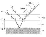
- a spectral interferometer 320 is arranged in a laser irradiation device 310 according to another embodiment.
- Spectroscopic interferometer 320 includes a head 321 and an analysis section 322.
- the head 321 includes an irradiation unit (not shown) that irradiates the overlapping wafer T on the chuck 100 with measurement light, and a irradiation unit (not shown) that irradiates the overlapping wafer T on the chuck 100 at different height positions (a first height position H1 and a second height position H2: FIG. and a spectroscopy unit (not shown) that receives the measurement light (reflected light) reflected by the laser beam (refer to FIG. 22) and detects interference between the reflected lights.
- a spectroscopy unit not shown
- As the measurement light irradiated from the irradiation section light that is transparent to the second wafer W (silicon) is arbitrarily selected.
- the central region R1 and the outer peripheral region R2 are irradiated with the laser beam L, and the bonding strength of the second wafer W2 and the laser absorption layer P is reduced over the entire surface of the stacked wafer T. 105 below the spectroscopic interferometer 320.
- the measurement light L2 from the irradiation part of the head 321 is irradiated toward the polymerized wafer T, and the reflected light from the polymerized wafer T enters the spectroscopic unit.
- the spectroscopy unit when interference of reflected light (reflection spectrum) is detected on the entire surface of the superposed wafer T, it is determined that the second wafer W2 is separated from the first wafer W1.
- the spectroscopic interferometer 320 may be moved and rotated relatively above the chuck 100 (polymerized wafer T). Furthermore, for example, by configuring the spectral interferometer 320 side by side with the laser irradiation device 310 or integrally with the laser irradiation device 310, the bonding strength reduction process by the laser irradiation device 310 and the separation determination by the spectral interferometer 320 can be performed simultaneously or sequentially. You may also do so.
- a more specific method of determining separation between the second wafer W2 and the first wafer W1 using the spectroscopic interferometer 320 will be described.
- the bonding strength at the interface between the second wafer W2 and the laser absorption layer P decreases due to irradiation with the laser beam L, and the second wafer W2 is separated from the first wafer W1, as shown in FIGS. 21 and 22.
- a space S which is a gap between the two, is formed.
- the analysis unit 322 calculates the thickness t of the space S (the first height position H1 and the second height position H2) based on this. Calculate the distance between The calculated thickness t of the space S is output to the control device 40.
- the control device 40 can determine whether the space S is formed at the interface between the second wafer W2 and the laser absorption layer P based on the output thickness t. When it is determined that the space S is formed over the entire surface of the polymerized wafer T (laser absorption layer P), the second wafer W2 and the laser absorption layer P have completely separated, and this means that the second wafer W2 and the laser absorption layer P have completely separated. It can be determined that wafer W2 is separated from first wafer W1.
- the calculated thickness t of the space S can be used as the value used as the first threshold value.
- the first threshold value is a value at which it is determined that the space S has been formed, and is a value greater than t>0, which is the thickness at which it is determined that the space S has been formed.
- the first threshold used for comparison may be set to a value greater than zero.
- the detection of reflected light from the polymerized wafer T using the spectroscopic interferometer 320 is performed using the polymerized wafer T (laser absorption layer P) in order to appropriately detect separation of the second wafer W2 from the first wafer W1. It is desirable that this be carried out across the board. However, for the purpose of shortening the time required for inspection and improving throughput, only a portion of the irradiation pitch of the laser beam L irradiated to the laser absorption layer P (for example, a portion of the radial direction or circumferential direction) is used. only).
- the spectroscopic interferometer 320 for detecting the separation of the first wafer W1 and the second wafer W2 is arranged inside the laser irradiation device 310 has been described as an example.
- the spectral interferometer 320 may be placed outside the laser irradiation device 310. That is, in the technology according to the present disclosure, the wafer processing system 1 includes a laser irradiation device 31 and an inspection device ( (not shown) may be arranged independently.
- the method of inspecting the separation state is not limited to this.
- this region may be at the same height as the optical flat. For example, it is determined that the space S is not formed.
- the space S which is the measurement result used for comparison with the first threshold in the above embodiment, is Instead of the thickness t, the amount of change t2 (see FIG. 22) in the height of the stacked wafer T that changes due to the formation of the space S can be used as the measurement result used for comparison with the first threshold value.
- a displacement meter (not shown) may be provided above the chuck 100, and the distance from the displacement meter to the back surface W2b of the second wafer W2 may be measured. good.
- the amount of change in the distance to the back surface W2b of the second wafer W2 before and after the formation of the space S, or the area where the distance to the back surface W2b and the bonding strength in the region where the space S is formed is not reduced.
- Separation of the first wafer W1 and the second wafer W2 may be determined by detecting the difference between the distance to the back surface W2b and the like (see FIG. 19).
- the device in the configuration of the laser irradiation device 310 shown in FIG. 20, the device can be configured only by changing the spectral interferometer 320 to a displacement meter (length measurement sensor) not shown.
- the laser beam L was sequentially irradiated to the preset central region R1 and outer peripheral region R2 (see FIG. 10) of the chuck 100.
- the determination as to whether or not to irradiate the central region R1 with the laser beam L may be made, for example, prior to irradiating the central region R1 with the laser beam L.
- the irradiation of the laser beam L to the central region R1 is continued. conduct.
- the overlapping wafer T in which the bonding strength between the second wafer W2 and the laser absorption layer P has decreased is then transferred to the separating device 32, where the first wafer W1 and the second wafer W2 are separated.
- the central region R1 is not irradiated with the laser beam L. Therefore, the bonding strength between the second wafer W2 and the laser absorption layer P is maintained in the central region R1.
- the polymerized wafer T is recovered from the laser irradiation device without being transported to the separation device 32. At this time, the polymerized wafer T may be collected into a cassette via a transport device, or may be removed from the laser irradiation device by manual collection by an operator.
- the second wafer W2 including the central region R1 and the laser absorption layer It is possible to suppress complete peeling of the entire surface of the interface between P and safely transport the polymerized wafer T without dropping the second wafer W2 within the laser irradiation device.
- the positional information of the peripheral region R2 is acquired prior to irradiating the peripheral region R2 with the laser beam L, and the positional information before the laser beam L is irradiated and the positional information after the laser beam L is irradiated are obtained.
- the state of peeling was determined by comparison with However, if the peeling state in the outer peripheral region R2 can be determined without comparing the positional information before and after irradiation with the laser beam L, it is not necessarily necessary to acquire the positional information before the irradiation with the laser beam L, and at least the laser beam to the central region R1 Before irradiating the light L, position information and the like may be acquired to check the peeling state.
- the laser absorption layer P, the device layer D2, and the surface film F2 are laminated in this order on the front surface W2a of the second wafer W2, and the interface between the laser absorption layer P and the second wafer W2 is
- the separation plane is set as the separation plane between the first wafer W1 and the second wafer W2
- the position of the separation plane is not limited thereto.
- a peeling process is performed between the second wafer W2 and the laser absorption layer P to promote peeling of the first wafer W1 and the second wafer W2.
- a promoting film (not shown) may be formed and the interface between the peel promoting film and the second wafer W2 may be set as a separation plane.
- the material constituting the peel-promoting film is such that the adhesion between the peel-promoting film and the second wafer W2 (silicon, etc.) It is desirable to select one that is at least smaller than the adhesion force between them.
Abstract
基板を処理する基板処理システムであって、前記基板を保持する保持面を有する基板保持部と、前記基板保持部を水平方向に移動させる駆動機構と、前記基板保持部を回転させる回転機構と、前記保持面に保持された前記基板に対しレーザ光を照射して、当該基板の分離の基点となる分離面を形成するレーザ照射部と、前記基板保持部に保持される前記基板において、前記分離面を基点とした分離を検知する検知機構と、を備える。
Description
本開示は、基板処理システム及び基板処理方法に関する。
特許文献1には、剥離酸化膜及び半導体素子が表面上に形成された半導体基板において、半導体素子を転写先基板に転写することが開示されている。特許文献1に記載の方法は、半導体基板の裏面より光を照射して剥離酸化膜を局所的に加熱する工程と、剥離酸化膜中、及び/又は剥離酸化膜と半導体基板との界面において剥離を生じさせて、半導体素子を転写先基板に転写させる工程と、を含む。
本開示にかかる技術は、レーザ光の照射により形成される分離面を基点として基板を分離する際に、レーザ光の照射後、基板の分離前に当該基板が分離されているか否かを適切に検知する。
本開示の一態様は、基板を処理する基板処理システムであって、前記基板を保持する保持面を有する基板保持部と、前記基板保持部を水平方向に移動させる駆動機構と、前記基板保持部を回転させる回転機構と、前記保持面に保持された前記基板に対しレーザ光を照射して、当該基板の分離の基点となる分離面を形成するレーザ照射部と、前記基板保持部に保持される前記基板において、前記分離面を基点とした分離を検知する検知機構と、を備える。
本開示によれば、レーザ光の照射により形成される分離面を基点として基板を分離する際に、レーザ光の照射後、基板の分離前に当該基板が分離されているか否かを適切に検知できる。
半導体デバイスの製造工程では、2枚の半導体基板(以下、「ウェハ」という。)が接合された重合ウェハにおいて、第2のウェハの表面に形成されたデバイス層を第1のウェハに転写することが行われている。このデバイス層の転写は、例えばレーザリフトオフを用いて実行される。すなわち、重合ウェハの内部にレーザ光を照射することで第1のウェハと第2のウェハの接合力を低下させた後、第2のウェハを第1のウェハから分離することで、デバイス層を第1のウェハに転写する。
このレーザリフトオフを行うためのウェハ処理システムでは、重合ウェハに対してレーザ光を照射するレーザ照射装置と、第1のウェハと第2のウェハを分離する分離装置と、が独立して構成される場合がある。ここで、レーザ照射装置におけるレーザ光の照射後には、第1のウェハと第2のウェハが意図せずに分離される場合が考えられる。この場合、第1のウェハと第2のウェハの水平方向の位置ズレを検知、抑制しないと、重合ウェハの搬送動作に伴う慣性力等により、第2のウェハが第1のウェハから落下してしまうおそれがある。
本開示にかかる技術は、上記事情に鑑みてなされたものであり、レーザ光の照射により形成される分離面を基点として基板を分離する際に、レーザ光の照射後、基板の分離前に当該基板が分離されているか否かを適切に検知する。なお、以下の説明において検知対象である基板の「分離」とは、第1のウェハに対して第2のウェハが水平方向に移動している状態を言うものとする。より具体的には、第1のウェハに対する第2のウェハの接合強度がゼロになり、第1のウェハに対して第2のウェハが独立して移動し得る状態と、第1のウェハと第2のウェハが未だ接合されているものの、接合強度が低下して第1のウェハに対して第2のウェハが水平方向にずれている状態と、を含むものとする。
以下、本実施形態にかかる基板処理システムとしてのウェハ処理システム、及び基板処理方法としてのウェハ処理方法ついて、図面を参照しながら説明する。なお、本明細書及び図面において、実質的に同一の機能構成を有する要素においては、同一の符号を付することにより重複説明を省略する。
本実施形態にかかる後述のウェハ処理システム1では、図1に示すように第1のウェハW1と第2のウェハW2とが接合された基板としての重合ウェハTに対して処理を行う。以下、第1のウェハW1において、第2のウェハW2に接合される側の面を表面W1aといい、表面W1aと反対側の面を裏面W1bという。同様に、第2のウェハW2において、第1のウェハW1に接合される側の面を表面W2aといい、表面W2aと反対側の面を裏面W2bという。
下側基板としての第1のウェハW1は、例えばシリコン基板等の半導体ウェハである。実施の形態において、第1のウェハW1は略円板形状を有する。第1のウェハW1の表面W1aには、デバイス層D1と表面膜F1が表面W1a側からこの順で積層されている。デバイス層D1は、複数のデバイスを含む。表面膜F1としては、例えば酸化膜(THOX膜、SiO2膜、TEOS膜)、SiC膜、SiCN膜又は接着剤などが挙げられる。
上側基板としての第2のウェハW2も、例えばシリコン基板等の半導体ウェハである。実施の形態において、第2のウェハW2は略円板形状を有する。第2のウェハW2の表面W2aには、レーザ吸収層P、デバイス層D2及び表面膜F2が表面W2a側からこの順で積層されている。レーザ吸収層Pは、後述するようにレーザ照射部110から照射されたレーザ光を吸収する。レーザ吸収層Pには、例えば酸化膜(SiO2膜)が用いられるが、レーザ光を吸収するものであれば特に限定されない。デバイス層D2と表面膜F2はそれぞれ、第1のウェハW1のデバイス層D1、表面膜F1と同様である。そして、第1のウェハW1の表面膜F1と第2のウェハW2の表面膜F2が接合される。なお、レーザ吸収層Pの位置は、上記実施形態に限定されず、例えばデバイス層D2と表面膜F2の間に形成されていてもよい。
図2に示すようにウェハ処理システム1は、搬入出ブロック10、搬送ブロック20、及び処理ブロック30を一体に接続した構成を有している。搬入出ブロック10と処理ブロック30は、搬送ブロック20の周囲に設けられている。具体的に搬入出ブロック10は、搬送ブロック20のY軸負方向側に配置されている。処理ブロック30の後述するレーザ照射装置31及び後述する分離装置32は搬送ブロック20のX軸負方向側に、後述する第1の洗浄装置33及び後述する第2の洗浄装置34は搬送ブロック20のX軸正方向側に、後述する反転装置35は搬送ブロック20のY軸正方向側に、それぞれ配置されている。
搬入出ブロック10は、例えば外部との間で複数の重合ウェハT、複数の第1のウェハW1、複数の第2のウェハW2をそれぞれ収容可能なカセットCt、Cw1、Cw2がそれぞれ搬入出される。搬入出ブロック10には、カセット載置台11が設けられている。図示の例では、カセット載置台11には、複数、例えば3つのカセットCt、Cw1、Cw2をX軸方向に一列に載置可能になっている。なお、カセット載置台11に載置されるカセットCt、Cw1、Cw2の個数は、本実施形態に限定されず、任意に決定することができる。
搬送ブロック20には、Y軸方向に延伸する搬送路21上を移動自在に構成された基板搬送機構としてのウェハ搬送装置22が設けられている。ウェハ搬送装置22は、重合ウェハT、第1のウェハW1又は第2のウェハW2を保持して搬送する、複数、例えば3つの搬送アーム23a~23c(以下の説明において、これらを併せて単に「搬送アーム23」という場合がある。)を有している。各搬送アーム23は、重合ウェハT、第1のウェハW1又は第2のウェハW2を吸着保持するための吸着部24(図3を参照)を、保持面に有する。各搬送アーム23は、水平方向、鉛直方向、水平軸回り及び鉛直軸回りに移動自在に構成されている。そして、ウェハ搬送装置22は、カセット載置台11のカセットCt、Cw1、Cw2、レーザ照射装置31、分離装置32、第1の洗浄装置33、第2の洗浄装置34及び反転装置35に対して、重合ウェハT、第1のウェハW1、第2のウェハW2を搬送可能に構成されている。
図3に示すように、3つの搬送アーム23a~23cは、上方からこの順に積層して配置されている。搬送アーム23a~23cはそれぞれ独立して鉛直軸回りに回転自在に構成されている。
3つの搬送アーム23a~23cのうち、少なくともいずれかひとつ(図示の例では中段の搬送アーム23b)のウェハ保持面には、複数、例えば3つのガイドピン25が設けられている。ガイドピン25は、搬送アーム23bによる重合ウェハTの保持時において、当該重合ウェハTの周囲を囲むように配置されている。そしてガイドピン25は、ウェハ搬送装置22による重合ウェハTの搬送に伴う慣性力等により、後述するように第2のウェハW2が第1のウェハW1上から落下することを抑制する。
また図3に示すように複数の搬送アーム23a~23cのうち、少なくともいずれかひとつ(図示の例では最上段の搬送アーム23a)は、重合ウェハT、第1のウェハW1又は第2のウェハW2を吸着保持するための吸着部24、すなわち保持面を下面側に有する。そして吸着部24を下面側に有する当該搬送アーム23aは、後述の分離装置32からの第2のウェハW2(上側基板)の搬出に際して、当該第2のウェハW2を上側から吸着保持する。
なお、搬送アーム23の構成は本実施形態に限定されず、任意の構成を取り得る。
処理ブロック30は、レーザ照射装置31、分離装置32、第1の洗浄装置33、第2の洗浄装置34及び反転装置35を有している。なお、レーザ照射装置31、分離装置32、第1の洗浄装置33、第2の洗浄装置34及び反転装置35の数や配置はこれに限定されるものではない。
レーザ照射装置31は、重合ウェハTの内部、より具体的には第2のウェハW2のレーザ吸収層Pにレーザ光を照射して第2のウェハW2とレーザ吸収層Pの界面における接合強度を低下させる。この重合ウェハTの内部において接合強度が低下した界面(本実施形態においては第2のウェハW2とレーザ吸収層Pの界面)を、本開示の技術においては「分離面」という場合がある。
図4及び図5に示すようにレーザ照射装置31の内部には受渡位置A1と処理位置A2が設定されている。受渡位置A1は、搬送アーム23と後述のチャック100との間でウェハの受け渡しができる位置であって、且つ、後述の撮像機構120により重合ウェハTの外端部を撮像できる位置である。処理位置A2は、後述のレーザ照射部110から重合ウェハT(レーザ吸収層P)にレーザ光を照射できる位置である。
レーザ照射装置31は、重合ウェハTを上面で保持する、基板保持部としてのチャック100を有している。チャック100は上面にウェハの保持面を備え、第1のウェハW1の裏面W1bの全面、又は裏面W1bの径方向内側の一部を吸着保持する。チャック100は、一例として静電チャック(ESC:Electrostatic Chuck)や真空チャック(Vacuum Chuck)である。
またチャック100には、重合ウェハTを下方から支持し昇降させるための昇降ピン100a(図16を参照)が設けられている。昇降ピン100aは、チャック100を貫通して形成された貫通孔(図16を参照)を挿通し、昇降自在に構成されている。
更にチャック100には、径方向に沿って保持面上の重合ウェハTの周囲を囲むように、複数、例えば3本の基板落下防止用ピンとしてのウェハ落下防止ピン101が設けられている。
ウェハ落下防止ピン101は、例えばチャック100の回転に伴う遠心力や、移動に伴う慣性力等により、レーザ光の照射中、又は照射後に第2のウェハW2が第1のウェハW1から意図せずに分離してしまった場合に、第2のウェハW2が第1のウェハW1上から落下することを抑制する。
ウェハ落下防止ピン101は、例えばチャック100の回転に伴う遠心力や、移動に伴う慣性力等により、レーザ光の照射中、又は照射後に第2のウェハW2が第1のウェハW1から意図せずに分離してしまった場合に、第2のウェハW2が第1のウェハW1上から落下することを抑制する。
ウェハ落下防止ピン101の配置は特に限定されるものではない。一例として本実施形態では、ウェハ落下防止ピン101は後述の回転機構104によってチャック100と一体に回転可能に構成されるとともに、後述の駆動機構105によってチャック100と一体にY軸方向に移動可能に構成され、更に、上記した昇降ピン100aと一体にZ軸方向に昇降可能に構成される。
チャック100は、エアベアリング102を介して、スライダテーブル103に支持されている。スライダテーブル103の下面側には、回転機構104が設けられている。回転機構104は、駆動源として例えばモータを内蔵している。チャック100は、回転機構104によってエアベアリング102を介して、θ軸(鉛直軸)回りに回転自在に構成されている。スライダテーブル103は、その下面側に設けられた駆動機構105によって、基台106に設けられY軸方向に延伸するレール107に沿って、上記した受渡位置A1と処理位置A2の間で移動可能に構成されている。なお、駆動機構105の駆動源は特に限定されるものではないが、例えばリニアモータが用いられる。
処理位置A2におけるチャック100の上方には、レーザ照射部110が設けられている。レーザ照射部110は、レーザヘッド111、光学系112、及びレンズ113を含む。
レーザヘッド111は、レーザ光をパルス状に発振するレーザ発振器(図示せず)を有している。このレーザ光は、いわゆるパルスレーザである。また、本実施形態ではレーザ光はCO2レーザ光であり、CO2レーザ光の波長は例えば8.9μm~11μmである。なお、レーザヘッド111は、レーザ発振器の他の機器、例えば増幅器などを有していてもよい。
光学系112は、レーザ光の強度や位置を制御する光学素子(図示せず)と、レーザ光を減衰させて出力を調整するアッテネータ(図示せず)とを有している。また、光学系112は、レーザ光の分岐を制御可能に構成されてもよい。
レンズ113は、チャック100に保持された重合ウェハTにレーザ光を照射する。レーザ照射部110から発せられたレーザ光は第2のウェハW2を透過し、レーザ吸収層Pに照射される。レンズ113は、昇降機構(図示せず)によって昇降自在に構成されていてもよい。
また、受渡位置A1におけるチャック100の上方には、検知機構としての撮像機構120が設けられている。撮像機構120は、一例としてマクロカメラやマイクロカメラ等から選択される1つ以上のカメラ121と、算出部122を備える。なお、撮像機構120は、図示しない昇降機構や図示しない移動機構によって、Y軸方向及びZ軸方向に移動自在に構成されてもよい。
取得部としてのカメラ121は、チャック100に保持された重合ウェハTの外端部を撮像する。カメラ121は、例えば同軸レンズを備え、赤外光(IR)を照射し、さらに対象物からの反射光を受光する。そしてカメラ121は、このように重合ウェハTの外端部を撮像することで、チャック100上における重合ウェハT(少なくとも第2のウェハW2)の位置情報を取得する。
判定部としての算出部122は、カメラ121が撮像した画像データから取得された、少なくとも第2のウェハW2の位置情報に基づき、第1のウェハW1に対する第2のウェハW2の偏心量(水平方向(分離面に沿った方向)に対するズレ量:図6を参照)を検知する。撮像機構120による第1のウェハW1と第2のウェハW2の偏心の検知方法の詳細は後述する。
なお図6においては、第1のウェハW1と第2のウェハW2の偏心を明確に示すため、チャック100が上記したウェハ落下防止ピン101を備えず、また、第1のウェハW1と第2のウェハW2に生じる偏心を実際よりも大きく示している。
判定部としての算出部122は、カメラ121が撮像した画像データから取得された、少なくとも第2のウェハW2の位置情報に基づき、第1のウェハW1に対する第2のウェハW2の偏心量(水平方向(分離面に沿った方向)に対するズレ量:図6を参照)を検知する。撮像機構120による第1のウェハW1と第2のウェハW2の偏心の検知方法の詳細は後述する。
なお図6においては、第1のウェハW1と第2のウェハW2の偏心を明確に示すため、チャック100が上記したウェハ落下防止ピン101を備えず、また、第1のウェハW1と第2のウェハW2に生じる偏心を実際よりも大きく示している。
なお、算出部122はこのように撮像機構120に独立して設けられていてもよいが、後述する制御装置40に含まれていてもよい。また、カメラ121による撮像結果や、算出部122により算出された偏心は、制御装置40に出力されてもよい。換言すれば、制御装置40は、本開示の技術に係る取得部及び判定部として機能を有する場合がある。
なお、本実施形態においては、本開示の技術に係る検知機構の「取得部」が、少なくとも第2のウェハW2の外端部を撮像する「カメラ121」である場合を例に説明を行うが、チャック100上における第2のウェハW2の位置を少なくとも取得できるものであれば、取得部の構成はこれに限定されない。具体的には、例えば本開示の技術に係る検知機構の「取得部」は、少なくとも第2のウェハW2までの距離を測定することで当該第2のウェハW2の位置情報を取得する、測長センサ(変位計)であってもよい。
また、本実施形態においては、本開示の技術に係る取得部(カメラ121又は測長センサ)が受渡位置A1におけるチャック100の上方に配置される場合を例に説明を行うが、チャック100上における少なくとも第2のウェハW2の位置を取得できれば、取得部はチャック100の側方に配置されてもよい。
受渡位置A1におけるチャック100の上方には、搬送パッド130が更に設けられている。搬送パッド130は、昇降機構(図示せず)によって昇降自在に構成されている。また、搬送パッド130は、第1のウェハW1を吸着保持するための吸着面を下面側に有している。
そして、搬送パッド130は、上記した撮像機構120により、レーザ吸収層Pに対するレーザ光の照射後の重合ウェハTにおいて第1のウェハW1と第2のウェハW2に偏心が生じていると検知された場合に、チャック100と搬送アーム23との間で第2のウェハW2を搬送する。なお、搬送パッド130の動作の詳細については後述する。
そして、搬送パッド130は、上記した撮像機構120により、レーザ吸収層Pに対するレーザ光の照射後の重合ウェハTにおいて第1のウェハW1と第2のウェハW2に偏心が生じていると検知された場合に、チャック100と搬送アーム23との間で第2のウェハW2を搬送する。なお、搬送パッド130の動作の詳細については後述する。
分離装置32は、レーザ照射装置31で接合強度が低下された、分離面としての第2のウェハW2とレーザ吸収層Pの界面を基点として第1のウェハW1から第2のウェハW2を分離する。
一例において分離装置32は、図7に示すように、第1のウェハW1の裏面W1bを下方から吸着保持する吸着チャック200と、第2のウェハW2の裏面W2bを上方から吸着保持する吸着パッド210とを有する。また吸着チャック200には、第1のウェハW1を下方から支持し昇降させるための昇降ピン200aが設けられている。昇降ピン200aは、吸着チャック200を貫通して形成された貫通孔を挿通し、昇降自在に構成されている。分離装置32では、図7に示すように吸着パッド210が第2のウェハW2を吸着保持した状態で、当該吸着パッド210を上昇させて、レーザ吸収層Pから第2のウェハW2を分離する。
なお、分離装置32の構成はこれに限定されるものではなく、第1のウェハW1から第2のウェハW2を分離できれば、任意の構成をとることができる。
第1の洗浄装置33は、分離装置32で分離された第1のウェハW1の表面W1a側を洗浄する。例えば第1のウェハW1の表面W1a側のレーザ吸収層Pにブラシを当接させて、当該レーザ吸収層Pを洗浄する。なお、第1のウェハW1の洗浄には、加圧された洗浄液を用いてもよい。また、第1の洗浄装置33は、第1のウェハW1の表面W1a側と共に、裏面W1bを洗浄する構成を有していてもよい。
第2の洗浄装置34は、分離装置32で分離された第2のウェハW2の表面W2a側を洗浄する。例えば第2のウェハW2の表面W2aにブラシを当接させて、当該表面W2aを洗浄する。なお、第2のウェハW2の洗浄には、加圧された洗浄液を用いてもよい。また、第2の洗浄装置34は、第2のウェハW2の表面W2a側と共に、裏面W2bを洗浄する構成を有していてもよい。
なお、本実施形態においては、上記したように第1のウェハW1を洗浄する第1の洗浄装置33と第2のウェハW2を洗浄する第2の洗浄装置34をそれぞれ独立して配置したが、第1のウェハW1の洗浄と第2のウェハW2の洗浄は、同一の洗浄装置を用いて行われてもよい。
反転装置35は、分離装置32で分離された後の第2のウェハW2の上下面を反転させる。すなわち、分離後の第2のウェハW2において第1のウェハW1から分離された側の面である表面W2aが上側を向くように、第2のウェハW2の表裏面を反転させる。反転装置35の構成は特に限定されない。
以上のウェハ処理システム1には、制御機構としての制御装置40が設けられている。制御装置40は、例えばコンピュータであり、プログラム格納部(図示せず)を有している。プログラム格納部には、ウェハ処理システム1における重合ウェハTの処理を制御するプログラムが格納されている。また、プログラム格納部には、上述の各種処理装置や搬送装置などの駆動系の動作を制御して、ウェハ処理システム1における後述のウェハ処理を実現させるためのプログラムも格納されている。なお、上記プログラムは、コンピュータに読み取り可能な記憶媒体Hに記録されていたものであって、当該記憶媒体Hから制御装置40にインストールされたものであってもよい。また、上記記憶媒体Hは、一時的なものであっても非一時的なものであってもよい。
次に、以上のように構成されたウェハ処理システム1を用いて行われるウェハ処理について説明する。なお、本実施形態では、ウェハ処理システム1の外部の接合装置(図示せず)において、第1のウェハW1と第2のウェハW2が接合され、予め重合ウェハTが形成されている。
先ず、複数の重合ウェハTを収納したカセットCtが、搬入出ブロック10のカセット載置台11に載置される。
次に、ウェハ搬送装置22の搬送アーム23cによりカセットCt内の重合ウェハTが取り出され、レーザ照射装置31に搬送される。レーザ照射装置31では、図8に示すようにレーザ照射部110からレーザ吸収層P、より詳細にはレーザ吸収層Pと第2のウェハW2の界面にレーザ光L(CO2レーザ光)をパルス状に照射し、レーザ吸収層Pと第2のウェハW2の接合強度を低下させる。
レーザ照射装置31における具体的なウェハ処理方法について説明する。
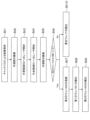
レーザ照射装置31において重合ウェハTは、搬送アーム23cから受渡位置A1に配置されたチャック100に受け渡され、チャック100に吸着保持される(図9のステップSt1)。
続いて、チャック100に吸着保持されたチャック100上の重合ウェハT(第1のウェハW1及び第2のウェハW2)の外端部を、撮像機構120を用いて撮像する(図9のステップSt2)。具体的には、チャック100を回転させながら、カメラ121によって重合ウェハTの周方向360度における外端部の画像が撮像され、これによりチャック100上における重合ウェハT(第1のウェハW1及び第2のウェハW2)の位置情報が取得される。カメラ121による撮像結果は、算出部122に出力される。
算出部122では、カメラ121による撮像結果から得られたチャック100上における第1のウェハW1と第2のウェハW2の位置情報に基づき、レーザ光Lの照射前の第1のウェハW1と第2のウェハW2の偏心量(図6を参照)を算出する。算出されたレーザ光Lの照射前の第1のウェハW1と第2のウェハW2の偏心量は、後述するレーザ光Lの照射後の第1のウェハW1と第2のウェハW2の偏心量との比較により、レーザ光Lの照射後に第1のウェハW1と第2のウェハW2にズレが生じているか、すなわち、第2のウェハW2が第1のウェハW1から分離されているか否かを判定するために用いられる。
算出されたレーザ光Lの照射前の第1のウェハW1と第2のウェハW2の偏心量は、制御装置40に出力されてもよい。
算出されたレーザ光Lの照射前の第1のウェハW1と第2のウェハW2の偏心量は、制御装置40に出力されてもよい。
また算出部122では、カメラ121による撮像結果に基づいて、チャック100の回転中心と重合ウェハT(第1のウェハW1及び/又は第2のウェハW2)の中心との偏心量(水平方向のズレ量)を算出してもよい。チャック100の回転中心と重合ウェハTの中心に偏心が見られる場合、後述のレーザ吸収層Pに対するレーザ光Lの照射に際して算出された当該偏心量を考慮し、偏心補正制御を行うことが望ましい。
算出されたチャック100の回転中心と重合ウェハT(第2のウェハW2)の中心の偏心量は、制御装置40に出力されてもよい。
算出されたチャック100の回転中心と重合ウェハT(第2のウェハW2)の中心の偏心量は、制御装置40に出力されてもよい。
また制御装置40では、予め設定された、後述のチャック100の中央領域R1及び外周領域R2(図10を参照)の位置を取得し、当該中央領域R1及び外周領域R2を、カメラ121による撮像結果に基づいてレーザ光Lの照射対象である重合ウェハTに対して設定する。より具体的には、チャック100に保持された重合ウェハTの面内において、中央領域R1と外周領域R2のそれぞれに対応する領域(平面視においてこれら中央領域R1と外周領域R2のそれぞれと重複する領域)を設定する。チャック100の中央領域R1及び外周領域R2の位置は、チャック100の回転中心を基準として設定され、制御装置40に予め出力されていたものを取得してもよい。
次に、駆動機構105によってチャック100を処理位置A2に移動させる。
続いて、レーザ照射部110からレーザ吸収層P、より詳細にはレーザ吸収層Pと第2のウェハW2の界面へのレーザ光L(CO2レーザ光)の照射を開始する。
続いて、レーザ照射部110からレーザ吸収層P、より詳細にはレーザ吸収層Pと第2のウェハW2の界面へのレーザ光L(CO2レーザ光)の照射を開始する。
ここで、本実施形態にかかるレーザ照射装置31では、回転機構104によってチャック100に保持された重合ウェハTを回転させると共に、駆動機構105によって当該重合ウェハTをY軸方向に移動させながら、レーザ光Lをパルス状に照射する。そうすると、レーザ光Lの照射位置はレーザ吸収層Pに対して径方向外側から内側に向けて移動され、その結果、レーザ光Lは図10に示すように平面視において螺旋状に照射される。
この際、第2のウェハW2とレーザ吸収層Pの分離をウェハ面内で均一に行うため、レーザ光Lを照射する間隔を一定にしようとすると、レーザ光Lの照射位置が径方向外側から内側に移動するにしたがって、より具体的にはチャック100の回転中心に近づくにしたがって、レーザ光Lの照射位置における重合ウェハTの周速が遅くなるため、重合ウェハTの回転速度を速くする必要がある。しかしながら、このように重合ウェハTの回転速度を速くした場合、レーザ光Lの照射途中であっても、重合ウェハTの回転に伴う遠心力により第2のウェハW2が第1のウェハW1から予期せずに分離してしまうおそれがある。
そこで本実施形態においては、重合ウェハTの周速が比較的早い上記したチャック100の外周領域R2(図10を参照)に対するレーザ光Lの照射においては重合ウェハTを回転させ、重合ウェハTの周速が遅くなるチャック100の中央領域R1(図10を参照)に対するレーザ光Lの照射においては重合ウェハTの回転を停止させた状態でレーザ光Lを走査させる。
なお、レーザ光Lを走査させるチャック100の中央領域R1は、チャック100の回転中心を基準として所望の径長を有する円形状領域として、上記したように、レーザ照射装置31におけるウェハ処理に先立って予め設定されている。中央領域R1の径長は、例えばレーザ照射部110のレンズ113に対するチャック100の相対的な回転速度が上限に達する径方向位置であり、換言すれば、レーザ光Lが重ならない限界の位置である。中央領域R1の径長は、一例として10mm程度である。
また、レーザ光Lの照射に際してチャック100を回転させる外周領域R2は、中央領域R1よりも径方向外側の領域に設定されている。
また、レーザ光Lの照射に際してチャック100を回転させる外周領域R2は、中央領域R1よりも径方向外側の領域に設定されている。
レーザ吸収層Pへのレーザ光Lの照射に際しては、先ず、この外周領域R2と対応する領域における重合ウェハT(レーザ吸収層P)に対してレーザ光Lを照射する(図9のステップSt3)。この時、レーザ照射装置31では、上記したようにレーザ照射部110からレーザ光Lをパルス状に照射させながら、チャック100(重合ウェハT)を回転させるとともに、チャック100(重合ウェハT)をY軸方向へ移動させることで、図10に示したように、径方向外側から内側に向けて螺旋状にレーザ光Lを照射する。この際、レーザ光Lは、図8に示したように第2のウェハW2の裏面W2b側(保持面とは反対側)から照射されて当該第2のウェハW2を透過し、レーザ吸収層Pにおいて吸収される。これによりレーザ吸収層Pと第2のウェハW2との界面において接合強度が低下する。
なお、実施の形態において「接合強度が低下」とは、少なくともレーザ光Lの照射前と比較して接合強度が低下している状態のことを言う。より具体的には、チャック100の回転に伴う遠心力や移動に伴う慣性力によっては第2のウェハW2が水平方向にずれる(分離される)ことがなく、且つ、後述の分離装置32において第1のウェハW1から第2のウェハW2を適切に分離できる接合強度を言う。
なお、実施の形態において「接合強度が低下」とは、少なくともレーザ光Lの照射前と比較して接合強度が低下している状態のことを言う。より具体的には、チャック100の回転に伴う遠心力や移動に伴う慣性力によっては第2のウェハW2が水平方向にずれる(分離される)ことがなく、且つ、後述の分離装置32において第1のウェハW1から第2のウェハW2を適切に分離できる接合強度を言う。
外周領域R2と対応する領域へのレーザ光Lの照射(第2のウェハW2とレーザ吸収層Pの接合強度の低下)が完了すると、次に、中央領域R1と対応する領域における重合ウェハT(レーザ吸収層P)に対してレーザ光Lを照射する(図9のステップSt4)。中央領域R1と対応する領域へのレーザ光Lの照射に際しては、チャック100の回転を停止する。そして、レーザ照射部110からレーザ光Lをパルス状に照射させながら、当該レーザ光Lの照射位置のX軸方向への走査と、駆動機構105によるチャック100(重合ウェハT)のY軸方向への移動を交互に繰り返し実行する(図10を参照)。
なお、ウェハ処理のスループットを向上させるため、上記した光学系112によりレーザ光Lを分岐させ、レーザ吸収層Pの複数点に同時にレーザ光Lを照射してもよい。
また、図10に示した例では、中央領域R1と対応する領域に対するレーザ光Lの照射に際して、照射位置のX軸方向への走査とY軸方向への移動を交互に繰り返し実行したが、外周領域R2と対応する領域と同様に、レーザ光Lを螺旋状に照射してもよい。または、図示は省略するが、レーザ光Lを重合ウェハT(レーザ吸収層P)と同心円状に環状に照射してもよい。
また、図10に示した例では、中央領域R1と対応する領域に対するレーザ光Lの照射に際して、照射位置のX軸方向への走査とY軸方向への移動を交互に繰り返し実行したが、外周領域R2と対応する領域と同様に、レーザ光Lを螺旋状に照射してもよい。または、図示は省略するが、レーザ光Lを重合ウェハT(レーザ吸収層P)と同心円状に環状に照射してもよい。
ここで、上記したように外周領域R2においてレーザ吸収層Pに対してレーザ光Lを螺旋状に照射した場合、図11に示すように、外周領域R2と中央領域R1の境界部近傍において、最大で周方向1周分程度のレーザ光Lの未照射領域が生じる。そして、このようにレーザ吸収層Pの面内にレーザ光Lの未照射領域が生じている場合、分離装置32において、当該未照射領域と対応する部分で適切にレーザ吸収層Pと第2のウェハW2を分離できないおそれがある。
そこで本実施形態に係るレーザ照射装置31においては、外周領域R2から中央領域R1へとレーザ光Lの照射を切り替えるに先立って、換言すれば、中央領域R1に対するレーザ光Lの照射のためにチャック100の回転を停止するに先立って、図12に示すように、レーザ吸収層Pに対して中央領域R1の周囲を囲むようにレーザ光Lを同心円状に照射する。
より具体的には、外周領域R2へのレーザ光Lの照射に際しては、上記したようにチャック100(重合ウェハT)を回転させると共に、Y軸方向に移動させることでレーザ光Lを螺旋状に照射したが、外周領域R2と中央領域R1の境界部の近傍においては、チャック100の(重合ウェハT)の回転を継続させつつ、Y軸方向への移動を停止させることで、レーザ吸収層Pに対してレーザ光Lを同心円状に照射する。
より具体的には、外周領域R2へのレーザ光Lの照射に際しては、上記したようにチャック100(重合ウェハT)を回転させると共に、Y軸方向に移動させることでレーザ光Lを螺旋状に照射したが、外周領域R2と中央領域R1の境界部の近傍においては、チャック100の(重合ウェハT)の回転を継続させつつ、Y軸方向への移動を停止させることで、レーザ吸収層Pに対してレーザ光Lを同心円状に照射する。
なお、レーザ吸収層Pに対するレーザ光Lの同心円状の照射は、図12に示したように中央領域R1の周囲において1周のみ行ってもよい。
又は、図13に示すように、レーザ照射部110からレーザ光Lをパルス状に照射させながら、回転機構104によるチャック100(重合ウェハT)の回転と、駆動機構105によるチャック100(重合ウェハT)のY軸方向への移動を交互に繰り返し実行することで、レーザ光Lの同心円状の照射を径方向に対して複数回行ってもよい。
更に、レーザ吸収層Pと第2のウェハW2とを適切に分離できれば、レーザ光Lの照射位置が重複することによりデバイス層に影響を与えることを抑制するため、図14に示すように、レーザ光Lの同心円状の照射を周方向に1周以下(図14の例では周方向270度)で止めるようにしてもよい。
又は、図13に示すように、レーザ照射部110からレーザ光Lをパルス状に照射させながら、回転機構104によるチャック100(重合ウェハT)の回転と、駆動機構105によるチャック100(重合ウェハT)のY軸方向への移動を交互に繰り返し実行することで、レーザ光Lの同心円状の照射を径方向に対して複数回行ってもよい。
更に、レーザ吸収層Pと第2のウェハW2とを適切に分離できれば、レーザ光Lの照射位置が重複することによりデバイス層に影響を与えることを抑制するため、図14に示すように、レーザ光Lの同心円状の照射を周方向に1周以下(図14の例では周方向270度)で止めるようにしてもよい。
そして、このようにレーザ光Lを外周領域R2と中央領域R1の境界部の近傍において同心円状に照射することで、レーザ吸収層Pに生じる未照射領域の大きさを小さくできるため、レーザ吸収層Pと第2のウェハW2の分離をより適切に行うことができる。
なお、図12、図13及び図14においては、図示の明瞭化のため外周領域R2における螺旋加工部分を破線、同心円加工部分を一点鎖線で示したが、実際には、螺旋加工部分と同心円加工部分におけるレーザ光Lの照射間隔は一定である。
なお、図10で示した例では、外周領域R2における径方向外側(レーザ吸収層Pの外端部近傍)から径方向内側(中央領域R1の境界部)へのレーザ光Lの照射を一度に行うかのように図示を行っている。しかしながら、実際には、この外周領域R2に対するレーザ光Lの照射途中であっても、レーザ光Lを照射する間隔を一定に制御するため、レーザ光Lの照射に係る条件、例えばレーザ光Lの周波数やチャック100の回転速度、チャック100の水平方向に対する移動速度等を変更する場合がある。
または、外周領域R2の中において、レーザ光Lの照射に係る条件が異なる複数の領域を生成する場合もある。
この時、図15の比較例に示すようにレーザ光Lの照射条件の変更毎にチャック100の回転を停止/再開させる場合、換言すればレーザ光Lの照射条件の変更をチャック100を停止させた状態で行う場合、この回転の停止/再開に係る加減速に時間を要するためにレーザ処理に係る時間が増加する。
または、外周領域R2の中において、レーザ光Lの照射に係る条件が異なる複数の領域を生成する場合もある。
この時、図15の比較例に示すようにレーザ光Lの照射条件の変更毎にチャック100の回転を停止/再開させる場合、換言すればレーザ光Lの照射条件の変更をチャック100を停止させた状態で行う場合、この回転の停止/再開に係る加減速に時間を要するためにレーザ処理に係る時間が増加する。
そこで本実施形態に係るレーザ照射装置31においては、外周領域R2に対するレーザ光Lの照射途中において当該レーザ光Lの照射条件を変更する場合には、重合ウェハTに対するレーザ光Lの照射、及びチャック100の水平方向に対する移動のみを停止させ、チャック100の回転は継続することが望ましい。
このようにレーザ光Lの照射条件の変更に際してチャック100の回転を継続することで、図15に示す本願例のように、チャック100の回転速度の加減速に係る時間を削減し、レーザ処理に係る時間を短縮できる。
このようにレーザ光Lの照射条件の変更に際してチャック100の回転を継続することで、図15に示す本願例のように、チャック100の回転速度の加減速に係る時間を削減し、レーザ処理に係る時間を短縮できる。
また、このようにチャック100の回転を継続してレーザ光Lの照射条件を変更する場合、照射条件変更後におけるレーザ光Lの照射再開位置は、照射条件変更前におけるレーザ光Lの照射終了位置と同じ位置であってもよいし、又は、少なくともレーザ光Lの照射位置が重複しなければ異なる位置であってもよい。
レーザ光Lの照射再開位置と照射終了位置を同じにする場合、レーザ光Lの照射条件の変更後、チャック100の回転によりレーザ光Lの照射直下に当該照射終了位置がくるまで、レーザ光Lの照射を再開しない。そしてこの場合、レーザ光Lを照射する間隔をレーザ吸収層Pの全面で一定に制御でき、第2のウェハW2とレーザ吸収層Pの分離をウェハ面内で均一に制御できる。
一方、レーザ光Lの照射再開位置と照射終了位置を異にする場合、レーザ光Lの照射条件の変更後、少なくともレーザ光Lの照射位置が重複しない位置で、速やかにレーザ光Lの照射を再開する。そしてこの場合、レーザ光Lの照射開始までの待ち時間を削減して、レーザ処理に係る時間を更に短縮できる。
中央領域R1及び外周領域R2にレーザ光Lが照射され、第2のウェハW2とレーザ吸収層Pの全面で接合強度が低下されると、次に、駆動機構105によってチャック100(重合ウェハT)を受渡位置A1に移動させる。
続いて受渡位置A1では、チャック100に吸着保持された重合ウェハTの外端部を、撮像機構120を用いて撮像する(図9のステップSt5)。具体的には、チャック100を回転させながら、カメラ121によって重合ウェハTの周方向360度における外端部の画像が撮像され、これによりチャック100上における重合ウェハT(第1のウェハW1及び第2のウェハW2)の位置情報が取得される。カメラ121による撮像結果は、算出部122に出力される。
算出部122では、カメラ121による撮像結果から得られた位置情報に基づき、レーザ光Lの照射後の第1のウェハW1と第2のウェハW2の偏心量(図6を参照)を算出する。算出されたレーザ光Lの照射後の第1のウェハW1と第2のウェハW2の偏心量は、制御装置40に出力されてもよい。
算出部122では、カメラ121による撮像結果から得られた位置情報に基づき、レーザ光Lの照射後の第1のウェハW1と第2のウェハW2の偏心量(図6を参照)を算出する。算出されたレーザ光Lの照射後の第1のウェハW1と第2のウェハW2の偏心量は、制御装置40に出力されてもよい。
制御装置40では、出力されたレーザ光Lの照射前の第1のウェハW1と第2のウェハW2の偏心量と、レーザ光Lの照射後の第1のウェハW1と第2のウェハW2の偏心量との差分を算出し、当該差分値に基づいて第2のウェハW2が第1のウェハW1から分離されているか否かを判定する(図9のステップSt6)。
本実施形態に係るウェハ処理システム1においては、第2のウェハW2とレーザ吸収層Pの接合強度が低下した重合ウェハTは、レーザ照射装置31の外部に設けられた分離装置32において、第1のウェハW1と第2のウェハW2の分離が行われる。
しかしながら上記したように、レーザ光Lの照射により第2のウェハW2とレーザ吸収層Pの接合強度を低下させた場合、駆動機構105によって受渡位置A1に移動される際の慣性力や、チャック100の回転に伴う遠心力により、分離装置32に搬送されるよりも前に第2のウェハW2がレーザ吸収層P(第1のウェハW1)から分離してしまう場合がある。
そして、このように分離装置32への搬送前に第2のウェハW2が分離した場合、分離装置32へ重合ウェハTを適切に搬送できなくなるおそれがあるのみならず、システム内で第2のウェハW2を落下させて支障を来たすおそれがある。
しかしながら上記したように、レーザ光Lの照射により第2のウェハW2とレーザ吸収層Pの接合強度を低下させた場合、駆動機構105によって受渡位置A1に移動される際の慣性力や、チャック100の回転に伴う遠心力により、分離装置32に搬送されるよりも前に第2のウェハW2がレーザ吸収層P(第1のウェハW1)から分離してしまう場合がある。
そして、このように分離装置32への搬送前に第2のウェハW2が分離した場合、分離装置32へ重合ウェハTを適切に搬送できなくなるおそれがあるのみならず、システム内で第2のウェハW2を落下させて支障を来たすおそれがある。
この点、本実施形態に係るレーザ照射装置31においては、ステップSt6において、分離装置32への重合ウェハTの搬送に先立って、第2のウェハW2が第1のウェハW1から分離しているか否かを判定できる。これにより、第2のウェハW2が第1のウェハW1から分離された状態の重合ウェハTをウェハ搬送装置22により分離装置32へ搬送しようとすることが抑制され、システム内で第2のウェハW2を落下させる懸念を低減できる。
また本実施形態においては、図4及び図5に示したように、チャック100に保持された重合ウェハTの周囲を囲むように、複数、少なくとも3本のウェハ落下防止ピン101を設けている。これにより、レーザ吸収層Pに対するレーザ光Lの照射後、第2のウェハW2が第1のウェハW1から分離した場合であっても、当該第2のウェハW2がレーザ照射装置31内で落下してしまうことが抑制される。
ステップSt6において第2のウェハW2が第1のウェハW1から分離していると判定された重合ウェハTは、先ず、搬送パッド130によって第2のウェハW2の裏面W2bを吸着保持した状態で、当該搬送パッド130を上昇させて、第1のウェハW1上から第2のウェハW2を退避させる(図9のステップSt7)。
次に、チャック100上の第1のウェハW1がウェハ搬送装置22の搬送アーム23cに受け渡され、当該第1のウェハW1がレーザ照射装置31から搬出される(図9のステップSt8)。この時、ステップSt2においてチャック100に対する第1のウェハW1の偏心(位置ズレ)が検知されている場合には、当該偏心量に合わせて、搬送アーム23cの挿入位置を調節してもよい。
更に続けて、搬送パッド130によって吸着保持した第2のウェハW2をウェハ搬送装置22の搬送アーム23aに受け渡し、当該第2のウェハW2をレーザ照射装置31から搬出する(図9のステップSt9)。この際、第2のウェハW2の裏面W2b(第1のウェハW1からの分離側とは反対面)を吸着保持するため、第2のウェハW2を上方から吸着して保持する搬送アーム23aが使用されることが望ましい。なお、第2のウェハW2はチャック100を介して搬送アーム23aに受け渡されてもよい。
レーザ照射装置31から搬出された第1のウェハW1は、その後、ウェハ搬送装置22によりカセット載置台11のカセットCw1に搬送される。また、レーザ照射装置31から搬出された第2のウェハW2は、反転装置35において上下面が反転された後、すなわち第1のウェハW1から分離された側の面が上方を向いた状態とされた後、ウェハ搬送装置22によりカセット載置台11のカセットCw2に搬送される。この際、第1のウェハW1及び第2のウェハW2は、それぞれ第1の洗浄装置33及び第2の洗浄装置34において、その分離側の面である表面W1a、表面W2aがそれぞれ洗浄された後にカセット載置台11のカセットCw1、Cw2にそれぞれ搬送されてもよい。
一方、ステップSt6において第2のウェハW2が第1のウェハW1から分離していないと判定された重合ウェハTは、チャック100からウェハ搬送装置22の搬送アーム23bへと受け渡され、レーザ照射装置31から搬出される(図9のステップSt10)。
ここで、上記したステップSt6において実際には第2のウェハW2が第1のウェハW1から分離されているにも拘らず、第2のウェハW2の分離を適切に検知できなかった場合、チャック100から搬送アーム23への受け渡しに際して重合ウェハTに加わる衝撃や、搬送アーム23による搬送に際しての慣性力等により、第2のウェハW2がシステム内で落下してしまうおそれがある。
この点、本実施形態に係るレーザ照射装置31においては、上記したように、チャック100に保持された重合ウェハTの周囲を囲むように配置されたウェハ落下防止ピン101を、昇降ピン100aと一体にZ軸方向に昇降可能に構成している。
チャック100からへの搬送アーム23bへの重合ウェハTの受け渡しは、昇降ピン100aにより重合ウェハTを下方から支持し、上昇させた後、チャック100の保持面と重合ウェハTの下面(第1のウェハW1の裏面W1b)の間に搬送アーム23bを挿入し、その後、昇降ピン100aにより重合ウェハTを降下させることにより行われる。
この時、図16に示すように、昇降ピン100aと一体にウェハ落下防止ピン101を昇降させることで、昇降ピン100aによる上昇時においても重合ウェハTの周囲をウェハ落下防止ピン101により囲むことができ、チャック100から搬送アーム23bへの受け渡しに際しての第2のウェハW2の落下を抑制できる。
また、本実施形態に係るウェハ処理システム1においては、レーザ照射装置31から分離装置32へレーザ光Lの照射後の重合ウェハTを搬送する際には、保持面上において重合ウェハTの周囲を囲むように配置されたガイドピン25を有する搬送アーム23bを使用する。
これにより、第2のウェハW2が第1のウェハW1から分離している場合であっても、レーザ照射装置31から分離装置32への重合ウェハTの搬送に際しての慣性力により第2のウェハW2が落下することを抑制できる。
これにより、第2のウェハW2が第1のウェハW1から分離している場合であっても、レーザ照射装置31から分離装置32への重合ウェハTの搬送に際しての慣性力により第2のウェハW2が落下することを抑制できる。
レーザ照射装置31から搬出された重合ウェハTは、続いて、ウェハ搬送装置22により分離装置32に搬送される。分離装置32では、図7に示したように、吸着チャック200で第1のウェハW1の裏面W1bを吸着保持し、更に吸着パッド210で第2のウェハW2の裏面W2bを吸着保持する。その後、吸着パッド210が第2のウェハW2を吸着保持した状態で、当該吸着パッド210を上昇させて、第1のウェハW1と第2のウェハW2を分離する。この際、上述したようにレーザ光Lの照射によってレーザ吸収層Pと第2のウェハW2の界面では接合強度が低下しているので、大きな荷重をかけることなく、第2のウェハW2を分離できる。
分離された第2のウェハW2は、図17に示すように、吸着パッド210からウェハ搬送装置22の搬送アーム23aに受け渡され、反転装置35に搬送される。そして、当該反転装置35において表面W2aが上側を向いた状態とされた後、第2の洗浄装置34に搬送される。
第2の洗浄装置34では、第1のウェハW1から分離された側の面である表面W2aが洗浄される。なお、第2の洗浄装置34では表面W2aと共に裏面W2bが洗浄されてもよい。また、表面W2aと裏面W2bをそれぞれ洗浄する洗浄部を別々に設けてもよい。
その後、第2の洗浄装置34による洗浄が施された第2のウェハW2は、ウェハ搬送装置22によりカセット載置台11のカセットCw2に搬送される。
第2の洗浄装置34では、第1のウェハW1から分離された側の面である表面W2aが洗浄される。なお、第2の洗浄装置34では表面W2aと共に裏面W2bが洗浄されてもよい。また、表面W2aと裏面W2bをそれぞれ洗浄する洗浄部を別々に設けてもよい。
その後、第2の洗浄装置34による洗浄が施された第2のウェハW2は、ウェハ搬送装置22によりカセット載置台11のカセットCw2に搬送される。
一方、吸着チャック200に保持されている第1のウェハW1については、図17に示したように搬送アーム23cに受け渡され、第1の洗浄装置33に搬送される。この搬送アーム23cによる搬送は、搬送アーム23aによる第2のウェハW2の搬送と同時に行われてもよいし、独立して行われてもよい。第1の洗浄装置33では、第2のウェハW2から分離された側の面である表面W1a側、具体的にはレーザ吸収層Pの表面が洗浄される。なお、第1の洗浄装置33では、レーザ吸収層Pの表面と共に、第1のウェハW1の裏面W1bが洗浄されてもよい。また、レーザ吸収層Pの表面と第1のウェハW1の裏面W1bをそれぞれ洗浄する洗浄部を別々に設けてもよい。
その後、第1の洗浄装置33による洗浄が施された第1のウェハW1は、ウェハ搬送装置22によりカセット載置台11のカセットCw1に搬送される。
その後、第1の洗浄装置33による洗浄が施された第1のウェハW1は、ウェハ搬送装置22によりカセット載置台11のカセットCw1に搬送される。
こうして、ウェハ処理システム1における一連のウェハ処理が終了する。
なお、以上の実施形態に係るレーザ照射装置31においては、上記したように重合ウェハT(レーザ吸収層P)に対するレーザ光Lの照射前後における第1のウェハW1に対する第2のウェハW2の偏心量の差分値に基づいて第2のウェハW2の分離を検知した。しかしながら、第2のウェハW2の検知機構の構成、及びこれを用いた検知方法は限定されず、上記構成、方法に代えて、又は加えて以下の少なくともいずれかの構成、方法を有していてもよい。
(1)上記したように、重合ウェハT(レーザ吸収層P)に対するレーザ光Lの照射後、実際には第2のウェハW2が第1のウェハW1から分離しているにも拘らず偏心(水平方向のズレ)が生じていない場合、第2のウェハW2の分離を適切に検知できない。
そこで、レーザ照射装置31における重合ウェハTに対するレーザ光Lの照射後、処理位置A2から受渡位置A1までのチャック100の移動に際して重合ウェハTに負荷をかけることで、第2のウェハW2を第1のウェハW1からずらす(第2のウェハW2を水平方向に移動させる)ようにしてもよい。より具体的には、例えばレーザ光Lの照射後の処理位置A2から受渡位置A1までのチャック100の移動にかかる加速度を、レーザ光Lの照射前の受渡位置A1から処理位置A2までのチャック100の移動にかかる加速度と比較して大きくし、重合ウェハTに負荷としての慣性力を与えてもよい。
この時、レーザ光Lの照射後の重合ウェハTにかける負荷の大きさは、分離された第2のウェハW2を第1のウェハW1上でずらすことができ、且つ、第2のウェハW2が分離していない場合には第1のウェハW1上で第2のウェハW2がずれない(第2のウェハW2が分離されない)程度の大きさに制御する。
上記方法(1)によれば、レーザ光Lの照射後の重合ウェハTに敢えて負荷をかけることで、第1のウェハW1と第2のウェハW2に意図的に偏心(水平方向のズレ)を生じさせる。これにより、上記したような第2のウェハW2が第1のウェハW1から分離しているにも拘らず偏心が生じていない状態を回避することができ、この結果、システム内において第2のウェハW2が第1のウェハW1から落下する懸念を更に適切に抑制できる。
また上記方法(1)によれば、このように第1のウェハW1と第2のウェハW2に意図的に偏心を生じさせることで、レーザ照射装置31での処理に係るタクトを軽減できる。
具体的に、上記方法(1)によれば、第1のウェハW1と第2のウェハW2に意図的に偏心を生じさせることで、重合ウェハTの周方向360度における外端部の撮像に代えて、外端部の少なくとも一部、例えば周方向の1箇所のみでエリア撮影することのみによって偏心を検知できる。このため、少なくとも重合ウェハT(レーザ吸収層P)に対するレーザ光Lの照射後の外端部の撮像に要する時間を省略でき、これによりタクトを軽減できる。
具体的に、上記方法(1)によれば、第1のウェハW1と第2のウェハW2に意図的に偏心を生じさせることで、重合ウェハTの周方向360度における外端部の撮像に代えて、外端部の少なくとも一部、例えば周方向の1箇所のみでエリア撮影することのみによって偏心を検知できる。このため、少なくとも重合ウェハT(レーザ吸収層P)に対するレーザ光Lの照射後の外端部の撮像に要する時間を省略でき、これによりタクトを軽減できる。
(2)レーザ照射装置31においては、図4及び図5に示したウェハ落下防止ピン101に代えて、又は加えて、図18に示すようにチャック100の保持面上の重合ウェハTの周囲を囲むように、複数、例えば3本の検知部としての接触式センサ108と、当該接触式センサ108による第2のウェハW2の分離を判定するための判定部としての算出部109と、を配置してもよい。この場合、上記実施形態に係る撮像機構120に代えて、又は加えて、これら接触式センサ108と算出部109が、本開示の技術に係る検知機構を構成する。
なお、算出部109は、レーザ照射装置31において独立して配置されてもよいし、制御装置40に含まれていてもよい。
なお、算出部109は、レーザ照射装置31において独立して配置されてもよいし、制御装置40に含まれていてもよい。
上記構成(2)によれば、重合ウェハT(レーザ吸収層P)に対するレーザ光Lの照射後における外端部の撮像に代えて、接触式センサ108と第2のウェハW2との接触の有無を判定することのみによって、第2のウェハW2の分離を検知できる。このため、重合ウェハT(レーザ吸収層P)に対するレーザ光Lの照射後における撮像機構120による外端部の撮像を省略でき、これによりレーザ照射装置31での処理に係るタクトを軽減できる。
なお、本開示の技術に係るウェハ処理システム1においては、検知機構としての撮像機構120と、接触式センサ108の両方をレーザ照射装置31に配置してもよい。この場合、撮像機構120による第1のウェハW1と第2のウェハW2の分離の検知と、接触式センサ108によるえと、の両方が行われてもよい。
またこの場合、接触式センサ108と第2のウェハW2の接触を検知した場合には、撮像機構120による第1のウェハW1と第2のウェハW2の分離の検知(重合ウェハTの外端部の撮像)は省略されてもよい。
またこの場合、接触式センサ108と第2のウェハW2の接触を検知した場合には、撮像機構120による第1のウェハW1と第2のウェハW2の分離の検知(重合ウェハTの外端部の撮像)は省略されてもよい。
(3)上記実施形態においては、撮像機構120により重合ウェハT(第1のウェハW1及び第2のウェハW2)の外端部を撮像して得られた、レーザ光Lの照射前後における第1のウェハW1と第2のウェハW2の偏心量の差分値に基づいて第2のウェハW2の分離を検知した。
しかしながら、撮像機構120による重合ウェハT(第1のウェハW1及び第2のウェハW2)の外端部の撮像は必ずしもレーザ光Lの照射前後に行われる必要はなく、レーザ光Lの照射後のみに行われてもよい。
しかしながら、撮像機構120による重合ウェハT(第1のウェハW1及び第2のウェハW2)の外端部の撮像は必ずしもレーザ光Lの照射前後に行われる必要はなく、レーザ光Lの照射後のみに行われてもよい。
上記方法(3)によっても、少なくともレーザ光Lの照射後における重合ウェハT(第1のウェハW1及び第2のウェハW2)の外端部を撮像し、第1のウェハW1と第2のウェハW2との偏心量(水平方向の位置ズレ量)を取得できれば、当該偏心量に基づいて第2のウェハW2の分離を判定できる。
(4)上記実施形態においては、撮像機構120により重合ウェハT(第1のウェハW1及び第2のウェハW2)の外端部を撮像して得られた、レーザ光Lの照射前後における第1のウェハW1と第2のウェハW2の偏心量の差分値に基づいて第2のウェハW2の分離を検知した。
しかしながら、例えば撮像機構120の画角や撮像倍率等の要因により、撮像機構120によっては、チャック100上における下側基板としての第1のウェハW1の外端部を撮像できない場合がある。
しかしながら、例えば撮像機構120の画角や撮像倍率等の要因により、撮像機構120によっては、チャック100上における下側基板としての第1のウェハW1の外端部を撮像できない場合がある。
そこで本開示の技術に係るウェハ処理システム1においては、撮像機構120により上側基板としての第2のウェハW2の外端部のみを撮像するようにしてもよい。
この場合、撮像機構120による撮像結果から、レーザ光Lの照射前後におけるチャック100上での第2のウェハW2の位置情報を取得し、レーザ光Lの照射前後におけるチャック100の中心に対する第2のウェハW2の中心(より具体的には回転中心)の水平方向の偏心量(ズレ量)を検知する。そして、レーザ光の照射前のチャック100の中心に対する第2のウェハW2の中心の偏心量と、レーザ光の照射後のチャック100の中心に対する第2のウェハW2の中心の偏心量と、の差分値を算出することで、当該差分値に基づいて第2のウェハW2の分離を判定できる。
この場合、撮像機構120による撮像結果から、レーザ光Lの照射前後におけるチャック100上での第2のウェハW2の位置情報を取得し、レーザ光Lの照射前後におけるチャック100の中心に対する第2のウェハW2の中心(より具体的には回転中心)の水平方向の偏心量(ズレ量)を検知する。そして、レーザ光の照射前のチャック100の中心に対する第2のウェハW2の中心の偏心量と、レーザ光の照射後のチャック100の中心に対する第2のウェハW2の中心の偏心量と、の差分値を算出することで、当該差分値に基づいて第2のウェハW2の分離を判定できる。
上記方法(4)によれば、撮像機構120により重合ウェハT(第1のウェハW1及び第2のウェハW2)の外端部を適切に撮像できない場合であっても、少なくとも第2のウェハW2の位置情報を取得することで、第2のウェハW2の分離を検知できる。
(5)上記実施形態においては、撮像機構120により重合ウェハT(第1のウェハW1及び第2のウェハW2)の外端部を周方向360度で撮像することで第1のウェハW1と第2のウェハW2の偏心量を算出し、第2のウェハW2の分離を検知した。
しかしながら、撮像機構120による重合ウェハT(第1のウェハW1及び第2のウェハW2)の外端部の撮像は必ずしも周方向360度で行われる必要はなく、少なくとも重合ウェハTの周方向の少なくとも2箇所(例えば周方向の基準位置0度の地点と、基準位置から周方向に90度の地点)を撮像することによっても、第2のウェハW2の分離を検知できる。
しかしながら、撮像機構120による重合ウェハT(第1のウェハW1及び第2のウェハW2)の外端部の撮像は必ずしも周方向360度で行われる必要はなく、少なくとも重合ウェハTの周方向の少なくとも2箇所(例えば周方向の基準位置0度の地点と、基準位置から周方向に90度の地点)を撮像することによっても、第2のウェハW2の分離を検知できる。
上記方法(5)によれば、重合ウェハTの外端部を周方向360度で撮像することに代え、重合ウェハTの外端部を周方向の2箇所でエリア撮影することによって第2のウェハW2の分離を検知できる。このため、レーザ光Lの照射後における撮像機構120による外端部の撮像時間を短縮でき、これによりレーザ照射装置31での処理に係るタクトを軽減できる。
(6)上記実施形態においては、レーザ照射部110により中央領域R1及び外周領域R2にレーザ光Lを照射し、第2のウェハW2とレーザ吸収層Pの全面で接合強度を低下させた。
しかしながら、このように第2のウェハW2とレーザ吸収層Pの全面で接合強度を低下させた場合、上記したように重合ウェハTの搬送に際しての慣性力により第2のウェハW2が落下するおそれがある。
しかしながら、このように第2のウェハW2とレーザ吸収層Pの全面で接合強度を低下させた場合、上記したように重合ウェハTの搬送に際しての慣性力により第2のウェハW2が落下するおそれがある。
そこで本開示の技術に係るウェハ処理システム1では、第2のウェハW2とレーザ吸収層Pの界面における少なくとも一部の領域でレーザ光Lの照射を停止させ、レーザ光Lを照射しない当該少なくとも一部の領域で、第2のウェハW2とレーザ吸収層Pの接合強度を維持するようにしてもよい。
より具体的にウェハ処理システム1では、図19に示すように、第2のウェハW2とレーザ吸収層Pの界面において、外周領域R2の最外周位置に設定される最外周領域R0(図19の(a)を参照)の一部や、中央領域R1の中心位置近傍に設定される中心領域R3(図19の(b)を参照)において、第2のウェハW2とレーザ吸収層Pの接合強度を低下させない領域を形成してもよい。
より具体的にウェハ処理システム1では、図19に示すように、第2のウェハW2とレーザ吸収層Pの界面において、外周領域R2の最外周位置に設定される最外周領域R0(図19の(a)を参照)の一部や、中央領域R1の中心位置近傍に設定される中心領域R3(図19の(b)を参照)において、第2のウェハW2とレーザ吸収層Pの接合強度を低下させない領域を形成してもよい。
上記方法(6)によれば、第2のウェハW2とレーザ吸収層Pの界面の少なくとも一部で接合強度を低下させない(レーザ光Lを照射しない)領域を形成することで、当該領域では第2のウェハW2が第1のウェハW1から分離されていないため、重合ウェハTに作用する慣性力等により第2のウェハW2が落下することを抑制できる。
本開示の技術に係るウェハ処理システム1においては、上記実施形態、上記方法(1)~上記方法(6)の少なくともいずれかにより、レーザ照射装置31からの重合ウェハTの搬出に先立って第2のウェハW2の分離を検知することで、システム内において第2のウェハW2が第1のウェハW1から落下する懸念を抑制できる。
また、このように上記方法(1)~上記方法(6)の少なくともいずれかを実行する場合においても、検知機構の「取得部」は、上記したようにカメラ121に代えて測長センサ(変位計)を使用できる。
なお、上記実施形態では、図9で示したようにステップSt6において第2のウェハW2の分離を検知した際に、第1のウェハW1と第2のウェハW2とを順次レーザ照射装置31から搬出(ステップSt8、ステップSt9)したが、分離を検知した際の動作はこれに限定されるものではない。
例えば、上記したように第1のウェハW1と第2のウェハW2を独立してレーザ照射装置31から搬出することに代え、ステップSt10と同様に、ガイドピン25を備える搬送アーム23bを用いて第1のウェハW1と第2のウェハW2を一体にレーザ照射装置31から搬出するようにしてもよい。この場合、第2のウェハW2が第1のウェハW1から落下することを抑制するため、昇降ピン100aによる重合ウェハTの昇降速度や、ウェハ搬送装置22による重合ウェハTの搬送速度は、通常時(ステップSt6で第2のウェハW2の分離が検知されなかった場合)の移動速度である規定速度よりも低速に制御することが望ましい。
また例えば、ステップSt6において第1のウェハW1と第2のウェハW2の分離が検知され、ウェハ搬送装置22による重合ウェハTの搬送が困難であると判定される場合には、制御装置40によりアラームを発報し、以降の処理を停止してもよい。またこの場合、重合ウェハTをオペレータの手回収によりレーザ照射装置31から除去するようにしてもよい。
また例えば、ステップSt6において第1のウェハW1と第2のウェハW2の分離が検知され、ウェハ搬送装置22による重合ウェハTの搬送が困難であると判定される場合には、制御装置40によりアラームを発報し、以降の処理を停止してもよい。またこの場合、重合ウェハTをオペレータの手回収によりレーザ照射装置31から除去するようにしてもよい。
なお、以上の実施形態では、レーザ吸収層Pから第2のウェハW2を分離するレーザリフトオフを行う際に、本開示のウェハ処理方法を適用した。しかしながら、本開示に係る技術は、第1のウェハW1と第2のウェハW2が接合された重合ウェハTにおいて、第1のウェハW1及び/又は第2のウェハW2の少なくとも一部を重合ウェハTから分離する場合であれば任意に適用できる。
例えば、半導体デバイスの製造工程においては、表面に複数の電子回路等のデバイスが形成されたウェハのシリコン基板の内部に、面方向に沿ってレーザ光を照射して改質層を形成し、当該改質層を分離面としてウェハを分離することで、ウェハを薄化することが行われている。このレーザ光には、YAGレーザ光が用いられる。このようにウェハの薄化の基点となる分離面としての改質層を形成する際にも、本開示技術を適用することができる。
また更に、本開示に係る技術は、第1のウェハW1と第2のウェハW2が接合された重合ウェハTにおいて、第1のウェハW1と第2のウェハW2を分離するデボンダー技術においても適用することができる。
また更に、本開示に係る技術は、第1のウェハW1と第2のウェハW2が接合された重合ウェハTにおいて、第1のウェハW1と第2のウェハW2を分離するデボンダー技術においても適用することができる。
なお、上記のようにシリコン基板の内部にレーザ光を照射して改質層を形成し、当該改質層を基点にウェハを分離する場合、レーザ照射装置31においては、上記実施形態に示した第1のウェハW1と第2のウェハW2との水平方向の位置ズレ量に代えて、チャック100に保持されて残置する下側ウェハと、分離により除去される対象の上側ウェハとの位置ズレを検知できればよい。
具体的に、例えば撮像機構120や測長センサに代えてレーザ照射装置31に分光干渉計を配置し、第1のウェハW1と第2のウェハW2の界面(より具体的には第2のウェハW2とレーザ吸収層Pの界面)に生じた空間を重合ウェハTの厚み方向(重合ウェハTの高さ方向の位置情報)で検知することで、第2のウェハW2が第1のウェハW1から分離されているか否かを判定してもよい。
図20に示すように、他の実施形態に係るレーザ照射装置310には、分光干渉計320が配置される。分光干渉計320は、ヘッド321と解析部322とを有する。
ヘッド321は、チャック100上の重合ウェハTに測定光を照射する図示しない照射部と、重合ウェハTの異なる高さ位置(第1の高さ位置H1及び第2の高さ位置H2:図21及び図22を参照)で反射した測定光(反射光)を受光して、当該反射光同士の干渉を検知する図示しない分光ユニットとを有する。照射部から照射される測定光としては、第2のウェハW(シリコン)に対して透過性を有する光が任意に選択される。
解析部322は、ヘッド321により検知される第1の高さ位置H1と第2の高さ位置H2のそれぞれからの反射光同士の干渉を検知することで、第1の高さ位置H1と第2の高さ位置H2の間の距離を算出する。なお、解析部322は制御装置40に組み込まれていてもよい。
続いて、分光干渉計320を用いて行われる、第2のウェハW2が第1のウェハW1から分離されているか否かの判定方法について説明する。
上記実施形態と同様の方法により、中央領域R1及び外周領域R2にレーザ光Lが照射され、第2のウェハW2とレーザ吸収層Pの全面で接合強度が低下された重合ウェハTは、駆動機構105によって分光干渉計320の下方に移動される。続いて、チャック100を回転させながら、図21に示すように、ヘッド321の照射部からの測定光L2を重合ウェハTに向けて照射するとともに、重合ウェハTからの反射光を分光ユニットに進入させる。分光ユニットでは、重合ウェハTの全面で反射光の干渉(反射スペクトル)を検知した場合、第2のウェハW2が第1のウェハW1から分離されていると判定する。
ただしこの時、上記実施形態で示したように、第2のウェハW2とレーザ吸収層Pの全面で接合強度が低下された重合ウェハTを保持したチャック100を移動、回転させると、第2のウェハW2が第1のウェハW1から落下するおそれがある。
かかる点に鑑みて、第2のウェハW2とレーザ吸収層Pの全面で接合強度が低下された重合ウェハTを保持したチャック100を移動、回転させる際には、この移動速度や回転速度を低下させることが望ましい。又は、チャック100を移動、回転させることに代えて、分光干渉計320をチャック100(重合ウェハT)の上方で相対的に移動、回転させるようにしてもよい。更に例えば、分光干渉計320をレーザ照射装置310と並べて、または一体に構成することで、レーザ照射装置310による接合強度の低下処理と、分光干渉計320による分離の判定を同時、または連続的に行うようにしてもよい。
かかる点に鑑みて、第2のウェハW2とレーザ吸収層Pの全面で接合強度が低下された重合ウェハTを保持したチャック100を移動、回転させる際には、この移動速度や回転速度を低下させることが望ましい。又は、チャック100を移動、回転させることに代えて、分光干渉計320をチャック100(重合ウェハT)の上方で相対的に移動、回転させるようにしてもよい。更に例えば、分光干渉計320をレーザ照射装置310と並べて、または一体に構成することで、レーザ照射装置310による接合強度の低下処理と、分光干渉計320による分離の判定を同時、または連続的に行うようにしてもよい。
分光干渉計320による第2のウェハW2と第1のウェハW1の分離判定のより具体的な判定方法について説明する。
レーザ光Lの照射により第2のウェハW2とレーザ吸収層Pの界面で接合強度が低下し、第2のウェハW2が第1のウェハW1から分離されている場合、図21及び図22で示したように、第2のウェハW2と第1のウェハW1の分離面(図示の例では第2のウェハW2とレーザ吸収層Pの界面)では、第2のウェハW2と第1のウェハW1の間の隙間である空間Sが形成されていると考えられる。
レーザ光Lの照射により第2のウェハW2とレーザ吸収層Pの界面で接合強度が低下し、第2のウェハW2が第1のウェハW1から分離されている場合、図21及び図22で示したように、第2のウェハW2と第1のウェハW1の分離面(図示の例では第2のウェハW2とレーザ吸収層Pの界面)では、第2のウェハW2と第1のウェハW1の間の隙間である空間Sが形成されていると考えられる。
そして、このように第2のウェハW2とレーザ吸収層Pの界面に空間Sが生じている場合、この空間の上面と下面という異なる第1の高さ位置H1と第2の高さ位置H2のそれぞれで測定光L2が反射し、図21で示したように、それぞれからの反射光L2a、L2bが分光ユニットに進入することになる。
分光ユニットでは、この反射光L2a、L2bの干渉(反射スペクトル)を検知した場合、これに基づいて解析部322で空間Sの厚みt(第1の高さ位置H1と第2の高さ位置H2との間の距離)を算出する。算出された空間Sの厚みtは、制御装置40に出力される。
分光ユニットでは、この反射光L2a、L2bの干渉(反射スペクトル)を検知した場合、これに基づいて解析部322で空間Sの厚みt(第1の高さ位置H1と第2の高さ位置H2との間の距離)を算出する。算出された空間Sの厚みtは、制御装置40に出力される。
制御装置40では、この出力された厚みtに基づいて、第2のウェハW2とレーザ吸収層Pの界面に空間Sが形成されたか否かを判定できる。そして、重合ウェハT(レーザ吸収層P)の全面で空間Sが形成されていると判定される場合、第2のウェハW2とレーザ吸収層Pが完全に剥離しており、これにより第2のウェハW2が第1のウェハW1から分離されていると判定できる。
一例において、第2のウェハW2とレーザ吸収層Pの界面(分離面)に空間Sが生じているか否かの判定は、重合ウェハTに対するレーザ光Lの照射後における分光干渉計320による測定結果(厚みt)を、予め設定された第1閾値と比較することにより行うことができる。測定結果が予め設定された第1閾値を超えた際に、空間Sが形成されたと判定する。比較に用いられる第1閾値は、例えばレーザ照射装置31でのレーザ光Lの照射前に同じ重合ウェハTに対して測定を行って得られたものであってもよい。すなわち第1閾値は、レーザ光Lを照射していない(空間Sが生じていない)状態での測定結果を、レーザ光Lを照射した(空間Sが生じた)状態と比較するものであってよい。又は、第1閾値は、異なるウェハ(例えばダミーウェハ等)から予め得られたものであってもよい。すなわち第1閾値は、例えばレーザ光Lの照射により接合強度を低下させた異なるウェハでの測定結果を、レーザ光Lの照射により接合強度を低下させた実ウェハでの測定結果と比較するものであってもよい。
なお、第1閾値として用いられる値としては、算出される空間Sの厚みtを使用できる。この場合、第1閾値は、空間Sが形成されたと判定でいる値であり、空間Sが形成されたと判断される厚みであるt>0より大きい値である。比較に用いられる第1閾値は、0より大きい値で設定されてもよい。
そして制御装置40では、第1閾値を超えた界面の領域が、予め定められた第2閾値を満たす場合に、第2のウェハW2が第1のウェハW1から分離されておらず、第2のウェハW2の落下が生じないと判定する。第2閾値は、後の重合ウェハTの搬送等において、第2のウェハW2が第1のウェハW1から落下する可能性のない範囲で設定される。第2閾値は、例えば予めの実験やシミュレーションにより設定される。第2閾値として用いられる値としては、平面視における重合ウェハT(レーザ吸収層P)の全面積に対する、空間Sが形成された領域の面積割合を使用できる。
なお、分光干渉計320を用いた重合ウェハTからの反射光の検知は、第1のウェハW1からの第2のウェハW2の分離を適切に検知するため、重合ウェハT(レーザ吸収層P)の全面で行われることが望ましい。ただし、検査に要する時間を短縮してスループットを向上することを目的として、レーザ吸収層Pに照射されたレーザ光Lの照射ピッチに対しての一部のみ(例えば径方向又は周方向の一部のみ)に対して行われてもよい。又は、例えば図19で示したように第2のウェハW2とレーザ吸収層Pの界面の一部で接合強度を低下させない領域を形成した場合には、この接合強度を低下させない領域のみを検査して、分離をしていなければ(厚みt=0であれば)、第1のウェハW1と第2のウェハW2が分離していないと判定してもよい。
なお、上記他の実施形態においては、第1のウェハW1と第2のウェハW2の分離を検知するための分光干渉計320をレーザ照射装置310の内部に配置する場合を例に説明を行ったが、分光干渉計320はレーザ照射装置310の外部に配置されてもよい。すなわち、本開示に係る技術においては、ウェハ処理システム1に、レーザ照射装置31と、第1のウェハW1と第2のウェハW2の分離を検知するための分光干渉計320を備えた検査装置(図示せず)を独立して配置してもよい。
なお、上記の例では、第1のウェハW1と第2のウェハW2の界面に形成された空間Sを検知することで(厚みt>0であることを検知することで)、第1のウェハW1から第2のウェハW2が分離されているかを判定したが、分離状態の検査方法はこれに限定されない。
具体的に、レーザ照射装置310において第1のウェハW1と第2のウェハW2の界面に空間Sが形成された重合ウェハTは、図22に示すように、第2のウェハW2とレーザ吸収層Pの剥離に起因して、重合ウェハTの高さ(より具体的には第2のウェハW2の裏面W2bの高さ位置)が、変化すると考えられる。なお、図22においては、空間Sの形成前の第2のウェハW2の位置を点線、空間Sの形成後の第2のウェハW2の位置を実線で示している。
そこで、第1のウェハW1と第2のウェハW2の分離状態を把握するために空間Sが形成されているか否かを判定する際には、この重合ウェハTの高さを測定してもよい。
具体的に、例えば分光干渉計320にオプティカルフラット(基準水平面)を設け、このオプティカルフラットからの反射光と、第2のウェハW2の裏面W2bからの反射光の干渉(反射スペクトル)を検知してもよい。この場合、空間Sの形成前後で基準水平面と重合ウェハTの高さの差分を算出し、この差分が空間Sの形成前後で変化していた場合に、空間Sが形成されていると判定できる。
または、図19で示したように第2のウェハW2とレーザ吸収層Pの界面の一部で接合強度を低下させない領域を形成した場合には、この領域が、オプティカルフラットと同じ高さであれば、空間Sが形成されていないと判断される。
具体的に、例えば分光干渉計320にオプティカルフラット(基準水平面)を設け、このオプティカルフラットからの反射光と、第2のウェハW2の裏面W2bからの反射光の干渉(反射スペクトル)を検知してもよい。この場合、空間Sの形成前後で基準水平面と重合ウェハTの高さの差分を算出し、この差分が空間Sの形成前後で変化していた場合に、空間Sが形成されていると判定できる。
または、図19で示したように第2のウェハW2とレーザ吸収層Pの界面の一部で接合強度を低下させない領域を形成した場合には、この領域が、オプティカルフラットと同じ高さであれば、空間Sが形成されていないと判断される。
また、このように重合ウェハTの高さ(第2のウェハW2の裏面W2bの高さ位置)を測定する場合、上記実施形態において第1閾値との比較として用いた測定結果である空間Sの厚みtに代えて、空間Sの形成により変化する重合ウェハTの高さの変化量t2(図22を参照)を第1閾値との比較として用いられる測定結果として使用できる。
更に例えば、分光干渉計320に代えて又は加えてチャック100の上方に変位計(図示せず)を設け、当該変位計から第2のウェハW2の裏面W2bまでの距離を測定するようにしてもよい。換言すれば、例えば空間Sの形成前後における第2のウェハW2の裏面W2bまでの距離の変化量や、空間Sの形成された領域での裏面W2bまでの距離と接合強度を低下させていない領域(図19を参照)での裏面W2bまでの距離との差分等を検知することで、第1のウェハW1と第2のウェハW2の分離を判定してもよい。この場合、図20に示したレーザ照射装置310の構成において、分光干渉計320を図示しない変位計(測長センサ)に変更することのみによって装置を構成できる。
なお、上記したレーザ照射装置では、予め設定されたチャック100の中央領域R1、外周領域R2(図10を参照)に対して、順次レーザ光Lの照射を行った。しかしながら、中央領域R1に対してレーザ光Lを照射するか否かの判断を、例えば、中央領域R1へのレーザ光Lの照射に先立って行うようにしてもよい。
具体的には、重合ウェハT(レーザ吸収層P)に対するレーザ光Lの照射に際しては、先ず、外周領域R2へのレーザ光Lの照射に先立って、当該外周領域R2の位置情報を取得する。取得される位置情報は、一例として測長センサ等の変位計により得られる変位量(取得部と重合ウェハTの間の距離)であり得る。
外周領域R2の位置情報を取得すると、続いて、外周領域R2に対するレーザ光Lの照射を開始する。外周領域R2に対するレーザ光Lの照射方法は、上記したレーザ光Lの照射方法と同様である。
続いて、中央領域R1へのレーザ光Lの照射に先立って、外周領域R2の位置情報を再取得する。なお、この位置情報を再取得は、中央領域R1へのレーザ光Lの照射に先立って、レーザ処理(重合ウェハTの回転及びレーザ光Lの照射)を一時的に中断して行ってもよいし、または外周領域R2へのレーザ処理中に継続してずっと行っていてもよい。
外周領域R2の位置情報を取得すると、続いて、外周領域R2に対するレーザ光Lの照射を開始する。外周領域R2に対するレーザ光Lの照射方法は、上記したレーザ光Lの照射方法と同様である。
続いて、中央領域R1へのレーザ光Lの照射に先立って、外周領域R2の位置情報を再取得する。なお、この位置情報を再取得は、中央領域R1へのレーザ光Lの照射に先立って、レーザ処理(重合ウェハTの回転及びレーザ光Lの照射)を一時的に中断して行ってもよいし、または外周領域R2へのレーザ処理中に継続してずっと行っていてもよい。
ここで、外周領域R2に対するレーザ光Lの照射前後で当該外周領域R2の位置情報に変化がなかった場合、または予め決められた閾値以上の変化がなかった場合、外周領域R2では、第2のウェハW2とレーザ吸収層Pの界面で完全には剥離が生じておらず、接合強度が未だ維持されているものと考えられる。一方、レーザ光Lの照射前後で外周領域R2の位置情報に閾値以上の変化があった場合、外周領域R2に対するレーザ光Lの照射中に、何らかの要因で第2のウェハW2とレーザ吸収層Pの界面で剥離が生じ、接合強度が低下したものと考えられる。
そこで、レーザ光Lの照射前後で外周領域R2の位置情報に閾値以上の変化がなく、接合強度が維持されていると考えられる場合には、中央領域R1に対するレーザ光Lの照射を継続して行う。
第2のウェハW2とレーザ吸収層Pの接合強度が低下した重合ウェハTは、その後分離装置32に搬送され、第1のウェハW1と第2のウェハW2の分離が行われる。
第2のウェハW2とレーザ吸収層Pの接合強度が低下した重合ウェハTは、その後分離装置32に搬送され、第1のウェハW1と第2のウェハW2の分離が行われる。
一方、レーザ光Lの照射前後で外周領域R2の位置情報に閾値以上の変化が生じ、接合強度が低下したものと考えられる場合には、中央領域R1に対するレーザ光Lの照射を行わない。従って、中央領域R1で第2のウェハW2とレーザ吸収層Pの接合強度を維持するようにする。
この場合、重合ウェハTは、分離装置32に搬送されることなくレーザ照射装置から回収される。この時、重合ウェハTは、搬送装置を介してカセットに回収されてもよいし、またはオペレータの手回収によりレーザ照射装置から除去されてもよい。
この場合、重合ウェハTは、分離装置32に搬送されることなくレーザ照射装置から回収される。この時、重合ウェハTは、搬送装置を介してカセットに回収されてもよいし、またはオペレータの手回収によりレーザ照射装置から除去されてもよい。
このように、例えば外周領域R2の剥離状態に応じて中央領域R1に対してレーザ光Lを照射するか否かを判断することで、中央領域R1を含めた第2のウェハW2とレーザ吸収層Pの界面の全面での完全な剥離を抑制し、レーザ照射装置内で第2のウェハW2を落下させることなく、安全に重合ウェハTを搬出できる。
なお、本説明では、外周領域R2へのレーザ光Lの照射に先立って当該外周領域R2の位置情報を取得し、このレーザ光Lの照射前の位置情報とレーザ光Lの照射後の位置情報との比較により剥離状態の判断を行った。しかしながら、レーザ光Lの照射前後の位置情報を比較することなく外周領域R2における剥離状態を判断できれば、必ずしもレーザ光Lの照射前における位置情報を取得する必要はなく、少なくとも中央領域R1へのレーザ光Lの照射前に位置情報等を取得して剥離状態を確認すればよい。
なお、以上の実施形態では、第2のウェハW2の表面W2aにレーザ吸収層P、デバイス層D2及び表面膜F2がこの順で積層され、レーザ吸収層Pと第2のウェハW2の界面を第1のウェハW1と第2のウェハW2の分離面として設定したが、分離面の位置はこれに限定されない。
具体的には、例えば第2のウェハW2の表面W2a側において、第2のウェハW2とレーザ吸収層Pの間に、第1のウェハW1と第2のウェハW2の剥離を促進するための剥離促進膜(図示せず)を形成し、当該剥離促進膜と第2のウェハW2の界面を分離面として設定してもよい。この場合、剥離促進膜を構成する材料としては、当該剥離促進膜と第2のウェハW2(シリコン等)との間の密着力が、当該剥離促進膜とレーザ吸収層P(酸化膜)との間の密着力と比較して少なくとも小さいものが選択されることが望ましい。
具体的には、例えば第2のウェハW2の表面W2a側において、第2のウェハW2とレーザ吸収層Pの間に、第1のウェハW1と第2のウェハW2の剥離を促進するための剥離促進膜(図示せず)を形成し、当該剥離促進膜と第2のウェハW2の界面を分離面として設定してもよい。この場合、剥離促進膜を構成する材料としては、当該剥離促進膜と第2のウェハW2(シリコン等)との間の密着力が、当該剥離促進膜とレーザ吸収層P(酸化膜)との間の密着力と比較して少なくとも小さいものが選択されることが望ましい。
今回開示された実施形態はすべての点で例示であって制限的なものではないと考えられるべきである。上記の実施形態は、添付の請求の範囲及びその主旨を逸脱することなく、様々な形態で省略、置換、変更されてもよい。
1 ウェハ処理システム
31 レーザ照射装置
40 制御装置
100 チャック
104 回転機構
105 駆動機構
108 接触式センサ
110 レーザ照射部
120 撮像機構
L レーザ光
T 重合ウェハ
W1 第1のウェハ
W2 第2のウェハ
31 レーザ照射装置
40 制御装置
100 チャック
104 回転機構
105 駆動機構
108 接触式センサ
110 レーザ照射部
120 撮像機構
L レーザ光
T 重合ウェハ
W1 第1のウェハ
W2 第2のウェハ
Claims (23)
- 基板を処理する基板処理システムであって、
前記基板を保持する保持面を有する基板保持部と、
前記基板保持部を水平方向に移動させる駆動機構と、
前記基板保持部を回転させる回転機構と、
前記保持面に保持された前記基板に対しレーザ光を照射して、当該基板の分離の基点となる分離面を形成するレーザ照射部と、
前記基板保持部に保持される前記基板において、前記分離面を基点とした分離を検知する検知機構と、を備える基板処理システム。 - 前記検知機構は、
少なくとも前記基板における前記分離面より上方の上側基板の位置情報を取得する取得部と、
前記取得部により取得された位置情報を基に、前記上側基板の分離を判定する判定部と、を含む、請求項1に記載の基板処理システム。 - 前記検知機構は、
前記レーザ光の照射前後に前記上側基板の位置情報を取得して、前記レーザ光の照射前後における前記基板保持部の中心に対する前記上側基板の中心の水平方向のズレ量を検知し、
前記レーザ光の照射前の前記ズレ量と、前記レーザ光の照射後の前記ズレ量との差分値に基づいて、前記上側基板の分離を判定する、請求項2に記載の基板処理システム。 - 前記検知機構は、
前記レーザ光の照射前後に前記基板における前記分離面より下方の下側基板及び前記上側基板の位置情報を取得して、前記レーザ光の照射前後における前記下側基板に対する前記上側基板の水平方向のズレ量を検知し、
前記レーザ光の照射前の前記ズレ量と、前記レーザ光の照射後の前記ズレ量との差分値に基づいて、前記上側基板の分離を判定する、請求項2に記載の基板処理システム。 - 前記検知機構は、
前記レーザ光の照射後に前記基板における前記分離面より下方の下側基板及び前記上側基板の位置情報を取得して、前記下側基板に対する前記上側基板の水平方向のズレ量を検知し、
当該ズレ量に基づいて、前記上側基板の分離を判定する、請求項2に記載の基板処理システム。 - 前記検知機構は、前記上側基板の高さ方向の位置情報を取得して、前記レーザ光の照射前後における上側基板の高さ位置の変化量、または、予め設定された基準水平面と取得された上側基板の高さ方向の位置情報との差分値、に基づいて、前記上側基板の分離を判定する、請求項2に記載の基板処理システム。
- 前記検知機構は、
前記保持面上の基板の周囲を囲んで配置される複数の接触式センサと、
前記接触式センサにより検知された情報を基に、前記基板の分離を判定する判定部と、を含み、
前記判定部は、
前記基板における前記分離面より上方の上側基板と前記接触式センサとの接触の検知により、前記上側基板の分離を判定する、請求項1に記載の基板処理システム。 - 前記検知機構は、前記基板の厚み方向において、異なる第1の高さ位置と第2の高さ位置とを検知する分光干渉計を有し、
前記分光干渉計は、
前記基板に向けて測定光を照射し、前記第1の高さ位置からの反射光と前記第2の高さ位置からの反射光の干渉を検知するヘッドと、
前記反射光の干渉に基づいて前記第1の高さ位置と前記第2の高さ位置との間の距離を測定する解析部と、を有する、請求項1に記載の基板処理システム。 - 前記基板保持部は、
前記保持面に保持された前記基板を下方から支持して昇降させる複数の昇降ピンと、
前記保持面に保持された前記基板の周囲を囲んで配置され、前記昇降ピンと一体に昇降可能に構成された複数の基板落下防止用ピンと、を備える、請求項1に記載の基板処理システム。 - 前記基板を搬送する基板搬送機構を備え、
前記基板搬送機構は、複数の搬送アームを含み、
複数の前記搬送アームのうち少なくとも1つは、前記基板の周囲を囲んで配置される複数のガイドピンを有し、
前記基板搬送機構は、
前記レーザ照射部から前記分離面と基点として前記基板を分離する分離部に搬送される、前記レーザ光の照射後の前記基板を、前記ガイドピンを有する前記搬送アームにより保持して搬送する、請求項1に記載の基板処理システム。 - 前記駆動機構は、
前記基板保持部に対する前記基板の受け渡しを行う受渡位置と、
前記レーザ光の照射により前記分離面の形成を行う処理位置と、の間で前記基板保持部を移動可能に構成され、
前記駆動機構の動作を少なくとも制御する制御機構は、
前記レーザ光の照射後における前記処理位置から前記受渡位置への前記基板保持部の移動に際しての加速度を、
前記レーザ光の照射前における前記受渡位置から前記処理位置への前記基板保持部の移動に際しての加速度と比較して大きくする制御を実行する、請求項1に記載の基板処理システム。 - 前記分離面を基点として前記基板を分離する分離部と、
前記基板を搬送する基板搬送機構と、
制御機構と、を備え、
前記制御機構は、
前記分離面を基点とした前記基板の分離を前記検知機構により検知した際に、前記基板搬送機構を用いて前記基板を前記分離部へと搬送し、
当該分離部への搬送に際しての前記基板の搬送速度を、規定速度よりも低速に設定する制御を実行する、請求項1~11のいずれか一項に記載の基板処理システム。 - 前記基板を搬送する基板搬送機構と、
前記基板保持部に保持された前記基板を上方から吸着保持する搬送パッドと、
制御機構と、を備え、
前記制御機構は、
前記分離面を基点とした前記基板の分離を前記検知機構により検知した際に、
前記搬送パッドにより前記基板における前記分離面より上方の上側基板を吸着保持して、前記基板における前記分離面より下方の下側基板から退避させる制御と、
前記基板搬送機構により前記基板保持部に保持された前記下側基板を搬送する制御と、
前記搬送パッドにより吸着保持した前記上側基板を前記基板搬送機構に受け渡し、その後、当該上側基板を搬送する制御と、を実行する、請求項1~11のいずれか一項に記載の基板処理システム。 - 前記分離面を基点として前記基板を分離する分離部と、
前記基板を搬送する基板搬送機構と、
制御機構と、を備え、
前記制御機構は、
前記分離面を基点とした前記基板の分離が前記検知機構により検知されなかった際に、前記基板搬送機構を用いて、前記分離面の形成後の前記基板を前記分離部へと搬送する制御を実行する、請求項1~11のいずれか一項に記載の基板処理システム。 - 基板を処理する基板処理方法であって、
前記基板を基板保持部の保持面に提供することと、
前記保持面に保持された前記基板に対しレーザ光を照射して、当該基板の分離の基点となる分離面を形成することと、
前記基板保持部に保持される前記基板において、前記分離面を基点とした分離を検知することと、を含む基板処理方法。 - 前記基板の分離の検知は、
少なくとも前記基板における前記分離面より上方の上側基板の位置情報を取得することと、
取得された前記位置情報を基に、前記上側基板の分離を判定することと、を含む、請求項15に記載の基板処理方法。 - 前記基板の分離の検知に際しては、
前記レーザ光の照射前後に前記上側基板の位置情報を取得して、前記レーザ光の照射前後における前記基板保持部の中心に対する前記上側基板の中心の水平方向のズレ量を検知し、
前記レーザ光の照射前の前記ズレ量と、前記レーザ光の照射後の前記ズレ量との差分値に基づいて、前記上側基板の分離を判定する、請求項16に記載の基板処理方法。 - 前記基板の分離の検知に際しては、
前記レーザ光の照射前後に前記基板における前記分離面より下方の下側基板及び前記上側基板の位置情報を取得して、前記レーザ光の照射前後における前記下側基板に対する前記上側基板の水平方向のズレ量を検知し、
前記レーザ光の照射前の前記ズレ量と、前記レーザ光の照射後の前記ズレ量との差分値に基づいて、前記上側基板の分離を判定する、請求項16に記載の基板処理方法。 - 前記基板の分離の検知に際しては、
前記レーザ光の照射後に前記基板における前記分離面より下方の下側基板及び前記上側基板の位置情報を取得して、前記下側基板に対する前記上側基板の水平方向のズレ量を検知し、
当該ズレ量に基づいて、前記上側基板の分離を判定する、請求項16に記載の基板処理方法。 - 前記基板の分離の検知に際しては、
前記上側基板の高さ方向の位置情報を取得して、前記レーザ光の照射前後における上側基板の高さ位置の変化量、または、予め設定された基準水平面と取得された上側基板の高さ方向の位置情報との差分値、に基づいて、前記上側基板の分離を判定する、請求項16に記載の基板処理方法。 - 前記基板の分離の検知を、
前記保持面上の基板の周囲を囲んで配置される複数の接触式センサと、前記基板における前記分離面より上側の上側基板との接触の検知により判定する、請求項15に記載の基板処理方法。 - 前記基板の分離の検知を、
前記基板の厚み方向において、異なる第1の高さ位置と第2の高さ位置とを検知することにより判定する、請求項15に記載の基板処理方法。 - 前記基板への前記レーザ光の照射を行うレーザ照射装置において、
前記基板保持部は、
前記基板保持部に対する前記基板の受け渡しを行う受渡位置と、
前記レーザ光の照射により前記分離面の形成を行う処理位置と、の間で移動可能に構成され、
前記レーザ光の照射後における前記処理位置から前記受渡位置への前記基板保持部の移動に際しての加速度を、
前記レーザ光の照射前における前記受渡位置から前記処理位置への前記基板保持部の移動に際しての加速度と比較して大きくする、請求項15に記載の基板処理方法。
Applications Claiming Priority (4)
| Application Number | Priority Date | Filing Date | Title |
|---|---|---|---|
| JP2022-092479 | 2022-06-07 | ||
| JP2022092479 | 2022-06-07 | ||
| JP2022-202376 | 2022-12-19 | ||
| JP2022202376 | 2022-12-19 |
Publications (1)
| Publication Number | Publication Date |
|---|---|
| WO2023238542A1 true WO2023238542A1 (ja) | 2023-12-14 |
Family
ID=89118085
Family Applications (1)
| Application Number | Title | Priority Date | Filing Date |
|---|---|---|---|
| PCT/JP2023/016360 WO2023238542A1 (ja) | 2022-06-07 | 2023-04-25 | 基板処理システム及び基板処理方法 |
Country Status (2)
| Country | Link |
|---|---|
| TW (1) | TW202401554A (ja) |
| WO (1) | WO2023238542A1 (ja) |
Citations (5)
| Publication number | Priority date | Publication date | Assignee | Title |
|---|---|---|---|---|
| WO2020213479A1 (ja) * | 2019-04-19 | 2020-10-22 | 東京エレクトロン株式会社 | 処理装置及び処理方法 |
| WO2021006091A1 (ja) * | 2019-07-10 | 2021-01-14 | 東京エレクトロン株式会社 | 分離装置及び分離方法 |
| JP2021019056A (ja) * | 2019-07-18 | 2021-02-15 | 東京エレクトロン株式会社 | 処理装置及び処理方法 |
| WO2021131711A1 (ja) * | 2019-12-26 | 2021-07-01 | 東京エレクトロン株式会社 | 基板処理方法及び基板処理装置 |
| JP2021106197A (ja) * | 2019-12-26 | 2021-07-26 | 東京エレクトロン株式会社 | 基板処理装置及び基板処理方法 |
-
2023
- 2023-04-25 WO PCT/JP2023/016360 patent/WO2023238542A1/ja unknown
- 2023-05-09 TW TW112117062A patent/TW202401554A/zh unknown
Patent Citations (5)
| Publication number | Priority date | Publication date | Assignee | Title |
|---|---|---|---|---|
| WO2020213479A1 (ja) * | 2019-04-19 | 2020-10-22 | 東京エレクトロン株式会社 | 処理装置及び処理方法 |
| WO2021006091A1 (ja) * | 2019-07-10 | 2021-01-14 | 東京エレクトロン株式会社 | 分離装置及び分離方法 |
| JP2021019056A (ja) * | 2019-07-18 | 2021-02-15 | 東京エレクトロン株式会社 | 処理装置及び処理方法 |
| WO2021131711A1 (ja) * | 2019-12-26 | 2021-07-01 | 東京エレクトロン株式会社 | 基板処理方法及び基板処理装置 |
| JP2021106197A (ja) * | 2019-12-26 | 2021-07-26 | 東京エレクトロン株式会社 | 基板処理装置及び基板処理方法 |
Also Published As
| Publication number | Publication date |
|---|---|
| TW202401554A (zh) | 2024-01-01 |
Similar Documents
| Publication | Publication Date | Title |
|---|---|---|
| KR102010095B1 (ko) | 박리 장치, 박리 시스템, 박리 방법 및 컴퓨터 기억 매체 | |
| JP6145415B2 (ja) | 剥離方法、プログラム、コンピュータ記憶媒体、剥離装置及び剥離システム | |
| KR20140110749A (ko) | 박리 장치, 박리 시스템 및 박리 방법 | |
| JP7413468B2 (ja) | 基板処理装置及び基板処理方法 | |
| JP7386077B2 (ja) | 基板処理装置及び基板処理方法 | |
| KR102136085B1 (ko) | 웨이퍼의 에지 영역 검사장치 | |
| KR20130064691A (ko) | 박리 장치, 박리 시스템, 박리 방법 및 컴퓨터 판독 가능한 기억 매체 | |
| JP7178491B2 (ja) | 処理装置及び処理方法 | |
| WO2023238542A1 (ja) | 基板処理システム及び基板処理方法 | |
| KR102323122B1 (ko) | 접합 시스템 및 접합 방법 | |
| JP6145060B2 (ja) | 接合方法、接合システムおよび接合装置 | |
| KR20190119803A (ko) | 웨이퍼의 에지 영역 검사장치 및 검사방법 | |
| JP6120791B2 (ja) | 剥離方法、プログラム、コンピュータ記憶媒体、剥離装置及び剥離システム | |
| KR20220034190A (ko) | 처리 장치 및 처리 방법 | |
| JP6363249B2 (ja) | 基板処理方法および基板処理装置 | |
| WO2023157566A1 (ja) | 処理方法及び処理システム | |
| WO2023176519A1 (ja) | 基板処理装置及び基板処理方法 | |
| WO2023054010A1 (ja) | 処理方法及び処理システム | |
| JP2023180066A (ja) | 基板処理装置及び位置調整方法 | |
| JP2020072238A (ja) | 基板処理装置及び基板処理方法 | |
| JP7129549B2 (ja) | 処理装置及び処理方法 | |
| TWI832975B (zh) | 處理裝置及處理方法 | |
| JP7398554B2 (ja) | 基板処理装置及び基板処理方法 | |
| JP2021012950A (ja) | 支持体剥離方法及び支持体剥離システム | |
| JP6151204B2 (ja) | 接合方法および接合システム |
Legal Events
| Date | Code | Title | Description |
|---|---|---|---|
| 121 | Ep: the epo has been informed by wipo that ep was designated in this application |
Ref document number: 23819529 Country of ref document: EP Kind code of ref document: A1 |