WO2020194986A1 - 透過型小角散乱装置 - Google Patents
透過型小角散乱装置 Download PDFInfo
- Publication number
- WO2020194986A1 WO2020194986A1 PCT/JP2020/000234 JP2020000234W WO2020194986A1 WO 2020194986 A1 WO2020194986 A1 WO 2020194986A1 JP 2020000234 W JP2020000234 W JP 2020000234W WO 2020194986 A1 WO2020194986 A1 WO 2020194986A1
- Authority
- WO
- WIPO (PCT)
- Prior art keywords
- sample
- axis
- sample holding
- holding portion
- ray
- Prior art date
- Legal status (The legal status is an assumption and is not a legal conclusion. Google has not performed a legal analysis and makes no representation as to the accuracy of the status listed.)
- Ceased
Links
Images








Classifications
-
- G—PHYSICS
- G01—MEASURING; TESTING
- G01N—INVESTIGATING OR ANALYSING MATERIALS BY DETERMINING THEIR CHEMICAL OR PHYSICAL PROPERTIES
- G01N23/00—Investigating or analysing materials by the use of wave or particle radiation, e.g. X-rays or neutrons, not covered by groups G01N3/00 – G01N17/00, G01N21/00 or G01N22/00
- G01N23/20—Investigating or analysing materials by the use of wave or particle radiation, e.g. X-rays or neutrons, not covered by groups G01N3/00 – G01N17/00, G01N21/00 or G01N22/00 by using diffraction of the radiation by the materials, e.g. for investigating crystal structure; by using scattering of the radiation by the materials, e.g. for investigating non-crystalline materials; by using reflection of the radiation by the materials
- G01N23/20008—Constructional details of analysers, e.g. characterised by X-ray source, detector or optical system; Accessories therefor; Preparing specimens therefor
- G01N23/20016—Goniometers
-
- G—PHYSICS
- G01—MEASURING; TESTING
- G01N—INVESTIGATING OR ANALYSING MATERIALS BY DETERMINING THEIR CHEMICAL OR PHYSICAL PROPERTIES
- G01N23/00—Investigating or analysing materials by the use of wave or particle radiation, e.g. X-rays or neutrons, not covered by groups G01N3/00 – G01N17/00, G01N21/00 or G01N22/00
- G01N23/20—Investigating or analysing materials by the use of wave or particle radiation, e.g. X-rays or neutrons, not covered by groups G01N3/00 – G01N17/00, G01N21/00 or G01N22/00 by using diffraction of the radiation by the materials, e.g. for investigating crystal structure; by using scattering of the radiation by the materials, e.g. for investigating non-crystalline materials; by using reflection of the radiation by the materials
- G01N23/20008—Constructional details of analysers, e.g. characterised by X-ray source, detector or optical system; Accessories therefor; Preparing specimens therefor
- G01N23/20025—Sample holders or supports therefor
-
- G—PHYSICS
- G01—MEASURING; TESTING
- G01N—INVESTIGATING OR ANALYSING MATERIALS BY DETERMINING THEIR CHEMICAL OR PHYSICAL PROPERTIES
- G01N23/00—Investigating or analysing materials by the use of wave or particle radiation, e.g. X-rays or neutrons, not covered by groups G01N3/00 – G01N17/00, G01N21/00 or G01N22/00
- G01N23/20—Investigating or analysing materials by the use of wave or particle radiation, e.g. X-rays or neutrons, not covered by groups G01N3/00 – G01N17/00, G01N21/00 or G01N22/00 by using diffraction of the radiation by the materials, e.g. for investigating crystal structure; by using scattering of the radiation by the materials, e.g. for investigating non-crystalline materials; by using reflection of the radiation by the materials
- G01N23/201—Investigating or analysing materials by the use of wave or particle radiation, e.g. X-rays or neutrons, not covered by groups G01N3/00 – G01N17/00, G01N21/00 or G01N22/00 by using diffraction of the radiation by the materials, e.g. for investigating crystal structure; by using scattering of the radiation by the materials, e.g. for investigating non-crystalline materials; by using reflection of the radiation by the materials by measuring small-angle scattering
-
- G—PHYSICS
- G01—MEASURING; TESTING
- G01N—INVESTIGATING OR ANALYSING MATERIALS BY DETERMINING THEIR CHEMICAL OR PHYSICAL PROPERTIES
- G01N2223/00—Investigating materials by wave or particle radiation
- G01N2223/05—Investigating materials by wave or particle radiation by diffraction, scatter or reflection
- G01N2223/054—Investigating materials by wave or particle radiation by diffraction, scatter or reflection small angle scatter
-
- G—PHYSICS
- G01—MEASURING; TESTING
- G01N—INVESTIGATING OR ANALYSING MATERIALS BY DETERMINING THEIR CHEMICAL OR PHYSICAL PROPERTIES
- G01N2223/00—Investigating materials by wave or particle radiation
- G01N2223/30—Accessories, mechanical or electrical features
- G01N2223/307—Accessories, mechanical or electrical features cuvettes-sample holders
-
- G—PHYSICS
- G01—MEASURING; TESTING
- G01N—INVESTIGATING OR ANALYSING MATERIALS BY DETERMINING THEIR CHEMICAL OR PHYSICAL PROPERTIES
- G01N2223/00—Investigating materials by wave or particle radiation
- G01N2223/30—Accessories, mechanical or electrical features
- G01N2223/309—Accessories, mechanical or electrical features support of sample holder
-
- G—PHYSICS
- G01—MEASURING; TESTING
- G01N—INVESTIGATING OR ANALYSING MATERIALS BY DETERMINING THEIR CHEMICAL OR PHYSICAL PROPERTIES
- G01N2223/00—Investigating materials by wave or particle radiation
- G01N2223/30—Accessories, mechanical or electrical features
- G01N2223/33—Accessories, mechanical or electrical features scanning, i.e. relative motion for measurement of successive object-parts
- G01N2223/3306—Accessories, mechanical or electrical features scanning, i.e. relative motion for measurement of successive object-parts object rotates
-
- G—PHYSICS
- G01—MEASURING; TESTING
- G01N—INVESTIGATING OR ANALYSING MATERIALS BY DETERMINING THEIR CHEMICAL OR PHYSICAL PROPERTIES
- G01N2223/00—Investigating materials by wave or particle radiation
- G01N2223/60—Specific applications or type of materials
- G01N2223/611—Specific applications or type of materials patterned objects; electronic devices
- G01N2223/6116—Specific applications or type of materials patterned objects; electronic devices semiconductor wafer
Definitions
- the present invention relates to, for example, a transmission type small angle scattering device (T-SAXS: Transmission-Small Angle X-ray Scattering) capable of measuring a semiconductor device non-destructively at the site of a semiconductor manufacturing process.
- T-SAXS Transmission-Small Angle X-ray Scattering
- NAND flash memory (3D-NAND) with a three-dimensional structure is becoming more multi-layered as the capacitance density increases, and as a result, pillars with a large aspect ratio (diameter: tens to hundreds of nm, high). It has a structure with a few ⁇ m) and a trench (deep groove).
- an optical dimension measurement (OCD: Optical Critical Dimension) device has been mainly used for measuring the three-dimensional structure of a semiconductor device, but there is a situation in which the above-mentioned complicated structure cannot be measured by the device. There is. If a scanning electron microscope (SEM: Scanning Electron Microscope) or a transmission electron microscope (TEM: Transmission Electron Microscope) is used, measurement in the depth direction is also possible. However, since the measurement by these electron microscopes is a measurement method in which the measurement target is destroyed, the semiconductor device manufactured in the semiconductor manufacturing process cannot be measured on the spot in a non-destructive manner.
- SEM Scanning Electron Microscope
- TEM Transmission Electron Microscope
- An object of the present invention has been made in view of the above circumstances, and a transmission type capable of non-destructively and efficiently measuring even a fine shape of a semiconductor device having a complicated structure at a manufacturing process site.
- An object of the present invention is to provide a small angle scattering device.
- the transmission type small-angle scattering device includes a sample holding portion for arranging a sample to be inspected, a sample positioning mechanism for moving the sample holding portion, a goniometer including a swivel arm, and an X-ray mounted on the swivel arm. It is equipped with an irradiation unit and a two-dimensional X-ray detector mounted on a swivel arm.
- the swivel arm is rotatable around the ⁇ -axis extending horizontally from the origin with the vertically arranged state as the origin, and the X-ray irradiation unit is mounted on the lower end of the swivel arm.
- the dimensional X-ray detector is mounted on the upper end of the swivel arm, and the sample placed in the sample holding portion is irradiated with the convergent X-rays emitted from the X-ray irradiation unit from below, and the sample is irradiated.
- the feature is that the two-dimensional X-ray detector detects the scattered X-rays generated around the convergent X-rays transmitted through the sample at an upper position of the sample. With such a vertical arrangement structure, it can be installed even on a floor surface having a relatively small area.
- the swivel arm is composed of a plurality of arm members, one of which is fixed to the ⁇ rotation axis of the goniometer, and the other arm member slides with respect to the arm member fixed to the ⁇ rotation axis. It may be configured to overlap with each other. By folding each arm member in this way, the total length can be shortened to form a compact form.
- the sample holding portion is formed inside the sample holding frame, and the inside of the sample holding frame is an X-ray transmission hole, and the sample may be supported in a state facing the X-ray transmission hole. .. Further, the inner peripheral edge of the sample holding frame may be provided with suction support pieces protruding inward from a plurality of locations, and a part of the outer peripheral edge portion of the sample may be suction-supported by these suction support pieces.
- the sample can be supported without contacting a wide area on the back surface of the sample. Moreover, since X-rays from the X-ray irradiation unit can be irradiated through the X-ray transmission holes to almost the entire area of the sample except for a small region supported by the adsorption support piece, a wide measurable region can be secured. it can.
- the sample positioning mechanism includes an in-plane rotation mechanism for in-plane rotation of the sample supported by the sample holding portion, a Y-axis moving mechanism for moving the sample holding portion in the front-rear direction, and a lateral sample holding portion.
- the Z-axis moving mechanism includes an X-axis moving mechanism for moving in a direction, a Z-axis moving mechanism for moving the sample holding portion in the vertical direction, and a swinging mechanism for swinging the sample holding portion.
- the guide member and the sliding member are combined in a shape, and the sliding member is pushed up by moving the guide member in one direction, and the sliding member is lowered by moving the guide member in the opposite direction. be able to.
- the sample holding portion moves in the vertical direction together with the sliding member. According to this configuration, since the sliding contact state is always maintained without rattling between the wedge-shaped guide member and the sliding member, the sample holding portion can be accurately moved in the vertical direction to obtain a desired height. It can be positioned to the vertical position.
- an external housing for covering the periphery of the transmission type small-angle scattering device.
- the external housing includes a housing body and one or more housing element members, the housing element members can be moved in the vertical direction with respect to the housing body, and the housing element members are referred to as a housing body. It is configured so that it can form a form in which it is folded in layers and a form in which a housing element member is extended from the housing body. By stacking the housing element members on the housing body and folding them, a compact form with a small height can be formed, and the transportation work and the installation work of the external housing become extremely easy.
- the X-ray irradiation unit and the two-dimensional X-ray detector are mounted on the swivel arm of the goniometer to form a vertical arrangement structure, so that the floor has a relatively small area. It can also be installed on a surface. As a result, even the fine shape of a semiconductor device having a complicated structure can be measured nondestructively and efficiently at the site of the manufacturing process.
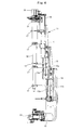
- FIG. 1A is a side configuration diagram schematically showing the overall structure of the transmission type small angle scattering device according to the embodiment of the present invention.
- FIG. 1B is also a front configuration view.
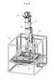
- FIG. 2 is a perspective view showing the appearance of the transmission type small angle scattering device according to the embodiment of the present invention.
- FIG. 3 is a perspective view of the appearance of the transmission type small-angle scattering device according to the embodiment of the present invention as viewed from a direction different from that of FIG.
- FIG. 4 is a perspective view showing the appearance of the swivel arm of the goniometer constituting the transmission type small-angle scattering device according to the embodiment of the present invention and the components mounted on the swivel arm.
- FIG. 1A is a side configuration diagram schematically showing the overall structure of the transmission type small angle scattering device according to the embodiment of the present invention.
- FIG. 1B is also a front configuration view.
- FIG. 2 is a perspective view showing the appearance of the transmission type small angle scattering device
- FIG. 5 is a perspective view showing a state in which the swivel arm of the goniometer shown in FIG. 4 is folded to shorten the total length.
- FIG. 6 is a diagram schematically showing an optical system configured between an X-ray irradiation unit and a two-dimensional X-ray detector.
- FIG. 7 is a perspective view showing the appearance of the sample stage constituting the transmission type small angle scattering device according to the embodiment of the present invention.
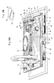
- FIG. 8 is an enlarged plan view showing a sample holding portion for supporting the sample and an in-plane rotation mechanism.
- FIG. 9 is an enlarged perspective view showing a sample holding portion for supporting the sample and an in-plane rotation mechanism.
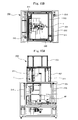
- FIG. 10A is a perspective view showing an X-axis moving mechanism, a Y-axis moving mechanism, and a Z-axis moving mechanism.
- FIG. 10B is a configuration diagram schematically showing a guide member and a sliding member.
- FIG. 11 is a perspective view showing the ⁇ -axis swing mechanism.
- FIG. 12 is a vertical cross-sectional view of the sample stage.
- FIG. 13 is a perspective view showing a state in which the transmission type small angle scattering device according to the embodiment of the present invention is covered with an outer housing.
- FIG. 14 is a perspective view showing a state in which the outer housing according to the embodiment of the present invention is folded.
- FIG. 15A is a left side view showing a state in which the transmission type small angle scattering device according to the embodiment of the present invention is covered with an outer housing.
- FIG. 15B is also a plan view.
- FIG. 16 is a vertical cross-sectional view showing a state in which the transmission type small angle scattering device according to the embodiment of the present invention is covered with an outer housing.
- FIG. 17 is a perspective view showing the appearance of a semiconductor inspection device incorporating the transmission type small-angle scattering device according to the embodiment of the present invention.
- FIG. 18 is a block diagram showing a control system of the transmission type small angle scattering device according to the embodiment of the present invention.
- FIG. 20A is a frontal configuration diagram schematically showing a configuration example relating to a means for measuring the inclination of the semiconductor wafer.
- FIG. 20B is a side configuration diagram schematically showing another configuration example relating to a means for measuring the inclination of the semiconductor wafer.
- the small-angle scattering device is a reflective small-angle scattering device that irradiates the surface of the sample with X-rays and detects the scattered X-rays reflected from the surface of the sample, and the back surface of the sample is irradiated with X-rays and emitted from the surface.
- the present invention is a transmission type small angle scattering device.
- this transmission type small angle scattering device an X-ray source and a two-dimensional X-ray detector are arranged so as to face each other across the sample, X-rays from the X-ray source are irradiated to the back surface of the sample, and a specific angle from the surface of the sample. It has a basic structure that detects scattered X-rays emitted from the X-ray detector with a two-dimensional X-ray detector.
- FIG. 1A is a side configuration diagram schematically showing the overall structure of the transmission type small angle scattering device according to the embodiment of the present invention
- FIG. 1B is also a front configuration diagram. 2 and 3 are perspective views of the appearance of the transmission type small-angle scattering device as viewed from different directions.
- the transmission type small-angle scattering device includes a goniometer 10.
- the goniometer 10 has a function of swinging and driving the swivel arm 11 around a ⁇ -axis extending in the horizontal direction.
- the swivel arm 11 is equipped with an X-ray irradiation unit 20 and a two-dimensional X-ray detector 30 at both ends thereof.
- the swivel arm 11 has its origin in the vertically arranged state.
- the X-ray irradiation unit 20 is mounted on the lower end portion, and the two-dimensional X-ray detector 30 is mounted on the upper end portion. With such a vertical arrangement structure, it can be installed even on a floor surface having a relatively small area.
- the X-ray irradiation unit 20 and the two-dimensional X-ray detector 30 are arranged so as to face each other with the sample stage 40 in between, and the X-ray irradiation unit with respect to the sample S supported by the sample holding portion 42 of the sample stage 40. 20 irradiates X-rays from below. Then, the two-dimensional X-ray detector 30 detects the scattered X-rays generated in the minute angle region around the X-rays transmitted from the sample S.
- the sample stage 40 is formed with a cavity 43 that transmits X-rays emitted from the X-ray irradiation unit 20, and is formed on the back surface of the sample S through the cavity 43. It is configured to irradiate X-rays.
- a cylindrical vacuum path 32 is mounted on the swivel arm 11 of the goniometer 10.
- the vacuum path 32 has a function of eliminating air scattering generated when X-rays transmitted through the sample S collide with air and improving the measurement accuracy of small-angle scattering.
- the sample stage 40 is driven by a sample positioning mechanism described later to move the sample holding portion 42 in the front-rear direction (Y direction) and the lateral direction (X direction) parallel to the horizontal plane and the vertical direction (Z direction) perpendicular to the horizontal plane, respectively. It has a configuration in which the point to be inspected of the sample S is moved and positioned at the measurement position P of the transmission type small angle scattering device.
- the sample positioning mechanism has a function of in-plane rotation ( ⁇ rotation) of the sample S supported by the sample holding portion 42. Further, the sample positioning mechanism has a function of swinging the sample S supported by the sample holding portion 42 around the ⁇ axis ( ⁇ swing). This ⁇ axis intersects the ⁇ axis of the goniometer 10 at right angles in the horizontal plane. The intersection of the ⁇ -axis and the ⁇ -axis is positioned so as to match the measurement position P of the transmission type small-angle scattering device.
- the sample stage 40 is supported by the frame 41 as shown in FIGS. 2 and 3.
- the frame body 41 and the swivel arm 11 of the goniometer 10 are adjusted in mutual positional relationship so as not to interfere with each other.
- the transmission type small angle scattering device includes an optical microscope 35 that recognizes the surface of the sample S.
- the optical microscope 35 is installed at a position that does not interfere with the surrounding components such as the parts driven by the sample positioning mechanism, the X-ray irradiation unit 20 swirled by the goniometer 10, and the two-dimensional X-ray detector 30. ..
- the sample S can be moved to a lower position of the optical microscope 35 by the sample positioning mechanism.
- FIG. 4 is a perspective view showing the appearance of the swivel arm of the goniometer constituting the transmission type small-angle scattering device according to the present embodiment and the components mounted on the swivel arm.
- FIG. 5 is a perspective view showing a state in which the swivel arm of the goniometer shown in FIG. 4 is folded to shorten the total length.
- the swivel arm 11 of the goniometer 10 is composed of a plurality of arm members.
- the swivel arm 11 of the present embodiment shown in FIGS. 4 and 5 is composed of first, second, and third arm members 12, 13, and 14, and the first arm member 12 is a goniometer ⁇ rotation axis (FIG. 1A). It is fixed to the ⁇ axis).
- the second arm member 13 slides in the longitudinal direction with respect to the first arm member 12, and the third arm member 14 slides in the longitudinal direction with respect to the second arm member 13, as shown in FIG. ,
- Each arm member 12, 13 and 14 are overlapped and folded. By folding each arm member 12, 13 and 14 in this way, the total length can be shortened and a compact form can be obtained.
- the transport work and the installation work at the site become extremely easy, and the work time required for the work and the labor can be reduced.
- a guide rail 12a is provided on the surface of the first arm member 12 in the longitudinal direction, and the second arm member 13 is slidable along the guide rail 12a.
- a guide rail 13a is provided on the surface of the second arm member 13 in the longitudinal direction, and the third arm member 14 is slidable along the guide rail 13a.
- each arm member 12, 13, 14 is unfolded to extend the total length, and as shown in FIG. 5, each arm member 12, 13, 14 is folded.
- a lock mechanism (not shown) is incorporated to hold the state in which the total length is shortened.
- a lower holding member 15 for mounting the X-ray irradiation unit 20 is provided at the lower end of the first arm member 12.
- the X-ray irradiation unit 20 is fixed to the lower holding member 15.
- the lower holding member 15 incorporates a slide mechanism (not shown) for moving and adjusting the fixed position of the X-ray irradiation unit 20 in the longitudinal direction.
- an upper holding member 16 for mounting the two-dimensional X-ray detector 30 is provided at the upper end portion of the third arm member 14.
- the two-dimensional X-ray detector 30 is fixed to the upper holding member 16.
- the upper holding member 16 also incorporates a slide mechanism (not shown) for moving and adjusting the fixed position of the two-dimensional X-ray detector 30 in the longitudinal direction.
- a direct beam stopper 31 is installed in front of the two-dimensional X-ray detector 30.
- the direct beam stopper 31 has a function of shielding the X-rays that have passed through the sample S from the X-ray irradiation unit 20 and traveling straight, and preventing the X-rays from entering the two-dimensional X-ray detector 30.
- the swivel arm 11 is also equipped with a vacuum path 32 as described above.
- Each arm member 12, 13 and 14 is provided with a support member 17 for supporting the vacuum path 32.
- the vacuum path 32 is supported by these support members 17 and is arranged on the optical path of the X-rays that have passed through the sample S and the scattered X-rays generated around the X-rays.
- the upper end surface of the vacuum path 32 is positioned in the vicinity of the two-dimensional X-ray detector 30.
- the vacuum path 32 has a structure in which the diameter of the lower end surface facing the sample S is reduced and the diameter is gradually increased toward the upper end surface.
- the inside of the vacuum path 32 is sealed to form a vacuum state, and both end faces are formed of a material such as carbon, boron carbide, or Kapton, which has a small X-ray absorption rate.
- FIG. 6 is a diagram schematically showing an optical system configured between an X-ray irradiation unit and a two-dimensional X-ray detector.
- the X-ray irradiation unit 20 includes an X-ray tube 21, a condensing mirror 22, and an aperture 23 as components. Further, a guard slit 24 is arranged in front of the sample S.
- an X-ray tube having an electron beam focal size of 70 ⁇ m or less, preferably 40 ⁇ m or less on the target is used.
- Copper (Cu), molybdenum (Mo), silver (Ag), gold (Au), etc. can be selected as the target material, but in the case of the transmission type, high-energy X-rays capable of transmitting through the Si wafer as the substrate are required. Therefore, it is desirable to use molybdenum (Mo) or silver (Ag) that makes it possible.
- a side-by-side condensing mirror 22 in which two multilayer mirrors having a multilayer film formed on the surface thereof are arranged in an L shape and integrated can be adopted.
- a Kirkpatrick Baez type condensing mirror in which two multilayer mirrors are independently arranged may be adopted.
- the condensing mirror 22 is adjusted so as to focus on the detection surface of the two-dimensional X-ray detector 30, and has a function of condensing X-rays on a rectangular spot having a focal point of 100 ⁇ m or less, preferably 50 ⁇ m or less. There is.
- the aperture 23 has a function of shielding the leaked light that the X-rays emitted from the X-ray tube 21 do not enter the condensing mirror 22 and pass through the outside as it is.
- the X-rays emitted from the X-ray tube 21 are shielded from leaked light by the aperture 23, and subsequently monochromatic and converged by the condensing mirror 22.
- the guard slit 24 is a single crystal pinhole slit made of a single crystal of germanium, and is supported by a slit support member (not shown) provided on the swivel arm 11 and arranged in front of the sample S.
- a normal slit has a drawback that when it is exposed to X-rays, parasitic scattering occurs and the background becomes large.
- the guard slit 24 made of a single crystal of germanium can reduce parasitic scattering and suppress the background.
- a slit 25 for further reducing the cross-sectional area of X-rays may be arranged between the condensing mirror 22 and the guard slit 24.
- the X-rays emitted from the X-ray tube 21 are shielded by the aperture 23 and enter the condensing mirror 22. Then, the X-rays monochromatic and focused by the condensing mirror 22 are narrowed in cross section by the guard slit 24 and irradiated to the inspection point having a small area on the sample S.
- the X-rays transmitted through the sample S and the scattered X-rays generated in the small angle region around the sample S travel toward the two-dimensional X-ray detector 30 through the vacuum path 32 shown in FIG.
- the X-rays that have passed through the sample S from the X-ray irradiation unit 20 and traveled straight are shielded by the direct beam stopper 31 provided in front of the two-dimensional X-ray detector 30.
- the direct beam stopper 31 provided in front of the two-dimensional X-ray detector 30.
- the distance L1 from the focal point of the X-ray tube 21 to the sample S affects the focused area of the X-rays applied to the sample S. That is, the longer the distance L1, the smaller the focused area of the X-rays irradiated on the sample S.
- the distance L2 from the sample S to the two-dimensional X-ray detector 30 is referred to as a camera length, and this camera length L2 affects the angular resolution of the two-dimensional X-ray detector 30. That is, the longer the camera length L2, the better the angular resolution.
- the camera length L2 can be arbitrarily set by appropriately adjusting the slide positions of the sliding arm members 13 and 14.
- the swivel arm 11 can also be provided with a position adjusting mechanism for moving the X-ray irradiation unit 20 in the optical axis direction of the X-rays and arbitrarily changing the distance L1. Further, a position adjusting mechanism for moving the two-dimensional X-ray detector 30 in the optical axis direction of X-rays and arbitrarily changing the camera length L2 may be mounted on the swivel arm 11.
- FIG. 7 is a perspective view showing the appearance of the sample stage constituting the transmission type small angle scattering device according to the present embodiment.
- FIG. 8 is an enlarged plan view of the sample holding portion that supports the sample, and
- FIGS. 9 to 11 are perspective views and views in which different parts of the sample stage are focused on in order to explain the sample positioning mechanism.
- 12 is a vertical sectional view of the sample stage.
- the sample stage 40 includes a sample holding unit 42 that supports the sample S and a sample positioning mechanism that drives the sample holding unit 42.
- the sample positioning mechanism includes an in-plane rotation mechanism for in-plane rotation ( ⁇ -rotation) of the sample S supported by the sample holding portion 42 and a front-back direction parallel to the surface of the sample S supported by the sample holding portion 42.
- the Y-axis moving mechanism for moving the sample holding portion 42 in the Y-axis direction) and the sample holding portion 42 in the lateral direction (X-axis direction) parallel to the surface of the sample S supported by the sample holding portion 42.
- An X-axis moving mechanism for moving includes a Z-axis moving mechanism for moving the sample holding portion 42 in the vertical direction (Z-axis direction) perpendicular to the surface of the sample S supported by the sample holding portion 42, and a sample. It includes a ⁇ -axis swing mechanism that swings the holding portion 42 around the ⁇ -axis.
- the X-axis moving frame 51 is mounted on the base frame 50
- the ⁇ -axis swivel table 52 is mounted on the X-axis moving frame 51
- ⁇ The Y-axis moving table 53 is mounted on the shaft swivel table 52
- the Z-axis drive table 54 and the Z-axis moving table 55 are mounted on the Y-axis moving table 53
- the sample is mounted on the Z-axis moving table 55.
- the sample holding frame 56 forming the holding portion 42 is mounted.
- the sample holding portion 42 is formed inside the circular sample holding frame 56.
- the inside of the sample holding frame 56 is an X-ray transmission hole 57, and the sample S is supported in a state of facing the X-ray transmission hole 57.
- suction support pieces 58 are provided so as to project inward from a plurality of locations (4 locations in the figure).
- a part of the outer peripheral edge of the sample S is arranged on the upper surface of the suction support pieces 58, and the sample S is vacuum sucked on the upper surface of the suction support pieces 58.
- a vacuum nozzle 59 is opened on the upper surface of each suction support piece 58, and the vacuum nozzle 59 is vacuum sucked by a vacuum suction device (not shown).
- the X-ray transmission hole 57 formed inside the sample holding frame 56 communicates with the cavity 43 of the sample stage 40 shown in FIGS. 1A and 1B (see FIG. 12).
- the X-rays emitted from the X-ray irradiation unit 20 pass through the X-ray transmission hole 57 from the cavity 43 and irradiate the back surface of the sample S supported by the adsorption support piece 58.
- the conventional X-ray inspection apparatus has a configuration in which the sample holding portion 42 is formed of a material having a low X-ray absorption rate such as Kapton, and the entire back surface of the sample S is arranged in close contact with the upper surface of the sample holding portion 42. It is common. However, for example, when a semiconductor device formed on a semiconductor wafer is an inspection target, the back surface of the semiconductor wafer may come into contact with the sample holding portion 42 formed of a material such as Kapton and be contaminated.
- the back surface of the sample S is a semiconductor wafer on which a circuit pattern is formed because only a limited part of the outer peripheral edge portion comes into contact with the suction support piece 58.
- the sample S can be supported without touching the central portion.
- X-rays from the X-ray irradiation unit 20 can be irradiated through the cavity 43 and the X-ray transmission hole 57 to almost the entire area of the sample S excluding a part of the minute region supported by the adsorption support piece 58, measurement is possible. A wide area can be secured. It is possible to irradiate a part of the minute region supported by the suction support piece 58 with X-rays by changing the suction position by the sample S transfer robot.
- the sample holding frame 56 constituting the sample holding portion 42 has a rotation guide portion 60 formed on a circular outer peripheral edge portion, and the rotation guide portions 60 are provided at a plurality of locations (4 locations in the figure) on the upper surface of the Z-axis moving table 55. ),
- the rotation support portion 61 is rotatably supported in the plane. Each rotation support portion 61 supports the rotation guide portion 60 from the vertical direction by a pair of upper and lower support rollers 62.
- a driven side pulley 63 is formed on the sample holding frame 56. Further, an in-plane rotation drive motor 64 is installed on the Z-axis moving table 55, and the drive side pulley 65 provided on the drive shaft of the in-plane rotation drive motor 64 and the driven side of the sample holding frame 56 are provided. A drive belt 66 is wound between the pulley 63 and the drive belt 66.
- the in-plane rotation mechanism is composed of the components of the rotation guide portion 60, the rotation support portion 61, the in-plane rotation drive motor 64, the drive side pulley 65, the driven side pulley 63, and the drive belt 66. That is, the rotational driving force from the in-plane rotational drive motor 64 is transmitted to the sample holding frame 56 via the drive belt 66. The rotation driving force causes the sample holding frame 56 supported by the rotation support portion 61 to rotate in-plane.
- the X-axis moving frame 51 is mounted on the base frame 50 via an X-axis moving mechanism.
- the X-axis moving mechanism includes an X-axis driving motor 67, a ball screw 68, a guide rail 71, and a slider 72.
- the X-axis drive motor 67, the screw shaft 69 of the ball screw 68, and the guide rail 71 are installed on the base frame 50.
- the guide rail 71 extends in the X-axis direction, and the slider 72 is movable along the guide rail 71.
- the guide rails 71 are installed at both ends of the base frame 50, and the sliders 72 combined with the guide rails 71 movably support the X-axis moving frame 51.
- the screw shaft 69 of the ball screw 68 is rotatably supported by a bearing 73 provided on the base frame 50 and extends in the X-axis direction.
- the screw shaft 69 is connected to the rotary drive shaft of the X-axis drive motor 67, and is rotationally driven by the rotary drive force of the motor 67.
- a nut member 70 is meshed with the screw shaft 69, and the nut member 70 moves in the X-axis direction as the screw shaft 69 rotates.
- the nut member 70 is fixed to the X-axis moving frame 51, and the X-axis moving frame 51 moves integrally with the nut member 70 in the X-axis direction.
- the X-axis moving frame 51 is provided with a pair of bearings 52a at both ends, via a swing support shaft 74 swingably supported by these bearings 52a. Therefore, the ⁇ -axis swivel base 52 is mounted swingably. Then, the Y-axis moving table 53 is mounted on the ⁇ -axis swivel table 52 via the Y-axis moving mechanism.
- the Y-axis moving mechanism includes a Y-axis drive motor 75, a ball screw 76, and a guide rail 91 and a slider 92 shown in FIG.
- the guide rails 91 are provided at both ends of the ⁇ -axis swivel table 52 and extend in the Y-axis direction.
- Sliders 92 are movably combined with each guide rail 91, and the Y-axis moving base 53 is supported by these sliders 92.
- a Y-axis drive motor 75 and a screw shaft 77 of the ball screw 76 are installed on the side wall of the ⁇ -axis swivel base 52.
- the screw shaft 77 of the ball screw 76 is rotatably supported by a bearing 78 provided on the side wall of the ⁇ -axis swivel base 52 and extends in the Y-axis direction.
- the screw shaft 77 is connected to the rotary drive shaft of the Y-axis drive motor 75, and is rotationally driven by the rotary drive force of the motor 75.
- a nut member 79 is meshed with the screw shaft 77, and the nut member 79 moves in the Y-axis direction as the screw shaft 77 rotates.
- the nut member 79 is fixed to the Y-axis moving table 53, and the Y-axis moving table 53 moves integrally with the nut member 79 in the Y-axis direction.
- a Z-axis drive base 54 is mounted on the Y-axis moving base 53.
- a guide rail 93 extending in the Y-axis direction is installed on the Y-axis moving table 53, and a slider 94 is combined with the guide rail 93 (see FIG. 12).
- the Z-axis drive base 54 is supported by the slider 94 and mounted on the Y-axis moving base 53.
- a ball screw 95 shown in FIG. 12 and a Z-axis drive motor 80 shown in FIG. 10A are installed on the Y-axis moving table 53, and the screw of the ball screw 95 is attached to the rotary drive shaft of the motor 80.
- the axes are connected.
- the screw shaft is rotatably supported on the Y-axis moving table 53 by a bearing (not shown).
- the nut member 96 shown in FIG. 12 is meshed with the screw shaft, and the nut member 96 moves in the Y-axis direction as the screw shaft rotates.
- the nut member 96 is fixed to the Z-axis drive base 54, and the Z-axis drive base 54 moves integrally with the nut member 96 in the Y-axis direction.
- the Z-axis moving table 55 is supported on the Z-axis drive table 54 via a guide member 81 and a sliding member 82 that are combined in a rust shape as shown in FIG. 10B.
- the guide members 81 are installed at both ends of the Z-axis drive base 54, respectively.
- the sliding member 82 combined with each of the guide members 81 is fixed to the bottom surface of the Z-axis moving table 55.
- guide rails 83 extending in the Z-axis direction are installed at both ends of the Y-axis moving table 53, and a slider 84 combined with the guide rail 83 is fixed to the Z-axis moving table 55.
- the Z-axis moving table 55 is movable in the Z-axis direction integrally with the slider 84 along the guide rail 83.
- the guide member 81 also moves integrally in the same direction.
- the wedge-shaped combined sliding member 82 is pushed up in the Z-axis direction.
- the guide member 81 also moves integrally in the same direction, and the wedge-shaped sliding member 82 descends.
- the Z-axis moving table 55 moves in the vertical direction along the guide rail 83. Since the guide member 81 and the sliding member 82, which are combined in a wedge shape, are always in a sliding contact state without rattling, the sample holding portion 42 is accurately moved in the vertical direction to a desired height position. Can be positioned.
- the ⁇ -axis swing mechanism is incorporated between the X-axis moving frame 51 and the ⁇ -axis swivel base 52. That is, the ⁇ -axis swing mechanism includes a ⁇ -axis drive motor 85, a driving force transmission belt 86, a worm 87, and a worm wheel 88.
- the fan-shaped worm wheel 88 is provided at a position below the bearing 52a provided at one end of the X-axis moving frame 51, and its pitch circle is positioned on the same axis of the swing support shaft 74 supported by the bearing 52a. ing.
- the ⁇ -axis drive motor 85 and the worm 87 are installed on the outer surface of the side wall of the ⁇ -axis swivel base 52.
- a driving force transmission belt 86 is wound between the drive-side pulley 89 provided on the rotary drive shaft of the ⁇ -axis drive motor 85 and the driven-side pulley 90 provided on the rotary shaft of the worm 87.
- the rotational driving force from the ⁇ -axis driving motor 85 is transmitted to the worm 87 via the driving force transmission belt 86.
- the worm 87 rotates and rotates along the pitch circle of the worm wheel 88, and the ⁇ -axis swivel base 52 rotates around the swing support shaft 74 integrally with the worm 87.
- the central axis of the swing support shaft 74 is positioned so as to coincide with the ⁇ axis shown in FIG. 1B.
- the optical axis angle of the incident X-ray with respect to the sample S supported by the sample holding portion 42 can be arbitrarily changed by driving the above-mentioned ⁇ -axis swing mechanism and the swivel arm 11 of the goniometer 10.
- the sample stage 40 of the present embodiment has a lower end opening that captures incident X-rays from an upper end opening 43a that communicates the cross section of the cavity 43 with the X-ray transmission hole 57 of the sample holding frame 56.
- the configuration is widened toward 43b.
- the angle range in which the incident X-rays can be tilted without being blocked by the members around the cavity 43 is widened, and is flexible to various measurement conditions. It becomes possible to correspond to.
- the semiconductor wafer (sample S) having a radius of 150 mm has a structure that can be inclined up to an angle of 20 ° with respect to the optical axis of X-rays incident from the vertical direction. ..
- FIG. 13 is a perspective view showing a state in which the transmission type small angle scattering device according to the present embodiment is covered with an outer housing.
- 15A is a left side view
- FIG. 15B is a plan view
- FIG. 16 is a vertical sectional view.
- FIG. 14 is a perspective view showing a state in which the outer housing is folded.
- a transmission type small-angle scattering device that uses X-rays is installed in a state of being covered with an external housing for protection against X-rays.
- the transmission type small-angle scattering device 1 has a vertically long structure in order to irradiate the sample S supported by the sample holding portion 42 with X-rays in the vertical direction (FIG. 1A-3). Therefore, as shown in FIG. 13, the outer housing 200 also has a vertically long structure.
- the external housing 200 is composed of a housing body 201 and a plurality of housing element members 202, 203, and each housing element member 202, 203 is attached to the housing body 201. It has a structure that can be moved in the vertical direction. Specifically, as shown in FIGS. 15A and 15B, the housing element member 202 in the middle stage with respect to the housing body 201 is movable in the vertical direction along the guide rail 210, and further, the housing is movable. The upper housing element member 203 with respect to the element member 202 is movable in the vertical direction along the guide rail 211. Then, the driving force from the drive motor (not shown) is transmitted to the housing element members 202 and 203 via a drive mechanism (not shown) to drive the housing element members 202 and 203 in the vertical direction. ..
- the housing element members 202 and 203 are both moved to the lower position and folded on the inside of the housing body 201. It is in the state. As described above, by adopting a compact form having a small height dimension, the transportation work and the installation work of the outer housing 200 become extremely easy, and the work time required for the work can be shortened and the labor can be reduced. .. Since the outer housing 200 is a heavy object, disassembling and assembling the housing element members 202 and 203 with respect to the housing body 201 complicates the disassembling and assembling work. By adopting a structure that drives the housing element members 202 and 203 in the vertical direction, the on-site disassembly / assembly work becomes unnecessary, and the on-site installation work and removal work become easier.
- FIGS. 13 to 15A in order to visually recognize the inside of the outer housing 200, a part or all of the wall surface covering the transmission type small-angle scattering device is omitted. Further, a substrate transfer device 310 is provided in front of the outer housing 200 as described later, but a wall surface is not provided at the side of the board transport device 310, and the board is configured to communicate with the inside of the outer housing 200. ..
- the internal space of the outer housing 200 is vertically partitioned by a shielding panel 220 horizontally arranged above the sample stage 40. Then, in the lower space partitioned by the shielding panel 220 (that is, the lower space in which the sample stage 40 is installed), dust is removed with high accuracy from the fan filter unit 300 provided outside the outer housing 200. Air is supplied. As a result, the lower space becomes a clean space with extremely little dust, and it is possible to prevent dust from adhering to the semiconductor wafer (sample S) supported by the sample holding portion 42.
- the shielding panel 220 shields the upward flow of air from the fan filter unit 300, and realizes an efficient and economical supply of air to the semiconductor wafer and its surroundings.
- FIG. 17 is a perspective view showing the appearance of a semiconductor inspection device incorporating the transmission type small-angle scattering device according to the present embodiment.
- a substrate transfer device (EFEM) 310 and an electrical component 320 are provided outside the outer housing 200 that covers the periphery of the transmission type small-angle scattering device.
- Semiconductor inspection equipment is constructed.
- the substrate transfer device 310 has a function of automatically transferring the semiconductor wafer (sample S) to be measured to the sample holding unit 42 and automatically carrying out the semiconductor wafer for which measurement has been completed from the sample holding unit 42.
- the semiconductor wafer is automatically transported in a state of being stored in a closed cassette (FOUP).
- the electrical component 320 is provided with a power source for supplying electric power to the transmission type small-angle scattering device and a computer for controlling the device.
- the semiconductor inspection apparatus is provided with equipment for supplying utilities (not shown). With these configurations, the semiconductor inspection device incorporating the transmission type small-angle scattering device according to the present embodiment automatically conveys the semiconductor wafer and realizes in-line automatic measurement in the middle of the semiconductor manufacturing process.
- FIG. 18 is a block diagram showing a control system of the transmission type small angle scattering device according to the present embodiment.
- the control of the X-ray irradiation unit 20 is executed by the X-ray irradiation controller 101.
- the image of the sample S captured by the optical microscope 35 is image-recognized by the image recognition circuit 102.
- the optical microscope 35 and the image recognition circuit 102 constitute an image observing means for observing an image of the sample S arranged in the sample holding unit 42.
- the focal position of the optical microscope 35 is adjusted by the focus controller 103.
- the positioning controller 104 drives and controls the sample positioning mechanism 110.
- the positioning controller 104 positions the sample based on the image of the sample S captured by the optical microscope 35 and recognized by the image recognition circuit 102.
- the mechanism 110 is driven and controlled.
- the goniometer 10 is driven and controlled by the goniometer controller 105.
- Each component of the X-ray irradiation controller 101, the image recognition circuit 102, the focus controller 103, the positioning controller 104, and the gonio controller 105 operates based on the setting information sent from the central processing unit 100.
- the setting information is stored in the storage unit 106 in advance as a recipe, and the central processing unit 100 reads it out and outputs it to each of the above-mentioned components.
- the two-dimensional X-ray detector 30 is controlled by the detection control circuit 107.
- FIG. 19 is a flowchart showing an execution procedure of a measurement operation by the transmission type small-angle scattering device according to the present embodiment having the above-described configuration.
- the measurement operation when the semiconductor wafer on which the circuit pattern of the semiconductor device is formed is used as the sample S will be described.
- Software for executing small-angle scattering measurement is stored in advance in the storage unit 106, and the central processing unit 100 (CPU) executes the following processing steps according to the software.
- the positioning controller 104 After sucking and supporting the semiconductor wafer, which is the sample S to be inspected, on the sample holding unit 42, the positioning controller 104 first drives and controls the sample positioning mechanism 110 to arrange the semiconductor wafer at a position below the optical microscope 35 (step). S1).
- the image recognition circuit 102 recognizes the unique point formed on the surface of the semiconductor wafer based on the image data from the optical microscope 35 (step S2).
- unique points formed on the surface of the semiconductor wafer are stored in advance as recipes.
- a portion that can be recognized by the image recognition circuit 102 without hesitation is set based on the image information from the optical microscope 35, such as a characteristic pattern shape formed on the surface of the semiconductor wafer.
- the positioning controller 104 drives and controls the sample positioning mechanism 110 based on the position information of the inspected point set in advance, and sets the inspected point as an apparatus. It is arranged at the measurement position P of (step S3).
- step S4 small-angle scattering measurement is executed (step S4), and the central processing unit 100 analyzes the measurement data (step S5).
- shape analysis measurement such as analysis of the tilt angle of a deep hole formed on the surface of a semiconductor wafer
- the swing arm 11 of the goniometer 10 is driven, or the semiconductor is driven by a ⁇ -axis swing mechanism.
- shape analysis such as analysis of the tilt angle of a deep hole formed on the surface of a semiconductor wafer
- the swing arm 11 of the goniometer 10 is driven, or the semiconductor is driven by a ⁇ -axis swing mechanism.
- step S6 Each step of S3 to S5 described above is executed for all the inspection points set on the semiconductor wafer (step S6), small-angle scattering measurement is executed for all the inspection points, and then the measurement operation is terminated.
- the semiconductor device is usually formed on a semiconductor wafer, and scatterers to be measured are periodically arranged in a direction parallel to the main surface of the semiconductor wafer.
- Examples of the measurement target include minute holes and pillars constituting the semiconductor device.
- miniaturization and high integration are evolving day by day, and there are cases where the diameter of holes and pillars is several tens of nm and the depth (height) is several ⁇ m, resulting in extremely fine and high aspect ratio.
- the transmission type small-angle scattering device according to the present embodiment for such a structure, it is possible to specify the accurate three-dimensional shape of these holes and pillars.
- FIG. 20A is a frontal configuration diagram schematically showing a configuration example relating to a means for measuring the inclination of the semiconductor wafer.
- a laser tilt measuring device 36 is attached to the swivel arm 11 of the goniometer 10 together with a two-dimensional X-ray detector 30.
- the two-dimensional X-ray detector 30 and the laser tilt measuring device 36 are mounted on a moving table 37 that moves in the lateral direction. Then, the moving table 37 moves laterally with the driving force of a drive motor (not shown), and the two-dimensional X-ray detector 30 is placed at a position facing the optical axis O of the X-rays emitted from the X-ray irradiation unit 20.
- the structure is such that either one of the laser tilt measuring instruments 36 can be switched and arranged.
- the laser tilt measuring device 36 includes a laser light source 36a and a laser detector 36b, and irradiates the surface of the semiconductor wafer (sample S) supported by the sample holding portion 42 with the laser light from the laser light source 36a to form the same surface. By detecting the laser beam reflected from the laser detector 36b with the laser detector 36b, it has a function of measuring the inclination of the surface of the semiconductor wafer with respect to the optical axis O.
- the ⁇ -axis swing mechanism and the in-plane rotation mechanism of the sample stage 40 are driven with respect to the optical axis O of the incident X-ray. Adjust so that the surface of the semiconductor wafer is vertical.
- the optical axis angle of X-rays with respect to the semiconductor wafer can be arbitrarily changed.
- FIG. 20B is a side configuration diagram schematically showing another configuration example relating to a means for measuring the inclination of the semiconductor wafer.
- the laser inclination measuring device 36 is installed side by side with the optical microscope 35.
- the semiconductor wafer (sample S) supported by the sample holding portion 42 by driving the Y-axis moving mechanism and the X-axis moving mechanism of the sample stage 40 is mounted on the laser inclination measuring device 36. Move it to the lower position.
- the laser tilt measuring device 36 measures the tilt of the surface of the semiconductor wafer by irradiating the surface of the semiconductor wafer with the laser light from the laser light source 36a and detecting the laser light reflected from the surface by the laser detector 36b. It has a function that can be used. Here, for example, if the positions of the laser light source 36a and the laser detector 36b are adjusted in advance so that the laser inclination measuring device 36 can measure the inclination with reference to the horizontal plane, the surface of the semiconductor wafer with respect to the horizontal plane or the vertical axis can be adjusted. The tilt can be measured.
- the swivel arm is not limited to the configuration of the three arm members 12, 13 and 14 as shown in FIG. 4, and may be composed of two or four or more arm members.
- the external housing is not limited to a configuration in which the two housing element members 202 and 203 are movable with respect to the housing main body 201, and the housing is not limited to the housing.
- One or three or more housing element members may be movable with respect to the main body. Further, the movement of these housing element members can be configured to be manually moved as needed, in addition to the driving force from the driving motor.
Landscapes
- Chemical & Material Sciences (AREA)
- Crystallography & Structural Chemistry (AREA)
- Physics & Mathematics (AREA)
- Health & Medical Sciences (AREA)
- Life Sciences & Earth Sciences (AREA)
- Analytical Chemistry (AREA)
- Biochemistry (AREA)
- General Health & Medical Sciences (AREA)
- General Physics & Mathematics (AREA)
- Immunology (AREA)
- Pathology (AREA)
- Analysing Materials By The Use Of Radiation (AREA)
- Testing Or Measuring Of Semiconductors Or The Like (AREA)
- Length-Measuring Devices Using Wave Or Particle Radiation (AREA)
Abstract
Description
このような縦型の配置構造とすることで、比較的狭い面積の床面にも設置することができる。
このように各アーム部材を畳むことにより、全長を短くしてコンパクトな形態とすることができる。
さらに、試料保持枠の内周縁には、複数箇所から吸着支持片を内側へ突き出して設け、これら吸着支持片によって試料の外周縁部の一部分を吸着支持する構成としてもよい。
しかも、吸着支持片によって支持された一部の微小領域を除く試料のほぼ全域に対し、X線照射ユニットからのX線をX線透過孔を通して照射できるため、測定可能領域を広く確保することができる。
この構成によれば、くさび状に組み合わされた案内部材と摺動部材との間は常にがたつくことなく摺接状態を保っているので、試料保持部を正確に上下方向へ移動させて所望の高さ位置へ位置決めすることができる。
筐体要素部材を筐体本体に重ねて畳んだ状態とすることで、高さ寸法の小さいコンパクトな形態を形成でき、外部筐体の運搬作業や設置作業がきわめて容易となる。
10:ゴニオメータ、11:旋回アーム、12:第1アーム部材、13:第2アーム部材、14:第3アーム部材、12a,13a:案内レール、15:下部保持部材、16:上部保持部材、17:支持部材
20:X線照射ユニット、21:X線管、22:集光ミラー、23:アパーチャ、24:ガードスリット、25:スリット
30:二次元X線検出器、31:ダイレクトビームストッパ、32:真空パス、
35:光学顕微鏡、36:レーザ傾き測定器、36a:レーザ光源、36b:レーザ検出器、37:移動テーブル、
40:試料ステージ、41:枠体、42:試料保持部、43:空洞、50:基枠、51:X軸移動枠、52:χ軸旋回台、52a:軸受、53:Y軸移動台、54:Z軸駆動台、55:Z軸移動台、56:試料保持枠、57:X線透過孔、58:吸着支持片、59:真空ノズル、60:回転ガイド部、61:回転支持部、62:支持ローラ、63:従動側プーリ、64:面内回転用駆動モータ、65:駆動側プーリ、66:駆動ベルト、67:X軸駆動用モータ、68:ボールねじ、69:ねじ軸、70:ナット部材、71:案内レール、72:スライダ、73:軸受、74:揺動支軸、75:Y軸駆動用モータ、76:ボールねじ、77:ねじ軸、78:軸受、79:ナット部材、80:Z軸駆動用モータ、81:案内部材、82:摺動部材、83:案内レール、84:スライダ、85:χ軸駆動用モータ、86:駆動力伝達ベルト、87:ウォーム、88:ウォームホイール、89:駆動側プーリ、90:従動側プーリ、91:案内レール、92:スライダ、93:案内レール、94:スライダ、95:ボールねじ、96:ナット部材、
100:中央処理装置、101:X線照射コントローラ、102:画像認識回路、103:フォーカスコントローラ、104:位置決めコントローラ、105:ゴニオコントローラ、106:記憶部、107:検出制御回路、110:試料位置決め機構、
200:外部筐体、201:筐体本体、202,203:筐体要素部材、210,211:案内レール、220:遮蔽パネル、
300:ファンフィルターユニット、310:基板搬送装置(EFEM)、320:電装部
〔概要〕
まず、本発明の実施形態に係る透過型小角散乱装置の概要を説明する。
試料にX線ビームを照射したときに、X線ビームの進行方向の近傍の小さな角度領域(小角領域)でX線が散乱する。この散乱を小角散乱と称し、これを測定することにより物質に関する粒径や周期構造などを知ることができる。さらに近年においては、この小角散乱測定により、半導体デバイスを形成する薄膜に対して種々の情報を得るための分析手法の開発が進められている。
この小角散乱を測定するための装置が、小角散乱装置である。
これに対し、本実施形態に係る透過型小角散乱装置は、半導体製造ラインが構築されたクリーンルーム内の制限された面積の床面にも設置可能とするために、X線源と二次元X線検出器とを上下方向に配置した縦型の構造となっている。
〔全体構造〕
図1Aは、本発明の実施形態に係る透過型小角散乱装置の全体構造を模式的に示す側面構成図、図1Bは、同じく正面構成図である。また、図2および図3は、透過型小角散乱装置の外観をそれぞれ異なる方向から見た斜視図である。
試料Sは、試料位置決め機構によって、光学顕微鏡35の下方位置へ移動することができる。
次に、図4および図5を主に参照して、ゴニオメータの旋回アームと、それに搭載される各構成要素の詳細構造を説明する。
図4は、本実施形態に係る透過型小角散乱装置を構成するゴニオメータの旋回アームと、その旋回アームに搭載された構成要素の外観を示す斜視図である。図5は、図4に示したゴニオメータの旋回アームを畳んで全長を短くした状態を示す斜視図である。
この第1アーム部材12に対して、第2アーム部材13が長手方向にスライドするとともに、第2アーム部材13に対して第3アーム部材14が長手方向にスライドして、図5に示すように、各アーム部材12,13,14が重なり合って畳まれる構造としてある。
このように各アーム部材12,13,14を畳むことにより、全長を短くしてコンパクトな形態とすることができる。
旋回アーム11を図5に示すコンパクトな形態にすることで、搬送作業や現場での据付け作業がきわめて容易となり、その作業に要する作業時間の短縮と労力の軽減を実現することができる。
この真空パス32は、内部が密閉されて真空状態を形成しており、両端面は、X線吸収率は小さいカーボン、ボロンカーバイド、カプトンなどの材料で形成してある。これにより、試料Sを透過してきたX線および散乱X線を透過するとともに、空気散乱の発生を防止することができる。
図6は、X線照射ユニットと二次元X線検出器との間に構成される光学系を模式的に示す図である。
X線照射ユニット20は、X線管21と、集光ミラー22と、アパーチャ23とを構成要素に含んでいる。また、試料Sの手前にはガードスリット24が配置される。
集光ミラー22は、二次元X線検出器30の検出面に焦点が合うように調整され、焦点において縦横100μm以下、好ましくは50μm以下の矩形スポットにX線を集光させる機能を有している。
通常のスリットは、X線が当たると寄生散乱が発生してバックグラウンドが大きくなる欠点がある。これに対してゲルマニウムの単結晶で形成されたガードスリット24は、寄生散乱を低減でき、バックグラウンドを抑制することができる。
なお、集光ミラー22とガードスリット24の間に、さらにX線の断面積を絞るためのスリット25を配置してもよい。
次に、図7~図12を主に参照して、試料ステージの詳細構造を説明する。
図7は、本実施形態に係る透過型小角散乱装置を構成する試料ステージの外観を示す斜視図である。図8は、試料を支持する試料保持部を拡大して示す平面図、図9~図11は、試料位置決め機構を説明するために試料ステージのそれぞれ異なる部位を注目して見た斜視図、図12は、試料ステージの縦断面図である。
試料位置決め機構は、試料保持部42に支持された試料Sを面内回転(φ回転)させるための面内回転機構と、試料保持部42に支持された試料Sの表面と平行な前後方向(Y軸方向)に、試料保持部42を移動させるためのY軸移動機構と、試料保持部42に支持された試料Sの表面と平行な横方向(X軸方向)に、試料保持部42を移動するためのX軸移動機構と、試料保持部42に支持された試料Sの表面と垂直な上下方向(Z軸方向)に、試料保持部42を移動するためのZ軸移動機構と、試料保持部42をχ軸周りに揺動させるχ軸揺動機構と、を含んでいる。
試料Sは、これら吸着支持片58の上面に外周縁部の一部分が配置され、これら吸着支持片58の上面に真空吸着される。なお、各吸着支持片58の上面には、真空ノズル59が開口しており、図示しない真空吸引装置により真空ノズル59は真空吸引される。
試料保持部42を構成する試料保持枠56は、円形の外周縁部に回転ガイド部60が形成してあり、この回転ガイド部60がZ軸移動台55の上面の複数箇所(図では4箇所)に設けた回転支持部61により、面内回転自在に支持されている。各回転支持部61は、上下一対の支持ローラ62によって回転ガイド部60を上下方向から支持している。
X軸移動枠51は、X軸移動機構を介して基枠50の上に搭載されている。
X軸移動機構は、X軸駆動用モータ67と、ボールねじ68と、案内レール71と、スライダ72とを含んでいる。
基枠50には、X軸駆動用モータ67と、ボールねじ68のねじ軸69と、案内レール71とが設置してある。
案内レール71はX軸方向に延びており、この案内レール71に沿ってスライダ72が移動自在となっている。案内レール71は、基枠50の両端部にそれぞれ設置してあり、各案内レール71に組み合わされたスライダ72が、X軸移動枠51を移動自在に支持している。
ねじ軸69には、ナット部材70が噛み合わされており、ねじ軸69の回転に伴い、ナット部材70がX軸方向に移動する。ナット部材70は、X軸移動枠51に固定され、ナット部材70と一体にX軸移動枠51がX軸方向に移動する。
ねじ軸77には、ナット部材79が噛み合わされており、ねじ軸77の回転に伴い、ナット部材79がY軸方向に移動する。ナット部材79は、Y軸移動台53に固定され、ナット部材79と一体にY軸移動台53がY軸方向に移動する。
Y軸移動台53の上には、Y軸方向に延びる案内レール93が設置してあり、その案内レール93にスライダ94が組み合わされている(図12参照)。Z軸駆動台54は、そのスライダ94に支持されてY軸移動台53の上に搭載されている。
そして、図12に示すナット部材96がそのねじ軸に噛み合わされており、当該ねじ軸の回転に伴い、ナット部材96がY軸方向に移動する。ナット部材96は、Z軸駆動台54に固定され、当該ナット部材96と一体にZ軸駆動台54がY軸方向に移動する。
案内部材81は、Z軸駆動台54の両端部にそれぞれ設置してある。それらの各案内部材81に組み合わされた摺動部材82は、Z軸移動台55の底面に固定されている。
くさび状に組み合わされた案内部材81と摺動部材82との間は常にがたつくことなく摺接状態を保っているので、試料保持部42を正確に上下方向へ移動させて所望の高さ位置へ位置決めすることができる。
χ軸揺動機構は、X軸移動枠51とχ軸旋回台52との間に組み込まれている。すなわち、χ軸揺動機構は、χ軸駆動用モータ85と、駆動力伝達ベルト86と、ウォーム87およびウォームホイール88とを含んでいる。
扇形のウォームホイール88は、X軸移動枠51の一端部に設けられた軸受52aの下方位置に設けられ、そのピッチ円は軸受52aに支持された揺動支軸74の同一軸上に位置決めされている。
図13は、本実施形態に係る透過型小角散乱装置を外部筐体で覆った状態を示す斜視図である。図15Aは同じく左側面図、図15Bは同じく平面図、図16は同じく縦断面図である。図14は、外部筐体を畳んだ状態を示す斜視図である。
一般に、X線を使用する透過型小角散乱装置は、X線に対する防護のために、外部筐体により周囲を覆った状態で据え付けられる。
具体的には、図15Aおよび図15Bに示すように、筐体本体201に対して中段の筐体要素部材202は、案内レール210に沿って上下方向に移動自在となっており、さらに筐体要素部材202に対して上段の筐体要素部材203が、案内レール211に沿って上下方向に移動自在となっている。
そして、図示しない駆動モータからの駆動力を、図示しない駆動機構を介して各筐体要素部材202、203に伝達して、これら各筐体要素部材202,203を上下方向に駆動する構成としてある。
外部筐体200は重量物のため、筐体本体201に対して各筐体要素部材202,203を分解する構造では、分解・組立て作業が煩雑となるが、上述したように駆動モータによる駆動力をもって筐体要素部材202、203を上下方向へ駆動する構造とすることで、現場での分解・組立て作業が必要なくなり、現場での設置作業や撤去作業がいっそう容易となる。
遮蔽パネル220は、ファンフィルターユニット300からのエアーの上方への流動を遮り、半導体ウェハとその周辺に対するエアーの効率的かつ経済的な供給を実現している。
図17は、本実施形態に係る透過型小角散乱装置を組み込んだ半導体検査装置の外観を示す斜視図である。
同図に示すように、透過型小角散乱装置の周囲を覆う外部筐体200の外側には、上述したファンフィルターユニット300の他、基板搬送装置(EFEM)310や、電装部320が併設されて、半導体検査装置が構築される。
また、電装部320には、透過型小角散乱装置への電力供給用の電源や、同装置を制御するためのコンピュータが設置されている。
さらに、半導体検査装置は、図示しないユーティリティ供給のための設備を備えている。
これらの構成により、本実施形態に係る透過型小角散乱装置を組み込んだ半導体検査装置は、半導体ウェハを自動搬送し、半導体製造工程の途中でインラインによる自動測定の実施を実現している。
図18は本実施形態に係る透過型小角散乱装置の制御系を示すブロック図である。
X線照射ユニット20の制御は、X線照射コントローラ101が実行する。
また、光学顕微鏡35が捉えた試料Sの画像は、画像認識回路102で画像認識される。これら光学顕微鏡35と画像認識回路102は、試料保持部42に配置された試料Sの画像を観察する画像観察手段を構成している。なお、光学顕微鏡35の焦点位置はフォーカスコントローラ103によって調整される。
X線照射コントローラ101、画像認識回路102、フォーカスコントローラ103、位置決めコントローラ104、ゴニオコントローラ105の各構成部は、中央処理装置100から送られてくる設定情報に基づいてそれぞれ作動する。ここで、設定情報はレシピとしてあらかじめ記憶部106に記憶されており、中央処理装置100が読み出して上記各構成部に出力する。
二次元X線検出器30は、検出制御回路107によって制御される。
図19は、上述した構成の本実施形態に係る透過型小角散乱装置による測定動作の実行手順を示すフローチャートである。
ここでは、半導体デバイスの回路パターンが形成された半導体ウェハを試料Sとした場合の測定動作について説明する。
ここで、記憶部106には、半導体ウェハの表面に形成されているユニークポイントが、レシピとしてあらかじめ記憶してある。ユニークポイントとしては、例えば、半導体ウェハの表面に形成される特徴的なパターン形状など、光学顕微鏡35からの画像情報により画像認識回路102が判断に迷うことなく認識できる部位が設定される。
ここで、例えば、半導体ウェハの表面に形成された深穴のチルト角の解析などの形状解析測定を実施する場合は、ゴニオメータ10の旋回アーム11を駆動するか、またはχ軸揺動機構により半導体ウェハを揺動して、半導体ウェハに対するX線の光軸角度を変更することで、深穴のチルト角などの形状解析を実行することができる。
半導体デバイスは、通常、半導体ウェハ上に形成され、測定対象となる散乱体が半導体ウェハの主面に平行な方向に周期的に配列している。
測定対象としては、半導体デバイスを構成する微細なホールやピラーが挙げられる。
半導体デバイスは、微細化・高集積化が日進月歩で進化しており、ホールやピラーの径が数十nm、深さ(高さ)が数μmと、極めて微細かつ高アスペクトになるケースがある。このような構造に対し、本実施形態に係る透過型小角散乱装置を用いることで、これらホールやピラーの正確な三次元形状を特定することができる。
図20Aに示すように、ゴニオメータ10の旋回アーム11に、二次元X線検出器30とともにレーザ傾き測定器36を併設する。これら二次元X線検出器30とレーザ傾き測定器36は、横方向に移動する移動テーブル37に搭載してある。
そして、図示しない駆動モータの駆動力をもって移動テーブル37が横方向に移動して、X線照射ユニット20から出射されるX線の光軸Oと対向する位置に、二次元X線検出器30とレーザ傾き測定器36のいずれか一方を切り替えて配置できる構造となっている。
半導体ウェハの表面傾き調整により、半導体ウェハに形成されたホールやピラーの、半導体ウェハの表面に対する位置関係(傾き)を測定することが可能となり、デバイス形状に関する有益な情報を得ることができる。
この後、図19のフローチャートに従い、小角散乱測定を実行していく。
図20Bに示す構成では、レーザ傾き測定器36を光学顕微鏡35と並べて設置してある。半導体ウェハ表面の傾きを測定するには、試料ステージ40のY軸移動機構やX軸移動機構を駆動して、試料保持部42に支持した半導体ウェハ(試料S)を、レーザ傾き測定器36の下方位置まで移動させる。
レーザ傾き測定器36は、半導体ウェハの表面にレーザ光源36aからのレーザ光を照射し、同表面から反射してきたレーザ光をレーザ検出器36bにより検出することで、半導体ウェハの表面の傾きを測定できる機能を有している。
ここで、レーザ傾き測定器36は、例えば、あらかじめ水平面を基準とした傾きを測定できるようにレーザ光源36aおよびレーザ検出器36bの位置を調整しておけば、水平面または鉛直軸に対する半導体ウェハ表面の傾きを測定することができる。
例えば、旋回アームは、図4に示したように3つのアーム部材12,13,14による構成に限定されるものではなく、2または4つ以上のアーム部材で構成することもできる。
Claims (6)
- 検査対象となる試料を配置する試料保持部と、
前記試料保持部を移動させる試料位置決め機構と、
旋回アームを含むゴニオメータと、
前記旋回アームに搭載されたX線照射ユニットと、
前記旋回アームに搭載された二次元X線検出器とを備え、
前記旋回アームは、鉛直方向の配置状態を原点として、当該原点から水平方向に延びるθ軸周りに回動自在であり、
前記X線照射ユニットは、前記旋回アームの下側端部に搭載され、
前記二次元X線検出器は、前記旋回アームの上側端部に搭載されており、
前記試料保持部に配置された試料に対して、前記X線照射ユニットから出射した収束X線を下方から照射するとともに、当該試料を透過した収束X線の周囲に生じた散乱X線を前記二次元X線検出器が前記試料の上方位置で検出することを特徴とする透過型小角散乱装置。 - 前記旋回アームは、複数のアーム部材によって構成してあり、そのうち一つのアーム部材が前記ゴニオメータのθ回転軸に固定されており、当該θ回転軸に固定されたアーム部材に対し、他のアーム部材がスライドして重なり合う構成としたことを特徴とする請求項1に記載の透過型小角散乱装置。
- 前記試料保持部は、試料保持枠の内側に形成され、
前記試料保持枠の内側はX線透過孔となっており、このX線透過孔に対面する状態で前記試料を支持する構成であることを特徴とする請求項1又は2に記載の透過型小角散乱装置。 - 前記試料保持枠の内周縁には、複数箇所から吸着支持片が内側へ突き出しており、これら吸着支持片によって前記試料の外周縁部の一部分を吸着支持する構成であることを特徴とする請求項3に記載の透過型小角散乱装置。
- 前記試料位置決め機構は、前記試料保持部に支持された試料を面内回転させるための面内回転機構と、前記試料保持部を前後方向に移動させるためのY軸移動機構と、前記試料保持部を横方向に移動するためのX軸移動機構と、前記試料保持部を上下方向に移動するためのZ軸移動機構と、前記試料保持部を揺動させる揺動機構とを含み、
前記Z軸移動機構は、くさび状に組み合わされた案内部材と摺動部材とを含み、前記案内部材が一方向に移動することで前記摺動部材を押し上げ、前記案内部材が逆方向に移動することで前記摺動部材を下降させる構成であって、当該摺動部材とともに前記試料保持部を上下方向に移動させることを特徴とする請求項1乃至4のいずれか一項に記載の透過型小角散乱装置。 - 周囲を覆うための外部筐体を備えた透過型小角散乱装置であって、
前記外部筐体は、筐体本体と、一または複数の筐体要素部材とを含み、前記筐体本体に対して前記筐体要素部材が上下方向に移動自在であり、
前記筐体要素部材を前記筐体本体と重ねて畳んだ形態と、前記筐体要素部材を前記筐体本体から引き延ばした形態とを形成することを特徴とした請求項1乃至5のいずれか一項に記載の透過型小角散乱装置。
Priority Applications (13)
| Application Number | Priority Date | Filing Date | Title |
|---|---|---|---|
| JP2021508782A JP7210065B2 (ja) | 2019-03-28 | 2020-01-08 | 透過型小角散乱装置 |
| KR1020247008987A KR102794176B1 (ko) | 2019-03-28 | 2020-01-08 | 투과형 소각 산란 장치 |
| IL286449A IL286449B2 (en) | 2019-03-28 | 2020-01-08 | Transmissive Small-Angle Scattering Device |
| CN202411009268.1A CN118777345A (zh) | 2019-03-28 | 2020-01-08 | 透射式小角度散射装置 |
| CN202411009269.6A CN118758984A (zh) | 2019-03-28 | 2020-01-08 | 透射式小角度散射装置 |
| CN202080024801.5A CN113631913B (zh) | 2019-03-28 | 2020-01-08 | 透射式小角度散射装置 |
| US17/442,169 US11754515B2 (en) | 2019-03-28 | 2020-01-08 | Transmissive small-angle scattering device |
| KR1020217030910A KR102650008B1 (ko) | 2019-03-28 | 2020-01-08 | 투과형 소각 산란 장치 |
| DE112020001594.7T DE112020001594T5 (de) | 2019-03-28 | 2020-01-08 | Transmissive Kleinwinkelstreuungsvorrichtung |
| JP2022210973A JP7401131B2 (ja) | 2019-03-28 | 2022-12-27 | 透過型小角散乱装置 |
| JP2022210972A JP7401130B2 (ja) | 2019-03-28 | 2022-12-27 | 透過型小角散乱装置 |
| US18/228,024 US12019036B2 (en) | 2019-03-28 | 2023-07-31 | Transmissive small-angle scattering device |
| US18/228,021 US12222303B2 (en) | 2019-03-28 | 2023-07-31 | Transmissive small-angle scattering device |
Applications Claiming Priority (2)
| Application Number | Priority Date | Filing Date | Title |
|---|---|---|---|
| JP2019-065112 | 2019-03-28 | ||
| JP2019065112 | 2019-03-28 |
Related Child Applications (3)
| Application Number | Title | Priority Date | Filing Date |
|---|---|---|---|
| US17/442,169 A-371-Of-International US11754515B2 (en) | 2019-03-28 | 2020-01-08 | Transmissive small-angle scattering device |
| US18/228,021 Division US12222303B2 (en) | 2019-03-28 | 2023-07-31 | Transmissive small-angle scattering device |
| US18/228,024 Division US12019036B2 (en) | 2019-03-28 | 2023-07-31 | Transmissive small-angle scattering device |
Publications (1)
| Publication Number | Publication Date |
|---|---|
| WO2020194986A1 true WO2020194986A1 (ja) | 2020-10-01 |
Family
ID=72609717
Family Applications (1)
| Application Number | Title | Priority Date | Filing Date |
|---|---|---|---|
| PCT/JP2020/000234 Ceased WO2020194986A1 (ja) | 2019-03-28 | 2020-01-08 | 透過型小角散乱装置 |
Country Status (8)
| Country | Link |
|---|---|
| US (3) | US11754515B2 (ja) |
| JP (3) | JP7210065B2 (ja) |
| KR (2) | KR102650008B1 (ja) |
| CN (3) | CN118777345A (ja) |
| DE (1) | DE112020001594T5 (ja) |
| IL (1) | IL286449B2 (ja) |
| TW (2) | TWI808308B (ja) |
| WO (1) | WO2020194986A1 (ja) |
Cited By (3)
| Publication number | Priority date | Publication date | Assignee | Title |
|---|---|---|---|---|
| US20220068678A1 (en) * | 2020-08-26 | 2022-03-03 | Kioxia Corporation | Measuring device, measuring method, and semiconductor storage device |
| DE112022005193T5 (de) | 2021-10-29 | 2024-09-26 | Panasonic Intellectual Property Management Co., Ltd. | Diagnosesystem und Diagnoseverfahren |
| WO2026028783A1 (ja) * | 2024-07-29 | 2026-02-05 | 株式会社リガク | スリット装置および透過型小角散乱装置 |
Families Citing this family (4)
| Publication number | Priority date | Publication date | Assignee | Title |
|---|---|---|---|---|
| EP4556898A1 (en) * | 2023-11-15 | 2025-05-21 | Malvern Panalytical B.V. | Thin film x-ray analysis apparatus |
| EP4556899A1 (en) * | 2023-11-15 | 2025-05-21 | Malvern Panalytical B.V. | Thin film x-ray analysis apparatus |
| WO2025104330A1 (en) * | 2023-11-15 | 2025-05-22 | Malvern Panalytical B.V. | X-ray analysis apparatus |
| WO2025111538A1 (en) * | 2023-11-22 | 2025-05-30 | Hauptman-Woodward Medical Research Institute | Goniometer with a positioning support and method of use |
Citations (7)
| Publication number | Priority date | Publication date | Assignee | Title |
|---|---|---|---|---|
| JP2004177248A (ja) * | 2002-11-27 | 2004-06-24 | Rigaku Corp | X線分析装置 |
| JP2005221362A (ja) * | 2004-02-05 | 2005-08-18 | Rigaku Corp | X線分析装置及び試料分析システム |
| JP2005221363A (ja) * | 2004-02-05 | 2005-08-18 | Rigaku Corp | X線分析用試料支持装置及びx線分析装置 |
| WO2007026461A1 (ja) * | 2005-08-29 | 2007-03-08 | Rigaku Corporation | 縦横小角x線散乱装置及び小角x線散乱の測定方法 |
| US20170307548A1 (en) * | 2016-04-22 | 2017-10-26 | Kla-Tencor Corporation | Beam Shaping Slit For Small Spot Size Transmission Small Angle X-Ray Scatterometry |
| WO2018016430A1 (ja) * | 2016-07-16 | 2018-01-25 | 株式会社リガク | 複合検査システム |
| US20180113084A1 (en) * | 2016-10-21 | 2018-04-26 | Kla-Tencor Corporation | Calibration Of A Small Angle X-Ray Scatterometry Based Metrology System |
Family Cites Families (22)
| Publication number | Priority date | Publication date | Assignee | Title |
|---|---|---|---|---|
| JP4155538B2 (ja) * | 1999-06-30 | 2008-09-24 | 株式会社リガク | X線測定装置及びx線測定方法 |
| US7242745B2 (en) * | 2004-07-29 | 2007-07-10 | Bob Baoping He | X-ray diffraction screening system convertible between reflection and transmission modes |
| JP5116014B2 (ja) * | 2007-06-21 | 2013-01-09 | 株式会社リガク | 小角広角x線測定装置 |
| CN102165307A (zh) * | 2008-09-24 | 2011-08-24 | Ge传感与检测技术有限公司 | 用于借助x射线辐射对检测对象进行材料检测的装置 |
| KR101741191B1 (ko) * | 2009-04-14 | 2017-05-29 | 가부시키가이샤 리가쿠 | 표면미세구조 계측방법, 표면미세구조 계측데이터 해석방법 및 x선 산란 측정장치 |
| KR20120104274A (ko) * | 2009-12-01 | 2012-09-20 | 엘에스아이피 환도 운에이고우도우가이샤 | 암 치료용 밀봉 소선원의 방사선 강도 측정 장치 |
| JP5511020B2 (ja) * | 2011-11-24 | 2014-06-04 | 株式会社リガク | X線分析装置 |
| JP2014240784A (ja) * | 2013-06-11 | 2014-12-25 | 住友ベークライト株式会社 | 試料保持装置 |
| US9606073B2 (en) * | 2014-06-22 | 2017-03-28 | Bruker Jv Israel Ltd. | X-ray scatterometry apparatus |
| JP2016017823A (ja) * | 2014-07-08 | 2016-02-01 | 株式会社日立ハイテクサイエンス | X線分析用試料板及び蛍光x線分析装置 |
| WO2016059672A1 (ja) * | 2014-10-14 | 2016-04-21 | 株式会社リガク | X線薄膜検査装置 |
| US9964500B2 (en) * | 2014-12-08 | 2018-05-08 | Hitachi High-Technologies Corporation | Defect inspection device, display device, and defect classification device |
| JP6999268B2 (ja) | 2016-01-11 | 2022-01-18 | ブルカー テクノロジーズ リミテッド | X線スキャタロメトリーのための方法および装置 |
| JP6729088B2 (ja) | 2016-07-01 | 2020-07-22 | トヨタ自動車株式会社 | 回転電機のロータ |
| KR102348995B1 (ko) | 2016-07-15 | 2022-01-10 | 가부시키가이샤 리가쿠 | X선 검사 장치, x선 박막 검사 방법 및 로킹 커브 측정 방법 |
| JP6606658B2 (ja) * | 2016-08-18 | 2019-11-20 | 株式会社リガク | X線回折装置 |
| US11047806B2 (en) | 2016-11-30 | 2021-06-29 | Kla-Tencor Corporation | Defect discovery and recipe optimization for inspection of three-dimensional semiconductor structures |
| JP2018132491A (ja) * | 2017-02-17 | 2018-08-23 | 株式会社コベルコ科研 | 検査装置、検査システム、および検査方法 |
| KR102311459B1 (ko) * | 2017-03-14 | 2021-10-13 | 가부시키가이샤 코쿠사이 엘렉트릭 | 기판 처리 장치, 반도체 장치의 제조 방법, 및 프로그램 |
| US11073487B2 (en) | 2017-05-11 | 2021-07-27 | Kla-Tencor Corporation | Methods and systems for characterization of an x-ray beam with high spatial resolution |
| US10634628B2 (en) * | 2017-06-05 | 2020-04-28 | Bruker Technologies Ltd. | X-ray fluorescence apparatus for contamination monitoring |
| CN109387531B (zh) * | 2018-10-31 | 2022-11-15 | 宁波英飞迈材料科技有限公司 | 一种衍射消光摇摆曲线成像测量装置和方法 |
-
2020
- 2020-01-08 IL IL286449A patent/IL286449B2/en unknown
- 2020-01-08 CN CN202411009268.1A patent/CN118777345A/zh active Pending
- 2020-01-08 WO PCT/JP2020/000234 patent/WO2020194986A1/ja not_active Ceased
- 2020-01-08 CN CN202080024801.5A patent/CN113631913B/zh active Active
- 2020-01-08 US US17/442,169 patent/US11754515B2/en active Active
- 2020-01-08 JP JP2021508782A patent/JP7210065B2/ja active Active
- 2020-01-08 KR KR1020217030910A patent/KR102650008B1/ko active Active
- 2020-01-08 CN CN202411009269.6A patent/CN118758984A/zh active Pending
- 2020-01-08 DE DE112020001594.7T patent/DE112020001594T5/de active Pending
- 2020-01-08 KR KR1020247008987A patent/KR102794176B1/ko active Active
- 2020-02-24 TW TW109105789A patent/TWI808308B/zh active
- 2020-02-24 TW TW112121553A patent/TWI844389B/zh active
-
2022
- 2022-12-27 JP JP2022210973A patent/JP7401131B2/ja active Active
- 2022-12-27 JP JP2022210972A patent/JP7401130B2/ja active Active
-
2023
- 2023-07-31 US US18/228,024 patent/US12019036B2/en active Active
- 2023-07-31 US US18/228,021 patent/US12222303B2/en active Active
Patent Citations (7)
| Publication number | Priority date | Publication date | Assignee | Title |
|---|---|---|---|---|
| JP2004177248A (ja) * | 2002-11-27 | 2004-06-24 | Rigaku Corp | X線分析装置 |
| JP2005221362A (ja) * | 2004-02-05 | 2005-08-18 | Rigaku Corp | X線分析装置及び試料分析システム |
| JP2005221363A (ja) * | 2004-02-05 | 2005-08-18 | Rigaku Corp | X線分析用試料支持装置及びx線分析装置 |
| WO2007026461A1 (ja) * | 2005-08-29 | 2007-03-08 | Rigaku Corporation | 縦横小角x線散乱装置及び小角x線散乱の測定方法 |
| US20170307548A1 (en) * | 2016-04-22 | 2017-10-26 | Kla-Tencor Corporation | Beam Shaping Slit For Small Spot Size Transmission Small Angle X-Ray Scatterometry |
| WO2018016430A1 (ja) * | 2016-07-16 | 2018-01-25 | 株式会社リガク | 複合検査システム |
| US20180113084A1 (en) * | 2016-10-21 | 2018-04-26 | Kla-Tencor Corporation | Calibration Of A Small Angle X-Ray Scatterometry Based Metrology System |
Cited By (4)
| Publication number | Priority date | Publication date | Assignee | Title |
|---|---|---|---|---|
| US20220068678A1 (en) * | 2020-08-26 | 2022-03-03 | Kioxia Corporation | Measuring device, measuring method, and semiconductor storage device |
| US11646211B2 (en) * | 2020-08-26 | 2023-05-09 | Kioxia Corporation | Measuring device, measuring method, and semiconductor storage device |
| DE112022005193T5 (de) | 2021-10-29 | 2024-09-26 | Panasonic Intellectual Property Management Co., Ltd. | Diagnosesystem und Diagnoseverfahren |
| WO2026028783A1 (ja) * | 2024-07-29 | 2026-02-05 | 株式会社リガク | スリット装置および透過型小角散乱装置 |
Also Published As
| Publication number | Publication date |
|---|---|
| KR102794176B1 (ko) | 2025-04-11 |
| US20220170869A1 (en) | 2022-06-02 |
| CN113631913A (zh) | 2021-11-09 |
| US12222303B2 (en) | 2025-02-11 |
| US20230375485A1 (en) | 2023-11-23 |
| CN118777345A (zh) | 2024-10-15 |
| JP7401131B2 (ja) | 2023-12-19 |
| KR20240042152A (ko) | 2024-04-01 |
| TWI844389B (zh) | 2024-06-01 |
| US20230384248A1 (en) | 2023-11-30 |
| DE112020001594T5 (de) | 2021-12-23 |
| JP2023033347A (ja) | 2023-03-10 |
| US11754515B2 (en) | 2023-09-12 |
| JP2023052136A (ja) | 2023-04-11 |
| KR20210144723A (ko) | 2021-11-30 |
| IL286449B2 (en) | 2024-03-01 |
| TW202340710A (zh) | 2023-10-16 |
| IL286449B1 (en) | 2023-11-01 |
| CN113631913B (zh) | 2024-08-13 |
| CN118758984A (zh) | 2024-10-11 |
| TWI808308B (zh) | 2023-07-11 |
| JP7210065B2 (ja) | 2023-01-23 |
| IL286449A (en) | 2021-12-01 |
| JP7401130B2 (ja) | 2023-12-19 |
| US12019036B2 (en) | 2024-06-25 |
| TW202037909A (zh) | 2020-10-16 |
| KR102650008B1 (ko) | 2024-03-22 |
| JPWO2020194986A1 (ja) | 2020-10-01 |
Similar Documents
| Publication | Publication Date | Title |
|---|---|---|
| US12222303B2 (en) | Transmissive small-angle scattering device | |
| TWI856684B (zh) | X射線設備及量測半導體裝置之幾何結構之方法 | |
| US7130375B1 (en) | High resolution direct-projection type x-ray microtomography system using synchrotron or laboratory-based x-ray source | |
| JP3912606B2 (ja) | X線薄膜検査装置と、プロダクトウエーハの薄膜検査装置およびその方法 | |
| KR20160143736A (ko) | 반도체 웨이퍼 검사용 x-레이 검사 장치 | |
| KR20200099597A (ko) | X선 검사 장치 | |
| JP6987413B2 (ja) | 非破壊自動検査システム | |
| JP6861470B2 (ja) | X線検査装置 | |
| US11781999B2 (en) | Spot-size control in reflection-based and scatterometry-based X-ray metrology systems | |
| CN109154577B (zh) | X射线散射仪 | |
| JP2015004670A (ja) | 基板計測装置および基板計測方法 | |
| TW202614093A (zh) | 狹縫裝置及穿透型小角度散射裝置 | |
| JP4619282B2 (ja) | エックス線分析装置 | |
| WO2026028783A1 (ja) | スリット装置および透過型小角散乱装置 | |
| JP2009212257A (ja) | ウエハーエッジ検査装置用ステージ | |
| TW202613540A (zh) | X射線檢查裝置 |
Legal Events
| Date | Code | Title | Description |
|---|---|---|---|
| 121 | Ep: the epo has been informed by wipo that ep was designated in this application |
Ref document number: 20778726 Country of ref document: EP Kind code of ref document: A1 |
|
| ENP | Entry into the national phase |
Ref document number: 2021508782 Country of ref document: JP Kind code of ref document: A |
|
| ENP | Entry into the national phase |
Ref document number: 20217030910 Country of ref document: KR Kind code of ref document: A |
|
| 122 | Ep: pct application non-entry in european phase |
Ref document number: 20778726 Country of ref document: EP Kind code of ref document: A1 |