WO2020189065A1 - Dispositif à semi-conducteur - Google Patents
Dispositif à semi-conducteur Download PDFInfo
- Publication number
- WO2020189065A1 WO2020189065A1 PCT/JP2020/004299 JP2020004299W WO2020189065A1 WO 2020189065 A1 WO2020189065 A1 WO 2020189065A1 JP 2020004299 W JP2020004299 W JP 2020004299W WO 2020189065 A1 WO2020189065 A1 WO 2020189065A1
- Authority
- WO
- WIPO (PCT)
- Prior art keywords
- metal plate
- semiconductor element
- terminal
- semiconductor device
- negative electrode
- Prior art date
Links
Images


Classifications
-
- H—ELECTRICITY
- H01—ELECTRIC ELEMENTS
- H01L—SEMICONDUCTOR DEVICES NOT COVERED BY CLASS H10
- H01L23/00—Details of semiconductor or other solid state devices
- H01L23/34—Arrangements for cooling, heating, ventilating or temperature compensation ; Temperature sensing arrangements
- H01L23/42—Fillings or auxiliary members in containers or encapsulations selected or arranged to facilitate heating or cooling
- H01L23/433—Auxiliary members in containers characterised by their shape, e.g. pistons
- H01L23/4334—Auxiliary members in encapsulations
-
- H—ELECTRICITY
- H01—ELECTRIC ELEMENTS
- H01L—SEMICONDUCTOR DEVICES NOT COVERED BY CLASS H10
- H01L23/00—Details of semiconductor or other solid state devices
- H01L23/02—Containers; Seals
- H01L23/04—Containers; Seals characterised by the shape of the container or parts, e.g. caps, walls
- H01L23/043—Containers; Seals characterised by the shape of the container or parts, e.g. caps, walls the container being a hollow construction and having a conductive base as a mounting as well as a lead for the semiconductor body
- H01L23/051—Containers; Seals characterised by the shape of the container or parts, e.g. caps, walls the container being a hollow construction and having a conductive base as a mounting as well as a lead for the semiconductor body another lead being formed by a cover plate parallel to the base plate, e.g. sandwich type
-
- H—ELECTRICITY
- H01—ELECTRIC ELEMENTS
- H01L—SEMICONDUCTOR DEVICES NOT COVERED BY CLASS H10
- H01L23/00—Details of semiconductor or other solid state devices
- H01L23/28—Encapsulations, e.g. encapsulating layers, coatings, e.g. for protection
- H01L23/31—Encapsulations, e.g. encapsulating layers, coatings, e.g. for protection characterised by the arrangement or shape
- H01L23/3107—Encapsulations, e.g. encapsulating layers, coatings, e.g. for protection characterised by the arrangement or shape the device being completely enclosed
-
- H—ELECTRICITY
- H01—ELECTRIC ELEMENTS
- H01L—SEMICONDUCTOR DEVICES NOT COVERED BY CLASS H10
- H01L23/00—Details of semiconductor or other solid state devices
- H01L23/34—Arrangements for cooling, heating, ventilating or temperature compensation ; Temperature sensing arrangements
- H01L23/36—Selection of materials, or shaping, to facilitate cooling or heating, e.g. heatsinks
- H01L23/367—Cooling facilitated by shape of device
-
- H—ELECTRICITY
- H01—ELECTRIC ELEMENTS
- H01L—SEMICONDUCTOR DEVICES NOT COVERED BY CLASS H10
- H01L23/00—Details of semiconductor or other solid state devices
- H01L23/34—Arrangements for cooling, heating, ventilating or temperature compensation ; Temperature sensing arrangements
- H01L23/36—Selection of materials, or shaping, to facilitate cooling or heating, e.g. heatsinks
- H01L23/373—Cooling facilitated by selection of materials for the device or materials for thermal expansion adaptation, e.g. carbon
- H01L23/3735—Laminates or multilayers, e.g. direct bond copper ceramic substrates
-
- H—ELECTRICITY
- H01—ELECTRIC ELEMENTS
- H01L—SEMICONDUCTOR DEVICES NOT COVERED BY CLASS H10
- H01L23/00—Details of semiconductor or other solid state devices
- H01L23/48—Arrangements for conducting electric current to or from the solid state body in operation, e.g. leads, terminal arrangements ; Selection of materials therefor
- H01L23/488—Arrangements for conducting electric current to or from the solid state body in operation, e.g. leads, terminal arrangements ; Selection of materials therefor consisting of soldered or bonded constructions
- H01L23/492—Bases or plates or solder therefor
-
- H—ELECTRICITY
- H01—ELECTRIC ELEMENTS
- H01L—SEMICONDUCTOR DEVICES NOT COVERED BY CLASS H10
- H01L23/00—Details of semiconductor or other solid state devices
- H01L23/48—Arrangements for conducting electric current to or from the solid state body in operation, e.g. leads, terminal arrangements ; Selection of materials therefor
- H01L23/488—Arrangements for conducting electric current to or from the solid state body in operation, e.g. leads, terminal arrangements ; Selection of materials therefor consisting of soldered or bonded constructions
- H01L23/495—Lead-frames or other flat leads
- H01L23/49541—Geometry of the lead-frame
- H01L23/49562—Geometry of the lead-frame for devices being provided for in H01L29/00
-
- H—ELECTRICITY
- H01—ELECTRIC ELEMENTS
- H01L—SEMICONDUCTOR DEVICES NOT COVERED BY CLASS H10
- H01L23/00—Details of semiconductor or other solid state devices
- H01L23/48—Arrangements for conducting electric current to or from the solid state body in operation, e.g. leads, terminal arrangements ; Selection of materials therefor
- H01L23/488—Arrangements for conducting electric current to or from the solid state body in operation, e.g. leads, terminal arrangements ; Selection of materials therefor consisting of soldered or bonded constructions
- H01L23/495—Lead-frames or other flat leads
- H01L23/49575—Assemblies of semiconductor devices on lead frames
-
- H—ELECTRICITY
- H01—ELECTRIC ELEMENTS
- H01L—SEMICONDUCTOR DEVICES NOT COVERED BY CLASS H10
- H01L23/00—Details of semiconductor or other solid state devices
- H01L23/52—Arrangements for conducting electric current within the device in operation from one component to another, i.e. interconnections, e.g. wires, lead frames
- H01L23/538—Arrangements for conducting electric current within the device in operation from one component to another, i.e. interconnections, e.g. wires, lead frames the interconnection structure between a plurality of semiconductor chips being formed on, or in, insulating substrates
- H01L23/5385—Assembly of a plurality of insulating substrates
-
- H—ELECTRICITY
- H01—ELECTRIC ELEMENTS
- H01L—SEMICONDUCTOR DEVICES NOT COVERED BY CLASS H10
- H01L25/00—Assemblies consisting of a plurality of individual semiconductor or other solid state devices ; Multistep manufacturing processes thereof
- H01L25/03—Assemblies consisting of a plurality of individual semiconductor or other solid state devices ; Multistep manufacturing processes thereof all the devices being of a type provided for in the same subgroup of groups H01L27/00 - H01L33/00, or in a single subclass of H10K, H10N, e.g. assemblies of rectifier diodes
- H01L25/04—Assemblies consisting of a plurality of individual semiconductor or other solid state devices ; Multistep manufacturing processes thereof all the devices being of a type provided for in the same subgroup of groups H01L27/00 - H01L33/00, or in a single subclass of H10K, H10N, e.g. assemblies of rectifier diodes the devices not having separate containers
- H01L25/07—Assemblies consisting of a plurality of individual semiconductor or other solid state devices ; Multistep manufacturing processes thereof all the devices being of a type provided for in the same subgroup of groups H01L27/00 - H01L33/00, or in a single subclass of H10K, H10N, e.g. assemblies of rectifier diodes the devices not having separate containers the devices being of a type provided for in group H01L29/00
- H01L25/072—Assemblies consisting of a plurality of individual semiconductor or other solid state devices ; Multistep manufacturing processes thereof all the devices being of a type provided for in the same subgroup of groups H01L27/00 - H01L33/00, or in a single subclass of H10K, H10N, e.g. assemblies of rectifier diodes the devices not having separate containers the devices being of a type provided for in group H01L29/00 the devices being arranged next to each other
-
- H—ELECTRICITY
- H01—ELECTRIC ELEMENTS
- H01L—SEMICONDUCTOR DEVICES NOT COVERED BY CLASS H10
- H01L2224/00—Indexing scheme for arrangements for connecting or disconnecting semiconductor or solid-state bodies and methods related thereto as covered by H01L24/00
- H01L2224/01—Means for bonding being attached to, or being formed on, the surface to be connected, e.g. chip-to-package, die-attach, "first-level" interconnects; Manufacturing methods related thereto
- H01L2224/26—Layer connectors, e.g. plate connectors, solder or adhesive layers; Manufacturing methods related thereto
- H01L2224/31—Structure, shape, material or disposition of the layer connectors after the connecting process
- H01L2224/33—Structure, shape, material or disposition of the layer connectors after the connecting process of a plurality of layer connectors
- H01L2224/331—Disposition
- H01L2224/3318—Disposition being disposed on at least two different sides of the body, e.g. dual array
- H01L2224/33181—On opposite sides of the body
-
- H—ELECTRICITY
- H01—ELECTRIC ELEMENTS
- H01L—SEMICONDUCTOR DEVICES NOT COVERED BY CLASS H10
- H01L2224/00—Indexing scheme for arrangements for connecting or disconnecting semiconductor or solid-state bodies and methods related thereto as covered by H01L24/00
- H01L2224/01—Means for bonding being attached to, or being formed on, the surface to be connected, e.g. chip-to-package, die-attach, "first-level" interconnects; Manufacturing methods related thereto
- H01L2224/34—Strap connectors, e.g. copper straps for grounding power devices; Manufacturing methods related thereto
- H01L2224/39—Structure, shape, material or disposition of the strap connectors after the connecting process
- H01L2224/40—Structure, shape, material or disposition of the strap connectors after the connecting process of an individual strap connector
- H01L2224/401—Disposition
- H01L2224/40151—Connecting between a semiconductor or solid-state body and an item not being a semiconductor or solid-state body, e.g. chip-to-substrate, chip-to-passive
- H01L2224/40221—Connecting between a semiconductor or solid-state body and an item not being a semiconductor or solid-state body, e.g. chip-to-substrate, chip-to-passive the body and the item being stacked
- H01L2224/40245—Connecting between a semiconductor or solid-state body and an item not being a semiconductor or solid-state body, e.g. chip-to-substrate, chip-to-passive the body and the item being stacked the item being metallic
-
- H—ELECTRICITY
- H01—ELECTRIC ELEMENTS
- H01L—SEMICONDUCTOR DEVICES NOT COVERED BY CLASS H10
- H01L23/00—Details of semiconductor or other solid state devices
- H01L23/34—Arrangements for cooling, heating, ventilating or temperature compensation ; Temperature sensing arrangements
- H01L23/36—Selection of materials, or shaping, to facilitate cooling or heating, e.g. heatsinks
Definitions
- This disclosure relates to semiconductor devices.
- This electric circuit device has a structure in which a positive electrode side electrode and a negative electrode side electrode are laminated. Further, in the electric circuit device, in order to laminate the positive electrode side electrode and the negative electrode side electrode, the intermediate electrode is laminated on the positive electrode side electrode and the negative electrode side electrode.
- the inductance of the wiring can be expected to be reduced by laminating the positive electrode side electrode and the negative electrode side electrode.
- the electric circuit device since the electric circuit device has an intermediate electrode laminated in addition to the positive electrode side electrode and the negative electrode side electrode, the physique becomes large.
- An object of the present disclosure is to provide a semiconductor device capable of suppressing an increase in physique while reducing inductance.
- a current is generated between the first semiconductor element, the second semiconductor element connected in series with the first semiconductor element, the first terminal, and the first terminal.
- the first semiconductor element is located between the flowing second terminal, the first metal plate which is arranged to face both the first semiconductor element and the second semiconductor element and is electrically connected to the first terminal, and the first metal plate.
- the first metal in a state where the second semiconductor element is arranged between the first metal plate and the second metal plate which is arranged so as to face the first metal plate and is electrically connected to the second terminal.
- a third metal plate arranged to face the plate is provided.
- the electrode on the third metal plate side is electrically connected to the third metal plate, and the electrode on the first metal plate side is electrically connected to the first metal plate.
- the electrode on the second metal plate side is electrically connected to the second metal plate, the electrode on the first metal plate side is electrically connected to the third metal plate, and the first metal plate is provided with an insulator. 1 It is thermally connected to the metal plate in a state of being electrically insulated.
- a current flows from the first terminal to the second terminal or from the second terminal to the first terminal.
- a current path through which current flows in the order of the first terminal, the second metal plate, the first semiconductor element, the third metal plate, the second semiconductor element, the first metal plate, and the second terminal is formed.
- a current path through which current flows is formed in the order of the second terminal, the first metal plate, the second semiconductor element, the third metal plate, the first semiconductor element, the second metal plate, and the first terminal.
- the current path from the second metal plate to the third metal plate is arranged to face the current path of the first metal plate, and the direction of the current is opposite.
- the current paths are arranged to face each other, the section in which the direction of the current is opposite can be increased, and the inductance of the wiring can be reduced. Further, since the inductance can be reduced without using the intermediate electrode, it is possible to suppress the increase in physique.
- a current is generated between the first semiconductor element, the second semiconductor element connected in series with the first semiconductor element, the first terminal, and the first terminal.
- a flowing second terminal a first metal plate arranged to face both the first semiconductor element and the second semiconductor element and electrically connected to the first terminal, and a first semiconductor element between the first metal plate.
- a second metal plate is provided so as to face both the first semiconductor element and the second semiconductor element in a state where the second semiconductor element is arranged.
- the electrode on the second metal plate side is electrically connected to the second metal plate
- the electrode on the first metal plate side is electrically connected to the first metal plate
- the positive electrode metal plate is formed. It is electrically connected to the first terminal via.
- the electrode on the second metal plate side is electrically connected to the second metal plate
- the electrode on the first metal plate side is electrically connected to the second terminal
- the first is provided by an insulator. It is thermally connected to the metal plate while being electrically insulated.
- a current flows from the first terminal to the second terminal or from the second terminal to the first terminal.
- a current path through which current flows in the order of the first terminal, the first metal plate, the first semiconductor element, the second metal plate, the second semiconductor element, and the second terminal is formed.
- a current path through which current flows in the order of the second terminal, the second semiconductor element, the second metal plate, the first semiconductor element, the first metal plate, and the first terminal is formed.
- the current path of the first metal plate a current flows in the opposite direction to the current path of the second metal plate. Therefore, in the current path from the first terminal to the second terminal, the current paths are arranged to face each other, the section in which the direction of the current is opposite can be increased, and the inductance of the wiring can be reduced. Further, since the inductance can be reduced without using the intermediate electrode, it is possible to suppress the increase in physique.
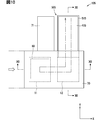
- FIG. 6 is a cross-sectional view taken along the line VII-VII of FIG.
- FIG. 6 is a cross-sectional view taken along the line VIII-VIII of FIG. It is sectional drawing which follows the IX-IX line of FIG.
- the semiconductor device 101 of the first embodiment will be described with reference to FIGS. 1, 2 and 3.
- the semiconductor device 101 includes a first semiconductor element 11, a second semiconductor element 12, a positive electrode metal plate 30, a positive electrode terminal 31, a negative electrode metal plate 40, a negative electrode terminal 41, an output metal plate 70, an output terminal 71, and the like. It can be said that the semiconductor device 101 has a 2in1 package structure.
- the semiconductor device 101 can be applied to, for example, a power conversion device such as an inverter or a converter.
- the negative electrode metal plate 40 corresponds to the first metal plate
- the positive electrode metal plate 30 corresponds to the second metal plate
- the output metal plate 70 corresponds to the third metal plate.
- the positive electrode terminal 31 corresponds to the first terminal
- the negative electrode terminal 41 corresponds to the second terminal.
- the sealing resin portion 20 is composed of electrically insulating members, and covers the semiconductor elements 11 and 12, the positive electrode metal plate 30, the negative electrode metal plate 40, and the output metal plate 70. .. That is, it can be said that the sealing resin portion 20 seals these components while being in contact with these components.
- a semiconductor device 101 in which the first semiconductor element 11 is the upper arm semiconductor element and the second semiconductor element 12 is the lower arm semiconductor element is adopted.
- an RC-IGBT in which an IGBT (Insulated-Gate Bipolar Transistor) and a diode are integrated is adopted as an example of the semiconductor elements 11 and 12.
- the semiconductor elements 11 and 12 are elements having electrodes on both sides.
- the first semiconductor element 11 and the second semiconductor element 12 are semiconductor switching elements.
- MOSFETs can be adopted as the semiconductor elements 11 and 12, or a configuration of a total of four elements in which an IGBT and a diode are arranged one by one in each of the upper and lower arms can be adopted.
- the first semiconductor element 11 and the second semiconductor element 12 are connected in series.
- the collector electrode is electrically connected to the positive electrode terminal 31, and the emitter electrode is electrically connected to the collector electrode of the second semiconductor element 12.
- the collector electrode is electrically connected to the emitter electrode of the first semiconductor element 11, and the emitter electrode is electrically connected to the negative electrode terminal 41.
- the first semiconductor element 11 and the second semiconductor element 12 have a rectangular shape in the XY plane and are arranged side by side in the X direction. Further, as shown in FIGS. 2 and 3, the first semiconductor element 11 and the second semiconductor element 12 have a thickness in the Z direction. Therefore, it can be said that the first semiconductor element 11 and the second semiconductor element 12 have a rectangular parallelepiped shape.
- a collector electrode is formed on one surface, and an emitter electrode is formed on the other surface (opposite surface).
- the first semiconductor element 11 and the second semiconductor element 12 are arranged so that their collector electrodes face the same direction. Therefore, the first semiconductor element 11 and the second semiconductor element 12 are arranged so that their emitter electrodes face the same direction. That is, the first semiconductor element 11 and the second semiconductor element 12 are arranged so that the emitter electrode faces the negative electrode metal plate 40.
- the first semiconductor element 11 is arranged between the negative electrode metal plate 40 and the positive electrode metal plate 30.
- the collector electrode is arranged so as to face the positive electrode metal plate 30.
- the collector electrode is electrically and mechanically connected to the positive electrode metal plate 30 via a conductive connecting member.
- solder is used as an example of the conductive connecting member.
- the conductive connecting member is not limited to solder, and silver paste or the like can also be used.
- the emitter electrode of the first semiconductor element 11 is arranged so as to face the first metal body 62 of the second insulated wiring board 60.
- the emitter electrode is electrically and mechanically connected to the first metal body 62 via solder.
- the emitter electrode is electrically connected to the output metal plate 70 via solder and a first metal body 62.
- the emitter electrode is electrically connected to the collector electrode of the second semiconductor element 12 via the first metal body 62, the solder, and the output metal plate 70.
- the emitter electrode of the first semiconductor element 11 is electrically insulated from the negative electrode metal plate 40 by the second insulating substrate 61 of the second insulated wiring board 60.
- the second insulating substrate 61 corresponds to an insulator.
- the collector electrode of the first semiconductor element 11 corresponds to the electrode on the positive electrode metal plate side.
- the emitter electrode of the first semiconductor element 11 corresponds to an electrode on the negative electrode metal plate side.
- the second insulated wiring board 60 will be described in detail later.
- the second semiconductor element 12 is arranged between the negative electrode metal plate 40 and the output metal plate 70.
- the collector electrode is arranged so as to face the output metal plate 70.
- the collector electrode is electrically and mechanically connected to the output metal plate 70 via solder.
- the emitter electrode is arranged so as to face the negative electrode metal plate 40.
- the emitter electrode is electrically and mechanically connected to the negative electrode metal plate 40 via solder and a terminal 80.
- the collector electrode of the second semiconductor element 12 corresponds to the electrode on the output metal plate side.
- the emitter electrode of the second semiconductor element 12 corresponds to an electrode on the negative electrode metal plate side.
- the terminal 80 is a block body made of a metal such as copper or aluminum.
- the positive electrode metal plate 30 is made of a metal such as copper or aluminum.
- the positive electrode metal plate 30 is, for example, a rectangular parallelepiped block body.
- the positive electrode metal plate 30 which is sufficiently thicker in the Z direction than the semiconductor elements 11 and 12 and has a large area in the XY plane is adopted. Therefore, the semiconductor device 101 can be arranged so that the first semiconductor element 11 fits in the facing region of the positive electrode metal plate 30. Further, the positive electrode metal plate 30 is arranged to face the negative electrode metal plate 40 in the Z direction. Further, it can be said that the positive electrode metal plate 30 is arranged to face the negative electrode metal plate 40 with the first semiconductor element 11 arranged between the positive electrode metal plate 40 and the negative electrode metal plate 40.
- the positive electrode metal plate 30 is electrically and mechanically connected to the positive electrode terminal 31 via solder. Therefore, the positive electrode metal plate 30 has the same potential as the positive electrode terminal 31. Further, the positive electrode metal plate 30 has a function as a part of the current path.
- the positive electrode metal plate 30 Since the positive electrode metal plate 30 is connected to the collector electrode of the first semiconductor element 11 via solder, it can be said that the positive electrode metal plate 30 is thermally connected to the first semiconductor element 11. Therefore, in the positive electrode metal plate 30, the heat generated from the first semiconductor element 11 is transferred via the solder.
- the surface of the positive electrode metal plate 30 opposite to the surface facing the first semiconductor element 11 is exposed from the sealing resin portion 20. Therefore, the positive electrode metal plate 30 can dissipate the heat transferred from the first semiconductor element 11 from the exposed surface exposed from the sealing resin portion 20.
- the positive electrode metal plate 30 has a function as a heat sink.
- the exposed surface is flush with the surrounding sealing resin portion 20 or protrudes from the surrounding sealing resin portion 20.
- the exposed surface can also be said to be a heat dissipation surface.
- the output metal plate 70 is made of the same material as the positive electrode metal plate 30, and has the same thickness as the positive electrode metal plate 30. However, as shown in FIG. 1, the output metal plate 70 is configured as an integral body with the output terminal 71.
- the output metal plate 70 forms, for example, a rectangular parallelepiped block body.
- the output terminal 71 is a portion protruding from a part of the output metal plate 70. Therefore, the output metal plate 70 has the same potential as the output terminal 71. Further, the output metal plate 70 has a function as a part of the current path.
- the output terminal 71 and the output metal plate 70 may be connected to each other with a metal body formed separately by soldering or the like.
- the output metal plate 70 having an area in the XY plane wider than that of the positive electrode metal plate 30 is adopted. More specifically, the output metal plate 70 has the same length in the Y direction as the positive electrode metal plate 30, and is longer in the X direction than the positive electrode metal plate 30. Therefore, the second semiconductor element 12 is provided so as to fit within the facing region of the output metal plate 70. Further, the output metal plate 70 can form a region for connecting the first metal body 62 on the surface facing the second semiconductor element 12.
- the output metal plate 70 is arranged to face the negative electrode metal plate 40 in the Z direction, similarly to the positive electrode metal plate 30.
- the output metal plate 70 is arranged to face the negative electrode metal plate 40 in a state where the second semiconductor element 12 is arranged between the output metal plate 70 and the negative electrode metal plate 40. Further, the output metal plate 70 is arranged side by side with the positive electrode metal plate 30 in the X direction.
- the output metal plate 70 and the positive electrode metal plate 30 are arranged adjacent to each other via the sealing resin portion 20. Therefore, the output metal plate 70 and the positive electrode metal plate 30 are electrically insulated by the sealing resin portion 20.
- the output metal plate 70 Since the output metal plate 70 is connected to the collector electrode of the second semiconductor element 12 via solder, it can be said that the output metal plate 70 is thermally connected to the second semiconductor element 12. Therefore, in the output metal plate 70, the heat generated from the second semiconductor element 12 is transferred via the solder. The surface of the output metal plate 70 opposite to the second semiconductor element 12 is exposed from the sealing resin portion 20. Therefore, the output metal plate 70 can dissipate the heat transferred from the second semiconductor element 12 from the exposed surface exposed from the sealing resin portion 20. As described above, the output metal plate 70 has a function as a heat sink. The exposed surface is flush with the surrounding sealing resin portion 20 or protrudes from the surrounding sealing resin portion 20.
- the negative electrode metal plate 40 is made of the same material as the positive electrode metal plate 30, and has the same shape and thickness as the positive electrode metal plate 30. However, the negative electrode metal plate 40 has a larger area in the XY plane than the positive electrode metal plate 30 and the output metal plate 70. More specifically, the negative electrode metal plate 40 has the same length in the Y direction as the positive electrode metal plate 30 and the output metal plate 70, and is longer in the X direction than the positive electrode metal plate 30 and the output metal plate 70. Further, the length of the negative electrode metal plate 40 in the X direction is longer than the total length of the length of the positive electrode metal plate 30 in the X direction and the length of the output metal plate 70 in the X direction.
- the semiconductor device 101 can be arranged so that both the first semiconductor element 11 and the second semiconductor element 12 are accommodated in the facing region of the negative electrode metal plate 40. Further, the semiconductor device 101 can be arranged so that both the positive electrode metal plate 30 and the output metal plate 70 are accommodated in the facing region of the negative electrode metal plate 40. As described above, the negative electrode metal plate 40 is arranged to face both the first semiconductor element 11 and the second semiconductor element 12.
- the negative electrode metal plate 40 is electrically and mechanically connected to the negative electrode terminal 41 via solder. Therefore, the negative electrode metal plate 40 has the same potential as the negative electrode terminal 41. Further, the negative electrode metal plate 40 has a function as a part of the current path.
- the negative electrode metal plate 40 is connected to the emitter electrode of the second semiconductor element 12 via solder, it can be said that the negative electrode metal plate 40 is thermally connected to the second semiconductor element 12. Further, the negative electrode metal plate 40 is connected to the second metal body 63 of the second insulated wiring board 60 via solder. In the second insulated wiring board 60, the emitter electrode of the first semiconductor element 11 is connected to the first metal body 62. As will be described later, the first metal body 62 and the second metal body 63 are metal bodies formed on the front and back surfaces of the second insulating substrate 61. The heat generated by the first semiconductor element 11 is transferred to the negative electrode metal plate 40 via the second insulated wiring board 60.
- the negative electrode metal plate 40 is thermally connected to the emitter electrode of the first semiconductor element 11 by the second insulating substrate 61 in a state of being electrically insulated. Therefore, the heat generated from the first semiconductor element 11 and the heat generated from the second semiconductor element 12 are transferred to the negative electrode metal plate 40.
- the negative electrode metal plate 40 has a function as a heat sink.
- the positive electrode terminal 31 and the negative electrode terminal 41 are terminals for electrically connecting a device or circuit provided outside the semiconductor device 101 and the semiconductor device 101. That is, the electrode terminal 31 and the negative electrode terminal 41 are terminals for external connection.
- the positive electrode terminal 31 and the negative electrode terminal 41 are arranged to face each other. As shown in FIGS. 1 and 2, the positive electrode terminals 31 are arranged at positions biased toward the first semiconductor element 11 with respect to the second semiconductor element 12. It can be said that the positive electrode terminal 31 is arranged adjacent to the first semiconductor element 11 in the Y direction. In other words, the positive electrode terminal 31 is arranged side by side with the first semiconductor element 11 in the Y direction of the XY plane.
- the negative electrode terminal 41 is a terminal through which a current flows between the negative electrode terminal 41 and the positive electrode terminal 31, and is arranged so as to face the positive electrode terminal 31. Therefore, the negative electrode terminal 41 is arranged on the Y direction side with respect to the first semiconductor element 11 in the XY plane.
- the positive electrode terminal 31 and the negative electrode terminal 41 are arranged so as to face each other with the first insulating substrate 51, which is an electrically insulating member, arranged between them in order to electrically insulate them from each other. Further, in the present embodiment, as an example, the positive electrode terminal 31 and the negative electrode terminal 41, which are made of metal bodies formed on the front and back surfaces of the first insulating substrate 51, are adopted. That is, the positive electrode terminal 31 and the negative electrode terminal 41 are metal bodies formed on the front and back surfaces of the first insulated substrate 51 in the first insulated wiring board 50.
- the first insulating substrate 51 corresponds to an insulating plate.
- the first insulated wiring board 50 is a substrate in which a positive electrode terminal 31 and a negative electrode terminal 41 are formed of a metal body such as copper on the front and back surfaces of a first insulated substrate 51 made of ceramics such as silicon nitride and integrated. is there. That is, in the first insulated wiring board 50, the metal body formed on one surface of the first insulated substrate 51 includes the positive electrode terminal 31, and the metal body formed on the other surface of the first insulated substrate 51 is formed.
- the negative electrode terminal 41 is included.
- the positive electrode terminal 31 and the negative electrode terminal 41 are formed, for example, by patterning a metal body formed on the first insulating substrate 51.
- One end of the first insulated wiring board 50 is arranged in the facing region between the positive electrode plate 30 and the negative electrode plate 40, and the other parts are arranged outside the facing region. Since the first insulated wiring board 50 uses ceramics as the first insulated substrate 51, it has good thermal conductivity.
- the positive electrode terminal 31, the first insulated board 51, and the negative electrode terminal 41 can be configured by one component. Further, in the semiconductor device 101, the positive electrode terminal 31 and the negative electrode terminal 41 are arranged so as to face each other (arranged in parallel) while ensuring the electrical insulation between the positive electrode terminal 31 and the negative electrode terminal 41 by the first insulating substrate 51. be able to.
- the first insulated wiring board 50 is partially covered with the sealing resin portion 20, and the other portions are exposed from the sealing resin portion 20.
- the electrode terminal 31 and the negative electrode terminal 41 are exposed from the sealing resin portion 20.
- the electrode terminal 31 and the negative electrode terminal 41 may not be arranged to face each other. Further, in the present disclosure, the positive electrode terminal 31 may not be arranged at a position biased toward the first semiconductor element 11 with respect to the second semiconductor element 12.
- the second insulated wiring board 60 is integrated with the first metal body 62 and the second metal body 63 formed of a metal body such as copper on the front and back surfaces of the second insulated board 61 made of ceramics such as silicon nitride. It is a board that has been made.
- the metal body formed on one surface of the second insulated substrate 61 includes the first metal body 62, and the metal body formed on the other surface of the second insulated substrate 61 is included. It contains a second metal body 63.
- the first metal body 62 and the second metal body 63 are electrically insulated by the second insulating substrate 61.
- the first metal body 62 and the second metal body 63 are formed, for example, by patterning a metal body formed on the second insulating substrate 61.
- the second insulated wiring board 60 is arranged at a position facing the first semiconductor element 11 and a position facing the end of the output metal plate 70. That is, the second insulated wiring board 60 is provided from above the first semiconductor element 11 to above the end of the output metal plate 70. Further, the first metal body 62 is arranged at a position facing the first semiconductor element 11 and a position facing the end portion of the output metal plate 70. The emitter electrode of the first semiconductor element 11 and the output metal plate 70 are electrically connected to the first metal body 62. On the other hand, the second metal body 63 is electrically connected to the negative electrode plate 40.
- the second insulated wiring board 60 has good thermal conductivity because ceramics are used as the second insulated board 61. Therefore, the heat generated from the first semiconductor element 11 is easily transferred to the negative electrode plate 40 via the solder and the second insulated wiring board 60. Therefore, it can be said that the emitter electrode of the first semiconductor element 11 is thermally connected to the negative electrode metal plate 40 in a state of being electrically insulated from the negative electrode metal plate 40 by the second insulating substrate 61. However, the heat generated by the first semiconductor element 11 is transferred to the negative electrode metal plate 40 even if ceramics are not used as the second insulating substrate 61.
- the first metal body 62 corresponds to a connecting portion that electrically connects the emitter electrode and the output metal plate 70 in the first semiconductor element 11.
- the first metal body 62 includes a recess 62a having a recessed portion between the facing portion facing the emitter electrode and the facing portion facing the output metal plate 70. .. That is, the recess 62a is a portion of the first metal body 62 whose thickness in the Z direction is thinner than that of the periphery.
- the recess 62a is provided at a position facing the entire area in the Y direction at least at the end of the first semiconductor element 11. As a result, the first metal body 62 can easily secure an insulation distance from the collector electrode of the first semiconductor element 11 and the positive electrode metal plate 30.
- FIGS. 2 and 3 The broken line arrows in FIGS. 2 and 3 indicate a schematic current flow (current path) between the positive electrode terminal and the negative electrode terminal. Since the direction of the current depends on the operating state of the inverter, it is not always the direction from the positive electrode to the negative electrode.
- the semiconductor device 101 a current flows from the positive electrode terminal 31 to the negative electrode terminal 41. More specifically, the semiconductor device 101 includes a positive electrode terminal 31, a positive electrode metal plate 30, a first semiconductor element 11, a first metal body 62, an output metal plate 70, a second semiconductor element 12, a terminal 80, a negative electrode metal plate 40, and a negative electrode. A current path through which current flows is formed in the order of the terminals 41. It can be said that the semiconductor device 101 has an N-shaped connection structure. Further, in the semiconductor device 101, a current also flows through the solder that electrically connects each component. However, it is omitted here for the sake of brevity.
- the current path from the positive electrode terminal 31 to the positive electrode metal plate 30 is arranged to face the current path from the negative electrode metal plate 40 to the negative electrode terminal 41, and the directions of the currents are opposite to each other. It is oriented. Further, in the semiconductor device 101, as shown in FIG. 3, the current path from the positive electrode metal plate 30 to the output metal plate 70 is arranged to face the current path of the negative electrode metal plate 40, and the direction of the current is opposite. There is. More specifically, in the semiconductor device 101, the current path from the positive electrode metal plate 30 to the output metal plate 70 via the first metal body 62 is arranged to face the current path from the negative electrode metal plate 40 to the second metal body 63. The direction of the current is opposite.
- the current paths are arranged to face each other, the section in which the current direction is opposite can be increased, and the inductance of the wiring can be reduced. Further, in the present disclosure, since the inductance can be reduced without using the intermediate electrode, it is possible to suppress the increase in physique. Further, it can be said that the semiconductor device 101 can make the current loop small and have excellent electrical characteristics.
- the present disclosure has been described above. However, the present disclosure is not limited to the above-described embodiment, and various modifications can be made without departing from the gist of the present disclosure.
- the second to fifth embodiments and the modified examples 1 to 7 will be described.
- the above-described embodiment, the second to fifth embodiments, and the modified examples 1 to 7 can be carried out individually, but can also be carried out in combination as appropriate.
- the present disclosure is not limited to the combinations shown in the embodiments, but can be implemented by various combinations.
- the semiconductor device 102 of the second embodiment will be described with reference to FIG.
- the semiconductor device 102 is different from the semiconductor device 101 in that the first insulated wiring board 50 is not used. Similar to the semiconductor device 101, the semiconductor device 102 has an N-shaped connection structure. Note that FIG. 4 is a cross-sectional view corresponding to FIG.
- the semiconductor device 102 includes a metal member in which the positive electrode metal plate 302 and the positive electrode terminal 312 are integrally formed, and a metal member in which the negative electrode metal plate 402 and the negative electrode terminal 412 are integrally formed.
- the positive electrode terminal 312 and the negative electrode terminal 412 are arranged so as to face each other, and are electrically insulated by the sealing resin portion 202.
- the semiconductor device 102 can exert the same effect as the semiconductor device 101. Further, in the semiconductor device 102, the positive electrode terminal 312 and the negative electrode terminal 412 are electrically insulated by the sealing resin portion 202. Therefore, the semiconductor device 102 can have a longer insulation distance between the positive electrode terminal 312 and the negative electrode terminal 412 than the semiconductor device 101. Further, the semiconductor device 102 does not require the first insulated wiring board 50, and has an advantage that the cost can be reduced as compared with the semiconductor device 101.
- the semiconductor device 103 of the third embodiment will be described with reference to FIG.
- the semiconductor device 103 is different from the semiconductor device 101 in that it mainly uses an insulated wiring board 503. Similar to the semiconductor device 101, the semiconductor device 103 has an N-shaped connection structure. Note that FIG. 5 is a cross-sectional view corresponding to FIG.
- the metal body formed on one surface of the insulating substrate 513 includes the first metal body 62 and the positive electrode terminal 313, and the metal body formed on the other surface of the insulating substrate 513 is the negative electrode terminal. 413 is included.
- the negative electrode terminal 413 can be regarded as one in which the second metal body 63 of the first embodiment and the negative electrode terminal 41 are integrated.
- the insulated wiring board 503 can be made of the same material as the first insulated wiring board 50 and the second insulated wiring board 60, and can be manufactured by the same method. As described above, the insulated wiring board 503 corresponds to a board in which the first insulated wiring board 50 and the second insulated wiring board 60 are integrally formed.
- the insulating substrate 513 corresponds to an insulator.
- the semiconductor device 103 can exert the same effect as the semiconductor device 101. Further, since the semiconductor device 103 has the insulating wiring board 503, the insulating substrate 513, the first metal body 62, the positive electrode terminal 313, and the negative electrode terminal 413 can be integrated. Further, the semiconductor device 103 does not need to use two insulated wiring boards, a first insulated wiring board 50 and a second insulated wiring board 60.
- the semiconductor device 104 of the fourth embodiment will be described with reference to FIGS. 6 to 9.
- the semiconductor device 104 is different from the semiconductor device 101 in that it mainly uses an insulated wiring board 504. Similar to the semiconductor device 101, the semiconductor device 104 has an N-shaped connection structure. In this embodiment, the sealing resin portion 20 is not shown in order to prevent the drawings from becoming complicated.
- the semiconductor device 104 includes an insulated wiring board 504, a first signal terminal S1, and a second signal terminal S2.
- the insulated wiring board 504 includes a metal body formed on one surface of the insulating substrate 514 and a metal body formed on the other surface of the insulating substrate 514.
- the insulated wiring board 504 can be made of the same material as the first insulated wiring board 50 and the second insulated wiring board 60, and can be manufactured by the same method.
- the metal body formed on one surface of the insulating substrate 514 includes a metal body for signal 524 in addition to the first metal body 62 and the positive electrode terminal. I'm out.
- the positive electrode terminal of the semiconductor device 104 has the same configuration as the positive electrode terminal 313 of the semiconductor device 103.
- the insulating substrate 514 is provided with a plurality of signal metal bodies 524. As shown in FIG. 7, the signal metal body 524 is electrically connected to, for example, the gate electrodes of the semiconductor elements 11 and 12, and is also electrically connected to the signal terminals S2 (S1).
- the semiconductor device 104 may include a temperature-sensitive diode for detecting the temperatures of the semiconductor elements 11 and 12.
- the signal terminals S1 and S2 may include those electrically connected to the temperature sensitive diode.
- the insulating substrate 514 is provided with a plurality of signal metal bodies 524 arranged in the X direction along the Y direction. Further, the insulating substrate 514 is provided with a plurality of signal metal bodies 524 on the side opposite to the positive electrode terminal with the first semiconductor element 11 as a reference. Further, the insulating substrate 514 is provided with a plurality of signal metal bodies 524 on the opposite side of the output terminal 71 with reference to the second semiconductor element 12. That is, on one surface of the insulating substrate 514, the signal metal body 524, the first metal body 62, and the positive electrode terminal are arranged side by side in this order in the Y direction, and the signal metal body 524 and the connection metal body are arranged. The 534s are arranged side by side in this order.
- the metal body formed on the other surface of the insulating substrate 514 includes the negative electrode terminal 414 as shown in FIGS. 8 and 9. Like the negative electrode terminal 413, the negative electrode terminal 414 is arranged to face the positive electrode terminal. The negative electrode terminal 414 and the positive electrode terminal are electrically insulated by the insulating substrate 514.
- the metal body as the negative electrode terminal 414 is provided from the facing region of the first semiconductor element 11 to the facing region of the second semiconductor element 12 in addition to the position protruding from the sealing resin portion 20, and is integrally provided. ing.
- the negative electrode terminal 414 is provided integrally with the connecting metal body 534.
- the insulating substrate 514 has a through hole 514a formed at a position facing the second semiconductor element 12.
- the connecting metal body 534 is provided in the through hole 514a, and is provided over one surface side and the other surface side of the insulating substrate 514.
- the negative electrode terminal 414 and the connecting metal body 534 are electrically and mechanically connected to the negative electrode metal plate 40 via solder. Further, the connecting metal body 534 is electrically and mechanically connected to the emitter electrode of the second semiconductor element 12 via solder. As a result, the emitter electrode of the second semiconductor element 12 is electrically connected to the negative electrode terminal 414.
- the semiconductor device 104 can exert the same effect as the semiconductor device 101. Further, in the semiconductor device 104, since the insulated wiring board 504 can be evenly arranged on the left and right sides on the XY plane, stress balance can be easily obtained. That is, the semiconductor device 104 can suppress the local generation of stress due to the difference in the coefficient of linear expansion between the components. More specifically, the semiconductor device 104 can suppress the generation of stress in the semiconductor elements 11 and 12 and each connection portion. Therefore, the semiconductor device 104 can improve the electrical reliability as compared with the case where the stress is locally generated.
- the insulated wiring board 504 has a signal metal body 524 in addition to the first metal body 62 and the connection metal body 534. Therefore, the semiconductor device 104 can connect the insulated wiring board 504 to the first signal terminal S1 and the second signal terminal S2 at the same time as connecting the insulated wiring board 504 to the semiconductor elements 11 and 12.
- the semiconductor device 105 of the fifth embodiment will be described with reference to FIGS. 10 to 12.
- the semiconductor device 105 mainly differs from the semiconductor device 101 in the arrangement of the semiconductor elements 11 and 12.
- the semiconductor device 105 has a U-shaped connection structure.
- the sealing resin portion 20 is not shown in order to prevent the drawings from becoming complicated.
- the semiconductor device 105 includes a first semiconductor element 11 as an upper arm semiconductor element and a second semiconductor element 12 as a lower arm semiconductor element connected in series with the first semiconductor element.
- the first semiconductor element 11 and the second semiconductor element 12 are arranged in opposite directions.
- the semiconductor elements 11 and 12 are arranged so that the emitter electrode of the first semiconductor element 11 and the collector electrode of the second semiconductor element 12 face the same direction. Therefore, the semiconductor elements 11 and 12 are arranged so that the collector electrode of the first semiconductor element 11 and the emitter electrode of the second semiconductor element 12 face the same direction.
- the emitter electrode of the first semiconductor element 11 and the collector electrode of the second semiconductor element 12 are arranged to face the output metal plate 70. Further, in the semiconductor device 105, the collector electrode of the first semiconductor element 11 and the emitter electrode of the second semiconductor element 12 are arranged to face the positive electrode metal plate 30.
- the semiconductor device 105 includes an insulated wiring board 505.
- the insulated wiring board 505 is a substrate in which a metal body such as copper is formed on the front and back surfaces of an insulating substrate 515 made of ceramics such as silicon nitride and integrated. ..
- the insulated wiring board 505 is provided from the facing region of the second semiconductor element 12 to the outside of the sealing resin portion 20.
- the positive electrode terminal 315 and the negative electrode terminal 415 which will be described later, can be used as external connection terminals.
- the metal body formed on one surface of the insulated substrate 515 includes the positive electrode terminal 315
- the metal body formed on the other surface of the insulated substrate 515 includes the negative electrode terminal 415.
- the positive electrode terminal 315 and the negative electrode terminal 415 are formed on the insulated wiring board 505, similarly to the semiconductor device 103. Therefore, the positive electrode terminal 315 and the negative electrode terminal 415 are arranged to face each other via the insulating substrate 515, and are electrically insulated by the insulating substrate 515.
- the insulated wiring board 505 is arranged at a position biased toward the second semiconductor element with respect to the first semiconductor element. Therefore, the positive electrode terminal 315 and the negative electrode terminal 415 are arranged at positions biased toward the second semiconductor element 12 with respect to the first semiconductor element 11. That is, the positive electrode terminal 315 and the negative electrode terminal 415 are arranged side by side with the second semiconductor element 12 in the Y direction of the XY plane.
- the positive electrode metal plate 30 and the output metal plate 70 are arranged to face each other.
- the positive electrode metal plate 30 and the output metal plate 70 have the same material and the same shape as those of the first embodiment. However, in the present embodiment, unlike the first embodiment, the positive electrode metal plate 30 and the output metal plate 70 have the same physique.
- the positive electrode metal plate 30 corresponds to the first metal plate.
- the output metal plate 70 corresponds to the second metal plate.
- the positive electrode metal plate 30 is arranged to face both the first semiconductor element 11 and the second semiconductor element 12, and is electrically connected to the positive electrode terminal 315.
- the positive electrode metal plate 30 is electrically and mechanically connected to the positive electrode terminal 315 via solder.
- the positive electrode terminal 315 and the negative electrode terminal 415 may not be arranged at positions biased toward the second semiconductor element 12 with respect to the first semiconductor element 11. Further, in the present disclosure, the positive electrode terminal 315 and the negative electrode terminal 415 may not be arranged to face each other.
- the output metal plate 70 is arranged to face both the first semiconductor element 11 and the second semiconductor element 12 in a state where the first semiconductor element 11 and the second semiconductor element 12 are arranged between the positive metal plate 30 and the positive metal plate 30. There is. As shown in FIG. 10, the output metal plate 70 is provided with an output terminal 71.
- the sealing resin portion 20 covers the first semiconductor element 11, the second semiconductor element 12, the positive electrode metal plate 30, and the output metal plate 70, as in the first embodiment. Then, in the positive electrode metal plate 30 and the output metal plate 70, the opposite surfaces of the surfaces facing the first semiconductor element 11 and the second semiconductor element 12 are exposed from the sealing resin portion 20.
- the emitter electrode which is an electrode on the output metal plate 70 side, is electrically connected to the output metal plate 70. More specifically, the emitter electrode of the first semiconductor element 11 is electrically and mechanically connected to the terminal 80 via solder. The terminal 80 is electrically and mechanically connected to the output metal plate 70 via solder.
- the collector electrode which is the electrode on the positive electrode metal plate 30 side, is electrically connected to the positive electrode metal plate 30 via solder.
- the positive electrode metal plate 30 is electrically connected to the positive electrode terminal 315 as described above. Therefore, the collector electrode of the first semiconductor element 11 is electrically connected to the positive electrode metal plate 30 via the positive electrode metal plate 30.
- the collector electrode which is the electrode on the output metal plate 70 side
- the emitter electrode which is an electrode on the positive electrode metal plate 30 side
- the negative electrode terminal 415 is electrically insulated from the positive electrode terminal 315 and the positive electrode metal plate 30 by the insulating substrate 515. Therefore, the emitter electrode of the second semiconductor element 12 is thermally connected to the positive electrode metal plate 30 by the insulating substrate 515 in a state of being electrically insulated.
- FIGS. 10 to 12 The broken line arrows in FIGS. 10 to 12 indicate a schematic current flow (current path).
- a current flows from the positive electrode terminal 315 to the negative electrode terminal 415. More specifically, the semiconductor device 105 has a current path in which current flows in the order of the positive electrode terminal 315, the positive electrode metal plate 30, the first semiconductor element 11, the terminal 80, the output metal plate 70, the second semiconductor element 12, and the negative electrode terminal 415. It is formed.
- the current path of the positive electrode terminal 315 faces the current path of the negative electrode terminal 415, and the current flows in the opposite direction. Further, in the current path of the positive electrode metal plate 30, a current flows in the opposite direction to the current path of the output metal plate 70. Therefore, the semiconductor device 105 can exert the same effect as the semiconductor device 101.
- the semiconductor device 101 By the way, for example, in the semiconductor device 101, two metal plates, a positive electrode metal plate 30 and an output metal plate 70, are arranged on one side facing the semiconductor elements 11 and 12. Therefore, the semiconductor device 101 needs to secure insulation between the positive electrode metal plate 30 and the output metal plate 70. Therefore, in the semiconductor device 101, the positive electrode metal plate 30 and the output metal plate 70 are arranged apart from each other. That is, the semiconductor device 101 requires an insulating space for insulating the positive electrode metal plate 30 and the output metal plate 70.
- the positive electrode metal plate 30 is arranged on one side facing each of the semiconductor elements 11 and 12, and the output metal plate 70 is arranged on the other side.
- the metal plates are not arranged in the X direction, it is not necessary to secure the insulation between the metal plates arranged in the X direction.
- the semiconductor device 105 can be made smaller than the semiconductor device 101 because it does not require an insulating space.
- the alternate long and short dash line in FIG. 10 shows the difference in body size between the semiconductor device 101 and the semiconductor device 105 in the X direction.
- FIG. 13 is a cross-sectional view corresponding to FIG.
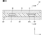
- the semiconductor device 106 includes a connecting member 606 made of the same material as the positive electrode metal plate 30 and the like.
- the connecting member 606 is a member that electrically connects the emitter electrode of the first semiconductor element 11 and the output metal plate 70. That is, the semiconductor device 106 includes a connecting member 606 instead of the first metal body 62.
- the sealing resin portion 206 covers the semiconductor elements 11, 12, and the like, similarly to the sealing resin portion 20.
- the sealing resin portion 206 includes an intervening portion 206a formed between the connecting member 606 and the negative electrode metal plate 40.
- the connecting member 606 and the negative electrode metal plate 40 are electrically insulated by the intervening portion 206a. That is, the emitter electrode of the first semiconductor element 11 is electrically insulated from the negative electrode metal plate 40 by the intervening portion 206a.
- the thickness of the intervening portion 206a may be such that the connecting member 606 and the negative electrode metal plate 40 can be electrically insulated, and the heat generated by the first semiconductor element 11 is transferred to the negative electrode metal plate 40. Further, the thickness of the intervening portion 206a is as thin as possible within the range where the connecting member 606 and the negative electrode metal plate 40 can be electrically insulated, and the heat generated by the first semiconductor element 11 is transferred to the negative electrode metal plate 40. It is preferable because it is easy.
- the intervening portion 206a corresponds to an insulator.
- the semiconductor device 106 can exert the same effect as the semiconductor device 101. Further, the semiconductor device 106 can secure the electrical insulation property by the sealing resin portion 206 without providing the insulating wiring board.
- FIG. 14 is a cross-sectional view corresponding to FIG.
- FIG. 15 is a cross-sectional view corresponding to FIG.
- the semiconductor device 107 includes a metal member in which a positive electrode metal plate 307 and a positive electrode terminal 317 are integrally formed, and a metal member in which a negative electrode metal plate 407 and a negative electrode terminal 417 are integrally formed. And have. These metal members are made of the same material as the positive electrode metal plate 30 and the like.
- the negative electrode metal plate 407 is arranged to face the emitter electrode of the second semiconductor element 12, and is electrically connected to the emitter electrode of the second semiconductor element 12 via solder. Further, in the negative electrode metal plate 407, the opposite surface of the surface of the second semiconductor element 12 facing the emitter electrode faces the positive electrode metal plate 307.
- the sealing resin portion 207 covers the semiconductor elements 11 and 12 and the like, similarly to the sealing resin portion 20.
- the sealing resin portion 207 includes an intervening portion 207a formed between the positive electrode metal plate 307 and the negative electrode metal plate 407.
- the positive electrode metal plate 307 and the negative electrode metal plate 407 are electrically insulated by the intervening portion 207a. That is, in the second semiconductor element 12, the emitter electrode is electrically connected to the negative electrode metal plate 407, and the second semiconductor element 12 is electrically insulated from the positive electrode metal plate 307 by the intervening portion 207a.
- the thickness of the intervening portion 207a may be such that the positive electrode metal plate 307 and the negative electrode metal plate 407 can be electrically insulated and the heat generated by the second semiconductor element 12 is transferred to the positive electrode metal plate 307. .
- the thickness of the intervening portion 207a is as thin as possible within the range where the positive electrode metal plate 307 and the negative electrode metal plate 407 can be electrically insulated, and the heat generated by the second semiconductor element 12 is transferred to the positive electrode metal plate 307. It is preferable because it is easy to be used.
- the intervening portion 207a corresponds to an insulator.
- the semiconductor device 107 can exert the same effect as the semiconductor device 101. Further, the semiconductor device 107 can secure the electrical insulation property by the sealing resin portion 207 without providing the insulating wiring board.
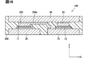
- FIG. 16 is a cross-sectional view corresponding to FIG.
- the connecting member 606 and the negative electrode metal plate 40 are mechanically connected by the insulating adhesive 208a.
- the connecting member 606 and the negative electrode metal plate 40 are electrically insulated by the insulating adhesive 208a. That is, the emitter electrode of the first semiconductor element 11 is electrically insulated from the negative electrode metal plate 40 by the insulating adhesive 208a.
- the insulating adhesive 208a corresponds to an insulator.
- the insulating adhesive 208a is preferable because the higher the thermal conductivity, the easier it is to thermally connect the emitter electrode of the first semiconductor element 11 and the negative electrode metal plate 40. That is, the insulating adhesive 208a is preferable because the higher the thermal conductivity, the easier it is for the heat generated by the first semiconductor element 11 to be transferred to the negative electrode metal plate 40.
- the semiconductor device 108 can exert the same effect as the semiconductor device 106. Further, the semiconductor device 108 electrically insulates the connecting member 606 and the negative electrode metal plate 40 with the sealing resin portion 206 and the insulating adhesive 208a of another member. Therefore, the semiconductor device 108 is easier to adjust the ease of heat transfer between the emitter electrode of the first semiconductor element 11 and the negative electrode metal plate 40 than the semiconductor device 106.
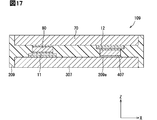
- FIG. 17 is a cross-sectional view corresponding to FIG.
- the positive electrode metal plate 307 and the negative electrode metal plate 407 are mechanically connected by an insulating adhesive 209a.
- the positive electrode metal plate 307 and the negative electrode metal plate 407 are electrically insulated by the insulating adhesive 209a. That is, the emitter electrode of the second semiconductor element 12 is electrically insulated from the positive electrode metal plate 307 by the insulating adhesive 209a.
- the insulating adhesive 209a is an insulating adhesive 208a and corresponds to an insulator.
- the semiconductor device 109 can exert the same effect as the semiconductor device 107. Further, the semiconductor device 109 electrically insulates the positive electrode metal plate 307 and the negative electrode metal plate 407 with the sealing resin portion 209 and the insulating adhesive 209a of another member. Therefore, the semiconductor device 109 is easier to adjust the ease of heat transfer between the emitter electrode of the second semiconductor element 12 and the positive electrode metal plate 307 than the semiconductor device 107.
- the semiconductor device described so far may be attached to the coolers 1010 and 1020. Therefore, with reference to FIGS. 18, 19, and 20, modifications 5, 6 and 7 will be described as an example of a configuration in which the semiconductor device is attached to the coolers 1010 and 1020.
- the structure in which the semiconductor device is attached to the coolers 1010 and 1020 can be said to be a semiconductor module.
- the coolers 1010 and 1020 for example, those described in JP-A-2018-101666 can be adopted.
- the modified example 5 has a configuration in which the semiconductor device 101 is attached to the first cooler 1010 and the second cooler 1020.
- FIG. 18 is a cross-sectional view corresponding to FIG.
- the first cooler 1010 and the second cooler 1020 are made of a metal such as copper or aluminum, and a flow path through which a refrigerant such as cooling water flows is formed.
- the semiconductor device 101 is sandwiched between the first cooler 1010 and the second cooler 1020.
- the first insulator 1030, the first outer surface metal body 1040, and the first cooler 1010 are laminated and arranged in this order on the negative electrode metal plate 40 side.
- the negative electrode metal plate 40 and the first insulator 1030 are in contact with each other, the first insulator 1030 and the first outer surface metal body 1040 are in contact with each other, and the first outer surface metal body 1040 and the first cooler 1010 are in contact with each other. Is in contact.
- the negative electrode metal plate 40 and the first cooler 1010 are electrically insulated by the first insulator 1030.
- the negative electrode metal plate 40, the first insulator 1030, and the first outer surface metal body 1040 may be formed of an insulated wiring substrate.
- the first insulator 1030, the first outer surface metal body 1040, and the first cooler 1010 are laminated and arranged in this order on the negative electrode metal plate 40 side. Therefore, in the semiconductor device 101, the negative electrode metal plate 40 and the first cooler 1010 are electrically insulated by the first insulator 1030.
- the negative electrode metal plate 40, the first insulator 1030, and the first outer surface metal body 1040 may be formed of an insulated wiring substrate.
- the second insulator 1050, the second outer surface metal body 1060, and the second cooler 1020 are laminated and arranged in this order on the positive electrode metal plate 30 and the output metal plate 70 side.
- the positive electrode metal plate 30 and the output metal plate 70 are in contact with the second insulator 1050
- the second insulator 1050 and the second outer surface metal body 1060 are in contact with each other
- the second outer surface metal body 1060 and the second insulator are in contact with each other. 2 It is in contact with the cooler 1020.
- the positive electrode metal plate 30, the output metal plate 70, and the second cooler 1020 are electrically insulated by the second insulator 1050.
- the positive electrode metal plate 30, the output metal plate 70, the second insulator 1050, and the second outer surface metal body 1060 may be formed of an insulated wiring substrate.
- the semiconductor device 101 can be cooled by the coolers 1010 and 1020 while being electrically insulated from the coolers 1010 and 1020.
- the modification 6 has a configuration in which the semiconductor device 104 is attached to the first cooler 1010 and the second cooler 1020.
- FIG. 19 is a cross-sectional view corresponding to FIGS. 8 and 9.
- the semiconductor device 104 is different from the semiconductor module of the modification 5. Therefore, the semiconductor module of the modification 6 can exert the same effect as the modification 5.
- the modification 7 has a configuration in which the semiconductor device 105 is attached to the first cooler 1010 and the second cooler 1020.
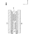
- FIG. 20 is a cross-sectional view corresponding to FIG.
- the semiconductor device 105 is different from the semiconductor module of the modification 5. Therefore, the semiconductor module of the modification 7 can have the same effect as that of the modification 5.
Landscapes
- Engineering & Computer Science (AREA)
- Power Engineering (AREA)
- Microelectronics & Electronic Packaging (AREA)
- General Physics & Mathematics (AREA)
- Condensed Matter Physics & Semiconductors (AREA)
- Computer Hardware Design (AREA)
- Physics & Mathematics (AREA)
- Chemical & Material Sciences (AREA)
- Materials Engineering (AREA)
- Ceramic Engineering (AREA)
- Cooling Or The Like Of Semiconductors Or Solid State Devices (AREA)
- Structures Or Materials For Encapsulating Or Coating Semiconductor Devices Or Solid State Devices (AREA)
- Inverter Devices (AREA)
Abstract
La présente invention concerne un dispositif à semi-conducteur comportant : une plaque métallique d'électrode négative (40) disposée de manière à faire face à la fois à un premier élément semi-conducteur (11) et à un second élément semi-conducteur (12) ; une plaque métallique d'électrode positive (30) disposée de manière à faire face à la plaque métallique d'électrode négative de telle sorte que le premier élément semi-conducteur est disposé entre la plaque métallique d'électrode positive et la plaque métallique d'électrode négative ; et une plaque métallique de sortie (70) disposée de manière à faire face à la plaque métallique d'électrode négative de telle sorte que le second élément semi-conducteur est disposé entre la plaque métallique de sortie et la plaque métallique d'électrode négative. Concernant le second élément semi-conducteur, une électrode collectrice est électriquement connectée à la plaque métallique de sortie, et une électrode d'émetteur est électriquement connectée à la plaque métallique d'électrode négative. Concernant le premier élément semi-conducteur, une électrode collectrice est électriquement connectée à la plaque métallique d'électrode positive, une électrode d'émetteur est électriquement connectée à la plaque métallique de sortie, et le premier élément semi-conducteur est thermiquement connecté à la plaque métallique d'électrode négative au moyen d'un second substrat isolé (61) dans un état électriquement isolé.
Priority Applications (2)
| Application Number | Priority Date | Filing Date | Title |
|---|---|---|---|
| CN202080021731.8A CN113597671B (zh) | 2019-03-19 | 2020-02-05 | 半导体装置 |
| US17/475,102 US11990391B2 (en) | 2019-03-19 | 2021-09-14 | Semiconductor device |
Applications Claiming Priority (2)
| Application Number | Priority Date | Filing Date | Title |
|---|---|---|---|
| JP2019-051427 | 2019-03-19 | ||
| JP2019051427A JP7088094B2 (ja) | 2019-03-19 | 2019-03-19 | 半導体装置 |
Related Child Applications (1)
| Application Number | Title | Priority Date | Filing Date |
|---|---|---|---|
| US17/475,102 Continuation US11990391B2 (en) | 2019-03-19 | 2021-09-14 | Semiconductor device |
Publications (1)
| Publication Number | Publication Date |
|---|---|
| WO2020189065A1 true WO2020189065A1 (fr) | 2020-09-24 |
Family
ID=72520703
Family Applications (1)
| Application Number | Title | Priority Date | Filing Date |
|---|---|---|---|
| PCT/JP2020/004299 WO2020189065A1 (fr) | 2019-03-19 | 2020-02-05 | Dispositif à semi-conducteur |
Country Status (4)
| Country | Link |
|---|---|
| US (1) | US11990391B2 (fr) |
| JP (1) | JP7088094B2 (fr) |
| CN (1) | CN113597671B (fr) |
| WO (1) | WO2020189065A1 (fr) |
Citations (2)
| Publication number | Priority date | Publication date | Assignee | Title |
|---|---|---|---|---|
| JP2014011338A (ja) * | 2012-06-29 | 2014-01-20 | Denso Corp | 半導体装置 |
| JP2015185749A (ja) * | 2014-03-25 | 2015-10-22 | トヨタ自動車株式会社 | 半導体モジュール |
Family Cites Families (16)
| Publication number | Priority date | Publication date | Assignee | Title |
|---|---|---|---|---|
| JP2002164502A (ja) * | 2000-11-28 | 2002-06-07 | Unisia Jecs Corp | 半導体装置 |
| JP2003078093A (ja) * | 2001-09-05 | 2003-03-14 | Hitachi Unisia Automotive Ltd | 半導体装置 |
| JP3922698B2 (ja) * | 2002-07-26 | 2007-05-30 | 株式会社日立製作所 | 半導体装置 |
| JP4532303B2 (ja) | 2005-02-08 | 2010-08-25 | トヨタ自動車株式会社 | 半導体モジュール |
| JP4564937B2 (ja) | 2006-04-27 | 2010-10-20 | 日立オートモティブシステムズ株式会社 | 電気回路装置及び電気回路モジュール並びに電力変換装置 |
| DE112009005537B3 (de) * | 2008-04-09 | 2022-05-12 | Fuji Electric Co., Ltd. | Verfahren zum Herstellen einer Halbleitervorrichtung |
| JP5701377B2 (ja) * | 2011-03-24 | 2015-04-15 | 三菱電機株式会社 | パワー半導体モジュール及びパワーユニット装置 |
| JP5947537B2 (ja) | 2011-04-19 | 2016-07-06 | トヨタ自動車株式会社 | 半導体装置及びその製造方法 |
| JP5664475B2 (ja) * | 2011-06-22 | 2015-02-04 | 株式会社デンソー | 半導体装置 |
| CN104412383B (zh) | 2012-06-29 | 2017-09-26 | 株式会社电装 | 半导体装置以及半导体装置的连接构造 |
| JP6114149B2 (ja) * | 2013-09-05 | 2017-04-12 | トヨタ自動車株式会社 | 半導体装置 |
| CN106030796B (zh) * | 2014-02-11 | 2018-07-06 | 三菱电机株式会社 | 功率用半导体模块 |
| JP6181136B2 (ja) | 2015-11-09 | 2017-08-16 | 日立オートモティブシステムズ株式会社 | 電力変換装置 |
| JP6708113B2 (ja) | 2016-12-19 | 2020-06-10 | 株式会社デンソー | 積層型冷却器 |
| JP7069787B2 (ja) * | 2018-02-09 | 2022-05-18 | 株式会社デンソー | 半導体装置 |
| JP2019153752A (ja) * | 2018-03-06 | 2019-09-12 | トヨタ自動車株式会社 | 半導体装置 |
-
2019
- 2019-03-19 JP JP2019051427A patent/JP7088094B2/ja active Active
-
2020
- 2020-02-05 WO PCT/JP2020/004299 patent/WO2020189065A1/fr active Application Filing
- 2020-02-05 CN CN202080021731.8A patent/CN113597671B/zh active Active
-
2021
- 2021-09-14 US US17/475,102 patent/US11990391B2/en active Active
Patent Citations (2)
| Publication number | Priority date | Publication date | Assignee | Title |
|---|---|---|---|---|
| JP2014011338A (ja) * | 2012-06-29 | 2014-01-20 | Denso Corp | 半導体装置 |
| JP2015185749A (ja) * | 2014-03-25 | 2015-10-22 | トヨタ自動車株式会社 | 半導体モジュール |
Also Published As
| Publication number | Publication date |
|---|---|
| US11990391B2 (en) | 2024-05-21 |
| JP7088094B2 (ja) | 2022-06-21 |
| JP2020155536A (ja) | 2020-09-24 |
| CN113597671B (zh) | 2023-08-22 |
| CN113597671A (zh) | 2021-11-02 |
| US20220005750A1 (en) | 2022-01-06 |
Similar Documents
| Publication | Publication Date | Title |
|---|---|---|
| US10777488B2 (en) | Semiconductor device including conductive spacer with small linear coefficient | |
| WO2013018343A1 (fr) | Module de semi-conducteurs et inverseur sur lequel est monté un module de semi-conducteurs | |
| CN108735692B (zh) | 半导体装置 | |
| US8654541B2 (en) | Three-dimensional power electronics packages | |
| US20220319975A1 (en) | Semiconductor device | |
| JP6988345B2 (ja) | 半導体装置 | |
| WO2015005181A1 (fr) | Élément de conversion de puissance | |
| WO2022215357A1 (fr) | Dispositif à semi-conducteur | |
| US10658261B2 (en) | Semiconductor device | |
| CN111095760B (zh) | 电力转换装置 | |
| JP5217015B2 (ja) | 電力変換装置及びその製造方法 | |
| JP2021158232A (ja) | 半導体モジュール | |
| WO2020189065A1 (fr) | Dispositif à semi-conducteur | |
| JP2019212809A (ja) | 半導体装置 | |
| JP4794822B2 (ja) | パワー半導体装置 | |
| JP7077893B2 (ja) | 半導体装置 | |
| JP7147186B2 (ja) | 半導体装置 | |
| JP2020188167A (ja) | 半導体装置 | |
| JP7159609B2 (ja) | 半導体装置 | |
| JP7192886B2 (ja) | 半導体装置 | |
| WO2022059052A1 (fr) | Module à semi-conducteur d'alimentation | |
| US11658231B2 (en) | Semiconductor device | |
| US20230170278A1 (en) | Semiconductor module, semiconductor apparatus, and vehicle | |
| US20230170277A1 (en) | Semiconductor module, semiconductor apparatus, and vehicle |
Legal Events
| Date | Code | Title | Description |
|---|---|---|---|
| 121 | Ep: the epo has been informed by wipo that ep was designated in this application |
Ref document number: 20773345 Country of ref document: EP Kind code of ref document: A1 |
|
| NENP | Non-entry into the national phase |
Ref country code: DE |
|
| 122 | Ep: pct application non-entry in european phase |
Ref document number: 20773345 Country of ref document: EP Kind code of ref document: A1 |