WO2020188958A1 - 基板処理方法および基板処理装置 - Google Patents
基板処理方法および基板処理装置 Download PDFInfo
- Publication number
- WO2020188958A1 WO2020188958A1 PCT/JP2020/000321 JP2020000321W WO2020188958A1 WO 2020188958 A1 WO2020188958 A1 WO 2020188958A1 JP 2020000321 W JP2020000321 W JP 2020000321W WO 2020188958 A1 WO2020188958 A1 WO 2020188958A1
- Authority
- WO
- WIPO (PCT)
- Prior art keywords
- substrate
- amorphous silicon
- silicon layer
- layer
- substrate processing
- Prior art date
- Legal status (The legal status is an assumption and is not a legal conclusion. Google has not performed a legal analysis and makes no representation as to the accuracy of the status listed.)
- Ceased
Links
Images





Classifications
-
- H—ELECTRICITY
- H10—SEMICONDUCTOR DEVICES; ELECTRIC SOLID-STATE DEVICES NOT OTHERWISE PROVIDED FOR
- H10P—GENERIC PROCESSES OR APPARATUS FOR THE MANUFACTURE OR TREATMENT OF DEVICES COVERED BY CLASS H10
- H10P50/00—Etching of wafers, substrates or parts of devices
- H10P50/60—Wet etching
- H10P50/66—Wet etching of conductive or resistive materials
- H10P50/663—Wet etching of conductive or resistive materials by chemical means only
- H10P50/667—Wet etching of conductive or resistive materials by chemical means only by liquid etching only
-
- C—CHEMISTRY; METALLURGY
- C23—COATING METALLIC MATERIAL; COATING MATERIAL WITH METALLIC MATERIAL; CHEMICAL SURFACE TREATMENT; DIFFUSION TREATMENT OF METALLIC MATERIAL; COATING BY VACUUM EVAPORATION, BY SPUTTERING, BY ION IMPLANTATION OR BY CHEMICAL VAPOUR DEPOSITION, IN GENERAL; INHIBITING CORROSION OF METALLIC MATERIAL OR INCRUSTATION IN GENERAL
- C23C—COATING METALLIC MATERIAL; COATING MATERIAL WITH METALLIC MATERIAL; SURFACE TREATMENT OF METALLIC MATERIAL BY DIFFUSION INTO THE SURFACE, BY CHEMICAL CONVERSION OR SUBSTITUTION; COATING BY VACUUM EVAPORATION, BY SPUTTERING, BY ION IMPLANTATION OR BY CHEMICAL VAPOUR DEPOSITION, IN GENERAL
- C23C16/00—Chemical coating by decomposition of gaseous compounds, without leaving reaction products of surface material in the coating, i.e. chemical vapour deposition [CVD] processes
- C23C16/56—After-treatment
-
- C—CHEMISTRY; METALLURGY
- C23—COATING METALLIC MATERIAL; COATING MATERIAL WITH METALLIC MATERIAL; CHEMICAL SURFACE TREATMENT; DIFFUSION TREATMENT OF METALLIC MATERIAL; COATING BY VACUUM EVAPORATION, BY SPUTTERING, BY ION IMPLANTATION OR BY CHEMICAL VAPOUR DEPOSITION, IN GENERAL; INHIBITING CORROSION OF METALLIC MATERIAL OR INCRUSTATION IN GENERAL
- C23C—COATING METALLIC MATERIAL; COATING MATERIAL WITH METALLIC MATERIAL; SURFACE TREATMENT OF METALLIC MATERIAL BY DIFFUSION INTO THE SURFACE, BY CHEMICAL CONVERSION OR SUBSTITUTION; COATING BY VACUUM EVAPORATION, BY SPUTTERING, BY ION IMPLANTATION OR BY CHEMICAL VAPOUR DEPOSITION, IN GENERAL
- C23C28/00—Coating for obtaining at least two superposed coatings either by methods not provided for in a single one of groups C23C2/00 - C23C26/00 or by combinations of methods provided for in subclasses C23C and C25C or C25D
-
- C—CHEMISTRY; METALLURGY
- C23—COATING METALLIC MATERIAL; COATING MATERIAL WITH METALLIC MATERIAL; CHEMICAL SURFACE TREATMENT; DIFFUSION TREATMENT OF METALLIC MATERIAL; COATING BY VACUUM EVAPORATION, BY SPUTTERING, BY ION IMPLANTATION OR BY CHEMICAL VAPOUR DEPOSITION, IN GENERAL; INHIBITING CORROSION OF METALLIC MATERIAL OR INCRUSTATION IN GENERAL
- C23C—COATING METALLIC MATERIAL; COATING MATERIAL WITH METALLIC MATERIAL; SURFACE TREATMENT OF METALLIC MATERIAL BY DIFFUSION INTO THE SURFACE, BY CHEMICAL CONVERSION OR SUBSTITUTION; COATING BY VACUUM EVAPORATION, BY SPUTTERING, BY ION IMPLANTATION OR BY CHEMICAL VAPOUR DEPOSITION, IN GENERAL
- C23C28/00—Coating for obtaining at least two superposed coatings either by methods not provided for in a single one of groups C23C2/00 - C23C26/00 or by combinations of methods provided for in subclasses C23C and C25C or C25D
- C23C28/30—Coatings combining at least one metallic layer and at least one inorganic non-metallic layer
-
- C—CHEMISTRY; METALLURGY
- C23—COATING METALLIC MATERIAL; COATING MATERIAL WITH METALLIC MATERIAL; CHEMICAL SURFACE TREATMENT; DIFFUSION TREATMENT OF METALLIC MATERIAL; COATING BY VACUUM EVAPORATION, BY SPUTTERING, BY ION IMPLANTATION OR BY CHEMICAL VAPOUR DEPOSITION, IN GENERAL; INHIBITING CORROSION OF METALLIC MATERIAL OR INCRUSTATION IN GENERAL
- C23C—COATING METALLIC MATERIAL; COATING MATERIAL WITH METALLIC MATERIAL; SURFACE TREATMENT OF METALLIC MATERIAL BY DIFFUSION INTO THE SURFACE, BY CHEMICAL CONVERSION OR SUBSTITUTION; COATING BY VACUUM EVAPORATION, BY SPUTTERING, BY ION IMPLANTATION OR BY CHEMICAL VAPOUR DEPOSITION, IN GENERAL
- C23C28/00—Coating for obtaining at least two superposed coatings either by methods not provided for in a single one of groups C23C2/00 - C23C26/00 or by combinations of methods provided for in subclasses C23C and C25C or C25D
- C23C28/30—Coatings combining at least one metallic layer and at least one inorganic non-metallic layer
- C23C28/34—Coatings combining at least one metallic layer and at least one inorganic non-metallic layer including at least one inorganic non-metallic material layer, e.g. metal carbide, nitride, boride, silicide layer and their mixtures, enamels, phosphates and sulphates
-
- H—ELECTRICITY
- H10—SEMICONDUCTOR DEVICES; ELECTRIC SOLID-STATE DEVICES NOT OTHERWISE PROVIDED FOR
- H10P—GENERIC PROCESSES OR APPARATUS FOR THE MANUFACTURE OR TREATMENT OF DEVICES COVERED BY CLASS H10
- H10P34/00—Irradiation with electromagnetic or particle radiation of wafers, substrates or parts of devices
- H10P34/40—Irradiation with electromagnetic or particle radiation of wafers, substrates or parts of devices with high-energy radiation
- H10P34/42—Irradiation with electromagnetic or particle radiation of wafers, substrates or parts of devices with high-energy radiation with electromagnetic radiation, e.g. laser annealing
- H10P34/422—Irradiation with electromagnetic or particle radiation of wafers, substrates or parts of devices with high-energy radiation with electromagnetic radiation, e.g. laser annealing using incoherent radiation
-
- H—ELECTRICITY
- H10—SEMICONDUCTOR DEVICES; ELECTRIC SOLID-STATE DEVICES NOT OTHERWISE PROVIDED FOR
- H10P—GENERIC PROCESSES OR APPARATUS FOR THE MANUFACTURE OR TREATMENT OF DEVICES COVERED BY CLASS H10
- H10P50/00—Etching of wafers, substrates or parts of devices
- H10P50/20—Dry etching; Plasma etching; Reactive-ion etching
- H10P50/24—Dry etching; Plasma etching; Reactive-ion etching of semiconductor materials
- H10P50/242—Dry etching; Plasma etching; Reactive-ion etching of semiconductor materials of Group IV materials
-
- H—ELECTRICITY
- H10—SEMICONDUCTOR DEVICES; ELECTRIC SOLID-STATE DEVICES NOT OTHERWISE PROVIDED FOR
- H10P—GENERIC PROCESSES OR APPARATUS FOR THE MANUFACTURE OR TREATMENT OF DEVICES COVERED BY CLASS H10
- H10P70/00—Cleaning of wafers, substrates or parts of devices
- H10P70/20—Cleaning during device manufacture
- H10P70/27—Cleaning during device manufacture during, before or after processing of conductive materials, e.g. polysilicon or amorphous silicon layers
-
- H—ELECTRICITY
- H10—SEMICONDUCTOR DEVICES; ELECTRIC SOLID-STATE DEVICES NOT OTHERWISE PROVIDED FOR
- H10P—GENERIC PROCESSES OR APPARATUS FOR THE MANUFACTURE OR TREATMENT OF DEVICES COVERED BY CLASS H10
- H10P72/00—Handling or holding of wafers, substrates or devices during manufacture or treatment thereof
- H10P72/04—Apparatus for manufacture or treatment
- H10P72/0402—Apparatus for fluid treatment
- H10P72/0406—Apparatus for fluid treatment for cleaning followed by drying, rinsing, stripping, blasting or the like
- H10P72/0411—Apparatus for fluid treatment for cleaning followed by drying, rinsing, stripping, blasting or the like for wet cleaning or washing
- H10P72/0414—Apparatus for fluid treatment for cleaning followed by drying, rinsing, stripping, blasting or the like for wet cleaning or washing using mainly spraying means, e.g. nozzles
-
- H—ELECTRICITY
- H10—SEMICONDUCTOR DEVICES; ELECTRIC SOLID-STATE DEVICES NOT OTHERWISE PROVIDED FOR
- H10P—GENERIC PROCESSES OR APPARATUS FOR THE MANUFACTURE OR TREATMENT OF DEVICES COVERED BY CLASS H10
- H10P72/00—Handling or holding of wafers, substrates or devices during manufacture or treatment thereof
- H10P72/04—Apparatus for manufacture or treatment
- H10P72/0402—Apparatus for fluid treatment
- H10P72/0418—Apparatus for fluid treatment for etching
- H10P72/0422—Apparatus for fluid treatment for etching for wet etching
- H10P72/0424—Apparatus for fluid treatment for etching for wet etching using mainly spraying means, e.g. nozzles
-
- H—ELECTRICITY
- H10—SEMICONDUCTOR DEVICES; ELECTRIC SOLID-STATE DEVICES NOT OTHERWISE PROVIDED FOR
- H10P—GENERIC PROCESSES OR APPARATUS FOR THE MANUFACTURE OR TREATMENT OF DEVICES COVERED BY CLASS H10
- H10P72/00—Handling or holding of wafers, substrates or devices during manufacture or treatment thereof
- H10P72/04—Apparatus for manufacture or treatment
- H10P72/0431—Apparatus for thermal treatment
- H10P72/0436—Apparatus for thermal treatment mainly by radiation
-
- H—ELECTRICITY
- H10—SEMICONDUCTOR DEVICES; ELECTRIC SOLID-STATE DEVICES NOT OTHERWISE PROVIDED FOR
- H10P—GENERIC PROCESSES OR APPARATUS FOR THE MANUFACTURE OR TREATMENT OF DEVICES COVERED BY CLASS H10
- H10P76/00—Manufacture or treatment of masks on semiconductor bodies, e.g. by lithography or photolithography
- H10P76/40—Manufacture or treatment of masks on semiconductor bodies, e.g. by lithography or photolithography of masks comprising inorganic materials
- H10P76/405—Manufacture or treatment of masks on semiconductor bodies, e.g. by lithography or photolithography of masks comprising inorganic materials characterised by their composition, e.g. multilayer masks
-
- H—ELECTRICITY
- H10—SEMICONDUCTOR DEVICES; ELECTRIC SOLID-STATE DEVICES NOT OTHERWISE PROVIDED FOR
- H10P—GENERIC PROCESSES OR APPARATUS FOR THE MANUFACTURE OR TREATMENT OF DEVICES COVERED BY CLASS H10
- H10P76/00—Manufacture or treatment of masks on semiconductor bodies, e.g. by lithography or photolithography
- H10P76/40—Manufacture or treatment of masks on semiconductor bodies, e.g. by lithography or photolithography of masks comprising inorganic materials
- H10P76/408—Manufacture or treatment of masks on semiconductor bodies, e.g. by lithography or photolithography of masks comprising inorganic materials characterised by their sizes, orientations, dispositions, behaviours or shapes
- H10P76/4085—Manufacture or treatment of masks on semiconductor bodies, e.g. by lithography or photolithography of masks comprising inorganic materials characterised by their sizes, orientations, dispositions, behaviours or shapes characterised by the processes involved to create the masks
Definitions
- the present invention relates to a substrate processing method and a substrate processing apparatus.
- Japanese Patent Application Laid-Open No. 2018-19089 discloses a technique for wet-etching the polysilicon film by supplying a chemical solution containing TMAH (tetramethylammonium hydroxide) to the polysilicon film on the substrate. Has been done.
- TMAH tetramethylammonium hydroxide
- the inventor of the present application has found that the upper surface of the intermediate pattern exposed from the coating film such as silicon oxide during plasma etching, which is a pre-process for removing the intermediate pattern (that is, the amorphous silicon layer) of amorphous silicon. It was found that oxygen, carbon, etc. were incident on the silicon, and the etching rate was lowered due to the deterioration of the upper surface due to the incident.
- the present invention is directed to a substrate processing method, and an object of the present invention is to efficiently perform wet etching of an amorphous silicon layer.
- the substrate treatment method includes a) a step of holding a substrate having an amorphous silicon layer having an altered layer derived from dry etching formed on the surface in a horizontal state, and b) ultraviolet rays on the altered layer.
- a step of modifying the altered layer to form a modified layer by irradiating with c) a chemical solution is supplied to the amorphous silicon layer having the modified layer on the surface to perform wet etching on the amorphous silicon layer. It is provided with a process to be performed. As a result, wet etching of the amorphous silicon layer can be efficiently performed.
- the coating film formed on the surface of the amorphous silicon layer is etched by the plasma generated by using the fluorocarbon gas and the oxygen gas.
- the amorphous silicon layer is an intermediate pattern formed in the process of multi-patterning with respect to the substrate.
- anisotropic etching is performed on the coating film covering the upper surface and the side surface of the intermediate pattern, so that the upper surface of the intermediate pattern is exposed from the coating film and the side surface of the intermediate pattern is exposed.
- a side wall of the coating film is formed to cover the coating film.
- the intermediate pattern is removed and the side wall remains.
- the wavelength of the ultraviolet rays is 250 nm or less.
- the integrated irradiation amount of the ultraviolet rays in the step b) is 1000 mJ / cm 2 or more.
- the irradiation of the ultraviolet rays in the step b) is performed in a low oxygen atmosphere.
- the ultraviolet irradiation region on the substrate is scanned.
- the integrated irradiation amount of the ultraviolet rays for the region where the altered layer is thick is larger than the integrated irradiation amount of the ultraviolet rays for the region where the altered layer is thin.
- the discharge position of the chemical solution on the substrate is scanned.
- the discharge time of the chemical solution for the region where the modified layer is thick is longer than the discharge time of the chemical solution for the region where the modified layer is thin.
- the substrate processing method further comprises a step of supplying another chemical solution to the amorphous silicon layer to remove the surface natural oxide film of the amorphous silicon layer between the steps b) and the step c). Be prepared.
- the present invention is also directed to a substrate processing apparatus.
- a substrate holding portion that holds a substrate having an amorphous silicon layer having an altered layer derived from dry etching formed on the surface in a horizontal state and the altered layer are irradiated with ultraviolet rays.
- a chemical solution that supplies a chemical solution to an ultraviolet irradiation section that modifies the altered layer to generate a modified layer and an amorphous silicon layer having the modified layer on the surface to perform wet etching on the amorphous silicon layer. It has a supply unit. As a result, wet etching of the amorphous silicon layer can be efficiently performed.
- the coating film formed on the surface of the amorphous silicon layer is etched by the plasma generated by using the fluorocarbon gas and the oxygen gas.
- the amorphous silicon layer is an intermediate pattern formed in the process of multi-patterning with respect to the substrate.
- anisotropic etching is performed on the coating film covering the upper surface and the side surface of the intermediate pattern, so that the upper surface of the intermediate pattern is exposed from the coating film and the side surface of the intermediate pattern is exposed.
- a side wall of the coating film is formed to cover the coating film.
- the intermediate pattern is removed and the side wall remains.
- the wavelength of the ultraviolet rays is 250 nm or less.
- the integrated irradiation amount of the ultraviolet rays on the amorphous silicon layer is 1000 mJ / cm 2 or more.
- the irradiation of the ultraviolet rays on the amorphous silicon layer is performed in a low oxygen atmosphere.
- the substrate processing apparatus further includes an irradiation control unit that controls the ultraviolet irradiation unit.
- the ultraviolet irradiation unit includes an ultraviolet lamp that irradiates the substrate with the ultraviolet rays, and an irradiation region scanning mechanism that scans the ultraviolet irradiation region on the substrate.
- the irradiation control unit controls the integrated irradiation amount of the ultraviolet rays to the region of the amorphous silicon layer where the alteration layer is thick, and the alteration layer is thin. It is made larger than the integrated irradiation amount of the ultraviolet rays for the region.
- the substrate processing apparatus further includes a supply control unit that controls the chemical solution supply unit.
- the chemical solution supply unit includes a chemical solution discharge unit that discharges the chemical solution onto the substrate, and a discharge position scanning mechanism that scans the discharge position of the chemical solution on the substrate. By controlling the discharge position scanning mechanism by the supply control unit, the discharge time of the chemical solution to the region where the modified layer is thick and the discharge time of the chemical solution to the region where the modified layer is thin in the amorphous silicon layer Be longer than time.
- the substrate processing apparatus supplies another chemical solution to the amorphous silicon layer between the irradiation of the amorphous silicon layer with the ultraviolet rays and the supply of the chemical solution to form a natural oxide film on the surface of the amorphous silicon layer. Further provided with another chemical supply unit to be removed.
- FIG. 1 is a side view showing the configuration of the substrate processing apparatus 1 according to the first embodiment of the present invention.
- the substrate processing apparatus 1 is a single-wafer processing apparatus that processes semiconductor substrates 9 (hereinafter, simply referred to as “substrates 9”) one by one.
- the substrate processing apparatus 1 supplies a processing liquid to the substrate 9 to perform processing.
- FIG. 1 a part of the configuration of the substrate processing apparatus 1 is shown in cross section.
- the substrate processing device 1 includes a substrate holding unit 31, a substrate rotating mechanism 33, a cup unit 4, a processing liquid supply unit 5, a control unit 6, an ultraviolet irradiation unit 7, and a housing 11.
- the substrate holding portion 31, the substrate rotating mechanism 33, the cup portion 4, the ultraviolet irradiation portion 7, and the like are housed in the internal space of the housing 11.
- the housing 11 is drawn in cross section (the same applies to FIG. 10).
- the canopy portion of the housing 11 is provided with an airflow forming portion 12 that supplies gas to the internal space to form an airflow (so-called downflow) that flows downward.
- an FFU fan filter unit
- the control unit 6 is arranged outside the housing 11 and controls the substrate holding unit 31, the substrate rotation mechanism 33, the processing liquid supply unit 5, the ultraviolet irradiation unit 7, and the like.
- the control unit 6 includes, for example, a normal computer including a processor, a memory, an input / output unit, and a bus.
- a bus is a signal circuit that connects a processor, memory, and an input / output unit.
- the memory stores programs and various information.
- the processor executes various processes (for example, numerical calculation) while using the memory or the like according to a program or the like stored in the memory.
- the input / output unit includes a keyboard and mouse that receive input from the operator, a display that displays output from the processor, and a transmission unit that transmits output from the processor.
- the control unit 6 includes a storage unit 61, an irradiation control unit 62, and a supply control unit 63.
- the storage unit 61 is mainly realized by a memory and stores various information such as processing recipes of the substrate 9.
- the irradiation control unit 62 is mainly realized by a processor and controls the ultraviolet irradiation unit 7 and the like according to a processing recipe and the like stored in the storage unit 61.
- the supply control unit 63 is mainly realized by the processor and controls the processing liquid supply unit 5 and the like according to the processing recipe and the like stored in the storage unit 61.
- the substrate holding portion 31 faces the main surface (that is, the lower surface) on the lower side of the substrate 9 in the horizontal state, and holds the substrate 9 from the lower side.
- the substrate holding portion 31 is, for example, a mechanical chuck that mechanically supports the substrate 9.
- the substrate holding portion 31 is rotatably provided about a central axis J1 that faces in the vertical direction.
- the board holding portion 31 includes a holding portion main body and a plurality of chuck pins.
- the holding portion main body is a substantially disk-shaped member facing the lower surface of the substrate 9.
- the plurality of chuck pins are arranged at substantially equal angular intervals in the circumferential direction (hereinafter, also simply referred to as “circumferential direction”) about the central axis J1 at the peripheral edge of the holding portion main body.
- Each chuck pin projects upward from the upper surface of the holding portion main body and contacts the peripheral region and the side surface of the lower surface of the substrate 9 to support the substrate 9.
- the substrate holding portion 31 may be a vacuum chuck or the like that attracts and holds the central portion of the lower surface of the substrate 9.
- the board rotation mechanism 33 is arranged below the board holding portion 31.
- the substrate rotation mechanism 33 rotates the substrate 9 together with the substrate holding portion 31 about the central axis J1.
- the substrate rotation mechanism 33 includes, for example, an electric rotary motor in which a rotation shaft is connected to a holding portion main body of the substrate holding portion 31.
- the substrate rotation mechanism 33 may have another structure such as a hollow motor.
- the treatment liquid supply unit 5 individually supplies a plurality of types of treatment liquids to the substrate 9.
- the plurality of types of treatment solutions include, for example, chemical solutions and rinse solutions described later.
- the processing liquid supply unit 5 includes a nozzle 51, an arm 511, and a nozzle rotation mechanism 512.
- the nozzle 51 supplies the processing liquid from above the substrate 9 toward the main surface (hereinafter, referred to as “upper surface 91”) on the upper side of the substrate 9.
- the nozzle 51 is formed of, for example, a resin having high chemical resistance such as Teflon (registered trademark).
- the arm 511 is a rod-shaped member extending in a substantially horizontal direction and supports the nozzle 51.
- the nozzle rotation mechanism 512 is arranged outside the cup portion 4 in the radial direction (hereinafter, also simply referred to as “diameter direction”) about the central axis J1.
- the nozzle rotation mechanism 512 includes, for example, an electric rotary motor having a rotary shaft extending in the vertical direction. The rotating shaft is connected to one end of the arm 511.
- the nozzle rotation mechanism 512 moves the nozzle 51 in the horizontal direction by rotating the arm 511 around a rotation axis facing in the vertical direction, and moves from the upper side of the substrate 9 to the retracted position on the radial outer side of the cup portion 4. Evacuate.
- the cup portion 4 is an annular member centered on the central axis J1.
- the cup portion 4 is arranged around the substrate 9 and the substrate holding portion 31 over the entire circumference, and covers the side and the lower side of the substrate 9 and the substrate holding portion 31.
- the cup portion 4 is a liquid receiving container that receives a liquid such as a processing liquid that scatters from the rotating substrate 9 toward the surroundings.
- the inner surface of the cup portion 4 is formed of, for example, a water repellent material.
- the cup portion 4 is stationary in the circumferential direction regardless of the rotation and stationary of the substrate 9.
- the bottom of the cup portion 4 is provided with a drainage port (not shown) for discharging the treatment liquid or the like received by the cup portion 4 to the outside of the housing 11.
- the cup portion 4 can be moved in the vertical direction between a processing position, which is a position around the substrate 9 shown in FIG. 1, and a retracting position below the processing position, by an elevating mechanism (not shown).
- the cup portion 4 may have a laminated structure in which a plurality of cups are laminated in the radial direction.
- the plurality of cups can move independently in the vertical direction, and the plurality of cups are switched to receive the treatment liquid according to the type of the treatment liquid scattered from the substrate 9. Used for liquids.
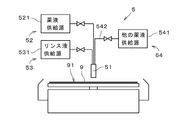
- FIG. 2 is a block diagram showing a processing liquid supply unit 5 of the substrate processing apparatus 1.
- FIG. 2 also shows configurations other than the processing liquid supply unit 5.
- the treatment liquid supply unit 5 includes a chemical liquid supply unit 52 and a rinse liquid supply unit 53.
- the chemical solution supply unit 52 includes a nozzle 51, an arm 511 (see FIG. 1), a nozzle rotation mechanism 512 (see FIG. 1), a chemical solution supply source 521, and a chemical solution pipe 522.
- the nozzle 51 is connected to the chemical solution supply source 521 via the chemical solution pipe 522.
- the nozzle 51 is a chemical liquid discharge unit that discharges the chemical liquid sent from the chemical liquid supply source 521 toward the upper surface 91 of the substrate 9.
- the chemical solution is an etching solution used for wet etching of the substrate 9.
- the etching solution is, for example, an alkaline etching solution such as an aqueous solution of ammonium hydroxide (NH 4 OH).
- the rinse liquid supply unit 53 includes the above-mentioned nozzle 51, an arm 511, a nozzle rotation mechanism 512, a rinse liquid supply source 531 and a rinse liquid pipe 532.
- the nozzle 51 is connected to the rinse liquid supply source 531 via the rinse liquid pipe 532.
- the nozzle 51 is a rinse liquid discharge unit that discharges the rinse liquid delivered from the rinse liquid supply source 531 toward the upper surface 91 of the substrate 9.
- an aqueous treatment liquid such as DIW (De-ionized Water), carbonated water, ozone water or hydrogen water is used.
- the nozzle 51, the arm 511, and the nozzle rotation mechanism 512 are shared by the chemical liquid supply unit 52 and the rinse liquid supply unit 53.
- a discharge port for a chemical liquid and a discharge port for a rinse liquid are individually provided at the lower end of the nozzle 51, and different types of treatment liquids are placed on the upper surface of the substrate 9 via different pipes and discharge ports. It is supplied to 91.
- the nozzle for discharging the chemical solution and the nozzle for discharging the rinse solution may be provided separately.
- the ultraviolet irradiation unit 7 includes an ultraviolet lamp 71 and a lamp elevating mechanism 72.
- the ultraviolet lamp 71 is a substantially disk-shaped lamp arranged above the substrate 9.
- the lamp elevating mechanism 72 is arranged on the outer side in the radial direction of the cup portion 4.
- the lamp elevating mechanism 72 includes, for example, an electric linear motor or a ball screw and an electric rotary motor.
- the lamp elevating mechanism 72 is connected to the ultraviolet lamp 71 and moves the ultraviolet lamp 71 in the vertical direction.
- the ultraviolet lamp 71 can move in the vertical direction between the retracted position shown by the solid line in FIG. 1 and the irradiation position (indicated by the alternate long and short dash line) below the retracted position.
- the nozzle 51 retracts from above the substrate 9 to the retracted position by the nozzle rotation mechanism 512.
- the ultraviolet lamp 71 irradiates ultraviolet rays from the irradiation position toward the entire upper surface 91 of the substrate 9.
- the ultraviolet lamp 71 an excimer lamp, a low-pressure mercury lamp, or the like is used.
- the wavelength of the ultraviolet rays emitted from the ultraviolet lamp 71 is preferably 250 nm or less, more preferably 172 nm or less.
- the lower limit of the wavelength of the ultraviolet rays is not particularly limited, but is, for example, 120 nm or more.
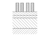
- FIG. 3 is an enlarged cross-sectional view showing a portion of the substrate 9 near the upper surface 91.
- an insulating film 94 is formed on the upper surface of the silicon substrate main body 93
- a titanium nitride (TiN) film 95 is formed on the upper surface of the insulating film 94
- the titanium nitride film 95 is formed.
- a silicon nitride film 96 is formed on the upper surface of the above.
- the insulating film 94, the titanium nitride film 95, and the silicon nitride film 96 are each provided with a substantially uniform thickness on the entire upper surface of the silicon substrate main body 93 in FIG.
- An amorphous silicon layer 97 is formed on the upper surface of the silicon nitride film 96.
- the amorphous silicon layer 97 is a fine pattern that is an aggregate of a plurality of pattern elements 971.
- the amorphous silicon layer 97 is an intermediate pattern formed in the process of multi-patterning with respect to the substrate 9. In FIG. 3, four pattern elements 971 are illustrated.
- the width of the pattern element 971 in FIG. 3 in the left-right direction is, for example, 30 nm to 100 nm.
- the vertical height of the pattern element 971 is, for example, 20 nm to 100 nm.
- the upper surface of the silicon nitride film 96 is exposed between the adjacent pattern elements 971.
- each pattern element 971 of the amorphous silicon layer 97 is covered with a side wall 981.
- the side wall 981 is a thin film formed of a silicon oxide, a silicon nitride, a silicon oxynitride, or the like.
- the width of the side wall 981 in FIG. 3 in the left-right direction is smaller than the width of the pattern element 971, for example, 10 nm to 20 nm.
- the vertical height of the side wall 981 is substantially the same as the height of the pattern element 971, and the upper and lower ends of the side wall 981 are located at substantially the same positions as the upper and lower ends of the pattern element 971 in the vertical direction.
- the upper surface of the pattern element 971 is not covered with the thin film formed of the above-mentioned silicon oxide, silicon nitride, silicon oxynitride or the like, and is exposed from the two side walls 981 covering both side surfaces of the pattern element 971. There is.
- FIG. 4 shows a state in which an insulating film 94, a titanium nitride film 95, a silicon nitride film 96, and an amorphous silicon layer 97 (that is, an intermediate pattern) are formed in this order on the silicon substrate main body 93.
- the coating film 98 covering the uppermost amorphous silicon layer 97 is formed.
- the coating film 98 is, for example, a silicon oxide film, a silicon nitride film, or a silicon oxynitride film.
- the coating film 98 covers the upper surface and side surfaces of each pattern element 971 of the amorphous silicon layer 97, and the upper surface of the silicon nitride film 96 exposed from between the pattern elements 971 over the entire surface.
- the coating film 98 is formed by, for example, CVD (Chemical Vapor Deposition), PVD (Physical Vapor Deposition), or ALD (Atomic Layer Deposition). Will be
- dry etching is performed on the coating film 98 shown in FIG.
- the dry etching is, for example, plasma etching by plasma generated by using a fluorocarbon gas (CxFy) and an oxygen gas.
- the dry etching is anisotropic etching in which etching proceeds substantially only in the vertical direction.
- each pattern element 971 of the amorphous silicon layer 97 is maintained in a state of being covered with the coating film 98.
- the substrate 9 shown in FIG. 3 is formed.
- the side wall 981 covering the side surface of each pattern element 971 is a portion of the above-mentioned coating film 98 (see FIG. 4) left during dry etching.
- oxygen (O) is applied to the upper surface of each pattern element 971 exposed from the coating film 98 (that is, the surface of the amorphous silicon layer 97 opposite to the silicon substrate body 93) during the dry etching.
- Carbon (C), fluorine (F), and the like are incident on the surface, and as shown in FIG. 5, an altered layer 972 is formed on the upper surface of each pattern element 971.
- the altered layer 972 is provided with a parallel diagonal line different from the portion of the pattern element 971 other than the altered layer 972.
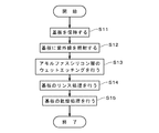
- the substrate 9 having the amorphous silicon layer 97 and the side wall 981 shown in FIG. 3 is carried into the substrate processing apparatus 1 shown in FIG. 1 and held in a horizontal state by the substrate holding portion 31 (step). S11). As shown in FIG. 5, an altered layer 972 derived from dry etching is formed on the surface of the amorphous silicon layer 97.
- the ultraviolet lamp 71 is arranged at the irradiation position indicated by the alternate long and short dash line in FIG. 1, and the ultraviolet lamp 71 to the entire upper surface 91 of the substrate 9 are arranged.
- Ultraviolet rays are emitted toward.
- the altered layer 972 of the amorphous silicon layer 97 is irradiated with ultraviolet rays. Irradiation of ultraviolet rays from the ultraviolet lamp 71 to the altered layer 972 is performed for a predetermined time.
- the Si—O bond and the Si—C bond in the altered layer 972 are cleaved.
- the altered layer 972 is modified to form a modified layer (step S12).
- the wavelength of the ultraviolet rays irradiated to the amorphous silicon layer 97 is preferably 250 nm or less, as described above.
- the energy of ultraviolet rays having a wavelength of 250 nm or less is 478 kJ / mol or more, which is larger than the binding energy of Si—O bond of 443 kJ / mol and the binding energy of Si—C bond of 337 kJ / mol. Therefore, by irradiating the altered layer 972 with ultraviolet rays having a wavelength of 250 nm or less, the Si—O bond and the Si—C bond of the altered layer 972 can be suitably cut.
- the cumulative irradiation amount of ultraviolet rays irradiated from the ultraviolet lamp 71 to the altered layer 972 of the amorphous silicon layer 97 is preferably 1000 mJ / cm 2 or more.
- the upper limit of the integrated irradiation amount is not particularly limited, but is, for example, 3000 mJ / cm 2 .
- the integrated irradiation amount is obtained by integrating the ultraviolet irradiation time (sec) with the ultraviolet illuminance (mW / cm 2 ) on the upper surface of the amorphous silicon layer 97.
- Irradiation of the amorphous silicon layer 97 with ultraviolet rays in step S12 is preferably performed in a low oxygen atmosphere. More preferably, the irradiation of the ultraviolet rays is performed in an atmosphere having an oxygen concentration of 1% by volume or less.
- the low oxygen atmosphere may be realized by various methods. For example, the low oxygen atmosphere is realized by supplying an inert gas such as nitrogen (N 2 ) gas from the airflow forming portion 12 to the internal space of the housing 11 and making the internal space of the housing 11 an inert gas atmosphere. May be done. The supply of the inert gas to the housing 11 may be performed by a gas supply mechanism other than the airflow forming unit 12. Further, the irradiation of the ultraviolet rays may be performed in a low oxygen atmosphere by supplying the inert gas only to the space between the ultraviolet lamp 71 and the substrate 9 from the side of the space or the like.
- N 2 nitrogen
- the ultraviolet lamp 71 is moved from the irradiation position to the retracted position by the lamp elevating mechanism 72. Further, the nozzle rotation mechanism 512 moves the nozzle 51 from the retracted position to the upper side of the substrate 9. Then, the rotation of the substrate 9 by the substrate rotation mechanism 33 is started, and the chemical liquid supply unit 52 is controlled by the supply control unit 63, so that the chemical liquid is supplied from the nozzle 51 to the rotating substrate 9. Specifically, the liquid columnar chemical solution is discharged from the nozzle 51 toward the central portion of the upper surface 91 of the substrate 9. The chemical solution supplied onto the substrate 9 spreads radially outward from the central portion of the substrate 9 by centrifugal force and is applied to the entire upper surface 91 of the substrate 9.
- the chemical solution is an etching solution such as an aqueous ammonium hydroxide solution, and by supplying the chemical solution to the amorphous silicon layer 97 having the modified layer on the surface, wet etching is performed on the amorphous silicon layer 97 (step S13). ..
- etching solution such as an aqueous ammonium hydroxide solution
- the nozzle 51 is reciprocated in the substantially radial direction above the substrate 9 by driving the nozzle rotation mechanism 512 by the supply control unit 63 while the amorphous silicon layer 97 is wet-etched. It may be moved. As a result, the uniformity of applying the etching solution to the entire surface of the substrate 9 can be improved.
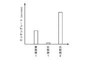
- FIG. 7 is a diagram showing the etching rate of the amorphous silicon layer 97 in the above-mentioned wet etching.
- the etching rate is based on the case where an aqueous solution of ammonium hydroxide at 65 ° C. prepared by mixing ammonium hydroxide and DIW at a ratio of 1:15 is used as the etching solution.
- Example 1 in the figure shows the etching rate of the amorphous silicon layer 97 on which the above-mentioned modified layer is formed on the surface.
- the integrated irradiation amount of ultraviolet rays on the altered layer 972 in step S12 was 1000 mJ / cm 2 .
- Comparative Example 1 shows the etching rate of the amorphous silicon layer 97 (that is, the amorphous silicon layer before ultraviolet irradiation) in which the altered layer 972 is formed on the surface.
- Comparative Example 2 shows the etching rate of the altered layer 972 and the amorphous silicon layer 97 having no modified layer formed on the surface (that is, the amorphous silicon layer not subjected to plasma etching).
- the etching rate of Comparative Example 1 is extremely low, about 3% of the etching rate of Comparative Example 2, because wet etching is inhibited by the altered layer 972. Therefore, in the state of Comparative Example 1, wet etching of the amorphous silicon layer 97 is not substantially performed.
- the etching rate of Example 1 has recovered to about 43% of the etching rate of Comparative Example 2 because the altered layer 972 has been modified by ultraviolet irradiation. Therefore, wet etching of the amorphous silicon layer 97 can be preferably performed.
- the etching rate of Example 1 is 10 times or more the etching rate of Comparative Example 1.
- the substrate processing apparatus 1 by continuing the supply of the chemical solution (that is, the etching solution) from the nozzle 51 for a predetermined time, all the pattern elements 971 of the amorphous silicon layer 97 are removed from between the side walls 981 and the substrate 9 is wetted. Etching is completed.
- the chemical solution that is, the etching solution
- the rinse liquid supply unit 53 is controlled by the supply control unit 63, so that the rinse liquid is supplied from the nozzle 51 to the upper surface 91 of the rotating substrate 9, and the substrate 9 is rinsed. (Step S14). After that, the supply of the rinse liquid is stopped, and the substrate 9 is dried (step S15). In the drying process, the rotation speed of the substrate 9 is increased, and the processing liquid remaining on the substrate 9 is scattered from the edge of the substrate 9 to the outside in the radial direction by centrifugal force and is removed from the substrate 9.
- the treatment liquids such as the chemical liquid and the rinsing liquid scattered radially outward from the substrate 9 during the above steps S13 to S15 are received by the cup portion 4 and discharged to the outside of the housing 11.
- the substrate 9 for which the drying process has been completed is carried out from the substrate processing device 1 and carried into another device for performing a subsequent process.
- the side wall 981 is used as a mask to perform dry etching of the silicon nitride film 96.
- the processes of steps S11 to S15 described above are sequentially performed on the plurality of substrates 9.
- the above-mentioned substrate treatment method includes a step (step S11) of holding the substrate 9 having the amorphous silicon layer 97 in which the alteration layer 972 derived from dry etching is formed on the surface in a horizontal state, and the alteration layer.
- a step (step S13) of performing wet etching on the silicon layer 97 is provided.
- the etching rate of the amorphous silicon layer 97 lowered by the altered layer 972 can be increased.
- wet etching of the amorphous silicon layer 97 can be efficiently performed.
- the coating film 98 formed on the surface of the amorphous silicon layer 97 is etched by the plasma generated by using the fluorocarbon gas and the oxygen gas.
- the Si—O bond and the SiC bond in the altered layer 972 can be cleaved by irradiating the amorphous silicon layer 97 with ultraviolet rays, so that the amorphous silicon layer 97 is reduced by the Si—O bond and the SiC bond.
- the etching rate of the silicon layer 97 can be increased.
- the amorphous silicon layer 97 is an intermediate pattern formed in the process of multi-patterning with respect to the substrate 9. Further, in the above dry etching, anisotropic etching is performed on the coating film 98 covering the upper surface and the side surface of the intermediate pattern, so that the upper surface of the intermediate pattern is exposed from the coating film 98 and covers the side surface of the intermediate pattern. The side wall 981 of the coating film 98 is formed. Then, in the wet etching, the intermediate pattern is removed and the side wall 981 remains. In the substrate processing method, the etching rate of the amorphous silicon layer 97 can be increased by irradiating the altered layer 972 with ultraviolet rays, so that the multi-patterning on the substrate 9 can be efficiently performed.
- the wavelength of the ultraviolet rays irradiated to the altered layer 972 in step S12 is preferably 250 nm or less. Since the energy of ultraviolet rays having a wavelength of 250 nm or less is larger than the binding energy of Si—O bond and the binding energy of Si—C bond, the modification of the altered layer 972 by ultraviolet irradiation (that is, the Si—O bond and Si in the altered layer 972). -C-bond cleavage) can be preferably performed.
- the integrated irradiation amount of ultraviolet rays in step S12 is preferably 1000 mJ / cm 2 or more.
- the alteration layer 972 can be suitably modified by ultraviolet irradiation.
- the irradiation of ultraviolet rays in step S12 is preferably performed in a low oxygen atmosphere. As a result, it is possible to prevent or suppress the absorption of ultraviolet rays in the process of irradiating the amorphous silicon layer 97 by oxygen. As a result, the alteration layer 972 can be efficiently modified by ultraviolet irradiation.
- the above-mentioned substrate processing device 1 includes a substrate holding unit 31, an ultraviolet irradiation unit 7, and a chemical solution supply unit 52.
- the substrate holding portion 31 holds the substrate 9 having the amorphous silicon layer 97 on which the altered layer 972 derived from dry etching is formed on the surface in a horizontal state.
- the ultraviolet irradiation unit 7 modifies the altered layer 972 to form a modified layer by irradiating the altered layer 972 with ultraviolet rays.
- the chemical solution supply unit 52 supplies the chemical solution to the amorphous silicon layer 97 having the modified layer on the surface, and wet-etches the amorphous silicon layer 97.
- the etching rate of the amorphous silicon layer 97 lowered by the altered layer 972 can be increased in the same manner as described above.
- wet etching of the amorphous silicon layer 97 can be efficiently performed.
- step S12 the irradiation of ultraviolet rays on the amorphous silicon layer 97 in step S12 and the supply of a chemical solution (that is, an etching solution) to the amorphous silicon layer 97 in step S13.
- a chemical solution that is, an etching solution
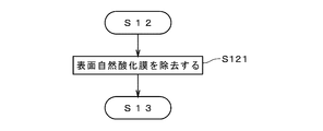
- step S121 the pretreatment for the amorphous silicon layer 97 may be performed.
- step S121 another chemical solution (for example, hydrofluoric acid (HF)) different from the chemical solution of step S13 is supplied to the amorphous silicon layer 97, whereby the surface of the amorphous silicon layer 97 (that is, the altered layer 972) is supplied.
- HF hydrofluoric acid
- the treatment liquid supply unit 5 of the substrate processing apparatus 1 is provided with another chemical liquid that supplies the other chemical liquid to the substrate 9 in addition to the chemical liquid supply unit 52 and the rinse liquid supply unit 53.
- a supply unit 54 is further provided.
- the other chemical solution supply unit 54 includes a nozzle 51, an arm 511 (see FIG. 1), a nozzle rotation mechanism 512 (see FIG. 1), another chemical solution supply source 541, and another chemical solution pipe 542.
- the nozzle 51 is connected to another chemical solution supply source 541 via another chemical solution pipe 542.
- the nozzle 51 is another chemical discharge unit that discharges the other chemicals (for example, dilute hydrofluoric acid at room temperature having a concentration of 0.3%) sent from the other chemical supply source 541 toward the upper surface 91 of the substrate 9. But also.
- the nozzle for discharging the other chemical solution may be provided separately from the nozzle for discharging the etching solution described above.
- the above-mentioned substrate processing method is a step of supplying another chemical solution to the amorphous silicon layer 97 between steps S12 and S13 to remove the surface natural oxide film of the amorphous silicon layer 97 ( It is preferable to further include step S121).
- step S121 By removing the surface natural oxide film before the wet etching of the amorphous silicon layer 97 in this way, it is possible to prevent or suppress a decrease in the etching rate due to the surface natural oxide film. As a result, wet etching of the amorphous silicon layer 97 can be performed more efficiently.
- FIG. 10 is a side view showing the configuration of the substrate processing device 1a.
- the substrate 9 shown in FIG. 3 is subjected to substantially the same processing as that of the substrate processing apparatus 1 shown in FIG. 1, and the amorphous silicon layer 97 is wet-etched.
- the substrate processing device 1a includes an irradiation unit 14, a liquid processing unit 15, a control unit 6, and a housing 11.
- the irradiation unit 14 and the liquid treatment unit 15 are arranged inside one housing 11.
- the control unit 6 has the same structure as the control unit 6 shown in FIG. As described above, the control unit 6 includes a storage unit 61, an irradiation control unit 62, and a supply control unit 63.
- the irradiation unit 14 includes a first substrate holding portion 31a and an ultraviolet irradiation unit 7a.
- the first substrate holding portion 31a has substantially the same structure as the substrate holding portion 31 shown in FIG. 1, and holds the substrate 9 in the horizontal state from below. In the example shown in FIG. 10, the irradiation unit 14 is not provided with the substrate rotation mechanism 33, and the first substrate holding portion 31a does not rotate.
- the ultraviolet irradiation unit 7a includes an ultraviolet lamp 71a and an irradiation area scanning mechanism 73.
- the ultraviolet lamp 71a is a substantially rod-shaped lamp extending substantially linearly in the direction perpendicular to the paper surface in the drawing.
- the ultraviolet rays emitted from the ultraviolet lamp 71a are applied to the band-shaped or linear irradiation region extending substantially linearly in the direction perpendicular to the paper surface on the substrate 9.
- the irradiation region is a part of the upper surface 91 of the substrate 9, and crosses the upper surface 91 of the substrate 9 in a direction perpendicular to the paper surface.
- the ultraviolet lamp 71a an excimer lamp, a low-pressure mercury lamp, or the like is used in the same manner as the above-mentioned ultraviolet lamp 71.
- the wavelength of the ultraviolet rays emitted from the ultraviolet lamp 71a is preferably 250 nm or less, more preferably 172 nm or less.
- the lower limit of the wavelength of the ultraviolet rays is not particularly limited, but is, for example, 120 nm or more.
- the irradiation area scanning mechanism 73 scans the irradiation area on the substrate 9 in the left-right direction in the drawing by moving the ultraviolet lamp 71a above the substrate 9 in the left-right direction in the drawing.
- the irradiation area scanning mechanism 73 includes, for example, an electric linear motor or a ball screw and an electric rotary motor.
- the irradiation control unit 62 of the control unit 6 controls the irradiation region scanning mechanism 73 to control the moving speed of the ultraviolet lamp 71a and control the scanning speed of the ultraviolet irradiation region on the substrate 9. To. While the ultraviolet lamp 71a is moving, the output from the ultraviolet lamp 71a is maintained substantially constant.
- the liquid treatment unit 15 has the same as the substrate processing apparatus 1 shown in FIG. 1, except that the ultraviolet irradiation unit 7 is omitted and the second substrate holding unit 31b having the same structure as the substrate holding unit 31 is provided. It has almost the same structure.
- the same reference numerals are given to the configurations corresponding to the respective configurations of the substrate processing apparatus 1 in the liquid processing unit 15.
- the first substrate holding portion 31a and the second substrate holding portion 31b form a substrate holding portion 31 that holds the substrate 9 in a horizontal state.
- the nozzle rotation mechanism 512 is a discharge position scanning mechanism that scans the discharge position of the chemical liquid on the upper surface 91 of the substrate 9.
- the supply control unit 63 of the control unit 6 controls the nozzle rotation mechanism 512 to control the moving speed of the nozzle 51 and control the scanning speed of the chemical liquid discharge position on the substrate 9.
- the processing flow of the substrate 9 in the substrate processing apparatus 1a is substantially the same as in steps S11 to S15 shown in FIG.
- the substrate 9 having the amorphous silicon layer 97 and the side wall 981 shown in FIG. 3 is carried into the substrate processing apparatus 1a, and is carried by the first substrate holding portion 31a of the irradiation unit 14. It is held in a horizontal state (step S11).
- the altered layer 972 (see FIG. 5) derived from dry etching is formed on the surface of the amorphous silicon layer 97.
- the irradiation control unit 62 controls the ultraviolet irradiation unit 7a of the irradiation unit 14, so that the altered layer 972 of the amorphous silicon layer 97 is irradiated with ultraviolet rays.
- ultraviolet rays are emitted from the ultraviolet lamp 71a and irradiate an irradiation region extending substantially linearly on the upper surface 91 of the substrate 9.
- the irradiation region scanning mechanism 73 scans the ultraviolet lamp 71a above the substrate 9 from the left side to the right side in the drawing, so that the entire upper surface 91 of the substrate 9 is irradiated with ultraviolet rays.
- the Si—O bond and the Si—C bond in the altered layer 972 are cleaved to modify the altered layer 972, and the above-mentioned modified layer is generated (step S12).
- the wavelength of the ultraviolet rays irradiated to the amorphous silicon layer 97 is preferably 250 nm or less as described above.
- the modification of the altered layer 972 by irradiation with ultraviolet rays (that is, the cleavage of the Si—O bond and the Si—C bond in the altered layer 972) can be preferably performed.
- the cumulative irradiation amount of ultraviolet rays irradiated from the ultraviolet lamp 71a to the altered layer 972 of the amorphous silicon layer 97 is preferably 1000 mJ / cm 2 or more as described above. Thereby, the alteration layer 972 can be suitably modified by ultraviolet irradiation.
- Irradiation of the amorphous silicon layer 97 with ultraviolet rays in step S12 is preferably performed in a low oxygen atmosphere. Thereby, similarly to the above, it is possible to prevent or suppress the ultraviolet rays in the process of irradiating the amorphous silicon layer 97 from being absorbed by oxygen. As a result, the alteration layer 972 can be efficiently modified by ultraviolet irradiation.
- the ultraviolet lamp 71a reciprocates in the left-right direction above the substrate 9, so that the substrate 9 may be scanned for ultraviolet rays a plurality of times.
- step S12 the substrate 9 is transported from the irradiation unit 14 to the liquid treatment unit 15 by a transport mechanism (not shown) such as a robot hand, and is held in a horizontal state by the second substrate holding portion 31b of the liquid treatment unit 15. Will be done. Subsequently, the rotation of the substrate 9 by the substrate rotation mechanism 33 is started, and the chemical solution supply unit 52 (see FIG. 2) is controlled by the supply control unit 63, so that the chemical solution (from the nozzle 51) with respect to the rotating substrate 9 (see FIG. 2). That is, the etching solution) is supplied.
- the nozzle 51 is reciprocated in the substantially radial direction above the substrate 9 by the nozzle rotation mechanism 512, and the discharge position of the chemical solution on the upper surface 91 of the substrate 9 is scanned. Then, by supplying the chemical solution to the amorphous silicon layer 97 having the modified layer on the surface, wet etching is performed on the amorphous silicon layer 97 (step S13).
- the rinse liquid is supplied from the nozzle 51 to the upper surface 91 of the rotating substrate 9, and the substrate 9 is rinsed (step S14). After that, the supply of the rinse liquid is stopped, and the substrate 9 is dried (step S15).
- the processes of steps S11 to S15 described above are sequentially performed on the plurality of substrates 9.
- the above-mentioned step S121 may be performed between the steps S12 and S13.
- the etching rate of the amorphous silicon layer 97 lowered by the altered layer 972 can be increased, similarly to the substrate processing apparatus 1 shown in FIG. Specifically, the etching rate of the amorphous silicon layer 97 can be increased by breaking the Si—O bond and the SiC bond in the altered layer 972. As a result, wet etching of the amorphous silicon layer 97 can be efficiently performed. As a result, the multi-patterning on the substrate 9 can be efficiently performed.
- the ultraviolet irradiation region on the substrate 9 is scanned in step S12.
- the scanning speed of the ultraviolet irradiation region with respect to the region of the amorphous silicon layer 97 in which the alteration layer 972 is thick is set to be low in the alteration layer 972. It is made smaller than the scanning speed of the ultraviolet irradiation area with respect to the area.
- the integrated irradiation amount of ultraviolet rays for the region where the altered layer 972 is thick becomes larger than the integrated irradiation amount of ultraviolet rays for the region where the altered layer 972 is thin.
- the uniformity of modification of the altered layer 972 in the entire amorphous silicon layer 97 can be improved.
- the improvement in the uniformity of the modification can be confirmed by the improvement in the uniformity of the etching rate in the entire amorphous silicon layer 97.
- the output of the ultraviolet lamp 71a is controlled by the irradiation control unit 62, and the illuminance of the ultraviolet rays for the region where the alteration layer 972 is thick may be larger than the illuminance of the ultraviolet rays for the region where the alteration layer 972 is thin.
- the integrated irradiation amount of ultraviolet rays for the region where the altered layer 972 is thick and the integrated irradiation amount of ultraviolet rays for the region where the altered layer 972 is thin among the amorphous silicon layers 97. Can be larger than.
- the uniformity of modification of the altered layer 972 in the entire amorphous silicon layer 97 can be improved.
- the discharge position of the chemical solution on the substrate 9 is scanned in step S13.
- the nozzle rotation mechanism 512 that is, the discharge position scanning mechanism
- the supply control unit 63 controls the supply control unit 63, so that the scanning speed of the chemical liquid discharge position with respect to the region where the altered layer 972 is thick in the amorphous silicon layer 97.
- the alteration layer 972 is made smaller than the scanning speed of the ejection position of the chemical solution with respect to the thin region.
- the discharge time of the chemical solution to the region where the altered layer 972 is thick becomes longer than the discharge time of the chemical solution to the region where the altered layer 972 is thin.
- the uniformity of wet etching for example, the uniformity of the progress rate of wet etching
- the irradiation of the amorphous silicon layer 97 with ultraviolet rays in step S12 does not necessarily have to be performed in a low oxygen atmosphere, and may be performed in an air atmosphere, for example.
- the integrated irradiation amount of ultraviolet rays to the amorphous silicon layer 97 may be appropriately changed according to the type and thickness of the altered layer 972.
- the integrated irradiation amount of ultraviolet rays on the amorphous silicon layer 97 may be less than 1000 mJ / cm 2 .
- the wavelength of the ultraviolet rays irradiated to the amorphous silicon layer 97 may be appropriately changed according to the type and thickness of the altered layer 972.
- the wavelength of the ultraviolet rays applied to the amorphous silicon layer 97 may be longer than 250 nm.
- the amorphous silicon layer 97 of the substrate 9 processed in the substrate processing devices 1 and 1a does not necessarily have to be an intermediate pattern formed in the process of multi-patterning with respect to the substrate 9, and the amorphous silicon subjected to processing other than multi-patterning It may be a layer.
- the altered layer 972 modified in the substrate processing apparatus 1, 1a is not necessarily limited to the one formed during plasma etching with plasma generated using fluorocarbon gas and oxygen gas, and other treatments are performed.
- the surface of the amorphous silicon layer 97 may be altered by this.
- the amorphous silicon layer 97 may be irradiated with ultraviolet rays by the ultraviolet irradiation unit 7a shown in FIG. Further, in the substrate processing apparatus 1a, the irradiation of the amorphous silicon layer 97 with ultraviolet rays may be performed by the ultraviolet irradiation unit 7 shown in FIG. Further, in the substrate processing device 1a, the irradiation unit 14 and the liquid processing unit 15 may be housed in different housings.
- the above-mentioned substrate processing device 1 is used for a liquid crystal display device, a glass substrate used for a flat display device (Flat Panel Display) such as an organic EL (Electro Luminescence) display device, or another display device. It may be used for processing a glass substrate to be processed. Further, the above-mentioned substrate processing device 1 may be used for processing an optical disk substrate, a magnetic disk substrate, a magneto-optical disk substrate, a photomask substrate, a ceramic substrate, a solar cell substrate, and the like.
- a flat display device such as an organic EL (Electro Luminescence) display device
- the above-mentioned substrate processing device 1 may be used for processing an optical disk substrate, a magnetic disk substrate, a magneto-optical disk substrate, a photomask substrate, a ceramic substrate, a solar cell substrate, and the like.
Landscapes
- Chemical & Material Sciences (AREA)
- Engineering & Computer Science (AREA)
- Organic Chemistry (AREA)
- Materials Engineering (AREA)
- Mechanical Engineering (AREA)
- Metallurgy (AREA)
- Chemical Kinetics & Catalysis (AREA)
- Inorganic Chemistry (AREA)
- General Chemical & Material Sciences (AREA)
- Weting (AREA)
- Health & Medical Sciences (AREA)
- Toxicology (AREA)
- Physics & Mathematics (AREA)
- Plasma & Fusion (AREA)
Abstract
Description
7,7a 紫外線照射部
9 基板
31 基板保持部
31a 第1基板保持部
31b 第2基板保持部
51 ノズル
52 薬液供給部
54 他の薬液供給部
62 照射制御部
63 供給制御部
71,71a 紫外線ランプ
73 照射領域走査機構
97 アモルファスシリコン層
98 被覆膜
512 ノズル回転機構
972 変質層
981 側壁
S11~S15 ステップ
Claims (18)
- 基板処理方法であって、
a)ドライエッチング由来の変質層が表面に形成されたアモルファスシリコン層を有する基板を水平状態で保持する工程と、
b)前記変質層に紫外線を照射することにより前記変質層を改質して改質層を生成する工程と、
c)前記改質層を表面に有する前記アモルファスシリコン層に薬液を供給して前記アモルファスシリコン層に対するウェットエッチングを行う工程と、
を備える。 - 請求項1に記載の基板処理方法であって、
前記ドライエッチングでは、フルオロカーボン系ガスおよび酸素ガスを用いて生成されたプラズマにより、前記アモルファスシリコン層の表面に形成された被覆膜のエッチングが行われる。 - 請求項2に記載の基板処理方法であって、
前記アモルファスシリコン層は、前記基板に対するマルチパターニング途上で形成された中間パターンであり、
前記ドライエッチングでは、前記中間パターンの上面および側面を覆う前記被覆膜に対する異方性エッチングが行われることにより、前記中間パターンの前記上面が前記被覆膜から露出し、前記中間パターンの前記側面を覆う前記被覆膜の側壁が形成され、
前記ウェットエッチングでは、前記中間パターンが除去されて前記側壁が残る。 - 請求項1ないし3のいずれか1つに記載の基板処理方法であって、
前記紫外線の波長は、250nm以下である。 - 請求項1ないし4のいずれか1つに記載の基板処理方法であって、
前記b)工程における前記紫外線の積算照射量は、1000mJ/cm2以上である。 - 請求項1ないし5のいずれか1つに記載の基板処理方法であって、
前記b)工程における前記紫外線の照射は低酸素雰囲気にて行われる。 - 請求項1ないし6のいずれか1つに記載の基板処理方法であって、
前記b)工程において、前記基板上における前記紫外線の照射領域が走査され、
前記アモルファスシリコン層のうち、前記変質層が厚い領域に対する前記紫外線の積算照射量は、前記変質層が薄い領域に対する前記紫外線の積算照射量よりも大きい。 - 請求項1ないし7のいずれか1つに記載の基板処理方法であって、
前記c)工程において、前記基板上における前記薬液の吐出位置が走査され、
前記アモルファスシリコン層のうち、前記改質層が厚い領域に対する前記薬液の吐出時間は、前記改質層が薄い領域に対する前記薬液の吐出時間よりも長い。 - 請求項1ないし8のいずれか1つに記載の基板処理方法であって、
前記b)工程と前記c)工程との間に、前記アモルファスシリコン層に他の薬液を供給して前記アモルファスシリコン層の表面自然酸化膜を除去する工程をさらに備える。 - 基板処理装置であって、
ドライエッチング由来の変質層が表面に形成されたアモルファスシリコン層を有する基板を水平状態で保持する基板保持部と、
前記変質層に紫外線を照射することにより前記変質層を改質して改質層を生成する紫外線照射部と、
前記改質層を表面に有する前記アモルファスシリコン層に薬液を供給して前記アモルファスシリコン層に対するウェットエッチングを行う薬液供給部と、
を備える。 - 請求項10に記載の基板処理装置であって、
前記ドライエッチングでは、フルオロカーボン系ガスおよび酸素ガスを用いて生成されたプラズマにより、前記アモルファスシリコン層の表面に形成された被覆膜のエッチングが行われる。 - 請求項11に記載の基板処理装置であって、
前記アモルファスシリコン層は、前記基板に対するマルチパターニング途上で形成された中間パターンであり、
前記ドライエッチングでは、前記中間パターンの上面および側面を覆う前記被覆膜に対する異方性エッチングが行われることにより、前記中間パターンの前記上面が前記被覆膜から露出し、前記中間パターンの前記側面を覆う前記被覆膜の側壁が形成され、
前記ウェットエッチングでは、前記中間パターンが除去されて前記側壁が残る。 - 請求項10ないし12のいずれか1つに記載の基板処理装置であって、
前記紫外線の波長は、250nm以下である。 - 請求項10ないし13のいずれか1つに記載の基板処理装置であって、
前記アモルファスシリコン層に対する前記紫外線の積算照射量は、1000mJ/cm2以上である。 - 請求項10ないし14のいずれか1つに記載の基板処理装置であって、
前記アモルファスシリコン層に対する前記紫外線の照射は低酸素雰囲気にて行われる。 - 請求項10ないし15のいずれか1つに記載の基板処理装置であって、
前記紫外線照射部を制御する照射制御部をさらに備え、
前記紫外線照射部は、
前記基板に前記紫外線を照射する紫外線ランプと、
前記基板上における前記紫外線の照射領域を走査する照射領域走査機構と、
を備え、
前記照射制御部が前記紫外線ランプおよび前記照射領域走査機構の少なくとも一方を制御することにより、前記アモルファスシリコン層のうち、前記変質層が厚い領域に対する前記紫外線の積算照射量が、前記変質層が薄い領域に対する前記紫外線の積算照射量よりも大きくされる。 - 請求項10ないし16のいずれか1つに記載の基板処理装置であって、
前記薬液供給部を制御する供給制御部をさらに備え、
前記薬液供給部は、
前記基板に前記薬液を吐出する薬液吐出部と、
前記基板上における前記薬液の吐出位置を走査する吐出位置走査機構と、
を備え、
前記供給制御部が前記吐出位置走査機構を制御することにより、前記アモルファスシリコン層のうち、前記改質層が厚い領域に対する前記薬液の吐出時間が、前記改質層が薄い領域に対する前記薬液の吐出時間よりも長くされる。 - 請求項10ないし17のいずれか1つに記載の基板処理装置であって、
前記アモルファスシリコン層に対する前記紫外線の照射と前記薬液の供給との間において、前記アモルファスシリコン層に他の薬液を供給して前記アモルファスシリコン層の表面自然酸化膜を除去する他の薬液供給部をさらに備える。
Priority Applications (4)
| Application Number | Priority Date | Filing Date | Title |
|---|---|---|---|
| KR1020217032957A KR102714578B1 (ko) | 2019-03-20 | 2020-01-08 | 기판 처리 방법 및 기판 처리 장치 |
| CN202080022833.1A CN113614889B (zh) | 2019-03-20 | 2020-01-08 | 衬底处理方法及衬底处理装置 |
| US17/439,445 US11881403B2 (en) | 2019-03-20 | 2020-01-08 | Substrate processing method and substrate processing apparatus |
| CN202510632444.5A CN120497130A (zh) | 2019-03-20 | 2020-01-08 | 衬底处理方法及衬底处理装置 |
Applications Claiming Priority (2)
| Application Number | Priority Date | Filing Date | Title |
|---|---|---|---|
| JP2019-053164 | 2019-03-20 | ||
| JP2019053164A JP7126468B2 (ja) | 2019-03-20 | 2019-03-20 | 基板処理方法および基板処理装置 |
Publications (1)
| Publication Number | Publication Date |
|---|---|
| WO2020188958A1 true WO2020188958A1 (ja) | 2020-09-24 |
Family
ID=72519061
Family Applications (1)
| Application Number | Title | Priority Date | Filing Date |
|---|---|---|---|
| PCT/JP2020/000321 Ceased WO2020188958A1 (ja) | 2019-03-20 | 2020-01-08 | 基板処理方法および基板処理装置 |
Country Status (6)
| Country | Link |
|---|---|
| US (1) | US11881403B2 (ja) |
| JP (1) | JP7126468B2 (ja) |
| KR (1) | KR102714578B1 (ja) |
| CN (2) | CN120497130A (ja) |
| TW (1) | TWI753353B (ja) |
| WO (1) | WO2020188958A1 (ja) |
Families Citing this family (3)
| Publication number | Priority date | Publication date | Assignee | Title |
|---|---|---|---|---|
| US12266533B2 (en) * | 2021-06-01 | 2025-04-01 | Tokyo Electron Limited | Sacrificial capping layer for contact etch |
| CN115831716A (zh) * | 2022-12-27 | 2023-03-21 | 广东芯粤能半导体有限公司 | 碳化硅衬底的回收方法及回收系统 |
| KR102614406B1 (ko) | 2023-08-10 | 2023-12-15 | 주식회사 엠텍마이크라텍글로벌 | Led 광원을 이용한 웨이퍼 엣지 노광 장치 |
Citations (6)
| Publication number | Priority date | Publication date | Assignee | Title |
|---|---|---|---|---|
| JPH04180624A (ja) * | 1990-11-15 | 1992-06-26 | Nec Corp | パターンの形成方法 |
| JPH07283198A (ja) * | 1994-04-05 | 1995-10-27 | Sony Corp | 半導体装置の製造方法 |
| JPH0878352A (ja) * | 1994-09-06 | 1996-03-22 | Sanyo Electric Co Ltd | 基板の処理方法 |
| JP2001085387A (ja) * | 1999-09-13 | 2001-03-30 | Toshiba Corp | 半導体装置の製造方法 |
| JP2002093740A (ja) * | 2000-09-13 | 2002-03-29 | Seiko Epson Corp | 半導体装置の製造方法 |
| JP2011192764A (ja) * | 2010-03-15 | 2011-09-29 | Fujitsu Semiconductor Ltd | 膜の除去方法及び膜除去用装置 |
Family Cites Families (14)
| Publication number | Priority date | Publication date | Assignee | Title |
|---|---|---|---|---|
| JPH0653186A (ja) * | 1992-07-29 | 1994-02-25 | Sony Corp | ドライエッチング方法 |
| JPH0817815A (ja) * | 1994-06-30 | 1996-01-19 | Toshiba Corp | 半導体デバイスの製造方法、半導体基板の処理方法、分析方法及び製造方法 |
| US20040038438A1 (en) | 2002-08-23 | 2004-02-26 | Toppoly Optoelectronics Corp. | Method for reducing surface roughness of polysilicon films for liquid crystal displays |
| JP3776092B2 (ja) * | 2003-03-25 | 2006-05-17 | 株式会社ルネサステクノロジ | エッチング装置、エッチング方法および半導体装置の製造方法 |
| JP4661753B2 (ja) | 2006-09-29 | 2011-03-30 | 東京エレクトロン株式会社 | 基板処理方法、洗浄方法及び記憶媒体 |
| JP2013110139A (ja) | 2011-11-17 | 2013-06-06 | Tokyo Electron Ltd | 半導体装置の製造方法 |
| US9059001B2 (en) * | 2011-12-16 | 2015-06-16 | Taiwan Semiconductor Manufacturing Company, Ltd. | Semiconductor device with biased feature |
| JP6435385B2 (ja) | 2012-05-15 | 2018-12-05 | 株式会社Screenホールディングス | 基板処理用の薬液生成方法、基板処理用の薬液生成ユニット、基板処理方法、および基板処理システム |
| JP6300139B2 (ja) | 2012-05-15 | 2018-03-28 | 株式会社Screenホールディングス | 基板処理方法および基板処理システム |
| JP2014044987A (ja) | 2012-08-24 | 2014-03-13 | Fujitsu Semiconductor Ltd | ダイシング方法及びダイシング装置 |
| TWI697593B (zh) * | 2014-10-31 | 2020-07-01 | 美商維克儀器公司 | 用於執行濕蝕刻製程的系統及方法 |
| WO2018198288A1 (ja) * | 2017-04-27 | 2018-11-01 | 株式会社島津製作所 | ポンプ監視装置、真空処理装置および真空ポンプ |
| US9991129B1 (en) * | 2017-05-23 | 2018-06-05 | Applied Materials, Inc. | Selective etching of amorphous silicon over epitaxial silicon |
| JP6807278B2 (ja) | 2017-05-24 | 2021-01-06 | 東京エレクトロン株式会社 | シリコン窒化膜の成膜方法および成膜装置 |
-
2019
- 2019-03-20 JP JP2019053164A patent/JP7126468B2/ja active Active
-
2020
- 2020-01-08 WO PCT/JP2020/000321 patent/WO2020188958A1/ja not_active Ceased
- 2020-01-08 CN CN202510632444.5A patent/CN120497130A/zh active Pending
- 2020-01-08 KR KR1020217032957A patent/KR102714578B1/ko active Active
- 2020-01-08 CN CN202080022833.1A patent/CN113614889B/zh active Active
- 2020-01-08 US US17/439,445 patent/US11881403B2/en active Active
- 2020-01-15 TW TW109101340A patent/TWI753353B/zh active
Patent Citations (6)
| Publication number | Priority date | Publication date | Assignee | Title |
|---|---|---|---|---|
| JPH04180624A (ja) * | 1990-11-15 | 1992-06-26 | Nec Corp | パターンの形成方法 |
| JPH07283198A (ja) * | 1994-04-05 | 1995-10-27 | Sony Corp | 半導体装置の製造方法 |
| JPH0878352A (ja) * | 1994-09-06 | 1996-03-22 | Sanyo Electric Co Ltd | 基板の処理方法 |
| JP2001085387A (ja) * | 1999-09-13 | 2001-03-30 | Toshiba Corp | 半導体装置の製造方法 |
| JP2002093740A (ja) * | 2000-09-13 | 2002-03-29 | Seiko Epson Corp | 半導体装置の製造方法 |
| JP2011192764A (ja) * | 2010-03-15 | 2011-09-29 | Fujitsu Semiconductor Ltd | 膜の除去方法及び膜除去用装置 |
Also Published As
| Publication number | Publication date |
|---|---|
| TW202036674A (zh) | 2020-10-01 |
| US11881403B2 (en) | 2024-01-23 |
| KR102714578B1 (ko) | 2024-10-11 |
| CN113614889A (zh) | 2021-11-05 |
| CN120497130A (zh) | 2025-08-15 |
| JP2020155603A (ja) | 2020-09-24 |
| CN113614889B (zh) | 2025-06-06 |
| US20220189773A1 (en) | 2022-06-16 |
| TWI753353B (zh) | 2022-01-21 |
| KR20210137178A (ko) | 2021-11-17 |
| JP7126468B2 (ja) | 2022-08-26 |
Similar Documents
| Publication | Publication Date | Title |
|---|---|---|
| CN103367111B (zh) | 基板处理方法以及基板处理装置 | |
| TWI698906B (zh) | 基板處理方法以及基板處理裝置 | |
| KR102166974B1 (ko) | 에칭 후 폴리머의 제거 및 하드마스크 제거의 향상을 위한 방법 및 하드웨어 | |
| CN100517602C (zh) | 基板的处理方法、电子器件的制造方法和程序 | |
| CN102881617B (zh) | 基板处理方法及基板处理装置 | |
| KR20010038404A (ko) | 산화막 제거방법 및 산화막 제거를 위한 반도체 제조 장치 | |
| JP6826890B2 (ja) | 基板処理方法および基板処理装置 | |
| WO2015064546A1 (ja) | 犠牲膜除去方法および基板処理装置 | |
| WO2017047625A1 (ja) | 基板処理方法、基板処理装置および記憶媒体 | |
| CN113614889B (zh) | 衬底处理方法及衬底处理装置 | |
| US11145516B2 (en) | Substrate processing method and substrate processing apparatus | |
| JP4236109B2 (ja) | 基板処理方法及び基板処理装置 | |
| TWI720387B (zh) | 基板處理裝置及基板處理方法 | |
| JP2020184624A (ja) | 膜質除去方法、基板処理方法、及び基板処理装置 | |
| JP4299638B2 (ja) | 基板処理装置および基板処理方法 | |
| JP7182880B2 (ja) | 基板処理方法および基板処理装置 | |
| JP7667167B2 (ja) | コア除去 | |
| TWI828373B (zh) | 基板處理方法及基板處理裝置 | |
| TW202301424A (zh) | 基板處理方法及基板處理裝置 | |
| JP2005353978A (ja) | シリル化処理装置およびシリル化処理方法 | |
| WO2019198575A1 (ja) | 基板処理方法および基板処理装置 | |
| JP2006351805A (ja) | 基板処理方法および基板処理装置 | |
| JP2006054378A (ja) | 基板処理方法および基板処理装置 |
Legal Events
| Date | Code | Title | Description |
|---|---|---|---|
| 121 | Ep: the epo has been informed by wipo that ep was designated in this application |
Ref document number: 20773563 Country of ref document: EP Kind code of ref document: A1 |
|
| NENP | Non-entry into the national phase |
Ref country code: DE |
|
| ENP | Entry into the national phase |
Ref document number: 20217032957 Country of ref document: KR Kind code of ref document: A |
|
| 122 | Ep: pct application non-entry in european phase |
Ref document number: 20773563 Country of ref document: EP Kind code of ref document: A1 |
|
| WWG | Wipo information: grant in national office |
Ref document number: 202080022833.1 Country of ref document: CN |