WO2020179875A1 - 電子部品装置を製造する方法、及びこれに用いられる積層フィルム - Google Patents
電子部品装置を製造する方法、及びこれに用いられる積層フィルム Download PDFInfo
- Publication number
- WO2020179875A1 WO2020179875A1 PCT/JP2020/009476 JP2020009476W WO2020179875A1 WO 2020179875 A1 WO2020179875 A1 WO 2020179875A1 JP 2020009476 W JP2020009476 W JP 2020009476W WO 2020179875 A1 WO2020179875 A1 WO 2020179875A1
- Authority
- WO
- WIPO (PCT)
- Prior art keywords
- adhesive layer
- layer
- sealing
- rewiring
- electronic component
- Prior art date
- Legal status (The legal status is an assumption and is not a legal conclusion. Google has not performed a legal analysis and makes no representation as to the accuracy of the status listed.)
- Ceased
Links
Images




Classifications
-
- H—ELECTRICITY
- H10—SEMICONDUCTOR DEVICES; ELECTRIC SOLID-STATE DEVICES NOT OTHERWISE PROVIDED FOR
- H10W—GENERIC PACKAGES, INTERCONNECTIONS, CONNECTORS OR OTHER CONSTRUCTIONAL DETAILS OF DEVICES COVERED BY CLASS H10
- H10W70/00—Package substrates; Interposers; Redistribution layers [RDL]
- H10W70/01—Manufacture or treatment
- H10W70/05—Manufacture or treatment of insulating or insulated package substrates, or of interposers, or of redistribution layers
- H10W70/08—Manufacture or treatment of insulating or insulated package substrates, or of interposers, or of redistribution layers by depositing layers on the chip or wafer, e.g. "chip-first" RDLs
- H10W70/09—Manufacture or treatment of insulating or insulated package substrates, or of interposers, or of redistribution layers by depositing layers on the chip or wafer, e.g. "chip-first" RDLs extending onto an encapsulation that laterally surrounds the chip or wafer, e.g. fan-out wafer level package [FOWLP] RDLs
-
- H—ELECTRICITY
- H10—SEMICONDUCTOR DEVICES; ELECTRIC SOLID-STATE DEVICES NOT OTHERWISE PROVIDED FOR
- H10W—GENERIC PACKAGES, INTERCONNECTIONS, CONNECTORS OR OTHER CONSTRUCTIONAL DETAILS OF DEVICES COVERED BY CLASS H10
- H10W42/00—Arrangements for protection of devices
- H10W42/20—Arrangements for protection of devices protecting against electromagnetic or particle radiation, e.g. light, X-rays, gamma-rays or electrons
-
- H—ELECTRICITY
- H10—SEMICONDUCTOR DEVICES; ELECTRIC SOLID-STATE DEVICES NOT OTHERWISE PROVIDED FOR
- H10W—GENERIC PACKAGES, INTERCONNECTIONS, CONNECTORS OR OTHER CONSTRUCTIONAL DETAILS OF DEVICES COVERED BY CLASS H10
- H10W42/00—Arrangements for protection of devices
- H10W42/20—Arrangements for protection of devices protecting against electromagnetic or particle radiation, e.g. light, X-rays, gamma-rays or electrons
- H10W42/261—Arrangements for protection of devices protecting against electromagnetic or particle radiation, e.g. light, X-rays, gamma-rays or electrons characterised by their shapes or dispositions
- H10W42/276—Arrangements for protection of devices protecting against electromagnetic or particle radiation, e.g. light, X-rays, gamma-rays or electrons characterised by their shapes or dispositions the arrangements being on an external surface of the package, e.g. on the outer surface of an encapsulation
-
- H—ELECTRICITY
- H10—SEMICONDUCTOR DEVICES; ELECTRIC SOLID-STATE DEVICES NOT OTHERWISE PROVIDED FOR
- H10W—GENERIC PACKAGES, INTERCONNECTIONS, CONNECTORS OR OTHER CONSTRUCTIONAL DETAILS OF DEVICES COVERED BY CLASS H10
- H10W46/00—Marks applied to devices, e.g. for alignment or identification
-
- H—ELECTRICITY
- H10—SEMICONDUCTOR DEVICES; ELECTRIC SOLID-STATE DEVICES NOT OTHERWISE PROVIDED FOR
- H10W—GENERIC PACKAGES, INTERCONNECTIONS, CONNECTORS OR OTHER CONSTRUCTIONAL DETAILS OF DEVICES COVERED BY CLASS H10
- H10W70/00—Package substrates; Interposers; Redistribution layers [RDL]
- H10W70/01—Manufacture or treatment
- H10W70/05—Manufacture or treatment of insulating or insulated package substrates, or of interposers, or of redistribution layers
-
- H—ELECTRICITY
- H10—SEMICONDUCTOR DEVICES; ELECTRIC SOLID-STATE DEVICES NOT OTHERWISE PROVIDED FOR
- H10W—GENERIC PACKAGES, INTERCONNECTIONS, CONNECTORS OR OTHER CONSTRUCTIONAL DETAILS OF DEVICES COVERED BY CLASS H10
- H10W70/00—Package substrates; Interposers; Redistribution layers [RDL]
- H10W70/01—Manufacture or treatment
- H10W70/05—Manufacture or treatment of insulating or insulated package substrates, or of interposers, or of redistribution layers
- H10W70/093—Connecting or disconnecting other interconnections thereto or therefrom, e.g. connecting bond wires or bumps
-
- H—ELECTRICITY
- H10—SEMICONDUCTOR DEVICES; ELECTRIC SOLID-STATE DEVICES NOT OTHERWISE PROVIDED FOR
- H10W—GENERIC PACKAGES, INTERCONNECTIONS, CONNECTORS OR OTHER CONSTRUCTIONAL DETAILS OF DEVICES COVERED BY CLASS H10
- H10W70/00—Package substrates; Interposers; Redistribution layers [RDL]
- H10W70/60—Insulating or insulated package substrates; Interposers; Redistribution layers
- H10W70/611—Insulating or insulated package substrates; Interposers; Redistribution layers for connecting multiple chips together
-
- H—ELECTRICITY
- H10—SEMICONDUCTOR DEVICES; ELECTRIC SOLID-STATE DEVICES NOT OTHERWISE PROVIDED FOR
- H10W—GENERIC PACKAGES, INTERCONNECTIONS, CONNECTORS OR OTHER CONSTRUCTIONAL DETAILS OF DEVICES COVERED BY CLASS H10
- H10W70/00—Package substrates; Interposers; Redistribution layers [RDL]
- H10W70/60—Insulating or insulated package substrates; Interposers; Redistribution layers
- H10W70/611—Insulating or insulated package substrates; Interposers; Redistribution layers for connecting multiple chips together
- H10W70/614—Insulating or insulated package substrates; Interposers; Redistribution layers for connecting multiple chips together the multiple chips being integrally enclosed
-
- H—ELECTRICITY
- H10—SEMICONDUCTOR DEVICES; ELECTRIC SOLID-STATE DEVICES NOT OTHERWISE PROVIDED FOR
- H10W—GENERIC PACKAGES, INTERCONNECTIONS, CONNECTORS OR OTHER CONSTRUCTIONAL DETAILS OF DEVICES COVERED BY CLASS H10
- H10W70/00—Package substrates; Interposers; Redistribution layers [RDL]
- H10W70/60—Insulating or insulated package substrates; Interposers; Redistribution layers
- H10W70/62—Insulating or insulated package substrates; Interposers; Redistribution layers characterised by their interconnections
- H10W70/65—Shapes or dispositions of interconnections
-
- H—ELECTRICITY
- H10—SEMICONDUCTOR DEVICES; ELECTRIC SOLID-STATE DEVICES NOT OTHERWISE PROVIDED FOR
- H10W—GENERIC PACKAGES, INTERCONNECTIONS, CONNECTORS OR OTHER CONSTRUCTIONAL DETAILS OF DEVICES COVERED BY CLASS H10
- H10W70/00—Package substrates; Interposers; Redistribution layers [RDL]
- H10W70/60—Insulating or insulated package substrates; Interposers; Redistribution layers
- H10W70/67—Insulating or insulated package substrates; Interposers; Redistribution layers characterised by their insulating layers or insulating parts
- H10W70/68—Shapes or dispositions thereof
- H10W70/685—Shapes or dispositions thereof comprising multiple insulating layers
-
- H—ELECTRICITY
- H10—SEMICONDUCTOR DEVICES; ELECTRIC SOLID-STATE DEVICES NOT OTHERWISE PROVIDED FOR
- H10W—GENERIC PACKAGES, INTERCONNECTIONS, CONNECTORS OR OTHER CONSTRUCTIONAL DETAILS OF DEVICES COVERED BY CLASS H10
- H10W74/00—Encapsulations, e.g. protective coatings
- H10W74/01—Manufacture or treatment
- H10W74/016—Manufacture or treatment using moulds
-
- H—ELECTRICITY
- H10—SEMICONDUCTOR DEVICES; ELECTRIC SOLID-STATE DEVICES NOT OTHERWISE PROVIDED FOR
- H10W—GENERIC PACKAGES, INTERCONNECTIONS, CONNECTORS OR OTHER CONSTRUCTIONAL DETAILS OF DEVICES COVERED BY CLASS H10
- H10W74/00—Encapsulations, e.g. protective coatings
- H10W74/01—Manufacture or treatment
- H10W74/019—Manufacture or treatment using temporary auxiliary substrates
-
- H—ELECTRICITY
- H10—SEMICONDUCTOR DEVICES; ELECTRIC SOLID-STATE DEVICES NOT OTHERWISE PROVIDED FOR
- H10W—GENERIC PACKAGES, INTERCONNECTIONS, CONNECTORS OR OTHER CONSTRUCTIONAL DETAILS OF DEVICES COVERED BY CLASS H10
- H10W74/00—Encapsulations, e.g. protective coatings
- H10W74/10—Encapsulations, e.g. protective coatings characterised by their shape or disposition
- H10W74/111—Encapsulations, e.g. protective coatings characterised by their shape or disposition the semiconductor body being completely enclosed
- H10W74/114—Encapsulations, e.g. protective coatings characterised by their shape or disposition the semiconductor body being completely enclosed by a substrate and the encapsulations
- H10W74/117—Encapsulations, e.g. protective coatings characterised by their shape or disposition the semiconductor body being completely enclosed by a substrate and the encapsulations the substrate having spherical bumps for external connection
-
- H—ELECTRICITY
- H10—SEMICONDUCTOR DEVICES; ELECTRIC SOLID-STATE DEVICES NOT OTHERWISE PROVIDED FOR
- H10W—GENERIC PACKAGES, INTERCONNECTIONS, CONNECTORS OR OTHER CONSTRUCTIONAL DETAILS OF DEVICES COVERED BY CLASS H10
- H10W90/00—Package configurations
-
- H—ELECTRICITY
- H10—SEMICONDUCTOR DEVICES; ELECTRIC SOLID-STATE DEVICES NOT OTHERWISE PROVIDED FOR
- H10P—GENERIC PROCESSES OR APPARATUS FOR THE MANUFACTURE OR TREATMENT OF DEVICES COVERED BY CLASS H10
- H10P72/00—Handling or holding of wafers, substrates or devices during manufacture or treatment thereof
- H10P72/70—Handling or holding of wafers, substrates or devices during manufacture or treatment thereof for supporting or gripping
- H10P72/74—Handling or holding of wafers, substrates or devices during manufacture or treatment thereof for supporting or gripping using temporarily an auxiliary support
- H10P72/7428—Handling or holding of wafers, substrates or devices during manufacture or treatment thereof for supporting or gripping using temporarily an auxiliary support used to support diced chips prior to mounting
-
- H—ELECTRICITY
- H10—SEMICONDUCTOR DEVICES; ELECTRIC SOLID-STATE DEVICES NOT OTHERWISE PROVIDED FOR
- H10P—GENERIC PROCESSES OR APPARATUS FOR THE MANUFACTURE OR TREATMENT OF DEVICES COVERED BY CLASS H10
- H10P72/00—Handling or holding of wafers, substrates or devices during manufacture or treatment thereof
- H10P72/70—Handling or holding of wafers, substrates or devices during manufacture or treatment thereof for supporting or gripping
- H10P72/74—Handling or holding of wafers, substrates or devices during manufacture or treatment thereof for supporting or gripping using temporarily an auxiliary support
- H10P72/743—Handling or holding of wafers, substrates or devices during manufacture or treatment thereof for supporting or gripping using temporarily an auxiliary support used as a support during manufacture of interconnect decals or build up layers
-
- H—ELECTRICITY
- H10—SEMICONDUCTOR DEVICES; ELECTRIC SOLID-STATE DEVICES NOT OTHERWISE PROVIDED FOR
- H10P—GENERIC PROCESSES OR APPARATUS FOR THE MANUFACTURE OR TREATMENT OF DEVICES COVERED BY CLASS H10
- H10P72/00—Handling or holding of wafers, substrates or devices during manufacture or treatment thereof
- H10P72/70—Handling or holding of wafers, substrates or devices during manufacture or treatment thereof for supporting or gripping
- H10P72/74—Handling or holding of wafers, substrates or devices during manufacture or treatment thereof for supporting or gripping using temporarily an auxiliary support
- H10P72/744—Details of chemical or physical process used for separating the auxiliary support from a device or a wafer
-
- H—ELECTRICITY
- H10—SEMICONDUCTOR DEVICES; ELECTRIC SOLID-STATE DEVICES NOT OTHERWISE PROVIDED FOR
- H10P—GENERIC PROCESSES OR APPARATUS FOR THE MANUFACTURE OR TREATMENT OF DEVICES COVERED BY CLASS H10
- H10P72/00—Handling or holding of wafers, substrates or devices during manufacture or treatment thereof
- H10P72/70—Handling or holding of wafers, substrates or devices during manufacture or treatment thereof for supporting or gripping
- H10P72/74—Handling or holding of wafers, substrates or devices during manufacture or treatment thereof for supporting or gripping using temporarily an auxiliary support
- H10P72/744—Details of chemical or physical process used for separating the auxiliary support from a device or a wafer
- H10P72/7442—Separation by peeling
-
- H—ELECTRICITY
- H10—SEMICONDUCTOR DEVICES; ELECTRIC SOLID-STATE DEVICES NOT OTHERWISE PROVIDED FOR
- H10W—GENERIC PACKAGES, INTERCONNECTIONS, CONNECTORS OR OTHER CONSTRUCTIONAL DETAILS OF DEVICES COVERED BY CLASS H10
- H10W46/00—Marks applied to devices, e.g. for alignment or identification
- H10W46/301—Marks applied to devices, e.g. for alignment or identification for alignment
-
- H—ELECTRICITY
- H10—SEMICONDUCTOR DEVICES; ELECTRIC SOLID-STATE DEVICES NOT OTHERWISE PROVIDED FOR
- H10W—GENERIC PACKAGES, INTERCONNECTIONS, CONNECTORS OR OTHER CONSTRUCTIONAL DETAILS OF DEVICES COVERED BY CLASS H10
- H10W46/00—Marks applied to devices, e.g. for alignment or identification
- H10W46/601—Marks applied to devices, e.g. for alignment or identification for use after dicing
- H10W46/607—Located on parts of packages, e.g. on encapsulations or on package substrates
-
- H—ELECTRICITY
- H10—SEMICONDUCTOR DEVICES; ELECTRIC SOLID-STATE DEVICES NOT OTHERWISE PROVIDED FOR
- H10W—GENERIC PACKAGES, INTERCONNECTIONS, CONNECTORS OR OTHER CONSTRUCTIONAL DETAILS OF DEVICES COVERED BY CLASS H10
- H10W70/00—Package substrates; Interposers; Redistribution layers [RDL]
- H10W70/60—Insulating or insulated package substrates; Interposers; Redistribution layers
- H10W70/62—Insulating or insulated package substrates; Interposers; Redistribution layers characterised by their interconnections
- H10W70/63—Vias, e.g. via plugs
-
- H—ELECTRICITY
- H10—SEMICONDUCTOR DEVICES; ELECTRIC SOLID-STATE DEVICES NOT OTHERWISE PROVIDED FOR
- H10W—GENERIC PACKAGES, INTERCONNECTIONS, CONNECTORS OR OTHER CONSTRUCTIONAL DETAILS OF DEVICES COVERED BY CLASS H10
- H10W70/00—Package substrates; Interposers; Redistribution layers [RDL]
- H10W70/60—Insulating or insulated package substrates; Interposers; Redistribution layers
- H10W70/62—Insulating or insulated package substrates; Interposers; Redistribution layers characterised by their interconnections
- H10W70/65—Shapes or dispositions of interconnections
- H10W70/652—Cross-sectional shapes
- H10W70/6523—Cross-sectional shapes for connecting to pads at different heights at the same side of the package substrate, interposer or RDL
-
- H—ELECTRICITY
- H10—SEMICONDUCTOR DEVICES; ELECTRIC SOLID-STATE DEVICES NOT OTHERWISE PROVIDED FOR
- H10W—GENERIC PACKAGES, INTERCONNECTIONS, CONNECTORS OR OTHER CONSTRUCTIONAL DETAILS OF DEVICES COVERED BY CLASS H10
- H10W70/00—Package substrates; Interposers; Redistribution layers [RDL]
- H10W70/60—Insulating or insulated package substrates; Interposers; Redistribution layers
- H10W70/62—Insulating or insulated package substrates; Interposers; Redistribution layers characterised by their interconnections
- H10W70/65—Shapes or dispositions of interconnections
- H10W70/652—Cross-sectional shapes
- H10W70/6528—Cross-sectional shapes of the portions that connect to chips, wafers or package parts
-
- H—ELECTRICITY
- H10—SEMICONDUCTOR DEVICES; ELECTRIC SOLID-STATE DEVICES NOT OTHERWISE PROVIDED FOR
- H10W—GENERIC PACKAGES, INTERCONNECTIONS, CONNECTORS OR OTHER CONSTRUCTIONAL DETAILS OF DEVICES COVERED BY CLASS H10
- H10W72/00—Interconnections or connectors in packages
- H10W72/01—Manufacture or treatment
- H10W72/0198—Manufacture or treatment batch processes
-
- H—ELECTRICITY
- H10—SEMICONDUCTOR DEVICES; ELECTRIC SOLID-STATE DEVICES NOT OTHERWISE PROVIDED FOR
- H10W—GENERIC PACKAGES, INTERCONNECTIONS, CONNECTORS OR OTHER CONSTRUCTIONAL DETAILS OF DEVICES COVERED BY CLASS H10
- H10W72/00—Interconnections or connectors in packages
- H10W72/071—Connecting or disconnecting
- H10W72/072—Connecting or disconnecting of bump connectors
-
- H—ELECTRICITY
- H10—SEMICONDUCTOR DEVICES; ELECTRIC SOLID-STATE DEVICES NOT OTHERWISE PROVIDED FOR
- H10W—GENERIC PACKAGES, INTERCONNECTIONS, CONNECTORS OR OTHER CONSTRUCTIONAL DETAILS OF DEVICES COVERED BY CLASS H10
- H10W72/00—Interconnections or connectors in packages
- H10W72/071—Connecting or disconnecting
- H10W72/072—Connecting or disconnecting of bump connectors
- H10W72/07202—Connecting or disconnecting of bump connectors using auxiliary members
- H10W72/07204—Connecting or disconnecting of bump connectors using auxiliary members using temporary auxiliary members, e.g. sacrificial coatings
- H10W72/07207—Temporary substrates, e.g. removable substrates
-
- H—ELECTRICITY
- H10—SEMICONDUCTOR DEVICES; ELECTRIC SOLID-STATE DEVICES NOT OTHERWISE PROVIDED FOR
- H10W—GENERIC PACKAGES, INTERCONNECTIONS, CONNECTORS OR OTHER CONSTRUCTIONAL DETAILS OF DEVICES COVERED BY CLASS H10
- H10W72/00—Interconnections or connectors in packages
- H10W72/20—Bump connectors, e.g. solder bumps or copper pillars; Dummy bumps; Thermal bumps
- H10W72/241—Dispositions, e.g. layouts
-
- H—ELECTRICITY
- H10—SEMICONDUCTOR DEVICES; ELECTRIC SOLID-STATE DEVICES NOT OTHERWISE PROVIDED FOR
- H10W—GENERIC PACKAGES, INTERCONNECTIONS, CONNECTORS OR OTHER CONSTRUCTIONAL DETAILS OF DEVICES COVERED BY CLASS H10
- H10W72/00—Interconnections or connectors in packages
- H10W72/90—Bond pads, in general
- H10W72/941—Dispositions of bond pads
- H10W72/9413—Dispositions of bond pads on encapsulations
-
- H—ELECTRICITY
- H10—SEMICONDUCTOR DEVICES; ELECTRIC SOLID-STATE DEVICES NOT OTHERWISE PROVIDED FOR
- H10W—GENERIC PACKAGES, INTERCONNECTIONS, CONNECTORS OR OTHER CONSTRUCTIONAL DETAILS OF DEVICES COVERED BY CLASS H10
- H10W74/00—Encapsulations, e.g. protective coatings
- H10W74/40—Encapsulations, e.g. protective coatings characterised by their materials
- H10W74/47—Encapsulations, e.g. protective coatings characterised by their materials comprising organic materials, e.g. plastics or resins
-
- H—ELECTRICITY
- H10—SEMICONDUCTOR DEVICES; ELECTRIC SOLID-STATE DEVICES NOT OTHERWISE PROVIDED FOR
- H10W—GENERIC PACKAGES, INTERCONNECTIONS, CONNECTORS OR OTHER CONSTRUCTIONAL DETAILS OF DEVICES COVERED BY CLASS H10
- H10W90/00—Package configurations
- H10W90/10—Configurations of laterally-adjacent chips
-
- H—ELECTRICITY
- H10—SEMICONDUCTOR DEVICES; ELECTRIC SOLID-STATE DEVICES NOT OTHERWISE PROVIDED FOR
- H10W—GENERIC PACKAGES, INTERCONNECTIONS, CONNECTORS OR OTHER CONSTRUCTIONAL DETAILS OF DEVICES COVERED BY CLASS H10
- H10W90/00—Package configurations
- H10W90/701—Package configurations characterised by the relative positions of pads or connectors relative to package parts
-
- H—ELECTRICITY
- H10—SEMICONDUCTOR DEVICES; ELECTRIC SOLID-STATE DEVICES NOT OTHERWISE PROVIDED FOR
- H10W—GENERIC PACKAGES, INTERCONNECTIONS, CONNECTORS OR OTHER CONSTRUCTIONAL DETAILS OF DEVICES COVERED BY CLASS H10
- H10W90/00—Package configurations
- H10W90/701—Package configurations characterised by the relative positions of pads or connectors relative to package parts
- H10W90/721—Package configurations characterised by the relative positions of pads or connectors relative to package parts of bump connectors
- H10W90/724—Package configurations characterised by the relative positions of pads or connectors relative to package parts of bump connectors between a chip and a stacked insulating package substrate, interposer or RDL
Definitions
- the present invention relates to a method for manufacturing an electronic component device and a laminated film used for the method.
- a composite electronic component device having an IC chip and a passive component also forms a sealing layer in a state where these components are temporarily fixed on a temporary fixing material layer such as a temporary adhesive layer, and then temporarily fixed. It is expected that efficient production can be achieved by a method of peeling off the material layer.
- one aspect of the present invention provides a method of suppressing a die shift in the manufacture of an electronic component device.
- One aspect of the present invention relates to a method of manufacturing an electronic component device including an IC chip and a plurality of electronic components including a chip-type passive component.
- the method according to one aspect of the present invention A step of preparing a composite substrate, which comprises a support, a temporary fixing material layer, and a curable adhesive layer, which are laminated in this order.
- the step includes a step of forming a circuit surface in which the sealing layer and the connecting portion are exposed by grinding the sealing structure from the adhesive layer side.
- the plurality of electronic components include an IC chip and a chip-type passive component.
- the IC chip has a main body and bumps provided on one main surface side of the main body.
- the IC chip is arranged on the adhesive layer in a direction in which the bump as the connecting portion contacts the adhesive layer.
- the passive component, a conductor precursor for pattern formation is arranged on the adhesive layer as the connection portion, the passive component is placed on the conductor precursor, and the conductor precursor is heated.
- the conductive pattern is formed as the connecting portion by the above, and the conductive pattern is arranged on the adhesive layer by a method including this order.
- Another aspect of the present invention has a temporary fixing material layer and a curable adhesive layer provided on the temporary fixing material layer, and is used for preparing the composite base material in the above method.
- laminated films for manufacturing parts and equipment Regarding laminated films for manufacturing parts and equipment.
- the sealing layer is formed in a state where the electronic component is fixed to the composite base material by the cured adhesive layer, the electronic component is difficult to move.
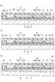
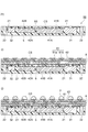
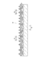
- FIG. 2, FIG. 3 and FIG. 4 are process diagrams showing one embodiment of a method for manufacturing an electronic component device including a plurality of electronic components including an IC chip and chip-type passive components.
- the composite base material 1 shown in FIG. 1 (a) is prepared.
- the composite base material 1 includes a support 11, a temporary fixing material layer 13, and a curable adhesive layer 15.
- the temporary fixing material layer 13 and the adhesive layer 15 are laminated in this order on the support 11.
- the support 11 may have sufficient strength and rigidity to support electronic components, and its material is not particularly limited.
- the support 11 may be a silicon wafer, a glass plate, or a stainless steel plate.
- the thickness of the support 11 is not particularly limited, but may be, for example, 200 to 2000 ⁇ m.
- An alignment mark for positioning the electronic component may be provided on the surface of the support 11 on the temporary fixing material layer 13 side.
- the alignment mark can be formed by using any material such as metal and resin. When the alignment mark is provided, the temporary fixing material layer 13 and the adhesive layer 15 may be transparent enough to make the alignment mark visible.
- the adhesive layer 15 contains a curable adhesive that irreversibly adheres to the adherend after curing.
- the thickness of the adhesive layer 15 may be, for example, 1 to 50 ⁇ m.
- the curable adhesive forming the adhesive layer 15 may be selected from those known as adhesives for semiconductors (see, for example, International Publication No. 2017/073630 and Japanese Patent No. 3117971).
- the curable adhesive forming the adhesive layer 15 contains, for example, a thermosetting resin and its curing agent.
- Thermosetting resin is a compound that can form a crosslinked structure by heating.
- the thermosetting resin may have a molecular weight of 10,000 or less.
- thermosetting resins include epoxy resins and acrylic resins.
- the curing agent is a compound that reacts with the thermosetting resin to form a crosslinked structure together with the thermosetting resin, or a compound that initiates a reaction in which the thermosetting resin forms a crosslinked structure.
- the curing agent include phenol resin curing agents, acid anhydride curing agents, amine curing agents, imidazole curing agents, phosphine curing agents, azo compounds and organic peroxides.
- the curable adhesive may further contain other components such as a thermoplastic resin and a filler (eg silica).
- the temporary fixing material layer 13 has releasability such that it can be peeled from the adhesive layer 15 after curing.
- the thickness of the temporary fixing material layer 13 may be, for example, 1 to 100 ⁇ m.
- the material forming the temporary fixing material layer 13 can be selected from the materials used for the purpose of temporary fixing or temporary bonding in the manufacture of the electronic component device (see, for example, Patent Document 1).
- the composite base material 1 can be obtained by, for example, a method of sequentially forming the temporary fixing material layer 13 and the adhesive layer 15 on the support 11.
- the film-shaped temporary fixing material layer 13 and the adhesive layer 15 may be prepared, respectively, and these may be sequentially laminated by thermocompression bonding. At this time, the film-shaped temporary fixing material layer 13 and the adhesive layer 15 may be laminated under reduced pressure from the viewpoint of preventing the entrainment of air bubbles.
- a laminated film having the temporary fixing material layer 13 and the adhesive layer 15 may be prepared in advance, and the laminated film may be laminated on the composite substrate 1.
- FIG. 1A shows a step of arranging the conductor precursor 21a for pattern formation on the adhesive layer 15 of the prepared composite base material 1.
- the pattern of the conductor precursor 21a includes a portion where a passive component described later is arranged.
- the conductor precursor 21a can be arranged on the adhesive layer 15 by a printing method such as screen printing.
- the conductor precursor 21a may be cured by heating to form a conductor, and can be arbitrarily selected from the conductor precursors usually used by those skilled in the art.
- the conductor precursor 21a may be a curable conductive paste containing conductive particles such as various metal particles or carbon particles.
- the conductor precursor may be a transitional liquid phase sintered metal adhesive containing metal particles capable of transitional liquid phase sintering. Details of the transitional liquid-phase sintered metal adhesive will be described later.
- FIG. 1B shows a step of mounting the chip-type passive components 31 and 32 on the conductor precursor 21a.
- the passive components 31 and 32 are selected according to the design of the electronic component device, but may be, for example, a resistor, a capacitor, or a combination thereof.
- the passive components 31 and 32 can be mounted on the conductor precursor 21a using a normal chip mounting machine.
- FIG. 1C shows a process of placing the IC chips 41 and 42 on the adhesive layer 15.
- the IC chips 41 and 42 are so-called face-down type chip components having a main body 41A or 42A and a plurality of bumps 41B or 42B arranged on one main surface side of the main body 41A or 42A.
- the IC chips 41 and 42 are arranged on the adhesive layer 15 so that the bumps 41B or 42B functioning as connecting portions are in contact with the adhesive layer 15.
- the tips of the bumps 41B and 42B may be partially embedded in the adhesive layer 15.
- the IC chips 41 and 42 may be arranged on the adhesive layer 15 in a state where the body portions 41A and 42A and the adhesive layer 15 are separated from each other.
- the IC chips 41 and 42 can be mounted on the adhesive layer 15 by using, for example, a chip mounting machine having a stage and a mounting head. By adjusting conditions such as the temperature and pressure of the stage and the mounting head, a part of the tip portions of the bumps 41B and 42B can be embedded in the adhesive layer 15.
- the order of arranging the passive components 31, 32 and the IC chips 41, 42 on the adhesive layer 15 can be arbitrarily changed. After the passive components 31 and 32 and the IC chips 41 and 42 are arranged on the adhesive layer 15, the adhesive layer 15 is cured. At the time when the passive components 31, 32 and the IC chips 41, 42 are arranged on the adhesive layer 15, the adhesive layer 15 may be the B stage. The adhesive layer 15 is often cured by heating. The cured adhesive layer 15 firmly fixes the passive components 31 and 32 and the IC chips 41 and 42 to the composite base material 1.
- the conductor precursor 21a on which the passive components 31 and 32 are placed is heated, whereby the conductive pattern 21 which is a cured body of the conductor precursor 21a. Is formed.
- the passive components 31 and 32 are fixed with the conductive pattern 21 interposed between the passive components 31 and 32 and the adhesive layer 15.
- FIG. 1D shows a step of forming the sealing layer 5 for sealing the IC chips 41 and 42 and the passive components 31 and 32 on the adhesive layer 15.
- the sealing layer 5 is formed so as to cover the entire IC chips 41 and 42 and the passive components 31 and 32, and also to fill the gap between these electronic components and the adhesive layer 15. However, the gap does not have to be completely filled.
- the sealing layer 5 can be formed in the mold by, for example, a compression type or transfer type molding machine.
- the sealing layer 5 may be formed using a film-shaped sealing material (see, for example, International Publication No. 2015/186744). In that case, from the viewpoint of preventing the entrainment of air bubbles, the film-shaped sealing material may be laminated under reduced pressure.
- FIG. 2E shows a step of forming a via hole 5A extending from the surface 5S of the sealing layer 5 opposite to the adhesive layer 15 toward the adhesive layer 15 in the sealing layer 5.
- the via hole 5A may completely penetrate the sealing layer 5, or the sealing layer 5 may remain at the bottom of the via hole 5A.
- the via hole 5A may be formed by an imprint method in which the mold is pressed against the surface 5S of the sealing layer 5 opposite to the adhesive layer 15. In the imprint method, a mold having a protrusion corresponding to the via hole 5A is used. The protrusions of the mold may be pressed against the surface 5S while heating the adhesive layer 15, the mold, or both. Usually, after the via holes 5A are formed, the sealing layer 5 is cured by heating.
- 2F shows a step of forming the conductive via 22 by filling the via hole 5A with a conductive material precursor for a conductive via and then heating the conductive material precursor in the via hole 5A.
- the method of filling the via hole 5A with the conductor precursor may be a printing method such as screen printing.
- the conductor precursor may be filled in the via hole 5A by printing a plurality of times.
- the conductor precursor may be filled in the via hole 5A under reduced pressure.
- the maximum width W of the via hole 5A or the conductive via 22 may be, for example, 10 to 200 ⁇ m.
- the height H of the via hole 5A or the conductive via 22 may be, for example, 30 to 500 ⁇ m. Even if the height H of the conductive via 22 is large, in other words, even if the aspect ratio of the conductive via 22 is large, the conductive via 22 can be efficiently processed by the imprint method and the method using the conductor precursor. Can be formed.
- the conductor precursor for the conductive via may be a conductive paste containing a plurality of metal particles and an organic binder in which the plurality of metal particles are dispersed.
- the conductive paste as the conductive precursor may be a transitional liquid phase sintered metal adhesive containing a plurality of metal particles capable of transitional liquid phase sintering. In this case, by sintering the conductive paste, a plurality of metal particles are fused with each other, thereby forming a conductive via 22 which is an electric body containing the metal sintered body.
- transition liquid phase sintering Transient Liquid Phase Sintering
- TLPS Transition liquid phase sintering
- TLPS Transition liquid phase sintering
- the melting point of the formed metal sintered body can exceed the heating temperature for sintering.
- the temporary fixing material layer 13 tends to be peeled off from the adhesive layer 15 particularly easily.
- a plurality of metal particles capable of transitional liquid phase sintering may include a combination of a high melting point metal and a low melting point metal.
- the plurality of metal particles may separately contain a first metal particle containing a high melting point metal particle and a second metal particle containing a low melting point metal, or the high melting point metal and the low melting point metal may be included. It may be contained in one metal particle.
- the conductive via 22 is formed by heating the conductor precursor to a liquid phase transition temperature of the plurality of metal particles or higher. be able to.
- the liquid phase transition temperature is determined by heating a plurality of metal particles from 25 ° C. to 300 ° C. at a heating rate of 10 ° C./min under a nitrogen stream of 50 ml / min by DSC (Differential scanning calorimetry). It can be measured under the conditions to be used.
- the temperature of the liquid phase transition observed at the lowest temperature is considered to be the liquid phase transition temperature of the metal particles.
- the liquid phase transition temperature of the Sn-3.0Ag-0.5Cu alloy is 217 ° C.
- a plurality of metal particles capable of transitional liquid phase sintering include a combination of a first metal particle containing a metal having a high melting point and a second metal particle containing a metal having a low melting point
- the second metal particle is used.
- the mass ratio of the first metal particles may be 2.0 to 4.0, or 2.2 to 3.5.
- Metal particles containing a metal having a high melting point and a metal having a low melting point can be obtained, for example, by forming a layer containing the other metal on the surface of the metal particles containing one metal by plating, vapor deposition, or the like. Metal particles containing one metal and metal particles containing the other metal may be composited by collision or the like.
- the high melting point metal may be at least one selected from the group consisting of Au, Cu, Ag, Co and Ni.
- the low melting point metal may be In, Sn, or a combination thereof. Examples of combinations of high melting point metal and low melting point metal are Au and In combination, Cu and Sn combination, Ag and Sn combination, Co and Sn combination, and Ni and Sn combination. Combinations can be mentioned.
- the combination of Cu and Sn produces a copper-tin metal compound (Cu 6 Sn 5 ) by sintering. Since this reaction proceeds at around 250 ° C., the conductor precursor containing a combination of Cu and Sn can be sintered by heating using a general facility such as a reflow oven.
- Sn can be contained in the metal particles as a simple substance of Sn metal or as an alloy containing Sn. Examples of alloys containing Sn include Sn-3.0Ag-0.5Cu alloys. The Sn-3.0Ag-0.5Cu alloy contains 3.0% by mass of Ag and 0.5% by mass of Cu based on the mass of the alloy.
- the content of the metal particles in the conductor precursor may be 80% by mass or more, 85% by mass or more, or 88% by mass or more, and 98% by mass or less, based on the mass of the conductor precursor. May be good.
- the content here is a ratio based on the total mass of the components other than the solvent when the conductor precursor contains a solvent described later.
- the average particle size of the metal particles may be 0.5 ⁇ m to 80 ⁇ m, 1 ⁇ m to 50 ⁇ m, or 1 ⁇ m to 30 ⁇ m.
- the average particle size here refers to the volume average particle size measured by a laser diffraction type particle size distribution meter (for example, Beckman Coulter Co., Ltd., LS 13 320 type laser scattering diffraction method particle size distribution measuring device).
- the organic binder in the conductor precursor may contain a thermoplastic resin.
- the thermoplastic resin may have a softening point lower than the liquid phase transition temperature of the metal particles.
- the softening point of the thermoplastic resin is a value measured by thermomechanical analysis.
- the softening point measured by the thermomechanical analysis method was that a 100 ⁇ m thick film obtained by forming a thermoplastic resin was compressed at a stress of 49 mN in the thickness direction while heating at a temperature rising rate of 10° C./min. Occasionally, it is the temperature at the time when a displacement of 80 ⁇ m was observed.
- a thermomechanical analyzer (TMA8320, manufactured by Rigaku Co., Ltd., measuring probe: compression weighting standard type) is used.
- the softening point of the thermoplastic resin may be a temperature 5 ° C. or higher lower than the liquid phase transition temperature of the metal particles, a temperature 10 ° C. or higher lower, or a temperature 15 ° C. or higher lower.
- the softening point of the thermoplastic resin may be 40°C or higher, 50°C or higher, or 60°C or higher.
- the thermoplastic resin may contain at least one selected from the group consisting of, for example, a polyamide resin, a polyamide-imide resin, a polyimide resin, and a polyurethane resin.
- the thermoplastic resin may contain a polyoxyalkylene group or a polysiloxane group.
- the polyoxyalkylene group may be a polyoxyethylene group, a polyoxypropylene group, or a combination thereof.
- the thermoplastic resin may be at least one resin selected from the group consisting of a polyamide resin, a polyamide-imide resin, a polyimide resin, and a polyurethane resin, which contains a polyoxyalkylene chain or a polysiloxane chain.
- a diamine compound having a polyoxyalkylene group or a polysiloxane group, or a diol compound having a polyoxyalkylene group or a polysiloxane group as a monomer, a polyoxyalkylene group or a polysiloxane group can be contained in these resins. Can be introduced.
- the content of the thermoplastic resin in the conductor precursor may be 5 to 30% by mass, 6 to 28% by mass, or 8 to 25% by mass based on the mass of the conductor precursor.
- the content here is a ratio based on the total mass of the components other than the solvent when the conductor precursor contains a solvent described later.
- the organic binder may contain a solvent, and may contain a solvent and a thermoplastic resin.
- the solvent may be a polar solvent.
- the boiling point of the solvent may be 200° C. or higher, or 300° C. or lower.
- solvents examples include terpineol, stearyl alcohol, tripropylene glycol methyl ether, diethylene glycol, diethylene glycol monoethyl ether (ethoxyethoxyethanol), diethylene glycol monohexyl ether, diethylene glycol monomethyl ether, dipropylene glycol-n-propyl ether, dipropylene glycol.
- Alcohols such as -n-butyl ether, tripropylene glycol-n-butyl ether, 1,3-butanediol, 1,4-butanediol, propylene glycol phenyl ether, and 2- (2-butoxyethoxy) ethanol; tributyl citrate, Esters such as ⁇ -butyrolactone, diethylene glycol monoethyl ether acetate, dipropylene glycol methyl ether acetate, diethylene glycol monobutyl ether acetate, and glycerin triacetate; ketones such as isophorone; lactams such as N-methyl-2-pyrrolidone; nitriles such as phenylacethide 4-Methyl-1,3-dioxolan-2-one; and sulfolane can be mentioned. You may use a solvent individually by 1 type or in combination of 2 or more types.
- the content of the solvent may be 0.1 to 10% by mass, 2 to 7% by mass, or 3 to 5% by mass based on the mass of the conductor precursor.
- the organic binder in the conductor precursor may further contain other components such as a thermosetting resin, a rosin, an activator, and a thixotropic agent.
- thermosetting resins include epoxy resins, oxazine resins, bismaleimide resins, phenol resins, unsaturated polyester resins and silicone resins.
- epoxy resins include bisphenol A type epoxy resin, bisphenol F type epoxy resin, bisphenol S type epoxy resin, phenol novolac type epoxy resin, cresol novolac type epoxy resin, naphthalene type epoxy resin, biphenol type epoxy resin, biphenyl novolac type. Examples thereof include epoxy resins and cyclic aliphatic epoxy resins.
- rosin examples include dehydroabietic acid, dihydroabietic acid, neoabietic acid, dihydropimaric acid, pimaric acid, isopimaric acid, tetrahydroabietic acid, and parastoric acid.
- activators include aminodecanoic acid, pentane-1,5-dicarboxylic acid, triethanolamine, diphenylacetic acid, sebacic acid, phthalic acid, benzoic acid, dibromosalicylic acid, anisic acid, iodosalicylic acid, and picolinic acid. ..
- thixo agents examples include 12-hydroxystearic acid, 12-hydroxystearic acid triglyceride, ethylene bisstearic acid amide, hexamethylene bisoleic acid amide, and N, N'-distearyl adipic acid amide.
- the conductor precursor can be obtained by mixing the metal particles and the components constituting the organic binder.
- the device for mixing may be, for example, a three-roll mill, a planetary mixer, a planetary mixer, a rotating / revolving stirrer, a scavenger, a twin-screw kneader, or a thin-layer shear disperser.
- FIG. 2 (g) shows a sealing structure 50 having an adhesive layer 15, passive components 31, 32, IC chips 41, 42, and a sealing layer 5 by peeling the temporary fixing material layer 13 from the adhesive layer 15. The process of obtaining.
- the resurface layer on one main surface side of the sealing structure 50 is the adhesive layer 15.
- the temporary fixing material layer 13 can be peeled from the adhesive layer 15 by, for example, heating, light irradiation, or mechanical peeling. A part of the adhesive layer 15 may be separated and removed together with the temporary fixing material layer 13.
- the sealing structure 50 is ground from the adhesive layer 15 side to remove the adhesive layer 15, whereby the sealing layer 5, the conductive pattern 21, the bumps 41B and 42B and the conductive via 22 are removed. Shows the process of forming the exposed circuit surface CS. Grinding of the sealing structure 50 can be performed using a normal grinding device. Part of the sealing layer 5, the conductive pattern 21, the bumps 41B and 42B, and the conductive via 22 may be ground.
- FIG. 3I shows a rewiring layer having a wiring 61 connected to the conductive pattern 21, the bumps 41B and 42B, and the conductive via 22, and an insulating layer 62 (insulating film) provided between the wirings 61.
- the step of providing or forming 6 on the circuit surface CS is shown.
- the wiring 61 includes a multilayer wiring layer 61a extending in a direction parallel to the main surface of the rewiring layer 6 and a connecting portion 61b extending in a direction perpendicular to the main surface of the rewiring layer 6.
- the thickness of each wiring layer 61a is not particularly limited, but may be 1 to 30 ⁇ m, for example.
- the rewiring layer 6 can be formed by a conventional method known to those skilled in the art. For the method of forming the redistribution layer, for example, Japanese Patent No. 5494766 can be referred to.
- FIG. 3J shows a step of arranging the solder balls 7 connected to the wiring 61 on the rewiring layer 6.
- the solder ball 7 is used as a connection terminal for secondary mounting. Reflow is performed if necessary.
- FIG. 4 shows a step of covering the surface of the sealing layer 5 opposite to the circuit surface CS to form the conductive shield film 23 connected to the conductive via 22.
- the shield film 23 is provided mainly for the purpose of electromagnetic wave shielding.
- the shield film 23 can be a single-layer or multi-layer metal thin film, and these can be formed by a method such as sputtering or vapor deposition.
- the shield film 23 may be formed using the same conductor precursor as that used for the conductive pattern 21 or the conductive via 22.
- the electronic component device 100 includes a sealing structure 50 including the passive components 31, 32, the IC chips 41, 42, the sealing layer 5, the conductive via 22, and the shield film 23, the passive components 31, 32, and the IC chip 41. , 42 and a rewiring layer 6 connected to it. It is also possible to collectively form a plurality of electronic component devices using one composite base material 1 and divide them.
- a rewiring structure having a rewiring layer is separately prepared, and the rewiring structure and the sealing structure are connected to each other to form a circuit surface.
- a rewiring layer can also be provided on top.
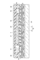
- the rewiring layer 6 having two main surfaces facing each other on the carrier base material 1B, and the main material on the opposite side of the rewiring layer 6 from the carrier base material 1B.
- a rewiring structure 60 having a plurality of bumps 63 provided on the surface is formed.
- the carrier base material 1B includes a support 11 and a temporary fixing material layer 13 provided on the support 11.
- the support 11 and the temporary fixing material layer 13 of the carrier base material 1B can have the same configuration as the support 11 and the temporary fixing material layer 13 of the composite base material 1.
- the rewiring layer 6 has a wiring 61 and an insulating layer 62 provided between the wirings 61.
- the wiring 61 includes a multilayer wiring layer 61a extending in a direction parallel to the main surface of the rewiring layer 6 and a connecting portion 61b extending in a direction perpendicular to the main surface of the rewiring layer 6.
- the thickness of each wiring layer 61a is not particularly limited, but may be 1 to 30 ⁇ m, for example.
- the redistribution layer 6 can be formed by a usual method known to those skilled in the art, like the redistribution layer of FIG.
- the bump 63 has, for example, a columnar portion 63a in contact with the wiring 61 and a hemispherical portion 63b provided on the columnar portion 63a.
- the columnar portion 63a may be formed of copper and the hemispherical portion 63b may be formed of lead-free solder (for example, an alloy containing Sn and Ag).
- the size of the bump 63 is adjusted within a range that ensures an appropriate connection with the wiring 61.
- the width of the bump 63 may be 5 to 100 ⁇ m and the height of the bump 63 may be 5 to 50 ⁇ m.
- the bump 63 can be formed by a conventional method.
- the prepared rewiring structure 60 may be inspected.
- the inspection includes, for example, checking whether or not there is an abnormality due to disconnection or short circuit of the wiring 61 and the bump 63.
- a defective product of the rewiring structure 60 can be excluded before the rewiring structure 60 is connected to the sealing structure 50.
- normal electronic components are less likely to be eliminated due to defects in the formation of rewiring, as compared to forming rewiring directly on the electronic components sealed in the sealing layer. be able to.
- FIG. 6 shows an example of a process of connecting the sealing structure 50 and the rewiring structure 60 with the insulating adhesive layer 70 interposed therebetween.
- the sealing structure 50 and the rewiring structure 60 are bonded to each other with the circuit surface CS and the bump 63 facing each other with the insulating adhesive layer 70 interposed therebetween.
- the sealing structure 50 and the rewiring structure 60 are aligned so that the connecting portion (conductive pattern 21 and bumps 41B and 42B) and a part of the plurality of bumps 63 are connected.
- the wiring 61 is connected to the connection portion ((the conductive pattern 21 and the bumps 41B and 42B) via the bump 63.
- connection portion (the conductive pattern 21 and the bumps 41B and 42B) and the bump 63,
- the sealing structure 50 and the rewiring structure 60 may be bonded together while heating and pressurizing for curing or both of the insulating adhesive layer 70.
- the heating temperature is, for example, 250 to 300 ° C. It may be present, and the pressure may be 0.5 to 1 MPa. It is sealed by connecting the connection portion (conductive pattern 21 and bumps 41B and 42B) and a part of the plurality of bumps 63.
- the structure 50 and the rewiring structure 60 are connected.
- the expression "connected” may mean “electrically connected”.
- the insulating adhesive layer 70 can be the same as a semiconductor adhesive that is usually used for adhering a semiconductor chip or the like to a circuit board.
- the insulating adhesive layer 70 may include the same curable adhesive as the adhesive layer 15.
- the insulating adhesive layer 70 may be arranged on the circuit surface CS of the sealing structure 50.
- a support film and a laminated film having an insulating adhesive layer provided on the support film may be prepared, and the insulating adhesive layer may be laminated on the circuit surface CS.
- An example of a commercially available laminated film that can be used for this purpose is the NCF AK series manufactured by Hitachi Chemical Company, Ltd.
- FIG. 7 shows an example of a step of peeling the carrier base material 1B from the rewiring structure 60 connected to the sealing structure 50.
- the temporary fixing material layer 13 of the carrier substrate 1B can be peeled from the rewiring layer 6 by, for example, heating, light irradiation, or mechanical peeling.
- solder ball 7 connected to the wiring 61 may be provided on the main surface of the rewiring layer 6 on the opposite side of the sealing structure 50. Good.
- the solder ball 7 is used as a connection terminal for secondary mounting. Reflow is performed if necessary.
- the electronic component device 101 can be obtained by the method exemplified above.
- the electronic component device 100 is mainly composed of a sealing structure 50, a rewiring structure 60, and an insulating adhesive layer 70 that is interposed between the sealing structure 50 and the rewiring structure 60 and adheres them. Will be done.
- the method of manufacturing the electronic component device is not limited to the examples described above, and can be changed if necessary.
- the conductive via 22 or the shield film 23 may not be provided.
Landscapes
- Physics & Mathematics (AREA)
- Wire Bonding (AREA)
- Production Of Multi-Layered Print Wiring Board (AREA)
- Laminated Bodies (AREA)
- Health & Medical Sciences (AREA)
- Manufacturing & Machinery (AREA)
- Engineering & Computer Science (AREA)
- Electromagnetism (AREA)
- Toxicology (AREA)
- Geometry (AREA)
- Encapsulation Of And Coatings For Semiconductor Or Solid State Devices (AREA)
- Structures Or Materials For Encapsulating Or Coating Semiconductor Devices Or Solid State Devices (AREA)
- Adhesive Tapes (AREA)
- Apparatuses And Processes For Manufacturing Resistors (AREA)
Abstract
支持体、仮固定材層、及び接着層を備える複合基材の接着層上に、複数の電子部品を、接着層に接する接続部を接着層と電子部品との間に介在させながら配置する工程と、接着層を硬化させることにより、複数の電子部品を複合基材に対して固定する工程と、電子部品を封止する封止層を形成する工程と、仮固定材層を接着層から剥離することにより、封止構造体を得る工程と、封止構造体を接着層側から研削することにより回路面を形成する工程とを含む、電子部品を製造する方法が開示される。複数の電子部品が、ICチップ、及びチップ型の受動部品を含む。受動部品が、パターン形成用の導電体前駆体を接続部として接着層上に配置することと、導電体前駆体上に受動部品を載せることと、導電体前駆体を加熱することによって導電パターンを接続部として形成することと、をこの順で含む方法により、接着層上に配置される。
Description
本発明は、電子部品装置を製造する方法、及びこれに用いられる積層フィルムに関する。
複数の半導体チップを有する半導体パッケージを製造する方法として、キャリア基板上に設けられた仮接着剤層上に半導体チップ(ダイ)を配列し、半導体チップを封止した後、キャリア基板を剥離する方法が知られている(例えば、特許文献1)。
ICチップ及び受動部品を有する複合的な電子部品装置も、仮接着剤層のような仮固定材層上にこれら構成部品を一時的に固定した状態で封止層を形成し、その後、仮固定材層を剥離する方法により、効率的に製造できることが期待される。
しかし、封止層を形成する工程の間に、ICチップ及び受動部品が所定の位置から移動するという、いわゆるダイシフトの問題がある。特に、サイズ及び高さの異なる複数種の電子部品を一括して封止する場合、ダイシフトの問題がより顕在化する懸念がある。そこで、本発明の一側面は、電子部品装置の製造におけるダイシフトを抑制する方法を提供する。
本発明の一側面は、ICチップ、及びチップ型の受動部品を含む複数の電子部品を備える電子部品装置を製造する方法に関する。本発明の一側面に係る方法は、
支持体、仮固定材層、及び硬化性の接着層を備え、これらがこの順に積層されている、複合基材を準備する工程と、
前記複合基材の前記接着層上に、複数の電子部品を、前記接着層に接する接続部を前記接着層と前記電子部品との間に介在させながら配置する工程と、
前記接着層を硬化させることにより、前記複数の電子部品を前記複合基材に対して固定する工程と、
前記電子部品を封止する封止層を前記接着層上に形成する工程と、
前記封止層を硬化させる工程と、
前記仮固定材層を前記接着層から剥離することにより、前記接着層、前記電子部品及び前記封止層を有する封止構造体を得る工程と、
前記封止構造体を前記接着層側から研削することにより、前記封止層及び前記接続部が露出した回路面を形成する工程と、を含む。
支持体、仮固定材層、及び硬化性の接着層を備え、これらがこの順に積層されている、複合基材を準備する工程と、
前記複合基材の前記接着層上に、複数の電子部品を、前記接着層に接する接続部を前記接着層と前記電子部品との間に介在させながら配置する工程と、
前記接着層を硬化させることにより、前記複数の電子部品を前記複合基材に対して固定する工程と、
前記電子部品を封止する封止層を前記接着層上に形成する工程と、
前記封止層を硬化させる工程と、
前記仮固定材層を前記接着層から剥離することにより、前記接着層、前記電子部品及び前記封止層を有する封止構造体を得る工程と、
前記封止構造体を前記接着層側から研削することにより、前記封止層及び前記接続部が露出した回路面を形成する工程と、を含む。
前記複数の電子部品が、ICチップ、及びチップ型の受動部品を含む。前記ICチップが、本体部、及び該本体部の一方の主面側に設けられたバンプを有する。前記ICチップが、前記接続部としての前記バンプが前記接着層に接する向きで前記接着層上に配置される。前記受動部品が、パターン形成用の導電体前駆体を前記接続部として前記接着層上に配置することと、前記導電体前駆体上に前記受動部品を載せることと、前記導電体前駆体を加熱することによって導電パターンを前記接続部として形成することと、をこの順に含む方法により、前記接着層上に配置される。
本発明の別の一側面は、仮固定材層、及び前記仮固定材層上に設けられた硬化性の接着層を有し、上記方法において前記複合基材を準備するために用いられる、電子部品装置製造用積層フィルムに関する。
本発明の一側面に係る方法では、硬化した接着層によって電子部品が複合基材に対して固定された状態で、封止層が形成されるため、電子部品が移動し難い。
以下、本発明のいくつかの実施形態について詳細に説明する。ただし、本発明は以下の実施形態に限定されるものではない。
図1、図2、図3及び図4は、ICチップ、及びチップ型の受動部品を含む複数の電子部品を備える電子部品装置を製造する方法の一実施形態を示す工程図である。
図1の(a)に示される複合基材1が準備される。複合基材1は、支持体11、仮固定材層13、及び硬化性の接着層15を備える。支持体11上に仮固定材層13及び接着層15がこの順に積層されている。
支持体11は、電子部品を支持可能な程度の強度及び剛性を有していればよく、その材質は特に限定されない。例えば、支持体11が、シリコンウェハ、ガラス板、又はステンレス鋼板であってもよい。支持体11の厚さは、特に制限されないが、例えば200~2000μmであってもよい。支持体11の仮固定材層13側の面上に、電子部品の位置決めのためのアライメントマークが設けられてもよい。アライメントマークは、金属、樹脂等の任意の材料を用いて形成することができる。アライメントマークが設けられる場合、仮固定材層13及び接着層15が、アライメントマークを視認可能な程度に透明であってもよい。
接着層15は、硬化後、被着体に不可逆的に接着する硬化性接着剤を含む。接着層15の厚さは、例えば1~50μmであってもよい。接着層15を形成する硬化性接着剤を、半導体用接着剤として知られるものから選択してもよい(例えば、国際公開第2017/073630号、及び特許第3117971号公報参照)。
接着層15を形成する硬化性接着剤は、例えば、熱硬化性樹脂及びその硬化剤を含有する。熱硬化性樹脂は、加熱により架橋構造を形成し得る化合物である。熱硬化性樹脂は10000以下の分子量を有していてもよい。熱硬化性樹脂の例としては、エポキシ樹脂、及びアクリル樹脂が挙げられる。硬化剤は、熱硬化性樹脂と反応して、熱硬化性樹脂とともに架橋構造を形成する化合物、又は、熱硬化性樹脂が架橋構造を形成する反応を開始させる化合物である。硬化剤としては、例えば、フェノール樹脂系硬化剤、酸無水物系硬化剤、アミン系硬化剤、イミダゾール系硬化剤、ホスフィン系硬化剤、アゾ化合物及び有機過酸化物が挙げられる。硬化性接着剤が、熱可塑性樹脂、フィラー(例えばシリカ)等のその他の成分を更に含有してもよい。
仮固定材層13は、硬化後の接着層15から剥離できる程度の剥離性を有する。仮固定材層13の厚さは、例えば1~100μmであってもよい。仮固定材層13を形成する材料は、電子部品装置の製造において、仮固定又は仮接着の目的で用いられている材料から選択することができる(例えば、特許文献1参照)。
複合基材1は、例えば、支持体11上に仮固定材層13、及び接着層15を順に形成する方法によって得ることができる。フィルム状の仮固定材層13及び接着層15をそれぞれ準備し、熱圧着によりこれらを順に積層してもよい。このとき、気泡の巻き込み防止の観点から減圧下でフィルム状の仮固定材層13及び接着層15を積層してもよい。あるいは、仮固定材層13及び接着層15を有する積層フィルムを予め作製し、その積層フィルムを複合基材1上に積層してもよい。
図1の(a)は、準備した複合基材1の接着層15上に、パターン形成用の導電体前駆体21aを配置する工程を示す。導電体前駆体21aのパターンは、後述の受動部品が配置される部分を含む。導電体前駆体21aは、例えば、スクリーン印刷のような印刷法によって接着層15上に配置することができる。
導電体前駆体21aは、加熱により硬化し、導電体を形成するものであってもよく、当業者に通常用いられている導電体前駆体から任意に選択できる。例えば、導電体前駆体21aが各種金属粒子又はカーボン粒子のような導電性粒子を含む硬化性の導電性ペーストであってもよい。導電体前駆体が、遷移的液相焼結が可能な金属粒子を含む遷移的液相焼結型金属接着剤であってもよい。遷移的液相焼結型金属接着剤の詳細については後述される。
図1の(b)は、導電体前駆体21a上にチップ型の受動部品31,32を載せる工程を示す。受動部品31,32は、電子部品装置の設計に従って選択されるが、例えば、抵抗、コンデンサ又はこれらの組み合わせであってもよい。受動部品31,32は、通常のチップ搭載機を用いて導電体前駆体21a上に載せることができる。
図1の(c)は、接着層15上にICチップ41及び42を載せる工程を示す。ICチップ41及び42は、本体部41A又は42Aと、本体部41A又は42Aの一方の主面側に配列された複数のバンプ41B又は42Bとを有する、いわゆるフェイスダウン型のチップ部品である。ICチップ41及び42は、接続部として機能するバンプ41B又は42Bが接着層15に接する向きで接着層15上に配置される。バンプ41B及び42Bの先端部が接着層15に部分的に埋め込まれてもよい。本体部41A,42Aと接着層15とが離れた状態で、ICチップ41,42が接着層15上に配置されてもよい。ICチップ41,42は、例えば、ステージ及び搭載ヘッドを有するチップ搭載機を用いて接着層15上に載せることができる。ステージ及び搭載ヘッドの温度及び圧力等の条件を調整することにより、バンプ41B及び42Bの先端部の一部を接着層15に埋め込むことができる。
受動部品31,32及びICチップ41,42を接着層15上に配置する順番は任意に変更することができる。受動部品31,32及びICチップ41,42が接着層15上に配置された後、接着層15が硬化される。受動部品31,32及びICチップ41,42が接着層15上に配置される時点では、接着層15がBステージであってもよい。接着層15は、加熱により硬化されることが多い。硬化した接着層15によって、受動部品31,32及びICチップ41,42が複合基材1に対して強固に固定される。接着層15の硬化と同時に、又は接着層15の硬化の後、受動部品31,32が載せられた導電体前駆体21aを加熱することにより、導電体前駆体21aの硬化体である導電パターン21が形成される。これにより、受動部品31,32が、受動部品31,32と接着層15との間に導電パターン21が介在している状態で固定される。
図1の(d)は、ICチップ41,42及び受動部品31,32を封止する封止層5を接着層15上に形成する工程を示す。封止層5は、ICチップ41,42及び受動部品31,32の全体を覆うとともに、これら電子部品と接着層15との間の隙間も充填するように形成される。ただし、隙間が完全に充填されなくてもよい。封止層5は、例えば、コンプレッション方式又はトランスファー方式の成形機によって、金型内で形成することができる。あるいは、フィルム状の封止材を用いて封止層5を形成してもよい(例えば、国際公開第2015/186744号参照。)。その場合、気泡の巻き込み防止の観点から、フィルム状の封止材を減圧下で積層してもよい。
図2の(e)は、封止層5の接着層15とは反対側の面5Sから接着層15に向けて延びるビア孔5Aを、封止層5内に形成する工程を示す。ビア孔5Aは封止層5を完全に貫通していてもよいし、ビア孔5Aの底部に封止層5が残存していてもよい。ビア孔5Aが、封止層5の接着層15とは反対側の面5Sに対してモールドを押し込むインプリント法によって形成されてもよい。インプリント法においては、ビア孔5Aに対応する突起部を有するモールドが用いられる。接着層15、モールド又はこれらの両方を加熱しながら、モールドの突起部を面5Sに対して押し込んでもよい。通常、ビア孔5Aが形成された後、封止層5が加熱により硬化される。
図2の(f)は、ビア孔5Aに導電性ビア用の導電体前駆体を充填し、その後、ビア孔5A内の導電体前駆体を加熱することにより、導電性ビア22を形成する工程を示す。導電体前駆体をビア孔5Aに充填する方法は、スクリーン印刷等の印刷法であってもよい。複数回の印刷により、導電体前駆体をビア孔5Aに充填してもよい。導電体前駆体を減圧下でビア孔5Aに充填してもよい。ビア孔5A内の導電体前駆体を加熱することにより、導電体前駆体の硬化体である導電性ビア22を形成することができる。
ビア孔5A又は導電性ビア22の最大幅Wは、例えば10~200μmであってもよい。ビア孔5A又は導電性ビア22の高さHは、例えば30~500μmであってもよい。導電性ビア22の高さHが大きいとき、言い換えると導電性ビア22のアスペクト比が大きいときであっても、インプリント法及び導電体前駆体を用いた方法により、効率的に導電性ビア22を形成することができる。
導電性ビア用の導電体前駆体が、複数の金属粒子及び該複数の金属粒子が分散した有機バインダーを含有する導電性ペーストであってもよい。導電性前駆体としての導電性ペーストが、遷移的液相焼結が可能な複数の金属粒子を含む、遷移的液相焼結型金属接着剤であってもよい。この場合、導電性ペーストの焼結により、複数の金属粒子同士が融合し、それにより金属焼結体を含む電体である導電性ビア22が形成される。ここで、「遷移的液相焼結」(Transient Liquid Phase Sintering)とは、TLPSとも称され、一般に、低融点金属の粒子界面における加熱による液相への転移と、形成された液相への高融点金属の反応拡散とにより進行する焼結をいう。遷移的液相焼結によれば、形成される金属焼結体の融点が、焼結のための加熱温度を上回ることができる。低温の加熱で導電性ビアを形成すると、仮固定材層13を接着層15から特に容易に剥離できる傾向がある。
遷移的液相焼結が可能な複数の金属粒子は、高融点の金属と低融点の金属との組み合わせを含んでいてもよい。複数の金属粒子が、高融点の金属粒子を含む第1の金属粒子及び低融点の金属を含む第2の金属粒子を別々に含んでいてもよいし、高融点の金属及び低融点の金属が1個の金属粒子中に含まれていてもよい。
導電体前駆体が遷移的液相焼結が可能な複数の金属粒子を含む場合、導電体前駆体を複数の金属粒子の液相転移温度以上に加熱することによって、導電性ビア22を形成することができる。液相転移温度は、DSC(Differential scanning calorimetry、示差走査熱量測定)により、50ml/分の窒素気流下にて、10℃/分の昇温速度で25℃から300℃まで複数の金属粒子を加熱する条件で測定することができる。金属粒子が複数種の金属を含む場合、最も低い温度で観測される液相転移の温度が、金属粒子の液相転移温度とみなされる。例えば、Sn-3.0Ag-0.5Cu合金の液相転移温度は217℃である。
遷移的液相焼結が可能な複数の金属粒子が高融点の金属を含む第1の金属粒子と低融点の金属を含む第2の金属粒子との組み合わせを含む場合、第2の金属粒子に対する第1の金属粒子の質量比が、2.0~4.0、又は2.2~3.5であってもよい。
高融点の金属及び低融点の金属を含有する金属粒子は、例えば、一方の金属を含む金属粒子の表面に、めっき、蒸着等により他方の金属を含む層を形成することにより得ることができる。一方の金属を含む金属粒子と他方の金属を含む金属粒子とを衝突等により複合化してもよい。
高融点の金属は、Au,Cu、Ag、Co及びNiからなる群より選ばれる少なくとも1種であってもよい。低融点の金属は、In、Sn又はこれらの組み合わせであってもよい。高融点の金属と低融点の金属との組み合わせの例としては、AuとInとの組み合わせ、CuとSnとの組み合わせ、AgとSnとの組み合わせ、CoとSnとの組み合わせ及びNiとSnとの組み合わせが挙げられる。
CuとSnとの組み合わせは、焼結によって銅-錫金属化合物(Cu6Sn5)を生成する。この反応は250℃付近で進行するため、CuとSnとを組み合わせを含む導電体前駆体は、リフロー炉等の一般的な設備を用いた加熱によって焼結することができる。Snは、Sn金属単体として、又はSnを含む合金として金属粒子に含まれることができる。Snを含む合金の例としては、Sn-3.0Ag-0.5Cu合金が挙げられる。Sn-3.0Ag-0.5Cu合金は、合金の質量を基準として、3.0質量%のAg及び0.5質量%のCuを含む。
導電体前駆体における金属粒子の含有量は、導電体前駆体の質量を基準として、80質量%以上、85質量%以上、又は88質量%以上であってもよく、98質量%以下であってもよい。ここでの含有量は、導電体前駆体が後述の溶剤を含む場合、溶剤以外の成分の合計質量を基準とする割合である。
金属粒子の平均粒径は、0.5μm~80μm、1μm~50μm、又は1μm~30μmであってもよい。ここでの平均粒径は、レーザー回折式粒度分布計(例えば、ベックマン・コールター株式会社、LS 13 320型レーザー散乱回折法粒度分布測定装置)によって測定される体積平均粒径をいう。
導電体前駆体中の有機バインダーは、熱可塑性樹脂を含んでいてもよい。熱可塑性樹脂が、金属粒子の液相転移温度よりも低い軟化点を有していてもよい。熱可塑性樹脂の軟化点は、熱機械分析法により測定される値をいう。熱機械的分析法によって測定される軟化点は、熱可塑性樹脂を成膜して得た厚み100μmフィルムを、昇温速度10℃/分にて加熱しながら、49mNの応力で厚み方向に圧縮したときに、80μmの変位が観測された時点の温度である。測定装置としては、例えば熱機械的分析装置(TMA8320、株式会社リガク製、測定用プローブ:圧縮加重法標準型)が用いられる。
熱可塑性樹脂の軟化点は、金属粒子の液相転移温度よりも5℃以上低い温度、10℃以上低い温度、又は15℃以上低い温度であってもよい。熱可塑性樹脂の軟化点は、40℃以上、50℃以上、又は60℃以上であってもよい。
熱可塑性樹脂は、例えば、ポリアミド樹脂、ポリアミドイミド樹脂、ポリイミド樹脂及びポリウレタン樹脂からなる群より選択される少なくとも1種を含んでもよい。熱可塑性樹脂が、ポリオキシアルキレン基又はポリシロキサン基を含んでもよい。ポリオキシアルキレン基は、ポリオキシエチレン基、ポリオキシプロピレン基又はこれらの組み合わせであってもよい。
熱可塑性樹脂が、ポリオキシアルキレン鎖又はポリシロキサン鎖を含む、ポリアミド樹脂、ポリアミドイミド樹脂、ポリイミド樹脂及びポリウレタン樹脂からなる群より選択される少なくとも1種の樹脂であってもよい。例えば、ポリオキシアルキレン基若しくはポリシロキサン基を有するジアミン化合物、又はポリオキシアルキレン基若しくはポリシロキサン基を有するジオール化合物を単量体として用いることにより、これら樹脂中にポリオキシアルキレン基又はポリシロキサン基を導入することができる。
導電体前駆体における熱可塑性樹脂の含有量は、導電体前駆体の質量を基準として、5~30質量%、6~28質量%、又は8~25質量%であってもよい。ここでの含有量は、導電体前駆体が後述の溶剤を含む場合、溶剤以外の成分の合計質量を基準とする割合である。
有機バインダーは、溶剤を含んでいてもよく、溶剤及び熱可塑性樹脂を含んでいてもよい。溶剤は極性溶媒であってもよい。溶剤の沸点は200℃以上であってもよく、300℃以下であってもよい。
溶剤の例としては、テルピネオール、ステアリルアルコール、トリプロピレングリコールメチルエーテル、ジエチレングリコール、ジエチレングリコールモノエチルエーテル(エトキシエトキシエタノール)、ジエチレングリコールモノヘキシルエーテル、ジエチレングリコールモノメチルエーテル、ジプロピレングリコール-n-プロピルエーテル、ジプロピレングリコール-n-ブチルエーテル、トリプロピレングリコール-n-ブチルエーテル、1,3-ブタンジオール、1,4-ブタンジオール、プロピレングリコールフェニルエーテル、及び2-(2-ブトキシエトキシ)エタノール等のアルコール;クエン酸トリブチル、γ-ブチロラクトン、ジエチレングリコールモノエチルエーテルアセテート、ジプロピレングリコールメチルエーテルアセテート、ジエチレングリコールモノブチルエーテルアセテート、及びグリセリントリアセテート等のエステル;イソホロン等のケトン;N-メチル-2-ピロリドン等のラクタム;フェニルアセトニトリル等のニトリル;4-メチル-1,3-ジオキソラン-2-オン;並びにスルホランを挙げることができる。溶剤は、1種類を単独で又は2種類以上を組み合わせて使用してもよい。
溶剤の含有量は、導電体前駆体の質量を基準として、0.1~10質量%、2~7質量%、又は3~5質量%であってもよい。
導電体前駆体中の有機バインダーは、熱硬化性樹脂、ロジン、活性剤、チキソ剤等のその他の成分を更に含んでいてもよい。
熱硬化性樹脂の例としては、例えば、エポキシ樹脂、オキサジン樹脂、ビスマレイミド樹脂、フェノール樹脂、不飽和ポリエステル樹脂及びシリコーン樹脂が挙げられる。エポキシ樹脂の例としては、ビスフェノールA型エポキシ樹脂、ビスフェノールF型エポキシ樹脂、ビスフェノールS型エポキシ樹脂、フェノールノボラック型エポキシ樹脂、クレゾールノボラック型エポキシ樹脂、ナフタレン型エポキシ樹脂、ビフェノール型エポキシ樹脂、ビフェニルノボラック型エポキシ樹脂及び環式脂肪族エポキシ樹脂が挙げられる。
ロジンの例としては、デヒドロアビエチン酸、ジヒドロアビエチン酸、ネオアビエチン酸、ジヒドロピマル酸、ピマル酸、イソピマル酸、テトラヒドロアビエチン酸、及びパラストリン酸が挙げられる。
活性剤の例としては、アミノデカン酸、ペンタン-1,5-ジカルボン酸、トリエタノールアミン、ジフェニル酢酸、セバシン酸、フタル酸、安息香酸、ジブロモサリチル酸、アニス酸、ヨードサリチル酸、及びピコリン酸が挙げられる。
チキソ剤の例としては、12-ヒドロキシステアリン酸、12-ヒドロキシステアリン酸トリグリセリド、エチレンビスステアリン酸アマイド、ヘキサメチレンビスオレイン酸アマイド、及びN,N’-ジステアリルアジピン酸アマイドが挙げられる。
導電体前駆体は、金属粒子と、有機バインダーを構成する成分とを混合することにより得ることができる。混合のための装置は、例えば、3本ロールミル、プラネタリーミキサ、遊星式ミキサ、自転公転型撹拌装置、らいかい機、二軸混練機、又は薄層せん断分散機であってもよい。
図2の(g)は、仮固定材層13を接着層15から剥離することにより、接着層15、受動部品31,32、ICチップ41,42及び封止層5を有する封止構造体50を得る工程を示す。封止構造体50の一方の主面側の再表層が、接着層15である。仮固定材層13は、例えば、加熱、光照射、又は機械剥離により、接着層15から剥離することができる。接着層15の一部が分離して、仮固定材層13とともに除去されてもよい。
図3の(h)は、封止構造体50を接着層15側から研削して接着層15を除去し、それにより、封止層5、導電パターン21、バンプ41B,42B及び導電性ビア22が露出した回路面CSを形成する工程を示す。封止構造体50の研削は、通常の研削装置を用いて行うことができる。封止層5、導電パターン21、バンプ41B,42B及び導電性ビア22の一部が研削されてもよい。
図3の(i)は、導電パターン21、バンプ41B,42B、及び導電性ビア22に接続された配線61と、配線61間に設けられた絶縁層62(絶縁膜)とを有する再配線層6を回路面CS上に設ける、又は形成する工程を示す。配線61は、再配線層6の主面に平行な方向に延在する多層の配線層61aと、再配線層6の主面に垂直な方向に延在する連結部61bとを含む。それぞれの配線層61aの厚さは、特に制限されないが、例えば1~30μmであってもよい。再配線層6は、当業者に知られる通常の方法によって形成することができる。再配線層を形成する方法に関しては、例えば、特許第5494766号公報を参照することができる。
図3の(j)は、配線61に接続されるはんだボール7を再配線層6上に配置する工程を示す。はんだボール7は二次実装用の接続端子として用いられる。必要によりリフローが行われる。
図4は、封止層5の回路面CSとは反対側の面を覆い、導電性ビア22と接続された導電性のシールド膜23を形成する工程を示す。これにより、目的とする電子部品装置100が得られる。シールド膜23は、主として電磁波シールドの目的で設けられる。シールド膜23は、単層又は複数層の金属薄膜であることができ、これらは例えばスパッタ又は蒸着のような方法によって形成することができる。シールド膜23を、導電パターン21又は導電性ビア22と同様の導電体前駆体を用いて形成してもよい。電子部品装置100は、受動部品31,32、ICチップ41,42、封止層5、導電性ビア22、及びシールド膜23を含む封止構造体50と、受動部品31,32及びICチップ41,42と接続された再配線層6とを備える。1枚の複合基材1上を用いて複数の電子部品装置を一括して形成し、それらを分割してもよい。
図5、図6、図7及び図8に例示されるように、再配線層を有する再配線構造体を別途準備し、再配線構造体と封止構造体とを接続することにより、回路面上に再配線層を設けることもできる。この方法の場合、例えば図5に示されるように、キャリア基材1B上に、対向する2つの主面を有する再配線層6と、再配線層6のキャリア基材1Bとは反対側の主面上に設けられた複数のバンプ63とを有する再配線構造体60が形成される。
キャリア基材1Bは、支持体11と、支持体11上に設けられた仮固定材層13とを備える。キャリア基材1Bの支持体11及び仮固定材層13は、複合基材1の支持体11及び仮固定材層13と同様の構成を有することができる。
再配線層6は、配線61と、配線61間に設けられた絶縁層62とを有する。配線61は、再配線層6の主面に平行な方向に延在する多層の配線層61aと、再配線層6の主面に垂直な方向に延在する連結部61bとを含む。それぞれの配線層61aの厚さは、特に制限されないが、例えば1~30μmであってもよい。再配線層6は、図3の再配線層と同様に、当業者に知られる通常の方法によって形成することができる。
バンプ63は、例えば、配線61と接する柱状部63aと柱状部63a上に設けられた半球部63bとを有する。柱状部63aが銅から形成され、半球部63bが鉛フリーはんだ(例えばSn及びAgを含む合金)から形成されていてもよい。バンプ63のサイズは、配線61との適切な接続が確保される範囲で調整される。例えば、バンプ63の幅が5~100μmで、バンプ63の高さが5~50μmであってもよい。バンプ63は通常の方法によって形成することができる。
準備された再配線構造体60を検査してもよい。検査は、例えば配線61及びバンプ63の断線又は短絡による異常の有無を確認することを含む。この検査により、再配線構造体60が封止構造体50と接続される前に、再配線構造体60の不良品を排除することができる。その結果、封止層内に封止された電子部品上に直接再配線を形成する場合と比較して、正常な電子部品が再配線の形成における不具合のために排除される可能性を低くすることができる。
図6は、封止構造体50と再配線構造体60とが絶縁性接着層70を介在させながら接続される工程の一例を示す。封止構造体50と再配線構造体60とが、回路面CSとバンプ63とが対向する向きで、絶縁性接着層70を介在させながら接着される。このとき、接続部(導電パターン21、及びバンプ41B,42B)と複数のバンプ63のうち一部とが接続されるように、封止構造体50及び再配線構造体60が位置合わせされる。これにより、配線61がバンプ63を介して接続部((導電パターン21、及びバンプ41B,42B)に接続される。接続部(導電パターン21、及びバンプ41B,42B)とバンプ63との接続、絶縁性接着層70の硬化、又はこれらの両方のために、加熱及び加圧しながら封止構造体50と再配線構造体60とを貼り合わせてもよい。加熱温度は、例えば250~300℃であってもよく、圧力は0.5~1MPaであってもよい。接続部(導電パターン21、及びバンプ41B,42B)と複数のバンプ63のうち一部とが接続されることにより、封止構造体50と再配線構造体60とが接続される。本明細書において、「接続される」という表現は、「電気的に接続される」ことを意味することがある。
絶縁性接着層70は、半導体チップ等を回路基板に接着するために通常用いられている半導体接着剤と同様のものであることができる。絶縁性接着層70が、接着層15と同様の硬化性接着剤を含んでいてもよい。封止構造体50と再配線構造体60とを接続する前に、封止構造体50の回路面CS上に絶縁性接着層70を配置してもよい。
支持フィルム及び支持フィルム上に設けられた絶縁性接着層を有する積層フィルムを準備し、その絶縁性接着層を回路面CS上に積層してもよい。そのために用いられ得る積層フィルムの市販品の例としては、日立化成株式会社製のNCF AKシリーズが挙げられる。
図7は、封止構造体50に接続された再配線構造体60からキャリア基材1Bを剥離する工程の一例を示す。キャリア基材1Bの仮固定材層13は、例えば、加熱、光照射、又は機械剥離により、再配線層6から剥離することができる。
キャリア基材1Bの剥離の後、図8に示されるように、再配線層6の封止構造体50とは反対側の主面上に、配線61と接続されるはんだボール7を設けてもよい。はんだボール7は二次実装用の接続端子として用いられる。必要によりリフローが行われる。
以上例示された方法によって、電子部品装置101が得られる。電子部品装置100は、封止構造体50と、再配線構造体60と、封止構造体50と再配線構造体60との間に介在しこれらを接着する絶縁性接着層70とから主として構成される。
電子部品装置を製造する方法は、以上説明した例に限定されるものではなく、必要により変更が可能である。例えば、導電性ビア22、又はシールド膜23が設けられなくてもよい。
1…複合基材、1B…キャリア基材、5…封止層、5A…ビア孔、6…再配線層、7…はんだボール、11…支持体、13…仮固定材層、15…接着層、21…導電パターン、21a…導電体前駆体、22…導電性ビア、23…シールド膜、31,32…受動部品、41,42…ICチップ、41A,42A…本体部、41B,42B…バンプ、50…封止構造体、60…再配線構造体、61…配線、62…絶縁層、63…バンプ、70…絶縁性接着層、100,101…電子部品装置、CS…回路面。
Claims (9)
- 支持体、仮固定材層、及び硬化性の接着層を備え、これらがこの順に積層されている、複合基材を準備する工程と、
前記複合基材の前記接着層上に、複数の電子部品を、前記接着層に接する接続部を前記接着層と前記電子部品との間に介在させながら配置する工程と、
前記接着層を硬化させることにより、前記複数の電子部品を前記複合基材に対して固定する工程と、
前記電子部品を封止する封止層を前記接着層上に形成する工程と、
前記封止層を硬化させる工程と、
前記仮固定材層を前記接着層から剥離することにより、前記接着層、前記電子部品及び前記封止層を有する封止構造体を得る工程と、
前記封止構造体を前記接着層側から研削することにより、前記封止層及び前記接続部が露出した回路面を形成する工程と、
をこの順で含み、
前記複数の電子部品が、ICチップ、及びチップ型の受動部品を含み、
前記ICチップが、本体部、及び該本体部の一方の主面側に設けられたバンプを有し、
前記ICチップが、前記接続部としての前記バンプが前記接着層に接する向きで前記接着層上に配置され、
前記受動部品が、パターン形成用の導電体前駆体を前記接続部として前記接着層上に配置することと、前記導電体前駆体上に前記受動部品を載せることと、前記導電体前駆体を加熱することによって導電パターンを前記接続部として形成することと、をこの順で含む方法により、前記接着層上に配置される、
電子部品装置を製造する方法。 - 当該方法が、
前記封止層の前記接着層とは反対側の面から前記接着層に向けて延びるビア孔を、前記封止層内に形成する工程と、
前記ビア孔に導電性ビア用の導電体前駆体を充填する工程と、
前記ビア孔内の前記導電体前駆体を加熱することにより、導電性ビアを形成する工程と、
を更に含み、
前記封止構造体が前記導電性ビアを更に有し、前記導電性ビアが前記封止層及び前記接続部とともに前記回路面に露出するように、前記封止構造体が前記接着層側から研削される、請求項1に記載の方法。 - 前記ビア孔が、前記封止層を硬化させる工程の前に、前記封止層の前記接着層とは反対側の面に対してモールドを押し込むインプリント法によって形成される、請求項2に記載の方法。
- 導電性ビア用の前記導電体前駆体が、複数の金属粒子及び該複数の金属粒子が分散した有機バインダーを含有し、
前記導電体前駆体が加熱されたときに、前記複数の金属粒子が、遷移的液相焼結により金属焼結体を形成し、それにより前記金属焼結体を含む前記導電性ビアが形成される、請求項2又は3に記載の方法。 - 当該方法が、前記封止層の前記接続部とは反対側の面を覆い、前記導電性ビアと接続された導電性のシールド膜を形成する工程を更に含む、請求項2~4のいずれか一項に記載の方法。
- 当該方法が、前記接続部に接続された配線を有する再配線層を前記回路面上に設ける工程を更に含む、請求項1~5のいずれか一項に記載の方法。
- 対向する2つの主面を有する前記再配線層と前記再配線層の一方の主面上に設けられた複数のバンプとを備える再配線構造体であって、前記配線が前記複数のバンプに接続されている、再配線構造体を準備することと、
前記封止構造体と前記再配線構造体とを、前記回路面と前記複数のバンプとが対向する向きで、絶縁性接着層を介在させながら、前記接続部と前記複数のバンプのうち少なくとも一部とが接続されるように接着し、それにより前記封止構造体と前記再配線構造体とを、前記配線が前記バンプを介して前記接続部に接続されるように接続することと、
を含む方法により、前記再配線層が前記回路面上に設けられる、請求項6に記載の方法。 - 前記再配線構造体が、支持体及び該支持体上に設けられた仮固定材層を備えるキャリア基材の前記仮固定材層上に設けられ、
当該方法が、前記再配線層を前記回路面上に設ける工程の後、前記キャリア基材を前記再配線構造体から剥離する工程を更に含む、請求項7に記載の方法。 - 仮固定材層、及び前記仮固定材層上に設けられた硬化性の接着層を有し、請求項1~8のいずれか一項に記載の方法において前記複合基材を準備するために用いられる、電子部品装置製造用積層フィルム。
Priority Applications (2)
| Application Number | Priority Date | Filing Date | Title |
|---|---|---|---|
| JP2020542475A JP6838686B2 (ja) | 2019-03-06 | 2020-03-05 | 電子部品装置を製造する方法、及びこれに用いられる積層フィルム |
| US17/435,623 US12183686B2 (en) | 2019-03-06 | 2020-03-05 | Method for producing electronic component device and laminated film used therefor |
Applications Claiming Priority (4)
| Application Number | Priority Date | Filing Date | Title |
|---|---|---|---|
| JP2019-040661 | 2019-03-06 | ||
| JP2019040661 | 2019-03-06 | ||
| PCT/JP2019/029888 WO2021019697A1 (ja) | 2019-07-30 | 2019-07-30 | 電子部品装置を製造する方法、及び電子部品装置 |
| JPPCT/JP2019/029888 | 2019-07-30 |
Publications (1)
| Publication Number | Publication Date |
|---|---|
| WO2020179875A1 true WO2020179875A1 (ja) | 2020-09-10 |
Family
ID=72337156
Family Applications (1)
| Application Number | Title | Priority Date | Filing Date |
|---|---|---|---|
| PCT/JP2020/009476 Ceased WO2020179875A1 (ja) | 2019-03-06 | 2020-03-05 | 電子部品装置を製造する方法、及びこれに用いられる積層フィルム |
Country Status (4)
| Country | Link |
|---|---|
| US (1) | US12183686B2 (ja) |
| JP (2) | JP6838686B2 (ja) |
| TW (2) | TWI822970B (ja) |
| WO (1) | WO2020179875A1 (ja) |
Cited By (3)
| Publication number | Priority date | Publication date | Assignee | Title |
|---|---|---|---|---|
| JP2022093168A (ja) * | 2020-12-11 | 2022-06-23 | 昭和電工マテリアルズ株式会社 | 電子部品装置及び電子部品装置の製造方法 |
| JP2022150203A (ja) * | 2021-03-26 | 2022-10-07 | 三井化学東セロ株式会社 | 電子装置の製造方法 |
| WO2026058702A1 (ja) * | 2024-09-12 | 2026-03-19 | 三井化学Ictマテリア株式会社 | 電子装置の製造方法 |
Families Citing this family (2)
| Publication number | Priority date | Publication date | Assignee | Title |
|---|---|---|---|---|
| JP7718491B2 (ja) * | 2021-08-24 | 2025-08-05 | 株式会社レゾナック | 電子部品装置を製造する方法、及び電子部品装置 |
| WO2025263213A1 (ja) * | 2024-06-19 | 2025-12-26 | 株式会社村田製作所 | 電子部品内蔵型デバイスおよびその製造方法 |
Citations (3)
| Publication number | Priority date | Publication date | Assignee | Title |
|---|---|---|---|---|
| JP2010165940A (ja) * | 2009-01-16 | 2010-07-29 | Shinko Electric Ind Co Ltd | 半導体素子の樹脂封止方法 |
| JP2013074184A (ja) * | 2011-09-28 | 2013-04-22 | Nitto Denko Corp | 半導体装置の製造方法 |
| JP2013168594A (ja) * | 2012-02-17 | 2013-08-29 | Fujitsu Ltd | 半導体装置の製造方法及び電子装置の製造方法 |
Family Cites Families (19)
| Publication number | Priority date | Publication date | Assignee | Title |
|---|---|---|---|---|
| TW310481B (ja) | 1995-07-06 | 1997-07-11 | Hitachi Chemical Co Ltd | |
| JP4078760B2 (ja) | 1999-07-23 | 2008-04-23 | 株式会社村田製作所 | チップ型電子部品の製造方法 |
| JP2007242888A (ja) | 2006-03-08 | 2007-09-20 | Sony Corp | 半導体パッケージ製造方法 |
| JP4316622B2 (ja) | 2007-01-22 | 2009-08-19 | カシオ計算機株式会社 | 半導体装置の製造方法 |
| US20080318413A1 (en) | 2007-06-21 | 2008-12-25 | General Electric Company | Method for making an interconnect structure and interconnect component recovery process |
| US8338945B2 (en) | 2010-10-26 | 2012-12-25 | Taiwan Semiconductor Manufacturing Company, Ltd. | Molded chip interposer structure and methods |
| JP2012151353A (ja) | 2011-01-20 | 2012-08-09 | Sharp Corp | 半導体モジュール |
| JP6115060B2 (ja) | 2012-09-21 | 2017-04-19 | 富士通株式会社 | 電子デバイスの製造方法 |
| WO2015079863A1 (ja) | 2013-11-26 | 2015-06-04 | Jsr株式会社 | 積層体、基材の処理方法、仮固定用組成物および半導体装置 |
| JP2015144165A (ja) | 2014-01-31 | 2015-08-06 | アルプス電気株式会社 | 回路モジュール及びその製造方法 |
| TWI671831B (zh) | 2015-09-30 | 2019-09-11 | 日商富士軟片股份有限公司 | 半導體元件的製造方法 |
| US10669454B2 (en) | 2015-10-29 | 2020-06-02 | Hitachi Chemical Company, Ltd. | Method for manufacturing semiconductor device including heating and pressuring a laminate having an adhesive layer |
| WO2017111952A1 (en) | 2015-12-22 | 2017-06-29 | Intel Corporation | Ultra small molded module integrated with die by module-on-wafer assembly |
| JP6753743B2 (ja) | 2016-09-09 | 2020-09-09 | キオクシア株式会社 | 半導体装置の製造方法 |
| JP7031141B2 (ja) | 2017-06-01 | 2022-03-08 | 昭和電工マテリアルズ株式会社 | 半導体加工用テープ |
| MY200027A (en) | 2017-06-19 | 2023-12-05 | Intel Corp | Over-molded ic packages with embedded voltage reference plane & heater spreader |
| JP2019033124A (ja) | 2017-08-04 | 2019-02-28 | リンテック株式会社 | 半導体装置の製造方法、及び接着積層体 |
| US10546817B2 (en) * | 2017-12-28 | 2020-01-28 | Intel IP Corporation | Face-up fan-out electronic package with passive components using a support |
| TW201945199A (zh) | 2018-02-19 | 2019-12-01 | 日商富士軟片股份有限公司 | 積層體、組成物、積層體之製造方法、構件之製造方法 |
-
2020
- 2020-03-05 TW TW109107306A patent/TWI822970B/zh active
- 2020-03-05 WO PCT/JP2020/009476 patent/WO2020179875A1/ja not_active Ceased
- 2020-03-05 TW TW112140312A patent/TWI884556B/zh active
- 2020-03-05 US US17/435,623 patent/US12183686B2/en active Active
- 2020-03-05 JP JP2020542475A patent/JP6838686B2/ja active Active
-
2021
- 2021-01-27 JP JP2021010933A patent/JP7613131B2/ja active Active
Patent Citations (3)
| Publication number | Priority date | Publication date | Assignee | Title |
|---|---|---|---|---|
| JP2010165940A (ja) * | 2009-01-16 | 2010-07-29 | Shinko Electric Ind Co Ltd | 半導体素子の樹脂封止方法 |
| JP2013074184A (ja) * | 2011-09-28 | 2013-04-22 | Nitto Denko Corp | 半導体装置の製造方法 |
| JP2013168594A (ja) * | 2012-02-17 | 2013-08-29 | Fujitsu Ltd | 半導体装置の製造方法及び電子装置の製造方法 |
Cited By (5)
| Publication number | Priority date | Publication date | Assignee | Title |
|---|---|---|---|---|
| JP2022093168A (ja) * | 2020-12-11 | 2022-06-23 | 昭和電工マテリアルズ株式会社 | 電子部品装置及び電子部品装置の製造方法 |
| JP7676763B2 (ja) | 2020-12-11 | 2025-05-15 | 株式会社レゾナック | 電子部品装置及び電子部品装置の製造方法 |
| JP2022150203A (ja) * | 2021-03-26 | 2022-10-07 | 三井化学東セロ株式会社 | 電子装置の製造方法 |
| JP7606904B2 (ja) | 2021-03-26 | 2024-12-26 | アールエム東セロ株式会社 | 電子装置の製造方法 |
| WO2026058702A1 (ja) * | 2024-09-12 | 2026-03-19 | 三井化学Ictマテリア株式会社 | 電子装置の製造方法 |
Also Published As
| Publication number | Publication date |
|---|---|
| TWI822970B (zh) | 2023-11-21 |
| JP7613131B2 (ja) | 2025-01-15 |
| JP6838686B2 (ja) | 2021-03-03 |
| TW202407823A (zh) | 2024-02-16 |
| JP2021082825A (ja) | 2021-05-27 |
| TW202105537A (zh) | 2021-02-01 |
| TWI884556B (zh) | 2025-05-21 |
| US12183686B2 (en) | 2024-12-31 |
| JPWO2020179875A1 (ja) | 2021-03-11 |
| US20220157741A1 (en) | 2022-05-19 |
Similar Documents
| Publication | Publication Date | Title |
|---|---|---|
| JP6838686B2 (ja) | 電子部品装置を製造する方法、及びこれに用いられる積層フィルム | |
| JP6888749B1 (ja) | 電子部品装置を製造する方法 | |
| US6670264B2 (en) | Method of making electrode-to-electrode bond structure and electrode-to-electrode bond structure made thereby | |
| JP6885527B1 (ja) | 電子部品装置を製造する方法、及び電子部品装置 | |
| TWI523127B (zh) | 電子裝置之製造方法 | |
| US8740047B2 (en) | Method of manufacturing electronic apparatus, electronic component-mounting board, and method of manufacturing the same | |
| TW201707096A (zh) | 倒裝晶片安裝體的製造方法、倒裝晶片安裝體及先供給型底部填充劑用樹脂組成物 | |
| JP4254216B2 (ja) | 半田ペースト及びそれを用いた半導体装置の組立方法 | |
| JP7718491B2 (ja) | 電子部品装置を製造する方法、及び電子部品装置 | |
| JP7434758B2 (ja) | 電子部品装置を製造する方法、及び電子部品装置 | |
| US12315760B2 (en) | Method for manufacturing electronic component device | |
| JP7314515B2 (ja) | 電子部品装置を製造する方法 | |
| JP2021182600A (ja) | 電子部品装置を製造する方法 | |
| JP2001244300A (ja) | 電子部品の実装方法 |
Legal Events
| Date | Code | Title | Description |
|---|---|---|---|
| ENP | Entry into the national phase |
Ref document number: 2020542475 Country of ref document: JP Kind code of ref document: A |
|
| 121 | Ep: the epo has been informed by wipo that ep was designated in this application |
Ref document number: 20767150 Country of ref document: EP Kind code of ref document: A1 |
|
| NENP | Non-entry into the national phase |
Ref country code: DE |
|
| 122 | Ep: pct application non-entry in european phase |
Ref document number: 20767150 Country of ref document: EP Kind code of ref document: A1 |