WO2020175169A1 - 積層セラミック電子部品 - Google Patents
積層セラミック電子部品 Download PDFInfo
- Publication number
- WO2020175169A1 WO2020175169A1 PCT/JP2020/005687 JP2020005687W WO2020175169A1 WO 2020175169 A1 WO2020175169 A1 WO 2020175169A1 JP 2020005687 W JP2020005687 W JP 2020005687W WO 2020175169 A1 WO2020175169 A1 WO 2020175169A1
- Authority
- WO
- WIPO (PCT)
- Prior art keywords
- electrode
- intermediate electrode
- electronic component
- ceramic electronic
- layer
- Prior art date
- Legal status (The legal status is an assumption and is not a legal conclusion. Google has not performed a legal analysis and makes no representation as to the accuracy of the status listed.)
- Ceased
Links
Classifications
-
- H—ELECTRICITY
- H01—ELECTRIC ELEMENTS
- H01G—CAPACITORS; CAPACITORS, RECTIFIERS, DETECTORS, SWITCHING DEVICES, LIGHT-SENSITIVE OR TEMPERATURE-SENSITIVE DEVICES OF THE ELECTROLYTIC TYPE
- H01G4/00—Fixed capacitors; Processes of their manufacture
- H01G4/30—Stacked capacitors
-
- H—ELECTRICITY
- H01—ELECTRIC ELEMENTS
- H01G—CAPACITORS; CAPACITORS, RECTIFIERS, DETECTORS, SWITCHING DEVICES, LIGHT-SENSITIVE OR TEMPERATURE-SENSITIVE DEVICES OF THE ELECTROLYTIC TYPE
- H01G4/00—Fixed capacitors; Processes of their manufacture
- H01G4/002—Details
- H01G4/005—Electrodes
- H01G4/008—Selection of materials
-
- H—ELECTRICITY
- H01—ELECTRIC ELEMENTS
- H01G—CAPACITORS; CAPACITORS, RECTIFIERS, DETECTORS, SWITCHING DEVICES, LIGHT-SENSITIVE OR TEMPERATURE-SENSITIVE DEVICES OF THE ELECTROLYTIC TYPE
- H01G4/00—Fixed capacitors; Processes of their manufacture
- H01G4/002—Details
- H01G4/005—Electrodes
- H01G4/008—Selection of materials
- H01G4/0085—Fried electrodes
-
- H—ELECTRICITY
- H01—ELECTRIC ELEMENTS
- H01G—CAPACITORS; CAPACITORS, RECTIFIERS, DETECTORS, SWITCHING DEVICES, LIGHT-SENSITIVE OR TEMPERATURE-SENSITIVE DEVICES OF THE ELECTROLYTIC TYPE
- H01G4/00—Fixed capacitors; Processes of their manufacture
- H01G4/002—Details
- H01G4/005—Electrodes
- H01G4/012—Form of non-self-supporting electrodes
-
- H—ELECTRICITY
- H01—ELECTRIC ELEMENTS
- H01G—CAPACITORS; CAPACITORS, RECTIFIERS, DETECTORS, SWITCHING DEVICES, LIGHT-SENSITIVE OR TEMPERATURE-SENSITIVE DEVICES OF THE ELECTROLYTIC TYPE
- H01G4/00—Fixed capacitors; Processes of their manufacture
- H01G4/002—Details
- H01G4/228—Terminals
- H01G4/248—Terminals the terminals embracing or surrounding the capacitive element, e.g. caps
-
- H—ELECTRICITY
- H01—ELECTRIC ELEMENTS
- H01G—CAPACITORS; CAPACITORS, RECTIFIERS, DETECTORS, SWITCHING DEVICES, LIGHT-SENSITIVE OR TEMPERATURE-SENSITIVE DEVICES OF THE ELECTROLYTIC TYPE
- H01G4/00—Fixed capacitors; Processes of their manufacture
- H01G4/002—Details
- H01G4/228—Terminals
- H01G4/232—Terminals electrically connecting two or more layers of a stacked or rolled capacitor
Definitions
- the present disclosure relates to multilayer ceramic electronic components.
- Patent Document 1 a laminated ceramic electronic component that is manufactured by alternately stacking ceramic layers and electrode layers and integrally firing them.
- Patent Document 1 Japanese Unexamined Patent Application Publication No. 2015-88500
- a monolithic ceramic electronic component includes a laminated body in which ceramic layers and electrode layers are alternately laminated, a pair of external electrodes provided at end portions of the laminated body, and at least one An electrode layer and an intermediate electrode electrically connecting one of the external electrodes are provided, and the intermediate electrode contains a conductive carbon material.
- FIG. 1 A partial cross-sectional perspective view of a monolithic ceramic electronic component according to an embodiment of the present disclosure.
- Fig. 2 is a sectional view taken along line 8_8 shown in Fig.
- FIG. 3 is a cross-sectional view of a monolithic ceramic electronic component according to another embodiment of the present disclosure. MODE FOR CARRYING OUT THE INVENTION
- FIG. 1 is a partial cross-sectional perspective view of a monolithic ceramic electronic component 100 according to an embodiment of the present disclosure.
- FIG. 2 is a sectional view taken along the line 8 — 8 shown in FIG.
- FIG. 3 is a cross-sectional view of a monolithic ceramic electronic component 100 according to another embodiment of the present disclosure.
- a multilayer ceramic electronic component 100 according to an embodiment is a multilayer ceramic capacitor, a multilayer piezoelectric element, a multilayer thermistor element, a multilayer chip coil, a ceramic. ⁇ 0 2020/175169 2 ⁇ (: 170? 2020 /005687
- the monolithic ceramic electronic component 100 includes a laminated body 10 in which ceramic layers 11 and electrode layers 12 are alternately laminated.
- the laminated body 10 having a rectangular parallelepiped shape is illustrated in FIG. 1 and the like, the laminated body 10 is not limited to such a shape.
- each surface of the laminated body 10 may be a curved surface, and the laminated body 10 may have a rounded shape as a whole.
- the size is not particularly limited, and may be an appropriate size depending on the application.
- the number of laminated ceramic layers 11 and electrode layers 12 is not particularly limited, and may be 20 or more layers.
- the ceramic layer 11 comprises, as the main components, 3 _ _ 3 (barium titanate), _ 0 a Zr 0 3 (calcium zirconate), 0 3 II 0 3 (calcium titanate).
- ceramics 3 (strontium titanate) and other ceramic materials are contained.
- the main component is the highest content ratio in the ceramic layer 11 ( ⁇ 1%
- the main component of the ceramic layer 11 is not limited to the above ceramic materials.
- a high dielectric constant material may be used as the main component of the ceramic layer 11 from the viewpoint of increasing the electrostatic capacity of the monolithic ceramic electronic component 100.
- a perovskite type oxide containing the above-mentioned ceramic material may be used.
- the ceramic layer 11 may contain various components such as 3, 4, IV! 9, and rare earth elements in addition to the components described above.
- the composition of the ceramic layer 11 can be analyzed by pulverizing the multilayer ceramic electronic component 100 and using a pair (X-ray diffraction method) for the powdered ceramic layer 11.
- the thickness of the ceramic layer 11 is not particularly limited, and may be about 0.5 to 100 per layer.
- Electrode layer 12 Various metal materials can be applied to the electrode layer 12. For example, 1 ⁇ ! ⁇ (nickel), base metals such as ⁇ Li (copper), S n (tin), (platinum), (palladium), eight 9 (silver), precious metals such as Hachiri (gold) and Alloys containing these may be used.
- the electrode layer 12 may include a ceramic material in addition to the metal material. According to this structure, the electrode layer 1 2 ⁇ 0 2020/175 169 3 (: 170? 2020 /005687
- the thickness of the electrode layer 12 may be appropriately determined according to the application, etc., and may be about 0.1 to 100.
- the multilayer ceramic electronic component 100 includes a pair of external electrodes 20 in which electrode layers 12 are electrically connected to each other at the ends of the multilayer body 10. More specifically, as shown in FIG. 2, the multilayer ceramic electronic component 1 0 0, and electrically connected to the electrode layers 1 2 3 to the outer electrode 2_Rei 3, electrically to the external electrodes 2 0 13 The connected electrode layers 1 2 13 are alternately laminated via the ceramic layers 1 1.
- the monolithic ceramic electronic component 100 may include two or more pairs of external electrodes 20.
- Various metal materials may be used for the external electrode 20.
- a metal material 1 ⁇ 1 ⁇ (nickel), base metals such as ⁇ Li (copper), 3 n (tin), 1 (platinum), (palladium), eight 9 (silver), Hachiri (gold) Noble metals such as and alloys containing these may be used.
- the monolithic ceramic electronic component 100 in the monolithic ceramic electronic component 100 according to the embodiment, at least one electrode layer 12 and one external electrode 20 are electrically connected to each other. It is equipped with a connecting intermediate electrode 13.
- the monolithic ceramic electronic component 100 may include a plurality of intermediate electrodes 13.
- the intermediate electrode 13 contains a conductive carbon material. With such a configuration, the intermediate electrode 13 is provided with a fuse function. That is, when the electrode layers 12 are short-circuited and an overcurrent flows in the multilayer ceramic electronic component 100, the intermediate electrode 13 connected to the electrode layer 12 is burnt out due to the overcurrent. Thereby, the intermediate electrode ⁇ 0 2020/175 169 4 (: 170? 2020 /005687
- the electrode layer 12 and the external electrode 20 which are electrically connected via 1 3 are brought into an insulating state and an overcurrent is cut off. As a result, it is possible to reduce the possibility of smoke and ignition of the monolithic ceramic electronic component 100. Further, even after the intermediate electrode 13 is burnt out, a normal circuit without shorts is maintained, so that the function of the multilayer ceramic electronic component 100 can be maintained.
- the intermediate electrode 13 containing the conductive carbon material should be burnt out at a relatively low temperature. You can As a result, the temperature rise of the monolithic ceramic electronic component 100 due to overcurrent is reduced, so that the possibility of smoke emission and ignition can be reduced. Furthermore, since damage to the monolithic ceramic electronic component 100 due to temperature rise can be reduced, the function of the monolithic ceramic electronic component 100 can be maintained even after the intermediate electrode 13 is burned out. Is easy to maintain. High conductivity can be obtained by using conductive polymer, carbon black, carbon nanotube, carbon nanofiber or graphite as the conductive carbon material.
- the intermediate electrode 13 may be arranged inside the laminated body 10 so as to be sandwiched between the ceramic layers 11.
- the intermediate electrode 13 is arranged at least in the end margin region 14 and electrically connects the electrode layer 12 and the one outer electrode 20.
- the end margin region 14 means a region closer to the external electrode 20 than the capacitance region 15 where adjacent electrode layers 12 face each other.
- the electrode layer 1 2 3 that is electrically connected to one of the external electrodes 2 0 3 does not go through the electrode layer 1 2 3 that is electrically connected to the other external electrode 2 0 It means a region facing each other.
- Means The end margin region 14 is a region in the laminated body 10 where almost no capacitance is generated. Capacity area 1 ⁇ 0 2020/175169 5 ⁇ (: 170? 2020 /005687
- Reference numeral 5 is a region in the laminated body 10 where electrostatic capacitance is generated.
- Fig. 2 for convenience, the end margin area 14 and the capacity area 15 are shown by broken lines that are slightly larger than they should be.
- the joint between the electrode layer 12 and the intermediate electrode 13 is located in the end margin region 14 as shown in FIG. May be.
- the junction between the electrode layer 12 3 and the intermediate electrode 13 may be located closer to the external electrode 20 3 than the capacity region 15 is.
- the junction between the electrode layer 12 and the intermediate electrode 13 may be located closer to the external electrode 20 than the capacitance region 15 is. Since the electric resistance increases at the joint between the electrode layer 12 and the intermediate electrode 13, the Joule heat generated at the joint between the electrode layer 12 and the intermediate electrode 13 increases, and the surrounding ceramic layer 1 1 May cause damage.
- the end margin area 15 is a multilayer ceramic electronic component 10
- the arrangement of the intermediate electrode 13 is not limited to the contents described above, and the electrode layer 1
- the junction between 2 and the intermediate electrode 13 may be located in the capacitance region 15.
- the intermediate electrode 13 may be arranged not only in the end margin region 14 but also in the capacitance region 15.
- each of at least one set of electrode layers 12 stacked adjacent to each other has an external electrode 20 via an intermediate electrode 13 and an external electrode 20. It may be electrically connected. More specifically, one of the external electrodes 2 0 3, through the intermediate electrode 1 3 are electrically connected to at least one of the electrode layers 1 2 3, adjacent to the said electrode layer 1 2 3
- the laminated at least one electrode layer 1213 may be electrically connected to the other external electrode 20 via the intermediate electrode 13.
- the electrode layer 1 2 3 and the electrode layer 1 2 ⁇ 0 2020/175 169 6 ⁇ (: 170? 2020 /005687
- the intermediate electrode 13 electrically connected to at least one of the electrode layer 1 2 3 and the electrode layer 1 2 normally functions as a fuse, so that the overcurrent is blocked.
- the monolithic ceramic electronic component 100 due to a defective fuse.
- the multilayer ceramic electronic component 100 includes all electrode layers 1
- the intermediate electrode 13 may contain the conductive carbon material in a proportion of 20% by volume or more, 40% by volume or more, and further 60% by volume or more. Good. According to such a configuration, it is possible to The above high conductivity can be obtained.
- the content of the conductive carbon material required for the first electrode portion 13 to function as a fuse is not particularly specified.
- the conductive carbon material is contained in a proportion of 10% by volume or more and 80% by volume or less, the function as a fuse is likely to be exhibited. That is, when the first electrode portion 13 contains the conductive carbon material in a proportion of 10% by volume or more and 80% by volume or less, the first electrode portion 13 is easily burned out due to overcurrent. Become. Therefore, it may be judged that at least the first electrode portion 13 containing the conductive carbon material in a proportion of 10% by volume or more and 80% by volume or less has a fuse function.
- the intermediate electrode 13 has a fuse function.
- the monolithic ceramic electronic component 100 is mounted on a wiring board, and a voltage exceeding the rated voltage of the monolithic ceramic electronic component 100 is applied by a DC power supply.
- the applied voltage may be more than 5 times the rated voltage.
- the laminate 10 is subjected to a polishing treatment to expose the cross section including the intermediate electrode 13, and the state around the intermediate electrode 13 is visually observed.
- the intermediate electrode 13 is burnt out due to the shock between the electrode layers 12. If the shorted circuit is in an insulated state because the intermediate electrode 13 burns out, the intermediate electrode 13 has a fuse function. ⁇ 0 2020/175169 7 ⁇ (: 170? 2020/005687
- the intermediate electrode 13 may have a conductive carbon material content of 50% by volume or less. With such a configuration, the effective area of the conductive carbon material in the intermediate electrode 13 does not increase excessively, so that the electrical resistance of the intermediate electrode 13 is less likely to decrease. As a result, the Joule heat generated by the intermediate electrode 13 is maintained, so that the intermediate electrode 13 is burned out in a shorter time when the short is generated. As a result, the temperature rise of the monolithic ceramic electronic component 100 due to overcurrent is reduced, so that the possibility of smoke emission and ignition can be reduced.
- the intermediate electrode 13 may contain a ceramic material in addition to the conductive carbon material.
- a typical intermediate electrode 13 contains a conductive carbon material in a proportion of 20% by volume or more, optionally contains a ceramic material, and has a porosity of 30% by volume or less. Is not limited to.
- the intermediate electrode 13 contains a ceramic material, the shrinkage behavior of the intermediate electrode 13 and the ceramic layer 11 during firing becomes close to each other, so that cracks generated at the interface between them can be reduced. As a result, it is possible to reduce cracking in the firing process of the multilayer ceramic electronic component 100. Therefore, it is possible to reduce the occurrence of defects in the manufacturing process of the monolithic ceramic electronic component 100.
- the intermediate electrode 13 may contain the ceramic material in a proportion of 30% by volume or more, 50% by volume or more, and further 70% by volume or more. With such a configuration, it is possible to further reduce the occurrence of shorts between the electrode layers 12 and defects in the manufacturing process of the laminated ceramic electronic component 100.
- the content of the ceramic material in the intermediate electrode 13 may be 30% by volume or less, and 20% by volume or less. Further, it may be 10% by volume or less.
- the effective area of the conductive carbon material in the intermediate electrode 13 is unlikely to decrease, and the electrostatic capacitance of the monolithic ceramic electronic component 100 is unlikely to decrease. Therefore, while reducing the decrease in capacitance, the short-circuit generated between the electrode layers 12 and the laminated cell ⁇ 0 2020/175169 8 ⁇ (: 170? 2020 /005687
- the content rates of the conductive carbon material and the ceramic material in the intermediate electrode 13 may be appropriately set according to the purpose.
- the intermediate electrode 13 may contain other components such as a metal material in addition to the components described above.
- the main component of the ceramic material contained in the intermediate electrode 13 may have the same composition as the main component of the ceramic layer 11. With such a configuration, the shrinkage behavior of the intermediate electrode 13 and the ceramic layer 11 during firing becomes closer. Therefore, cracks generated at those interfaces can be further reduced. Therefore, the occurrence of defects in the manufacturing process of the monolithic ceramic electronic component 100 can be further reduced.
- the composition of the intermediate electrode 13 may be analyzed as follows. First, the laminated ceramic electronic component 100 is subjected to polishing treatment to expose the cross section including the intermediate electrode 13. Next, the exposed cross section was photographed with a 3M IV! (scanning electron microscope) of the MMI I (backscattered electron image), and the conductive carbon occupying the intermediate electrodes 13 was captured using an image analyzer. Measure the area ratio (area %) of the material or ceramic material. At this time, the number of shooting locations should be 10 or more, and the average value should be calculated. The area ratio (area%) thus obtained may be considered as the volume ratio (volume %). If the intermediate electrode 13 is difficult to visually identify, the composition may be analyzed for the inside and the surface of the laminated body 10 near the external electrode 20 to identify the intermediate electrode 13.
- the intermediate electrode 13 when the intermediate electrode 13 is arranged inside the laminated body 10, a step may occur near the joint between the electrode layer 12 and the intermediate electrode 13. This step may reduce the adhesiveness of the laminated body 100 in the pressure-bonding process of the laminated body 100, leading to a decrease in reliability of the laminated ceramic electronic component 100.
- the intermediate electrode 13 may be arranged on the surface of the laminated body 10. According to this structure, since the above-mentioned step is not generated inside the laminated body 10, the adhesiveness of the laminated body 10 is improved. As a result, reliability ⁇ 0 2020/175 169 9 ⁇ (: 170? 2020 /005687
- the intermediate electrode 13 is arranged on the surface of the laminated body 10, the intermediate electrode 1
- the firing temperature of the ceramic layer 11 can be set without depending on the decomposition temperature of the conductive carbon material contained in the intermediate electrode 13.
- one intermediate electrode 13 may be connected to one electrode layer 12 as shown in FIG.
- One intermediate electrode 13 may be connected to a plurality of electrode layers 12 as shown in FIG.
- one intermediate electrode 13 is connected to multiple electrode layers 12, only a part of the intermediate electrode 13 is burnt out, and only the shorted electrode layer 12 is insulated from the external electrode 20. To be done. As a result, the normal circuit is maintained and the function of the monolithic ceramic electronic component 100 is maintained.
- a ceramic base layer 11 is prepared.
- the ceramic layer 11 base material described below is suitable for simultaneous firing of the ceramic layer 11 base material and the intermediate electrode 1 3 base material base material described later.
- the paste for the ceramic layer 11 used in this embodiment is not limited to the one described below.
- a powder of Bae Robusukai preparative oxide represented by the general formula Hachimi ⁇ 3.
- a bevelovite type oxide there are 3 _ _ 3 (barium titanate), _ 0 a Zr 0 3 (calcium zirconate), 0 3 II 0 3 (calcium titanate) type, 3 _ _ _ 3 (Strontium titanate), etc., but not limited to these.
- the powder of the perovskite type oxide nano powder having an average particle size of about 50 n is used.
- the commercially available powder can be used as the powder. ⁇ 0 2020/175169 10 ⁇ (: 170? 2020 /005687
- the ceramic pellets may contain other materials such as 3:1 ⁇ / 19 and rare earth elements.
- the produced ceramic pellets are kneaded with a water-based vehicle in which a water-soluble binder, dispersant, etc. are dissolved to form a paint, and a ceramic layer 11 base is obtained.
- the water-soluble binder used in the aqueous vehicle is not particularly limited, and for example, polyvinyl alcohol, cellulose, water-soluble acrylic resin or the like may be used.
- Electrode layer 1 for 2 base paste is, 1 ⁇ 1 I (nickel), ⁇ Li (copper), base metals such as 3 ⁇ (tin) or 1, (platinum), (palladium), eight 9 (silver), It is made by kneading a precious metal such as Hachiri (gold) or an alloy containing these with an organic vehicle.
- the organic vehicle is a binder dissolved in an organic solvent.
- the binder used in the organic vehicle is not particularly limited, and may be appropriately selected from various ordinary binders such as ethyl cellulose and polyvinyl propylal.
- the solvent is also not particularly limited, and may be appropriately selected from various organic solvents such as terbineol, pentylcarbitol, acetone, and toluene according to the method to be used such as the printing method and the sheet method.
- a paste for the intermediate electrode 13 is prepared.
- the blast for the intermediate electrodes 13 is made by kneading a conductive carbon material such as a conductive polymer, carbon black, carbon nanotube, carbon nanofiber or graphite, and an organic vehicle. If necessary, a ceramic material may be added to the paste for the electrode layer 12 and the paste for the intermediate electrode 13.
- a green chip to be the laminated body 10 is prepared after firing.
- a ceramic green sheet is prepared by using a sheet forming method such as a doctor blade method or a die coater method for the ceramic layer 11 substrate.
- a green sheet having the electrode layer 12 is produced by printing the electrode layer 12 paste on the surface of the green sheet with a predetermined pattern by screen printing, gravure printing, or the like.
- the intermediate electrode 13 is printed with ink. It may be possible to print further, such as by printing.
- a plurality of the produced green sheets are laminated and pressure-bonded to form a green laminated body, and the green laminated body is cut into a predetermined size to obtain a green chip.
- the green chips are fired.
- the heating rate is 5 ° ⁇ / min ⁇ 1
- the firing temperature is 180° to 300° and the temperature holding time is 0.5 to 4 hours.
- the firing atmosphere may be air.
- dehydration treatment is performed in the atmosphere with a holding temperature of 150 to 250° and a holding time of 6 to 12 hours.
- the calcination may be carried out under a pressure of about 100 to 5001 ⁇ /13. According to such a method, the density of the ceramic layer 11 after firing is improved.
- the pressing method include hot isostatic pressing (1 to 1 I), but the pressing method is not limited to this.
- an annealing treatment may be performed if necessary. ⁇ 0 2020/175 169 12 (: 17 2020/005687
- the annealing treatment conditions may be a temperature rising rate of 5/min to 10/min, a treatment temperature of 70° to 900°, and a temperature holding time of 05 to 3 hours.
- the atmosphere gas it is possible to use a wet mixed gas of example 1 ⁇ 1 2 1 to 1 2
- the ceramic layer 11 obtained as described above has a density of 90% or more with respect to the theoretical density, and is applicable to the laminated ceramic electronic component 100.
- the obtained laminated body 10 is subjected to end face polishing, for example, by barrel polishing or the like, and is coated with a blast for the external electrode 20.
- the external electrode 20 is formed by heating for about 1 hour. If necessary, a coating layer is formed on the surface of the external electrode 20 by plating or the like.
- the external electrode 20 paste may be prepared in the same manner as the above-mentioned electrode layer 12 paste.
- the intermediate electrode 13 When the intermediate electrode 13 is arranged on the surface of the laminated body 10, the intermediate electrode 13 may be formed on the surface of the laminated body 10 before the formation of the external electrode 20. In this case, after applying the paste for the intermediate electrode 13 on the surface of the laminated body 10 with edge polishing, heat-drying for about several hours at 200-300°C The electrodes 13 are formed. After that, the external electrode 20 may be further formed on the formed intermediate electrode 13.
- the paste for the intermediate electrode 13 is The firing temperature of the green chip can be set without depending on the decomposition temperature of the contained conductive carbon material. That is, the firing of the green chip can be performed at a higher temperature than the above-mentioned firing conditions. Therefore, in this case, the intermediate electrode 13 can be easily manufactured without using the above-described ceramic pellet for the ceramic layer 11 paste.
- the ceramic layer 1 when the intermediate electrode 13 is arranged inside the laminate 10, the ceramic layer 1
- the electrode layer 12 and the intermediate electrode 13 need to be fired at the same time.
- the firing temperature is 100 000 ° °C or more, the conductive carbon material is included. ⁇ 0 2020/175 169 13 ⁇ (: 170? 2020 /005687
- the intermediate electrode 13 may be burned out in the firing process. Therefore, when arranging the intermediate electrode 13 inside the laminated body 10, it is necessary to set the firing temperature of the green chip to 100 ° C. or less. As described above, if the firing temperature of the green chip is set to 250 ° C. or lower, the intermediate electrode 13 having higher reliability can be obtained.
- the monolithic ceramic electronic component 100 of the present embodiment manufactured in this manner is mounted on a wiring board or the like by soldering or the like, and is used in various electronic devices and the like.
- the multilayer ceramic electronic component according to the present disclosure is not limited to the above-described embodiment, and a multilayer ceramic electronic component according to the present disclosure can be used. Various modifications can be made without departing from the spirit of the invention.
- the multilayer ceramic electronic component according to the present disclosure will be described based on more detailed examples, but the multilayer ceramic electronic component according to the present disclosure is not limited to these examples.
- a ceramic pellet was prepared by mixing in a ratio of 4. The mixing time was 5 hours.
- an aqueous vehicle was added to the obtained ceramic pellet, and the mixture was mixed with a ball mill to form a paste, to obtain a ceramic layer paste.
- a green sheet was formed on the Mending film by using the produced ceramic layer paste so as to have a thickness of 15 after drying. Then, an electrode layer paste and an intermediate electrode paste were printed thereon with a predetermined pattern, and then the sheet was peeled from the knife film to produce a green sheet having the electrode layer and the intermediate electrode. Next, a plurality of the green sheets were laminated and pressure-bonded to form a green laminated body, and the green laminated body was cut into a predetermined size to obtain a green chip.
- the obtained green chips were fired under the conditions of a temperature rising rate of 9 °O/min, a firing temperature of 180 °O and a temperature holding time of 3 hours.
- the firing atmosphere was the atmosphere.
- dehydration treatment and binder removal treatment were performed in the atmosphere under conditions of a holding temperature of 200 ° and a holding time of 12 hours to obtain a sintered body to be a laminated body.
- the firing was performed with a hot isostatic press (! ⁇ 1 ⁇ ) under a pressure of 300 IV! 3.
- the obtained sintered body was subjected to barrel polishing treatment to sufficiently expose the electrode layer on the end surface of the laminated body.
- An external electrode was formed as an external electrode to obtain multilayer ceramic electronic components of Samples N 0.1 to 5.
- the size of each sample obtained is 3.2 01 111 X 1.6 01 111 X 0.6 111 111, and the thickness of the ceramic layer is The thickness of the electrode layer was set to 1.0.
- All the intermediate electrodes used had the same size, arrangement, and composition.
- the content rate of I was about 80% by volume
- the content rate of Mitsumi 3 x 3 was about 10% by volume
- the porosity was about 10% by volume.
- the average length, average width and average thickness of the electrode layer and the intermediate electrode are substantially the same.
- the content of carbon nanotube is about 20% by volume
- the content of 3 (barium titanate) is about 70% by volume, and the porosity is about 10% by volume.
- the average length, average width and average thickness of the electrode layer and the intermediate electrode are substantially the same.
- the content of carbon nanotube is about 40% by volume
- the content of 3 (barium titanate) is about 50% by volume, and the porosity is about 10% by volume.
- the average length, average width and average thickness of the electrode layer and the intermediate electrode are substantially the same.
- the content of carbon nanotube is about 60% by volume
- the content of 3 (barium titanate) is about 30% by volume, and the porosity is about 10% by volume.
- the average length, average width and average thickness of the electrode layer and the intermediate electrode are substantially the same.
- the content of carbon nanotube is about 80% by volume
- the content of 3 (barium titanate) is about 10% by volume, and the porosity is about 10% by volume.
- Sample N 0.5 the junction between the electrode layer and the intermediate electrode is located in the end margin region.
- the average length of the electrode layer and the intermediate electrode was approximately 9:1, and the average width and average thickness were substantially the same.
- the content of carbon nanotube is about 40% by volume, and that of 6 3 II 0 3 (barium titanate) is about 50%. ⁇ 02020/175169 16 box (: 170? 2020 /005687
- volume% and porosity are about 10% by volume.
- an electrode layer paste and an intermediate electrode paste were prepared in the same manner as Sample N 0.1 to 5, and then a green chip was prepared using the ceramic layer paste and the electrode layer paste. Was produced. Then, the obtained green chip was subjected to binder removal treatment and firing under the following conditions to obtain a sintered body to be a laminated body.
- the binder removal treatment conditions were a temperature rising rate of 25 ° ⁇ /hour, a holding temperature of 260 ° 0, a temperature holding time of 8 hours, and an atmosphere of air.
- the firing conditions were a temperature raising/lowering rate of 100°0/hour, a firing temperature of 1200°0, and a temperature holding time of 2 hours.
- As the atmosphere gas a mixed gas of humidified 1 ⁇ 1 2 and 1 to 1 2 was used.
- the obtained sintered body was subjected to barrel polishing treatment to sufficiently expose the electrode layer on the end face of the laminate.
- an intermediate electrode paste was applied to the surface of the laminated body and heat-dried at 180° for 5 hours to form an intermediate electrode.
- a pair of intermediate electrodes was formed so that all the electrode layers were alternately connected to the intermediate electrodes.
- an external electrode was formed as an external electrode on the formed intermediate electrode to obtain a monolithic ceramic electronic component of Sample 1 ⁇ 10.6.
- the size of the obtained sample is 3.201111X 1.601111X0.6111111, and the thickness of the ceramic layer is
- the thickness of the electrode layers was 1.0, and the number of ceramic layers sandwiched between the electrode layers was 50.
- the content of 1 ⁇ 1 (nickel) in the electrode layer is about 80% by volume, the content of 3 3 I 0 3 (barium titanate) is about 10% by volume, and the porosity is about 10% by volume. ⁇ 02020/175169 17 ⁇ (: 170? 2020 /005687
- the content of carbon nanotubes in the intermediate electrode was about 40% by volume, the content of Mitsumi 3 x 10 3 (barium titanate) was about 50% by volume, and the porosity was about 10% by volume.
- the multilayer ceramic electronic component of Sample N 0.7 which has 1 ⁇ 1 (nickel) as the main component of the electrode layer and does not have the intermediate electrode, is replaced by the multilayer ceramic electronic component of Sample N 0.6. It was manufactured by the same manufacturing method as. The only difference between the laminated ceramic electronic component of sample N 0.7 and the laminated ceramic electronic component of sample N 0.6 is the presence or absence of the intermediate electrode.
- the electrode layer sample N 0. 7 has, 1 ⁇ 1 ⁇ about 80% by volume content of (nickel), about 1 0% by volume content of Snake 3 chome ⁇ 3 (barium titanate), porosity was about 10% by volume.
- each sample was mounted on a glass epoxy board with !_ solder, and then the wiring board was flexed for 5 seconds with a constant flexure amount (5). After that, a rated voltage was applied to each sample in a high temperature and high humidity tank at 125° and relative humidity of 95% [3 ⁇ 4 1 to 1, 1.2 atm, and acceleration of moisture resistance load was accelerated for 100 hours. The test was conducted. After the test was completed, the number of samples in a short state was counted for each sample. Here, it was judged that the insulation resistance value ( ⁇ value) decreased by more than two digits was the short state.
- Sample 1 ⁇ ! ⁇ 0.6 in which the intermediate electrode is arranged only on the surface of the laminate has a lower capacitance than Sample ! ⁇ ! ⁇ 0.7 in which the intermediate electrode is not arranged.
Landscapes
- Engineering & Computer Science (AREA)
- Power Engineering (AREA)
- Manufacturing & Machinery (AREA)
- Microelectronics & Electronic Packaging (AREA)
- Chemical & Material Sciences (AREA)
- Materials Engineering (AREA)
- Ceramic Capacitors (AREA)
- Fixed Capacitors And Capacitor Manufacturing Machines (AREA)
Abstract
本開示に係る積層セラミック電子部品は、セラミック層と電極層とが交互に積層された積層体と、積層体の端部に設けられた1対の外部電極と、少なくとも1つの電極層と一方の外部電極とを電気的に接続している中間電極とを備え、中間電極が導電性炭素材料を含有している。
Description
\¥0 2020/175169 1 卩(:17 2020 /005687 明 細 書
発明の名称 : 積層セラミック電子部品
技術分野
[0001] 本開示は、 積層セラミック電子部品に関する。
背景技術
[0002] 従来、 セラミック層と電極層とを交互に積み重ねた後、 一体的に焼成して 作製された積層型のセラミック電子部品が知られている (例えば、 特許文献 1) 〇
先行技術文献
特許文献
[0003] 特許文献 1 :特開 2 0 1 5 - 8 8 5 5 0号公報
発明の概要
[0004] 本開示に係る積層セラミック電子部品は、 セラミック層と電極層とが交互 に積層された積層体と、 積層体の端部に設けられた 1対の外部電極と、 少な くとも 1つの電極層と一方の外部電極とを電気的に接続している中間電極と を備え、 中間電極が導電性炭素材料を含有している。
図面の簡単な説明
[0005] [図 1]本開示の一実施形態に係る積層セラミック電子部品の部分断面斜視図で ある。
[図 2]図 1 に示す八 _八線断面図である。
[図 3]本開示の他の実施形態に係る積層セラミック電子部品の断面図である。 発明を実施するための形態
[0006] 図 1は、 本開示の一実施形態に係る積層セラミック電子部品 1 0 0の部分 断面斜視図である。 図 2は、 図 1 に示す八 _八線断面図である。 図 3は、 本 開示の他の実施形態に係る積層セラミック電子部品 1 0 0の断面図である。 [0007] —実施形態に係る積層セラミック電子部品 1 0 0は、 積層セラミックコン デンサ、 積層型圧電素子、 積層サーミスタ素子、 積層チップコイル、 セラミ
\¥0 2020/175169 2 卩(:170? 2020 /005687
ック多層基板など様々な電子部品に適用可能である。 図 1などで例示するよ うに、 積層セラミック電子部品 1 〇〇は、 セラミック層 1 1 と電極層 1 2と が交互に積層された積層体 1 〇を備えている。 図 1などでは、 直方体形状で ある積層体 1 0が例示されているが、 積層体 1 0はこのような形状に制限さ れない。 例えば、 積層体 1 0の各面は曲面であってもよく、 積層体 1 0は全 体として丸みを帯びた形状であってもよい。 その寸法にも特に制限はなく、 用途に応じて適当な寸法とすればよい。 セラミック層 1 1および電極層 1 2 の積層数は特に制限されず、 2 0層以上であってもよい。
[0008] セラミック層 1 1は、 主成分として巳 3丁 丨 〇3 (チタン酸バリウム) 、 〇 a Z r 03 (ジルコン酸カルシウム) 、 0 3 I I 0 3 (チタン酸カルシウム)
、 3 「丁 丨 〇3 (チタン酸ストロンチウム) などのセラミック材料を含有する 。 ここで、 主成分とは、 セラミック層 1 1 において最も含有割合 ( 〇 1 %
) の高い化合物である。 セラミック層 1 1の主成分は上記したセラミック材 料のみに制限されるものではない。
[0009] セラミック層 1 1の主成分としては、 積層セラミック電子部品 1 〇〇の静 電容量を高める観点から、 高誘電率材料を使用してもよい。 高誘電率材料の 一例として、 上記したセラミック材料を含むベロブスカイ ト型酸化物を使用 してもよい。 セラミック層 1 1は、 上述した成分に加えて 3 丨や IV! 9、 希土 類元素などの種々の成分を含有してもよい。 セラミック層 1 1の組成は、 積 層セラミック電子部品 1 0 0を粉砕し、 粉末状にしたセラミック層 1 1 に対 (X線回折法) を用いることで分析することができる。 セラミッ ク層 1 1の厚みは特に制限されず、 一層あたり〇. 5〜 1 0 0 程度であ ってもよい。
[0010] 電極層 1 2には、 種々の金属材料が適用可能である。 例えば、 1\! 丨 (ニッ ケル) 、 〇リ (銅) 、 S n (スズ) などの卑金属、 (白金) 、 (パ ラジウム) 、 八 9 (銀) 、 八リ (金) などの貴金属およびこれらを含む合金 を使用してもよい。 電極層 1 2は、 金属材料に加えて、 セラミック材料を含 有していてもよい。 このような構成によれば、 焼成時における、 電極層 1 2
\¥0 2020/175169 3 卩(:170? 2020 /005687
とセラミック層 1 1 との収縮挙動が近付くため、 それらの界面で発生するク ラックを低減することができる。 電極層 1 2の厚みは用途などに応じて適宜 決定すればよく、 〇. 1〜 1 0 0 程度であってもよい。
[001 1 ] 積層セラミック電子部品 1 〇〇は、 積層体 1 0の端部に、 電極層 1 2が交 互に電気的に接続された 1対の外部電極 2 0を備えている。 より具体的には 、 図 2に示すように、 積層セラミック電子部品 1 0 0は、 外部電極 2〇 3に 電気的に接続された電極層 1 2 3と、 外部電極 2 0 13に電気的に接続された 電極層 1 2 13とが、 セラミック層 1 1 を介して交互に積層された構成である 。 積層セラミック電子部品 1 〇〇は、 2対以上の外部電極 2 0を備えていて もよい。
[0012] 外部電極 2 0には、 種々の金属材料を使用してもよい。 例えば、 金属材料 としては、 1\1 丨 (ニッケル) 、 〇リ (銅) 、 3 n (スズ) などの卑金属、 1 (白金) 、 (パラジウム) 、 八 9 (銀) 、 八リ (金) などの貴金属お よびこれらを含む合金を使用してもよい。
[0013] ところで、 積層セラミック電子部品 1 0 0を配線基板に実装して使用する 場合、 基板実装時の熱的応力や、 基板実装後の基板のたわみによる機械的応 力、 高温負荷環境における熱暴走などにより、 電極層 1 2間にシヨートが発 生する場合がある。 シヨートが発生した積層セラミック電子部品 1 0 0には 過電流が流れ、 発煙や発火の可能性が生じる。 シヨートが発生した積層セラ ミック電子部品 1 〇〇は、 多くの場合その機能を失う。
[0014] これに対して、 図 1などに示すように、 一実施形態に係る積層セラミック 電子部品 1 0 0においては、 少なくとも 1つの電極層 1 2と一方の外部電極 2 0とを電気的に接続している中間電極 1 3を備えている。 積層セラミック 電子部品 1 0 0は、 複数の中間電極 1 3を備えていてもよい。 中間電極 1 3 は、 導電性炭素材料を含有している。 このような構成により、 中間電極 1 3 にはヒューズ機能が付与される。 すなわち、 電極層 1 2間がシヨートし、 積 層セラミック電子部品 1 0 0に過電流が流れた場合、 当該電極層 1 2に接続 された中間電極 1 3は過電流により焼き切れる。 これにより、 当該中間電極
\¥0 2020/175169 4 卩(:170? 2020 /005687
1 3を介して電気的に接続されていた電極層 1 2と外部電極 2 0とが絶縁状 態となり、 過電流が遮断される。 この結果、 積層セラミック電子部品 1 〇〇 が発煙および発火する可能性を低減することができる。 さらに、 中間電極 1 3が焼き切れた後においても、 シヨートの発生していない正常な回路は維持 されるため、 積層セラミック電子部品 1 0 0の機能を維持することができる
[0015] 導電性炭素材料は例えば大気中で 3 0 0 °〇〜6 0 0 °〇で分解するため、 導 電性炭素材料を含有する中間電極 1 3は、 比較的低温で焼き切れさせること ができる。 この結果、 過電流による積層セラミック電子部品 1 0 0の温度上 昇が低減されるため、 発煙および発火の可能性を低減することができる。 さ らに、 温度上昇に伴う積層セラミック電子部品 1 〇〇へのダメージを低減す ることができるため、 中間電極 1 3が焼き切れた後においても、 積層セラミ ック電子部品 1 〇〇の機能が維持されやすい。 導電性炭素材料として、 導電 性ポリマー、 力ーボンブラック、 力ーボンナノチユーブ、 力ーボンナノファ イバーまたはグラファイ トを使用した場合、 高い導電性を得ることができる
[0016] 例えば図 1および 2に示すように、 中間電極 1 3はセラミック層 1 1同士 に挟持されるように、 積層体 1 〇の内部に配置されていてもよい。 この場合 、 中間電極 1 3は、 エンドマージン領域 1 4に少なくとも配置され、 電極層 1 2と一方の外部電極 2 0とを電気的に接続する。
[0017] ここで、 エンドマージン領域 1 4とは、 図 2に示すように、 隣り合う電極 層 1 2同士が対向する容量領域 1 5よりも外部電極 2 0側の領域を意味する 。 換言すれば、 一方の外部電極 2 0 3に電気的に接続された電極層 1 2 3同 士が、 他方の外部電極 2 0匕に電気的に接続された電極層 1 2匕を介さずに 対向する領域を意味する。 または、 他方の外部電極 2 0 に電気的に接続さ れた電極層 1 2匕同士が、 一方の外部電極 2 0 3に電気的に接続された電極 層 1 2 3を介さずに対向する領域を意味する。 エンドマージン領域 1 4は、 積層体 1 0においてほとんど静電容量を発生しない領域である。 容量領域 1
\¥0 2020/175169 5 卩(:170? 2020 /005687
5は、 積層体 1 0において静電容量を発生する領域である。 図 2では、 便宜 的にエンドマージン領域 1 4および容量領域 1 5を、 本来より若干大きな破 線枠で示している。
[0018] 中間電極 1 3が積層体 1 0の内部に配置される場合、 図 2に示すように、 電極層 1 2と中間電極 1 3との接合部は、 エンドマージン領域 1 4に位置し ていてもよい。 換言すれば、 電極層 1 2 3と中間電極 1 3との接合部は、 容 量領域 1 5よりも外部電極 2 0 3側に位置していてもよい。 または、 電極層 1 2匕と中間電極 1 3との接合部は、 容量領域 1 5よりも外部電極 2 0匕側 に位置していてもよい。 電極層 1 2と中間電極 1 3との接合部では電気抵抗 が増加するため、 電極層 1 2と中間電極 1 3との接合部で発生するジュール 熱が増大し、 周囲のセラミック層 1 1 にダメージを与える場合がある。
[0019] エンドマージン領域 1 5は上述したように、 積層セラミック電子部品 1 0
0において静電容量をほとんど発生しない領域である。 このため、 電極層 1 2と中間電極 1 3との接合部をエンドマージン領域 1 5に配置することで、 ジュール熱により周囲のセラミック層 1 1 にダメージが与えられた場合も、 積層セラミック電子部品 1 〇〇の静電容量の低下を低減することができる。
[0020] 中間電極 1 3の配置は上述した内容に制限されるものではなく、 電極層 1
2と中間電極 1 3との接合部が容量領域 1 5に位置していてもよい。 換言す れば、 中間電極 1 3がエンドマージン領域 1 4のみならず、 容量領域 1 5に まで及んで配置されていてもよい。
[0021 ] 図 2に示すように、 積層セラミック電子部品 1 0 0は、 隣り合って積層さ れた少なくとも 1組の電極層 1 2のそれぞれが、 中間電極 1 3を介して外部 電極 2 0と電気的に接続されていてもよい。 より具体的には、 一方の外部電 極 2 0 3が、 中間電極 1 3を介して少なくとも 1つの電極層 1 2 3と電気的 に接続されており、 当該電極層 1 2 3と隣り合って積層された少なくとも 1 つの電極層 1 2 13が、 中間電極 1 3を介して他方の外部電極 2 0 と電気的 に接続されている構成であってもよい。
[0022] このような構成によれば、 電極層 1 2 3と電極層 1 2匕との間がショート
\¥0 2020/175169 6 卩(:170? 2020 /005687
した際に、 電極層 1 2 3または電極層 1 2 どちらか少なくとも一方と電気 的に接続された中間電極 1 3が、 ヒューズとして正常に機能することで、 過 電流が遮断される。 この結果、 ヒューズの不良による積層セラミック電子部 品 1 0 0の故障の可能性を低減することができる。
[0023] 図 2に示すように、 積層セラミック電子部品 1 0 0は、 すべての電極層 1
2が中間電極 1 3を介して外部電極 2 0と電気的に接続されていてもよい。 このような構成によれば、 ヒューズの不良による積層セラミック電子部品 1 0 0の故障の可能性をさらに低減することができる。
[0024] 中間電極 1 3は、 導電性炭素材料を 2 0体積%以上の割合で含有していて もよく、 4 0体積%以上、 さらには 6 0体積%以上の割合で含有していても よい。 このような構成によれば、 中間電極 1 3において 1 0
 以上の 高い導電率が得られる。
[0025] 第 1の電極部 1 3がヒューズとして機能するために必要となる導電性炭素 材料の含有率は特に規定されない。 例えば、 導電性炭素材料を 1 〇体積%以 上かつ 8 0体積%以下の割合で含有する場合、 ヒューズとしての機能が発揮 されやすい。 すなわち、 第 1の電極部 1 3が導電性炭素材料を 1 0体積%以 上かつ 8 0体積%以下の割合で含有していると、 過電流により第 1の電極部 1 3が焼き切れやすくなる。 したがって、 導電性炭素材料を 1 0体積%以上 かつ 8 0体積%以下の割合で含有する第 1の電極部 1 3は少なくとも、 ヒュ —ズ機能を有していると判断してよい。
[0026] 上述した内容に加えて、 中間電極 1 3がヒューズ機能を有することは、 以 下のように確認してもよい。 まず、 積層セラミック電子部品 1 0 0を配線基 板に実装し、 直流電源にて積層セラミック電子部品 1 〇〇の定格電圧を超え る電圧を印加する。 印加電圧は定格電圧の 5倍以上としてもよい。 その後、 積層体 1 0に研磨処理を施し中間電極 1 3を含む断面を露出させ、 中間電極 1 3周辺の状態を目視する。 このとき、 中間電極 1 3が電極層 1 2間のショ —卜により焼き切れている。 中間電極 1 3が焼き切れることで、 ショートし た回路が絶縁状態となっている場合、 中間電極 1 3がヒューズ機能を有する
\¥0 2020/175169 7 卩(:170? 2020 /005687
と判断してもよい。
[0027] 中間電極 1 3は、 導電性炭素材料の含有率が 5 0体積%以下であってもよ い。 このような構成によれば、 中間電極 1 3における導電性炭素材料の有効 面積が過度に増加しないため、 中間電極 1 3の電気抵抗が低下し難い。 これ により、 中間電極 1 3が発生するジュール熱が維持されるため、 シヨート発 生時に中間電極 1 3がより短時間で焼き切れるようになる。 この結果、 過電 流による積層セラミック電子部品 1 0 0の温度上昇が低減されるため、 発煙 および発火の可能性を低減することができる。
[0028] 中間電極 1 3は、 導電性炭素材料に加えて、 セラミック材料を含有してい てもよい。 典型的な中間電極 1 3は、 導電性炭素材料を 2 0体積%以上の割 合で含有し、 必要に応じてセラミック材料を含有し、 空隙率が 3 0体積%以 下であるが、 これに制限されるものではない。 中間電極 1 3がセラミック材 料を含有する場合、 焼成時における、 中間電極 1 3とセラミック層 1 1 との 収縮挙動が近付くため、 それらの界面で発生するクラックを低減することが できる。 この結果、 積層セラミック電子部品 1 0 0の焼成工程におけるクラ ック発生を低減することができる。 したがって、 積層セラミック電子部品 1 〇〇の製造工程における不良の発生を低減することができる。
[0029] 中間電極 1 3は、 セラミック材料を 3 0体積%以上の割合で含有していて もよく、 5 0体積%以上、 さらには 7 0体積%以上の割合で含有していても よい。 このような構成によれば、 電極層 1 2間で発生するシヨートや、 積層 セラミック電子部品 1 0 0の製造工程における不良の発生をさらに低減する ことができる。
[0030] 一方、 例えば中間電極 1 3を容量領域 1 5にまで及んで配置する場合には 、 中間電極 1 3におけるセラミック材料の含有率を 3 0体積%以下としても よく、 2 0体積%以下、 さらには 1 0体積%以下としてもよい。 このような 構成によれば、 中間電極 1 3における導電性炭素材料の有効面積が低下し難 く、 積層セラミック電子部品 1 〇〇の静電容量が低下し難い。 したがって、 静電容量の低下を低減しつつ、 電極層 1 2間で発生するシヨートや、 積層セ
\¥0 2020/175169 8 卩(:170? 2020 /005687
ラミック電子部品 1 0 0の製造工程における不良の発生を低減することがで きる。
[0031 ] このように、 中間電極 1 3における導電性炭素材料およびセラミック材料 の含有率は、 目的に応じて適宜設定すればよい。 中間電極 1 3は、 上述した 成分に加えて金属材料などその他の成分を含有していてもよい。
[0032] 中間電極 1 3が含有するセラミック材料の主成分は、 セラミック層 1 1の 主成分と同一組成であってもよい。 このような構成によれば、 焼成時におけ る、 中間電極 1 3とセラミック層 1 1 との収縮挙動がより近付く。 そのため 、 それらの界面で発生するクラックをさらに低減することができる。 したが って、 積層セラミック電子部品 1 0 0の製造工程における不良の発生をさら に低減することができる。
[0033] 中間電極 1 3の組成は以下のようにして分析してもよい。 まず、 積層セラ ミック電子部品 1 〇〇に研磨処理を施し、 中間電極 1 3を含む断面を露出さ せる。 次に、 露出させた断面に対して 3巳 IV! (走査型電子顕微鏡) にて巳巳 I (反射電子像) を撮影し、 画像解析装置を用いて中間電極 1 3に占める導 電性炭素材料またはセラミック材料の面積比率 (面積%) を測定する。 この とき撮影箇所は 1 0箇所以上とし、 その平均値を算出する。 このようにして 求めた面積割合 (面積%) を、 体積割合 (体積%) として考慮してもよい。 目視にて中間電極 1 3が判別し難い場合には、 外部電極 2 0付近の、 積層体 1 〇の内部および表面について組成を分析し、 中間電極 1 3を特定してもよ い。
[0034] ところで、 中間電極 1 3を積層体 1 0の内部に配置する場合、 電極層 1 2 と中間電極 1 3との接合部付近に段差が生じることがある。 この段差は積層 体 1 〇の加圧接着工程において積層体 1 〇の接着性を低下させ、 積層セラミ ック電子部品 1 〇〇の信頼性低下につながる場合がある。 これに対して、 本 実施形態では、 図 3に示すように、 中間電極 1 3は積層体 1 0の表面上に配 置されていてもよい。 このような構成によれば、 積層体 1 0の内部に上記し た段差が生じないため、 積層体 1 〇の接着性が向上する。 この結果、 信頼性
\¥0 2020/175169 9 卩(:170? 2020 /005687
の高い積層セラミック電子部品 1 〇〇を実現することができる。
[0035] さらに、 中間電極 1 3を積層体 1 0の表面上に配置する場合、 中間電極 1
3を、 積層体 1 0の製造後に後から付与することが可能となる。 すなわち、 積層体 1 〇を構成するセラミック層 1 1 と、 中間電極 1 3とを同時焼成で作 製する必要がなくなる。 この結果、 中間電極 1 3が含有する導電性炭素材料 の分解温度に左右されることなく、 セラミック層 1 1の焼成温度を設定する ことが可能となる。
[0036] —実施形態に係る積層セラミック電子部品 1 0 0においては、 図 2に示す ように 1つの電極層 1 2に対して 1つの中間電極 1 3が接続されていてもよ いし、 図 3に示すように複数の電極層 1 2に対して 1つの中間電極 1 3が接 続されていてもよい。 複数の電極層 1 2に対して 1つの中間電極 1 3が接続 される場合、 中間電極 1 3の一部のみが焼き切れることにより、 シヨートし た電極層 1 2のみが外部電極 2 0と絶縁される。 この結果、 正常な回路は維 持されるため、 積層セラミック電子部品 1 〇〇の機能は維持される。
[0037] 次に、 一実施形態に係る積層セラミック電子部品 1 0 0の製造方法につい て、 具体例を説明する。
[0038] はじめに、 セラミック層 1 1用べーストを作製する。 以下で説明するセラ ミック層 1 1用べーストは、 後述するセラミック層 1 1用べーストと、 中間 電極 1 3用べーストとの同時焼成に適したものとなる。 ただし、 本実施形態 に使用されるセラミック層 1 1用べーストは、 以下で説明するものに制限さ れない。
[0039] まず、 一般式八巳〇3で表されるぺロブスカイ ト型酸化物の粉末を準備する 。 ベロブスカイ ト型酸化物としては、 巳 3丁 丨 〇3 (チタン酸バリウム) 、 〇 a Z r 0 3 (ジルコン酸カルシウム) 、 0 3 I I 0 3 (チタン酸カルシウム) 系、 3 「丁 丨 〇3 (チタン酸ストロンチウム) などが挙げられるものの、 これ らに制限されるものではない。 ぺロブスカイ ト型酸化物の粉末としては、 平 均粒子径が 5 0 n 程度のナノ粉末を使用する。 このような粉末としては、 市販されているものを使用できる。 粉末の平均粒子径は、 画像解析ソフトを
\¥0 2020/175169 10 卩(:170? 2020 /005687
使用して走査形電子顕微鏡 (3巳1\/1) 画像から測定することができる。
[0040] 次に、 準備したぺロブスカイ ト型酸化物の一般式八巳〇3について、 八サイ 卜元素の水酸化物 (〇1~1) 2の粉末と、 巳サイ ト元素の酸化物巳〇2の粉末 をさらに準備する。 ここで、 サイ ト元素の水酸化物 (〇1~1) 2の粉末およ び巳サイ ト元素の酸化物巳〇 2の粉末は、 市販されているものを使用すること ができる。 八サイ ト元素の水酸化物八 (〇1~1) 2の粉末および巳サイ ト元素の 酸化物巳〇 2の粉末の平均粒子径は、 先に準備したベロブスカイ ト型酸化物の 粉末と同等 (5 0 n m程度) としてもよい。
[0041 ] その後、 〇. 1 〇 I / !_の サイ ト元素の水酸化物 (〇1~1) 2水溶液と 、 巳サイ ト元素の酸化物巳〇2の粉末とを、 1 : 1のモル比で混合することで 、 八 (〇!~1) 2 /巳〇2懸濁液を作製する。
[0042] 次に、 八 (〇1~1) 2 /巳〇2懸濁液と、 先に準備したぺロブスカイ ト型酸化 物の粉末とを、 質量比で 1 : 4の割合で混合することで、 セラミックペレッ 卜を作製する。 混合時間は特に制限されない。 セラミックペレッ トには上述 した材料に加えて、 3 し 1\/1 9、 希土類元素などその他の材料を添加しても よい。
[0043] 次に、 作製したセラミックペレッ トに、 水溶性のバインダや分散剤などを 水に溶解させた水系ビヒクルを混練して塗料化し、 セラミック層 1 1用べ一 ストを得る。 水系ビヒクルに用いる水溶性バインダは特に限定されず、 たと えば、 ポリビニルアルコール、 セルロース、 水溶性アクリル樹脂などを用い ればよい。
[0044] 次に、 電極層 1 2用べーストを作製する。 電極層 1 2用べーストは、 1\1 I (ニッケル) 、 〇リ (銅) 、 3门 (スズ) などの卑金属、 あるいは 1: (白 金) 、 (パラジウム) 、 八 9 (銀) 、 八リ (金) などの貴金属やこれら を含む合金と、 有機ビヒクルとを混練して作製する。
[0045] 有機ビヒクルとは、 バインダを有機溶剤中に溶解したものである。 有機ビ ヒクルに用いるバインダは特に限定されず、 エチルセルロース、 ポリビニル プチラールなどの通常の各種バインダから適宜選択すればよい。 用いる有機
\¥0 2020/175169 1 1 卩(:170? 2020 /005687
溶剤も特に限定されず、 印刷法やシート法など、 利用する方法に応じて、 テ ルビネオール、 プチルカルビトール、 アセトン、 トルエンなどの各種有機溶 剤から適宜選択すればよい。
[0046] 次に、 中間電極 1 3用べーストを作製する。 中間電極 1 3用べーストは、 導電性ポリマー、 力ーボンブラック、 力ーボンナノチューブ、 力ーボンナノ ファイバーまたはグラファイ トなどの導電性炭素材料と、 有機ビヒクルとを 混練して作製する。 電極層 1 2用べーストおよび中間電極 1 3用べーストに は、 必要に応じてセラミック材料を添加してもよい。
[0047] 次に、 焼成後に積層体 1 0となるグリーンチップを作製する。 ドクターブ レード法またはダイコータ法などのシート成形法をセラミック層 1 1用べ一 ストに用いて、 セラミックグリーンシートを作製する。 このグリーンシート 表面に電極層 1 2用べーストを所定バターンで、 スクリーン印刷、 グラビア 印刷などにより印刷することで電極層 1 2を有するグリーンシートを作製す る。 積層体 1 0の内部に中間電極 1 3を配置する場合には、 電極層 1 2用ぺ —ストまたは中間電極 1 3用ぺーストをセラミックグリーンシート表面に印 刷した後、 残りのペーストをインクジエッ ト印刷などによりさらに印刷すれ ばよい。 次いで、 作製したグリーンシートを複数枚積層し、 加圧接着するこ とによりグリーン積層体とし、 このグリーン積層体を所定サイズに切断する ことにより、 グリーンチップを得る。
[0048] 次に、 グリーンチップの焼成を行う。 このとき、 昇温速度は 5 °〇/分〜 1
0で/分、 焼成温度は 1 8 0 °〇〜 3 0 0 °〇、 温度保持時間は 0 . 5時間〜 4 時間である。 焼成雰囲気は大気中としてもよい。 焼成後、 大気中にて保持温 度が 1 5 0〜 2 5 0 °〇、 保持時間が 6〜 1 2時間の条件で、 脱水処理を施す 。 焼成においては 1 0 0〜 5 0 0 1\/1 3程度の圧力下で焼成を行ってもよい 。 このような方法によれば、 焼成後のセラミック層 1 1の密度が向上する。 加圧方法としては熱間等方圧プレス (1~1 I ) などが挙げられるが、 これに 制限されるものではない。
[0049] グリーンチップの焼成後に、 必要に応じてアニール処理を施してもよい。
\¥0 2020/175169 12 卩(:17 2020 /005687
アニール処理の条件は、 昇温速度を 5 /分〜 1 〇 /分、 処理温度は 7〇 〇 〜 9 0〇 、 温度保持時間は 0 5時間〜 3時間としてもよい。 雰囲気 ガスとしては、 例えば 1\1 2と 1~1 2との混合ガスを加湿して用いることができる
[0050] 上述のようにして得られたセラミック層 1 1は、 理論密度に対して 9 0 % 以上の密度を有し、 積層セラミック電子部品 1 0 0に適用可能なものとなる
[0051 ] 次に、 得られた積層体 1 0に、 例えばバレル研磨などにより端面研磨を施 し、 外部電極 2 0用べーストを塗布し、 7 0 0〜 9 0 0 °〇で 0 . 1〜 1時間 程度加熱することで外部電極 2 0を形成する。 必要に応じて、 外部電極 2 0 表面に、 めっきなどにより被覆層を形成する。 外部電極 2 0用べーストは、 上述した電極層 1 2用ペーストと同様にして作製すればよい。
[0052] 積層体 1 0の表面上に中間電極 1 3を配置する場合には、 外部電極 2 0の 形成前に、 中間電極 1 3を積層体 1 0の表面上に形成してもよい。 この場合 、 端面研磨を施した積層体 1 〇の表面上に中間電極 1 3用べーストを塗布し た後、 2 0〇 〜 3 0 0 °◦で数時間程度の熱乾燥を実施し、 中間電極 1 3を 形成する。 その後、 形成した中間電極 1 3上に、 さらに外部電極 2 0を形成 してもよい。
[0053] 上述した方法で積層体 1 0の表面上に中間電極 1 3を形成し、 積層体 1 0 の内部には中間電極 1 3を配置しない場合には、 中間電極 1 3用べーストが 含有する導電性炭素材料の分解温度に左右されることなく、 グリーンチップ の焼成温度を設定することができる。 すなわち、 グリーンチップの焼成を、 上述した焼成条件よりも高温で実施することができる。 したがってこの場合 には、 上述したセラミックペレッ トをセラミック層 1 1用べーストに用いず とも、 中間電極 1 3を容易に作製することができる。
[0054] 一方、 積層体 1 0の内部に中間電極 1 3を配置する場合、 セラミック層 1
1、 電極層 1 2および中間電極 1 3を同時に焼成する必要が生じる。 このと き、 例えば焼成温度を 1 〇〇〇°〇以上とした場合、 導電性炭素材料を含有す
\¥0 2020/175169 13 卩(:170? 2020 /005687
る中間電極 1 3は、 焼成工程で焼失する場合がある。 したがって、 積層体 1 0の内部に中間電極 1 3を配置する場合には、 グリーンチップの焼成温度を 1 0 0 0 °〇以下とする必要がある。 上述したようにグリーンチップの焼成温 度を 2 5 0 °〇以下とすると、 さらに信頼性の高い中間電極 1 3を得ることが できる。 このようにして製造された本実施形態の積層セラミック電子部品 1 0 0は、 ハンダ付などにより配線基板などに実装され、 各種電子機器などに 使用される。
[0055] 以上、 本開示の一実施形態について説明してきたが、 本開示に係る積層セ ラミック電子部品は、 上述した実施形態に何等限定されるものではなく、 本 開示に係る積層セラミック電子部品の要旨を逸脱しない範囲内において種々 に改変することができる。
実施例
[0056] 以下、 本開示に係る積層セラミック電子部品を、 さらに詳細な実施例に基 づき説明するが、 本開示に係る積層セラミック電子部品は、 これら実施例に 限定されるものではない。
[0057] はじめに、 試料 N 0 . 1〜 5の積層セラミック電子部品を作製した。 まず 、 平均粒子径が 5 0 n である巳 3丁 丨 〇3 (チタン酸バリウム) 粉末を準備 した。 その後、 〇.
 (〇1~1) 2水溶液と丁 丨 〇2粉末とを 1 : 1のモル比で混合することで、 巳 3 (〇1~1) 2 /丁 丨 〇2懸濁液を作製し た。
[0058] 次に、 巳 3 (〇1~1) 2 /丁 丨 〇2懸濁液と、 先に準備した巳 3丁 丨 〇3 (チタ ン酸バリウム) 粉末とを、 質量比で 1 : 4の割合で混合することで、 セラミ ックペレッ トを作製した。 混合時間は 5時間とした。 次いで、 得られたセラ ミックペレッ トに、 水系ビヒクルを添加し、 ボールミルで混合してぺースト 化してセラミック層用べーストを得た。
[0059] 次に、 丨粒子に、 巳 3丁 丨 〇3 (チタン酸バリウム) 、 テルビネオール、 エチルセルロースおよびべンゾトリアゾールを添加した。 添加後、 得られた 混合物を 3本口ールにより混練してペースト化し、 電極層用ペーストを作製
\¥0 2020/175169 14 卩(:170? 2020 /005687
した。
[0060] 次に、 力ーボンナノチューブに、 巳 3丁 丨 〇3 (チタン酸バリウム) 、 エチ ルセルロースおよびベンゾトリアゾールを添加した。 添加後、 得られた混合 物を 3本口ールにより混練してペースト化し、 中間電極用ペーストを作製し た。
[0061 ] 作製したセラミック層用べーストを用いて、 巳丁フィルム上に、 乾燥後 の厚みが 1 5 となるようにグリーンシートを形成した。 次いで、 この上 に電極層用ぺーストおよび中間電極用ぺーストを所定バターンで印刷した後 、 巳丁フィルムからシートを剥離し、 電極層および中間電極を有するグリ —ンシートを作製した。 次いで、 このグリーンシートを複数枚積層し、 加圧 接着することによりグリーン積層体とし、 このグリーン積層体を所定サイズ に切断することにより、 グリーンチップを得た。
[0062] その後、 得られたグリーンチップについて、 昇温速度が 9 °〇/分、 焼成温 度が 1 8 0 °〇、 温度保持時間が 3時間の条件で焼成を行った。 焼成雰囲気は 大気中とした。 焼成後、 大気中にて保持温度が 2 0 0 °〇、 保持時間が 1 2時 間の条件で、 脱水処理および脱バインダ処理を施し、 積層体となる焼結体を 得た。 焼成については熱間等方圧プレス (!~1 丨 ) にて 3 0 0 IV! 3の圧力 下で実施した。
[0063] 次いで、 得られた焼結体にバレル研磨処理を施し、 積層体の端面に電極層 を十分に露出させた。 外部電極として 丨外部電極を形成し、 試料 N 0 . 1 〜 5の積層セラミック電子部品を得た。 得られた各試料のサイズは、 3 . 2 01 111 X 1 . 6 01 111 X 0 . 6 111 111であり、 セラミック層の厚みを
 電 極層の厚みを 1 . 〇 とした。
[0064] 試料 1\1〇 . 1〜 5の積層セラミック電子部品では、 中間電極の構成がそれ それ異なっており、 詳細を以下に示す。 なお、 試料 N 0 . 1〜 5のすベての 試料において、 中間電極は積層体の内部に配置した。 1種類の試料が有する すべての電極層と、 外部電極との間には中間電極が介在し、 1つの電極層に 対して 1つの中間電極が接続される構成とした。 さらに、 1種類の試料が有
\¥0 2020/175169 15 卩(:170? 2020 /005687
するすべての中間電極は、 そのサイズや配置、 組成を同一のものとした。
[0065] 試料 N 0 . 1〜 5の積層セラミック電子部品において、 電極層における
I (ニッケル) の含有率は約 8 0体積%、 巳 3丁 丨 〇3 (チタン酸バリウム) の含有率は約 1 0体積%、 空隙率は約 1 0体積%とした。
[0066] 試料 N 0 . 1では、 電極層と中間電極との接合部は容量領域に位置する。
電極層と中間電極との平均長さ、 平均幅および平均厚みは略同一である。 中 間電極において、 力ーボンナノチユーブの含有率は約 2 0体積%、

〇 3 (チタン酸バリウム) の含有率は約 7 0体積%、 空隙率は約 1 0体積%で ある。
[0067] 試料 N 0 . 2では、 電極層と中間電極との接合部は容量領域に位置する。
電極層と中間電極との平均長さ、 平均幅および平均厚みは略同一である。 中 間電極において、 力ーボンナノチユーブの含有率は約 4 0体積%、

〇 3 (チタン酸バリウム) の含有率は約 5 0体積%、 空隙率は約 1 0体積%で ある。
[0068] 試料 N 0 . 3では、 電極層と中間電極との接合部は容量領域に位置する。
電極層と中間電極との平均長さ、 平均幅および平均厚みは略同一である。 中 間電極において、 力ーボンナノチユーブの含有率は約 6 0体積%、

〇 3 (チタン酸バリウム) の含有率は約 3 0体積%、 空隙率は約 1 0体積%で ある。
[0069] 試料 N 0 . 4では、 電極層と中間電極との接合部は容量領域に位置する。
電極層と中間電極との平均長さ、 平均幅および平均厚みは略同一である。 中 間電極において、 力ーボンナノチユーブの含有率は約 8 0体積%、

〇 3 (チタン酸バリウム) の含有率は約 1 0体積%、 空隙率は約 1 0体積%で ある。
[0070] 試料 N 0 . 5では、 電極層と中間電極との接合部はエンドマージン領域に 位置する。 電極層と中間電極との平均長さは約 9 : 1の比率とし、 平均幅お よび平均厚みは略同一とした。 中間電極において、 力ーボンナノチユーブの 含有率は約 4 0体積%、 6 3 I I 0 3 (チタン酸バリウム) の含有率は約 5 0
\¥02020/175169 16 卩(:170? 2020 /005687
体積%、 空隙率は約 1 0体積%である。
[0071] 次に、 中間電極が積層体の表面上のみに配置されている試料 1\1〇 . 6の積 層セラミック電子部品を作製した。 まず、 平均粒子径が 50 n mである巳 3 丁 I 〇3 (チタン酸バリウム) 粉末を準備した。 加えて、 丫2〇3粉末、 3 丨 〇 2粉末、 IV! 9〇粉末および IV! n(3〇3粉末を準備した。 これら粉末はいずれも 、 B a T \ 03 (チタン酸バリウム)
 に対して、 2. 0 〇 I以 下準備した。 これらの粉末を、 ボールミルで湿式混合撹拌を 20時間行うこ とで混合した。 混合後、 有機ビヒクルを添加し、 混合することでセラミック 層用ぺーストを作製した。
[0072] 次に、 試料 N 0. 1〜 5と同様にして、 電極層用ペーストおよび中間電極 用ぺーストを作製し、 次いでセラミック層用ぺーストおよび電極層用ぺース 卜を用いてグリーンチップを作製した。 その後、 得られたグリーンチップに ついて、 脱バインダ処理および焼成を下記条件にて行い、 積層体となる焼結 体を得た。 脱バインダ処理条件は、 昇温速度を 25 °〇/時間、 保持温度を 2 60°0、 温度保持時間を 8時間、 雰囲気を空気中とした。 焼成条件は、 昇降 温速度を 1 00°0/時間、 焼成温度を 1 200°0、 温度保持時間を 2時間と した。 雰囲気ガスは、 加湿した 1\12と 1~12との混合ガスを使用した。
[0073] 次いで、 得られた焼結体にバレル研磨処理を施し、 積層体の端面に電極層 を十分に露出させた。 その後、 積層体の表面に中間電極用ペーストを塗布し 、 1 80°〇で 5時間の熱乾燥を行うことで中間電極を形成した。 このとき、 すべての電極層が中間電極に交互に接続されるように、 1対の中間電極を形 成した。
[0074] 次に、 形成した中間電極上に、 外部電極として 丨外部電極を形成し、 試 料 1\1〇. 6の積層セラミック電子部品を得た。 得られた試料のサイズは、 3 . 201111X 1. 601111X0. 6111111であり、 セラミック層の厚みを

、 電極層の厚みを 1. 〇 、 電極層に挟まれたセラミック層の数は 50と した。 電極層における 1\1 丨 (ニッケル) の含有率は約 80体積%、 巳 3丁 I 〇 3 (チタン酸バリウム) の含有率は約 1 0体積%、 空隙率は約 1 0体積%と
\¥02020/175169 17 卩(:170? 2020 /005687
した。 中間電極における力ーボンナノチューブの含有率は約 40体積%、 巳 3丁 丨 〇3 (チタン酸バリウム) の含有率は約 50体積%、 空隙率は約 1 0体 積%とした。
[0075] 次に、 1\1 丨 (ニッケル) を電極層の主成分とし、 中間電極を有していない 試料 N 0. 7の積層セラミック電子部品を、 試料 N 0. 6の積層セラミック 電子部品と同様の製造方法で作製した。 この試料 N 0. 7の積層セラミック 電子部品と、 試料 N 0. 6の積層セラミック電子部品との違いは、 中間電極 の有無のみである。 試料 N 0. 7が有する電極層では、 1\1 丨 (ニッケル) の 含有率を約 80体積%、 巳 3丁 丨 〇3 (チタン酸バリウム) の含有率を約 1 0 体積%、 空隙率を約 1 0体積%とした。
[0076] 作製した試料 1\1〇. 1〜 7の積層セラミック電子部品について以下の評価 を行った。 サンプル数は各試料について 30個とした。
[0077] まず、 各試料に対し、 恒温槽と
 メータを用いて、 室温 (25°〇) で 静電容量を測定した。 このとき、 周波数 1. 0
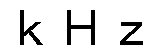 測定電圧を I V「 01 として測定し、 その平均値を求めた。 このとき、 試料 N 0. 7の積層セラ ミック電子部品の静電容量を基準値 (1. 〇〇) とし、 試料 N 0. 1〜 6の 積層セラミック電子部品の静電容量をその基準値に対する値に変換算出した
[0078] 次に、 各試料を !_ ハンダにてガラスエポキシ基板に実装した後、 一定の たわみ量 (5 ) で配線基板を 5秒間たわませた。 その後、 各試料に対し て、 1 25°〇、 相対湿度 95%[¾1~1、 1. 2気圧の高温高湿槽内にて、 定格 電圧を印加し、 1 〇〇〇時間の耐湿負荷加速試験を行った。 試験終了後、 各 試料についてシヨート状態であるサンプル数をカウントした。 ここで、 絶縁 抵抗値 (丨 値) が 2桁以上低下したものをシヨート状態であると判断した 。 中間電極がヒューズとして正常に機能した場合、 電極層間が一旦シヨート に至った後に、 中間電極が焼き切れ過電流が遮断される。 一方、 中間電極が ヒューズとして機能しなかった場合、 電極層間がシヨートした後、 絶縁復帰 せずにシヨート状態が維持される。
\¥0 2020/175169 18 卩(:170? 2020 /005687
[0079] その後、 試料 N 0 . 1〜 6については、 ヒューズ (中間電極) が焼き切れ たサンプル数をさらにカウントした。 カウントにあたっては、 試料 N 0 . 1 〜 6に研磨処理を施し中間電極を含む断面を露出させ、 ヒューズの状態を目 視した。 少なくとも 1つのヒューズが焼き切れているサンプルを、 ヒューズ が焼き切れたサンプルとしてカウントした。 以上の結果を表 1 に示す。
[0080] ◎
[表 1 ]

[0081 ] 表 1 に示すように、 中間電極を有する試料 1\!〇. 1〜 6では、 シヨート状 態のサンプルが発生しなかった。 これらの試料 1\1〇. 1〜 6はすべて、 中間 電極がカーボンナノチューブを約 2 0体積%以上含有していた。 さらに、 試 料 N 0 . 1〜 6はすべて、 セラミック層の主成分と、 中間電極が含有するセ ラミック材料の主成分とが同一組成 (已 3丁 丨 〇3) であった。
[0082] 電極層と中間電極との接合部が、 容量領域よりも外部電極側に位置してい る試料 N 0 . 5では、 電極層と中間電極との接合部が、 容量領域に位置して いる 1\1〇_ 1〜 4と比べて高い静電容量が得られた。
[0083] 中間電極が積層体の表面上のみに配置されている試料 1\!〇. 6では、 中間 電極が配置されていない試料 !\!〇. 7と比べても、 静電容量が低下していな
\¥02020/175169 19 卩(:170? 2020 /005687
かった。 これは、 試料 N 0. 6ではセラミック層、 電極層および中間電極を 同時に焼成する必要がないため、 セラミック層の高温での焼成が可能となる 。 そのため、 試料 N 0. 1〜 5と比べて密度のより高いセラミック層が得ら れたことに起因していると考えられる。
符号の説明
[0084] 1 00 積層セラミック電子部品
1 0 積層体
1 1 セラミック層
1 2 電極層
1 3 中間電極
1 4 エンドマージン領域
1 5 容量領域
Claims
[請求項 1 ] セラミック層と電極層とが交互に積層された積層体と、
該積層体の端部に設けられた 1対の外部電極と、 少なくとも 1つの前記電極層と一方の前記外部電極とを電気的に接 続している中間電極と、
を備え、
該中間電極が導電性炭素材料を含有している、 積層セラミック電子 部品。
[請求項 2] 前記中間電極が、 前記導電性炭素材料を 2 0体積%以上含有してい る、 請求項 1 に記載の積層セラミック電子部品。
[請求項 3] 前記中間電極における前記導電性炭素材料の含有率が、 5 0体積% 以下である、 請求項 1 または 2に記載の積層セラミック電子部品。
[請求項 4] 前記積層体が、 隣り合う前記電極層同士が対向する容量領域を備え 前記中間電極と前記電極層との接合部が、 前記容量領域よりも前記 外部電極側に位置している請求項 1〜 3のいずれかに記載の積層セラ ミック電子部品。
[請求項 5] 前記中間電極が、 前記積層体の表面上に存在する、 請求項 1〜 4の いずれかに記載の積層セラミック電子部品。
[請求項 6] 前記導電性炭素材料が、 導電性ポリマー、 力ーボンブラック、 力一 ボンナノチユーブ、 力ーボンナノファイバーまたはグラファイ トであ る、 請求項 1〜 5のいずれかに記載の積層コンデンサ。
Priority Applications (3)
| Application Number | Priority Date | Filing Date | Title |
|---|---|---|---|
| US17/427,942 US12136520B2 (en) | 2019-02-27 | 2020-02-14 | Laminated multilayer ceramic electronic component with alternating layers |
| CN202080013404.8A CN113424281B (zh) | 2019-02-27 | 2020-02-14 | 层叠陶瓷电子部件 |
| US18/904,829 US20250022657A1 (en) | 2019-02-27 | 2024-10-02 | Laminated ceramic electronic component |
Applications Claiming Priority (2)
| Application Number | Priority Date | Filing Date | Title |
|---|---|---|---|
| JP2019034411A JP7190937B2 (ja) | 2019-02-27 | 2019-02-27 | 積層セラミック電子部品 |
| JP2019-034411 | 2019-02-27 |
Related Child Applications (2)
| Application Number | Title | Priority Date | Filing Date |
|---|---|---|---|
| US17/427,942 A-371-Of-International US12136520B2 (en) | 2019-02-27 | 2020-02-14 | Laminated multilayer ceramic electronic component with alternating layers |
| US18/904,829 Continuation US20250022657A1 (en) | 2019-02-27 | 2024-10-02 | Laminated ceramic electronic component |
Publications (1)
| Publication Number | Publication Date |
|---|---|
| WO2020175169A1 true WO2020175169A1 (ja) | 2020-09-03 |
Family
ID=72238597
Family Applications (1)
| Application Number | Title | Priority Date | Filing Date |
|---|---|---|---|
| PCT/JP2020/005687 Ceased WO2020175169A1 (ja) | 2019-02-27 | 2020-02-14 | 積層セラミック電子部品 |
Country Status (4)
| Country | Link |
|---|---|
| US (2) | US12136520B2 (ja) |
| JP (1) | JP7190937B2 (ja) |
| CN (1) | CN113424281B (ja) |
| WO (1) | WO2020175169A1 (ja) |
Families Citing this family (3)
| Publication number | Priority date | Publication date | Assignee | Title |
|---|---|---|---|---|
| JP7264104B2 (ja) * | 2020-04-28 | 2023-04-25 | 株式会社村田製作所 | 積層型セラミック電子部品の製造方法および消失性インク |
| US12482606B2 (en) | 2023-05-23 | 2025-11-25 | Samsung Electro-Mechanics Co., Ltd. | Multilayered ceramic capacitor |
| JP2025139797A (ja) * | 2024-03-13 | 2025-09-29 | 株式会社村田製作所 | 積層セラミックコンデンサ |
Citations (4)
| Publication number | Priority date | Publication date | Assignee | Title |
|---|---|---|---|---|
| JPH02303109A (ja) * | 1989-05-18 | 1990-12-17 | Murata Mfg Co Ltd | ヒューズ機能付積層コンデンサ |
| JPH10284338A (ja) * | 1997-04-08 | 1998-10-23 | Murata Mfg Co Ltd | 積層セラミック電子部品およびその製造方法 |
| JP2002326868A (ja) * | 2001-05-01 | 2002-11-12 | Samsung Electro Mech Co Ltd | 誘電体磁器組成物及びそれを用いた磁器コンデンサ並びにそれらの製造方法 |
| JP2013040403A (ja) * | 2011-08-16 | 2013-02-28 | Samsung Electro-Mechanics Co Ltd | 金属粉末、その製造方法、及びその金属粉末からなる内部電極を含む積層セラミックキャパシタ |
Family Cites Families (26)
| Publication number | Priority date | Publication date | Assignee | Title |
|---|---|---|---|---|
| JPH09120930A (ja) * | 1995-10-24 | 1997-05-06 | Hitachi Aic Inc | 積層セラミックコンデンサ |
| JP4600082B2 (ja) * | 2005-02-24 | 2010-12-15 | 株式会社村田製作所 | 積層型複合電子部品 |
| KR101250669B1 (ko) * | 2010-11-16 | 2013-04-03 | 삼성전기주식회사 | 세라믹 전자부품 및 그 제조방법 |
| KR20130006783A (ko) * | 2011-06-23 | 2013-01-18 | 삼성전기주식회사 | 내부 전극용 도전성 페이스트 조성물 및 이를 포함하는 적층 세라믹 커패시터 |
| KR20130017984A (ko) * | 2011-08-12 | 2013-02-20 | 삼성전기주식회사 | 적층 세라믹 콘덴서 및 이의 제조방법 |
| KR20130017986A (ko) * | 2011-08-12 | 2013-02-20 | 삼성전기주식회사 | 내부 전극, 및 상기 내부 전극을 포함하는 적층형 세라믹 캐패시터 |
| KR101922864B1 (ko) * | 2011-08-23 | 2018-11-28 | 삼성전기 주식회사 | 적층 세라믹 전자 부품 및 이의 제조방법 |
| JP2013112536A (ja) * | 2011-11-25 | 2013-06-10 | Samsung Electro-Mechanics Co Ltd | 高誘電率セラミックスの製造方法 |
| KR101245347B1 (ko) * | 2011-12-29 | 2013-03-25 | 삼화콘덴서공업주식회사 | 적층 세라믹 커패시터 |
| KR101525652B1 (ko) * | 2012-05-04 | 2015-06-03 | 삼성전기주식회사 | 도전성 수지 조성물, 이를 포함하는 적층 세라믹 커패시터 및 그 제조방법 |
| JP5960816B2 (ja) * | 2012-06-21 | 2016-08-02 | 京セラ株式会社 | 積層セラミックコンデンサ |
| JP5567647B2 (ja) * | 2012-12-06 | 2014-08-06 | 太陽誘電株式会社 | セラミック電子部品 |
| KR102097329B1 (ko) * | 2013-09-12 | 2020-04-06 | 삼성전기주식회사 | 적층 세라믹 커패시터, 그 제조방법 및 적층 세라믹 커패시터 실장 기판 |
| JP6306316B2 (ja) | 2013-10-29 | 2018-04-04 | 京セラ株式会社 | コンデンサ |
| KR102007295B1 (ko) * | 2013-12-12 | 2019-08-05 | 삼성전기주식회사 | 적층 세라믹 커패시터, 그 제조방법 및 적층 세라믹 커패시터의 실장 기판 |
| KR101477430B1 (ko) * | 2013-12-30 | 2014-12-29 | 삼성전기주식회사 | 적층 세라믹 전자부품, 그 제조방법 및 적층 세라믹 전자부품의 실장 기판 |
| US10569330B2 (en) * | 2014-04-01 | 2020-02-25 | Forge Nano, Inc. | Energy storage devices having coated passive components |
| US10204737B2 (en) * | 2014-06-11 | 2019-02-12 | Avx Corporation | Low noise capacitors |
| US10102973B2 (en) * | 2014-09-12 | 2018-10-16 | Nanotek Instruments, Inc. | Graphene electrode based ceramic capacitor |
| WO2016121575A1 (ja) * | 2015-01-30 | 2016-08-04 | 株式会社村田製作所 | 電子部品の製造方法および電子部品 |
| KR102217287B1 (ko) * | 2015-05-19 | 2021-02-19 | 삼성전기주식회사 | 그래핀 내부전극 적층형 세라믹 콘덴서 및 그 제조방법 |
| KR102527715B1 (ko) * | 2016-11-21 | 2023-05-02 | 삼성전기주식회사 | 내부전극용 도전성 분말 및 커패시터 |
| US20200066457A1 (en) * | 2018-08-24 | 2020-02-27 | Apple Inc. | Self-fused capacitor |
| FR3091040B1 (fr) * | 2018-12-24 | 2022-12-09 | I Ten | Organe de contact d’un dispositif electronique ou electrochimique |
| CN111383844B (zh) * | 2018-12-26 | 2022-04-08 | 株式会社村田制作所 | 电解电容器 |
| KR102620527B1 (ko) * | 2019-01-21 | 2024-01-03 | 삼성전기주식회사 | 적층형 커패시터 및 그 제조 방법 |
-
2019
- 2019-02-27 JP JP2019034411A patent/JP7190937B2/ja active Active
-
2020
- 2020-02-14 WO PCT/JP2020/005687 patent/WO2020175169A1/ja not_active Ceased
- 2020-02-14 US US17/427,942 patent/US12136520B2/en active Active
- 2020-02-14 CN CN202080013404.8A patent/CN113424281B/zh active Active
-
2024
- 2024-10-02 US US18/904,829 patent/US20250022657A1/en active Pending
Patent Citations (4)
| Publication number | Priority date | Publication date | Assignee | Title |
|---|---|---|---|---|
| JPH02303109A (ja) * | 1989-05-18 | 1990-12-17 | Murata Mfg Co Ltd | ヒューズ機能付積層コンデンサ |
| JPH10284338A (ja) * | 1997-04-08 | 1998-10-23 | Murata Mfg Co Ltd | 積層セラミック電子部品およびその製造方法 |
| JP2002326868A (ja) * | 2001-05-01 | 2002-11-12 | Samsung Electro Mech Co Ltd | 誘電体磁器組成物及びそれを用いた磁器コンデンサ並びにそれらの製造方法 |
| JP2013040403A (ja) * | 2011-08-16 | 2013-02-28 | Samsung Electro-Mechanics Co Ltd | 金属粉末、その製造方法、及びその金属粉末からなる内部電極を含む積層セラミックキャパシタ |
Also Published As
| Publication number | Publication date |
|---|---|
| CN113424281B (zh) | 2022-11-08 |
| US12136520B2 (en) | 2024-11-05 |
| US20250022657A1 (en) | 2025-01-16 |
| US20220028617A1 (en) | 2022-01-27 |
| CN113424281A (zh) | 2021-09-21 |
| JP2020141016A (ja) | 2020-09-03 |
| JP7190937B2 (ja) | 2022-12-16 |
Similar Documents
| Publication | Publication Date | Title |
|---|---|---|
| US20250022657A1 (en) | Laminated ceramic electronic component | |
| CN108257779A (zh) | 层叠陶瓷电子部件 | |
| CN110310826B (zh) | 层叠陶瓷电子部件 | |
| CN110310825B (zh) | 层叠陶瓷电子部件 | |
| CN110310830B (zh) | 层叠陶瓷电子部件 | |
| CN110310828B (zh) | 层叠陶瓷电子部件 | |
| US20060138590A1 (en) | Electronic parts and method for manufacture thereof | |
| JP5870625B2 (ja) | 電極焼結体、積層電子部品、内部電極ペースト、電極焼結体の製造方法、積層電子部品の製造方法 | |
| CN103270656B (zh) | Esd保护装置及其制造方法 | |
| JP5423977B2 (ja) | 積層セラミック電子部品の製造方法 | |
| JP7290431B2 (ja) | 積層セラミック電子部品 | |
| CN112750622A (zh) | 导电性膏以及层叠型电子部件 | |
| JP5887919B2 (ja) | 電極焼結体および積層電子部品 | |
| JP5998785B2 (ja) | 積層電子部品 | |
| JP4905569B2 (ja) | 導電性ペースト、積層セラミック電子部品及びその製造方法 | |
| WO2020158461A1 (ja) | 積層セラミックコンデンサ | |
| JP2007234330A (ja) | 導電体ペーストおよび電子部品 | |
| JP4076393B2 (ja) | 導電性ペーストおよび電子部品 | |
| JP2013135096A (ja) | 電極焼結体、積層電子部品、内部電極ペースト、電極焼結体の製造方法、積層電子部品の製造方法 | |
| JP5899912B2 (ja) | 電極焼結体、積層電子部品、内部電極ペースト、電極焼結体の製造方法、積層電子部品の製造方法 | |
| JP2003068565A (ja) | 積層セラミック電子部品の製造方法および積層セラミック電子部品 | |
| JP4432895B2 (ja) | 導電性ペースト、積層セラミック電子部品及びその製造方法 | |
| JP2007081339A (ja) | 導電性ペースト、積層セラミック電子部品及びその製造方法 | |
| JP2002270454A (ja) | 積層セラミックコンデンサおよびその製法 | |
| JP3502745B2 (ja) | 内部電極ペーストおよび積層セラミックコンデンサ |
Legal Events
| Date | Code | Title | Description |
|---|---|---|---|
| 121 | Ep: the epo has been informed by wipo that ep was designated in this application |
Ref document number: 20762804 Country of ref document: EP Kind code of ref document: A1 |
|
| NENP | Non-entry into the national phase |
Ref country code: DE |
|
| 122 | Ep: pct application non-entry in european phase |
Ref document number: 20762804 Country of ref document: EP Kind code of ref document: A1 |