WO2020170949A1 - 酸化物焼結体、スパッタリングターゲット及びスパッタリングターゲットの製造方法 - Google Patents
酸化物焼結体、スパッタリングターゲット及びスパッタリングターゲットの製造方法 Download PDFInfo
- Publication number
- WO2020170949A1 WO2020170949A1 PCT/JP2020/005666 JP2020005666W WO2020170949A1 WO 2020170949 A1 WO2020170949 A1 WO 2020170949A1 JP 2020005666 W JP2020005666 W JP 2020005666W WO 2020170949 A1 WO2020170949 A1 WO 2020170949A1
- Authority
- WO
- WIPO (PCT)
- Prior art keywords
- sintered body
- oxide sintered
- sputtering target
- raw material
- less
- Prior art date
- Legal status (The legal status is an assumption and is not a legal conclusion. Google has not performed a legal analysis and makes no representation as to the accuracy of the status listed.)
- Ceased
Links
Images





Classifications
-
- C—CHEMISTRY; METALLURGY
- C04—CEMENTS; CONCRETE; ARTIFICIAL STONE; CERAMICS; REFRACTORIES
- C04B—LIME, MAGNESIA; SLAG; CEMENTS; COMPOSITIONS THEREOF, e.g. MORTARS, CONCRETE OR LIKE BUILDING MATERIALS; ARTIFICIAL STONE; CERAMICS; REFRACTORIES; TREATMENT OF NATURAL STONE
- C04B35/00—Shaped ceramic products characterised by their composition; Ceramics compositions; Processing powders of inorganic compounds preparatory to the manufacturing of ceramic products
- C04B35/01—Shaped ceramic products characterised by their composition; Ceramics compositions; Processing powders of inorganic compounds preparatory to the manufacturing of ceramic products based on oxide ceramics
- C04B35/453—Shaped ceramic products characterised by their composition; Ceramics compositions; Processing powders of inorganic compounds preparatory to the manufacturing of ceramic products based on oxide ceramics based on zinc, tin, or bismuth oxides or solid solutions thereof with other oxides, e.g. zincates, stannates or bismuthates
-
- C—CHEMISTRY; METALLURGY
- C04—CEMENTS; CONCRETE; ARTIFICIAL STONE; CERAMICS; REFRACTORIES
- C04B—LIME, MAGNESIA; SLAG; CEMENTS; COMPOSITIONS THEREOF, e.g. MORTARS, CONCRETE OR LIKE BUILDING MATERIALS; ARTIFICIAL STONE; CERAMICS; REFRACTORIES; TREATMENT OF NATURAL STONE
- C04B35/00—Shaped ceramic products characterised by their composition; Ceramics compositions; Processing powders of inorganic compounds preparatory to the manufacturing of ceramic products
- C04B35/622—Forming processes; Processing powders of inorganic compounds preparatory to the manufacturing of ceramic products
- C04B35/626—Preparing or treating the powders individually or as batches ; preparing or treating macroscopic reinforcing agents for ceramic products, e.g. fibres; mechanical aspects section B
- C04B35/62605—Treating the starting powders individually or as mixtures
- C04B35/62695—Granulation or pelletising
-
- C—CHEMISTRY; METALLURGY
- C04—CEMENTS; CONCRETE; ARTIFICIAL STONE; CERAMICS; REFRACTORIES
- C04B—LIME, MAGNESIA; SLAG; CEMENTS; COMPOSITIONS THEREOF, e.g. MORTARS, CONCRETE OR LIKE BUILDING MATERIALS; ARTIFICIAL STONE; CERAMICS; REFRACTORIES; TREATMENT OF NATURAL STONE
- C04B35/00—Shaped ceramic products characterised by their composition; Ceramics compositions; Processing powders of inorganic compounds preparatory to the manufacturing of ceramic products
- C04B35/622—Forming processes; Processing powders of inorganic compounds preparatory to the manufacturing of ceramic products
- C04B35/64—Burning or sintering processes
-
- C—CHEMISTRY; METALLURGY
- C23—COATING METALLIC MATERIAL; COATING MATERIAL WITH METALLIC MATERIAL; CHEMICAL SURFACE TREATMENT; DIFFUSION TREATMENT OF METALLIC MATERIAL; COATING BY VACUUM EVAPORATION, BY SPUTTERING, BY ION IMPLANTATION OR BY CHEMICAL VAPOUR DEPOSITION, IN GENERAL; INHIBITING CORROSION OF METALLIC MATERIAL OR INCRUSTATION IN GENERAL
- C23C—COATING METALLIC MATERIAL; COATING MATERIAL WITH METALLIC MATERIAL; SURFACE TREATMENT OF METALLIC MATERIAL BY DIFFUSION INTO THE SURFACE, BY CHEMICAL CONVERSION OR SUBSTITUTION; COATING BY VACUUM EVAPORATION, BY SPUTTERING, BY ION IMPLANTATION OR BY CHEMICAL VAPOUR DEPOSITION, IN GENERAL
- C23C14/00—Coating by vacuum evaporation, by sputtering or by ion implantation of the coating forming material
- C23C14/22—Coating by vacuum evaporation, by sputtering or by ion implantation of the coating forming material characterised by the process of coating
- C23C14/34—Sputtering
-
- C—CHEMISTRY; METALLURGY
- C23—COATING METALLIC MATERIAL; COATING MATERIAL WITH METALLIC MATERIAL; CHEMICAL SURFACE TREATMENT; DIFFUSION TREATMENT OF METALLIC MATERIAL; COATING BY VACUUM EVAPORATION, BY SPUTTERING, BY ION IMPLANTATION OR BY CHEMICAL VAPOUR DEPOSITION, IN GENERAL; INHIBITING CORROSION OF METALLIC MATERIAL OR INCRUSTATION IN GENERAL
- C23C—COATING METALLIC MATERIAL; COATING MATERIAL WITH METALLIC MATERIAL; SURFACE TREATMENT OF METALLIC MATERIAL BY DIFFUSION INTO THE SURFACE, BY CHEMICAL CONVERSION OR SUBSTITUTION; COATING BY VACUUM EVAPORATION, BY SPUTTERING, BY ION IMPLANTATION OR BY CHEMICAL VAPOUR DEPOSITION, IN GENERAL
- C23C14/00—Coating by vacuum evaporation, by sputtering or by ion implantation of the coating forming material
- C23C14/22—Coating by vacuum evaporation, by sputtering or by ion implantation of the coating forming material characterised by the process of coating
- C23C14/34—Sputtering
- C23C14/3407—Cathode assembly for sputtering apparatus, e.g. Target
-
- C—CHEMISTRY; METALLURGY
- C04—CEMENTS; CONCRETE; ARTIFICIAL STONE; CERAMICS; REFRACTORIES
- C04B—LIME, MAGNESIA; SLAG; CEMENTS; COMPOSITIONS THEREOF, e.g. MORTARS, CONCRETE OR LIKE BUILDING MATERIALS; ARTIFICIAL STONE; CERAMICS; REFRACTORIES; TREATMENT OF NATURAL STONE
- C04B2235/00—Aspects relating to ceramic starting mixtures or sintered ceramic products
- C04B2235/02—Composition of constituents of the starting material or of secondary phases of the final product
- C04B2235/50—Constituents or additives of the starting mixture chosen for their shape or used because of their shape or their physical appearance
- C04B2235/54—Particle size related information
- C04B2235/5418—Particle size related information expressed by the size of the particles or aggregates thereof
- C04B2235/5436—Particle size related information expressed by the size of the particles or aggregates thereof micrometer sized, i.e. from 1 to 100 micron
-
- C—CHEMISTRY; METALLURGY
- C04—CEMENTS; CONCRETE; ARTIFICIAL STONE; CERAMICS; REFRACTORIES
- C04B—LIME, MAGNESIA; SLAG; CEMENTS; COMPOSITIONS THEREOF, e.g. MORTARS, CONCRETE OR LIKE BUILDING MATERIALS; ARTIFICIAL STONE; CERAMICS; REFRACTORIES; TREATMENT OF NATURAL STONE
- C04B2235/00—Aspects relating to ceramic starting mixtures or sintered ceramic products
- C04B2235/70—Aspects relating to sintered or melt-casted ceramic products
- C04B2235/96—Properties of ceramic products, e.g. mechanical properties such as strength, toughness, wear resistance
Definitions
- the present invention relates to an oxide sintered body, a sputtering target, and a method for manufacturing a sputtering target.
- TFT thin film transistor
- oxide semiconductors have been attracting attention as a material used for a channel layer of a TFT with a demand for higher definition of a display.
- an amorphous oxide semiconductor containing indium, gallium, zinc, and oxygen (In—Ga—Zn—O, abbreviated as “IGZO” hereinafter) has high carrier mobility and thus is preferable. It is used.
- IGZO has a drawback that the raw material cost is high because In and Ga are used as raw materials.
- ZTO Zn—Sn—O
- ITZO In—Sn—Zn—O in which Sn is added instead of Ga of IGZO
- ITZO has a large thermal expansion coefficient and a low thermal conductivity
- cracks are likely to occur due to thermal stress during bonding to a backing plate such as Cu or Ti and during sputtering.
- reliability which is the greatest problem of oxide semiconductor materials, can be improved by densifying the film.
- High power film formation is effective for densifying the film.
- cracking of the end portion of the target on which plasma is concentrated poses a problem, and particularly the ITZO-based material target tends to crack easily.
- Non-Patent Document 1 describes that in ceramics, Vickers hardness and tensile strength are in a proportional relationship.
- Patent Document 1 zinc oxide, tin oxide, and an oxide of at least one metal (M metal) selected from the group consisting of Al, Hf, Ni, Si, Ga, In, and Ta are mixed. And an oxide sintered body obtained by sintering, which has a Vickers hardness of 400 Hv or more. Patent Document 1 describes that nodule is unlikely to occur even when a film is formed by using a DC sputtering method using such an oxide sintered body, and stable discharge is possible for a long time. ..
- M metal metal
- Patent Document 1 describes that the Vickers hardness of a sputtering target containing an oxide sintered body is defined within a predetermined range, the Vickers hardness in Patent Document 1 shows that the oxide sintered body is t/2. It is a value obtained by measuring the position of the surface of the cut surface cut at (t: thickness). Therefore, Patent Document 1 does not describe the Vickers hardness on the surface of the oxide sintered body. In recent years, there has been a demand for a target having improved crack resistance during sputtering, but Patent Document 1 describes that the generation of nodules is suppressed by controlling the hardness of the oxide sintered body. However, it does not describe a method for improving crack resistance. Further, although Patent Document 1 describes that the sintering conditions and the subsequent heat treatment conditions are appropriately controlled in order to control the hardness of the oxide sintered body, the conditions described in Patent Document 1 do not apply. , It is difficult to improve crack resistance.
- An object of the present invention is to provide an oxide sintered body and a sputtering target having improved crack resistance, and a method for manufacturing the sputtering target.
- An oxide sintered body wherein the average value of the Vickers hardness of the surface of the oxide sintered body is more than 500 Hv and less than 900 Hv.
- the oxide sintered body further contains an X element, and the X element is a germanium element, a silicon element, a yttrium element, a zirconium element, an aluminum element, a magnesium element, a ytterbium element, and A sputtering target, which is at least one element selected from the group consisting of gallium elements.
- a method for manufacturing a sputtering target for manufacturing the sputtering target according to any one of [1] to [5], [2A] and [5A], A step of granulating the raw material of the oxide sintered body to obtain a raw material granulated powder having a particle size of 25 ⁇ m or more and 150 ⁇ m or less;
- an oxide sintered body and a sputtering target with improved crack resistance can be provided.
- a method of manufacturing a sputtering target according to one aspect of the present invention can be provided.
- the crack of the sputtering target is generated from a weak portion of the target as a starting point. Therefore, the inventor of the present invention has considered reducing the variation in strength in the plane of the sputtering target, particularly improving the minimum strength, as a measure for improving the crack resistance.
- the present inventor as a result of diligent examination of the manufacturing conditions of the sputtering target, by optimizing the particle size of the raw material granulated powder and the sintering temperature, the minimum value of the Vickers hardness on the sputtering surface of the oxide sintered body is improved. However, it was found that the average value is improved.
- the average value of the Vickers hardness in the oxide sintered body has an optimum range, and if the Vickers hardness is too high, microcracks are generated in the target grinding step, and the crack resistance is reduced.
- the present inventor invented the present invention based on these findings.
- film or “thin film” and “layer” can be interchanged with each other in some cases.
- the term “compound” and the term “crystalline phase” can be interchanged with each other in some cases.
- the "oxide sintered body” may be simply referred to as “sintered body”.
- the “sputtering target” may be simply referred to as “target”.
- a sputtering target according to one embodiment of the present invention (hereinafter, may be simply referred to as a sputtering target according to this embodiment) includes an oxide sintered body.
- the sputtering target according to the present embodiment is obtained, for example, by cutting and polishing a bulk of an oxide sintered body into a shape suitable as a sputtering target.
- the sputtering target according to the present embodiment can also be obtained by bonding a sputtering target material obtained by grinding and polishing a bulk of an oxide sintered body to a backing plate.
- a target made of only an oxide sintered body is also included.
- the shape of the oxide sintered body is not particularly limited.
- a plate-shaped oxide sintered body as indicated by reference numeral 1 in FIG. 1 may be used.
- a cylindrical oxide sintered body as indicated by reference numeral 1A in FIG. 2 may be used.
- the planar shape of the oxide sintered body may be rectangular as shown by reference numeral 1 in FIG. 1 or circular as shown by reference numeral 1B in FIG.
- the oxide sintered body may be an integrally molded product, or may be divided into a plurality of pieces as shown in FIG.
- Each of the plurality of divided oxide sintered bodies (reference numeral 1C) may be fixed to the backing plate 3.
- the sputtering target obtained by bonding the plurality of oxide sintered bodies 1C to one backing plate 3 as described above may be referred to as a multi-split sputtering target.
- the backing plate 3 is a member for holding and cooling the oxide sintered body.
- the material of the backing plate 3 is not particularly limited. As the material of the backing plate 3, for example, at least one material selected from the group consisting of Cu, Ti, SUS and the like is used.
- the average value (H av ) of Vickers hardness on the surface of the oxide sintered body is more than 500 Hv and less than 900 Hv.
- the Vickers hardness is measured according to JIS Z 2244:2009 using a Hardness Tester (AKASHI MVK-E3). For the measurement points, data was collected every 30 mm from one end along the center line of the oxide sintered body (142 x 305 mm size), and the average value of the collected data was Vickers on the surface of the oxide sintered body. The average hardness (H av ) is used.
- the average value (H av ) of Vickers hardness on the surface of the oxide sintered body exceeds 500 Hv, there are few weak portions on the sputtering surface of the target. Therefore, the crack resistance of the sputtering target according to the present embodiment is improved. If the Vickers hardness is too high, microcracks may occur during the grinding process. However, in the present embodiment, since the average value (H av ) of the Vickers hardness of the surface of the oxide sintered body is less than 900 Hv, it is possible to suppress the generation of microcracks in the target grinding step. As a result, it is possible to suppress a decrease in crack resistance caused by microcracks.
- the average value (H av ) of Vickers hardness on the surface of the oxide sintered body is preferably 520 Hv or more and 850 Hv or less, and more preferably 600 Hv or more and 750 Hv or less.
- the minimum value (H min ) of Vickers hardness on the surface of the oxide sintered body is preferably more than 500 Hv, more preferably 600 Hv or more.
- the minimum value (H min ) of Vickers hardness exceeds 500 Hv, there are fewer weak portions on the sputtering surface of the target, and crack resistance is further improved.
- the minimum value (H min ) of Vickers hardness is the lowest value among the values of Vickers hardness measured at 10 points on the surface of the oxide sintered body. is there.
- the maximum Vickers hardness (H max ) on the surface of the oxide sintered body is preferably less than 900 Hv, and more preferably 850 Hv or less.
- the minimum value (H max ) of Vickers hardness is less than 900 Hv, generation of microcracks in the target grinding process is further suppressed, and as a result, crack resistance is further improved.
- the maximum value ( Hmax ) of Vickers hardness is the largest value among the values of the Vickers hardness of the 10 locations measured by measuring the Vickers hardness at 10 locations on the surface of the oxide sintered body. is there.
- the oxide sintered body according to the present embodiment preferably contains indium element (In), tin element (Sn), and zinc element (Zn).
- the oxide sintered body according to the present embodiment may contain a metal element other than In, Sn, and Zn within a range that does not impair the effects of the present invention, and substantially contains In, Sn, and Zn. It may be contained only or may be composed only of In, Sn and Zn.
- substantially means that 95% by mass or more and 100% by mass or less (preferably 98% by mass or more and 100% by mass or less) of the metal element of the oxide sintered body is indium element (In) or tin element (Sn).
- zinc element (Zn) zinc element
- the oxide sintered body according to the present embodiment may contain inevitable impurities in addition to In, Sn, Zn, and oxygen element (O) as long as the effects of the present invention are not impaired.
- the unavoidable impurities here mean elements that are not intentionally added and that are mixed in the raw material or the manufacturing process.
- the oxide sintered body according to the present embodiment also preferably contains an indium element (In), a tin element (Sn), a zinc element (Zn), and an X element.
- the oxide sintered body according to the present embodiment may contain a metal element other than In, Sn, Zn, and the X element as long as the effect of the present invention is not impaired, or substantially In, It may contain only Sn, Zn and X elements, or may consist only of In, Sn, Zn and X elements.
- “substantially” means In, Sn, Zn and X elements in which 95% by mass or more and 100% by mass or less (preferably 98% by mass or more and 100% by mass or less) of the metal elements of the oxide sintered body are used. Means that.
- the oxide sintered body according to the present embodiment may contain inevitable impurities in addition to In, Sn, Zn, the X element, and the oxygen element (O) as long as the effects of the present invention are not impaired.
- the unavoidable impurities here mean elements that are not intentionally added and that are mixed in the raw material or the manufacturing process.
- the X element is germanium element (Ge), silicon element (Si), yttrium element (Y), zirconium element (Zr), aluminum element (Al), magnesium element (Mg), ytterbium element (Yb) and gallium element (Ga).
- unavoidable impurities include alkali metals (Li, Na, K, Rb, etc.), alkaline earth metals (Ca, Sr, Ba, etc.), hydrogen (H) element, boron (B) element, carbon (C). It is an element, a nitrogen (N) element, a fluorine (F) element, and a chlorine (Cl) element.
- the impurity concentration can be measured by ICP or SIMS.
- the impurity concentration (H, C, N, F, Si, Cl) in the obtained sintered body was analyzed by SIMS using a sector type dynamic secondary ion mass spectrometer (IMS 7f-Auto, manufactured by AMETEK CAMECA). Can be evaluated quantitatively. Specifically, first, using primary ions Cs + , sputtering is performed at a accelerating voltage of 14.5 kV to a depth of 20 ⁇ m from the surface of the sintered body to be measured.
- each impurity is injected into the sintered body by controlling the dose amount by ion implantation to prepare a standard sample having a known impurity concentration.
- the mass spectrum intensity of impurities H, C, N, F, Si, Cl
- the relational expression between the absolute value of the impurity concentration and the mass spectrum intensity is used as a calibration curve.
- the mass spectrum intensity of the sintered body to be measured and the calibration curve are used to calculate the impurity concentration of the measured object, and this is used as the absolute value of the impurity concentration (atom ⁇ cm ⁇ 3 ).
- the impurity concentration (B, Na) of the obtained sintered body can also be quantitatively evaluated by SIMS analysis using a sector type dynamic secondary ion mass spectrometer (IMS 7f-Auto, manufactured by AMETEK CAMECA). Measured by the same evaluation as H, C, N, F, Si, Cl except that the primary ion is O 2 + , the accelerating voltage of the primary ion is 5.5 kV, and the mass spectrum of each impurity is measured. The absolute value (atom ⁇ cm ⁇ 3 ) of the target impurity concentration can be obtained.
- the atomic composition ratio of each element satisfies at least one of the following formulas (1) to (3). 0.40 ⁇ Zn/(In+Sn+Zn) ⁇ 0.80 (1) 0.15 ⁇ Sn/(Sn+Zn) ⁇ 0.40 (2) 0.10 ⁇ In/(In+Sn+Zn) ⁇ 0.35 (3)
- Zn and Sn represent the contents of indium element, zinc element and tin element in the oxide sintered body, respectively.
- Zn/(In+Sn+Zn) When Zn/(In+Sn+Zn) is 0.40 or more, a spinel phase is easily generated in the oxide sintered body, and semiconductor characteristics can be easily obtained. When Zn/(In+Sn+Zn) is 0.80 or less, it is possible to suppress a decrease in strength due to abnormal grain growth of the spinel phase in the oxide sintered body. When Zn/(In+Sn+Zn) is 0.80 or less, a decrease in mobility of the oxide semiconductor thin film can be suppressed. Zn/(In+Sn+Zn) is more preferably 0.50 or more and 0.70 or less.
- Sn/(Sn+Zn) When Sn/(Sn+Zn) is 0.15 or more, it is possible to suppress a decrease in strength due to abnormal grain growth of the spinel phase in the oxide sintered body.
- Sn/(Sn+Zn) When Sn/(Sn+Zn) is 0.40 or less, aggregation of tin oxide, which causes abnormal discharge during sputtering, can be suppressed in the oxide sintered body.
- Sn/(Sn+Zn) When Sn/(Sn+Zn) is 0.40 or less, the oxide semiconductor thin film formed by using the sputtering target can be easily etched by a weak acid such as oxalic acid.
- Sn/(Sn+Zn) When Sn/(Sn+Zn) is 0.15 or more, it is possible to prevent the etching rate from becoming too fast, which facilitates the control of etching.
- Sn/(Sn+Zn) is more preferably 0.15 or more and
- In/(In+Sn+Zn) is 0.10 or more, the bulk resistance of the obtained sputtering target can be lowered.
- In/(In+Sn+Zn) is 0.10 or more, the mobility of the oxide semiconductor thin film can be prevented from being extremely low.
- In/(In+Sn+Zn) is 0.35 or less, it is possible to prevent the film from becoming a conductor during sputtering film formation, and it becomes easy to obtain characteristics as a semiconductor.
- In/(In+Sn+Zn) is preferably 0.10 or more and 0.30 or less.
- the oxide sintered body according to the present embodiment contains the X element
- the atomic ratio of each element preferably satisfies the following formula (1X). 0.001 ⁇ X/(In+Sn+Zn+X) ⁇ 0.05 (1X)
- In, Zn, Sn, and X represent the contents of indium element, zinc element, tin element, and X element, respectively, in the oxide sintered body.
- the crack resistance of the oxide sintered body according to this embodiment can be sufficiently increased.
- the X element is preferably at least one selected from the group consisting of silicon element (Si), aluminum element (Al), magnesium element (Mg), ytterbium element (Yb), and gallium element (Ga). More preferably, the X element is at least one selected from the group consisting of a silicon element (Si), an aluminum element (Al) and a gallium element (Ga). Aluminum element (Al) and gallium element (Ga) are more preferable because the composition of the oxide as a raw material is stable and the effect of improving crack resistance is high.
- the strength reduction of the sputtering target can be suppressed.
- X/(In+Sn+Zn+X) is 0.05 or less, the oxide semiconductor thin film formed by using the sputtering target including the oxide sintered body can be easily etched by a weak acid such as oxalic acid. become.
- X/(In+Sn+Zn+X) is 0.05 or less, it is possible to suppress a decrease in TFT characteristics, particularly mobility.
- X/(In+Sn+Zn+X) is preferably 0.001 or more and 0.05 or less, more preferably 0.003 or more and 0.03 or less, and 0.005 or more and 0.01 or less. Is more preferable and 0.005 or more and less than 0.01 is even more preferable.
- the oxide sintered body according to the present embodiment contains the X element, the X element may be only one kind or two or more kinds. When two or more X elements are contained, X in the formula (1X) is the total atomic ratio of X elements.
- the existing form of the X element in the oxide sintered body is not particularly specified. Examples of the existence form of the X element in the oxide sintered body include a form existing as an oxide, a form in which it is in solid solution, and a form segregated at grain boundaries.
- the atomic ratio of each metal element of the oxide sintered body can be controlled by the blending amount of the raw materials. Further, the atomic ratio of each element can be obtained by quantitatively analyzing the contained element with an inductively coupled plasma emission spectroscopic analyzer (ICP-AES).
- ICP-AES inductively coupled plasma emission spectroscopic analyzer
- the oxide sintered body according to the present embodiment preferably contains a spinel structure compound represented by Zn 2-x Sn 1-y In x+y O 4 [0 ⁇ x ⁇ 2, 0 ⁇ y ⁇ 1]. ..
- a spinel structure compound may be referred to as a spinel compound.
- Zn 2-x Sn 1-y In x+y O 4 when x is 0 and y is 0, it is represented by Zn 2 SnO 4 .
- the oxide sintered body according to the present embodiment preferably contains a hexagonal layered compound represented by In 2 O 3 (ZnO) m .
- m is an integer of 2 to 7, and preferably an integer of 3 to 5.
- m is 2 or more, the compound has a hexagonal layered structure.
- m is 7 or less, the bulk resistance of the oxide sintered body is low.
- the hexagonal layered compound composed of indium oxide and zinc oxide is a compound showing an X-ray diffraction pattern belonging to the hexagonal layered compound, when measured by an X-ray diffraction method.
- the hexagonal layered compound contained in the oxide sintered body is a compound represented by In 2 O 3 (ZnO) m .
- the oxide sintered body according to the present embodiment is composed of Zn 2 ⁇ x Sn 1 ⁇ y In x+y O 4 [0 ⁇ x ⁇ 2, 0 ⁇ y ⁇ 1] and a spinel structure compound and In 2 O 3 .
- the represented bixbyite structure compound may be contained.
- the bulk resistance of the sputtering target can be made sufficiently low as long as the content ratio of the X element is within the range of the above formula (1X).
- the bulk resistance of the sputtering target according to the present embodiment is preferably 50 m ⁇ cm or less, more preferably 25 m ⁇ cm or less, further preferably 10 m ⁇ cm or less, further preferably 5 m ⁇ cm or less, and 3 m ⁇ cm or less. Is particularly preferable. If the bulk resistance is 50 m ⁇ cm or less, stable film formation can be performed by DC sputtering.
- the bulk resistance value can be measured based on the four-point probe method (JIS R 1637:1998) using a known resistivity meter. The number of measurement points is about 9, and it is preferable to use the average value of the measured values of 9 points as the bulk resistance value.
- the measurement points are preferably divided into 3 ⁇ 3 9 parts, and the center points of the respective quadrangles are preferably 9 points.
- the planar shape of the oxide sintered body is circular, it is preferable that the square inscribed in the circle is divided into 3 ⁇ 3 9 parts, and the central points of the respective squares are 9 points.
- the average crystal grain size of the oxide sintered body according to the present embodiment is preferably 10 ⁇ m or less, and more preferably 8 ⁇ m or less from the viewpoint of preventing abnormal discharge and easiness of production. When the average crystal grain size is 10 ⁇ m or less, abnormal discharge caused by grain boundaries can be prevented.
- the lower limit of the average crystal grain size of the oxide sintered body is not particularly limited, but is preferably 1 ⁇ m or more from the viewpoint of ease of production.
- the average crystal grain size can be adjusted by selecting raw materials and changing manufacturing conditions. Specifically, it is preferable to use a raw material having a small average particle diameter, and it is more preferable to use a raw material having an average particle diameter of 1 ⁇ m or less. Further, during sintering, the higher the sintering temperature or the longer the sintering time, the larger the average crystal grain size tends to be.
- the average crystal grain size can be measured as follows. When the surface of the oxide sintered body is polished and the plane shape is a quadrangle, the surface is divided into 16 equal areas, and at the center point of each quadrangle, the magnification is 1000 times (80 ⁇ m ⁇ 125 ⁇ m) in a frame. The average particle size of the particles in the frame at 16 points is determined, and finally the average value of the measured values at 16 points is taken as the average crystal grain size. When the surface of the oxide sintered body is polished and the plane shape is circular, the square inscribed in the circle is divided into 16 equal areas, and the magnification is 1000 times (80 ⁇ m ⁇ 125 ⁇ m) at 16 central points of each square.
- the particle size of the particles observed in the frame is measured, and the average value of the particle sizes of the particles in the 16 frames is determined.
- the particle size of the crystal grain is measured as the equivalent circle diameter based on JIS R 1670:2006.
- a circle ruler is applied to the measurement target grain in the microstructure photograph, and the diameter corresponding to the area of the target grain is read.
- the average value of the longest diameter and the shortest diameter is taken as the particle diameter of the particle.
- the crystal grains can be observed with a scanning electron microscope (SEM).
- SEM scanning electron microscope
- the difference between the average crystal grain size of the hexagonal layered compound and the average crystal grain size of the spinel compound is 1 ⁇ m or less.
- the strength of the oxide sintered body can be improved. More preferably, the average crystal grain size of the oxide sintered body according to the present embodiment is 10 ⁇ m or less, and the difference between the average crystal grain size of the hexagonal layered compound and the average crystal grain size of the spinel compound is 1 ⁇ m or less. ..
- the oxide sintered body according to the present embodiment contains a bixbyite structure compound and a spinel compound
- the difference between the average crystal grain size of the bixbite structure compound and the average crystal grain size of the spinel compound is 1 ⁇ m.
- the following is preferable.
- the oxide sintered body according to the present embodiment has an average crystal grain size of 10 ⁇ m or less, and a difference between the average crystal grain size of the bixbyite structure compound and the spinel compound is 1 ⁇ m or less. ..
- the relative density of the oxide sintered body according to this embodiment is preferably 95% or more, and more preferably 96% or more.
- the sputtering target according to the present embodiment has high mechanical strength and excellent conductivity. Therefore, when the sputtering target according to the present embodiment is attached to the RF magnetron sputtering apparatus or the DC magnetron sputtering apparatus to perform sputtering, the stability of plasma discharge can be further enhanced.
- the relative density of the oxide sintered body is calculated from the inherent density of each oxide in the sintered body and the composition ratio thereof, and shows the actually measured density of the oxide sintered body with respect to the theoretical density, as a percentage.
- the relative density of the oxide sintered body is, for example, a theoretical density calculated from the inherent densities of indium oxide, zinc oxide and tin oxide, and the respective oxides of the X element contained as necessary, and their composition ratios. Is the actual measured density of the oxide sintered body with respect to the above as a percentage.
- the relative density of the oxide sintered body can be measured based on the Archimedes method.
- Equation 5 C 1 to C n respectively represent the content (mass %) of the oxide sintered body or the constituent material of the oxide sintered body, and ⁇ 1 to ⁇ n are The densities (g/cm 3 ) of the constituent substances corresponding to C 1 to C n are shown. Since the density is almost the same as the specific gravity, the density of each constituent substance uses the value of the specific gravity of the oxide described in the Chemical Handbook, Basic Edition, I Chemical Society of Japan, Revised 2nd Edition (Maruzen Co., Ltd.). be able to.
- the method for producing an oxide sintered body includes a mixing/pulverizing step, a granulating step, a forming step, and a sintering step.
- the method for producing an oxide sintered body may include other steps.
- An annealing process is mentioned as another process.
- each step will be specifically described by taking the case of producing an ITZO-based oxide sintered body as an example.
- the oxide sintered body according to the present embodiment is a mixing/pulverizing step of mixing and pulverizing an indium raw material, a zinc raw material, a tin raw material, and an X element raw material, a granulating step of granulating a raw material mixture, a molding step of molding, and a molding. It can be manufactured through a sintering step of sintering an object and an annealing step of annealing a sintered body as necessary.
- the mixing/crushing step is a step of mixing and crushing the raw materials of the oxide sintered body to obtain a raw material mixture.
- the raw material mixture is preferably in powder form, for example.
- the mixing/pulverizing step first, raw materials for the oxide sintered body are prepared.
- the raw materials for producing the oxide sintered body containing In, Zn and Sn are as follows.
- the indium raw material (In raw material) is not particularly limited as long as it is a compound or metal containing In.
- the zinc raw material (Zn raw material) is not particularly limited as long as it is a compound or metal containing Zn.
- the tin raw material (Sn raw material) is not particularly limited as long as it is a compound or metal containing Sn.
- the raw materials for producing the oxide sintered body containing the element X are as follows.
- the raw material of the X element is not particularly limited as long as it is a compound or a metal containing the X element.
- the In raw material, the Zn raw material, the Sn raw material, and the raw material of the X element are preferably oxides.
- Raw materials such as indium oxide, zinc oxide, tin oxide, and X element oxide are preferably highly pure.
- the purity of the raw material of the oxide sintered body is preferably 99% by mass or more, more preferably 99.9% by mass or more, and further preferably 99.99% by mass or more.
- a high-purity raw material is used, a sintered body having a dense structure is obtained, and the volume resistivity of the sputtering target made of the sintered body becomes low.
- the average particle size of the primary particles of the metal oxide as a raw material is preferably 0.01 ⁇ m or more and 10 ⁇ m or less, more preferably 0.05 ⁇ m or more and 5 ⁇ m or less, and 0.1 ⁇ m or more and 5 ⁇ m or less. Is more preferable. If the average particle size of the primary particles of the metal oxide as a raw material is 0.01 ⁇ m or more, aggregation is less likely to occur, and if the average particle size is 10 ⁇ m or less, the mixing property is sufficient and a sintered body having a dense structure is obtained. Is obtained.
- the average particle diameter is measured by a laser diffraction type particle size distribution measuring device SALD-300V (manufactured by Shimadzu Corporation) using a median diameter D50.
- the raw material of the oxide sintered body is mixed and pulverized with a bead mill, etc., by adding a dispersant for releasing the agglomeration and a thickener for adjusting the viscosity suitable for granulation with a spray dryer.
- a dispersant for releasing the agglomeration
- a thickener for adjusting the viscosity suitable for granulation with a spray dryer.
- the dispersant include an acrylic acid-methacrylic acid copolymer ammonia neutralized product and the like
- the thickener include polyvinyl alcohol and the like.
- the raw material mixture obtained in the mixing/pulverizing step may be immediately granulated, or may be calcined before granulation.
- the raw material mixture is usually baked at 700° C. or higher and 900° C. or lower for 1 hour or more and 5 hours or less.
- the raw material mixture that has not been subjected to the calcination treatment or the raw material mixture that has been subjected to the calcination treatment can be subjected to the granulation treatment to improve the fluidity and filling property in the molding step of (4) below. ..
- the step of granulating the raw material of the oxide sintered body to obtain the raw material granulated powder may be referred to as a granulation step.
- the granulation process can be performed using a spray dryer or the like. It is desirable that the granulated powder obtained in the granulation step has a true spherical shape in order to uniformly fill the mold in the molding step.
- the granulation conditions are appropriately selected by adjusting the concentration of the raw material slurry to be introduced, the rotation speed of the spray dryer, the hot air temperature, and the like.
- the slurry solution is prepared by using the slurry solution obtained in the mixing and pulverizing step as it is when using the raw material mixture which has not been subjected to the calcination treatment, and again when using the raw material mixture which has been subjected to the calcination treatment. -It is used after being prepared into a slurry solution through a grinding process.
- the particle size of the raw material granulated powder formed by the granulation process is controlled within the range of 25 ⁇ m or more and 150 ⁇ m or less.
- the particle size of the raw material granulated powder is 25 ⁇ m or more, the slipperiness of the raw material granulated powder with respect to the surface of the mold used in the molding step (4) below is improved, and the raw material granulated powder is sufficiently contained in the mold. Can be filled.
- the particle size of the raw material granulated powder is 150 ⁇ m or less, it is possible to prevent the particle size from being too large and the filling rate in the mold becoming low.
- the grain size of the raw material granulated powder is preferably 25 ⁇ m or more and 75 ⁇ m or less.
- the method for obtaining the raw material granulated powder having a particle size within a predetermined range is not particularly limited.
- a method in which the raw material mixture (raw material granulated powder) that has been subjected to the granulation treatment is sieved to select raw material granulated powder that belongs to a desired particle size range.
- the sieve used in this method is preferably a sieve having an opening having a size through which the raw material granulated powder having a desired particle size can pass. It is preferable to use a first sieve for selecting the raw material granulated powder based on the lower limit of the particle size range and a second sieve for selecting the raw material granulated powder based on the upper limit of the particle size range.
- the raw material granulated powder of less than 25 ⁇ m can pass, but the size that does not pass the raw material granulated powder of 25 ⁇ m or more.
- the raw material granulated powder having a particle diameter of 25 ⁇ m or more is selected using the sieve (first sieve) having the opening of.
- a raw material granulated powder having a size of 150 ⁇ m or less is allowed to pass through the raw material granulated powder after the selection, and a sieve (second sieve) having an opening size which does not pass the raw material granulated powder exceeding 150 ⁇ m is used.
- the raw material granulated powder within the range of 25 ⁇ m or more and 150 ⁇ m or less is selected.
- the order of using the second sieve first and then the first sieve may be used.
- the method for controlling the particle size range of the raw material granulated powder is not limited to the method using the sieve as described above, and the raw material granulated powder to be subjected to the molding step of (4) below has a range of 25 ⁇ m or more and 150 ⁇ m or less. If
- a step of filling the raw material granulated powder obtained in the granulation step in a mold and molding the raw material granulated powder filled in the mold to obtain a compact It may be called a molding step.
- the molding method in the molding step include die press molding.
- a sintered compact having a high sintered density is obtained as a sputtering target, it is preformed by a die press forming or the like in the forming process, and then further consolidated by cold isostatic pressing (CIP) or the like.
- CIP cold isostatic pressing
- the particle size of the raw material granulated powder is preferably 25 ⁇ m or more and 150 ⁇ m or less, and more preferably 25 ⁇ m or more and 75 ⁇ m or less.
- the particle size of the raw material granulated powder is 25 ⁇ m or more and 150 ⁇ m or less, the raw material granulated powder can be sufficiently filled in the mold used in the molding step, and thus variations in the density of the molded body can be reduced.
- the step of sintering the molded body obtained in the molding step within a predetermined temperature range may be referred to as a sintering step.
- a commonly used sintering method such as atmospheric pressure sintering, hot press sintering, or hot isostatic pressing (HIP; Hot Isostatic Pressing) can be used.
- the sintering temperature is preferably 1310°C or higher and 1440°C or lower, and more preferably 1320°C or higher and 1430°C or lower.
- the sintering temperature is 1310° C. or higher and 1440° C. or lower, it is easy to control the average value (H av ) of the Vickers hardness of the surface of the oxide sintered body within the above range. That is, a molded body is manufactured using the raw material granulated powder having a particle size within the predetermined range obtained in the granulation step, and the molded body is sintered at a predetermined temperature to obtain the strength of the oxide sintered body. Can be reduced, and the Vickers hardness can be prevented from becoming too large.
- the sintering temperature is 1310° C. or higher, sufficient sintering density can be obtained and the bulk resistance of the sputtering target can be lowered.
- the sintering temperature is 1440° C. or lower, the sublimation of zinc oxide during sintering can be suppressed.
- the rate of temperature increase from room temperature to the sintering temperature is preferably 0.1° C./minute or more and 3° C./minute or less.
- the temperature in the process of raising the temperature, may be maintained at 700° C. or higher and 800° C. or lower for 1 hour or more and 10 hours or less, and may be kept at the predetermined temperature for the predetermined time, and then raised to the sintering temperature.
- the sintering time varies depending on the sintering temperature, but is preferably 1 hour or more and 50 hours or less, more preferably 2 hours or more and 30 hours or less, and is 3 hours or more and 20 hours or less. More preferable.
- the atmosphere during sintering include an atmosphere of air or oxygen gas, an atmosphere containing air or oxygen gas and a reducing gas, or an atmosphere containing air or oxygen gas and an inert gas.
- the reducing gas include hydrogen gas, methane gas, carbon monoxide gas and the like.
- the inert gas include argon gas and nitrogen gas.
- the annealing step is not essential.
- the temperature is usually maintained at 700° C. or higher and 1100° C. or lower for 1 hour or more and 5 hours or less.
- the sintered body may be cooled once and then again heated and annealed, or may be annealed when the temperature is lowered from the sintering temperature.
- the atmosphere during annealing include an atmosphere of air or oxygen gas, an atmosphere containing air or oxygen gas and a reducing gas, or an atmosphere containing air or oxygen gas and an inert gas.
- the reducing gas include hydrogen gas, methane gas, carbon monoxide gas and the like.
- the inert gas include argon gas and nitrogen gas.
- an oxide sintered body of a system different from the ITZO system it can be produced by the same process as described above.
- a sputtering target can be manufactured by cutting the oxide sintered body obtained by the above-described manufacturing method into an appropriate shape and polishing the surface of the oxide sintered body as necessary. Specifically, a sputtering target material (sometimes referred to as a target material) is obtained by cutting the oxide sintered body into a shape suitable for mounting on a sputtering device. A sputtering target is obtained by adhering this target material to a backing plate.
- the surface roughness Ra of the sintered body is preferably 0.5 ⁇ m or less.
- Examples of the method of adjusting the surface roughness Ra of the sintered body include a method of grinding the sintered body with a surface grinder.
- the surface of the sputtering target material is preferably finished with a #100 to 1,000 diamond grindstone, and particularly preferably with a 400 to 800 diamond grindstone. By using a diamond grindstone of 100 or more, or 1,000 or less, cracking of the sputtering target material can be prevented.
- the surface roughness Ra of the sputtering target material is preferably 0.5 ⁇ m or less, and it is preferable that the sputtering target material has a non-directional grinding surface. If the surface roughness Ra of the sputtering target material is 0.5 ⁇ m or less and a polishing surface having no directionality is provided, abnormal discharge and generation of particles can be prevented.
- the obtained sputtering target material is cleaned.
- the cleaning treatment method include any method such as air blowing and washing with running water. When removing foreign matter by air blow, foreign matter can be removed more effectively by sucking air with a dust collector from the side opposite to the nozzle of air blow.
- ultrasonic cleaning or the like may be further performed.
- the ultrasonic cleaning a method of performing multiple oscillation at a frequency of 25 kHz or more and 300 kHz or less is effective. For example, it is preferable to use a method in which 12 kinds of frequencies are multiplexed and oscillated in steps of 25 kHz in a frequency range of 25 kHz to 300 kHz for ultrasonic cleaning.
- the thickness of the sputtering target material is usually 2 mm or more and 20 mm or less, preferably 3 mm or more and 12 mm or less, more preferably 4 mm or more and 9 mm or less, and further preferably 4 mm or more and 6 mm or less. preferable.
- a sputtering target can be manufactured by bonding the sputtering target material obtained through the above steps and treatments to a backing plate.
- a plurality of sputtering target materials may be attached to one backing plate to produce substantially one sputtering target (multi-splitting target).
- the sputtering target according to the present embodiment includes an oxide sintered body, and the average value (H av ) of the Vickers hardness of the surface of the oxide sintered body is more than 500 Hv and less than 900 Hv, so that crack resistance is high. It is an improved sputtering target.
- a sputtering target made of an ITZO-based oxide sintered body was prepared.
- Example 1 First, the following powders were weighed so that the atomic ratio (In: 25 atomic %, Sn: 15 atomic %, Zn: 60 atomic %) was used as a raw material.
- raw material Indium oxide powder having a purity of 99.99 mass% (average particle diameter: 0.3 ⁇ m)
- Sn raw material tin oxide powder with a purity of 99.99 mass% (average particle size: 1.0 ⁇ m)
- Zn raw material Zinc oxide powder having a purity of 99.99 mass% (average particle diameter: 3.0 ⁇ m)
- a median diameter D50 was adopted as the average particle diameter of the oxide powder used as a raw material, and the average particle diameter was measured with a laser diffraction particle size distribution analyzer SALD-300V (manufactured by Shimadzu Corporation).
- an acrylic acid/methacrylic acid copolymer ammonia neutralized product manufactured by Sanmei Kasei Co., Ltd., Banster X754B
- a dispersant polyvinyl alcohol as a thickening agent
- water water
- the mixture was pulverized for a period of time to obtain a granulation slurry solution having a solid content concentration of 70% by mass.
- the resulting slurry solution was supplied to a spray dryer and granulated under the conditions of a rotation speed of 12,000 and a hot air temperature of 150°C to obtain a raw material granulated powder.
- the raw material granulated powder is removed by passing the raw material granulated powder through a 200 mesh sieve to remove the granulated powder having a particle size of more than 75 ⁇ m, and then passing through the 500 mesh sieve to remove the granulated powder under 25 ⁇ m.
- the particle size was adjusted to be in the range of 25 ⁇ m or more and 75 ⁇ m or less.
- FIG. 5 shows an SEM observation image of the raw material granulated powder prepared in Example 1.
- this raw material granulated powder was uniformly filled in a mold having an inner diameter of 300 mm ⁇ 600 mm ⁇ 9 mm, and pressure-molded by a cold press machine. After the pressure molding, it was molded at a pressure of 294 MPa with a cold isotropic pressure device (CIP device) to obtain a molded body.
- CIP device cold isotropic pressure device
- the three compacts thus obtained were heated to 780° C. in an oxygen atmosphere in a sintering furnace, held at 780° C. for 5 hours, further heated to 1325° C., and the sintering temperature (1325 C.) for 20 hours and then furnace cooled to obtain an oxide sintered body.
- the heating rate was 2° C./min.
- the obtained three oxide sintered bodies were respectively cut and surface-ground to obtain three oxide sintered body plates of 142 mm ⁇ 305 mm ⁇ 5 mmt. Of these, one was used for characteristic evaluation and two were used for a G1 target [142 mm ⁇ 610 mm (two divisions) ⁇ 5 mmt].
- a surface grinding machine is used to first grind an oxide sintered body plate with a #100 diamond grindstone, and then with a fine grindstone #200 ⁇ #400 ⁇ #800. processed. When the oxide sintered body plate after the grinding process was observed with an optical microscope, microcracks and the like were not particularly observed.
- the Vickers hardness was measured, and then appropriately cut into a predetermined size, and various measurements were performed.
- the Vickers hardness was measured by using Hardness Tester (AKASHI MVK-E3) according to JIS Z 2244:2009. The measurement points were obtained by collecting 10 points of data every 30 mm from one end on the central line of the oxide sintered body (size 142 ⁇ 305 mm) and evaluating the average value.
- ⁇ Device Smartlab manufactured by Rigaku Corporation
- ⁇ X-ray Cu-K ⁇ ray (wavelength 1.5418 ⁇ 10 -10 m) ⁇ Parallel beam, 2 ⁇ - ⁇ reflection method, continuous scan (2.0°/min)
- ⁇ Sampling interval 0.02° ⁇ Diffusion slit (Divence Slit, DS): 1.0mm -Scattering slit (SS): 1.0 mm ⁇ Receiving slit (RS): 1.0 mm
- Examples 2 to 5 The oxide sintered bodies according to Examples 2 to 5 were manufactured in the same manner as in Example 1 except that the sintering temperature in Example 1 was changed to the sintering temperature shown in Table 1.
- Comparative Examples 1 and 2 The oxide sintered bodies according to Comparative Examples 1 and 2 were manufactured in the same manner as in Example 1 except that the sintering temperature in Example 1 was changed to the sintering temperature shown in Table 1. When the oxide sintered body according to Comparative Example 2 was observed with an optical microscope after grinding, microcracks were confirmed.
- Comparative Examples 3 to 4 The oxide sintered bodies according to Comparative Examples 3 to 4 were molded by a mold without granulating the raw material in Example 1, and the sintering temperatures were set to the sintering temperatures shown in Table 1, respectively. It was produced in the same manner as in Example 1 except that it was changed.
- Comparative Examples 5-6 The oxide sintered bodies according to Comparative Examples 5 to 6 were manufactured in the same manner as in Example 1 except that the sintering temperature in Example 1 was changed to the sintering temperature shown in Table 1.
- the bonding rate was 98% or more for all targets.
- the bonding rate (bonding rate) was confirmed by X-ray CT.
- the G1 sputtering device refers to a first-generation mass-production sputtering device having a substrate size of about 300 mm ⁇ 400 mm.
- the power was changed under the film forming conditions shown in Table 2 to continuously discharge for 2 hours, after the discharge was completed, the chamber was opened, the presence of cracks was visually confirmed, the power was increased, and the discharge test was repeated. Then, the crack resistance was evaluated. Crack resistance is the maximum sputter power that does not crack the sputtering target. Regarding crack resistance, a case of 1.80 kW or more was regarded as acceptable. Table 1 shows the evaluation results of crack resistance of each sputtering target.
- the sputtering targets using the oxide sintered bodies according to Examples 1 to 5 have excellent crack resistance. It is considered that the surface of the oxide sintered body had a high Vickers hardness.
- the sputtering targets using the oxide sintered bodies according to Comparative Examples 1, 3 and 4 did not generate microcracks during grinding and polishing, but the crack resistance during sputtering was inferior to that of Examples 1 to 5. I understood. It is considered that this is due to the low Vickers hardness of the surface of the oxide sintered bodies according to Comparative Examples 1, 3 and 4.
- the sputtering target using the oxide sintered body according to Comparative Example 5 did not generate microcracks during grinding and polishing, but it was found that the crack resistance during sputtering was inferior to that of Examples 1 to 5. It is considered that this is due to the low Vickers hardness of the surface of the oxide sintered body according to Comparative Example 5.
- the oxide sintered body according to Comparative Example 6 when the oxide sintered body after grinding was observed with an optical microscope, microcracks were confirmed.
Landscapes
- Chemical & Material Sciences (AREA)
- Engineering & Computer Science (AREA)
- Ceramic Engineering (AREA)
- Manufacturing & Machinery (AREA)
- Materials Engineering (AREA)
- Organic Chemistry (AREA)
- Structural Engineering (AREA)
- Inorganic Chemistry (AREA)
- Metallurgy (AREA)
- Mechanical Engineering (AREA)
- Chemical Kinetics & Catalysis (AREA)
- Physical Vapour Deposition (AREA)
- Compositions Of Oxide Ceramics (AREA)
Abstract
Description
一方で、近年、ディスプレイの高精細化の要求に伴い、TFTのチャネル層に使用される材料として酸化物半導体が注目されている。
ITZOは、IGZOに比べて非常に高い移動度を示すことから、TFTの小型化及びパネルの狭額縁化に有利な次世代酸化物半導体材料として期待されている。
最近の研究では、酸化物半導体材料の最大の課題である信頼性は、膜を緻密化することによって改善できるとの報告がある。
膜を緻密化するには高パワー製膜が効果的である。しかしながら、大型量産装置ではプラズマが集中するターゲットのエンド部の割れが問題になり、特にITZO系材料のターゲットは、割れ易い傾向にあった。
近年、スパッタリング時のクラック耐性を向上させたターゲットが要望されているところ、特許文献1には、酸化物焼結体の硬さ制御により、ノジュールの発生が抑制されるという推測が記載されているが、クラック耐性を向上させる手法については、記載されていない。また、特許文献1には、酸化物焼結体の硬さを制御するために、焼結条件及びその後の熱処理条件を適切に制御するとの記載があるものの、特許文献1に記載の当該条件では、クラック耐性を向上させることが難しい。
0.40≦Zn/(In+Sn+Zn)≦0.80 ・・・(1)
0.15≦Sn/(Sn+Zn)≦0.40 ・・・(2)
0.10≦In/(In+Sn+Zn)≦0.35 ・・・(3)
前記酸化物焼結体は、In2O3(ZnO)m[m=2~7]で表わされる六方晶層状化合物及びZn2SnO4で表されるスピネル構造化合物を含むスパッタリングターゲット。
[2]から[4]のいずれか一項に記載のスパッタリングターゲット
前記酸化物焼結体の原料を造粒して、粒径が、25μm以上、150μm以下である原料造粒粉を得る工程と、
前記原料造粒粉を金型内に充填し、前記金型内に充填された前記原料造粒粉を成形して成形体を得る工程と、
前記成形体を、1310℃以上、1440℃以下で焼結する工程と、を含む、
スパッタリングターゲットの製造方法。
本発明の一態様によれば、本発明の一態様に係るスパッタリングターゲットの製造方法を提供できる。
そこで、本発明者は、クラック耐性を向上させるための方策として、スパッタリングターゲット面内の強度のバラツキを低減すること、特に、最低強度を向上させることを考えた。
本発明者は、スパッタリングターゲットの製造条件を鋭意検討した結果、原料造粒粉の粒径及び焼結温度を最適化することで、酸化物焼結体のスパッタリング面におけるビッカース硬度の最小値が向上し、平均値が向上するという知見を得た。
また、酸化物焼結体におけるビッカース硬度の平均値には最適範囲があり、ビッカース硬度が高すぎるとターゲットの研削加工工程でマイクロクラックが生じ、クラック耐性が低下するという知見も得た。
本発明者は、これらの知見に基づいて本発明を発明した。
本明細書において、「スパッタリングターゲット」を単に「ターゲット」と称する場合がある。
本発明の一実施形態に係るスパッタリングターゲット(以下、単に本実施形態に係るスパッタリングターゲットと称する場合がある。)は、酸化物焼結体を含む。
本実施形態に係るスパッタリングターゲットは、例えば、酸化物焼結体のバルクを、スパッタリングターゲットとして好適な形状に切削及び研磨して得られる。
また、本実施形態に係るスパッタリングターゲットは、酸化物焼結体のバルクを研削及び研磨して得たスパッタリングターゲット素材を、バッキングプレートへボンディングすることによっても得ることができる。
また、別の態様に係る本実施形態のスパッタリングターゲットとしては、酸化物焼結体のみからなるターゲットも挙げられる。
図1の符号1に示すような板状の酸化物焼結体でもよい。
図2の符号1Aに示すような円筒状の酸化物焼結体でもよい。
酸化物焼結体が板状の場合、当該酸化物焼結体の平面形状は、図1の符号1に示すような矩形でもよく、図3の符号1Bに示すような円形でもよい。
本実施形態に係るターゲットにおいて、酸化物焼結体の表面のビッカース硬度の平均値(Hav)が、500Hvを超え、900Hv未満である。本明細書において、ビッカース硬度の測定は、Hardness Tester(AKASHI MVK-E3)を用い、JIS Z 2244:2009に準拠して実施される。測定点は、酸化物焼結体(142×305mmサイズ)の中央のラインに沿って片方の端から30mm毎のデータを採取し、採取したデータの平均値を酸化物焼結体の表面のビッカース硬度の平均値(Hav)とする。
酸化物焼結体の表面のビッカース硬度の平均値(Hav)が、500Hvを超えることで、ターゲットのスパッタリング面における強度が弱い部分が少ない。そのため、本実施形態に係るスパッタリングターゲットのクラック耐性が、向上する。
ビッカース硬度が高すぎると研削加工工程でマイクロクラックが生じることがある。しかしながら、本実施形態においては、酸化物焼結体の表面のビッカース硬度の平均値(Hav)が、900Hv未満であるため、ターゲットの研削加工工程でマイクロクラックが生じることを抑制できる。その結果、マイクロクラックに起因したクラック耐性の低下も抑制できる。
酸化物焼結体の表面のビッカース硬度の平均値(Hav)は、520Hv以上、850Hv以下であることが好ましく、600Hv以上、750Hv以下であることがより好ましい。
本実施形態に係る酸化物焼結体は、インジウム元素(In)、スズ元素(Sn)及び亜鉛元素(Zn)を含むことが好ましい。
本実施形態に係る酸化物焼結体は、本発明の効果を損なわない範囲において、In、Sn及びZn以外の他の金属元素を含有していてもよいし、実質的にIn、Sn及びZnのみ含有していてもよいし、又はIn、Sn及びZnのみからなっていてもよい。ここで、「実質的」とは、酸化物焼結体の金属元素の95質量%以上100質量%以下(好ましくは98質量%以上100質量%以下)がインジウム元素(In)、スズ元素(Sn)及び亜鉛元素(Zn)であることを意味する。本実施形態に係る酸化物焼結体は、本発明の効果を損なわない範囲でIn、Sn、Zn及び酸素元素(O)の他に不可避不純物を含んでいてもよい。ここでいう不可避不純物とは、意図的に添加しない元素であって、原料又は製造工程で混入する元素を意味する。
本実施形態に係る酸化物焼結体は、本発明の効果を損なわない範囲において、In、Sn、Zn及びX元素以外の他の金属元素を含有していてもよいし、実質的にIn、Sn、Zn及びX元素のみ含有していてもよいし、又はIn、Sn、Zn及びX元素のみからなっていてもよい。ここで、「実質的」とは、酸化物焼結体の金属元素の95質量%以上100質量%以下(好ましくは98質量%以上100質量%以下)がIn、Sn、Zn及びX元素であることを意味する。本実施形態に係る酸化物焼結体は、本発明の効果を損なわない範囲でIn、Sn、Zn、X元素及び酸素元素(O)の他に不可避不純物を含んでいてもよい。ここでいう不可避不純物とは、意図的に添加しない元素であって、原料又は製造工程で混入する元素を意味する。
X元素は、ゲルマニウム元素(Ge)、シリコン元素(Si)、イットリウム元素(Y)、ジルコニウム元素(Zr)、アルミニウム元素(Al)、マグネシウム元素(Mg)、イッテルビウム元素(Yb)及びガリウム元素(Ga)からなる群から選択される少なくとも1種以上の元素である。
得られた焼結体中の不純物濃度(H、C、N、F、Si、Cl)は、セクタ型ダイナミック二次イオン質量分析計(IMS 7f-Auto、AMETEK CAMECA社製)を用いたSIMS分析によって定量評価できる。
具体的には、まず一次イオンCs+を用い、14.5kVの加速電圧で測定対象の焼結体表面から20μmの深さまでスパッタを行う。その後、ラスター100μm□(100μm×100μmのサイズ)、測定エリア30μm□(30μm×30μmのサイズ)、深さ1μm分を一次イオンでスパッタしながら不純物(H、C、N、F、Si、Cl)の質量スペクトル強度を積分する。
最後に、測定対象の焼結体の質量スペクトル強度と検量線を用い、測定対象の不純物濃度を算出し、これを不純物濃度の絶対値(atom・cm-3)とする。
得られた焼結体の不純物濃度(B、Na)についても、セクタ型ダイナミック二次イオン質量分析計(IMS 7f-Auto、AMETEK CAMECA社製)を用いたSIMS分析によって定量評価できる。一次イオンをO2 +,一次イオンの加速電圧を5.5kV、それぞれの不純物の質量スペクトルの測定をすること以外は、H、C、N、F、Si、Clの測定と同様の評価により測定対象の不純物濃度の絶対値(atom・cm-3)を得ることができる。
0.40≦Zn/(In+Sn+Zn)≦0.80 ・・・(1)
0.15≦Sn/(Sn+Zn)≦0.40 ・・・(2)
0.10≦In/(In+Sn+Zn)≦0.35 ・・・(3)
Zn/(In+Sn+Zn)が0.80以下であれば、酸化物焼結体においてスピネル相の異常粒成長による強度の低下を抑制できる。また、Zn/(In+Sn+Zn)が0.80以下であれば、酸化物半導体薄膜の移動度の低下を抑制できる。
Zn/(In+Sn+Zn)は、0.50以上、0.70以下であることがより好ましい。
Sn/(Sn+Zn)が0.40以下であれば、酸化物焼結体中において、スパッタ時の異常放電の原因となる酸化錫の凝集を抑制できる。また、Sn/(Sn+Zn)が、0.40以下であれば、スパッタリングターゲットを用いて成膜された酸化物半導体薄膜は、シュウ酸等の弱酸によるエッチング加工を容易に行うことができる。Sn/(Sn+Zn)が0.15以上であれば、エッチング速度が速くなり過ぎるのを抑制できエッチングの制御が容易になる。
Sn/(Sn+Zn)は、0.15以上、0.35以下であることがより好ましい。
In/(In+Sn+Zn)が0.35以下であれば、スパッタリング成膜した際に、膜が導電体になるのを抑制でき、半導体としての特性を得ることが容易になる。
In/(In+Sn+Zn)は、0.10以上、0.30以下であることが好ましい。
0.001≦X/(In+Sn+Zn+X)≦0.05 ・・・(1X)
(式(1X)中、In、Zn、Sn及びXは、それぞれ酸化物焼結体中のインジウム元素、亜鉛元素、スズ元素及びX元素の含有量を表す。)
X元素は、シリコン元素(Si)、アルミニウム元素(Al)、マグネシウム元素(Mg)、イッテルビウム元素(Yb)及びガリウム元素(Ga)からなる群から選択される少なくとも一種であることが好ましい。
X元素は、シリコン元素(Si)、アルミニウム元素(Al)及びガリウム元素(Ga)からなる群から選択される少なくとも一種であることがより好ましい。
アルミニウム元素(Al)及びガリウム元素(Ga)は、原料としての酸化物の組成が安定しており、クラック耐性の向上効果が高いので、さらに好ましい。
X/(In+Sn+Zn+X)は、0.001以上、0.05以下であることが好ましく、0.003以上、0.03以下であることがより好ましく、0.005以上、0.01以下であることがさらに好ましく、0.005以上、0.01未満であることがよりさらに好ましい。
本実施形態に係る酸化物焼結体がX元素を含有する場合、X元素は、1種のみでもよいし、2種以上でもよい。X元素を2種以上含むときは、式(1X)におけるXは、X元素の原子比の合計とする。
酸化物焼結体中のX元素の存在形態は、特に規定されない。酸化物焼結体中のX元素の存在形態としては、例えば、酸化物として存在している形態、固溶している形態及び粒界に偏析している形態が挙げられる。
本実施形態に係る酸化物焼結体がX元素を含有する場合、X元素の含有割合が上記式(1X)の範囲内であれば、スパッタリングターゲットのバルク抵抗を充分に低くすることもできる。
バルク抵抗値は、公知の抵抗率計を使用して四探針法(JIS R 1637:1998)に基づき測定できる。測定箇所は9箇所程度であり、測定した9箇所の値の平均値をバルク抵抗値とするのが好ましい。
測定箇所は、酸化物焼結体の平面形状が四角形の場合には、面を3×3の9分割し、それぞれの四角形の中心点9箇所とするのが好ましい。
なお、酸化物焼結体の平面形状が円形の場合は、円に内接する正方形を3×3に9分割し、それぞれの正方形の中心点9箇所とするのが好ましい。
本実施形態に係る酸化物焼結体の平均結晶粒径は、異常放電の防止及び製造容易性の観点から、10μm以下であることが好ましく、8μm以下であることがより好ましい。
平均結晶粒径が10μm以下であれば、粒界に起因する異常放電を防止できる。酸化物焼結体の平均結晶粒径の下限は、特に規定されないが、製造容易性の観点から1μm以上であることが好ましい。
平均結晶粒径は、原料の選択及び製造条件の変更により調整できる。具体的には、平均粒径が小さい原料を用いることが好ましく、平均粒径が1μm以下の原料を用いることがより好ましい。さらに、焼結の際、焼結温度が高い程、又は焼結時間が長い程、平均結晶粒径が大きくなる傾向がある。
酸化物焼結体の表面を研磨し、平面形状が四角形の場合には、面を等面積に16分割し、それぞれの四角形の中心点16箇所において、倍率1000倍(80μm×125μm)の枠内で観察される粒子径を測定し、16箇所の枠内の粒子の粒径の平均値をそれぞれ求め、最後に16カ所の測定値の平均値を平均結晶粒径とする。
酸化物焼結体の表面を研磨し、平面形状が円形の場合、円に内接する正方形を等面積に16分割し、それぞれの正方形の中心点16箇所において、倍率1000倍(80μm×125μm)の枠内で観察される粒子の粒径を測定し、16箇所の枠内の粒子の粒径の平均値を求める。
粒径は、アスペクト比が2未満の粒子については、JIS R 1670:2006に基づき、結晶粒の粒径を円相当径として測定する。円相当径の測定手順としては、具体的には、微構造写真の測定対象グレインに円定規を当て対象グレインの面積に相当する直径を読み取る。アスペクト比が2以上の粒子については、最長径と最短径の平均値をその粒子の粒径とする。結晶粒は走査型電子顕微鏡(SEM)により観察できる。六方晶層状化合物、スピネル化合物及びビックスバイト構造化合物は、後述する実施例に記載の方法により確認できる。
本実施形態に係る酸化物焼結体の平均結晶粒径が10μm以下であり、六方晶層状化合物の平均結晶粒径と、スピネル化合物の平均結晶粒径の差が1μm以下であることがより好ましい。
本実施形態に係る酸化物焼結体の平均結晶粒径が10μm以下であり、ビックスバイト構造化合物の平均結晶粒径と、スピネル化合物の平均結晶粒径の差が1μm以下であることがより好ましい。
本実施形態に係る酸化物焼結体の相対密度は、95%以上であることが好ましく、96%以上であることがより好ましい。
本実施形態に係る酸化物焼結体の相対密度が95%以上であれば、本実施形態に係るスパッタリングターゲットの機械的強度が高く、かつ導電性に優れる。そのため、本実施形態に係るスパッタリングターゲットをRFマグネトロンスパッタリング装置またはDCマグネトロンスパッタリング装置に装着してスパッタリングを行う際の、プラズマ放電の安定性をより高めることができる。酸化物焼結体の相対密度は、焼結体における酸化物それぞれの固有の密度及びこれらの組成比から算出される、理論密度に対する酸化物焼結体の実際に測定した密度を、百分率で示したものである。酸化物焼結体の相対密度は、例えば、酸化インジウム、酸化亜鉛及び酸化錫、並びに必要に応じて含まれるX元素の酸化物それぞれの固有の密度及びこれらの組成比から算出される、理論密度に対する酸化物焼結体の実際に測定した密度を、百分率で示したものである。
相対密度={(酸化物焼結体の空中重量/体積)/理論密度ρ}×100
なお、式(数5)中で、C1~Cnは、それぞれ、酸化物焼結体又は酸化物焼結体の構成物質の含有量(質量%)を示し、ρ1~ρnは、C1~Cnに対応する各構成物質の密度(g/cm3)を示す。
尚、密度と比重がほぼ同等であることから、各構成物質の密度は、化学便覧 基礎編I日本化学会編 改定2版(丸善株式会社)に記載されている酸化物の比重の値を用いることができる。
本実施形態に係る酸化物焼結体の製造方法は、混合・粉砕工程、造粒工程、成形工程及び焼結工程を含む。酸化物焼結体の製造方法は、その他の工程を含んでいてもよい。その他の工程としては、アニーリング工程が挙げられる。
以下、ITZO系酸化物焼結体を製造する場合を例に挙げて、各工程について具体的に説明する。
混合・粉砕工程は、酸化物焼結体の原料を混合及び粉砕して原料混合物を得る工程である。原料混合物は、例えば、粉末状であることが好ましい。
混合・粉砕工程では、まず、酸化物焼結体の原料を用意する。
インジウム原料(In原料)は、Inを含む化合物又は金属であれば特に限定されない。
亜鉛原料(Zn原料)は、Znを含む化合物又は金属であれば特に限定されない。
スズ原料(Sn原料)は、Snを含む化合物又は金属であれば特に限定されない。
X元素の原料も、X元素を含む化合物または金属であれば、特に限定されない。
酸化インジウム、酸化亜鉛、酸化錫及びX元素酸化物等の原料は、高純度であることが好ましい。酸化物焼結体の原料の純度は、99質量%以上であることが好ましく、99.9質量%以上であることがより好ましく、99.99質量%以上であることがさらに好ましい。高純度の原料を用いると緻密な組織の焼結体が得られ、その焼結体からなるスパッタリングターゲットの体積抵抗率が低くなる。
原料としての金属酸化物の1次粒子の平均粒径が0.01μm以上であれば凝集し難くなり、平均粒径が10μm以下であれば混合性が充分になり、緻密な組織の焼結体が得られる。平均粒径は、メジアン径D50を採用し、レーザー回折式粒度分布測定装置SALD-300V(株式会社島津製作所製)により測定する。
混合・粉砕工程で得られた原料混合物は、直ちに造粒してもよいが、造粒前に仮焼処理を施してもよい。仮焼処理は、通常、700℃以上、900℃以下で、1時間以上、5時間以下、原料混合物を焼成する。
仮焼処理を施していない原料混合物、又は仮焼処理を施した原料混合物は、造粒処理することによって、下記(4)の成形工程における流動性及び充填性を改善できる。
本明細書において、酸化物焼結体の原料を造粒して原料造粒粉を得る工程を造粒工程と称する場合がある。
造粒処理は、スプレードライヤー等を用いて行うことができる。造粒工程で得られる造粒粉は、成形工程での型への均一充填のために真球状であることが望ましい。
造粒条件は、導入する原料スラリー濃度、スプレードライヤーの回転数及び熱風温度等を調整して適宜選定される。
スラリー溶液の調製は、仮焼処理を施していない原料混合物を用いる場合は、混合・粉砕工程で得られたスラリー溶液をそのまま用い、仮焼処理を施した原料混合物を用いる場合は、再度、混合・粉砕工程を経て、スラリー溶液に調製した上で用いられる。
原料造粒粉の粒径が25μm以上であれば、下記(4)の成形工程で使用する金型の表面に対する原料造粒粉の滑り性が向上し、金型内に原料造粒粉を充分に充填できる。
原料造粒粉の粒径が150μm以下であれば、粒径が大きすぎて金型内の充填率が低くなることを抑制できる。
原料造粒粉の粒径は、25μm以上、75μm以下であることが好ましい。
原料造粒粉の粒径範囲を制御する方法は、上記のような篩を用いる方法に限定されず、下記(4)の成形工程に供する原料造粒粉が、25μm以上、150μm以下の範囲内であればよい。
本明細書において、造粒工程で得た原料造粒粉を金型内に充填し、金型内に充填された前記原料造粒粉を成形して成形体を得る工程を成形工程と称する場合がある。
成形工程における成形方法としては、例えば、金型プレス成形が挙げられる。
スパッタリングターゲットとして、焼結密度の高い焼結体を得る場合には、成形工程において金型プレス成形等により予備成形した後に、冷間静水圧プレス(CIP;Cold Isostatic Pressing)成形等によりさらに圧密化することが好ましい。
原料造粒粉の粒径が25μm以上、150μm以下であれば、成形工程で使用する金型内に原料造粒粉を充分に充填できるため、成形体における密度のバラツキも低減できる。
本明細書において、成形工程で得た成形体を、所定の温度範囲内で焼結する工程を焼結工程と称する場合がある。
焼結工程においては、常圧焼結、ホットプレス焼結、または熱間静水圧プレス(HIP;Hot Isostatic Pressing)焼結等の通常行われている焼結方法を用いることができる。
焼結温度が1310℃以上、1440℃以下であれば、酸化物焼結体の表面のビッカース硬度の平均値(Hav)を上記範囲内に制御し易い。すなわち、造粒工程で得た所定範囲内の粒径を有する原料造粒粉を用いて成形体を作製し、この成形体を所定温度にて焼結することにより、酸化物焼結体における強度のバラツキを低減でき、ビッカース硬度が大きくなり過ぎることも防止できる。
焼結温度が1310℃以上であれば、充分な焼結密度が得られ、スパッタリングターゲットのバルク抵抗も低くできる。
焼結温度が1440℃以下であれば、焼結時の酸化亜鉛の昇華を抑制できる。
また、昇温の過程において、700℃以上、800℃以下で、温度を1時間以上、10時間以下保持し、所定温度で所定時間保持した後、焼結温度まで昇温してもよい。
焼結時の雰囲気としては、例えば、空気あるいは酸素ガスの雰囲気、空気あるいは酸素ガスと還元性ガスとを含んだ雰囲気、又は空気あるいは酸素ガスと不活性ガスとを含んだ雰囲気が挙げられる。還元性ガスとしては、例えば、水素ガス、メタンガス及び一酸化炭素ガス等が挙げられる。不活性ガスとしては、例えば、アルゴンガス及び窒素ガス等が挙げられる。
本実施形態に係る酸化物焼結体の製造方法において、アニーリング工程は、必須でない。アニーリング工程を実施する場合は、通常、700℃以上、1100℃以下で、1時間以上、5時間以下、温度を保持する。
アニーリング工程は、焼結体を、一旦、冷却した後、再度、昇温しアニーリングしてもよいし、焼結温度から降温する際にアニーリングしてもよい。
アニーリング時の雰囲気としては、例えば、空気あるいは酸素ガスの雰囲気、空気あるいは酸素ガスと還元性ガスとを含んだ雰囲気、又は空気あるいは酸素ガスと不活性ガスとを含んだ雰囲気が挙げられる。還元性ガスとしては、例えば、水素ガス、メタンガス及び一酸化炭素ガス等が挙げられる。不活性ガスとしては、例えば、アルゴンガス及び窒素ガス等が挙げられる。
前述の製造方法によって得た酸化物焼結体を、適当な形状に切削加工し、必要に応じて酸化物焼結体の表面を研磨することによりスパッタリングターゲットを製造できる。
具体的には、酸化物焼結体をスパッタリング装置への装着に適した形状に切削加工することで、スパッタリングターゲット素材(ターゲット素材と称する場合もある。)を得る。このターゲット素材をバッキングプレートに接着することで、スパッタリングターゲットが得られる。
スパッタリングターゲット素材の表面粗さRaが0.5μm以下であり、方向性のない研削面を備えていることが好ましい。スパッタリングターゲット素材の表面粗さRaが0.5μm以下であり、方向性のない研磨面を備えていれば、異常放電及びパーティクルの発生を防ぐことができる。
なお、以上のエアーブロー又は流水洗浄による清浄処理に加えて、さらに超音波洗浄等を実施してもよい。超音波洗浄としては、周波数25kHz以上300kHz以下の間で多重発振させて行なう方法が有効である。例えば、周波数25kHz以上300kHz以下の間で、25kHz刻みに12種類の周波数を多重発振させて超音波洗浄を行なう方法が好ましい。
まず、原料として原子比(In:25原子%、Sn:15原子%、Zn:60原子%)となるように、以下の粉末を秤量した。
・In原料:純度99.99質量%の酸化インジウム粉末
(平均粒径:0.3μm)
・Sn原料:純度99.99質量%の酸化錫粉末
(平均粒径:1.0μm)
・Zn原料:純度99.99質量%の酸化亜鉛粉末
(平均粒径:3.0μm)
原料造粒粉を200メッシュの篩を通すことで75μmを超える粒径の造粒粉を除去し、次に500メッシュの篩を通すことで25μm未満の造粒粉を除去し、原料造粒粉の粒径を25μm以上、75μm以下の範囲内に調整した。
図5に、実施例1において調製した原料造粒粉のSEM観察画像を示す。
このようにして得た成形体3枚を、焼結炉にて酸素雰囲気下で780℃まで昇温後、780℃で5時間保持し、さらに1325℃まで昇温し、この焼結温度(1325℃)で20時間保持し、その後、炉冷して酸化物焼結体を得た。なお、昇温速度は2℃/分で行った。
得られた酸化物焼結体3枚を、それぞれ切断、平面研削し、142mm×305mm×5mmtの酸化物焼結体板3枚を得た。このうち1枚を特性評価用に、2枚をG1ターゲット[142mm×610mm(2分割)×5mmt]に用いた。
平面研削は、平面研削装置を用いて、まず#100のダイヤモンド砥石を用いて酸化物焼結体板を平面研削し、#200→#400→#800と細かい番手のダイヤモンド砥石で、順次、研削加工した。
研削加工後の酸化物焼結体板を光学顕微鏡で観察したところ、マイクロクラック等は特に観察されなかった。
ビッカース硬度の測定は、Hardness Tester(AKASHI MVK-E3)を用い、JIS Z 2244:2009に準拠して実施した。測定点は酸化物焼結体(142×305mmサイズ)の中央のラインで片方の端から30mm毎のデータを10点採取し、平均値で評価した。
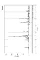
ビッカース硬度測定済の酸化物焼結体板をX線回折測定用に切り出し、X線回折測定装置(XRD)を用い、以下の条件により結晶構造を調べた。その結果、実施例1に係る酸化物焼結体においては、In2O3(ZnO)m(式中、m=2~7の整数)で表される六方晶層状化合物及び、Zn2-xSn1-yInx+yO4[0≦x<2,0≦y<1]で表されるスピネル化合物が存在することを確認した。図6に、実施例1に係る酸化物焼結体のXRDチャートを示す。
・装置:(株)リガク製Smartlab
・X線:Cu-Kα線(波長1.5418×10⁻¹⁰m)
・平行ビーム、2θ-θ反射法、連続スキャン(2.0°/分)
・サンプリング間隔:0.02°
・発散スリット(Divergence Slit、DS):1.0mm
・散乱スリット(Scattering Slit、SS):1.0mm
・受光スリット(Receiving Slit、RS):1.0mm
同様に酸化物焼結体板の余りを用い、誘導結合プラズマ発光分光分析装置(ICP-AES、株式会社島津製作所製)で酸化物焼結体の原子比を分析した。結果は次のとおりである。
Zn/(In+Sn+Zn)=0.60
Sn/(Sn+Zn)=0.20
In/(In+Sn+Zn)=0.25
実施例2~5に係る酸化物焼結体は、実施例1における焼結温度を表1に記載の焼結温度にそれぞれ変更したこと以外、実施例1と同様にして製造した。
比較例1~2に係る酸化物焼結体は、実施例1における焼結温度を表1に記載の焼結温度にそれぞれ変更したこと以外、実施例1と同様にして製造した。
比較例2に係る酸化物焼結体は、研削加工後、光学顕微鏡で観察したところ、マイクロクラックが確認された。
比較例3~4に係る酸化物焼結体は、実施例1における原料の造粒を実施せずに、金型により成形したこと、並びに焼結温度を表1に記載の焼結温度にそれぞれ変更したこと以外、実施例1と同様にして製造した。
比較例5~6に係る酸化物焼結体は、実施例1における焼結温度を表1に記載の焼結温度にそれぞれ変更したこと以外、実施例1と同様にして製造した。
次に、実施例1~5並びに比較例1~6に係る酸化物焼結体板2枚を用いて、バッキングプレートにボンディングすることで、G1サイズ:142mm×610mm(2分割)×5mmtのスパッタリングターゲットを製造した。
作製したスパッタリングターゲットを用いて、G1スパッタ装置にて、雰囲気ガスが100%Arであり、スパッタ電力が1kWである条件で1時間プレスパッタを行った。ここで、G1スパッタ装置とは、基板サイズが300mm×400mm程度の第1世代の量産用スパッタ装置のことを指す。プレスパッタの後、表2に示す成膜条件でパワーを変えて2時間連続放電を実施し、放電終了後にチャンバー開放し、クラックの有無を目視確認し、パワーを上げ、再度放電テストを繰り返すことで、クラック耐性を評価した。
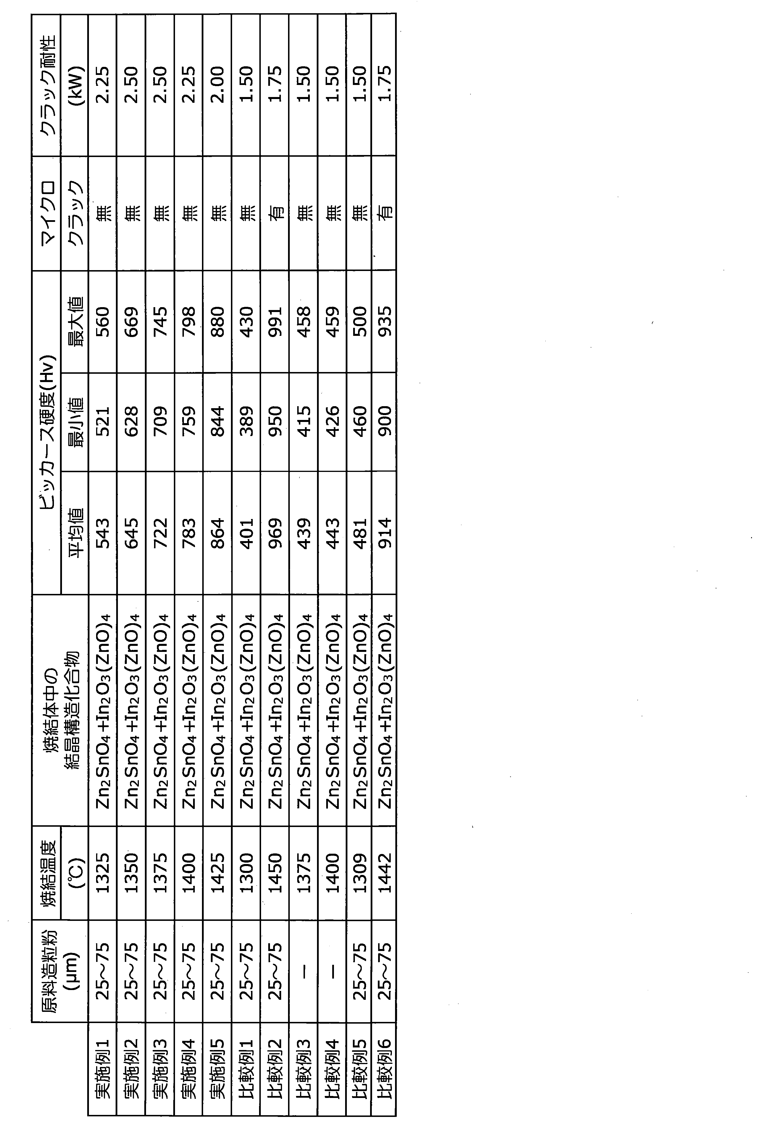
クラック耐性は、スパッタリングターゲットに割れが生じない最大限度のスパッタ電力である。クラック耐性は、1.80kW以上の場合を合格とした。各スパッタリングターゲットのクラック耐性の評価結果を表1に示す。

比較例1、3及び4に係る酸化物焼結体を用いたスパッタリングターゲットは、研削研磨の際のマイクロクラックは発生しなかったが、スパッタリング時のクラック耐性が実施例1~5よりも劣ることが分かった。比較例1、3及び4に係る酸化物焼結体の表面のビッカース硬度が低いことに起因していると考えられる。
比較例5に係る酸化物焼結体を用いたスパッタリングターゲットは、研削研磨の際のマイクロクラックは発生しなかったが、スパッタリング時のクラック耐性が実施例1~5よりも劣ることが分かった。比較例5に係る酸化物焼結体の表面のビッカース硬度が低いことに起因していると考えられる。
比較例6に係る酸化物焼結体については、研削加工後の酸化物焼結体を光学顕微鏡で観察したところ、マイクロクラックが確認された。
Claims (8)
- 酸化物焼結体であって、
前記酸化物焼結体の表面のビッカース硬度の平均値が、500Hvを超え、900Hv未満である、
酸化物焼結体。 - 請求項1に記載の酸化物焼結体を含む、スパッタリングターゲット。
- 前記酸化物焼結体は、インジウム元素、スズ元素及び亜鉛元素を含む、
請求項2に記載のスパッタリングターゲット。 - 前記酸化物焼結体は、さらに、X元素を含み、
X元素は、ゲルマニウム元素、シリコン元素、イットリウム元素、ジルコニウム元素、アルミニウム元素、マグネシウム元素、イッテルビウム元素及びガリウム元素からなる群から選択される少なくとも1種以上の元素である、
請求項3に記載のスパッタリングターゲット。 - 前記酸化物焼結体は、下記式(1)、(2)及び(3)で表される原子組成比の範囲を満たす、
請求項3または請求項4に記載のスパッタリングターゲット。
0.40≦Zn/(In+Sn+Zn)≦0.80 ・・・(1)
0.15≦Sn/(Sn+Zn)≦0.40 ・・・(2)
0.10≦In/(In+Sn+Zn)≦0.35 ・・・(3) - 前記酸化物焼結体は、In2O3(ZnO)m[m=2~7]で表わされる六方晶層状化合物及びZn2-xSn1-yInx+yO4[0≦x<2,0≦y<1]で表されるスピネル構造化合物を含む、
請求項2から請求項5のいずれか一項に記載のスパッタリングターゲット。 - 請求項2から請求項6のいずれか一項に記載のスパッタリングターゲットを製造するためのスパッタリングターゲットの製造方法であって、
前記酸化物焼結体の原料を造粒して、粒径が、25μm以上、150μm以下である原料造粒粉を得る工程と、
前記原料造粒粉を金型内に充填し、前記金型内に充填された前記原料造粒粉を成形して成形体を得る工程と、
前記成形体を、1310℃以上、1440℃以下で焼結する工程と、を含む、
スパッタリングターゲットの製造方法。 - 請求項7に記載のスパッタリングターゲットの製造方法において、
前記原料造粒粉の粒径が、25μm以上、75μm以下である、
スパッタリングターゲットの製造方法。
Priority Applications (3)
| Application Number | Priority Date | Filing Date | Title |
|---|---|---|---|
| CN202080013869.3A CN113423860A (zh) | 2019-02-18 | 2020-02-13 | 氧化物烧结体、溅射靶及溅射靶的制造方法 |
| KR1020217023912A KR102886122B1 (ko) | 2019-02-18 | 2020-02-13 | 산화물 소결체, 스퍼터링 타깃 및 스퍼터링 타깃의 제조 방법 |
| JP2021501924A JP7359836B2 (ja) | 2019-02-18 | 2020-02-13 | 酸化物焼結体、スパッタリングターゲット及びスパッタリングターゲットの製造方法 |
Applications Claiming Priority (2)
| Application Number | Priority Date | Filing Date | Title |
|---|---|---|---|
| JP2019-026785 | 2019-02-18 | ||
| JP2019026785 | 2019-02-18 |
Publications (1)
| Publication Number | Publication Date |
|---|---|
| WO2020170949A1 true WO2020170949A1 (ja) | 2020-08-27 |
Family
ID=72143793
Family Applications (1)
| Application Number | Title | Priority Date | Filing Date |
|---|---|---|---|
| PCT/JP2020/005666 Ceased WO2020170949A1 (ja) | 2019-02-18 | 2020-02-13 | 酸化物焼結体、スパッタリングターゲット及びスパッタリングターゲットの製造方法 |
Country Status (5)
| Country | Link |
|---|---|
| JP (1) | JP7359836B2 (ja) |
| KR (1) | KR102886122B1 (ja) |
| CN (1) | CN113423860A (ja) |
| TW (1) | TWI842834B (ja) |
| WO (1) | WO2020170949A1 (ja) |
Cited By (2)
| Publication number | Priority date | Publication date | Assignee | Title |
|---|---|---|---|---|
| CN116253556A (zh) * | 2023-02-07 | 2023-06-13 | 郑州大学 | 氧化铟锡锌靶材及其制备方法 |
| CN118530006A (zh) * | 2023-02-22 | 2024-08-23 | 超威电源集团有限公司 | 薄膜镁电池钴酸铝镁正极靶材、制备方法及薄膜镁电池 |
Families Citing this family (2)
| Publication number | Priority date | Publication date | Assignee | Title |
|---|---|---|---|---|
| TWI832292B (zh) * | 2022-06-17 | 2024-02-11 | 南臺學校財團法人南臺科技大學 | 簇式多孔隙金屬氧化物的製造方法 |
| KR102869632B1 (ko) * | 2024-12-02 | 2025-10-14 | 주식회사 에이치앤이루자 | 소결체, 스퍼터링 타겟, 산화물 박막, 박막 트랜지스터 및 소결체의 제조방법 |
Citations (4)
| Publication number | Priority date | Publication date | Assignee | Title |
|---|---|---|---|---|
| WO2007026783A1 (ja) * | 2005-09-01 | 2007-03-08 | Idemitsu Kosan Co., Ltd. | スパッタリングターゲット、透明導電膜及び透明電極 |
| WO2007034749A1 (ja) * | 2005-09-22 | 2007-03-29 | Idemitsu Kosan Co., Ltd. | 酸化物材料、及びスパッタリングターゲット |
| WO2007058318A1 (ja) * | 2005-11-21 | 2007-05-24 | Idemitsu Kosan Co., Ltd. | 焼成体及びその製造方法 |
| WO2017122618A1 (ja) * | 2016-01-15 | 2017-07-20 | 住友化学株式会社 | 非晶質複合金属酸化物の製造方法 |
Family Cites Families (9)
| Publication number | Priority date | Publication date | Assignee | Title |
|---|---|---|---|---|
| US8623511B2 (en) * | 2008-06-06 | 2014-01-07 | Idemitsu Kosan Co., Ltd. | Sputtering target for oxide thin film and process for producing the sputtering target |
| JP4843083B2 (ja) * | 2009-11-19 | 2011-12-21 | 出光興産株式会社 | In−Ga−Zn系酸化物スパッタリングターゲット |
| JP2012180247A (ja) | 2011-03-02 | 2012-09-20 | Kobelco Kaken:Kk | 酸化物焼結体およびスパッタリングターゲット |
| WO2012153507A1 (ja) * | 2011-05-10 | 2012-11-15 | 出光興産株式会社 | In2O3-SnO2-ZnO系スパッタリングターゲット |
| JP6082735B2 (ja) * | 2012-05-31 | 2017-02-15 | 出光興産株式会社 | スパッタリングターゲット |
| JPWO2016017605A1 (ja) * | 2014-07-31 | 2017-05-25 | 住友化学株式会社 | 酸化物焼結体 |
| JP6041219B2 (ja) * | 2014-08-27 | 2016-12-07 | 日立金属株式会社 | スパッタリングターゲット |
| JP2017154910A (ja) * | 2016-02-29 | 2017-09-07 | 住友金属鉱山株式会社 | 酸化物焼結体及びスパッタリング用ターゲット |
| TWI720188B (zh) * | 2016-04-26 | 2021-03-01 | 日商出光興產股份有限公司 | 氧化物燒結體、濺鍍靶及氧化物半導體膜 |
-
2020
- 2020-02-13 KR KR1020217023912A patent/KR102886122B1/ko active Active
- 2020-02-13 WO PCT/JP2020/005666 patent/WO2020170949A1/ja not_active Ceased
- 2020-02-13 CN CN202080013869.3A patent/CN113423860A/zh active Pending
- 2020-02-13 JP JP2021501924A patent/JP7359836B2/ja active Active
- 2020-02-18 TW TW109105207A patent/TWI842834B/zh active
Patent Citations (4)
| Publication number | Priority date | Publication date | Assignee | Title |
|---|---|---|---|---|
| WO2007026783A1 (ja) * | 2005-09-01 | 2007-03-08 | Idemitsu Kosan Co., Ltd. | スパッタリングターゲット、透明導電膜及び透明電極 |
| WO2007034749A1 (ja) * | 2005-09-22 | 2007-03-29 | Idemitsu Kosan Co., Ltd. | 酸化物材料、及びスパッタリングターゲット |
| WO2007058318A1 (ja) * | 2005-11-21 | 2007-05-24 | Idemitsu Kosan Co., Ltd. | 焼成体及びその製造方法 |
| WO2017122618A1 (ja) * | 2016-01-15 | 2017-07-20 | 住友化学株式会社 | 非晶質複合金属酸化物の製造方法 |
Cited By (2)
| Publication number | Priority date | Publication date | Assignee | Title |
|---|---|---|---|---|
| CN116253556A (zh) * | 2023-02-07 | 2023-06-13 | 郑州大学 | 氧化铟锡锌靶材及其制备方法 |
| CN118530006A (zh) * | 2023-02-22 | 2024-08-23 | 超威电源集团有限公司 | 薄膜镁电池钴酸铝镁正极靶材、制备方法及薄膜镁电池 |
Also Published As
| Publication number | Publication date |
|---|---|
| KR20210129040A (ko) | 2021-10-27 |
| TWI842834B (zh) | 2024-05-21 |
| JPWO2020170949A1 (ja) | 2021-12-23 |
| TW202041483A (zh) | 2020-11-16 |
| CN113423860A (zh) | 2021-09-21 |
| JP7359836B2 (ja) | 2023-10-11 |
| KR102886122B1 (ko) | 2025-11-13 |
Similar Documents
| Publication | Publication Date | Title |
|---|---|---|
| JP7359836B2 (ja) | 酸化物焼結体、スパッタリングターゲット及びスパッタリングターゲットの製造方法 | |
| JP6307344B2 (ja) | 酸化物焼結体及びスパッタリングターゲット | |
| JP4891381B2 (ja) | In−Ga−Zn系焼結体、及びスパッタリングターゲット | |
| JP2011106002A (ja) | In−Ga−Zn系酸化物スパッタリングターゲット | |
| JP6166207B2 (ja) | 酸化物焼結体及びスパッタリングターゲット | |
| JP6231924B2 (ja) | 酸化物焼結体及びスパッタリングターゲット | |
| JP7456992B2 (ja) | 酸化物焼結体、スパッタリングターゲット及びスパッタリングターゲットの製造方法 | |
| JP2011195924A (ja) | In−Ga−Zn系複合酸化物焼結体およびその製造方法 | |
| TWI774687B (zh) | 氧化物燒結體及其製造方法、濺鍍靶、以及半導體裝置之製造方法 | |
| JP6158129B2 (ja) | 酸化物焼結体及びスパッタリングターゲット | |
| JP6781931B2 (ja) | スパッタリングターゲット材 | |
| JP2015214437A (ja) | 酸化物焼結体及びスパッタリングターゲット | |
| JP2011195409A (ja) | In−Ga−Zn系複合酸化物焼結体およびその製造方法 | |
| JP6774624B2 (ja) | 酸化物ターゲット材 | |
| US12173398B2 (en) | Cr—Si sintered body, sputtering target, and method for producing thin film | |
| JP5526905B2 (ja) | 導電性酸化物焼結体の製造方法 | |
| JP6788151B1 (ja) | 焼結体 | |
| TW201336803A (zh) | 氧化物燒結體及濺鍍靶,以及其製造方法 | |
| WO2025220265A1 (ja) | 焼結体及びスパッタリングターゲット並びに焼結体の製造方法 | |
| WO2025182965A1 (ja) | 焼結体及びスパッタリングターゲット並びに焼結体の製造方法 | |
| JP2012056842A (ja) | In−Ga−Zn系酸化物、酸化物焼結体、及びスパッタリングターゲット |
Legal Events
| Date | Code | Title | Description |
|---|---|---|---|
| 121 | Ep: the epo has been informed by wipo that ep was designated in this application |
Ref document number: 20758806 Country of ref document: EP Kind code of ref document: A1 |
|
| ENP | Entry into the national phase |
Ref document number: 2021501924 Country of ref document: JP Kind code of ref document: A Ref document number: 20217023912 Country of ref document: KR Kind code of ref document: A |
|
| NENP | Non-entry into the national phase |
Ref country code: DE |
|
| 122 | Ep: pct application non-entry in european phase |
Ref document number: 20758806 Country of ref document: EP Kind code of ref document: A1 |