WO2020149401A1 - 金属材および接続端子 - Google Patents
金属材および接続端子 Download PDFInfo
- Publication number
- WO2020149401A1 WO2020149401A1 PCT/JP2020/001479 JP2020001479W WO2020149401A1 WO 2020149401 A1 WO2020149401 A1 WO 2020149401A1 JP 2020001479 W JP2020001479 W JP 2020001479W WO 2020149401 A1 WO2020149401 A1 WO 2020149401A1
- Authority
- WO
- WIPO (PCT)
- Prior art keywords
- surface layer
- layer
- metal material
- metal
- concentration
- Prior art date
- Legal status (The legal status is an assumption and is not a legal conclusion. Google has not performed a legal analysis and makes no representation as to the accuracy of the status listed.)
- Ceased
Links
Images



Classifications
-
- C—CHEMISTRY; METALLURGY
- C23—COATING METALLIC MATERIAL; COATING MATERIAL WITH METALLIC MATERIAL; CHEMICAL SURFACE TREATMENT; DIFFUSION TREATMENT OF METALLIC MATERIAL; COATING BY VACUUM EVAPORATION, BY SPUTTERING, BY ION IMPLANTATION OR BY CHEMICAL VAPOUR DEPOSITION, IN GENERAL; INHIBITING CORROSION OF METALLIC MATERIAL OR INCRUSTATION IN GENERAL
- C23C—COATING METALLIC MATERIAL; COATING MATERIAL WITH METALLIC MATERIAL; SURFACE TREATMENT OF METALLIC MATERIAL BY DIFFUSION INTO THE SURFACE, BY CHEMICAL CONVERSION OR SUBSTITUTION; COATING BY VACUUM EVAPORATION, BY SPUTTERING, BY ION IMPLANTATION OR BY CHEMICAL VAPOUR DEPOSITION, IN GENERAL
- C23C28/00—Coating for obtaining at least two superposed coatings either by methods not provided for in a single one of groups C23C2/00 - C23C26/00 or by combinations of methods provided for in subclasses C23C and C25C or C25D
- C23C28/02—Coating for obtaining at least two superposed coatings either by methods not provided for in a single one of groups C23C2/00 - C23C26/00 or by combinations of methods provided for in subclasses C23C and C25C or C25D only coatings only including layers of metallic material
-
- H—ELECTRICITY
- H01—ELECTRIC ELEMENTS
- H01R—ELECTRICALLY-CONDUCTIVE CONNECTIONS; STRUCTURAL ASSOCIATIONS OF A PLURALITY OF MUTUALLY-INSULATED ELECTRICAL CONNECTING ELEMENTS; COUPLING DEVICES; CURRENT COLLECTORS
- H01R13/00—Details of coupling devices of the kinds covered by groups H01R12/70 or H01R24/00 - H01R33/00
- H01R13/02—Contact members
- H01R13/03—Contact members characterised by the material, e.g. plating, or coating materials
-
- B—PERFORMING OPERATIONS; TRANSPORTING
- B32—LAYERED PRODUCTS
- B32B—LAYERED PRODUCTS, i.e. PRODUCTS BUILT-UP OF STRATA OF FLAT OR NON-FLAT, e.g. CELLULAR OR HONEYCOMB, FORM
- B32B15/00—Layered products comprising a layer of metal
- B32B15/01—Layered products comprising a layer of metal all layers being exclusively metallic
-
- B—PERFORMING OPERATIONS; TRANSPORTING
- B32—LAYERED PRODUCTS
- B32B—LAYERED PRODUCTS, i.e. PRODUCTS BUILT-UP OF STRATA OF FLAT OR NON-FLAT, e.g. CELLULAR OR HONEYCOMB, FORM
- B32B15/00—Layered products comprising a layer of metal
- B32B15/01—Layered products comprising a layer of metal all layers being exclusively metallic
- B32B15/018—Layered products comprising a layer of metal all layers being exclusively metallic one layer being formed of a noble metal or a noble metal alloy
-
- C—CHEMISTRY; METALLURGY
- C23—COATING METALLIC MATERIAL; COATING MATERIAL WITH METALLIC MATERIAL; CHEMICAL SURFACE TREATMENT; DIFFUSION TREATMENT OF METALLIC MATERIAL; COATING BY VACUUM EVAPORATION, BY SPUTTERING, BY ION IMPLANTATION OR BY CHEMICAL VAPOUR DEPOSITION, IN GENERAL; INHIBITING CORROSION OF METALLIC MATERIAL OR INCRUSTATION IN GENERAL
- C23C—COATING METALLIC MATERIAL; COATING MATERIAL WITH METALLIC MATERIAL; SURFACE TREATMENT OF METALLIC MATERIAL BY DIFFUSION INTO THE SURFACE, BY CHEMICAL CONVERSION OR SUBSTITUTION; COATING BY VACUUM EVAPORATION, BY SPUTTERING, BY ION IMPLANTATION OR BY CHEMICAL VAPOUR DEPOSITION, IN GENERAL
- C23C18/00—Chemical coating by decomposition of either liquid compounds or solutions of the coating forming compounds, without leaving reaction products of surface material in the coating; Contact plating
- C23C18/16—Chemical coating by decomposition of either liquid compounds or solutions of the coating forming compounds, without leaving reaction products of surface material in the coating; Contact plating by reduction or substitution, e.g. electroless plating
- C23C18/1601—Process or apparatus
- C23C18/1633—Process of electroless plating
- C23C18/1646—Characteristics of the product obtained
- C23C18/165—Multilayered product
- C23C18/1651—Two or more layers only obtained by electroless plating
-
- C—CHEMISTRY; METALLURGY
- C23—COATING METALLIC MATERIAL; COATING MATERIAL WITH METALLIC MATERIAL; CHEMICAL SURFACE TREATMENT; DIFFUSION TREATMENT OF METALLIC MATERIAL; COATING BY VACUUM EVAPORATION, BY SPUTTERING, BY ION IMPLANTATION OR BY CHEMICAL VAPOUR DEPOSITION, IN GENERAL; INHIBITING CORROSION OF METALLIC MATERIAL OR INCRUSTATION IN GENERAL
- C23C—COATING METALLIC MATERIAL; COATING MATERIAL WITH METALLIC MATERIAL; SURFACE TREATMENT OF METALLIC MATERIAL BY DIFFUSION INTO THE SURFACE, BY CHEMICAL CONVERSION OR SUBSTITUTION; COATING BY VACUUM EVAPORATION, BY SPUTTERING, BY ION IMPLANTATION OR BY CHEMICAL VAPOUR DEPOSITION, IN GENERAL
- C23C28/00—Coating for obtaining at least two superposed coatings either by methods not provided for in a single one of groups C23C2/00 - C23C26/00 or by combinations of methods provided for in subclasses C23C and C25C or C25D
- C23C28/02—Coating for obtaining at least two superposed coatings either by methods not provided for in a single one of groups C23C2/00 - C23C26/00 or by combinations of methods provided for in subclasses C23C and C25C or C25D only coatings only including layers of metallic material
- C23C28/021—Coating for obtaining at least two superposed coatings either by methods not provided for in a single one of groups C23C2/00 - C23C26/00 or by combinations of methods provided for in subclasses C23C and C25C or C25D only coatings only including layers of metallic material including at least one metal alloy layer
-
- C—CHEMISTRY; METALLURGY
- C23—COATING METALLIC MATERIAL; COATING MATERIAL WITH METALLIC MATERIAL; CHEMICAL SURFACE TREATMENT; DIFFUSION TREATMENT OF METALLIC MATERIAL; COATING BY VACUUM EVAPORATION, BY SPUTTERING, BY ION IMPLANTATION OR BY CHEMICAL VAPOUR DEPOSITION, IN GENERAL; INHIBITING CORROSION OF METALLIC MATERIAL OR INCRUSTATION IN GENERAL
- C23C—COATING METALLIC MATERIAL; COATING MATERIAL WITH METALLIC MATERIAL; SURFACE TREATMENT OF METALLIC MATERIAL BY DIFFUSION INTO THE SURFACE, BY CHEMICAL CONVERSION OR SUBSTITUTION; COATING BY VACUUM EVAPORATION, BY SPUTTERING, BY ION IMPLANTATION OR BY CHEMICAL VAPOUR DEPOSITION, IN GENERAL
- C23C28/00—Coating for obtaining at least two superposed coatings either by methods not provided for in a single one of groups C23C2/00 - C23C26/00 or by combinations of methods provided for in subclasses C23C and C25C or C25D
- C23C28/02—Coating for obtaining at least two superposed coatings either by methods not provided for in a single one of groups C23C2/00 - C23C26/00 or by combinations of methods provided for in subclasses C23C and C25C or C25D only coatings only including layers of metallic material
- C23C28/023—Coating for obtaining at least two superposed coatings either by methods not provided for in a single one of groups C23C2/00 - C23C26/00 or by combinations of methods provided for in subclasses C23C and C25C or C25D only coatings only including layers of metallic material only coatings of metal elements only
-
- C—CHEMISTRY; METALLURGY
- C23—COATING METALLIC MATERIAL; COATING MATERIAL WITH METALLIC MATERIAL; CHEMICAL SURFACE TREATMENT; DIFFUSION TREATMENT OF METALLIC MATERIAL; COATING BY VACUUM EVAPORATION, BY SPUTTERING, BY ION IMPLANTATION OR BY CHEMICAL VAPOUR DEPOSITION, IN GENERAL; INHIBITING CORROSION OF METALLIC MATERIAL OR INCRUSTATION IN GENERAL
- C23C—COATING METALLIC MATERIAL; COATING MATERIAL WITH METALLIC MATERIAL; SURFACE TREATMENT OF METALLIC MATERIAL BY DIFFUSION INTO THE SURFACE, BY CHEMICAL CONVERSION OR SUBSTITUTION; COATING BY VACUUM EVAPORATION, BY SPUTTERING, BY ION IMPLANTATION OR BY CHEMICAL VAPOUR DEPOSITION, IN GENERAL
- C23C28/00—Coating for obtaining at least two superposed coatings either by methods not provided for in a single one of groups C23C2/00 - C23C26/00 or by combinations of methods provided for in subclasses C23C and C25C or C25D
- C23C28/30—Coatings combining at least one metallic layer and at least one inorganic non-metallic layer
- C23C28/32—Coatings combining at least one metallic layer and at least one inorganic non-metallic layer including at least one pure metallic layer
- C23C28/321—Coatings combining at least one metallic layer and at least one inorganic non-metallic layer including at least one pure metallic layer with at least one metal alloy layer
-
- C—CHEMISTRY; METALLURGY
- C23—COATING METALLIC MATERIAL; COATING MATERIAL WITH METALLIC MATERIAL; CHEMICAL SURFACE TREATMENT; DIFFUSION TREATMENT OF METALLIC MATERIAL; COATING BY VACUUM EVAPORATION, BY SPUTTERING, BY ION IMPLANTATION OR BY CHEMICAL VAPOUR DEPOSITION, IN GENERAL; INHIBITING CORROSION OF METALLIC MATERIAL OR INCRUSTATION IN GENERAL
- C23C—COATING METALLIC MATERIAL; COATING MATERIAL WITH METALLIC MATERIAL; SURFACE TREATMENT OF METALLIC MATERIAL BY DIFFUSION INTO THE SURFACE, BY CHEMICAL CONVERSION OR SUBSTITUTION; COATING BY VACUUM EVAPORATION, BY SPUTTERING, BY ION IMPLANTATION OR BY CHEMICAL VAPOUR DEPOSITION, IN GENERAL
- C23C28/00—Coating for obtaining at least two superposed coatings either by methods not provided for in a single one of groups C23C2/00 - C23C26/00 or by combinations of methods provided for in subclasses C23C and C25C or C25D
- C23C28/30—Coatings combining at least one metallic layer and at least one inorganic non-metallic layer
- C23C28/32—Coatings combining at least one metallic layer and at least one inorganic non-metallic layer including at least one pure metallic layer
- C23C28/322—Coatings combining at least one metallic layer and at least one inorganic non-metallic layer including at least one pure metallic layer only coatings of metal elements only
-
- C—CHEMISTRY; METALLURGY
- C23—COATING METALLIC MATERIAL; COATING MATERIAL WITH METALLIC MATERIAL; CHEMICAL SURFACE TREATMENT; DIFFUSION TREATMENT OF METALLIC MATERIAL; COATING BY VACUUM EVAPORATION, BY SPUTTERING, BY ION IMPLANTATION OR BY CHEMICAL VAPOUR DEPOSITION, IN GENERAL; INHIBITING CORROSION OF METALLIC MATERIAL OR INCRUSTATION IN GENERAL
- C23C—COATING METALLIC MATERIAL; COATING MATERIAL WITH METALLIC MATERIAL; SURFACE TREATMENT OF METALLIC MATERIAL BY DIFFUSION INTO THE SURFACE, BY CHEMICAL CONVERSION OR SUBSTITUTION; COATING BY VACUUM EVAPORATION, BY SPUTTERING, BY ION IMPLANTATION OR BY CHEMICAL VAPOUR DEPOSITION, IN GENERAL
- C23C28/00—Coating for obtaining at least two superposed coatings either by methods not provided for in a single one of groups C23C2/00 - C23C26/00 or by combinations of methods provided for in subclasses C23C and C25C or C25D
- C23C28/30—Coatings combining at least one metallic layer and at least one inorganic non-metallic layer
- C23C28/34—Coatings combining at least one metallic layer and at least one inorganic non-metallic layer including at least one inorganic non-metallic material layer, e.g. metal carbide, nitride, boride, silicide layer and their mixtures, enamels, phosphates and sulphates
- C23C28/345—Coatings combining at least one metallic layer and at least one inorganic non-metallic layer including at least one inorganic non-metallic material layer, e.g. metal carbide, nitride, boride, silicide layer and their mixtures, enamels, phosphates and sulphates with at least one oxide layer
-
- C—CHEMISTRY; METALLURGY
- C23—COATING METALLIC MATERIAL; COATING MATERIAL WITH METALLIC MATERIAL; CHEMICAL SURFACE TREATMENT; DIFFUSION TREATMENT OF METALLIC MATERIAL; COATING BY VACUUM EVAPORATION, BY SPUTTERING, BY ION IMPLANTATION OR BY CHEMICAL VAPOUR DEPOSITION, IN GENERAL; INHIBITING CORROSION OF METALLIC MATERIAL OR INCRUSTATION IN GENERAL
- C23C—COATING METALLIC MATERIAL; COATING MATERIAL WITH METALLIC MATERIAL; SURFACE TREATMENT OF METALLIC MATERIAL BY DIFFUSION INTO THE SURFACE, BY CHEMICAL CONVERSION OR SUBSTITUTION; COATING BY VACUUM EVAPORATION, BY SPUTTERING, BY ION IMPLANTATION OR BY CHEMICAL VAPOUR DEPOSITION, IN GENERAL
- C23C30/00—Coating with metallic material characterised only by the composition of the metallic material, i.e. not characterised by the coating process
-
- H—ELECTRICITY
- H01—ELECTRIC ELEMENTS
- H01R—ELECTRICALLY-CONDUCTIVE CONNECTIONS; STRUCTURAL ASSOCIATIONS OF A PLURALITY OF MUTUALLY-INSULATED ELECTRICAL CONNECTING ELEMENTS; COUPLING DEVICES; CURRENT COLLECTORS
- H01R13/00—Details of coupling devices of the kinds covered by groups H01R12/70 or H01R24/00 - H01R33/00
- H01R13/02—Contact members
- H01R13/10—Sockets for co-operation with pins or blades
- H01R13/11—Resilient sockets
- H01R13/111—Resilient sockets co-operating with pins having a circular transverse section
Definitions
- the present disclosure relates to metal materials and connection terminals.
- Au layer may be provided on the surface of an electrical connection member such as a connection terminal.
- Gold (Au) has high electrical conductivity and high melting point, and is also resistant to oxidation. Therefore, when a high temperature environment is assumed, the electrical connecting member having the Au layer on its surface can be preferably used. For example, in an automobile, if a connection terminal having an Au layer on its surface is used as a connection terminal used in a high temperature environment such as around an engine, the surface of the Au layer maintains a low contact resistance even at high temperatures. In addition, stable electrical connection characteristics can be obtained.
- Au is a relatively soft metal, and when it is provided on the surface of an electrical connection member such as a connection terminal, lack of hardness tends to be a problem such as an increase in friction coefficient during sliding. Therefore, hard gold having a hardness higher than that of pure Au may be used.
- a plating solution to which an additive element such as Co is added is used. By containing a small amount of Co in the Au layer formed by plating, the hardness of the Au layer is increased.
- the Au is a metal which is not easily oxidized, it is easy to keep the surface of the surface of the electrical connection member such as the connection terminal with a low contact resistance by providing the Au layer on the surface.
- additional elements such as Co contained in the hard gold diffuse to the surface, May undergo oxidation. Then, the contact resistance of the surface may increase due to the contribution of the oxide of the additional element.
- metals such as Ni that are more easily oxidized than Au are often present below the Au layer as a base material or an intermediate layer. Even when these metals diffuse to the surface of the Au layer during heating and undergo oxidation, the contact resistance of the surface may increase due to the contribution of the oxides of these metals.
- the metal material of the present disclosure has a base material and a surface layer formed on the base material, and the surface layer contains Au and In, and at least In is present on the outermost surface. ..
- connection terminal of the present disclosure is made of the metal material as described above, and the surface layer is formed on the surface of the base material at least at a contact portion that makes electrical contact with the counterpart conductive member.
- the metal material and the connection terminal of the present disclosure have a surface layer containing Au, and can maintain a low contact resistance state even when heated.
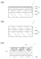
- FIG. 1A to 1C are cross-sectional views schematically showing a laminated structure of a metal material according to an embodiment of the present disclosure.
- FIG. 1A shows the configuration of the entire cross section in the case where the surface layer has a multi-layer structure and
- FIG. 1B shows the example when the surface layer has a single-layer structure.
- FIG. 1C is an enlarged view showing an example of the state of the surface layer having a single layer structure.
- FIG. 2 is a cross-sectional view illustrating the outline of the connection terminal according to the embodiment of the present disclosure.
- 3A to 3C are diagrams showing element concentration distributions of each sample after heating, which are obtained by depth analysis Auger electron spectroscopy. 3A shows the sample A1, FIG. 3B shows the sample A2, and FIG. 3C shows the sample B1.
- FIG. 4 is a diagram showing a result of X-ray diffraction for the sample A1.
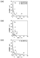
- 5A to 5C are diagrams showing the contact resistance of each sample in the initial state and the state after heating.
- 5A shows sample A1
- FIG. 5B shows sample A2
- FIG. 5C shows sample B1.
- the metal material of the present disclosure has a base material and a surface layer formed on the base material, and the surface layer contains Au and In, and at least In is present on the outermost surface. ..
- the metal material according to the present disclosure contains In in addition to Au in the surface layer.
- In it is possible to suppress the diffusion of the metal (other metal) other than Au and In existing in or under the surface layer to the outermost surface when the temperature of the metal material becomes high. You can As a result, an increase in contact resistance due to the oxidation of another metal on the outermost surface is less likely to occur, and the low contact resistance obtained by Au's high electrical conductivity and oxidation resistance can be maintained before and after heating. it can. Even if In is oxidized on the outermost surface, the oxide film is easily destroyed by application of a load or the like, and thus it is difficult to contribute to increase in contact resistance.
- At least one of the surface layer and the base material contains an easily oxidizable metal other than In that is more susceptible to oxidation than Au, and when the metal material is heated at 170° C.
- the increase in the concentration of the easily oxidizable metal is preferably below the detection limit by Auger electron spectroscopy. In this case, it means that due to the effect of containing In in the surface layer, diffusion of the oxidizable metal to the outermost surface can be sufficiently suppressed when the metal material is heated. Therefore, the increase in contact resistance due to the oxidation of the oxidizable metal on the outermost surface can be effectively suppressed.
- At least a part of In in the surface layer preferably constitutes an Au—In alloy.
- the surface layer containing In in addition to Au can be stably formed and easily maintained.
- the Au—In alloy has an effect of suppressing diffusion of other metal existing in the layer of the surface layer or under the surface layer to the outermost surface due to the contribution of In.
- the oxide film formed on the surface has a property of being easily broken. Therefore, the Au—In alloy exhibits an excellent effect in suppressing an increase in contact resistance during heating in the surface layer.
- the Au—In alloy is preferably a solid solution in which In is solid-dissolved in Au. Then, since In has a characteristic of being easily solid-dissolved in Au, a surface layer containing In in addition to Au can be stably formed, and environmental stability becomes high.
- both Au and In should be present on the outermost surface. Then, both the high electrical conductivity and the hard-to-oxidize property of Au and the effect of suppressing the diffusion of other metals by In are effectively utilized on the outermost surface to form a surface layer having a low contact resistance before and after heating. You can
- the surface layer may include an Au portion containing Au as a main component and a high-concentration In portion containing a higher concentration of In than the Au portion. Then, the high-concentration In portion having a high In concentration is formed, so that the high-concentration In portion can effectively achieve the diffusion suppression of the other metal.
- the high concentration In portion is preferably formed on the surface of the Au portion and exposed on the outermost surface. Then, since the high-concentration In portion constitutes the outermost surface of the surface layer, it is possible to effectively suppress an increase in contact resistance due to the diffusion and oxidation of other metal on the outermost surface during heating. it can.
- the entire surface layer may have a single-layer structure configured as a single layer containing an Au—In alloy.
- the inclusion of In can suppress the diffusion and oxidation of other metal to the outermost surface due to heating.
- the surface layer having a single-layer structure is composed of a homogeneous Au—In alloy as a whole, there are two types of phases, an Au portion having a relatively high Au concentration and a high concentration In portion having a relatively high In concentration. May have.
- the Au layer and the In layer are laminated in this order to form the surface layer, if the In content relative to Au is increased, a single layer structure is likely to be formed.
- In is preferably distributed in the surface layer at a depth of at least 0.01 ⁇ m from the outermost surface. Further, in the surface layer, In may be distributed in a region from the outermost surface to a depth of at least 0.05 ⁇ m. Then, due to In, it becomes easy to sufficiently suppress the diffusion of other metal and the increase in contact resistance during heating.
- the base material has an intermediate layer formed on a base material, and the intermediate layer preferably contains at least one of Ni, Cr, Mn, Fe, Co, and Cu. Then, those metals are metals that are easily oxidized, but since the surface layer contains In, it diffuses into the surface layer during heating and is oxidized, and it becomes difficult to contribute to increase the contact resistance. ..
- the above surface layer preferably contains Co. Then, the hardness of the surface layer can be increased by the effect of containing Co.
- Co is a metal that easily diffuses into the surface of the layer containing Au and is oxidized during heating to increase the contact resistance, but the inclusion of In in the surface layer suppresses the diffusion of Co and reduces the contact. A low resistance state is easily maintained.
- the content of additive elements other than Au and In in the surface layer is preferably 5% or less. Then, the characteristics imparted to the surface layer by Au and In are not easily impaired by the addition of the additional element.
- the content of In in the surface layer as a whole is preferably 10% or more in terms of atomic ratio with respect to Au. Then, the characteristics imparted to the surface layer by In, such as suppressing diffusion of other metals, are effectively exhibited.
- the content of In in the surface layer as a whole is preferably smaller than Au in terms of the number of atoms. Then, the characteristics imparted to the surface layer by Au, such as reduction of the contact resistance on the surface, are effectively exhibited.
- the thickness of the surface layer is preferably 0.1 ⁇ m or more. Then, the characteristics of the surface layer provided by Au and In can be sufficiently exhibited.
- connection terminal according to the present disclosure is made of the metal material, and the surface layer is formed on the surface of the base material at least at a contact portion that makes electrical contact with the counterpart conductive member.
- the surface layer as described above is formed at least in the contact portion, so that the contact portion can maintain low contact resistance even after being heated.
- the content (concentration) of each element is indicated by the atomic number ratio such as atomic% as a unit.
- the case where an unavoidable impurity is contained in the elemental metal is also included.
- the alloy includes both a solid solution and an intermetallic compound.
- a certain metal element as a main component means a state in which the element occupies 50 atomic% or more of all metal species.
- a metal material according to an embodiment of the present disclosure is configured by stacking metal materials.
- the metal material according to the embodiment of the present disclosure may be any metal member, but can be preferably used as a material for forming an electrical connection member such as a connection terminal.
- composition of metal material 1A and 1B show an example of a laminated structure of a metal material 1 according to an embodiment of the present disclosure.
- the metal material 1 has a base material 10 and a surface layer 11 formed on the surface of the base material 10 and exposed on the outermost surface.
- the surface layer 11 contains gold (Au) and indium (In), and may have a multi-layer structure as shown in FIG. 1A or a single-layer structure as shown in FIG. 1B.
- a thin film (not shown) such as an organic layer may be provided on the surface layer 11 exposed on the outermost surface of the metal material 1 as long as the characteristics of the surface layer 11 are not impaired.
- the base material 10 may be made of a single metal material, but preferably includes a base material 10a and an intermediate layer 10b.
- the intermediate layer 10b is formed on the surface of the base material 10a as a metal layer thinner than the base material 10a.
- the base material 10a can be made of a metal material having an arbitrary shape such as a plate shape.
- the material forming the base material 10a is not particularly limited, but when the metal material 1 forms an electric connection member such as a connection terminal, Cu is used as the material forming the base material 10a.
- Cu alloy, Al or Al alloy, Fe or Fe alloy, or the like can be preferably used. Among them, Cu or Cu alloy having excellent electric conductivity can be preferably used.
- the material forming the intermediate layer 10b include metal materials containing at least one selected from the group (A group) of Ni, Cr, Mn, Fe, Co, and Cu.
- the material forming the intermediate layer 10b may be a single metal composed of one kind selected from the group A, or an alloy containing one kind or two or more kinds of metal elements selected from the group A. ..
- the intermediate layer 10b may be composed of only one layer or may be a laminate of two or more layers. Even when the base material 10 does not have the intermediate layer 10b and is made of a single metal material, at least the surface of the single metal material contains at least one selected from the group A. It is preferably composed of
- the intermediate layer 10b contains as a main component a metal containing at least one selected from the group A, particularly a metal element selected from the group A.
- the Cu composition diffuses from the base material 10a to the surface layer 11, and further influences the composition and characteristics of the surface layer 11 such as consumption of In due to alloying with the diffused Cu. It is possible to effectively suppress the occurrence of the phenomenon even under high temperature conditions.
- the intermediate layer 10b is made of Ni or an alloy containing Ni as a main component, it is possible to effectively achieve the suppression of Cu diffusion into the surface layer 11.
- the thickness of the intermediate layer 10b is not particularly limited, it is preferably 0.1 ⁇ m or more from the viewpoint of effectively achieving diffusion suppression between the base material 10a and the surface layer 11. On the other hand, from the viewpoint of avoiding forming the excessively thick intermediate layer 10b, its thickness is preferably 3 ⁇ m or less.
- a part of the base material 10a side may form an alloy with the constituent element of the base material 10a, and a part of the surface layer 11 side forms an alloy with the constituent element of the surface layer 11. May be.
- the surface layer 11 is formed as a metal layer containing Au and In.
- the surface layer 11 may contain an element other than Au and In.
- an element having an effect of hardening Au such as Co can be exemplified.
- the content of the additive element such as Co in the surface layer 11 is preferably suppressed to 5% or less so as not to impair the characteristics imparted by Au and In as described below.
- Au and In may be contained in the surface layer 11 as long as Au and In are contained and at least In atoms are present on the outermost surface.
- Au and In may each be in the state of a simple metal or may form an alloy.
- a part that is a simple metal and a part that is an alloy may coexist.
- at least a part of In contained in the surface layer 11, and preferably most of In contained in the surface layer 11, is Au—In. It preferably comprises an alloy.
- the Au—In alloy may be a solid solution or an intermetallic compound, but it is easy to form a solid solution in which In is solid-solved in the Au lattice.
- the surface layer 11 has a multi-layer structure in which a plurality of layers (11a, 11b) having different component compositions are laminated as shown in FIG. 1A, a clear laminated structure is obtained as shown in FIG. 1B. It may have a single layer structure in which the whole is configured as a single layer. Further, when a single layer structure is adopted, even if only a single alloy phase is formed in the surface layer 11, as shown in FIG. 1C, a plurality of phases (11a, 11b) are formed in the layer. It may be in a mixed state.
- the surface layer 11 when the Au layer as a raw material layer and the In layer are laminated in this order to form the surface layer 11, if the In layer is made thin, the surface layer 11 easily has a multi-layer structure, If the In layer is relatively thick and the In content with respect to Au is high, a single layer structure can be easily obtained.
- the surface layer 11 may be made of a homogenous Au—In alloy as a whole, especially when it has a single-layer structure. However, regardless of whether it has a single-layer structure or a multi-layer structure, it is necessary to have two phases, an Au part 11a having a relatively high Au concentration and a high-concentration In part 11b having a relatively high In concentration. Is preferred.
- the layer (lower layer) on the side of the base material 10 is composed of the Au portion 11a, and the layer formed on the surface of the Au portion 11a and exposed on the outermost surface.
- the (upper layer) can be composed of the high-concentration In portion 11b.
- the surface layer 11 having the single-layer structure shown in FIG. 1B may have a structure in which the Au portion 11a and the high-concentration In portion 11b are mixed in the layer, as shown in FIG. 1C. At this time, as shown in the figure, the high concentration In portions 11b are likely to be mixed in such a manner that they are dispersed in the Au portions 11a.
- both the Au portion 11a and the high-concentration In portion 11b are preferably exposed on the outermost surface of the surface layer 11.
- the Au portion 11a is a phase containing Au as a main component, and is a simple substance of Au (may include an additive element such as Co; the same applies below) or an Au—In alloy containing a smaller amount of In than Au.
- the configuration can be exemplified. From the viewpoint of sufficiently exhibiting the characteristics possessed by Au, the Au portion 11a is preferably made of Au alone.
- the high-concentration In portion 11b contains a higher concentration of In than the Au portion 11a.
- a form constituted by In alone or an Au—In alloy having a higher In concentration (the atomic ratio of In to Au) than the Au portion 11a can be exemplified.
- Both the Au portion 11a and the high-concentration In portion 11b may be made of an Au—In alloy, but in this case, the high-concentration In portion 11b has a smaller atomic ratio of In to Au than the Au portion 11a. It has a high alloy composition. Further, the Au portion 11a and the high-concentration In portion 11b may each include two or more types of portions having different compositions, for example, a form containing both a simple metal and an alloy, and a different composition of 2 A form containing one or more alloys may be mentioned.
- the surface layer 11 has the multilayer structure shown in FIG. 1A
- the high-concentration In portion 11b in the upper layer is made of In alone, only In of Au and In exists on the outermost surface. ..
- the upper high-concentration In portion 11b in the multi-layer structure is made of an Au-In alloy
- both Au and In are on the outermost surface. Will exist.
- the ratio of the In content to the Au content in the surface layer 11 may be appropriately set according to the desired characteristics of the surface layer 11.
- the content of In is set such that the ratio of the number of atoms with respect to Au (In [at% ]/Au [at %]), and is preferably 10% or more.
- the In content of the surface layer 11 as a whole is preferably smaller than Au from the viewpoint of effectively exhibiting the characteristics imparted by Au such as the reduction of the contact resistance on the surface.
- the atomic ratio to Au is preferably 70% or less.
- In is distributed at least on the outermost surface, but it is preferable that it is distributed over the region from the outermost surface to a certain depth. Specifically, it is preferable that In be distributed at least from the outermost surface to a depth of 0.01 ⁇ m, and more preferably to a depth of 0.05 ⁇ m. In this case, In may be in the state of elemental metal or in the state of Au—In alloy including solid solution.
- the distribution of In up to a predetermined depth region can be determined by depth analysis Auger electron spectroscopy (AES) or depth analysis X-ray photoelectron spectroscopy (AES) using sputtering, as shown in later examples.
- x-ray photoelectron spectroscopy In x-ray photoelectron spectroscopy (XPS), it can be specified that the presence of In above the detection limit is detected in the region from the outermost surface to its depth.
- the detection limit of AES and XPS is about 0.1 to 1.0 atom %.
- the total thickness of the surface layer 11 is not particularly limited as long as the characteristics imparted by Au and In can be sufficiently exhibited. For example, it is preferably 0.1 ⁇ m or more. On the other hand, in order to avoid forming the excessively thick surface layer 11, its thickness may be set to 1 ⁇ m or less.
- the thickness of the upper layer formed of the high concentration In portion 11b is preferably 0.01 ⁇ m or more. On the other hand, its thickness is preferably 0.5 ⁇ m or less.
- the surface layer 11 contains both Au and In, as described above. Therefore, the surface layer 11 exhibits a low contact resistance, and can maintain a low contact resistance even after being heated.
- the high heat resistance and electric conductivity of Au can be utilized. Further, since Au is a metal that is extremely resistant to oxidation, even if the surface layer 11 is heated, it is easy to maintain a high electrical conductivity state, and the surface is kept in a low contact resistance state before and after heating. Cheap.
- the surface layer 11 By containing In in the surface layer 11, it is possible to suppress the diffusion of metal elements (other metal species) other than In and Au to the outermost surface.
- a metal forming the base material 10 can be mentioned.
- an element such as Ni forming the intermediate layer 10b can be mentioned.
- the additive element when the surface layer 11 contains an additive element such as Co for the purpose of hardening Au, etc., the additive element also becomes another kind of metal.
- the surface layer 11 does not contain In
- another kind of metal causes It may diffuse and reach the outermost surface.
- the other metal is an easily oxidizable metal such as Ni or Co that is more susceptible to oxidation than Au, it is present below the surface layer 11 (that is, the base material 10) or inside the surface layer 11.
- the easily oxidizable metal diffuses in the surface layer 11 when heated, and is concentrated and oxidized at the outermost surface.
- the oxide formed on the outermost surface contributes to increase the contact resistance of the surface layer 11.
- In when In is contained in the surface layer 11, when the metal material 1 is heated, In plays a role of suppressing diffusion of other metal to the outermost surface.
- By suppressing the diffusion of the other kind metal to the outermost surface it is possible to suppress the increase of the contact resistance of the surface layer 11 due to the oxidation of the other kind metal diffused to the outermost surface. That is, in the surface layer 11, the low contact resistance brought about by Au can be maintained even after heating due to the inclusion of In.
- the effect of suppressing the diffusion of other metals can be exhibited by In alone or by an Au—In alloy such as a solid solution.
- the oxide film formed on the surface is relatively soft and can be easily broken by applying a load or the like. Therefore, even if In contained in the surface layer 11 is oxidized on the outermost surface, the contact resistance of the surface layer 11 is not significantly increased. As described above, In suppresses the diffusion of other metals and has the easily destructible property of the oxide film, so that the surface layer 11 maintains a low contact resistance state caused by Au before and after heating. can do.
- AES can be used as the measuring means that defines the detection limit. As described above, the detection limit of AES is about 0.1 to 1.0 atom %.
- the increase in the concentration of the oxidizable metal on the outermost surface due to heating is limited, so that the increase in contact resistance during heating is effectively suppressed. be able to.
- the heating time for determining whether or not the concentration of the easily oxidizable metal increases can be exemplified by 120 hours or more.
- the contact resistance is increased due to the diffusion of the easily oxidizable metal. It becomes easy to obtain the suppressing effect sufficiently.
- the surface of the Au portion 11a containing Au as a main component is made of In alone or an Au—In alloy containing a large amount of In.
- the high-concentration In portion 11b is covered. Since the entire outermost surface of the metal material 1 is composed of the high-concentration In portion 11b, other easily oxidizable other metals such as Ni and Co contained in the base material 10 and the surface layer 11 (in particular, the Au portion 11a) are not included. It is possible to effectively suppress the diffusion by heating, reaching the outermost surface of the surface layer 11, and being oxidized.
- the surface layer 11 has a single-layer structure as shown in FIG. 1B, if the entire surface layer 11 having the single-layer structure is composed of a phase of Au—In alloy, Au—In alloy is used. , In, the effect of suppressing the diffusion and oxidation of the other metal to the outermost surface plays a role of suppressing the increase in contact resistance during heating.
- FIG. 1C when the surface layer 11 having the single-layer structure is composed of the Au portion 11a and the high-concentration In portion 11b, at least in the portion where the high-concentration In portion 11b is formed, the maximum other metal It is possible to suppress diffusion and oxidation on the surface.
- the Au portion 11a is made of Au—In alloy having a lower In concentration than the high-concentration In portion 11b, not Au alone, In the Au portion 11a as well, In may reach the outermost surface of another metal. Since it plays a role of suppressing diffusion and oxidation, it is possible to particularly enhance the effect of suppressing an increase in contact resistance during heating.
- the high-concentration In portion 11b is different from the case where the high-concentration In portion 11b forms the entire outermost surface.
- the Au portion 11a which has a lower diffusion suppressing effect on other metals than that, is also exposed on the outermost surface of the surface layer 11.
- it is easy to form a single layer structure as the entire surface layer 11. When the ratio of the In content to Au is high, and as a result of the high In concentration, the suppression of the increase in contact resistance during heating is equivalent to that of the multi-layer structure, and further, the multi-layer structure. It is possible to exert a higher effect than in the case of.
- the alloying of In and Au easily proceeds even at room temperature. Therefore, at least a part of In contained in the surface layer 11 is an Au—In alloy, in particular, a solid solution of In dissolved in Au. Are preferably formed.
- In contained as the high-concentration In portion 11b (and Au portion 11a) is in a solid solution state in which it is solid-dissolved in Au.
- the Au-In alloy is likely to be formed in a solid solution state in which In is solid-solved in Au, especially in a region where the In content is small. However, by increasing the In content, the Au-In intermetallic compound Can also be formed. Whether the Au—In alloy is formed as a solid solution or an intermetallic compound, and when the intermetallic compound is formed, what kind of composition to use is used as a raw material for forming the surface layer 11. It can be controlled by the ratio of the amounts of Au and In, the forming conditions of the surface layer 11, and the like.
- the metal material 1 according to the present embodiment has the surface layer 11 and thus exhibits a low contact resistance, and can maintain a low contact resistance state even after being heated. Therefore, the metal material 1 can be suitably used for an electrical component, in particular, a connection terminal or the like, which is brought into contact with a counterpart conductive member on the surface of the surface layer 11, as an electrical connection member.
- the metal material 1 according to the present embodiment can be manufactured by forming the intermediate layer 10b on the surface of the base material 10a by a plating method or the like and then forming the surface layer 11.
- the surface layer 11 may be formed by any method such as a vapor deposition method, a dipping method, and a plating method, but the dipping method and the plating method can be preferably used.
- the surface layer 11 containing both Au and In may be formed by a single operation using a dipping solution or a plating solution containing both Au and In.
- the Au layer and In can also be formed by stacking the layers in order and then appropriately alloying them.
- an Au layer is formed by a plating method and then an In layer is formed on the surface thereof by a dipping method or a plating method
- a thin In layer is formed, and as shown in FIG. 1A, a surface layer 11 having a multi-layer structure having an Au portion 11a as a lower layer and a thin high-concentration In portion 11b as an upper layer. Is easy to generate.
- the In layer is formed by a plating method, a relatively thick In layer can be formed, and after alloying, a surface of a single layer structure containing an Au—In alloy as shown in FIG. 1B is formed. It is easy to form the layer 11. Since alloying of Au and In proceeds even at room temperature, at least a part of In forms an alloy with Au without special heating of the stacked body of Au layer and In layer. By heating, alloying may be promoted.
- the thickness of each of the Au layer and the In layer as the raw material layer, and the ratio of the thicknesses between the two may be appropriately selected according to the desired thickness of the surface layer 11 and the component composition.
- a preferable example is a mode in which the layer thickness is 0.1 to 1 ⁇ m and the In layer thickness is 0.01 to 0.5 ⁇ m.
- the Au layer is preferably formed as a hard gold layer containing an additive element such as Co.
- the hard gold layer as the raw material layer, the hardness of the surface layer 11 formed can be increased. Even if the surface layer 11 to be formed contains an additional element such as Co due to the use of the hard gold layer, as described above, due to the coexistence of In, the additional element diffuses to the outermost surface and upon heating due to oxidation. It is possible to sufficiently suppress the increase in contact resistance.
- connection terminal is composed of the metal material 1 according to the above-described embodiment, and at least at the contact portion that is in electrical contact with the counterpart conductive member, A surface layer 11 containing Au and In is formed on the surface.
- the specific shape and type of the connection terminal are not particularly limited.
- FIG. 2 shows a female connector terminal 20 as an example of a connection terminal according to an embodiment of the present disclosure.
- the female connector terminal 20 has the same shape as a known fitting type female connector terminal. That is, the pressing portion 23 is formed in the shape of a rectangular tube having an opening at the front, and the elastic contact piece 21 that is folded back inward is provided inside the bottom surface of the pressing portion 23.
- the flat tab-shaped male connector terminal 30 is inserted as the mating conductive member into the pinching portion 23 of the female connector terminal 20, the elastic contact piece 21 of the female connector terminal 20 is pressed into the pinching portion 23.
- the male connector terminal 30 is brought into contact with the male connector terminal 30 and an upward force is applied to the male connector terminal 30.
- the surface of the ceiling portion of the pinching portion 23 facing the elastic contact piece 21 serves as the inner facing contact surface 22, and the male connector terminal 30 is pressed against the inner facing contact surface 22 by the elastic contact piece 21 to form the male connector.
- the terminal 30 is pinched and held in the pinching portion 23.
- the female connector terminal 20 is entirely composed of the metal material 1 having the surface layer 11 according to the above embodiment.
- the surface of the metal material 1 on which the surface layer 11 is formed is arranged so as to face the inner side of the pressing portion 23 and form the surfaces of the elastic contact piece 21 and the inner facing contact surface 22 that face each other. Has been done.
- the surface layer 11 By disposing the surface layer 11 at those locations, when the male connector terminal 30 is inserted into the pinching portion 23 of the female connector terminal 20 and slid, the female connector terminal 20 and the male connector terminal 20 are slid.
- a low contact resistance can be achieved at the contact portions between the connector terminals 30.
- even if it is heated by being energized or used in a high temperature environment the state of low contact resistance is maintained.
- the female connector terminal 20 has been described as having a configuration in which the entire female connector terminal 20 is made of the metal material 1 according to the above-described embodiment having the surface layer 11 (and the intermediate layer 10b), the surface layer 11 (and the intermediate layer). 10b) may be formed in any range as long as it is formed at least on the surface of the contact portion that contacts the opposite conductive member, that is, on the surfaces of the embossed portion 21a of the elastic contact piece 21 and the inner facing contact surface 22. ..
- connection terminal is a press-fit that is press-fitted and connected to a through hole formed on a printed circuit board in addition to the fitting type female connector terminal or the male connector terminal as described above.
- Various forms such as terminals can be used.
- a raw material layer having a predetermined thickness was laminated on the surface of a clean Cu substrate. Specifically, first, an Ni intermediate layer having a thickness of 1.0 ⁇ m was formed by an electrolytic plating method. Further, an Au layer was formed on the surface by electrolytic plating. A hard plating solution containing 0.2% Co was used for forming the Au layer. The thickness of the Au layer was 0.4 ⁇ m.
- Sample A1 An In layer having a thickness of 0.05 ⁇ m was formed by electrolytic plating.
- Sample A2 An In layer having a thickness of 0.01 ⁇ m was formed by the dipping method.
- Sample B1 The In layer was not formed and only the Au layer was formed.
- sample A1 (before heating) was subjected to X-ray diffraction (XRD) measurement by the 2 ⁇ method to confirm the state of the surface layer.
- XRD X-ray diffraction
- each sample was heated in air at 170° C. for 120 hours. After allowing the sample to cool to room temperature, the contact resistance was measured in the same manner as above.
- Table 1 shows the thickness of each raw material layer and the concentration of the metal element on the outermost surface obtained by AES measurement after heating for Samples A1, A2, and B1. Further, FIGS. 3A to 3C show the concentration distribution of each element obtained by AES after heating for Samples A1, A2, and B1. Here, the depth shown on the horizontal axis is a SiO 2 conversion value. In the figure, each element described as “below detection limit” was not detected at a concentration above the detection limit. Table 1 shows the concentration ratio of Au, In, Co, and Ni at the position of depth 0 nm in the figure, where the total amount of these elements is 100 atom %.
- FIG. 4 shows the result of the XRD measurement for the sample A1.
- the peak positions and intensities corresponding to Au, Cu, Ni, and In alone are displayed as a bar graph.
- the concentration of In is highest on the outermost surface and decreases toward the inside of the surface layer, but the decrease gradually occurs near the depth of 10 nm, and the depth of 40 nm is reduced. Even at the position, some concentration is maintained.
- In is distributed not only in the vicinity of the outermost surface of the surface layer but also in the internal region, and the surface layer has a single layer structure as shown in FIG. 1B at least in the state after heating. Therefore, it can be said that in the single-layer structure, the Au—In alloy is formed at least up to the depth of 40 nm.
- the concentration of In is highest on the outermost surface and monotonically decreases toward the inside of the surface layer.
- the In concentration is almost zero at a depth of 10 nm corresponding to the thickness of the In layer used as the raw material layer.
- the In layer is distributed at a depth of 0.01 ⁇ m from the outermost surface of the surface layer, and the surface layer has a multi-layer structure and is composed of the Au portion as shown in FIG. 1A. It is considered to have a lower layer and an upper layer having a thickness of about 10 nm composed of a high concentration In portion.
- Co was contained in the Au layer laminated together with the In layer as a raw material layer, and Ni constitutes the intermediate layer. In addition, it was confirmed that Co and Ni were not present at a concentration higher than the detection limit on the outermost surface of the surface layer before heating in any of the samples A1, A2 and B1.
- (Contact resistance of surface layer) 5A to 5C show the measurement results of the contact resistance before and after heating, which were obtained for the samples A1, A2 and B1, respectively. Comparing the measurement results, in the initial state, the respective samples have almost the same values, and low contact resistances are obtained in each case. While Au has a very high electric conductivity, due to the fragility of the oxide film of In, even in the samples A1 and A2 having In at the outermost surface, compared with the case of the sample B1 containing no In, It can be said that almost no increase in contact resistance due to the inclusion has occurred.
- the results differ greatly depending on the sample. Specifically, in the sample B1 of FIG. 5C, the contact resistance is significantly increased by heating. This result is interpreted as that Co and Ni diffused in the surface layer are oxidized on the outermost surface to increase the contact resistance as seen in the element concentration distribution of FIG. 3C.
Landscapes
- Chemical & Material Sciences (AREA)
- Chemical Kinetics & Catalysis (AREA)
- Engineering & Computer Science (AREA)
- Materials Engineering (AREA)
- Mechanical Engineering (AREA)
- Metallurgy (AREA)
- Organic Chemistry (AREA)
- Inorganic Chemistry (AREA)
- General Chemical & Material Sciences (AREA)
- Electroplating Methods And Accessories (AREA)
- Contacts (AREA)
Priority Applications (3)
| Application Number | Priority Date | Filing Date | Title |
|---|---|---|---|
| US17/422,364 US20220077616A1 (en) | 2019-01-18 | 2020-01-17 | Metal material and connection terminal |
| DE112020000450.3T DE112020000450T5 (de) | 2019-01-18 | 2020-01-17 | Metallmaterial und Anschlussklemme |
| CN202080008901.9A CN113286918B (zh) | 2019-01-18 | 2020-01-17 | 金属材料及连接端子 |
Applications Claiming Priority (2)
| Application Number | Priority Date | Filing Date | Title |
|---|---|---|---|
| JP2019-007135 | 2019-01-18 | ||
| JP2019007135A JP7135880B2 (ja) | 2019-01-18 | 2019-01-18 | 接続端子 |
Publications (1)
| Publication Number | Publication Date |
|---|---|
| WO2020149401A1 true WO2020149401A1 (ja) | 2020-07-23 |
Family
ID=71613345
Family Applications (1)
| Application Number | Title | Priority Date | Filing Date |
|---|---|---|---|
| PCT/JP2020/001479 Ceased WO2020149401A1 (ja) | 2019-01-18 | 2020-01-17 | 金属材および接続端子 |
Country Status (5)
| Country | Link |
|---|---|
| US (1) | US20220077616A1 (https=) |
| JP (1) | JP7135880B2 (https=) |
| CN (1) | CN113286918B (https=) |
| DE (1) | DE112020000450T5 (https=) |
| WO (1) | WO2020149401A1 (https=) |
Citations (6)
| Publication number | Priority date | Publication date | Assignee | Title |
|---|---|---|---|---|
| JPS63168028A (ja) * | 1986-12-29 | 1988-07-12 | Matsushita Electric Ind Co Ltd | 微細接続構造 |
| JPH03112078A (ja) * | 1989-09-27 | 1991-05-13 | Tanaka Kikinzoku Kogyo Kk | 電気・電子部品対向接触用接触子 |
| JPH03297593A (ja) * | 1990-04-18 | 1991-12-27 | Meidensha Corp | ロウ材とロウ付け方法 |
| JPH088299A (ja) * | 1994-06-23 | 1996-01-12 | Sony Corp | 電子回路装置 |
| JP2010245266A (ja) * | 2009-04-06 | 2010-10-28 | Seiko Epson Corp | 電子部品及びその製造方法 |
| WO2013115276A1 (ja) * | 2012-02-03 | 2013-08-08 | Jx日鉱日石金属株式会社 | 圧入型端子及びそれを用いた電子部品 |
Family Cites Families (7)
| Publication number | Priority date | Publication date | Assignee | Title |
|---|---|---|---|---|
| US6734568B2 (en) * | 2001-08-29 | 2004-05-11 | Kabushiki Kaisha Toshiba | Semiconductor device and method of manufacturing the same |
| JP2003277979A (ja) * | 2002-01-16 | 2003-10-02 | Seiko Epson Corp | 装飾品の表面処理方法、装飾品および時計 |
| KR100841245B1 (ko) * | 2006-12-19 | 2008-06-25 | 삼성전기주식회사 | 진동모터용 정류자, 진동모터 및 이에 사용되는 도금액 |
| JP2011021217A (ja) | 2009-07-14 | 2011-02-03 | Ne Chemcat Corp | 電解硬質金めっき液及びこれを用いるめっき方法 |
| WO2011093162A1 (ja) * | 2010-01-29 | 2011-08-04 | 住友ベークライト株式会社 | 導電接続シート、端子間の接続方法、接続端子の形成方法、半導体装置および電子機器 |
| KR101797660B1 (ko) * | 2016-04-25 | 2017-11-15 | (주)인광 | 내흑변성이 우수한 인듐합금 전해도금층을 갖는 전기, 전자기기 부품 및 그 제조방법 |
| JP7016627B2 (ja) | 2017-06-20 | 2022-02-07 | 積水化学工業株式会社 | 雨水排水装置 |
-
2019
- 2019-01-18 JP JP2019007135A patent/JP7135880B2/ja active Active
-
2020
- 2020-01-17 DE DE112020000450.3T patent/DE112020000450T5/de not_active Ceased
- 2020-01-17 US US17/422,364 patent/US20220077616A1/en not_active Abandoned
- 2020-01-17 CN CN202080008901.9A patent/CN113286918B/zh not_active Expired - Fee Related
- 2020-01-17 WO PCT/JP2020/001479 patent/WO2020149401A1/ja not_active Ceased
Patent Citations (6)
| Publication number | Priority date | Publication date | Assignee | Title |
|---|---|---|---|---|
| JPS63168028A (ja) * | 1986-12-29 | 1988-07-12 | Matsushita Electric Ind Co Ltd | 微細接続構造 |
| JPH03112078A (ja) * | 1989-09-27 | 1991-05-13 | Tanaka Kikinzoku Kogyo Kk | 電気・電子部品対向接触用接触子 |
| JPH03297593A (ja) * | 1990-04-18 | 1991-12-27 | Meidensha Corp | ロウ材とロウ付け方法 |
| JPH088299A (ja) * | 1994-06-23 | 1996-01-12 | Sony Corp | 電子回路装置 |
| JP2010245266A (ja) * | 2009-04-06 | 2010-10-28 | Seiko Epson Corp | 電子部品及びその製造方法 |
| WO2013115276A1 (ja) * | 2012-02-03 | 2013-08-08 | Jx日鉱日石金属株式会社 | 圧入型端子及びそれを用いた電子部品 |
Also Published As
| Publication number | Publication date |
|---|---|
| DE112020000450T5 (de) | 2021-10-21 |
| JP2020117742A (ja) | 2020-08-06 |
| US20220077616A1 (en) | 2022-03-10 |
| JP7135880B2 (ja) | 2022-09-13 |
| CN113286918B (zh) | 2024-01-23 |
| CN113286918A (zh) | 2021-08-20 |
Similar Documents
| Publication | Publication Date | Title |
|---|---|---|
| CN104246015B (zh) | 电子部件用金属材料、使用其的连接器端子、连接器及电子部件 | |
| CN104303371B (zh) | 连接器用镀敷端子以及端子对 | |
| JP4514012B2 (ja) | めっき材料とその製造方法、それを用いた電気・電子部品 | |
| CN108886212B (zh) | 电触点及连接器端子对 | |
| CN105723018B (zh) | 基板用端子及其制造方法以及基板连接器 | |
| JP2010144252A (ja) | めっき材料とその製造方法、それを用いた電気・電子部品 | |
| WO2013153832A1 (ja) | 電子部品用金属材料 | |
| CN105814746A (zh) | 电接点和连接器端子对 | |
| JP6733493B2 (ja) | 電気接点、コネクタ端子対、およびコネクタ対 | |
| CN113597480B (zh) | 金属材料及连接端子 | |
| JP7151499B2 (ja) | 金属材および接続端子 | |
| JP6503159B2 (ja) | 電子部品用金属材料、それを用いたコネクタ端子、コネクタ及び電子部品 | |
| JP2005344188A (ja) | めっき材料の製造方法、そのめっき材料を用いた電気・電子部品 | |
| WO2020149401A1 (ja) | 金属材および接続端子 | |
| JP6733491B2 (ja) | 接続端子および接続端子の製造方法 | |
| JP7111000B2 (ja) | 金属材および接続端子 | |
| JP4043834B2 (ja) | めっき材料とその製造方法、それを用いた電気・電子部品 | |
| JP4514061B2 (ja) | めっき材料とその製造方法、それを用いた電気・電子部品 | |
| JP2007204854A (ja) | めっき材料とその製造方法、それを用いた電気・電子部品 |
Legal Events
| Date | Code | Title | Description |
|---|---|---|---|
| 121 | Ep: the epo has been informed by wipo that ep was designated in this application |
Ref document number: 20741804 Country of ref document: EP Kind code of ref document: A1 |
|
| 122 | Ep: pct application non-entry in european phase |
Ref document number: 20741804 Country of ref document: EP Kind code of ref document: A1 |