WO2020144767A1 - 半導体集積回路装置 - Google Patents
半導体集積回路装置 Download PDFInfo
- Publication number
- WO2020144767A1 WO2020144767A1 PCT/JP2019/000367 JP2019000367W WO2020144767A1 WO 2020144767 A1 WO2020144767 A1 WO 2020144767A1 JP 2019000367 W JP2019000367 W JP 2019000367W WO 2020144767 A1 WO2020144767 A1 WO 2020144767A1
- Authority
- WO
- WIPO (PCT)
- Prior art keywords
- power supply
- cell
- strap
- correction
- integrated circuit
- Prior art date
- Legal status (The legal status is an assumption and is not a legal conclusion. Google has not performed a legal analysis and makes no representation as to the accuracy of the status listed.)
- Ceased
Links
Images




Classifications
-
- H—ELECTRICITY
- H10—SEMICONDUCTOR DEVICES; ELECTRIC SOLID-STATE DEVICES NOT OTHERWISE PROVIDED FOR
- H10D—INORGANIC ELECTRIC SEMICONDUCTOR DEVICES
- H10D89/00—Aspects of integrated devices not covered by groups H10D84/00 - H10D88/00
- H10D89/10—Integrated device layouts
-
- H—ELECTRICITY
- H10—SEMICONDUCTOR DEVICES; ELECTRIC SOLID-STATE DEVICES NOT OTHERWISE PROVIDED FOR
- H10W—GENERIC PACKAGES, INTERCONNECTIONS, CONNECTORS OR OTHER CONSTRUCTIONAL DETAILS OF DEVICES COVERED BY CLASS H10
- H10W20/00—Interconnections in chips, wafers or substrates
- H10W20/40—Interconnections external to wafers or substrates, e.g. back-end-of-line [BEOL] metallisations or vias connecting to gate electrodes
- H10W20/41—Interconnections external to wafers or substrates, e.g. back-end-of-line [BEOL] metallisations or vias connecting to gate electrodes characterised by their conductive parts
- H10W20/427—Power or ground buses
-
- H—ELECTRICITY
- H10—SEMICONDUCTOR DEVICES; ELECTRIC SOLID-STATE DEVICES NOT OTHERWISE PROVIDED FOR
- H10W—GENERIC PACKAGES, INTERCONNECTIONS, CONNECTORS OR OTHER CONSTRUCTIONAL DETAILS OF DEVICES COVERED BY CLASS H10
- H10W20/00—Interconnections in chips, wafers or substrates
- H10W20/40—Interconnections external to wafers or substrates, e.g. back-end-of-line [BEOL] metallisations or vias connecting to gate electrodes
- H10W20/495—Capacitive arrangements or effects of, or between wiring layers
- H10W20/496—Capacitor integral with wiring layers
-
- G—PHYSICS
- G06—COMPUTING OR CALCULATING; COUNTING
- G06F—ELECTRIC DIGITAL DATA PROCESSING
- G06F30/00—Computer-aided design [CAD]
- G06F30/30—Circuit design
- G06F30/39—Circuit design at the physical level
- G06F30/394—Routing
- G06F30/3953—Routing detailed
-
- H—ELECTRICITY
- H10—SEMICONDUCTOR DEVICES; ELECTRIC SOLID-STATE DEVICES NOT OTHERWISE PROVIDED FOR
- H10D—INORGANIC ELECTRIC SEMICONDUCTOR DEVICES
- H10D84/00—Integrated devices formed in or on semiconductor substrates that comprise only semiconducting layers, e.g. on Si wafers or on GaAs-on-Si wafers
- H10D84/90—Masterslice integrated circuits
- H10D84/903—Masterslice integrated circuits comprising field effect technology
- H10D84/907—CMOS gate arrays
-
- H—ELECTRICITY
- H10—SEMICONDUCTOR DEVICES; ELECTRIC SOLID-STATE DEVICES NOT OTHERWISE PROVIDED FOR
- H10D—INORGANIC ELECTRIC SEMICONDUCTOR DEVICES
- H10D84/00—Integrated devices formed in or on semiconductor substrates that comprise only semiconducting layers, e.g. on Si wafers or on GaAs-on-Si wafers
- H10D84/90—Masterslice integrated circuits
- H10D84/903—Masterslice integrated circuits comprising field effect technology
- H10D84/907—CMOS gate arrays
- H10D84/968—Macro-architecture
- H10D84/974—Layout specifications, i.e. inner core regions
- H10D84/981—Power supply lines
Definitions
- the present disclosure relates to a semiconductor integrated circuit device including a standard cell, and particularly to a semiconductor integrated circuit device including a decoupling capacitance cell and a correction cell as a standard cell.
- the standard cell method is known as a method of forming a semiconductor integrated circuit on a semiconductor substrate.
- a basic unit having a specific logic function eg, inverter, latch, flip-flop, full adder, etc.
- a plurality of standard cells are arranged on a semiconductor substrate. Then, by connecting those standard cells by wiring, an LSI chip is designed.
- a decoupling capacitance cell is a semiconductor integrated circuit. It is arranged in the circuit device.
- a correction cell is used as a standard cell for enabling operation defects and addition of functions after designing a semiconductor integrated circuit device by modifying a smaller number of masks (for example, modifying a mask of some metal wiring layers). It is arranged in a semiconductor integrated circuit device.
- Patent Document 1 in a semiconductor integrated circuit device including a plurality of standard cell rows, a semiconductor in which a decoupling capacitance cell (hereinafter, also simply referred to as a capacitance cell) and a correction cell are arranged in a plurality of cell rows
- a decoupling capacitance cell hereinafter, also simply referred to as a capacitance cell
- Patent Document 1 discloses the arrangement order of the decoupling capacity cells and the correction cells, but does not disclose the arrangement pattern of the decoupling capacity cells and the correction cells.
- a decoupling capacitance cell for each power supply wiring in order to suppress power supply voltage drop and power supply noise that occur in the power supply wiring included in each standard cell row. Further, in order to suppress the wiring delay due to the wiring for the repair cell, it is preferable to provide the repair cell in the vicinity of the portion where the operation failure or the function addition is desired.
- the present disclosure provides a semiconductor integrated circuit device using a correction cell and a decoupling capacitance cell that solves these problems.
- a plurality of power supply lines extending in a first direction and a plurality of standard cells lined up in the first direction are respectively provided, and a plurality of cell rows and a plurality of cell lines are respectively arranged between the power supply lines.
- first and second strap power supply wirings that extend in a second direction perpendicular to the first direction and that are spaced apart in the first direction and that are adjacent to each other and that supply the same power supply voltage.
- the plurality of power supply wirings include a first power supply wiring that supplies a first power supply voltage and a second power supply wiring that supplies a second power supply voltage different from the first power supply voltage.
- Second power supply wirings are alternately arranged in the second direction, and the plurality of cell columns are capacitive cells in a first region between the first strap power supply wirings and the second strap power supply wirings. And a first cell row in which only the capacitance cell of the correction cells is arranged, and a second cell row in which only the correction cell of the capacitance cell and the correction cell in the first region is arranged, One cell row and the second cell row are alternately arranged in the second direction.
- the plurality of cell rows are the first cell row in which only the capacitance cells of the capacitance cells and the correction cells are arranged in the first region between the first strap power supply wiring and the second strap power supply wiring. And a second cell row in which only the correction cells of the capacity cells and the correction cells are arranged in the first region.
- the first cell rows and the second cell rows are alternately arranged in the second direction. That is, the capacity cells and the correction cells are alternately arranged in the cell rows arranged side by side in the second direction. Accordingly, it is possible to surely arrange the capacitance cell and the correction cell in the semiconductor integrated circuit device while suppressing the number of the capacitance cell and the correction cell arranged in the semiconductor integrated circuit device.
- the first cell row in which the capacity cells are arranged is arranged every other row in the second direction. As a result, since all the power supply wirings are connected to the capacitor cells, it is possible to suppress the occurrence of local power supply voltage drop and power supply noise in the circuit block.
- the second cell row in which the correction cells are arranged is arranged every other row in the second direction.
- the present disclosure it is possible to suppress the power supply effect and power supply noise generated in the power supply wiring while suppressing the area of the semiconductor integrated circuit device, and to suppress the wiring delay with respect to the correction cell.
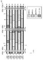
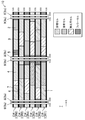
- FIG. 3 is a plan view showing a layout structure of the semiconductor integrated circuit device according to the first embodiment.
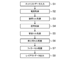
- 6 is a flowchart showing a design procedure of a semiconductor integrated circuit device.
- FIG. 3 is a plan view showing the layout structure of the semiconductor integrated circuit device after execution of step S2 in the first embodiment.
- FIG. 3 is a plan view showing the layout structure of the semiconductor integrated circuit device after execution of step S3 in the first embodiment.
- FIG. 6 is a plan view showing the layout structure of the semiconductor integrated circuit device after execution of step S5 in the first embodiment.
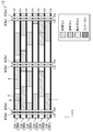
- FIG. 6 is a plan view showing a layout structure of a semiconductor integrated circuit device according to a second embodiment.
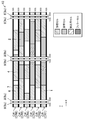
- FIG. 9 is a plan view showing the layout structure of the semiconductor integrated circuit device after execution of step S5 in the second embodiment.
- the semiconductor integrated circuit device includes a plurality of standard cells (hereinafter also simply referred to as cells).
- FIG. 1 is a circuit diagram showing a configuration example of a decoupling capacitance cell
- FIGS. 2A and 2B are circuit diagrams showing a configuration example of a correction cell. 1 and 2, the configuration is illustrated by circuit symbols, but in practice, a layout including diffusion regions, gate wirings, metal wirings, and the like is formed.
- Decoupling capacitance cell is a standard cell that is provided to suppress power supply voltage drop and power supply noise in semiconductor integrated circuit devices.
- the decoupling capacitance cell is configured by using a P-type MOS (Metal Oxide Semiconductor) transistor (PMOS) and an N-type MOS transistor (NMOS).
- PMOS Metal Oxide Semiconductor
- NMOS N-type MOS transistor
- P-type and N-type MOS transistors one of the power supplies VDD and VSS is connected to the drain and the source of each, and the power of opposite polarity is applied to the gate. Is composed of.
- VDD and VSS represent a power supply and a voltage supplied from the power supply.
- a decoupling capacity cell circuit 21 is configured in the decoupling capacity cell.
- the decoupling capacitance cell circuit 21 includes a fixed value output unit 22 and a decoupling capacitance unit 23.
- the fixed value output unit 22 includes a P-type transistor P1 and an N-type transistor N1.
- the decoupling capacitance unit 23 includes a P-type transistor P2 and an N-type transistor N2.
- the P-type transistor P1 has a source connected to the power supply VDD, a gate connected to the gate of the P-type transistor P2 and the drain of the N-type transistor N1, and a drain connected to the gate of the N-type transistor N1 and the gate of the N-type transistor N2. ..
- the N-type transistor N1 has a source connected to the power supply VSS.
- the P-type transistor P2 has its source and drain connected to the power supply VDD. The drain and the source of the N-type transistor N2 are connected to the power supply VSS, respectively.
- the fixed value output unit 22 always applies the voltages VSS and VDD to the gates of the P-type transistor P2 and the N-type transistor N2, respectively.
- the P-type transistor P2 and the N-type transistor N2 are always turned on, and the gate oxide film portions of the P-type transistor P2 and the N-type transistor N2 function as capacitors.
- the fixed value output unit 22 may not be provided in the decoupling capacitance cell circuit 21.
- the gate of the P-type transistor P2 and the gate of the N-type transistor N2 are directly connected to the power supplies VSS and VDD, respectively.
- the decoupling capacitance cell may be configured to use the capacitance between wirings without using a transistor.
- the “correction cell” is a standard cell that is used when an operation defect or function addition occurs after the cell placement and routing in the logic block is performed.
- the correction cell has a correction cell circuit 31.
- the correction cell circuit 31 includes a P-type transistor P3 and an N-type transistor N3.
- the source of the P-type transistor P3 is connected to the power supply VDD, the gate is connected to the gates of the input terminal A and the N-type transistor N3, and the drain is connected to the output terminal Y and the drain of the N-type transistor N3, respectively.
- the source of the N-type transistor N3 is connected to the power supply VSS. That is, the correction cell circuit 31 is an inverter circuit that inverts the signal input to the input terminal A and outputs the inverted signal from the output terminal Y.
- the power supply VSS is connected to the input terminal A and the output terminal Y is not connected in advance.
- the power supply VSS is disconnected from the input terminal A and the input terminal A and the output terminal Y are connected to other circuits.
- the semiconductor integrated circuit device can be modified into a desired circuit.
- the logic circuit configured in the correction cell may be a logic circuit other than the correction cell circuit 31 functioning as an inverter circuit, or may not be a logic circuit having a specific function.
- a repairing cell circuit 32 may be configured in which the repairing cell includes a P-type transistor P4 and an N-type transistor N4.
- the P-type transistor P4 the gate is connected to the terminal A1, the source is connected to the terminal Y1, and the drain is connected to the terminal Y2.
- the N-type transistor N4 has a gate connected to the terminal A2, a source connected to the terminal Y3, and a drain connected to the terminal Y4.
- the terminals A1, A2, Y1 to Y4 are not connected in advance, and when the semiconductor integrated circuit device is corrected, the terminals A1, A2, Y1 to Y4 form a desired circuit.
- the correction is realized by connecting to.
- FIG. 3 is a plan view showing the configuration of the semiconductor integrated circuit device according to the first embodiment, and shows a simplified layout pattern in a circuit block in which a capacitance cell and a correction cell are arranged (plan views below). The same).
- a semiconductor integrated circuit device 10 shown in FIG. 3 has a plurality of standard cells 1 arranged on a substrate. Further, the standard cell row CR including the plurality of standard cells 1 arranged side by side in the X direction (horizontal direction in the drawing, first direction) is arranged in the Y direction (vertical direction in the drawing, second direction perpendicular to the first direction). Are arranged in a plurality of rows (6 rows in FIG. 3).
- the standard cell 1 is, for example, a basic circuit element having a function such as an inverter or a logic circuit. By combining and arranging standard cells, a semiconductor integrated circuit device that realizes a predetermined function can be designed and manufactured. ..
- the standard cell row CR is arranged in the order of the standard cell rows CR1 to CR6 from the lower part of the drawing to the upper part of the drawing.
- the standard cell rows CR (CR1, CR3, CR5) arranged at odd-numbered positions from the bottom of the drawing are set as odd-numbered standard cell rows CR and are arranged at even-numbered positions from the bottom of the drawing.
- the standard cell row CR (CR2, CR4, CR6) is an even-numbered standard cell row CR.
- the power supply wiring 6 supplies the power supply potential VDD to the standard cell columns CR on both sides in the Y direction. Further, the power supply wiring 7 supplies the power supply potential VSS to the standard cell columns CR on both sides in the Y direction.
- the semiconductor integrated circuit device 10 is provided with strap power supply wirings 8 and 9 arranged above the power supply wirings 6 and 7 so as to extend in the Y direction.
- the strap power supply wiring 8 is connected to the power supply wiring 6 via a contact, and supplies the power supply potential VDD to the standard cell 1 arranged therebelow.
- the strap power supply wiring 9 is connected to the power supply wiring 7 via a contact and supplies the power supply potential VSS to the standard cell 1 arranged below the strap power supply wiring 9.
- FIG. 3 the contact between the power supply wiring 6 and the strap power supply wiring 8 and the contact between the power supply wiring 7 and the strap power supply wiring 9 are omitted.
- the strap power supply wirings 8 and 9 are alternately arranged in the X direction.
- the strap power supply wirings 8 (8a, 8b, 8c) are arranged at equal pitches
- the strap power supply wirings 9 (9a, 9b, 9c) are arranged at equal pitches.
- the strap power supply wirings 8a and 9a, the strap power supply wirings 8b and 9b, and the strap power supply wirings 8c and 9c are arranged adjacent to each other.
- the strap power supply wiring that supplies the power supply potential VDD and the strap power supply wiring that supplies the power supply potential VSS do not have to be arranged adjacent to each other.
- the standard cell 1 arranged in the standard cell column CR includes a capacity cell 2, a correction cell 3, a logic cell 4, and a filler cell 5.
- the capacitance cell 2 is a standard cell provided to suppress the power supply voltage drop and power supply noise in the semiconductor integrated circuit device 10. As shown in FIG. 3, the capacitance cell 2 includes a plurality of types of capacitance cells having different dimensions in the X direction.
- the correction cell 3 is a standard cell that is used when an operation defect or function addition occurs after the cell placement and routing in the logic block is performed. As shown in FIG. 3, the correction cell 3 includes a plurality of types of correction cells having different X-direction dimensions. The size of each correction cell 3 in the X direction differs depending on the logic circuit contained therein.
- the logic cell 4 is a standard cell arranged on the substrate to realize a desired circuit.
- the logic cell 4 is composed of, for example, a P-type transistor or an N-type transistor, and each has a predetermined logic function.
- the filler cell 5 is a standard cell that has no logic function, does not contribute to the logic function of the circuit block, and is arranged to fill a gap generated between the logic cell, the capacity cell, and the correction cell. ..
- the filler cell 5 may include a transistor (dummy transistor) having no logic function.
- FIG. 4 is a flowchart showing a method for designing a semiconductor integrated circuit device.
- 5 to 7 are plan views showing the layout structure of the semiconductor integrated circuit device after execution of step S2, step S3 and step S5 in the flow of FIG. 4, respectively.
- a device that outputs layout data of the semiconductor integrated circuit device that realizes a desired circuit based on the input netlist data for example, a computer for designing the semiconductor integrated circuit device is used.
- step S1 the netlist data describing the logic cells 4 forming a desired circuit and the connections between the logic cells 4 is input to the design computer.
- step S2 the power supply wirings 6 and 7 are arranged on the layout data board. As shown in FIG. 5, power supply wirings 6 and 7 extending in the X direction are alternately arranged in the Y direction. The power supply wirings 6 and 7 are arranged at intervals such that the standard cell row CR can be arranged between the power supply wirings 6 and 7 adjacent to each other in the Y direction.
- strap power supply wires 8 and 9 extending in the Y direction are alternately arranged in the X direction on the upper layers of the power supply wires 6 and 7.
- strap power supply wirings 8a and 9a are arranged on the left side of the drawing
- strap power supply wirings 8b and 9b are arranged on the center of the drawing
- strap power supply wirings 8c and 9c are arranged on the right side of the drawing, respectively.
- the strap power supply wirings 8a to 8c are connected to the power supply wiring 6 via contacts
- the strap power supply wirings 9a to 9c are connected to the power supply wiring 7 via contacts. ..
- step S3 the logic cell 4 is arranged on the board based on the netlist data. As shown in FIG. 6, the logic cells 4 are arranged in the standard cell columns CR1 to CR6 so as to realize a desired circuit configuration included in the netlist data.
- step S4 signal wiring is performed based on the netlist data. Although illustration is omitted, signal wiring is performed between the logic cells 4 arranged on the substrate based on the netlist data.
- step S5 the capacity cell 2 is arranged.
- the capacity cells 2 are arranged in this empty area.
- the capacity cells 2 are arranged only in the empty areas of the standard cell rows CR1, CR3, CR5 which are the odd-numbered standard cell rows CR. That is, the capacity cells 2 are arranged every other row in the standard cell row CR arranged side by side in the Y direction. The capacity cells 2 are arranged as much as possible in the empty areas of the odd-numbered standard cell rows CR.
- step S6 the correction cell 3 is placed.
- the standard cell column CR there is a free area (white portions in the standard cell columns CR1 to CR6) in which the capacitance cells 2 and the logic cells 4 are not arranged.
- the correction cell 3 is arranged in this empty area.
- the correction cell 3 is arranged in the empty area of the standard cell row CR2, CR4, CR6, which is the even-numbered standard cell row CR, in which the logic cell 4 is not arranged. That is, the correction cells 3 are arranged only in the even-numbered standard cell rows CR2, CR4, CR6 in which the capacity cells 2 are not arranged. Therefore, the correction cells 3 are arranged every other row in the standard cell row CR arranged side by side in the Y direction.
- the correction cells 3 are arranged as much as possible in the empty areas of the standard cell rows CR of even rows.
- step S7 the filler cell 5 is arranged.
- the capacitance cell 2, the correction cell 3, the logic cell 4 and the filler cell 5 are arranged on the substrate, a layout structure as shown in FIG. 3 is obtained.
- the filler cell 5 is arranged in an empty area of the standard cell column CR in which none of the capacity cell 2, the correction cell 3 and the logic cell 4 is arranged.
- the filler cell 5 is arranged in a very small empty area of the standard cell row CR in which none of the capacity cell 2, the correction cell 3 and the logic cell 4 can be arranged.
- step S8 the layout data of the semiconductor integrated circuit device 10 in which the capacity cell 2, the correction cell 3, the logic cell 4 and the filler cell 5 are arranged is output from the design computer.
- capacitance cells are provided between the strap power supply wirings 8a and 9a and the strap power supply wirings 8b and 9b and between the strap power supply wirings 8b and 9b and the strap power supply wirings 8c and 9c which are adjacent to each other in the X direction.
- 2 is arranged in the odd-numbered standard cell row CR (CR1, CR3, CR5)
- the correction cell 3 is arranged in the even-numbered standard cell row CR (CR2, CR4, CR6). That is, the standard cell row CR (CR1, CR3, CR5) in which only the capacitance cell 2 of the capacitance cell 2 and the correction cell 3 is arranged, and only the capacitance cell 2 of the capacitance cell 2 and the correction cell 3 is arranged.
- the standard cell rows CR (CR2, CR4, CR6) are alternately arranged in the Y direction.
- the capacitance cells 2 and the correction cells 3 are alternately arranged in the standard cell row CR arranged side by side in the Y direction, so that the capacitance cells 2 and the correction cells 3 arranged in the semiconductor integrated circuit device 10 are arranged. It is possible to surely arrange the capacitance cell 2 and the correction cell 3 in the semiconductor integrated circuit device 10 while suppressing the number of cells.
- the capacitance cell 2 is arranged between the adjacent power supply wirings 6 and 7 and connected to the power supply wirings 6 and 7.
- the capacity cells 2 are arranged every other row in the standard cell row CR arranged side by side in the Y direction. That is, both power supply wirings 6 and 7 are connected to the capacitance cell 2. As a result, it is possible to suppress the occurrence of local power supply voltage drop and power supply noise in the circuit block.
- correction cells 3 are arranged every other row in the standard cell row CR arranged side by side in the Y direction. As a result, there is a high possibility that the repair cell will be placed in the vicinity of the portion where the malfunction or the function is desired to be added, and the wiring delay due to the wiring to the repair cell can be suppressed.
- the capacity cell 2 is arranged in the odd standard cell row CR and the correction cell 3 is arranged in the even standard cell row CR, but not limited to this.
- the capacity cells 2 may be arranged in the even-numbered standard cell rows CR, and the correction cells 3 may be arranged in the odd-numbered standard cell rows CR.
- FIG. 8 is a plan view showing the configuration of the semiconductor integrated circuit device according to the second embodiment.
- the arrangement of the standard cell columns CR1 to CR6, the power supply lines 6 and 7, the strap power supply lines 8 and 9, and the logic cell 4 are the same as those in FIG.
- the capacitance cells 2 are odd-numbered standard cells between the strap power supply wirings 8a and 9a and the strap power supply wirings 8b and 9b, and between the strap power supply wirings 8b and 9b and the strap power supply wirings 8c and 9c.
- the correction cells 3 are arranged in the column CR, and the correction cells 3 are arranged in the even-numbered standard cell column CR. That is, the capacitance cell 2 and the correction cell 3 are the same between the strap power supply wirings 8a and 9a and the strap power supply wirings 8b and 9b and between the strap power supply wirings 8b and 9b and the strap power supply wirings 8c and 9c, respectively. It is arranged by the arrangement method.
- the capacitance cell 2 and the correction cell are arranged by different arrangement methods.
- the capacitor cells 2 are arranged in odd-numbered standard cell rows CR (CR1, CR3, CR5) between the strap power supply wirings 8a and 9a and the strap power supply wirings 8b and 9b, and the strap power supply wirings are provided. Between the 8b and 9b and the strap power supply wirings 8c and 9c, the standard cell columns CR (CR2, CR4, CR6) of even columns are arranged.
- the correction cells 3 are arranged in the even-numbered standard cell rows CR (CR2, CR4, CR6) between the strap power supply wirings 8a and 9a and the strap power supply wirings 8b and 9b, and the strap power supply wirings 8b and 9b. And the strap power supply wirings 8c and 9c are arranged in the odd-numbered standard cell column CR.
- FIG. 9 shows a layout structure of the semiconductor integrated circuit device after execution of step S5.
- steps S1 to S4, S7, and S8 are the same as those in the first embodiment, so description thereof will be omitted.
- step S5 the capacity cell 2 is arranged.
- the odd standard cell rows CR (CR1, CR3, CR5) are vacant.
- the strap power supply wirings 8b and 9b and the strap power supply wirings 8c and 9c are arranged in the empty areas of the even-numbered standard cell rows CR (CR2, CR4, CR6). That is, between the strap power supply wirings 8a and 9a and the strap power supply wirings 8c and 9c, the capacitance cells 2 are arranged on both sides of the power supply wirings 6 and 7 in the Y direction.
- step S6 the correction cell 3 is placed.
- the correction cell 3 has an empty even number of standard cell rows CR (CR2, CR4, CR6) between the strap power supply wirings 8a and 9a and the strap power supply wirings 8b and 9b. It is arranged in a region, and is arranged in an empty region of the odd-numbered standard cell row CR (CR1, CR3, CR5) between the strap power supply wirings 8b and 9b and the strap power supply wirings 8c and 9c.
- the power supply wiring 6 when power supply noise is generated in the power supply wiring 6 arranged between the standard cell rows CR3 and CR4, the power supply wiring 6 is arranged on both sides of the power supply wiring 6 via the capacitance cell 2 connected to the power supply wiring 6.
- Power supply noise propagates to the power supply wiring 7 (the power supply wiring 7 arranged between the standard cell rows CR2 and CR3 and the power supply wiring 7 arranged between the standard cell rows CR4 and CR5). That is, when power supply noise occurs in any of the power supply wirings 6 and 7, the power supply noise propagates to the power supply wirings 6 and 7 arranged on both sides via the capacitive cell 2. As a result, the power supply noise generated in the power supply lines 6 and 7 is dispersed, so that the influence of the power supply noise can be reduced.
- the capacity cell 2 and the correction cell 3 may be arranged in reverse.
- the capacitance cells 2 are arranged in the odd-numbered standard cell rows CR between the strap power supply wirings 8a and 9a and the strap power supply wirings 8b and 9b, and the strap power supply wirings 8b and 9b and the strap power supply wiring 8c, Between 9c and 9c, they are arranged in the even-numbered standard cell column CR.
- correction cells 3 are arranged in the even-numbered standard cell rows CR between the strap power supply wirings 8a and 9a and the strap power supply wirings 8b and 9b, and the strap power supply wirings 8b and 9b and the strap power supply wiring 8c, Between 9c and 9c, they are arranged in odd-numbered standard cell columns CR.
- the correction cell 3 is arranged after the capacity cell 2 is arranged.
- the present invention is not limited to this, and the capacity cell 2 is arranged after the correction cell 3 is arranged. May be.
- the number of standard cell rows arranged side by side in the Y direction is six, but the number is not limited to this, and the number of standard cell rows may be two or more.
- the decoupling capacitance cell and the correction cell can be arranged while suppressing the area of the semiconductor integrated circuit device.
Landscapes
- Design And Manufacture Of Integrated Circuits (AREA)
- Semiconductor Integrated Circuits (AREA)
- Engineering & Computer Science (AREA)
- General Engineering & Computer Science (AREA)
- Power Engineering (AREA)
Abstract
電源電位VDDを供給するストラップ電源配線(8a,8b)の間において、容量セル(2)および修正用セル(3)のうち容量セル(2)のみが配置されたスタンダードセル列(CR1,CR3,CR5)と、容量セル(2)および修正用セル(3)のうち修正用セル(3)のみが配置されたスタンダードセル列(CR2,CR4,CR6)とが、Y方向において、交互に配置される。
Description
本開示は、スタンダードセルを備えた半導体集積回路装置、特にスタンダードセルとしてデカップリング容量セルおよび修正用セルを備えた半導体集積回路装置に関するものである。
半導体基板上に半導体集積回路を形成する方法として、スタンダードセル方式が知られている。スタンダードセル方式とは、特定の論理機能を有する基本的単位(例えば、インバータ,ラッチ,フリップフロップ,全加算器など)をスタンダードセルとして予め用意しておき、半導体基板上に複数のスタンダードセルを配置して、それらのスタンダードセルを配線で接続することによって、LSIチップを設計する方式のことである。
また、近年、LSIの大規模化、高速化、低電圧化に伴い、電源電圧降下や電源ノイズの影響が大きくなってきており、これらを抑制するためのスタンダードセルとしてデカップリング容量セルが半導体集積回路装置内に配置される。
また、半導体集積回路装置の設計後に動作不具合や機能追加への対応をより少ないマスクの修正(たとえば一部のメタル配線層のマスクの修正)によって可能とするためのスタンダードセルとして、修正用セルが半導体集積回路装置内に配置される。
特許文献1では、複数のスタンダードセル列で構成された半導体集積回路装置において、デカップリング容量セル(以下、適宜、単に容量セルともいう)と修正用セルとが複数のセル列に配置された半導体集積回路装置およびその設計方法が開示されている。
ところで、特許文献1では、デカップリング容量セルおよび修正用セルの配置順については開示されているが、デカップリング容量セルおよび修正用セルの配置パターンについては開示されていない。
スタンダードセルで構成された半導体集積回路装置において、各スタンダードセル列に含まれる電源配線に生じる電源電圧降下や電源ノイズを抑制するために、電源配線ごとにデカップリング容量セルを備える方が好ましい。また、修正用セルに対する配線による配線遅延を抑制するために、動作不具合や機能追加を行いたい部分の近傍に修正用セルを備える方が好ましい。しかし、これらを満たすためには、多数のデカップリング容量セルおよび修正用セルを半導体集積回路装置に備える必要があり、半導体集積回路装置の面積が大きくなる。
本開示は、これらの課題を解決する、修正用セルおよびデカップリング容量セルを用いた半導体集積回路装置を提供する。
本開示では、第1方向に延びる複数の電源配線と、前記第1方向に並ぶ複数のスタンダードセルをそれぞれ備え、前記電源配線同士の間にそれぞれ配置された、複数のセル列と、前記複数のセル列の上方において、前記第1方向と垂直をなす第2方向に延びており、前記第1方向において離間して隣り合う、同一電源電圧を供給する第1および第2ストラップ電源配線とを備え、前記複数の電源配線は、第1電源電圧を供給する第1電源配線、および、前記第1電源電圧と異なる第2電源電圧を供給する第2電源配線を含み、前記第1電源配線と前記第2電源配線とは、前記第2方向において交互に配置されており、前記複数のセル列は、前記第1ストラップ電源配線と前記第2ストラップ電源配線との間の第1領域において、容量セルおよび修正用セルのうち容量セルのみが配置された第1セル列と、前記第1領域において容量セルおよび修正用セルのうち修正用セルのみが配置された第2セル列とを含み、前記第1セル列と前記第2セル列とは、前記第2方向において交互に配置されている。
この態様によると、複数のセル列は、第1ストラップ電源配線と第2ストラップ電源配線との間の第1領域において、容量セルおよび修正用セルのうち容量セルのみが配置された第1セル列と、第1領域において容量セルおよび修正用セルのうち修正用セルのみが配置された第2セル列とを含む。第1セル列と第2セル列とは、第2方向において、交互に配置される。すなわち、容量セルおよび修正用セルは、第2方向に並んで配置されたセル列において、交互に配置される。これにより、半導体集積回路装置に配置される容量セルおよび修正用セルの数を抑えつつ、容量セルおよび修正用セルを半導体集積回路装置に確実に配置することができる。
また、容量セルが配置された第1セル列は、第2方向において、一列おきに配置される。これにより、いずれの電源配線も容量セルと接続されるため、回路ブロック内の局所的な電源電圧降下や電源ノイズの発生を抑制することができる。
また、修正用セルが配置された第2セル列は、第2方向において、一列おきに配置される。これにより、動作不具合や機能追加を行いたい部分の近傍に修正用セルが配置される可能性が高くなり、修正用セルに対する配線による配線遅延を抑制することができる。
本開示によると、半導体集積回路装置の面積を抑えつつ、電源配線に生じる電源効果や電源ノイズを抑制し、かつ、修正用セルに対する配線遅延を抑制することができる。
以下、実施の形態について、図面を参照して説明する。以下の実施の形態では、半導体集積回路装置は複数のスタンダードセル(以下、適宜、単にセルともいう)を備える。
まず、デカップリング容量セル(以下、適宜、単に容量セルともいう)および修正用セルについて説明する。図1はデカップリング容量セルの構成例を示す回路図であり、図2(a),(b)は修正用セルの構成例を示す回路図である。なお、図1および図2では、構成を回路記号によって図示しているが、実際には、拡散領域やゲート配線、メタル配線等からなるレイアウトが形成される。
「デカップリング容量セル」は、半導体集積回路装置内の電源電圧降下や電源ノイズを抑制するために設けられるスタンダードセルである。デカップリング容量セルは、P型MOS(Metal Oxide Semiconductor)トランジスタ(PMOS)およびN型MOSトランジスタ(NMOS)を用いて構成される。P型およびN型MOSトランジスタ(以下、単にP型およびN型トランジスタという)は、それぞれのドレインおよびソースに電源VDD,VSSのいずれか一方が接続され、ゲートに逆極性の電源が印加されるように構成される。なお、本明細書において、VDD,VSSは、電源および電源から供給される電圧を示すものとする。
図1に示すように、デカップリング容量セルには、デカップリング容量セル回路21が構成されている。デカップリング容量セル回路21は、固定値出力部22と、デカップリング容量部23とを備える。
固定値出力部22は、P型トランジスタP1と、N型トランジスタN1とを備える。デカップリング容量部23は、P型トランジスタP2と、N型トランジスタN2とを備える。P型トランジスタP1は、ソースが電源VDDに、ゲートがP型トランジスタP2のゲートおよびN型トランジスタN1のドレインに、ドレインがN型トランジスタN1のゲートおよびN型トランジスタN2のゲートにそれぞれ接続されている。N型トランジスタN1は、ソースが電源VSSに接続されている。P型トランジスタP2は、ソースおよびドレインがそれぞれ電源VDDに接続されている。N型トランジスタN2は、ドレインおよびソースがそれぞれ電源VSSに接続されている。また、固定値出力部22により、P型トランジスタP2およびN型トランジスタN2のゲートには、それぞれ、電圧VSS,VDDが常に印加される。これにより、P型トランジスタP2およびN型トランジスタN2が常にオン状態となり、P型トランジスタP2およびN型トランジスタN2のゲート酸化膜部分が容量として機能する。
なお、デカップリング容量セル回路21に固定値出力部22が設けられていなくてもよい。この場合、P型トランジスタP2のゲート、および、N型トランジスタN2のゲートが、それぞれ、電源VSS,VDDに直接接続される。また、デカップリング容量セルは、トランジスタを用いずに、配線間容量を利用した構成であってもよい。
「修正用セル」は、論理ブロックにおけるセル配置配線が実施された後、動作不具合や機能追加が発生した場合に使用されるスタンダードセルである。
図2(a)に示すように、修正用セルには、修正用セル回路31が構成されている。修正用セル回路31は、P型トランジスタP3と、N型トランジスタN3とを備える。
P型トランジスタP3は、ソースが電源VDDに、ゲートが入力端子AおよびN型トランジスタN3のゲートに、ドレインが出力端子YおよびN型トランジスタN3のドレインに、それぞれ接続されている。N型トランジスタN3は、ソースが電源VSSに接続されている。すなわち、修正用セル回路31は、入力端子Aに入力された信号を反転して出力端子Yから出力するインバータ回路である。
図2(a)に示すように、修正用セル回路31では、予め、入力端子Aに電源VSSを接続しておき、出力端子Yを未接続にしておく。そして、半導体集積回路装置の修正時に、インバータ回路の追加が必要となるとき、入力端子Aから電源VSSを切り離して、入力端子Aおよび出力端子Yを他の回路に接続する。これにより、半導体集積回路装置を所望の回路に修正することができる。
また、修正用セルに構成される論理回路は、インバータ回路として機能する修正用セル回路31以外の論理回路であってもよいし、特定の機能を持った論理回路でなくてもよい。例えば、図2(b)に示すように、修正用セルにP型トランジスタP4およびN型トランジスタN4を備える修正用セル回路32を構成してもよい。P型トランジスタP4は、ゲートが端子A1に、ソースが端子Y1に、ドレインが端子Y2にそれぞれ接続されている。N型トランジスタN4は、ゲートが端子A2に、ソースが端子Y3に、ドレインが端子Y4にそれぞれ接続されている。修正用セル回路32では、予め、端子A1,A2,Y1~Y4を未接続にしておき、半導体集積回路装置を修正するときに、端子A1,A2,Y1~Y4を所望の回路を構成するように接続することで修正を実現する。
(第1実施形態)
次に、第1実施形態に係る半導体集積回路装置の構造を説明する。
次に、第1実施形態に係る半導体集積回路装置の構造を説明する。
図3は第1実施形態に係る半導体集積回路装置の構成を示す平面図であり、容量セルおよび修正用セルが配置された回路ブロックにおけるレイアウトパターンを簡略化して図示している(以降の平面図も同様)。図3に示す半導体集積回路装置10は、基板に、複数のスタンダードセル1が配置されている。また、X方向(図面横方向、第1方向)に並べて配置された複数のスタンダードセル1を備えたスタンダードセル列CRが、Y方向(図面縦方向、第1方向と垂直をなす第2方向)に複数列(図3では、6列)配置されている。スタンダードセル1は、例えばインバータや論理回路等の機能を有する基本回路素子であり、スタンダードセルを組み合わせて配置配線することによって、所定の機能を実現する半導体集積回路装置を設計・製造することができる。
スタンダードセル列CRは、図面下部から図面上部にかけて、スタンダードセル列CR1~CR6の順で配置されている。なお、図3等において、図面下部から数えて奇数番目に配置されたスタンダードセル列CR(CR1,CR3,CR5)を奇数列のスタンダードセル列CRとし、図面下部から数えて偶数番目に配置されたスタンダードセル列CR(CR2,CR4,CR6)を偶数列のスタンダードセル列CRとする。
スタンダードセル列CR同士の間に、スタンダードセル1に電源電位VDDを供給する電源配線6(右横にVDDと記す)と、スタンダードセル1に電源電位VSSを供給する電源配線7(右横にVSSと記す)とが、交互に、配置されている。電源配線6,7はともに、X方向に延びるように配置されている。電源配線6は、そのY方向両側のスタンダードセル列CRに電源電位VDDを供給する。また、電源配線7は、そのY方向両側のスタンダードセル列CRに電源電位VSSを供給する。
半導体集積回路装置10には、電源配線6,7の上層に、Y方向に延びるように配置されたストラップ電源配線8,9が設けられている。ストラップ電源配線8は、コンタクトを介して電源配線6と接続されており、その下方に配置されたスタンダードセル1に電源電位VDDを供給する。また、ストラップ電源配線9は、コンタクトを介して電源配線7と接続されており、その下方に配置されたスタンダードセル1に電源電位VSSを供給する。なお、図3では、電源配線6とストラップ電源配線8とのコンタクト、および、電源配線7とストラップ電源配線9とのコンタクトについては、省略して図示している。
図3に示すように、ストラップ電源配線8,9は、X方向において、交互に、配置されている。例えば、ストラップ電源配線8(8a,8b,8c)は、等ピッチで離間して配置されており、ストラップ電源配線9(9a,9b,9c)は、等ピッチで離間して配置されている。
また、図3では、ストラップ電源配線8a,9a、ストラップ電源配線8b,9b、および、ストラップ電源配線8c,9cは、それぞれ、互いに隣接して配置されている。ただし、電源電位VDDを供給するストラップ電源配線と、電源電位VSSを供給するストラップ電源配線とは、隣接して配置されなくてもよい。
また、スタンダードセル列CRに配置されるスタンダードセル1には、容量セル2と、修正用セル3と、論理セル4と、フィラーセル5とが含まれる。
容量セル2は、上述したとおり、半導体集積回路装置10内の電源電圧降下や電源ノイズを抑制するために設けられるスタンダードセルである。図3に示すように、容量セル2には、X方向の寸法が異なる複数種類の容量セルが含まれる。
修正用セル3は、上述したとおり、論理ブロックにおけるセル配置配線が実施された後、動作不具合や機能追加が発生した場合に使用されるスタンダードセルである。図3に示すように、修正用セル3には、X方向の寸法が異なる複数種類の修正用セルが含まれる。各修正用セル3は、それぞれの内部に含まれる論理回路によって、X方向の寸法が異なる。
論理セル4は、所望の回路を実現するために基板上に配置されるスタンダードセルである。論理セル4は、例えば、P型トランジスタやN型トランジスタ等で構成され、それぞれが所定の論理機能を有する。
フィラーセル5は、論理機能を有しておらず、回路ブロックの論理機能に寄与せず、論理セル、容量セル、修正用セルの間に生じた隙間を埋めるために配置されたスタンダードセルである。フィラーセル5は、論理機能を有さないトランジスタ(ダミートランジスタ)が含まれることがある。
次に、図3~図7を参照しながら、第1実施形態に係る半導体集積回路装置の設計方法を説明する。
図4は半導体集積回路装置の設計方法を示すフローチャートである。図5~図7は、それぞれ、図4のフローにおけるステップS2、ステップS3およびステップS5実行後の半導体集積回路装置のレイアウト構造を示す平面図である。
半導体集積回路装置の設計には、入力されたネットリストデータに基づき、所望の回路を実現する半導体集積回路装置のレイアウトデータを出力する装置、例えば、半導体集積回路装置の設計用コンピュータが用いられる。
具体的には、ステップS1において、所望の回路を構成する論理セル4と、論理セル4間の接続とを記載したネットリストデータを設計用コンピュータに入力する。
ステップS2において、レイアウトデータの基板上に電源配線6,7が配置される。図5に示すように、X方向に延びる電源配線6,7が、Y方向において、交互に配置される。電源配線6,7は、それぞれ、Y方向に隣接する電源配線6,7との間にスタンダードセル列CRが配置可能な間隔を空けて配置される。
また、電源配線6,7の上層には、Y方向に延びるストラップ電源配線8,9がX方向に交互に配置される。図5に示すように、図面左側にストラップ電源配線8a,9aが、図面中央にストラップ電源配線8b,9bが、図面右側にストラップ電源配線8c,9cが、それぞれ、配置される。また、図示は省略するが、ストラップ電源配線8a~8cは、それぞれ、コンタクトを介して電源配線6と接続され、ストラップ電源配線9a~9cは、それぞれ、コンタクトを介して電源配線7と接続される。
ステップS3において、ネットリストデータに基づいて、基板上に論理セル4が配置される。図6に示すように、論理セル4は、ネットリストデータに含まれる所望の回路構成を実現するように、スタンダードセル列CR1~CR6に配置される。
ステップS4において、ネットリストデータに基づいて、信号配線が行われる。図示は省略するが、ネットリストデータに基づき、基板上に配置された論理セル4間の信号配線が行われる。
ステップS5において、容量セル2が配置される。図6に示すように、スタンダードセル列CRには、論理セル4が配置されていない空き領域(スタンダードセル列CR1~CR6における白色部分)が存在する。この空き領域に容量セル2が配置される。図7に示すように、容量セル2は、奇数列のスタンダードセル列CRであるスタンダードセル列CR1,CR3,CR5の空き領域にのみ配置される。すなわち、容量セル2は、Y方向に並べて配置されたスタンダードセル列CRにおいて、一列おきに配置される。なお、容量セル2は、奇数列のスタンダードセル列CRの空き領域に可能な限り配置される。
ステップS6において、修正用セル3が配置される。図7に示すように、スタンダードセル列CRには、容量セル2および論理セル4が配置されていない空き領域(スタンダードセル列CR1~CR6における白色部分)が存在する。この空き領域に修正用セル3が配置される。具体的には、修正用セル3は、偶数列のスタンダードセル列CRであるスタンダードセル列CR2,CR4,CR6の、論理セル4が配置されていない空き領域に配置される。すなわち、修正用セル3は、容量セル2が配置されていない偶数列のスタンダードセル列CR2,CR4,CR6にのみ配置される。このため、修正用セル3は、Y方向に並べて配置されたスタンダードセル列CRにおいて、一列おきに配置される。なお、修正用セル3は、偶数列のスタンダードセル列CRの空き領域に可能な限り配置される。
ステップS7において、フィラーセル5が配置される。容量セル2、修正用セル3、論理セル4およびフィラーセル5が基板上に配置されると、図3のようなレイアウト構造となる。フィラーセル5は、容量セル2、修正用セル3および論理セル4のいずれも配置されていないスタンダードセル列CRの空き領域に配置される。フィラーセル5は、容量セル2、修正用セル3および論理セル4のいずれも配置できないようなスタンダードセル列CRの極小の空き領域に配置される。
ステップS8において、設計用コンピュータから、容量セル2、修正用セル3、論理セル4およびフィラーセル5が配置された半導体集積回路装置10のレイアウトデータが出力される。
以上の構成により、X方向に隣り合う、ストラップ電源配線8a,9aとストラップ電源配線8b,9bとの間、および、ストラップ電源配線8b,9bとストラップ電源配線8c,9cとの間において、容量セル2は奇数列のスタンダードセル列CR(CR1,CR3,CR5)に配置され、修正用セル3は偶数列のスタンダードセル列CR(CR2,CR4,CR6)に配置される。すなわち、容量セル2および修正用セル3のうち容量セル2のみが配置されたスタンダードセル列CR(CR1,CR3,CR5)と、容量セル2および修正用セル3のうち容量セル2のみが配置されたスタンダードセル列CR(CR2,CR4,CR6)とが、Y方向において、交互に配置される。これにより、容量セル2および修正用セル3が、Y方向に並べて配置されたスタンダードセル列CRにおいて、交互に配置されるため、半導体集積回路装置10に配置される容量セル2および修正用セル3の数を抑えつつ、容量セル2および修正用セル3を確実に半導体集積回路装置10内に配置することができる。
また、容量セル2は、隣接する電源配線6,7の間に配置され、その電源配線6,7に接続される。また、容量セル2は、Y方向に並べて配置されたスタンダードセル列CRにおいて、一列おきに配置される。すなわち、いずれの電源配線6,7も容量セル2と接続されることになる。これにより、回路ブロック内の局所的な電源電圧降下や電源ノイズの発生を抑制することができる。
また、修正用セル3は、Y方向に並べて配置されたスタンダードセル列CRにおいて、一列おきに配置される。これにより、動作不具合や機能追加を行いたい部分の近傍に修正用セルが配置される可能性が高くなり、修正用セルに対する配線による配線遅延を抑制することができる。
なお、容量セル2が奇数列のスタンダードセル列CRに配置され、修正用セル3が偶数列のスタンダードセル列CRに配置されているが、これに限られない。容量セル2が偶数列のスタンダードセル列CRに配置され、修正用セル3が奇数列のスタンダードセル列CRに配置されてもよい。
(第2実施形態)
図8は第2実施形態に係る半導体集積回路装置の構成を示す平面図である。スタンダードセル列CR1~CR6、電源配線6,7、ストラップ電源配線8,9、および、論理セル4の配置に関しては、図3と同様であるので、説明を省略する。
図8は第2実施形態に係る半導体集積回路装置の構成を示す平面図である。スタンダードセル列CR1~CR6、電源配線6,7、ストラップ電源配線8,9、および、論理セル4の配置に関しては、図3と同様であるので、説明を省略する。
図3では、ストラップ電源配線8a,9aとストラップ電源配線8b,9bとの間、および、ストラップ電源配線8b,9bとストラップ電源配線8c,9cとの間において、容量セル2は奇数列のスタンダードセル列CRに配置され、修正用セル3は偶数列のスタンダードセル列CRに配置されている。すなわち、ストラップ電源配線8a,9aとストラップ電源配線8b,9bとの間、ストラップ電源配線8b,9bとストラップ電源配線8c,9cとの間において、容量セル2および修正用セル3は、それぞれ、同じ配置方法で配置される。
これに対して、図8では、ストラップ電源配線8a,9aとストラップ電源配線8b,9bとの間、ストラップ電源配線8b,9bとストラップ電源配線8c,9cとの間において、容量セル2および修正用セル3は、それぞれ、異なる配置方法で配置される。
具体的には、容量セル2は、ストラップ電源配線8a,9aとストラップ電源配線8b,9bとの間においては、奇数列のスタンダードセル列CR(CR1,CR3,CR5)に配置され、ストラップ電源配線8b,9bとストラップ電源配線8c,9cとの間においては、偶数列のスタンダードセル列CR(CR2,CR4,CR6)に配置される。
また、修正用セル3は、ストラップ電源配線8a,9aとストラップ電源配線8b,9bとの間において、偶数列のスタンダードセル列CR(CR2,CR4,CR6)に配置され、ストラップ電源配線8b,9bとストラップ電源配線8c,9cとの間において、奇数列のスタンダードセル列CRに配置される。
次に、図4、図6、図8および図9を参照しながら、第2実施形態に係る半導体集積回路装置の設計方法について説明する。図9はステップS5実行後の半導体集積回路装置のレイアウト構造である。図4において、ステップS1~S4,S7,S8は第1実施形態と同様であるので、説明を省略する。
ステップS5において、容量セル2が配置される。図6および図9に示すように、容量セル2は、ストラップ電源配線8a,9aとストラップ電源配線8b,9bとの間においては、奇数列のスタンダードセル列CR(CR1,CR3,CR5)の空き領域に配置され、ストラップ電源配線8b,9bとストラップ電源配線8c,9cとの間においては、偶数列のスタンダードセル列CR(CR2,CR4,CR6)の空き領域に配置される。すなわち、ストラップ電源配線8a,9aとストラップ電源配線8c,9cとの間において、電源配線6,7それぞれのY方向両側には、容量セル2が配置される。
ステップS6において、修正用セル3が配置される。図8および図9に示すように、修正用セル3は、ストラップ電源配線8a,9aとストラップ電源配線8b,9bとの間において、偶数列のスタンダードセル列CR(CR2,CR4,CR6)の空き領域に配置され、ストラップ電源配線8b,9bとストラップ電源配線8c,9cとの間において、奇数列のスタンダードセル列CR(CR1,CR3,CR5)の空き領域に配置される。
図9の構成によって、図3と同様の効果を得ることができる。
また、例えば、スタンダードセル列CR3,CR4の間に配置された電源配線6において電源ノイズが発生した場合、電源配線6に接続された容量セル2を介して、電源配線6の両隣に配置された電源配線7(スタンダードセル列CR2,CR3の間に配置された電源配線7、および、スタンダードセル列CR4,CR5の間に配置された電源配線7)に電源ノイズが伝搬する。すなわち、電源配線6,7のいずれかで電源ノイズが発生した場合に、容量セル2を介して、両隣に配置された電源配線6,7に電源ノイズが伝搬する。これにより、電源配線6,7において発生した電源ノイズが分散されるので、電源ノイズの影響を低減することができる。
なお、容量セル2と修正用セル3とを逆に配置してもよい。この場合、容量セル2は、ストラップ電源配線8a,9aとストラップ電源配線8b,9bとの間においては、奇数列のスタンダードセル列CRに配置され、ストラップ電源配線8b,9bとストラップ電源配線8c,9cとの間においては、偶数列のスタンダードセル列CRに配置される。また、修正用セル3は、ストラップ電源配線8a,9aとストラップ電源配線8b,9bとの間においては、偶数列のスタンダードセル列CRに配置され、ストラップ電源配線8b,9bとストラップ電源配線8c,9cとの間においては、奇数列のスタンダードセル列CRに配置される。
なお、上記各実施形態では、容量セル2が配置された後、修正用セル3が配置されるとしたが、これに限られず、修正用セル3が配置された後、容量セル2が配置されてもよい。
また、上記各実施形態では、Y方向に並べて配置されるスタンダードセル列は6列としたが、これに限られず、スタンダードセル列は2列以上であればよい。
本開示では、スタンダードセルを備えた半導体集積回路装置について、デカップリング容量セルおよび修正用セルを、半導体集積回路装置の面積を抑えつつ、配置することができる。
1 スタンダードセル
2 デカップリング容量セル
3 修正用セル
6,7 電源配線
8,9(8a~8c,9a~9c) ストラップ電源配線
CR(CR1~CR6) スタンダードセル列
2 デカップリング容量セル
3 修正用セル
6,7 電源配線
8,9(8a~8c,9a~9c) ストラップ電源配線
CR(CR1~CR6) スタンダードセル列
Claims (3)
- 第1方向に延びる複数の電源配線と、
前記第1方向に並ぶ複数のスタンダードセルをそれぞれ備え、前記電源配線同士の間にそれぞれ配置された、複数のセル列と、
前記複数のセル列の上方において、前記第1方向と垂直をなす第2方向に延びており、前記第1方向において離間して隣り合う、同一電源電圧を供給する第1および第2ストラップ電源配線とを備え、
前記複数の電源配線は、第1電源電圧を供給する第1電源配線、および、前記第1電源電圧と異なる第2電源電圧を供給する第2電源配線を含み、前記第1電源配線と前記第2電源配線とは、前記第2方向において交互に配置されており、
前記複数のセル列は、前記第1ストラップ電源配線と前記第2ストラップ電源配線との間の第1領域において、容量セルおよび修正用セルのうち容量セルのみが配置された第1セル列と、前記第1領域において容量セルおよび修正用セルのうち修正用セルのみが配置された第2セル列とを含み、前記第1セル列と前記第2セル列とは、前記第2方向において交互に配置されていることを特徴とする半導体集積回路装置。 - 請求項1記載の半導体集積回路装置において、
前記複数のセル列の上方において前記第2方向に延びており、前記第1方向において前記第2ストラップ電源配線と、前記第1ストラップ電源配線と反対側に、離間して隣り合う、前記第1および第2ストラップ電源配線と同一電源電圧を供給する第3ストラップ電源配線を備え、
前記第2ストラップ電源配線と前記第3ストラップ電源配線との間の領域において、前記第1セル列は、容量セルおよび修正用セルのうち容量セルのみが配置されており、前記第2セル列は、容量セルおよび修正用セルのうち修正用セルのみが配置されていることを特徴とする半導体集積回路装置。 - 請求項1記載の半導体集積回路装置において、
前記複数のセル列の上方において前記第2方向に延びており、前記第1方向において前記第2ストラップ電源配線と、前記第1ストラップ電源配線と反対側に、離間して隣り合う、前記第1および第2ストラップ電源配線と同一電源電圧を供給する第3ストラップ電源配線を備え、
前記第2ストラップ電源配線と前記第3ストラップ電源配線との間の領域において、前記第1セル列は、容量セルおよび修正用セルのうち修正用セルのみが配置されており、前記第2セル列は、容量セルおよび修正用セルのうち容量セルのみが配置されている
ことを特徴とする半導体集積回路装置。
Priority Applications (3)
| Application Number | Priority Date | Filing Date | Title |
|---|---|---|---|
| JP2020565071A JP7157350B2 (ja) | 2019-01-09 | 2019-01-09 | 半導体集積回路装置 |
| PCT/JP2019/000367 WO2020144767A1 (ja) | 2019-01-09 | 2019-01-09 | 半導体集積回路装置 |
| US17/370,912 US20210335774A1 (en) | 2019-01-09 | 2021-07-08 | Semiconductor integrated circuit device |
Applications Claiming Priority (1)
| Application Number | Priority Date | Filing Date | Title |
|---|---|---|---|
| PCT/JP2019/000367 WO2020144767A1 (ja) | 2019-01-09 | 2019-01-09 | 半導体集積回路装置 |
Related Child Applications (1)
| Application Number | Title | Priority Date | Filing Date |
|---|---|---|---|
| US17/370,912 Continuation US20210335774A1 (en) | 2019-01-09 | 2021-07-08 | Semiconductor integrated circuit device |
Publications (1)
| Publication Number | Publication Date |
|---|---|
| WO2020144767A1 true WO2020144767A1 (ja) | 2020-07-16 |
Family
ID=71521516
Family Applications (1)
| Application Number | Title | Priority Date | Filing Date |
|---|---|---|---|
| PCT/JP2019/000367 Ceased WO2020144767A1 (ja) | 2019-01-09 | 2019-01-09 | 半導体集積回路装置 |
Country Status (3)
| Country | Link |
|---|---|
| US (1) | US20210335774A1 (ja) |
| JP (1) | JP7157350B2 (ja) |
| WO (1) | WO2020144767A1 (ja) |
Families Citing this family (2)
| Publication number | Priority date | Publication date | Assignee | Title |
|---|---|---|---|---|
| KR20230041877A (ko) * | 2021-09-17 | 2023-03-27 | 삼성전자주식회사 | 반도체 장치 및 그의 제조 방법 |
| US20250311438A1 (en) * | 2024-04-02 | 2025-10-02 | Samsung Electronics Co., Ltd. | Integrated circuit including high-power consumption cell and method of manufacturing the same |
Citations (9)
| Publication number | Priority date | Publication date | Assignee | Title |
|---|---|---|---|---|
| JP2001148464A (ja) * | 1999-11-18 | 2001-05-29 | Toshiba Microelectronics Corp | 半導体集積回路 |
| JP2001358221A (ja) * | 2000-06-14 | 2001-12-26 | Fujitsu Ltd | レイアウト方法、レイアウト装置及び記録媒体 |
| JP2002110798A (ja) * | 2000-09-27 | 2002-04-12 | Hitachi Ltd | 半導体装置およびそのレイアウト方法 |
| JP2005142226A (ja) * | 2003-11-04 | 2005-06-02 | Matsushita Electric Ind Co Ltd | 半導体集積回路およびその設計方法 |
| JP2007234857A (ja) * | 2006-03-01 | 2007-09-13 | Matsushita Electric Ind Co Ltd | 半導体集積回路および半導体集積回路の設計方法 |
| JP2008277788A (ja) * | 2007-04-05 | 2008-11-13 | Nec Electronics Corp | 半導体装置 |
| WO2013132841A1 (ja) * | 2012-03-08 | 2013-09-12 | パナソニック株式会社 | 半導体集積回路装置 |
| JP2016130919A (ja) * | 2015-01-13 | 2016-07-21 | 株式会社ソシオネクスト | 半導体装置の設計方法及び半導体装置の製造方法 |
| WO2017090389A1 (ja) * | 2015-11-25 | 2017-06-01 | 株式会社ソシオネクスト | 半導体集積回路装置 |
-
2019
- 2019-01-09 JP JP2020565071A patent/JP7157350B2/ja active Active
- 2019-01-09 WO PCT/JP2019/000367 patent/WO2020144767A1/ja not_active Ceased
-
2021
- 2021-07-08 US US17/370,912 patent/US20210335774A1/en not_active Abandoned
Patent Citations (9)
| Publication number | Priority date | Publication date | Assignee | Title |
|---|---|---|---|---|
| JP2001148464A (ja) * | 1999-11-18 | 2001-05-29 | Toshiba Microelectronics Corp | 半導体集積回路 |
| JP2001358221A (ja) * | 2000-06-14 | 2001-12-26 | Fujitsu Ltd | レイアウト方法、レイアウト装置及び記録媒体 |
| JP2002110798A (ja) * | 2000-09-27 | 2002-04-12 | Hitachi Ltd | 半導体装置およびそのレイアウト方法 |
| JP2005142226A (ja) * | 2003-11-04 | 2005-06-02 | Matsushita Electric Ind Co Ltd | 半導体集積回路およびその設計方法 |
| JP2007234857A (ja) * | 2006-03-01 | 2007-09-13 | Matsushita Electric Ind Co Ltd | 半導体集積回路および半導体集積回路の設計方法 |
| JP2008277788A (ja) * | 2007-04-05 | 2008-11-13 | Nec Electronics Corp | 半導体装置 |
| WO2013132841A1 (ja) * | 2012-03-08 | 2013-09-12 | パナソニック株式会社 | 半導体集積回路装置 |
| JP2016130919A (ja) * | 2015-01-13 | 2016-07-21 | 株式会社ソシオネクスト | 半導体装置の設計方法及び半導体装置の製造方法 |
| WO2017090389A1 (ja) * | 2015-11-25 | 2017-06-01 | 株式会社ソシオネクスト | 半導体集積回路装置 |
Also Published As
| Publication number | Publication date |
|---|---|
| JP7157350B2 (ja) | 2022-10-20 |
| JPWO2020144767A1 (ja) | 2021-11-18 |
| US20210335774A1 (en) | 2021-10-28 |
Similar Documents
| Publication | Publication Date | Title |
|---|---|---|
| US7368767B2 (en) | Semiconductor integrated circuit device formed by automatic layout wiring by use of standard cells and design method of fixing its well potential | |
| CN109962072B (zh) | 半导体装置 | |
| US9966936B2 (en) | Semiconductor integrated circuits | |
| US7469389B2 (en) | Standard cell library, method of designing semiconductor integrated circuit, semiconductor integrated circuit pattern, and semiconductor integrated circuit | |
| JP5256800B2 (ja) | 半導体集積回路 | |
| CN101147147B (zh) | 半导体集成电路器件及其设计方法 | |
| US20250356105A1 (en) | Integrated circuit layout including standard cells and method to form the same | |
| JP2013120852A (ja) | スタンダードセル、および、半導体集積回路 | |
| JP7157350B2 (ja) | 半導体集積回路装置 | |
| JP6965721B2 (ja) | 回路素子及び回路素子の使用方法 | |
| WO2020044438A1 (ja) | 半導体集積回路装置 | |
| CN110392922B (zh) | 半导体集成电路装置 | |
| JP2008300677A (ja) | 半導体集積回路 | |
| JP7323847B2 (ja) | 半導体集積回路装置 | |
| JP4761914B2 (ja) | スタンダードセルライブラリ、半導体集積回路の設計方法、半導体集積回路パターンおよび半導体集積回路 | |
| JP5630856B2 (ja) | 半導体装置 | |
| JP2006060086A (ja) | 半導体集積回路および半導体集積回路の製造方法 | |
| JP5201148B2 (ja) | 半導体集積回路装置 | |
| TWI405093B (zh) | 半導體元件庫之鄰接圖樣樣板結構 | |
| US20250359325A1 (en) | Integrated circuit, method for forming a layout of integrated circuit using standard cells | |
| JP2010114258A (ja) | 半導体装置及びその製造方法 | |
| JP2016046479A (ja) | 半導体装置及び半導体装置の設計方法とプログラム | |
| KR100443349B1 (ko) | 반도체 장치 및 반도체 장치의 설계 방법 | |
| JPH08316323A (ja) | 電源配線の形成方法及びそれを用いた回路装置 | |
| JP2023110556A (ja) | 半導体集積回路 |
Legal Events
| Date | Code | Title | Description |
|---|---|---|---|
| 121 | Ep: the epo has been informed by wipo that ep was designated in this application |
Ref document number: 19909508 Country of ref document: EP Kind code of ref document: A1 |
|
| ENP | Entry into the national phase |
Ref document number: 2020565071 Country of ref document: JP Kind code of ref document: A |
|
| NENP | Non-entry into the national phase |
Ref country code: DE |
|
| 122 | Ep: pct application non-entry in european phase |
Ref document number: 19909508 Country of ref document: EP Kind code of ref document: A1 |