WO2020137797A1 - 導電性転写材料、パターンつき基板の製造方法、積層体、及びタッチパネル - Google Patents
導電性転写材料、パターンつき基板の製造方法、積層体、及びタッチパネル Download PDFInfo
- Publication number
- WO2020137797A1 WO2020137797A1 PCT/JP2019/049814 JP2019049814W WO2020137797A1 WO 2020137797 A1 WO2020137797 A1 WO 2020137797A1 JP 2019049814 W JP2019049814 W JP 2019049814W WO 2020137797 A1 WO2020137797 A1 WO 2020137797A1
- Authority
- WO
- WIPO (PCT)
- Prior art keywords
- layer
- resin layer
- transfer material
- group
- compound
- Prior art date
- Legal status (The legal status is an assumption and is not a legal conclusion. Google has not performed a legal analysis and makes no representation as to the accuracy of the status listed.)
- Ceased
Links
Images




Classifications
-
- B—PERFORMING OPERATIONS; TRANSPORTING
- B32—LAYERED PRODUCTS
- B32B—LAYERED PRODUCTS, i.e. PRODUCTS BUILT-UP OF STRATA OF FLAT OR NON-FLAT, e.g. CELLULAR OR HONEYCOMB, FORM
- B32B15/00—Layered products comprising a layer of metal
- B32B15/04—Layered products comprising a layer of metal comprising metal as the main or only constituent of a layer, which is next to another layer of the same or of a different material
- B32B15/08—Layered products comprising a layer of metal comprising metal as the main or only constituent of a layer, which is next to another layer of the same or of a different material of synthetic resin
-
- B—PERFORMING OPERATIONS; TRANSPORTING
- B32—LAYERED PRODUCTS
- B32B—LAYERED PRODUCTS, i.e. PRODUCTS BUILT-UP OF STRATA OF FLAT OR NON-FLAT, e.g. CELLULAR OR HONEYCOMB, FORM
- B32B7/00—Layered products characterised by the relation between layers; Layered products characterised by the relative orientation of features between layers, or by the relative values of a measurable parameter between layers, i.e. products comprising layers having different physical, chemical or physicochemical properties; Layered products characterised by the interconnection of layers
- B32B7/02—Physical, chemical or physicochemical properties
- B32B7/025—Electric or magnetic properties
-
- G—PHYSICS
- G03—PHOTOGRAPHY; CINEMATOGRAPHY; ANALOGOUS TECHNIQUES USING WAVES OTHER THAN OPTICAL WAVES; ELECTROGRAPHY; HOLOGRAPHY
- G03F—PHOTOMECHANICAL PRODUCTION OF TEXTURED OR PATTERNED SURFACES, e.g. FOR PRINTING, FOR PROCESSING OF SEMICONDUCTOR DEVICES; MATERIALS THEREFOR; ORIGINALS THEREFOR; APPARATUS SPECIALLY ADAPTED THEREFOR
- G03F7/00—Photomechanical, e.g. photolithographic, production of textured or patterned surfaces, e.g. printing surfaces; Materials therefor, e.g. comprising photoresists; Apparatus specially adapted therefor
- G03F7/004—Photosensitive materials
-
- G—PHYSICS
- G06—COMPUTING OR CALCULATING; COUNTING
- G06F—ELECTRIC DIGITAL DATA PROCESSING
- G06F3/00—Input arrangements for transferring data to be processed into a form capable of being handled by the computer; Output arrangements for transferring data from processing unit to output unit, e.g. interface arrangements
- G06F3/01—Input arrangements or combined input and output arrangements for interaction between user and computer
- G06F3/03—Arrangements for converting the position or the displacement of a member into a coded form
- G06F3/041—Digitisers, e.g. for touch screens or touch pads, characterised by the transducing means
Definitions
- the present disclosure relates to a conductive transfer material, a method for manufacturing a patterned substrate, a laminated body, and a touch panel.
- an input device (hereinafter, also referred to as “touch panel”) that can input information corresponding to an instruction image by touching with a finger, a touch pen, or the like has been widely used.
- a conductive film made of a material such as ITO (Indium Tin Oxide) is usually used.
- various techniques for forming a conductive film using conductive fibers have been studied as a material replacing ITO or the like.
- a technique for forming a conductive film for example, a technique using a transfer material is known.
- International Publication No. 2013/151052 provides a photosensitive conductive film including a support film, a conductive layer containing conductive fibers, and a photosensitive resin layer containing a photosensitive resin in this order, A laminating step of laminating the conductive layer and the photosensitive resin layer so that the conductive layer adheres to the substrate, and a conductive pattern is formed by exposing and developing the photosensitive resin layer on the substrate.
- a method of forming a conductive pattern which comprises a patterning step.
- the transfer material has various layers on the support according to the purpose.
- the pattern is usually formed through several steps after the transfer material is attached to a substrate. Then, layers such as films having various functions may be further laminated on the pattern formed using the transfer material.
- layers such as films having various functions may be further laminated on the pattern formed using the transfer material.
- an adhesion interface between the pattern and the layer laminated on the pattern is formed.
- a surface abnormality such as bubbles remaining (hereinafter, also simply referred to as “surface abnormality”) occurs. Therefore, in the pattern forming technique using the transfer material, it is required to suppress the occurrence of the surface abnormality.
- Means for solving the above problems include the following aspects.
- the conductive transfer material according to ⁇ 1> which has an adhesion layer having a thickness of 1 nm to 250 nm on the surface of the layer containing the silver nanowires opposite to the first resin layer.
- ⁇ 3> The conductive transfer material according to ⁇ 2>, wherein at least one selected from the group consisting of the first resin layer, the layer containing the silver nanowires, and the adhesion layer contains a corrosion inhibitor.
- ⁇ 4> The conductive transfer material according to ⁇ 2> or ⁇ 3>, wherein the adhesion layer contains an alkali-soluble resin.
- ⁇ 5> The conductive transfer material according to any one of ⁇ 1> to ⁇ 4>, which has a second resin layer between the temporary support and the first resin layer.
- ⁇ 6> The conductive transfer material according to any one of ⁇ 1> to ⁇ 5>, wherein the first resin layer is a photosensitive resin layer.
- ⁇ 7> The conductive transfer material according to ⁇ 6>, wherein the photosensitive resin layer is a negative photosensitive resin layer.
- ⁇ 8> A step of laminating the electroconductive transfer material according to ⁇ 6> or ⁇ 7> and a substrate, a step of pattern-exposing a photosensitive resin layer in the electroconductive transfer material, and an electroconductivity after the pattern exposure. And a step of developing a transfer material to form a pattern, in this order.
- ⁇ 9> A laminate having a substrate, a layer containing silver nanowires, and a first resin layer having a thickness of 1 nm to 300 nm in this order.
- the laminate according to ⁇ 9>, wherein the layer including the silver nanowires and the first resin layer are transfer layers.
- ⁇ 11> The laminate according to ⁇ 9> or ⁇ 10>, which has an adhesion layer having a thickness of 1 nm to 250 nm between the substrate and the layer containing the silver nanowires.
- ⁇ 12> A touch panel having the laminate according to any one of ⁇ 9> to ⁇ 11>.
- a conductive transfer material capable of suppressing the occurrence of a planar abnormality at a contact interface between a pattern and a layer laminated on the pattern.
- a method for manufacturing a patterned substrate that can suppress the occurrence of a planar state at the contact interface between the pattern and the layer laminated on the pattern.
- a layered product that can suppress the occurrence of a planar state at an adhesion interface between a pattern and a layer stacked on the pattern.
- a touch panel having a laminate in which the occurrence of planar abnormalities at the contact interface between the pattern and the layer laminated on the pattern is suppressed.
- FIG. 1 is a schematic diagram showing an example of a layer structure of a conductive transfer material according to the present disclosure.
- FIG. 2 is a schematic diagram showing an example of the layer structure of the conductive transfer material according to the present disclosure.
- FIG. 3 is a schematic diagram showing an example of the layer structure of the conductive transfer material according to the present disclosure.
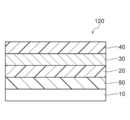
- FIG. 4 is a schematic diagram showing an example of the layer structure of the laminate according to the present disclosure.
- FIG. 5 is a schematic diagram showing an example of the layer configuration of the laminate according to the present disclosure.
- FIG. 6 is a schematic diagram showing the pattern A.
- the numerical range represented by “to” means a range including the numerical values before and after “to” as the lower limit value and the upper limit value.
- the upper limit value or the lower limit value described in a certain numerical range may be replaced with the upper limit value or the lower limit value of another stepwise described numerical range.
- the upper limit value or the lower limit value described in a certain numerical range may be replaced with the values shown in the examples.
- “(meth)acrylic” means both acrylic and methacrylic, or either
- “(meth)acrylate” means both acrylate and methacrylate or either one.
- (meth)acryloxy means both acryloxy and methacryloxy, or either one.
- the amount of each component in the composition means the total amount of the plurality of substances present in the composition, unless there is a plurality of substances corresponding to each component in the composition, unless otherwise specified. ..
- the term “step” is included in the term as long as the intended purpose of the step is achieved not only as an independent step but also when it cannot be clearly distinguished from other steps. .. In the notation of a group (atomic group) in the present disclosure, notation that does not indicate substituted or unsubstituted encompasses not only those having no substituent but also those having a substituent.
- an “alkyl group” includes not only an alkyl group having no substituent (unsubstituted alkyl group) but also an alkyl group having a substituent (substituted alkyl group).
- “mass %” and “weight %” have the same meaning
- “mass part” and “weight part” have the same meaning.
- a combination of two or more preferable aspects is a more preferable aspect.
- the chemical structural formula may be described as a simplified structural formula in which a hydrogen atom is omitted.
- the ratio of the structural units in the resin represents a molar ratio unless otherwise specified.
- the molecular weight in the case where there is a molecular weight distribution represents the weight average molecular weight (Mw) unless otherwise specified.
- the conductive transfer material according to the present disclosure includes a temporary support, a first resin layer having a thickness of 1 nm to 300 nm, and a layer containing silver nanowires (hereinafter, also referred to as “silver nanowire layer”). , In that order.
- the conductive transfer material according to the present disclosure has a temporary support, a first resin layer having a thickness of 1 nm to 300 nm, and a layer containing silver nanowires in this order, thereby forming a pattern.
- the step difference caused by the pattern can be reduced, it is possible to suppress the occurrence of a planar abnormality at the adhesion interface between the pattern and the layer laminated on the pattern.
- FIG. 1 schematically shows an example of the layer structure of the conductive transfer material according to the present disclosure.
- the conductive transfer material 100 shown in FIG. 1 has a temporary support 10, a first resin layer 20, and a layer 30 containing silver nanowires in this order. It should be noted that the scale of each element shown in the drawings of the present disclosure is not necessarily accurate.
- the conductive transfer material according to the present disclosure has a temporary support.
- the temporary support is a support that supports at least the first resin layer and the layer containing the silver nanowires and can be peeled from the adherend (for example, the first resin layer).
- the temporary support preferably has optical transparency from the viewpoint that pattern exposure can be performed via the temporary support.
- “having optical transparency” means that the transmittance of the dominant wavelength of light used for pattern exposure is 50% or more. From the viewpoint of improving the exposure sensitivity, the transmittance of the main wavelength of light used for pattern exposure is preferably 60% or more, more preferably 70% or more. Examples of the method for measuring the transmittance include a method using a spectrophotometer (for example, MCPD-6800 manufactured by Otsuka Electronics Co., Ltd.).
- the temporary support examples include a glass base material, a resin film, paper and the like.
- the temporary support is preferably a resin film from the viewpoint of strength and flexibility.
- the temporary support it is possible to use a resin film which is flexible and does not significantly deform, shrink, or stretch under pressure or under pressure and heating.
- the resin film used as the temporary support is free from deformation such as wrinkles and scratches.
- the resin film include cycloolefin polymer film, polyethylene terephthalate film (for example, biaxially stretched polyethylene terephthalate film), cellulose triacetate film, polystyrene film, polyimide film, polycarbonate film and the like.
- the temporary support is preferably polyethylene terephthalate, and more preferably a biaxially stretched polyethylene terephthalate film, from the viewpoint of optical properties.
- Examples of the temporary support include a biaxially stretched polyethylene terephthalate film having a thickness of 16 ⁇ m, a biaxially stretched polyethylene terephthalate film having a thickness of 12 ⁇ m, and a biaxially stretched polyethylene terephthalate film having a thickness of 9 ⁇ m. ..
- the transparency of the temporary support is preferably high from the viewpoint that pattern exposure can be performed through the temporary support.
- the transmittance of the temporary support at a wavelength of 365 nm is preferably 60% or more, more preferably 70% or more.
- the haze of the temporary support is preferably small.
- the haze value of the temporary support is preferably 2% or less, more preferably 0.5% or less, and particularly preferably 0.1% or less.
- the number of fine particles, foreign matters, and defects contained in the temporary support be small.
- the number of fine particles having a diameter of 1 ⁇ m or more, foreign matters, and defects is preferably 50 pieces/10 mm 2 or less, more preferably 10 pieces/10 mm 2 or less, and further preferably 3 pieces/10 mm 2 or less. It is particularly preferable that the number is 0/10 mm 2 .
- a layer (lubricant layer) containing fine particles may be provided on the surface of the temporary support from the viewpoint of imparting handleability.
- the lubricant layer may be provided on one side or both sides of the temporary support.
- the diameter of the particles contained in the lubricant layer can be 0.05 ⁇ m to 0.8 ⁇ m.
- the thickness of the lubricant layer can be 0.05 ⁇ m to 1.0 ⁇ m.
- the thickness of the temporary support is not limited and can be set appropriately according to the material.
- the thickness of the temporary support is preferably 5 ⁇ m to 200 ⁇ m, more preferably 10 ⁇ m to 150 ⁇ m, and particularly preferably 10 ⁇ m to 50 ⁇ m, from the viewpoint of ease of handling and versatility.
- the conductive transfer material according to the present disclosure has a layer containing silver nanowires.
- the diameter (that is, the minor axis length) of the silver nanowires is preferably 50 nm or less, more preferably 35 nm or less, and particularly preferably 20 nm or less.
- the diameter of the silver nanowire is preferably 5 nm or more from the viewpoint of oxidation resistance and durability.
- the length of the silver nanowire (that is, the major axis length) is preferably 5 ⁇ m or more, more preferably 10 ⁇ m or more, and particularly preferably 30 ⁇ m or more.
- the length (long axis length) of the silver nanowires is preferably 1 mm or less from the viewpoint that aggregates are generated in the manufacturing process.
- the diameter and length of the silver nanowire can be measured using, for example, a transmission electron microscope (TEM) or an optical microscope. Specifically, the diameter and length of each silver nanowire measured by observing 300 silver nanowires using a transmission electron microscope or an optical microscope are arithmetically averaged, and the obtained value is the silver nanowire.
- TEM transmission electron microscope
- optical microscope optical microscope
- the shape of the silver nanowire examples include a columnar shape, a rectangular parallelepiped shape, and a columnar shape having a polygonal cross section.
- the shape of the silver nanowire is preferably at least one of a columnar shape and a cross-sectional shape with rounded corners.
- the cross-sectional shape of the silver nanowire can be observed using a transmission electron microscope (TEM).
- the content of the silver nanowires in the layer containing the silver nanowires is preferably 1% by mass to 99% by mass with respect to the total mass of the layer containing the silver nanowires from the viewpoint of transparency and conductivity. More preferably, it is 10% by mass to 95% by mass.
- the layer containing silver nanowires may contain a binder (also referred to as a matrix), if necessary.
- the binder is a solid material in which silver nanowires are dispersed or embedded.
- the binder can protect the silver nanowires from harmful environmental factors such as corrosion and abrasion.
- binder for example, a polymer material, an inorganic material and the like can be mentioned, and a material having light transmittance is preferable.
- the polymer material examples include (meth)acrylic resin (for example, poly(methyl methacrylate)), polyester (for example, polyethylene terephthalate (PET)), polycarbonate, polyimide, polyamide, polyolefin (for example, polypropylene), polynorbornene. , Cellulose compounds, polyvinyl alcohol (PVA), polyvinyl pyrrolidone, and the like.
- the cellulose compound include hydroxypropylmethyl cellulose (HPMC), hydroxyethyl cellulose (HEC), methyl cellulose (MC), hydroxypropyl cellulose (HPC), carboxymethyl cellulose (CMC) and the like.
- the polymer material may be a conductive polymer material. Examples of the conductive polymer material include polyaniline and polythiophene.
- Examples of the inorganic material include silica, mullite, alumina and the like.
- the materials described in paragraphs 0051 to 0052 of JP2014-212117A can be used. These descriptions are incorporated herein by reference.
- the layer containing silver nanowires may contain one kind of binder or two or more kinds of binders.
- the content of the binder in the layer containing silver nanowires may be 1% by mass to 99% by mass with respect to the total mass of the layer containing silver nanowires. It is more preferably 5% by mass to 80% by mass.
- the thickness of the layer containing silver nanowires is preferably 1 nm to 400 nm, more preferably 10 nm to 200 nm, from the viewpoint of transparency and conductivity.
- the thickness of the layer containing silver nanowires is measured by the following method.
- the arithmetic mean value of the thicknesses of the layer containing silver nanowires measured at 10 randomly selected points was calculated, and the obtained value was calculated as the silver nanowire.
- the cross-sectional observation image in the thickness direction of the layer containing silver nanowires can be obtained using a scanning electron microscope (SEM) or a transmission electron microscope (TEM).
- the minimum transmittance of the layer containing silver nanowires at a wavelength of 400 nm to 700 nm is preferably 80% or more, and more preferably 90% or more.
- the transmittance is measured by the same method as the method for measuring the transmittance of the temporary support.
- the method for producing the silver nanowire is not limited, and a known method can be applied.
- a method for producing the silver nanowires for example, a step of adding a silver complex solution to an aqueous solvent containing at least a halogen compound and a reducing agent and heating at a temperature of 150° C. or lower, and desalting as necessary. Examples include a method having a treatment step.
- the halogen compound is not limited as long as it is a compound containing bromine, chlorine, or iodine.
- the halogen compound include alkali halides such as sodium bromide, sodium chloride, sodium iodide, potassium iodide, potassium bromide and potassium chloride.
- HTAB hexadecyltrimethylammonium bromide
- HTAC hexadecyltrimethylammonium chloride
- Examples of the reducing agent include borohydride metal salts such as sodium borohydride and potassium borohydride; lithium aluminum hydride, potassium aluminum hydride, cesium aluminum hydride, beryllium aluminum hydride, magnesium aluminum hydride, hydrogen Aluminum hydride salts such as calcium aluminum hydride; sodium sulfite, hydrazine compound, dextrin, hydroquinone, hydroxylamine, citric acid or its salt, succinic acid or its salt, ascorbic acid or its salt, etc.; diethylaminoethanol, ethanolamine, propanolamine , Alkanolamines such as triethanolamine and dimethylaminopropanol; aliphatic amines such as propylamine, butylamine, dipropyleneamine, ethylenediamine and triethylenepentamine; heterocyclic amines such as piperidine, pyrrolidine, N-methylpyrrolidine and morpholine Aromatic amines such as aniline, N-methylaniline,
- Examples of the ligand of the silver complex include CN ⁇ , SCN ⁇ , SO 3 2 ⁇ , thiourea, ammonia and the like.
- a silver ammonia complex is preferable.
- the heating temperature is preferably 150° C. or lower, more preferably 20° C. to 130° C., further preferably 30° C. to 100° C., and particularly preferably 40° C. to 90° C.
- the desalting treatment can be performed by a method such as ultrafiltration, dialysis, gel filtration, decantation, and centrifugation after forming the silver nanowires.
- the method for forming the layer containing silver nanowires is not limited, and a known method can be applied.
- Examples of the method of forming the layer containing silver nanowires include a method of applying a coating liquid for forming a silver nanowire layer containing the above-mentioned components onto an object to be coated, and drying the coating solution.
- the coating liquid for forming the silver nanowire layer can be prepared, for example, by mixing the above components and a solvent in an arbitrary ratio.
- Water is mainly used as the solvent, and an organic solvent miscible with water can be used together in a proportion of 80% by volume or less with respect to the total amount of the solvent.
- an alcohol compound having a boiling point of 50° C. to 250° C., more preferably 55° C. to 200° C. is preferable.
- the alcohol compound include methanol, ethanol, ethylene glycol, diethylene glycol, triethylene glycol, polyethylene glycol 200, polyethylene glycol 300, glycerin, propylene glycol, dipropylene glycol, 1,3-propanediol, 1,2-butanediol.
- Examples thereof include 1,4-butanediol, 1,5-pentanediol, 1-ethoxy-2-propanol, ethanolamine, diethanolamine, 2-(2-aminoethoxy)ethanol, 2-dimethylaminoisopropanol and the like.
- the content of the silver nanowires in the coating liquid for forming the silver nanowire layer is preferably 0.01% by mass to 99% by mass with respect to the total mass of the coating liquid for forming the silver nanowire layer, It is more preferably from 05% by mass to 95% by mass.
- coating methods include slit coating, spin coating, curtain coating, inkjet coating, and the like.
- the drying temperature can be set appropriately according to the type of volatile components such as solvent.
- the drying temperature can be set, for example, in the range of 60°C to 120°C.
- the conductive transfer material according to the present disclosure has a first resin layer having a thickness of 1 nm to 300 nm. Since the conductive transfer material has the first resin layer having a thickness of 1 nm to 300 nm, the step caused by the pattern can be reduced, and thus the surface abnormality at the adhesion interface between the pattern and the layer laminated on the pattern can be reduced. Can be suppressed.
- the thickness of the first resin layer is 1 nm to 300 nm, preferably 1 nm to 200 nm, more preferably 1 nm to 150 nm, and further preferably 1 nm to 100 nm, from the viewpoint of suppressing the occurrence of planar abnormalities. Is particularly preferable.
- the thickness of the first resin layer may be 1 nm to 70 nm, or 1 nm to 30 nm.
- the thickness of the first resin layer can be measured by the method described in the above section "Layer containing silver nanowires".
- the minimum transmittance of the first resin layer at a wavelength of 400 nm to 700 nm is preferably 80% or more, and more preferably 90% or more.
- the transmittance is measured by the same method as the method for measuring the transmittance of the temporary support.
- the first resin layer is preferably a photosensitive resin layer from the viewpoint of patterning property.
- the photosensitive resin layer include a positive photosensitive resin layer and a negative photosensitive resin layer.
- the first resin layer is preferably a negative photosensitive resin layer from the viewpoint of chemical resistance and durability.
- the positive photosensitive resin layer is not limited, and a known positive photosensitive resin layer can be applied. From the viewpoint of sensitivity, resolution, and removability, the positive photosensitive resin layer contains a polymer containing a structural unit having an acid group protected by an acid-decomposable group, and a photo-acid generator. Is preferred.
- the positive type photosensitive resin layer is described in paragraphs 0033 to 0130 of International Publication No. 2018/179640. These descriptions are incorporated herein by reference.
- the positive photosensitive resin layer contains a polymer (hereinafter, also referred to as “polymer A”) containing a structural unit (hereinafter, also referred to as “structural unit A”) having an acid group that is acid-decomposable and protected. It is preferable to contain The acid group protected by the acid-decomposable group in the polymer A becomes an acid group by the action of a catalytic amount of acid generated by exposure (that is, deprotection reaction). The acid group generated by the deprotection reaction enables the positive photosensitive resin layer to be dissolved in the developing solution.
- the polymer A is preferably an addition polymerization type polymer, and more preferably a polymer containing a structural unit derived from (meth)acrylic acid or its ester.
- a structural unit other than the structural unit derived from (meth)acrylic acid or its ester for example, the structural unit derived from a styrene compound, the structural unit derived from a vinyl compound, etc.
- the acid group in the structural unit A is not limited, and known acid groups can be applied.
- the acid group is preferably a carboxy group or a phenolic hydroxyl group (also referred to as "phenolic hydroxy group").
- the acid-decomposable group in the structural unit A is not limited, and known acid-decomposable groups can be applied.
- the acid-decomposable group include groups that are relatively easily decomposed by acid (eg, acetal-type functional groups such as 1-alkoxyalkyl group, tetrahydropyranyl group, and tetrahydrofuranyl group), groups that are relatively difficult to be decomposed by acid. (For example, a tertiary alkyl group such as a tert-butyl group).
- the acid-decomposable group is preferably a group having a structure that protects the acid group in the form of acetal.
- the acid-decomposable group is preferably an acid-decomposable group having a molecular weight of 300 or less from the viewpoint of suppressing variation in the line width of the conductive wiring when applied to the formation of a conductive pattern.
- the structural unit having an acid group protected by an acid-decomposable group is a structural unit represented by the following formula A1 and a structural unit represented by the following formula A2 from the viewpoints of suppressing deformation of the pattern shape, solubility in a developing solution, and transferability.
- At least one structural unit selected from the group consisting of structural units represented by the following formula A3 and structural units represented by the following formula A3 is preferable, and structural units represented by the following formula A3 are preferable, A structural unit represented by formula A3-3 described later is particularly preferable.
- the structural unit represented by the following formula A1 and the structural unit represented by the following formula A2 are structural units having a phenolic hydroxyl group protected by an acid-decomposable group.
- the structural unit represented by the following formula A3 is a structural unit having a carboxy group protected by an acid-decomposable group.
- R 11 and R 12 each independently represent a hydrogen atom, an alkyl group, or an aryl group, at least one of R 11 and R 12 is an alkyl group, or an aryl group, and R 13 is , R 11 or R 12 and R 13 may be linked to each other to form a cyclic ether, R 14 represents a hydrogen atom or a methyl group, and X 1 represents It represents a single bond or a divalent linking group, R 15 represents a substituent, and n represents an integer of 0 to 4.
- R 21 and R 22 each independently represent a hydrogen atom, an alkyl group, or an aryl group, at least one of R 21 and R 22 is an alkyl group or an aryl group, and R 23 is an alkyl group.
- R 21 or R 22 and R 23 may be linked to each other to form a cyclic ether, and R 24 is independently a hydroxy group, a halogen atom, an alkyl group or an alkoxy group.
- R 31 and R 32 each independently represent a hydrogen atom, an alkyl group, or an aryl group, at least one of R 31 and R 32 is an alkyl group or an aryl group, and R 33 is It represents an alkyl group or an aryl group, and R 31 or R 32 and R 33 may be linked to each other to form a cyclic ether, R 34 represents a hydrogen atom or a methyl group, and X 0 represents a single atom. It represents a bond or a linking group, and Y represents a sulfur atom or an oxygen atom.
- R 31 or R 32 when R 31 or R 32 is an alkyl group, the alkyl group is preferably an alkyl group having 1 to 10 carbon atoms.
- the aryl group is preferably a phenyl group.
- R 31 and R 32 are each independently a hydrogen atom or an alkyl group having 1 to 4 carbon atoms, and at least one of R 31 and R 32 is preferably an alkyl group having 1 to 4 carbon atoms.
- R 33 is preferably an alkyl group having 1 to 10 carbon atoms, and more preferably an alkyl group having 1 to 6 carbon atoms.
- the alkyl group and aryl group for R 31 to R 33 may have a substituent.
- R 31 or R 32 and R 33 are preferably linked to each other to form a cyclic ether.
- the number of ring members of the cyclic ether is not limited, but is preferably 5 or 6, and more preferably 5.
- X 0 is preferably a single bond or an arylene group, and more preferably a single bond.
- the arylene group may have a substituent.
- Y is preferably an oxygen atom from the viewpoint of exposure sensitivity.
- R 34 represents a hydrogen atom or a methyl group, and is preferably a hydrogen atom from the viewpoint that the glass transition temperature (Tg) of the polymer A can be further lowered. More specifically, the content ratio of the structural unit in which R 34 in the formula A3 is a hydrogen atom is 20 mol% or more based on all the structural units represented by the formula A3 contained in the polymer A. preferable.
- the content ratio (mol %) of the structural unit in which R 34 in the formula A3 is a hydrogen atom in the structural unit represented by the formula A3 is calculated by a conventional method from 13 C-nuclear magnetic resonance spectrum (NMR) measurement. Confirm by the intensity ratio of the peak intensity.
- constitutional unit represented by the formula A3 is more preferable from the viewpoint of further increasing the sensitivity during pattern formation.
- R 34 represents a hydrogen atom or a methyl group
- R 35 to R 41 each independently represent a hydrogen atom or an alkyl group having 1 to 4 carbon atoms.
- R 34 is preferably a hydrogen atom.
- R 35 to R 41 are preferably hydrogen atoms.
- R ⁇ 34 > in the following structural units represents a hydrogen atom or a methyl group.
- the polymer A may have one type of structural unit A, or may have two or more types of structural unit A.
- the content ratio of the structural unit A in the polymer A is preferably 10 mol% or more, more preferably 10 mol% to 90 mol%, and more preferably 20 mol% with respect to all the structural units of the polymer A. It is particularly preferable that the content is ⁇ 70 mol %.
- the content ratio of the structural unit A in the polymer A is confirmed by the intensity ratio of peak intensities calculated by a conventional method from 13 C-NMR measurement.
- the polymer A preferably contains a structural unit having an acid group (hereinafter, also referred to as “structural unit B”).
- structural unit B a structural unit having an acid group
- the acid group in the structural unit B means a proton dissociative group having a pKa of 12 or less.
- the pKa of the acid group is preferably 10 or less, and more preferably 6 or less.
- the pKa of the acid group is preferably ⁇ 5 or more.
- Examples of the acid group in the structural unit B include a carboxy group, a sulfonamide group, a phosphonic acid group, a sulfonic acid group, a phenolic hydroxyl group, a sulfonylimide group, and the like.
- the acid group is preferably a carboxy group or a phenolic hydroxyl group.
- the introduction of the structural unit having an acid group into the polymer A can be carried out by copolymerizing a monomer having an acid group.
- the constituent unit B is more preferably a constituent unit in which a constituent unit derived from a styrene compound or a constituent unit derived from a vinyl compound is substituted with an acid group, or a constituent unit derived from (meth)acrylic acid.
- the structural unit B is preferably at least one structural unit selected from the group consisting of a structural unit having a carboxy group and a structural unit having a phenolic hydroxyl group, from the viewpoint of better sensitivity during pattern formation. ..
- the polymer A may contain one type of structural unit B and may contain two or more types of structural unit B.
- the content ratio of the structural unit B in the polymer A is preferably 0.1 mol% to 20 mol %, and 0.5 mol% with respect to all the structural units of the polymer A. It is more preferably from 15 to 15 mol %, particularly preferably from 1 to 10 mol %.
- the content ratio of the structural unit B in the polymer A is confirmed by the intensity ratio of the peak intensities calculated by the usual method from 13 C-NMR measurement.
- the polymer A is a constitutional unit other than the constitutional unit A and the constitutional unit B described above (hereinafter, also referred to as “constitutional unit C”) as long as the effect of the conductive transfer material according to the present disclosure is not impaired. May be included.
- Examples of the monomer forming the structural unit C include styrene compounds, (meth)acrylic acid alkyl esters, (meth)acrylic acid cyclic alkyl esters, (meth)acrylic acid aryl esters, unsaturated dicarboxylic acid diesters, and bicyclo unsaturated compounds.
- Maleimide compounds, unsaturated aromatic compounds, conjugated diene compounds, unsaturated monocarboxylic acids, unsaturated dicarboxylic acids, unsaturated dicarboxylic acid anhydrides, unsaturated compounds having an aliphatic cyclic skeleton, other unsaturated compounds, etc. Are listed.
- structural unit C specifically, styrene, tert-butoxystyrene, methylstyrene, ⁇ -methylstyrene, acetoxystyrene, methoxystyrene, ethoxystyrene, chlorostyrene, methyl vinylbenzoate, ethyl vinylbenzoate, (meta ) Methyl acrylate, ethyl (meth)acrylate, n-propyl (meth)acrylate, isopropyl (meth)acrylate, 2-hydroxyethyl (meth)acrylate, 2-hydroxypropyl (meth)acrylate, (meth ) Structural units formed by polymerizing benzyl acrylate, isobornyl (meth)acrylate, acrylonitrile, ethylene glycol monoacetoacetate mono(meth)acrylate and the like.
- Other examples include structural units formed by polymerizing the compounds described in paragraphs 0021 to 00
- the structural unit C at least one structural unit selected from the group consisting of a structural unit having an aromatic ring and a structural unit having an aliphatic cyclic skeleton from the viewpoint of improving the electrical characteristics of the resulting conductive transfer material.
- the monomer forming the above structural unit include styrene, tert-butoxystyrene, methylstyrene, ⁇ -methylstyrene, dicyclopentanyl (meth)acrylate, cyclohexyl (meth)acrylate, isobornyl (meth)acrylate, benzyl (meth). ) Acrylate and the like.
- the structural unit C is preferably a structural unit derived from cyclohexyl (meth)acrylate.
- the monomer forming the structural unit C is preferably (meth)acrylic acid alkyl ester, and more preferably (meth)acrylic acid alkyl ester having an alkyl group having 4 to 12 carbon atoms. .. Specific examples include methyl (meth)acrylate, ethyl (meth)acrylate, propyl (meth)acrylate, n-butyl (meth)acrylate, and 2-ethylhexyl (meth)acrylate.
- Polymer A may contain one type of structural unit C, or may contain two or more types of structural unit C.
- the content ratio of the structural unit C in the polymer A is preferably 70 mol% or less, more preferably 60 mass% or less, particularly preferably 50 mass% or less, based on all the structural units of the polymer A.
- the lower limit of the content ratio of the structural unit C in the polymer A may be 0 mol %.
- the content ratio of the structural unit C in the polymer A is preferably 1 mol% or more, more preferably 5 mol% or more, based on all the structural units of the polymer A. Within the above range, the resolution and the adhesiveness are further improved.
- the weight average molecular weight of the polymer A is preferably 60,000 or less.
- the weight average molecular weight of the polymer A is 60,000 or less, it is possible to suppress the melt viscosity of the photosensitive resin layer to a low level and to realize the bonding at a low temperature (for example, 130° C. or less) when bonding the substrate. it can.
- the weight average molecular weight of the polymer A is preferably 2,000 to 60,000, and more preferably 3,000 to 50,000.
- the weight average molecular weight of the polymer A is a polystyrene equivalent weight average molecular weight measured by the method described above (that is, gel permeation chromatography).
- the positive photosensitive resin layer may contain one type of polymer A or may contain two or more types of polymer A.
- the content of the polymer A in the positive photosensitive resin layer is from 50% by mass to 99.% with respect to the total mass of the positive photosensitive resin layer from the viewpoint of exhibiting good adhesion to the substrate. It is preferably 9% by mass, and more preferably 70% by mass to 98% by mass.
- the production method (synthesis method) of the polymer A is not limited, and known methods can be applied.
- a method for producing the polymer A for example, a polymerizable monomer for forming the structural unit A, a polymerizable monomer for forming a structural unit B having an acid group, and a structural unit C are further added, if necessary.
- the method of polymerizing the polymerizable monomer for forming in an organic solvent using a polymerization initiator is mentioned.
- the positive photosensitive resin layer preferably contains a photoacid generator.
- a photoacid generator is a compound that can generate an acid by being irradiated with radiation such as ultraviolet rays, far ultraviolet rays, X-rays, and charged particle beams.
- the photoacid generator is preferably a compound which reacts with an actinic ray having a wavelength of 300 nm or more, preferably 300 nm to 450 nm to generate an acid.
- a photo-acid generator which is not directly sensitive to an actinic ray having a wavelength of 300 nm or more, when used in combination with a sensitizer, it is a compound which is sensitive to an actinic ray having a wavelength of 300 nm or more and generates an acid. It can be preferably used in combination.
- the photoacid generator is preferably a photoacid generator that generates an acid with a pKa of 4 or less, more preferably a photoacid generator that generates an acid with a pKa of 3 or less, and a light that generates an acid with a pKa of 2 or less. Acid generators are particularly preferred.
- the lower limit of pKa is not specified.
- the pKa is preferably, for example, -10.0 or more.
- the photoacid generator includes, for example, an ionic photoacid generator and a nonionic photoacid generator. From the viewpoint of sensitivity and resolution, the photoacid generator preferably contains at least one compound selected from the group consisting of an onium salt compound described below and an oxime sulfonate compound described below, and contains an oxime sulfonate compound. More preferable.
- the ionic photoacid generator examples include onium salt compounds such as diaryliodonium salt compounds and triarylsulfonium salt compounds, and quaternary ammonium salt compounds.
- the ionic photoacid generator is preferably an onium salt compound, and more preferably at least one of a triarylsulfonium salt compound and a diaryliodonium salt compound.
- the ionic photoacid generator described in paragraphs 0114 to 0133 of JP-A-2014-85643 can also be preferably used.
- nonionic photoacid generator examples include a trichloromethyl-s-triazine compound, a diazomethane compound, an imide sulfonate compound, an oxime sulfonate compound and the like.
- the nonionic photoacid generator is preferably an oxime sulfonate compound from the viewpoint of sensitivity, resolution, and adhesiveness.
- Specific examples of the trichloromethyl-s-triazine compound and the diazomethane compound include the compounds described in paragraphs 0083 to 0088 of JP 2011-221494A.
- oxime sulfonate compound that is, the compound having an oxime sulfonate structure
- a compound having an oxime sulfonate structure represented by the following formula (B1) is preferable.
- R 21 represents an alkyl group or an aryl group
- * represents a bonding site with another atom or another group.
- any group may be substituted, and the alkyl group for R 21 may be linear or branched, It may have a ring structure.
- the permissible substituents are described below.
- the alkyl group represented by R 21 is preferably a linear or branched alkyl group having 1 to 10 carbon atoms.
- the alkyl group represented by R 21 may be substituted with an aryl group having 6 to 11 carbon atoms, an alkoxy group having 1 to 10 carbon atoms, a cycloalkyl group, or a halogen atom.
- the aryl group represented by R 21 is preferably an aryl group having 6 to 18 carbon atoms, and more preferably a phenyl group or a naphthyl group.
- the aryl group represented by R 21 may be substituted with one or more groups selected from the group consisting of an alkyl group having 1 to 4 carbon atoms, an alkoxy group and a halogen atom.
- the positive photosensitive resin layer may contain one type of photo-acid generator, or may contain two or more types of photo-acid generator.
- the content of the photo-acid generator in the positive photosensitive resin layer is 0.1% by mass to 10% by mass based on the total mass of the positive photosensitive resin layer. Is preferred, and more preferably 0.5% by mass to 5% by mass.
- the positive photosensitive resin layer may contain a component other than the above components (hereinafter, also referred to as “other component A”).
- the other component A is not limited and can be appropriately selected depending on the purpose and the like.
- Other components include, for example, a surfactant and a corrosion inhibitor described later.
- surfactants include anionic surfactants, cationic surfactants, nonionic (nonionic) surfactants, and amphoteric surfactants.
- the positive photosensitive resin layer contains a surfactant, the uniformity of the film thickness can be improved.
- the surfactant is preferably a nonionic surfactant.
- nonionic surfactants examples include polyoxyethylene higher alkyl ether surfactants, polyoxyethylene higher alkyl phenyl ether surfactants, higher fatty acid diester surfactants of polyoxyethylene glycol, and silicone surfactants. Agents, fluorine-based surfactants and the like. Specific examples of the nonionic surfactant include KP (manufactured by Shin-Etsu Chemical Co., Ltd.), Polyflow (manufactured by Kyoeisha Chemical Co., Ltd.), F-top (manufactured by JEMCO), Megafac (registered trademark, for example, Megafac F551A, DIC).
- the positive photosensitive resin layer may contain one kind of surfactant or may contain two or more kinds of surfactant.
- the content of the surfactant in the positive photosensitive resin layer is 0.05% by mass to 10% by mass with respect to the total mass of the positive photosensitive resin layer from the viewpoint of uniformity of film thickness. It is preferable that the content is 0.05% by mass to 5% by mass.
- the negative photosensitive resin layer is not limited, and a known negative photosensitive resin layer can be applied.
- the negative photosensitive resin layer preferably contains a polymerizable compound, a polymerization initiator, and a binder polymer from the viewpoint of pattern formability.
- the negative photosensitive resin layer preferably contains a polymerizable compound.
- the polymerizable compound includes a polymerizable compound such as a radical polymerizable compound and a cationic polymerizable compound.
- the polymerizable compound is preferably a photopolymerizable compound, and more preferably an ethylenically unsaturated compound.
- An ethylenically unsaturated compound is a compound that has one or more ethylenically unsaturated groups.
- a (meth)acryloyl group is more preferable.
- a (meth)acrylate compound is preferable.
- the ethylenically unsaturated compound preferably contains a bifunctional or higher functional ethylenically unsaturated compound.
- the bifunctional or higher functional ethylenically unsaturated compound means a compound having two or more ethylenically unsaturated groups in one molecule.
- bifunctional ethylenically unsaturated compound examples include tricyclodecane dimethanol di(meth)acrylate, 1,9-nonanediol di(meth)acrylate, and 1,6-hexanediol di(meth)acrylate.
- bifunctional ethylenically unsaturated compound examples include tricyclodecane dimethanol diacrylate (A-DCP, manufactured by Shin-Nakamura Chemical Co., Ltd.), tricyclodecane dimethanol dimethacrylate (DCP, new Nakamura Chemical Co., Ltd.), 1,9-Nonanediol diacrylate (A-NOD-N, Shin-Nakamura Chemical Co., Ltd.), 1,6-hexanediol diacrylate (A-HD-N, New) Nakamura Chemical Co., Ltd.), polytetramethylene glycol #650 diacrylate (A-PTMG-65, Shin Nakamura Chemical Co., Ltd.) and the like.
- A-DCP tricyclodecane dimethanol diacrylate
- DCP new Nakamura Chemical Co., Ltd.
- 1,9-Nonanediol diacrylate A-NOD-N, Shin-Nakamura Chemical Co., Ltd.
- Examples of the trifunctional or higher functional ethylenically unsaturated compound include dipentaerythritol (tri/tetra/penta/hexa)(meth)acrylate, pentaerythritol (tri/tetra)(meth)acrylate, trimethylolpropane tri(meth)acrylate.
- Examples thereof include acrylate, ditrimethylolpropane tetra(meth)acrylate, isocyanuric acid (meth)acrylate, and (meth)acrylate compound having a glycerin tri(meth)acrylate skeleton.
- (tri/tetra/penta/hexa)(meth)acrylate includes tri(meth)acrylate, tetra(meth)acrylate, penta(meth)acrylate, and hexa(meth)acrylate. It is a concept. Further, the term “(tri/tetra)(meth)acrylate” is a concept including tri(meth)acrylate and tetra(meth)acrylate.
- the ethylenically unsaturated compound preferably contains an ethylenically unsaturated compound having an acid group.
- the acid group include a phosphoric acid group, a sulfonic acid group, a carboxy group and the like, and a carboxy group is preferable.
- Examples of the ethylenically unsaturated compound having an acid group include a 3- to 4-functional ethylenically unsaturated compound having an acid group and a 5- to 6-functional ethylenically unsaturated compound having an acid group.
- Examples of the bifunctional or higher functional ethylenically unsaturated compound having a carboxy group include Aronix (registered trademark) TO-2349 (manufactured by Toagosei Co., Ltd.), Aronix M-520 (manufactured by Toagosei Co., Ltd.), and Aronix M-. 510 (manufactured by Toagosei Co., Ltd.) is preferable.
- the ethylenically unsaturated compound having an acid group is also preferably a polymerizable compound having an acid group described in paragraphs 0025 to 0030 of JP 2004-239942A.
- the contents of the above documents are incorporated herein.
- the negative photosensitive resin layer may contain one type of polymerizable compound or may contain two or more types of polymerizable compounds.
- the content of the polymerizable compound in the negative photosensitive resin layer is preferably 1% by mass to 70% by mass with respect to the total mass of the negative photosensitive resin layer.
- the content is more preferably from mass% to 70 mass%, further preferably from 5 mass% to 60 mass%, particularly preferably from 8 mass% to 50 mass%.
- the negative photosensitive resin layer preferably contains a polymerization initiator.
- the polymerization initiator at least one of a photopolymerization initiator and a thermal polymerization initiator is preferable, and a photopolymerization initiator is more preferable.
- the photopolymerization initiator examples include a photopolymerization initiator having an oxime ester structure (hereinafter, also referred to as “oxime-based photopolymerization initiator”) and a photopolymerization initiator having an ⁇ -aminoalkylphenone structure (hereinafter, “ Also referred to as " ⁇ -aminoalkylphenone-based photopolymerization initiator”), a photopolymerization initiator having an ⁇ -hydroxyalkylphenone structure (hereinafter also referred to as " ⁇ -hydroxyalkylphenone-based polymerization initiator”), acylphosphine.
- oxime-based photopolymerization initiator also referred to as “oxime-based photopolymerization initiator”
- ⁇ -aminoalkylphenone-based photopolymerization initiator a photopolymerization initiator having an ⁇ -aminoalkylphenone structure
- a photopolymerization initiator having an oxide structure hereinafter, also referred to as “acylphosphine oxide-based photopolymerization initiator”
- acylphosphine oxide-based photopolymerization initiator a photopolymerization initiator having an N-phenylglycine structure
- N-phenylglycine-based photopolymerization initiator a photopolymerization initiator having an N-phenylglycine structure
- agent also referred to as “agent”
- the photopolymerization initiator is selected from the group consisting of oxime photopolymerization initiators, ⁇ -aminoalkylphenone photopolymerization initiators, ⁇ -hydroxyalkylphenone photopolymerization initiators, and N-phenylglycine photopolymerization initiators. At least one selected from the group consisting of oxime-based photopolymerization initiators, ⁇ -aminoalkylphenone-based photopolymerization initiators, and N-phenylglycine-based photopolymerization initiators. Is more preferable.
- the photopolymerization initiator for example, the photopolymerization initiators described in paragraphs 0031 to 0042 of JP2011-95716A and paragraphs 0064 to 0081 of JP2015-014783A may be used.
- photopolymerization initiators examples include 1-[4-(phenylthio)phenyl]-1,2-octanedione-2-(O-benzoyloxime) (trade name: IRGACURE (registered trademark) OXE-01 , Manufactured by BASF), 1-[9-ethyl-6-(2-methylbenzoyl)-9H-carbazol-3-yl]ethanone-1-(O-acetyloxime) (trade name: IRGACURE OXE-02, BASF 2-(dimethylamino)-2-[(4-methylphenyl)methyl]-1-[4-(4-morpholinyl)phenyl]-1-butanone (trade name: IRGACURE 379EG, BASF) , 2-methyl-1-(4-methylthiophenyl)-2-morpholinopropan-1-one (trade name: IRGACURE 907, manufactured by BASF), 2-hydroxy-1- ⁇ 4-[4-(2- Hydroxy-2-
- the negative photosensitive resin layer may contain one type of polymerization initiator or may contain two or more types of polymerization initiators.
- the content of the polymerization initiator in the negative photosensitive resin layer is preferably 0.1% by mass or more, more preferably 0.2% by mass or more, based on the total mass of the negative photosensitive resin layer. It is particularly preferably 0.3% by mass or more.
- the content of the polymerization initiator in the negative photosensitive resin layer is preferably 10% by mass or less, more preferably 5% by mass or less, based on the total mass of the negative photosensitive resin layer.
- the negative photosensitive resin layer preferably contains a binder polymer.
- the binder polymer is preferably an alkali-soluble resin from the viewpoint of developability.
- the alkali-soluble resin is preferably a resin having an acid value of 60 mgKOH/g or more, and is a (meth)acrylic resin having a carboxy group (hereinafter, also referred to as “polymer B”) having an acid value of 60 mgKOH/g or more. More preferably.
- alkali-soluble means being soluble in a 1 mol/L sodium hydroxide solution at 25° C. Further, “soluble” means that 0.1 g or more is dissolved in 100 mL of solvent.
- “acid value” means a value measured according to the method described in JIS K0070:1992.
- (meth)acrylic resin means a resin containing at least one of a structural unit derived from (meth)acrylic acid and a structural unit derived from (meth)acrylic acid ester.
- the total proportion of the structural units derived from (meth)acrylic acid and the structural units derived from (meth)acrylic acid ester in polymer B is 30 mol% or more based on all the structural units of polymer B. It is more preferably 50 mol% or more.
- Polymer B contains a structural unit having a carboxy group.
- the constitutional unit having a carboxy group contained in the polymer B may be one type or two or more types.
- the content ratio of the structural unit having a carboxy group in the polymer B is preferably 5 mol% to 50 mol% with respect to all the structural units of the polymer B, and 5 mol% to 40 mol %. It is more preferably mol%, further preferably 10 mol% to 40 mol%, particularly preferably 10 mol% to 30 mol%.
- the binder polymer particularly the polymer B, preferably contains a structural unit having an aromatic ring from the viewpoint of moisture permeability and strength after curing.
- a structural unit having an aromatic ring examples include styrene, tert-butoxystyrene, methylstyrene, styrene compounds such as ⁇ -methylstyrene, and benzyl (meth)acrylate.
- the constituent unit having an aromatic ring is preferably a constituent unit derived from a styrene compound.
- the binder polymer particularly the polymer B, preferably contains a structural unit having an ethylenically unsaturated group from the viewpoint of strength after curing.
- the alkali-soluble resin preferably contains a constituent unit having an ethylenically unsaturated group in its side chain.
- the “main chain” represents the relatively longest binding chain in the molecule of the polymer compound constituting the resin
- the “side chain” represents an atomic group branched from the main chain.
- a (meth)acryl group is preferable, and a (meth)acryloxy group is more preferable.
- the acid value of the binder polymer is preferably 60 mgKOH/g or more, more preferably 60 mgKOH/g to 200 mgKOH/g, further preferably 60 mgKOH/g to 150 mgKOH/g, and 60 mgKOH/g to 130 mgKOH. /G is particularly preferable.
- the weight average molecular weight (Mw) of the binder polymer is preferably more than 3,000, more preferably more than 3,000 and not more than 60,000, and particularly preferably 5,000 to 50,000.
- the weight average molecular weight of the binder polymer is a polystyrene equivalent weight average molecular weight measured by the following method.
- the weight average molecular weight can be measured by gel permeation chromatography (GPC).
- GPC gel permeation chromatography
- Various commercially available devices can be used as the measuring device, and the contents of the device and the measuring technique are known to those skilled in the art.
- HLC registered trademark
- GPC manufactured by Tosoh Corporation
- TSKgel registered trademark
- Super HZM-M 4.6 mm ID ⁇ 15 cm, Tosoh Corporation
- the calibration curve is "standard sample TSK standard, polystyrene” manufactured by Tosoh Corporation: "F-40", “F-20”, “F-4", “F-1”, "A-5000", " It can be manufactured using any one of the seven samples of "A-2500” and "A-1000".
- the negative photosensitive resin layer may contain one kind of binder polymer, or may contain two or more kinds of binder polymer.
- the content of the binder polymer in the negative photosensitive resin layer is preferably 10% by mass to 90% by mass, and 20% by mass to 80% by mass, based on the total mass of the negative photosensitive resin layer. It is more preferable that the amount is 30% by mass to 70% by mass.
- the negative photosensitive resin layer may contain components other than the above components (hereinafter, also referred to as “other components”).
- the other components are not limited and can be appropriately selected depending on the purpose and the like. Examples of other components include a heat-crosslinkable compound, a sensitizer, a surfactant, and a corrosion inhibitor described later.
- thermally crosslinkable compound examples include a blocked isocyanate compound, a bisphenol A type epoxy compound, a cresol novolac type epoxy compound, a biphenyl type epoxy compound, an alicyclic epoxy compound, and a melamine compound.
- thermally crosslinkable compound means a compound having one or more functional groups capable of causing a crosslinking reaction by heat (that is, a thermally crosslinkable group) in one molecule.
- a blocked isocyanate compound is preferable as the thermally crosslinkable compound.
- the “blocked isocyanate compound” means a compound having a structure in which the isocyanate group of isocyanate is protected (masked) with a blocking agent.
- the dissociation temperature of the blocked isocyanate compound is preferably 100°C to 160°C, more preferably 130°C to 150°C.
- the “dissociation temperature of a blocked isocyanate compound” means a blocked isocyanate when measured by DSC (Differential scanning calorimetry) analysis using a differential scanning calorimeter (for example, DSC6200 manufactured by Seiko Instruments Inc.). It means the temperature of the endothermic peak accompanying the deprotection reaction of the compound.
- Examples of the blocking agent having a dissociation temperature of 100° C. to 160° C. include pyrazole compounds (eg, 3,5-dimethylpyrazole, 3-methylpyrazole, 4-bromo-3,5-dimethylpyrazole, and 4-nitro-).
- pyrazole compounds eg, 3,5-dimethylpyrazole, 3-methylpyrazole, 4-bromo-3,5-dimethylpyrazole, and 4-nitro-).
- an oxime compound or a pyrazole compound is preferable, and an oxime compound is particularly preferable, from the viewpoint of storage stability.
- the blocked isocyanate compound may be a commercially available product.
- examples thereof include Karenz AOI-BM, Karenz MOI-BM, Karenz MOI-BP (all manufactured by Showa Denko KK), and block type Duranate series (manufactured by Asahi Kasei KK).
- the molecular weight of the blocked isocyanate compound is preferably 200 to 3,000, more preferably 250 to 2,600, and particularly preferably 280 to 2,200.
- the negative photosensitive resin layer may contain one kind of heat-crosslinkable compound, or may contain two or more kinds of heat-crosslinkable compounds.
- the content of the heat-crosslinkable compound in the negative photosensitive resin layer is determined from the viewpoint of the strength of the cured film (that is, the cured product of the negative photosensitive resin layer) to be obtained.
- the amount is preferably 1% by mass to 50% by mass, and more preferably 5% by mass to 30% by mass.
- sensitizer examples include N-phenylglycine and the like.
- the negative photosensitive resin layer may contain one kind of sensitizer or may contain two or more kinds of sensitizers.
- the content of the sensitizer in the negative photosensitive resin layer is preferably 0.01% by mass to 5% by mass based on the total mass of the negative photosensitive resin layer.
- the surfactant examples include anionic surfactants, cationic surfactants, nonionic (nonionic) surfactants, and amphoteric surfactants.
- the positive photosensitive resin layer contains a surfactant, the uniformity of the film thickness can be improved.
- the surfactant is preferably a nonionic surfactant.
- nonionic surfactants include polyoxyethylene higher alkyl ether compounds, polyoxyethylene higher alkyl phenyl ether compounds, higher fatty acid diester compounds of polyoxyethylene glycol, silicone-based and fluorine-based surfactants. ..
- Specific examples of the nonionic surfactant include KP (manufactured by Shin-Etsu Chemical Co., Ltd.), Polyflow (manufactured by Kyoeisha Chemical Co., Ltd.), F-top (manufactured by JEMCO), Megafac (registered trademark, eg, Megafac F551A, DIC).
- the negative photosensitive resin layer may contain one kind of surfactant, or may contain two or more kinds of surfactant.
- the content of the surfactant in the negative photosensitive resin layer is 0.05% by mass to 15% by mass with respect to the total mass of the negative photosensitive resin layer from the viewpoint of the uniformity of the film thickness. It is preferable that the amount is 1% by mass to 15% by mass.
- the method for forming the first resin layer is not limited and a known method can be applied.
- a method of forming the first resin layer for example, a method of applying a first resin layer forming coating liquid containing the above-mentioned respective components onto an object to be coated and drying the same can be mentioned.
- coating methods include slit coating, spin coating, curtain coating, inkjet coating, and the like.
- the first resin layer-forming coating liquid can be prepared by mixing the above-mentioned components and the solvent in arbitrary proportions.
- the solvent is not limited, and known solvents can be applied.
- the solvent include ethylene glycol monoalkyl ether solvent, ethylene glycol dialkyl ether solvent, ethylene glycol monoalkyl ether acetate solvent, propylene glycol monoalkyl ether solvent, propylene glycol dialkyl ether solvent, and propylene glycol monoalkyl ether.
- Examples include system solvents, amide solvents, lactone solvents, and the like.
- the solvent include the ester-based solvents, ether-based solvents, and ketone-based solvents described below.
- ester solvent include ethyl acetate, propyl acetate, isobutyl acetate, sec-butyl acetate, t-butyl acetate, isopropyl acetate, n-butyl acetate, 1-methoxy-2-propyl acetate and the like.
- ether solvents include diisopropyl ether, 1,4-dioxane, 1,2-dimethoxyethane, 1,3-dioxolane, propylene glycol dimethyl ether and propylene glycol monoethyl ether.
- ketone solvent examples include methyl n-butyl ketone, methyl ethyl ketone, methyl isobutyl ketone, diethyl ketone, methyl n-propyl ketone, and methyl isopropyl ketone.
- the solid content concentration in the first resin layer forming coating liquid is not limited, and can be set appropriately in the range of 0.5% by mass to 40% by mass, for example.
- the conductive transfer material according to the present disclosure preferably has an adhesion layer having a thickness of 1 nm to 250 nm on the surface of the layer containing the silver nanowires opposite to the first resin layer.
- the conductive transfer material according to the present disclosure has an adhesion layer having a thickness of 1 nm to 250 nm on the surface of the layer containing the silver nanowires on the side opposite to the first resin layer, and thus the conductive transfer material with respect to the substrate.
- the adhesion is high, and the conductivity between the silver nanowire layer and the substrate is improved.
- FIG. 2 schematically shows an example of the layer structure of the conductive transfer material according to the present disclosure.
- the conductive transfer material 110 shown in FIG. 2 has a temporary support 10, a first resin layer 20, a layer 30 containing silver nanowires, and an adhesion layer 40 in this order.
- the thickness of the adhesion layer is preferably 1 nm to 250 nm, more preferably 1 nm to 150 nm, and particularly preferably 1 nm to 100 nm, from the viewpoint of adhesion and conductivity.
- the thickness of the adhesion layer is measured by the method described in the above section "Layer containing silver nanowires".
- the adhesive layer is preferably an adhesive layer containing an organic material (eg, organic resin) (hereinafter, also referred to as “organic layer”).
- organic layer more preferably contains an alkali-soluble resin from the viewpoint of removing residues in pattern formation.
- the alkali-soluble resin is preferably a resin having an acid value of 20 mgKOH/g or more, and a carboxylic group-containing (meth)acrylic resin having an acid value of 20 mgKOH/g or more, from the viewpoint of removing residues in pattern formation. More preferable.
- the method for measuring the acid value is as described above.
- the total proportion of the structural units derived from (meth)acrylic acid and the structural units derived from (meth)acrylic acid ester in the (meth)acrylic resin is 30 mol% with respect to all the structural units of the (meth)acrylic resin. It is preferably not less than 50 mol% and more preferably not less than 50 mol %.
- the acid value of the alkali-soluble resin is preferably 20 mgKOH/g or more, more preferably 45 mgKOH/g to 200 mgKOH/g, and more preferably 50 mgKOH/g or more to 150 mgKOH/g from the viewpoint of removing residues in pattern formation. It is particularly preferable that For the same reason, the acid value of the alkali-soluble resin may be 60 mgKOH/g or more, or 80 mgKOH/g or more.
- the (meth)acrylic resin having a carboxy group contains a structural unit having a carboxy group.
- the structural unit having a carboxy group contained in the (meth)acrylic resin may be one type or two or more types.
- the content ratio of the carboxy group-containing structural unit in the (meth)acrylic resin having a carboxy group is preferably 3 mol% to 50 mol% with respect to all the structural units of the alkali-soluble resin. It is more preferably 3 mol% to 40 mol%, and particularly preferably 3 mol% to 35 mol%.
- the alkali-soluble resin may include a structural unit having an aromatic ring.
- the monomer forming the structural unit having an aromatic ring include styrene, styrene compounds such as tert-butoxystyrene, methylstyrene and ⁇ -methylstyrene, and benzyl (meth)acrylate.
- the constituent unit having an aromatic ring is preferably a constituent unit derived from a styrene compound.
- the alkali-soluble resin may include a structural unit having an ethylenically unsaturated group.
- the alkali-soluble resin preferably contains a constituent unit having an ethylenically unsaturated group in its side chain.
- a (meth)acryl group is preferable, and a (meth)acryloxy group is more preferable.
- the weight average molecular weight of the alkali-soluble resin is preferably more than 3,000, more preferably more than 3,000 and 60,000 or less, and particularly preferably 5,000 to 50,000.
- the weight average molecular weight of the alkali-soluble resin is the weight average molecular weight in terms of polystyrene as described above (that is, gel permeation chromatography).
- the alkali-soluble resin As the alkali-soluble resin, the alkali-soluble resin described in the above section "Negative photosensitive resin layer” can be applied.
- the adhesive layer may contain one kind of alkali-soluble resin or two or more kinds of alkali-soluble resin.
- the content of the alkali-soluble resin in the adhesive layer is preferably 50% by mass or more, more preferably 60% by mass or more, with respect to the total mass of the adhesive layer. It is particularly preferably 80% by mass or more.
- the upper limit of the content of the alkali-soluble resin in the adhesive layer is not limited.
- the content of the alkali-soluble resin in the adhesive layer can be appropriately set within the range of, for example, 100% by mass or less based on the total mass of the adhesive layer.
- the alkali-soluble resin in the adhesive layer may be a thermosetting resin.
- the thermosetting resin is not limited, and known thermosetting resins can be applied.
- the adhesive layer may contain other components described in the above section “First resin layer”.
- the minimum transmittance of the adhesive layer at a wavelength of 400 nm to 700 nm is preferably 80% or more, more preferably 90% or more.
- the transmittance is measured by the same method as the method for measuring the transmittance of the temporary support.
- the adhesive layer may be an organic layer, an alkali-soluble adhesive layer, a thermosetting adhesive layer, or a photosensitive adhesive layer.
- the alkali-soluble adhesive layer is composed of at least an alkali-soluble resin as a component of the adhesive layer.
- the thermosetting layer is composed of at least a thermosetting resin as a component of the adhesion layer.
- Examples of the photosensitive adhesive layer include a negative photosensitive adhesive layer and a positive photosensitive adhesive layer.
- the thermosetting adhesive layer or the photosensitive adhesive layer may further have alkali solubility.
- the adhesive layer is an alkali-soluble adhesive layer, and the first resin layer is a positive photosensitive resin layer.
- the adhesive layer is an alkali-soluble adhesive layer, and the first resin layer is a negative photosensitive resin layer.
- the adhesive layer is a thermosetting adhesive layer, and the first resin layer is a positive photosensitive resin layer.
- the adhesive layer is a thermosetting adhesive layer, and the first resin layer is a negative photosensitive resin layer.
- the adhesive layer is a negative photosensitive adhesive layer, and the first resin layer is a negative photosensitive resin layer.
- the adhesive layer is a positive photosensitive adhesive layer, and the first resin layer is a positive photosensitive resin layer.
- the method for forming the adhesion layer is not limited and a known method can be applied.
- Examples of the method for forming the adhesive layer include a method in which an adhesive layer-forming coating liquid containing each of the above components is applied onto an object to be coated and dried.
- coating methods include slit coating, spin coating, curtain coating, inkjet coating, and the like.
- the drying temperature can be set appropriately according to the type of volatile components such as solvent.
- the drying temperature can be set, for example, in the range of 60°C to 120°C.
- the coating liquid for forming the adhesive layer can be prepared by mixing the above-mentioned components and the solvent in arbitrary proportions.
- the solvent is not limited, and examples thereof include the solvent described in the above section “first resin layer”.
- the solid content concentration in the coating liquid for forming the adhesion layer is not limited, and can be set appropriately in the range of 0.5% by mass to 10% by mass, for example.
- At least one selected from the group consisting of the layer containing the silver nanowires, the first resin layer, and the adhesion layer preferably contains a corrosion inhibitor. ..
- durability can be improved.
- the corrosion inhibitor is not limited, and known corrosion inhibitors can be applied.
- the corrosion inhibitor include compounds containing at least one of nitrogen atom and sulfur atom.
- the corrosion inhibitor is preferably a heterocyclic compound containing at least one of a nitrogen atom and a sulfur atom, and a compound containing a 5-membered ring structure containing one or more nitrogen atoms. It is more preferable that there is at least one compound, and it is particularly preferable that at least one compound selected from the group consisting of a compound having a triazole structure, a compound having a benzimidazole structure, and a compound having a thiadiazole structure.
- the 5-membered ring structure containing one or more nitrogen atoms may be a monocyclic structure or a partial structure forming a condensed ring.
- the corrosion inhibitor examples include benzimidazole, 1,2,4-triazole, benzotriazole, tolyltriazole, butylbenzyltriazole, alkyldithiothiadiazole, alkylthiol, 2-aminopyrimidine, 5,6-dimethylbenzimidazole, 2-Amino-5-mercapto-1,3,4-thiadiazole, 2,5-dimercapto-1,3,4-thiadiazole, 2-mercaptopyrimidine, 2-mercaptobenzoxazole, 2-mercaptobenzothiazole, 2-mercapto Examples thereof include benzimidazole.
- the corrosion inhibitor is at least one corrosion inhibitor selected from the group consisting of benzimidazole, 1,2,4-triazole, and 2,5-dimercapto-1,3,4-thiadiazole. It is preferable.
- the layer containing the silver nanowires, the first resin layer, and the adhesion layer may each contain one kind of corrosion inhibitor or two or more kinds of corrosion inhibitors.
- the content of the corrosion inhibitor is 0.01% by mass to 8% by mass with respect to the total mass of the layer containing the corrosion inhibitor among the layer containing the silver nanowires, the first resin layer, and the adhesion layer. Is preferred.
- At least one selected from the group consisting of the layer containing the silver nanowires, the first resin layer, and the adhesion layer may contain a light stabilizer.
- At least one selected from the group consisting of a layer containing silver nanowires, a first resin layer, and an adhesive layer contains a light stabilizer, whereby the light resistance of silver nanowires or the like can be improved.
- the light stabilizer is not limited, and known light stabilizers can be applied.
- the light stabilizer for example, compounds described in paragraphs 0032 to 0043 of US Patent Application Publication No. 2015/0270024 can be used.
- the light stabilizer include transition metal compounds such as Fe, Co, Mn and V.
- the ligand contained in the transition metal compound include acetylacetonato (hereinafter, also referred to as “acac”), cyclopentadienyl, bipyridine, phenanthroline, SO 4 2 ⁇ , NO 3 ⁇ and the like.
- Specific examples of the transition metal compound include ferrocene, Fe(acac) 3 , Co(acac) 3 , Mn(acac) 3 , VO(acac) 3 , iron ascorbate, iron sulfate, tris(2,2′-bipyridine). ) Examples include iron sulfate.
- the layer containing the silver nanowires, the first resin layer, and the adhesive layer may each contain one kind of light stabilizer, or may contain two or more kinds of light stabilizers. ..
- the content of the light stabilizer is 0.01% by mass to 10% with respect to the total mass of the layer containing the light stabilizer among the layer containing the silver nanowires, the first resin layer, and the adhesion layer. It is preferably mass%.
- the layer containing the silver nanowires, the first resin layer, and the adhesion layer have a low content of impurities.
- impurities include sodium, potassium, magnesium, calcium, iron, manganese, copper, aluminum, titanium, chromium, cobalt, nickel, zinc, tin, and these ions, as well as free halogen and halide ions (chloride). (Product ion, bromide ion, iodide ion, etc.) and the like.
- the content of impurities in each layer is preferably 1000 ppm or less, more preferably 200 ppm or less, still more preferably 40 ppm or less, on a mass basis.
- the lower limit is not particularly defined, but from the viewpoint of practically limitable reduction and measurement limit, it can be 10 ppb or more, and 100 ppb or more on a mass basis.
- Impurities can be quantified by known methods such as ICP (Inductively Coupled Plasma) emission spectroscopy and atomic absorption spectroscopy.
- the content of compounds such as benzene, formaldehyde, trichloroethylene, 1,3-butadiene, carbon tetrachloride, chloroform, N,N-dimethylformamide, N,N-dimethylacetamide, and hexane is small in each layer.
- the content of each of these compounds in each layer is preferably 1000 ppm or less, more preferably 200 ppm or less, still more preferably 40 ppm or less, on a mass basis.
- the lower limit is not particularly defined, but from the viewpoint of practically limitable reduction and measurement limit, it can be 10 ppb or more, and 100 ppb or more on a mass basis.
- the content of the compound impurities can be suppressed in the same manner as the above-mentioned metal impurities. In addition, it can be quantified by a known measurement method.
- the conductive transfer material according to the present disclosure preferably has a second resin layer between the temporary support and the first resin layer. Since the second resin layer can function as a so-called cushion layer when the conductive transfer material is attached to the substrate, the transferability of the conductive transfer material can be improved. Further, the second resin layer may be one that can be removed by the development treatment, or one that can be peeled off from the first resin layer when the temporary support is peeled off.
- FIG. 3 schematically shows an example of the layer structure of the conductive transfer material according to the present disclosure.
- the conductive transfer material 120 shown in FIG. 3 includes the temporary support 10, the second resin layer 50, the first resin layer 20, the layer 30 containing silver nanowires, and the adhesion layer 40 in this order. Have in.
- the second resin layer contains a binder polymer.
- the binder polymer is not limited and can be appropriately selected from known binder polymers in consideration of transferability and the like.
- examples of the binder polymer include thermoplastic resins and alkali-soluble resins.
- thermoplastic resin is not limited, and known thermoplastic resins can be applied.
- examples of the thermoplastic resin include low density polyethylene, medium density polyethylene, high density polyethylene, polypropylene and the like.
- the alkali-soluble resin is not limited, and known thermoplastic resins can be applied.
- Examples of the alkali-soluble resin include the alkali-soluble resin described in the above-mentioned "first resin layer” and "adhesion layer”.
- the binder polymer is preferably an alkali-soluble resin from the viewpoint of developability.
- the alkali-soluble resin is preferably a resin having an acid value of 60 mgKOH/g or more, more preferably a (meth)acrylic resin having a carboxy group and having an acid value of 60 mgKOH/g or more.
- a preferred embodiment of the alkali-soluble resin is the same as the alkali-soluble resin described in the above "first resin layer". The method for measuring the acid value is as described above.
- the second resin layer may contain a plasticizer, a surfactant and the like as other components.
- the plasticizer is not limited, and known plasticizers can be applied.
- the second resin layer contains the plasticizer, the transferability of the conductive transfer material according to the present disclosure is improved.
- the plasticizer may be a commercially available product, and examples thereof include BPE-500 (manufactured by Shin-Nakamura Chemical Co., Ltd.) and UC-3510 (manufactured by Toagosei Co., Ltd.).
- the second resin layer may contain one kind of plasticizer, or may contain two or more kinds of plasticizers.
- the content of the plasticizer is preferably 10% by mass to 30% by mass with respect to the total mass of the second resin layer.
- the surfactant for example, the surfactant described in the above section “First resin layer” can be mentioned.
- the second resin layer may contain one kind of surfactant, or may contain two or more kinds of surfactant.
- the content of the surfactant is preferably 0.1% by mass to 5% by mass with respect to the total mass of the second resin layer.
- the thickness of the second resin layer is preferably 1 ⁇ m to 10 ⁇ m, more preferably 3 ⁇ m to 10 ⁇ m, from the viewpoint of transferability.
- the thickness of the second resin layer is measured by the method described in the above section "Layer containing silver nanowires".
- the method for forming the second resin layer is not limited and a known method can be applied.
- Examples of the method for forming the second resin layer include a method in which a second resin layer-forming coating liquid containing the above components is applied onto an object to be coated and dried.
- coating methods include slit coating, spin coating, curtain coating, inkjet coating, and the like.
- the drying temperature can be set appropriately according to the type of volatile components such as solvent.
- the drying temperature can be set, for example, in the range of 60°C to 120°C.
- the second resin layer forming coating liquid can be prepared by mixing the above-mentioned components and the solvent in an arbitrary ratio.
- the solvent is not limited, and examples thereof include the solvent described in the above section “first resin layer”.
- the solid content concentration in the coating solution for forming the second resin layer is not limited and can be appropriately set within the range of 1% by mass to 40% by mass.
- the conductive transfer material according to the present disclosure may have an intermediate layer other than the second resin layer between the temporary support and the first resin layer.
- the intermediate layer is preferably arranged between the first resin layer and the second resin layer.
- the intermediate layer As the intermediate layer, the intermediate layer described in paragraphs 0084 to 0087 of JP-A-2005-259138 can be used.
- the intermediate layer is preferably one that disperses or dissolves in water or an alkaline aqueous solution.
- Examples of the material used for the intermediate layer include polyvinyl alcohol, polyvinylpyrrolidone, cellulose, polyacrylamide, polyethylene oxide, gelatin, polyvinyl ether, polyamide, and copolymers thereof. Among the above, polyvinyl alcohol and polyvinyl pyrrolidone are preferable.
- the thickness of the intermediate layer is preferably 0.5 ⁇ m to 10 ⁇ m, more preferably 0.5 ⁇ m to 4 ⁇ m.
- the thickness of the intermediate layer is measured by the method described in the section "Layer containing silver nanowires" above.
- the method for forming the intermediate layer is not limited, and a known method can be applied.
- Examples of the method for forming the intermediate layer include a method in which an intermediate layer-forming coating liquid containing each of the above components is applied onto an object to be coated and dried.
- coating methods include slit coating, spin coating, curtain coating, inkjet coating, and the like.
- the drying temperature can be set appropriately according to the type of volatile components such as solvent.
- the drying temperature can be set, for example, in the range of 60°C to 120°C.
- the coating liquid for forming the intermediate layer can be prepared by mixing the above components and the solvent in arbitrary proportions.
- the solvent is not limited, and examples thereof include the solvent described in the above section “first resin layer”.
- the solid content concentration in the coating liquid for forming the intermediate layer is not limited and can be appropriately set within the range of 0.5% by mass to 30% by mass, for example.
- the conductive transfer material according to the present disclosure may have a protective film at the outermost layer on the side opposite to the side on which the temporary support is arranged.
- the protective film a resin film having heat resistance and solvent resistance can be used.
- the protective film include a polyolefin film (eg, polypropylene film and polyethylene film) and a polyester film (eg, polyethylene terephthalate film).
- a polyolefin film eg, polypropylene film and polyethylene film
- a polyester film eg, polyethylene terephthalate film
- the thickness of the protective film is preferably 1 ⁇ m to 100 ⁇ m, more preferably 5 ⁇ m to 50 ⁇ m, further preferably 5 ⁇ m to 40 ⁇ m, and particularly preferably 15 ⁇ m to 30 ⁇ m.
- the thickness of the protective film is preferably 1 ⁇ m or more from the viewpoint of excellent mechanical strength, and is preferably 100 ⁇ m or less from the viewpoint of being relatively inexpensive.
- the adhesive force between the protective film and the layer containing the silver nanowires or the adhesion layer is such that the protective film is easily peeled from the layer containing the silver nanowires or the adhesion layer, and thus the layer containing the temporary support and the silver nanowires or It is preferably smaller than the adhesive force with the adhesive layer.
- the number of fish eyes having a diameter of 80 ⁇ m or more contained in the protective film is preferably 5/m 2 or less.
- fish eye refers to foreign substances, undissolved substances, and oxidative degradation substances of a material when a film is produced by various methods (for example, heat melting, kneading, extrusion, biaxial stretching, and casting of the material). Etc. are taken into the film.
- the number of diameter 3 ⁇ m or more of the particles contained in the protective film further be preferably 30 pieces / mm 2 or less, more preferably 10 pieces / mm 2 or less, 5 / mm 2 or less preferable. This makes it possible to suppress defects caused by the unevenness caused by the particles contained in the protective film being transferred to the photosensitive resin layer or the conductive layer.
- the arithmetic average roughness Ra of the surface on the side opposite to the surface in contact with the layer containing the silver nanowires or the adhesive layer is preferably 0.01 ⁇ m or more, from the viewpoint of imparting the winding property, 0 It is more preferably at least 0.02 ⁇ m, further preferably at least 0.03 ⁇ m.
- the arithmetic average roughness Ra is preferably less than 0.50 ⁇ m, more preferably 0.40 ⁇ m or less, and further preferably 0.30 ⁇ m or less.
- the surface roughness Ra of the surface in contact with the layer containing the silver nanowires or the adhesive layer is preferably 0.01 ⁇ m or more, and preferably 0.02 ⁇ m or more. More preferably, it is more preferably 0.03 ⁇ m or more.
- the surface roughness Ra is preferably less than 0.50 ⁇ m, more preferably 0.40 ⁇ m or less, and further preferably 0.30 ⁇ m or less.
- a method of manufacturing a patterned substrate according to the present disclosure includes a step of bonding the conductive transfer material and the substrate (hereinafter, also referred to as a “bonding step”) and a pattern of a photosensitive resin layer in the conductive transfer material.
- a step of exposing hereinafter, also referred to as “exposure step”
- a step of developing the conductive transfer material that has undergone the pattern exposure to form a pattern hereinafter, also referred to as “developing step” in this order.
- the method for manufacturing a patterned substrate according to the present disclosure includes the above steps, it is possible to reduce the step caused by the pattern, and thus it is possible to suppress the occurrence of planar abnormality at the adhesion interface between the pattern and the layer laminated on the pattern. ..
- a method for manufacturing a patterned substrate according to the present disclosure includes a step of bonding the conductive transfer material and the substrate.
- a conductive transfer material having a photosensitive resin layer can be applied.
- the photosensitive resin layer is as described in the above section "Conductive transfer material", and the preferable range is also the same.
- the conductive transfer material applicable to the bonding step include a conductive material having a temporary support, a photosensitive resin layer having a thickness of 1 nm to 300 nm, and a layer containing silver nanowires in this order. And the like.
- the photosensitive resin layer in the conductive transfer material applicable to the laminating step is preferably a negative photosensitive resin layer from the viewpoint of chemical resistance and durability.
- the substrate may be a substrate such as glass, silicon or a film itself, or a substrate in which any layer such as a conductive layer is provided on the substrate such as glass, silicon or film, if necessary. Good.
- the substrate further has a conductive layer, the substrate preferably has a conductive layer on the base material.
- the base material is preferably a glass base material or a film base material, more preferably a film base material, and particularly preferably a resin film.
- the base material is preferably transparent.
- the materials used in JP 2010-86684 A, JP 2010-152809 A and JP 2010-257492 A can be preferably used.
- the refractive index of the base material is preferably 1.50 to 1.52.
- the base material may be composed of a translucent base material such as a glass base material, and a tempered glass typified by Gorilla glass of Corning can be used.
- a film substrate When a film substrate is used as the substrate, it is more preferable to use a substrate having small optical distortion and a substrate having high transparency, and it is particularly preferable to use a resin film.
- Examples of the resin constituting the resin film include polyethylene terephthalate (PET), polyethylene naphthalate, polycarbonate, triacetyl cellulose, cycloolefin polymer and the like.
- the conductive layer examples include a metal layer and a conductive metal oxide layer.
- conductive means that the volume resistivity is less than 1 ⁇ 10 6 ⁇ cm.
- the volume resistivity is preferably less than 1 ⁇ 10 4 ⁇ cm.
- the metal forming the metal layer examples include Al (aluminum), Zn (zinc), Cu (copper), Fe (iron), Ni (nickel), Cr (chrome), Mo (molybdenum), and the like.
- the metal forming the metal layer may be a simple metal composed of one kind of metal element, a metal containing two or more kinds of metal elements, or an alloy containing at least one kind of metal element. May be.
- Examples of the conductive metal oxide forming the conductive metal oxide layer include ITO (Indium Tin Oxide), IZO (Indium Zinc Oxide), and SiO 2 .
- the conductive layer is preferably at least one kind of layer selected from the group consisting of a metal layer and a conductive metal oxide layer, more preferably a metal layer, from the viewpoint of conductivity and thin line forming property. Particularly preferred is a copper layer.
- the conductive layer is preferably an electrode pattern corresponding to the sensor of the visual recognition part used in the capacitive touch panel or wiring of the peripheral extraction part.
- the conductive transfer material and the substrate are brought into contact with the layer containing the silver nanowires in the conductive transfer material (the adhesive layer when the conductive transfer material has an adhesive layer) and the substrate. By pasting.
- Lamination of the conductive transfer material and the substrate can be performed using a known laminator such as a vacuum laminator or an auto cut laminator.
- the laminating temperature is preferably 80° C. to 150° C., more preferably 90° C. to 150° C., and particularly preferably 100° C. to 150° C.
- the laminating temperature refers to the rubber roller temperature.
- the substrate temperature during lamination is, for example, 10°C to 150°C, preferably 20°C to 150°C, more preferably 30°C to 150°C.
- the substrate temperature during lamination is preferably 10°C to 80°C, more preferably 20°C to 60°C, and particularly preferably 30°C to 50°C.
- the linear pressure during lamination is preferably 0.5 N/cm to 20 N/cm, more preferably 1 N/cm to 10 N/cm, and particularly preferably 1 N/cm to 5 N/cm.
- the conveying speed (laminating speed) during lamination is preferably 0.5 m/min to 5 m/min, more preferably 1.5 m/min to 3 m/min.
- a method for manufacturing a patterned substrate according to the present disclosure includes a step of pattern-exposing a photosensitive resin layer in the conductive transfer material.
- the photosensitive resin layer in the conductive transfer material is pattern-exposed to form an exposed portion and a non-exposed portion in the photosensitive resin layer.
- the exposed photosensitive resin layer in the conductive transfer material when the photosensitive resin layer in the conductive transfer material is a positive type, the exposed photosensitive resin layer (that is, the exposed portion) has increased solubility in the developer due to the polarity change.
- the photosensitive resin layer in the conductive transfer material is a negative type, the exposed photosensitive resin layer (that is, the exposed portion) is cured.
- the pattern exposure method may be exposure through a mask (also called “photomask”) or digital exposure using a laser or the like.
- the light source for exposure is not limited and can be appropriately selected according to the components of the photosensitive resin layer.
- examples of the light source include a light source capable of irradiating light in a wavelength range in which the exposed portion can be dissolved in the developing solution (for example, 365 nm, 405 nm, etc.).
- examples of the light source include a light source capable of irradiating light (for example, 365 nm or 405 nm) in a wavelength range in which the exposed portion can be cured.
- Specific examples of the light source include various lasers, light emitting diodes (LEDs), ultrahigh pressure mercury lamps, high pressure mercury lamps, metal halide lamps and the like.
- Exposure is preferably 5mJ / cm 2 ⁇ 200mJ / cm 2, more preferably 10mJ / cm 2 ⁇ 200mJ / cm 2.
- the photosensitive resin layer may be pattern-exposed after the temporary support is peeled off from the conductive transfer material attached to the substrate, or the photosensitive resin layer may be pattern-exposed while the temporary support is left. You may.
- a method of manufacturing a patterned substrate according to the present disclosure includes a step of developing a conductive transfer material that has undergone the pattern exposure to form a pattern.
- a pattern can be formed by removing the exposed portion of the conductive transfer material with a developing solution.
- the photosensitive resin layer in the conductive transfer material is a negative type, the pattern can be formed by removing the non-exposed portion of the conductive transfer material with a developing solution.
- the developer is not limited, and a known developer such as the developer described in JP-A-5-72724 can be applied.
- the developer is preferably an alkaline aqueous solution.
- alkaline compound that can be contained in the alkaline aqueous solution include sodium hydroxide, potassium hydroxide, sodium carbonate, potassium carbonate, sodium hydrogen carbonate, potassium hydrogen carbonate, tetramethylammonium hydroxide, tetraethylammonium hydroxide, tetrapropylammonium hydroxy. And tetrabutylammonium hydroxide, choline (2-hydroxyethyltrimethylammonium hydroxide) and the like.
- the pH of the alkaline aqueous solution at 25° C. is preferably 8 to 13, more preferably 9 to 12, and particularly preferably 10 to 12.
- the content of the alkaline compound in the alkaline aqueous solution is preferably 0.1% by mass to 5% by mass, more preferably 0.1% by mass to 3% by mass, based on the total amount of the alkaline aqueous solution.
- the liquid temperature of the developer is preferably 20°C to 40°C.
- development methods include paddle development, shower development, shower and spin development, and dip development.
- the laminate according to the present disclosure has a substrate, a layer containing silver nanowires, and a first resin layer having a thickness of 1 nm to 300 nm in this order. Since the laminated body according to the present disclosure has the substrate, the layer including the silver nanowires, and the first resin layer having a thickness of 1 nm to 300 nm in this order, the step caused by the pattern can be reduced. Therefore, it is possible to suppress the occurrence of a surface abnormality when further laminating a layer on the laminated body having the pattern.
- FIG. 4 schematically shows an example of the layer structure of the laminate according to the present disclosure.
- the laminated body 200 shown in FIG. 4 has the substrate 60, the layer 30 containing silver nanowires, and the first resin layer 20 in this order.
- the silver nanowire layer and the first resin layer may be arranged on the entire surface of the substrate, and the silver nanowire layer may be formed on a part of the substrate.
- the wire layer and the first resin layer may be arranged.
- the silver nanowire layer and the first resin layer arranged on the substrate may have a patterned shape. Specific examples of the laminate having a patterned shape include a patterned substrate and the like.
- the laminated body according to the present disclosure has a substrate.
- the substrate has the same meaning as the substrate described in the above-mentioned “method for producing patterned substrate”, and the preferred range is also the same.
- the substrate preferably has a conductive layer on the base material.
- the laminated body according to the present disclosure has a first resin layer.
- the first resin layer in the laminate according to the present disclosure may be the first resin layer described in the above-mentioned “conductive transfer material”, or a layer formed by curing the first resin layer. It may be.
- the layer formed by curing the first resin layer is formed, for example, by curing a curable (for example, photocurable and thermosetting) component in the layer by exposure or heating.
- the first resin layer may be a photosensitive resin layer or a cured product of the photosensitive resin layer.
- the laminate according to the present disclosure has a layer containing silver nanowires.
- the layer containing silver nanowires in the laminate according to the present disclosure has the same meaning as the layer containing silver nanowires described in the section of the “conductive transfer material”, and the preferable range is also the same.
- the laminate according to the present disclosure preferably has an adhesion layer having a thickness of 1 nm to 250 nm between the substrate and the layer containing the silver nanowires. Since the laminate according to the present disclosure has the adhesion layer having a thickness of 1 nm to 250 nm between the substrate and the layer containing silver nanowires, the layer containing silver nanowires has high adhesion to the substrate, The conductivity between the silver nanowire layer and the substrate is improved. The thickness of the adhesive layer is measured by the method described above.
- the adhesion layer in the laminate according to the present disclosure may be the adhesion layer described in the above section "Conductive transfer material" or a layer formed by curing the adhesion layer.
- the layer formed by curing the adhesion layer is formed, for example, by curing a curable (for example, photocurable and thermosetting) component in the layer by exposure or heating.
- FIG. 5 schematically shows an example of the layer structure of the laminate according to the present disclosure.
- the laminated body 210 illustrated in FIG. 5 includes the substrate 60, the adhesion layer 40, the layer 30 including silver nanowires, and the first resin layer 20 in this order.
- the layer containing the silver nanowires and the first resin layer are preferably transfer layers.
- the layer containing the silver nanowires, the first resin layer, and the adhesion layer are preferably transfer layers.
- transfer layer means a layer formed by transfer.
- At least one selected from the group consisting of the layer containing the silver nanowires and the first resin layer preferably contains a corrosion inhibitor.
- the laminate according to the present disclosure has the adhesion layer, at least one selected from the group consisting of the layer containing the silver nanowires, the first resin layer, and the adhesion layer contains a corrosion inhibitor.
- the layer containing silver nanowires or the like contains a corrosion inhibitor, corrosion of the silver nanowires or the like can be prevented, and thus durability can be improved.
- the corrosion inhibitor in the laminate according to the present disclosure has the same meaning as the corrosion inhibitor described in the above-mentioned "conductive transfer material", and the preferable range is also the same.
- At least one selected from the group consisting of the layer containing the silver nanowires and the first resin layer preferably contains a light stabilizer.
- the laminate according to the present disclosure has the adhesion layer, at least one selected from the group consisting of the layer containing the silver nanowires, the first resin layer, and the adhesion layer is a light stabilizer. It is preferable to contain.
- the light resistance of the silver nanowires and the like can be improved by including the light stabilizer in the layer and the like including the silver nanowires.
- the light stabilizer in the laminate according to the present disclosure has the same meaning as the light stabilizer described in the above-mentioned “conductive transfer material”, and the preferable range is also the same.
- the layer containing the silver nanowires, the first resin layer, and the adhesion layer have a low content of impurities.
- the impurities in the layered product according to the present disclosure have the same meaning as the impurities described in the above-mentioned “conductive transfer material”, and the preferable range of the content of the impurities in each of the above layers is also the same.
- the method for manufacturing the laminated body is not limited, and for example, the method described in the above section "Substrate with pattern" can be applied.
- a touch panel according to the present disclosure has the above laminated body. Since the touch panel according to the present disclosure has the above-described laminated body, the step difference caused by the pattern can be reduced, and thus the occurrence of the surface abnormality at the contact interface between the pattern and the layer laminated on the pattern can be suppressed.
- the laminated body in the touch panel according to the present disclosure has the same meaning as the laminated body described in the above-mentioned “laminated body”, and the preferable range is also the same. Further, in the touch panel according to the present disclosure, when the laminate is used as a circuit board, it is preferable that a part of the region including the adhesion layer and the silver nanowire layer in the laminate be patterned.
- the detection method in the touch panel according to the present disclosure includes, for example, a resistance film method, a capacitance method, an ultrasonic method, an electromagnetic induction method, an optical method, and the like.
- the capacitance method is preferable as the detection method.
- in-cell type for example, those described in FIGS. 5, 6, 7, and 8 of Japanese Patent Laid-Open No. 2012-517051
- on-cell type for example, Japanese Unexamined Patent Publication No. 2013-168125
- OGS One Glass Solution
- TOL Touch-on-Lens
- JP 2 of Japanese Patent Laid-Open No. 2013-54727 other configurations
- the method of manufacturing the touch panel is not limited, and known methods can be applied.
- the touch panel manufacturing method for example, the above-described patterned substrate manufacturing method can be applied.
- FIG. 6 shows an example of a mask pattern used in the touch panel manufacturing method according to the present disclosure.
- the pattern A shown in FIG. 6 can be used when pattern-exposing a positive photosensitive resin layer.
- the solid line portion SL and the gray portion G are light shielding portions, and the dotted line portion DL is a virtual alignment alignment frame.
- the method for manufacturing the touch panel according to the present disclosure for example, by exposing the positive photosensitive resin layer through the mask having the pattern A shown in FIG. 6, a pattern corresponding to the solid line portion SL and the gray portion G is formed. It is possible to manufacture a touch panel in which the circuit wirings included therein are formed.
- the weight average molecular weight of the resin is the weight average molecular weight determined in terms of polystyrene by gel permeation chromatography (GPC). The theoretical acid value was used for the acid value.
- ⁇ Diameter and major axis length of silver nanowire> Using a transmission electron microscope (TEM; JEM-2000FX, manufactured by JEOL Ltd.), 300 silver nanowires were observed to determine the diameter and the major axis length of each silver nanowire. The diameter and major axis length of the metal nanowire were calculated by arithmetically averaging the measured values.
- TEM transmission electron microscope
- An additive solution G was prepared by dissolving 0.5 g of glucose powder in 140 mL of pure water.
- additive solution H was prepared by dissolving 0.5 g of HTAB (hexadecyl-trimethylammonium bromide) powder in 27.5 mL of pure water.
- the additive liquid A, the additive liquid G, and the additive liquid H were repeatedly prepared by the above method and used for the preparation of the coating liquid for forming the silver nanowire layer.
- the obtained concentrated liquid was diluted with pure water and methanol (pure water and methanol volume ratio (pure water/methanol): 60/40) to obtain a silver nanowire layer forming coating liquid.
- the coating liquid for forming the silver nanowire layer was applied to the cycloolefin polymer film.
- the coating amount of the coating liquid for forming the silver nanowire layer was such that the wet film thickness was 20 ⁇ m.
- the sheet resistance of the layer containing the silver nanowires after drying was 60 ⁇ / ⁇ .
- a non-contact eddy current type resistance measuring device EC-80P manufactured by Napson Corporation was used for measuring the sheet resistance.
- the diameter of the silver nanowire was 17 nm, and the major axis length was 35 ⁇ m.
- TO-2349 Monomer having a carboxy group (Aronix (registered trademark) TO-2349 manufactured by Toagosei Co., Ltd., mixture of pentafunctional ethylenically unsaturated compound and hexafunctional ethylenically unsaturated compound)
- Compound A a compound having the following structural units
- Compound B a compound having the following structural unit (Mw: 20000)
- Compound C a compound having the following structural unit (Mw: 5500)
- Compound D a compound having the following constitutional unit (Mw: 25000)
- the material C-1 which is a second resin layer forming coating liquid was applied onto a polyethylene terephthalate film having a thickness of 16 ⁇ m (temporary support, Lumirror 16KS40 (manufactured by Toray Industries, Inc.)) using a slit nozzle. After that, the solvent was dried at 100° C. to form the second resin layer. The coating amount of the material C-1 was adjusted so that the thickness after drying would be the thickness described in Table 6. An intermediate layer was formed by applying Material D-1 which is a coating liquid for forming an intermediate layer onto the second resin layer and then drying at 100° C.
- the coating amount of the material D-1 was adjusted so that the thickness after drying would be the thickness described in Table 6.
- a negative photosensitive resin layer (that is, a first resin layer) is obtained by applying a material BN-1 which is a coating liquid for forming a negative photosensitive resin layer on the intermediate layer and then drying at 100° C. Formed.
- the coating amount of the material BN-1 was adjusted so that the thickness after drying would be the thickness described in Table 6.
- a silver nanowire layer-forming coating solution having a wet film thickness of 20 ⁇ m is applied onto the negative photosensitive resin layer, and then dried at a drying temperature of 100° C. to obtain a silver nanowire layer (that is, a silver nanowire layer). Layer) was formed.
- the film thickness of the silver nanowire layer was 100 nm.
- any of materials A-1 to A-4 which are coating solutions for forming an adhesion layer, selected according to the description in Table 6 below was applied.
- the coating amounts of the materials A-1 to A-4 were adjusted so that the thickness after drying would be the thickness shown in Table 6.
- a polyethylene terephthalate film protecting film, Lumirror 16KS40 (manufactured by Toray Industries, Inc.) having a thickness of 16 ⁇ m was pressure-bonded onto the adhesion layer, and the conductive transfer materials of Examples 1 to 6 and Comparative Example 1 were respectively attached. It was made.
- a coating liquid for forming a silver nanowire layer is applied on the adhesion layer with a slit-shaped nozzle at a WET coating thickness of 20 ⁇ m, and then dried at a drying temperature of 100° C.
- the silver nanowire layer (that is, the layer containing the silver nanowire) was formed.
- the film thickness of the silver nanowire layer was 100 nm.
- the coating amount of the material BN-1 was adjusted so that the thickness after drying would be the thickness described in Table 6.
- the solvent is dried at 100° C. By doing so, the second resin layer was formed.
- the temporary support, the second resin layer, the negative photosensitive resin layer, the silver nanowire layer, the adhesion layer, and the protective film are provided in this order.
- the conductive transfer material of Example 7 was produced.
- the positive type photosensitive resin layer (that is, the first resin layer) is formed by applying the material BP-1 which is the coating liquid for forming the positive type photosensitive resin layer on the intermediate layer and then drying at 100° C. Formed.
- the coating amount of the material BP-1 was adjusted so that the thickness after drying would be the thickness described in Table 6.
- any one of the material A-1, the material A-4 and the material BP-1 which are coating liquids for forming an adhesion layer selected according to the description in Table 6 below is applied and dried at 100° C. It was dried at a temperature to form an adhesion layer.
- the coating amounts of the material A-1, the material A-4 and the material BP-1 were adjusted so that the thickness after drying would be the thickness shown in Table 6.
- ⁇ Preparation of transparent electrode pattern film> The conductive transfer materials of Examples 1 to 10 and Comparative Example 1 from which the protective film has been peeled off are laminated on a cycloolefin polymer film having a thickness of 38 ⁇ m and a refractive index of 1.53 (hereinafter referred to as “laminating” in this paragraph). That is, a laminate for pattern formation was obtained.
- the lamination process was performed using a vacuum laminator manufactured by MCK Co., Ltd. under the conditions of a cycloolefin polymer film temperature of 40° C., a rubber roller temperature of 100° C., a linear pressure of 3 N/cm, and a conveying speed of 2 m/min.
- the surface exposed by peeling the protective film from the conductive transfer material was brought into contact with the surface of the cycloolefin polymer film.
- a proximity type exposure machine manufactured by Hitachi High-Tech Electronic Engineering Co., Ltd.
- the surface of the exposure mask quartz exposure mask having a transparent electrode forming pattern
- the first resin layer was pattern-exposed through the support at an exposure dose of 100 mJ/cm 2 (i-line).
- masks were separately used for the negative photosensitive oil layer and the positive photosensitive resin layer. After peeling off the temporary support, development treatment was carried out at 32° C.
- a transparent electrode pattern film (patterned substrate) having a patterned silver nanowire layer was produced by performing heat treatment at 145° C. for 10 minutes.
Landscapes
- Engineering & Computer Science (AREA)
- Physics & Mathematics (AREA)
- General Physics & Mathematics (AREA)
- General Engineering & Computer Science (AREA)
- Theoretical Computer Science (AREA)
- Human Computer Interaction (AREA)
- Materials For Photolithography (AREA)
- Laminated Bodies (AREA)
Abstract
仮支持体と、厚さが1nm~300nmである第1の樹脂層と、銀ナノワイヤーを含む層と、をこの順で有する導電性転写材料、及びその応用を提供する。
Description
本開示は、導電性転写材料、パターンつき基板の製造方法、積層体、及びタッチパネルに関する。
近年、指、タッチペン等で触れることにより、指示画像に対応する情報の入力が行える入力装置(以下、「タッチパネル」ともいう。)が広く利用されている。上記入力装置においては、通常、ITO(Indium Tin Oxide)等の材料からなる導電膜が用いられている。また、近年では、ITO等に代わる材料として、導電性繊維を用いて導電膜を形成する種々の技術が検討されている。導電膜を形成する技術として、例えば、転写材料を用いる技術が知られている。
例えば、国際公開第2013/151052号には、支持フィルムと、導電性繊維を含有する導電層と、感光性樹脂を含有する感光性樹脂層と、をこの順に備える感光性導電フィルムを用意し、基材上に上記導電層が密着するように上記導電層及び上記感光性樹脂層をラミネートするラミネート工程と、上記基材上の前記感光性樹脂層を露光及び現像することにより導電パターンを形成するパターニング工程と、を備える、導電パターンの形成方法が開示されている。
転写材料は、目的に応じて、支持体上に、種々の層を有している。従来の転写材料を用いるパターンの形成方法においては、通常、転写材料を基板に貼り合わせた後、いくつかの工程を経てパターンが形成される。そして、転写材料を用いて形成されるパターン上には、種々の機能を有するフィルム等の層がさらに積層されることがある。しかしながら、国際公開第2013/151052号等に記載された従来の転写材料を用いて形成されるパターン上にフィルム等の層をさらに積層すると、パターンとパターン上に積層される層との密着界面に気泡が残る等の面状異常(以下、単に「面状異常」ともいう。)が生じる場合がある。このため、転写材料を用いたパターン形成技術において、面状異常の発生を抑制することが求められている。
本開示は、上記の事情に鑑みてなされたものである。
本開示の一態様は、パターンとパターン上に積層される層との密着界面における面状異常の発生を抑制し得る導電性転写材料を提供することを目的とする。
本開示の他の一態様は、パターンとパターン上に積層される層との密着界面における面状異常の発生を抑制し得るパターンつき基板の製造方法を提供することを目的とする。
本開示の他の一態様は、パターンとパターン上に積層される層との密着界面における面状異常の発生を抑制し得る積層体を提供することを目的とする。
本開示の他の一態様は、パターンとパターン上に積層される層との密着界面における面状異常の発生が抑制された積層体を有するタッチパネルを提供することを目的とする。
本開示の一態様は、パターンとパターン上に積層される層との密着界面における面状異常の発生を抑制し得る導電性転写材料を提供することを目的とする。
本開示の他の一態様は、パターンとパターン上に積層される層との密着界面における面状異常の発生を抑制し得るパターンつき基板の製造方法を提供することを目的とする。
本開示の他の一態様は、パターンとパターン上に積層される層との密着界面における面状異常の発生を抑制し得る積層体を提供することを目的とする。
本開示の他の一態様は、パターンとパターン上に積層される層との密着界面における面状異常の発生が抑制された積層体を有するタッチパネルを提供することを目的とする。
上記課題を解決するための手段には、以下の態様が含まれる。
<1> 仮支持体と、厚さが1nm~300nmである第1の樹脂層と、銀ナノワイヤーを含む層と、をこの順で有する導電性転写材料。
<2> 上記銀ナノワイヤーを含む層の、上記第1の樹脂層とは反対側の面上に、厚さが1nm~250nmである密着層を有する<1>に記載の導電性転写材料。
<3> 上記第1の樹脂層、上記銀ナノワイヤーを含む層、及び上記密着層からなる群より選択される少なくとも1つが、腐食防止剤を含有する<2>に記載の導電性転写材料。
<4> 上記密着層が、アルカリ可溶性樹脂を含有する<2>又は<3>に記載の導電性転写材料。
<5> 上記仮支持体と上記第1の樹脂層との間に、第2の樹脂層を有する<1>~<4>のいずれか1つに記載の導電性転写材料。
<6> 上記第1の樹脂層が、感光性樹脂層である<1>~<5>のいずれか1つに記載の導電性転写材料。
<7> 上記感光性樹脂層が、ネガ型の感光性樹脂層である<6>に記載の導電性転写材料。
<8> <6>又は<7>に記載の導電性転写材料、及び基板を貼り合わせる工程と、上記導電性転写材料における感光性樹脂層をパターン露光する工程と、上記パターン露光を経た導電性転写材料を現像してパターンを形成する工程と、をこの順に含む、パターンつき基板の製造方法。
<9> 基板と、銀ナノワイヤーを含む層と、厚さが1nm~300nmである第1の樹脂層と、をこの順で有する積層体。
<10> 上記銀ナノワイヤーを含む層及び上記第1の樹脂層が、転写層である<9>に記載の積層体。
<11> 上記基板と上記銀ナノワイヤーを含む層との間に、厚さが1nm~250nmである密着層を有する<9>又は<10>に記載の積層体。
<12> <9>~<11>のいずれか1つに記載の積層体を有するタッチパネル。
<1> 仮支持体と、厚さが1nm~300nmである第1の樹脂層と、銀ナノワイヤーを含む層と、をこの順で有する導電性転写材料。
<2> 上記銀ナノワイヤーを含む層の、上記第1の樹脂層とは反対側の面上に、厚さが1nm~250nmである密着層を有する<1>に記載の導電性転写材料。
<3> 上記第1の樹脂層、上記銀ナノワイヤーを含む層、及び上記密着層からなる群より選択される少なくとも1つが、腐食防止剤を含有する<2>に記載の導電性転写材料。
<4> 上記密着層が、アルカリ可溶性樹脂を含有する<2>又は<3>に記載の導電性転写材料。
<5> 上記仮支持体と上記第1の樹脂層との間に、第2の樹脂層を有する<1>~<4>のいずれか1つに記載の導電性転写材料。
<6> 上記第1の樹脂層が、感光性樹脂層である<1>~<5>のいずれか1つに記載の導電性転写材料。
<7> 上記感光性樹脂層が、ネガ型の感光性樹脂層である<6>に記載の導電性転写材料。
<8> <6>又は<7>に記載の導電性転写材料、及び基板を貼り合わせる工程と、上記導電性転写材料における感光性樹脂層をパターン露光する工程と、上記パターン露光を経た導電性転写材料を現像してパターンを形成する工程と、をこの順に含む、パターンつき基板の製造方法。
<9> 基板と、銀ナノワイヤーを含む層と、厚さが1nm~300nmである第1の樹脂層と、をこの順で有する積層体。
<10> 上記銀ナノワイヤーを含む層及び上記第1の樹脂層が、転写層である<9>に記載の積層体。
<11> 上記基板と上記銀ナノワイヤーを含む層との間に、厚さが1nm~250nmである密着層を有する<9>又は<10>に記載の積層体。
<12> <9>~<11>のいずれか1つに記載の積層体を有するタッチパネル。
本開示の一態様によれば、パターンとパターン上に積層される層との密着界面における面状異常の発生を抑制し得る導電性転写材料を提供することができる。
本開示の他の一態様によれば、パターンとパターン上に積層される層との密着界面における面状の発生を抑制し得るパターンつき基板の製造方法を提供することができる。
本開示の他の一態様によれば、パターンとパターン上に積層される層との密着界面における面状の発生を抑制し得る積層体を提供することができる。
本開示の他の一態様によれば、パターンとパターン上に積層される層との密着界面における面状異常の発生が抑制された積層体を有するタッチパネルを提供することができる。
本開示の他の一態様によれば、パターンとパターン上に積層される層との密着界面における面状の発生を抑制し得るパターンつき基板の製造方法を提供することができる。
本開示の他の一態様によれば、パターンとパターン上に積層される層との密着界面における面状の発生を抑制し得る積層体を提供することができる。
本開示の他の一態様によれば、パターンとパターン上に積層される層との密着界面における面状異常の発生が抑制された積層体を有するタッチパネルを提供することができる。
以下、本開示の実施形態について詳細に説明する。なお、本開示は、以下の実施形態に何ら制限されず、本開示の目的の範囲内において、適宜変更を加えて実施することができる。
本開示において、「~」を用いて表される数値範囲は、「~」の前後に記載される数値を下限値及び上限値として含む範囲を意味する。本開示に段階的に記載されている数値範囲において、ある数値範囲で記載された上限値又は下限値は、他の段階的な記載の数値範囲の上限値又は下限値に置き換えてもよい。また、本開示に記載されている数値範囲において、ある数値範囲で記載された上限値又は下限値は、実施例に示されている値に置き換えてもよい。
本開示において、「(メタ)アクリル」とは、アクリル及びメタクリルの双方、又は、いずれか一方を意味し、「(メタ)アクリレート」とは、アクリレート及びメタクリレートの双方、又は、いずれか一方を意味し、「(メタ)アクリロキシ」とは、アクリロキシ及びメタクリロキシの双方、又は、いずれか一方を意味する。
本開示において、組成物中の各成分の量は、組成物中に各成分に該当する物質が複数存在する場合、特に断らない限り、組成物中に存在する複数の物質の合計量を意味する。
本開示において、「工程」との用語には、独立した工程だけでなく、他の工程と明確に区別できない場合であっても工程の所期の目的が達成されれば、本用語に含まれる。
本開示における基(原子団)の表記において、置換及び無置換を記していない表記は、置換基を有しないものと共に置換基を有するものをも包含するものである。例えば「アルキル基」とは、置換基を有さないアルキル基(無置換アルキル基)のみならず、置換基を有するアルキル基(置換アルキル基)をも包含するものである。
本開示において、「質量%」と「重量%」とは同義であり、「質量部」と「重量部」とは同義である。
本開示において、2以上の好ましい態様の組み合わせは、より好ましい態様である。
本開示において、化学構造式は、水素原子を省略した簡略構造式で記載する場合もある。
本開示において、樹脂中の構成単位の割合は、特に断りが無い限り、モル割合を表す。
本開示において、分子量分布がある場合の分子量は、特に断りが無い限り、重量平均分子量(Mw)を表す。
本開示において、「(メタ)アクリル」とは、アクリル及びメタクリルの双方、又は、いずれか一方を意味し、「(メタ)アクリレート」とは、アクリレート及びメタクリレートの双方、又は、いずれか一方を意味し、「(メタ)アクリロキシ」とは、アクリロキシ及びメタクリロキシの双方、又は、いずれか一方を意味する。
本開示において、組成物中の各成分の量は、組成物中に各成分に該当する物質が複数存在する場合、特に断らない限り、組成物中に存在する複数の物質の合計量を意味する。
本開示において、「工程」との用語には、独立した工程だけでなく、他の工程と明確に区別できない場合であっても工程の所期の目的が達成されれば、本用語に含まれる。
本開示における基(原子団)の表記において、置換及び無置換を記していない表記は、置換基を有しないものと共に置換基を有するものをも包含するものである。例えば「アルキル基」とは、置換基を有さないアルキル基(無置換アルキル基)のみならず、置換基を有するアルキル基(置換アルキル基)をも包含するものである。
本開示において、「質量%」と「重量%」とは同義であり、「質量部」と「重量部」とは同義である。
本開示において、2以上の好ましい態様の組み合わせは、より好ましい態様である。
本開示において、化学構造式は、水素原子を省略した簡略構造式で記載する場合もある。
本開示において、樹脂中の構成単位の割合は、特に断りが無い限り、モル割合を表す。
本開示において、分子量分布がある場合の分子量は、特に断りが無い限り、重量平均分子量(Mw)を表す。
<導電性転写材料>
本開示に係る導電性転写材料は、仮支持体と、厚さが1nm~300nmである第1の樹脂層と、銀ナノワイヤーを含む層(以下、「銀ナノワイヤー層」ともいう。)と、をこの順で有する。本開示に係る導電性転写材料は、仮支持体と、厚さが1nm~300nmである第1の樹脂層と、銀ナノワイヤーを含む層と、をこの順で有することで、パターンの形成に用いられた場合に、パターンによって生じる段差を低くできるため、パターンとパターン上に積層される層との密着界面における面状異常の発生を抑制できる。
本開示に係る導電性転写材料は、仮支持体と、厚さが1nm~300nmである第1の樹脂層と、銀ナノワイヤーを含む層(以下、「銀ナノワイヤー層」ともいう。)と、をこの順で有する。本開示に係る導電性転写材料は、仮支持体と、厚さが1nm~300nmである第1の樹脂層と、銀ナノワイヤーを含む層と、をこの順で有することで、パターンの形成に用いられた場合に、パターンによって生じる段差を低くできるため、パターンとパターン上に積層される層との密着界面における面状異常の発生を抑制できる。
図1は、本開示に係る導電性転写材料の層構成の一例を概略的に示している。図1に示す導電性転写材料100は、仮支持体10と、第1の樹脂層20と、銀ナノワイヤーを含む層30と、をこの順で有する。なお、本開示の図面において示される各要素の縮尺は、必ずしも正確ではない。
[仮支持体]
本開示に係る導電性転写材料は、仮支持体を有する。
本開示に係る導電性転写材料は、仮支持体を有する。
仮支持体は、少なくとも、第1の樹脂層、及び銀ナノワイヤーを含む層を支持し、被着体(例えば、第1の樹脂層)から剥離可能な支持体である。
仮支持体は、仮支持体を介してパターン露光できるという観点から、光透過性を有することが好ましい。本開示において、「光透過性を有する」とは、パターン露光に使用する光の主波長の透過率が50%以上であることを意味する。パターン露光に使用する光の主波長の透過率は、露光感度向上の観点から、60%以上が好ましく、70%以上がより好ましい。透過率の測定方法としては、分光光度計(例えば、大塚電子(株)製MCPD-6800)を用いて測定する方法が挙げられる。
仮支持体としては、例えば、ガラス基材、樹脂フィルム、紙等が挙げられる。仮支持体は、強度及び可撓性等の観点から、樹脂フィルムであることが好ましい。仮支持体としては、可撓性を有し、かつ、加圧下、又は、加圧及び加熱下において、著しい変形、収縮、又は伸びを生じない樹脂フィルムを用いることができる。また、仮支持体として使用する樹脂フィルムには、シワ等の変形、傷などがないことが好ましい。樹脂フィルムとしては、例えば、シクロオレフィンポリマーフィルム、ポリエチレンテレフタレートフィルム(例えば、2軸延伸ポリエチレンテレフタレートフィルム)、トリ酢酸セルロースフィルム、ポリスチレンフィルム、ポリイミドフィルム、ポリカーボネートフィルム等が挙げられる。上記の中でも、仮支持体は、光学特性の観点から、ポリエチレンテレフタレートであることが好ましく、2軸延伸ポリエチレンテレフタレートフィルムであることがより好ましい。
仮支持体としては、例えば、厚さが16μmである2軸延伸ポリエチレンテレフタレートフィルム、厚さが12μmである2軸延伸ポリエチレンテレフタレートフィルム、及び厚さが9μmである2軸延伸ポリエチレンテレフタレートフィルムが挙げられる。
仮支持体を介してパターン露光できるという観点から、仮支持体の透明性は高いことが好ましい。仮支持体の波長365nmの透過率は、60%以上であることが好ましく、70%以上であることがより好ましい。
仮支持体を介するパターン露光時のパターン形成性、及び、仮支持体の透明性の観点から、仮支持体のヘイズは小さい方が好ましい。具体的には、仮支持体のヘイズ値が、2%以下であることが好ましく、0.5%以下であることがより好ましく、0.1%以下であることが特に好ましい。
仮支持体を介するパターン露光時のパターン形成性、及び、仮支持体の透明性の観点から、仮支持体に含まれる微粒子、異物、及び欠陥の数は少ない方が好ましい。直径1μm以上の微粒子、異物、及び欠陥の数は、50個/10mm2以下であることが好ましく、10個/10mm2以下であることがより好ましく、3個/10mm2以下であることが更に好ましく、0個/10mm2であることが特に好ましい。
仮支持体の表面に、ハンドリング性を付与する観点で、微小な粒子を含有する層(滑剤層)を設けてもよい。滑剤層は仮支持体の片面又は両面に設けてもよい。滑剤層に含まれる粒子の直径は、0.05μm~0.8μmとすることができる。また、滑剤層の厚さは、0.05μm~1.0μmとすることができる。
仮支持体の厚さは、制限されず、材質に応じて適宜設定することができる。仮支持体の厚さは、取扱い易さ、汎用性等の観点から、5μm~200μmであることが好ましく、10μm~150μmであることがより好ましく、10μm~50μmであることが特に好ましい。
また、仮支持体の好ましい態様については、例えば、特開2014-85643号公報の段落0017~段落0018、特開2016-27363号公報の段落0019~段落0026、国際公開第2012/081680号の段落0041~段落0057、及び国際公開第2018/179370号の段落0029~段落0040に記載がある。上記文献の内容は本明細書に組み込まれる。
[銀ナノワイヤーを含む層]
本開示に係る導電性転写材料は、銀ナノワイヤーを含む層を有する。
本開示に係る導電性転写材料は、銀ナノワイヤーを含む層を有する。
(銀ナノワイヤー)
銀ナノワイヤーの直径(すなわち、短軸長さ)は、透明性の観点から、50nm以下であることが好ましく、35nm以下であることがより好ましく、20nm以下であることが特に好ましい。銀ナノワイヤーの直径は、耐酸化性及び耐久性の観点から、5nm以上であることが好ましい。
銀ナノワイヤーの直径(すなわち、短軸長さ)は、透明性の観点から、50nm以下であることが好ましく、35nm以下であることがより好ましく、20nm以下であることが特に好ましい。銀ナノワイヤーの直径は、耐酸化性及び耐久性の観点から、5nm以上であることが好ましい。
銀ナノワイヤーの長さ(すなわち、長軸長さ)は、導電性の観点から、5μm以上であることが好ましく、10μm以上であることがより好ましく、30μm以上が特に好ましい。銀ナノワイヤーの長さ(長軸長さ)は、製造過程で凝集物が生じてしまう等の観点から、1mm以下であることが好ましい。
銀ナノワイヤーの直径及び長さは、例えば、透過型電子顕微鏡(TEM)又は光学顕微鏡を用いて測定できる。具体的に、透過型電子顕微鏡又は光学顕微鏡を用いて300個の銀ナノワイヤーを観察することによって測定した各銀ナノワイヤーの直径及び長さをそれぞれ算術平均し、得られた値を銀ナノワイヤーの直径及び長さとする。
銀ナノワイヤーの形状としては、例えば、円柱状、直方体状、断面が多角形となる柱状等が挙げられる。高い透明性が必要とされる用途では、銀ナノワイヤーの形状は、円柱状、及び断面の多角形の角が丸まっている断面形状の少なくとも一方であることが好ましい。銀ナノワイヤーの断面形状は、透過型電子顕微鏡(TEM)を用いて観察できる。
銀ナノワイヤーを含む層中の銀ナノワイヤーの含有量は、透明性及び導電性の観点から、銀ナノワイヤーを含む層の全質量に対して、1質量%~99質量%であることが好ましく、10質量%~95質量%であることがより好ましい。
(バインダー)
銀ナノワイヤーを含む層は、必要に応じて、バインダー(マトリクスともいう。)を含んでいてもよい。バインダーは、銀ナノワイヤーが分散又は埋め込まれる固体材料である。バインダーは、腐食、磨耗等の有害環境要因から銀ナノワイヤーを保護できる。
銀ナノワイヤーを含む層は、必要に応じて、バインダー(マトリクスともいう。)を含んでいてもよい。バインダーは、銀ナノワイヤーが分散又は埋め込まれる固体材料である。バインダーは、腐食、磨耗等の有害環境要因から銀ナノワイヤーを保護できる。
バインダーとしては、例えば、高分子材料、無機材料等が挙げられ、光透過性を有する材料が好ましい。
高分子材料としては、例えば、(メタ)アクリル樹脂(例えば、ポリ(メタクリル酸メチル))、ポリエステル(例えば、ポリエチレンテレフタレート(PET))、ポリカーボネート、ポリイミド、ポリアミド、ポリオレフィン(例えば、ポリプロピレン)、ポリノルボルネン、セルロース化合物、ポリビニルアルコール(PVA)、ポリビニルピロリドン等が挙げられる。セルロース化合物としては、例えば、ヒドロキシプロピルメチルセルロース(HPMC)、ヒドロキシエチルセルロース(HEC)、メチルセルロース(MC)、ヒドロキシプロピルセルロース(HPC)、カルボキシメチルセルロース(CMC)等が挙げられる。また、高分子材料は、導電性の高分子材料であってもよい。導電性の高分子材料としては、例えば、ポリアニリン、ポリチオフェン等が挙げられる。
無機材料としては、例えば、シリカ、ムライト、アルミナ等が挙げられる。
また、バインダーとしては、特開2014-212117号公報の段落0051~段落0052に記載の材料を使用できる。これらの記載は参照により本明細書に組み込まれる。
銀ナノワイヤーを含む層は、1種のバインダーを含有していてもよく、2種以上のバインダーを含有していてもよい。
銀ナノワイヤーを含む層がバインダーを含有する場合、銀ナノワイヤーを含む層におけるバインダーの含有量は、銀ナノワイヤーを含む層の全質量に対して、1質量%~99質量%であることが好ましく、5質量%~80質量%であることがより好ましい。
銀ナノワイヤーを含む層の厚さは、透明性及び導電性の観点から、1nm~400nmであることが好ましく、10nm~200nmであることがより好ましい。
銀ナノワイヤーを含む層の厚さは以下の方法によって測定する。
銀ナノワイヤーを含む層の厚さ方向の断面観察像において、無作為に選択した10箇所で測定される銀ナノワイヤーを含む層の厚さの算術平均値を求め、得られる値を銀ナノワイヤーを含む層の厚さとする。銀ナノワイヤーを含む層の厚さ方向の断面観察像は、走査型電子顕微鏡(SEM)、又は透過型電子顕微鏡(TEM)を用いて得ることができる。
銀ナノワイヤーを含む層の厚さ方向の断面観察像において、無作為に選択した10箇所で測定される銀ナノワイヤーを含む層の厚さの算術平均値を求め、得られる値を銀ナノワイヤーを含む層の厚さとする。銀ナノワイヤーを含む層の厚さ方向の断面観察像は、走査型電子顕微鏡(SEM)、又は透過型電子顕微鏡(TEM)を用いて得ることができる。
波長400nm~700nmにおける銀ナノワイヤーを含む層の最低透過率は、80%以上であることが好ましく、90%以上であることがより好ましい。透過率は、上記仮支持体の透過率の測定方法と同様の方法によって測定される。
(銀ナノワイヤーの製造方法)
銀ナノワイヤーの製造方法は、制限されず、公知の方法を適用できる。銀ナノワイヤーの製造方法としては、例えば、少なくとも、ハロゲン化合物、及び還元剤を含む水溶媒中に、銀錯体溶液を添加し、150℃以下の温度で加熱する工程、及び必要に応じて脱塩処理工程を有する方法が挙げられる。
銀ナノワイヤーの製造方法は、制限されず、公知の方法を適用できる。銀ナノワイヤーの製造方法としては、例えば、少なくとも、ハロゲン化合物、及び還元剤を含む水溶媒中に、銀錯体溶液を添加し、150℃以下の温度で加熱する工程、及び必要に応じて脱塩処理工程を有する方法が挙げられる。
ハロゲン化合物は、臭素、塩素、又はヨウ素を含有する化合物であれば制限されない。ハロゲン化合物としては、例えば、臭化ナトリウム、塩化ナトリウム、ヨウ化ナトリウム、ヨウ化カリウム、臭化カリウム、塩化カリウム等のアルカリハライドなどが挙げられる。また、ハロゲン化合物として、HTAB(ヘキサデシルトリメチルアンモニウムブロミド)、HTAC(ヘキサデシルトリメチルアンモニウムクロライド)等を用いてもよい。
還元剤としては、例えば、水素化ホウ素ナトリウム、水素化ホウ素カリウム等の水素化ホウ素金属塩;水素化アルミニウムリチウム、水素化アルミニウムカリウム、水素化アルミニウムセシウム、水素化アルミニウムベリリウム、水素化アルミニウムマグネシウム、水素化アルミニウムカルシウム等の水素化アルミニウム塩;亜硫酸ナトリウム、ヒドラジン化合物、デキストリン、ハイドロキノン、ヒドロキシルアミン、クエン酸又はその塩、コハク酸又はその塩、アスコルビン酸又はその塩等;ジエチルアミノエタノール、エタノールアミン、プロパノールアミン、トリエタノールアミン、ジメチルアミノプロパノール等のアルカノールアミン;プロピルアミン、ブチルアミン、ジプロピレンアミン、エチレンジアミン、トリエチレンペンタミン等の脂肪族アミン;ピペリジン、ピロリジン、N-メチルピロリジン、モルホリン等のヘテロ環式アミン;アニリン、N-メチルアニリン、トルイジン、アニシジン、フェネチジン等の芳香族アミン;ベンジルアミン、キシレンジアミン、N-メチルベンジルアミン等のアラルキルアミン;メタノール、エタノール、2-プロパノール等のアルコール;エチレングリコール、グルタチオン、有機酸(クエン酸、リンゴ酸、酒石酸等)、還元糖(グルコース、ガラクトース、マンノース、フルクトース、スクロース、マルトース、ラフィノース、スタキオース等)、糖アルコール(ソルビトール等)などが挙げられる。
銀錯体の配位子としては、例えば、CN-、SCN-、SO3
2-、チオウレア、アンモニア等が挙げられる。銀錯体としては、銀アンモニア錯体が好ましい。
加熱温度は、150℃以下が好ましく、20℃~130℃であることがより好ましく、30℃~100℃であることがさらに好ましく、40℃~90℃であることが特に好ましい。
脱塩処理は、銀ナノワイヤーを形成した後、限外ろ過、透析、ゲルろ過、デカンテーション、遠心分離等の手法により行うことができる。
また、銀ナノワイヤーの製造方法としては、特開2013-167021号公報の段落0020~段落0031に記載の方法を適用することもできる。これらの記載は参照により本明細書に組み込まれる。
(銀ナノワイヤーを含む層の形成方法)
銀ナノワイヤーを含む層の形成方法は、制限されず、公知の方法を適用できる。銀ナノワイヤーを含む層の形成方法としては、例えば、上記各成分を含む銀ナノワイヤー層形成用塗布液を、被塗布物上に塗布し、乾燥させる方法が挙げられる。
銀ナノワイヤーを含む層の形成方法は、制限されず、公知の方法を適用できる。銀ナノワイヤーを含む層の形成方法としては、例えば、上記各成分を含む銀ナノワイヤー層形成用塗布液を、被塗布物上に塗布し、乾燥させる方法が挙げられる。
銀ナノワイヤー層形成用塗布液は、例えば、上記各成分、及び溶剤を任意の割合で混合することによって調製できる。溶剤としては、主として水が用いられ、水と混和する有機溶剤を、溶媒の全量に対して80体積%以下の割合で併用することができる。
有機溶剤としては、例えば、沸点が50℃~250℃、より好ましくは55℃~200℃のアルコール化合物が好ましい。アルコール化合物としては、例えば、メタノール、エタノール、エチレングリコール、ジエチレングリコール、トリエチレングリコール、ポリエチレングリコール200、ポリエチレングリコール300、グリセリン、プロピレングリコール、ジプロピレングリコール、1,3-プロパンジオール、1,2-ブタンジオール、1,4-ブタンジオール、1,5-ペンタンジオール、1-エトキシ-2-プロパノール、エタノールアミン、ジエタノールアミン、2-(2-アミノエトキシ)エタノール、2-ジメチルアミノイソプロパノール等が挙げられる。
銀ナノワイヤー層形成用塗布液中の銀ナノワイヤーの含有量は、銀ナノワイヤー層形成用塗布液の全質量に対して、0.01質量%~99質量%であることが好ましく、0.05質量%~95質量%であることがより好ましい。
塗布方法としては、例えば、スリット塗布、スピン塗布、カーテン塗布、インクジェット塗布等が挙げられる。
乾燥温度は、溶剤等の揮発性成分の種類に応じて適宜設定することができる。乾燥温度は、例えば、60℃~120℃の範囲で設定することができる。
[第1の樹脂層]
本開示に係る導電性転写材料は、厚さが1nm~300nmである第1の樹脂層を有する。導電性転写材料が、厚さが1nm~300nmである第1の樹脂層を有することで、パターンによって生じる段差を低くできるため、パターンとパターン上に積層される層との密着界面における面状異常の発生を抑制できる。
本開示に係る導電性転写材料は、厚さが1nm~300nmである第1の樹脂層を有する。導電性転写材料が、厚さが1nm~300nmである第1の樹脂層を有することで、パターンによって生じる段差を低くできるため、パターンとパターン上に積層される層との密着界面における面状異常の発生を抑制できる。
第1の樹脂層の厚さは、1nm~300nmであり、面状異常発生の抑制の観点から、1nm~200nmであることが好ましく、1nm~150nmであることがより好ましく、1nm~100nmであることが特に好ましい。同様の理由により、第1の樹脂層の厚さは、1nm~70nmであってもよく、1nm~30nmであってもよい。第1の樹脂層の厚さは、上記「銀ナノワイヤーを含む層」の項において説明した方法によって測定できる。
波長400nm~700nmにおける第1の樹脂層の最低透過率は、80%以上であることが好ましく、90%以上であることがより好ましい。透過率は、上記仮支持体の透過率の測定方法と同様の方法によって測定される。
第1の樹脂層は、パターニング性の観点から、感光性樹脂層であることが好ましい。感光性樹脂層としては、例えば、ポジ型の感光性樹脂層、及びネガ型の感光性樹脂層が挙げられる。上記の中でも、第1の樹脂層は、耐薬品性、及び耐久性の観点から、ネガ型の感光性樹脂層であることが好ましい。
(ポジ型の感光性樹脂層)
ポジ型の感光性樹脂層は、制限されず、公知のポジ型の感光性樹脂層を適用できる。ポジ型の感光性樹脂層は、感度、解像度、及び除去性の観点から、酸分解性基で保護された酸基を有する構成単位を含む重合体と、光酸発生剤と、を含有することが好ましい。
ポジ型の感光性樹脂層は、制限されず、公知のポジ型の感光性樹脂層を適用できる。ポジ型の感光性樹脂層は、感度、解像度、及び除去性の観点から、酸分解性基で保護された酸基を有する構成単位を含む重合体と、光酸発生剤と、を含有することが好ましい。
ポジ型の感光性樹脂層については、国際公開第2018/179640号の段落0033~段落0130に記載がある。これらの記載は参照により本明細書に取り込まれる。
-酸分解性基で保護された酸基を有する構成単位を含む重合体-
ポジ型の感光性樹脂層は、酸分解性で保護された酸基を有する構成単位(以下、「構成単位A」ともいう。)を含む重合体(以下、「重合体A」ともいう。)を含有することが好ましい。重合体A中の酸分解性基で保護された酸基は、露光により生じる触媒量の酸の作用(すなわち、脱保護反応)により、酸基となる。脱保護反応によって生じた酸基により、ポジ型の感光性樹脂層の現像液への溶解が可能となる。
ポジ型の感光性樹脂層は、酸分解性で保護された酸基を有する構成単位(以下、「構成単位A」ともいう。)を含む重合体(以下、「重合体A」ともいう。)を含有することが好ましい。重合体A中の酸分解性基で保護された酸基は、露光により生じる触媒量の酸の作用(すなわち、脱保護反応)により、酸基となる。脱保護反応によって生じた酸基により、ポジ型の感光性樹脂層の現像液への溶解が可能となる。
重合体Aは、付加重合型の重合体であることが好ましく、(メタ)アクリル酸又はそのエステルに由来する構成単位を含む重合体であることがより好ましい。なお、(メタ)アクリル酸又はそのエステルに由来する構成単位以外の構成単位、例えば、スチレン化合物に由来する構成単位、ビニル化合物に由来する構成単位等を有していてもよい。
構成単位Aにおける酸基は、制限されず、公知の酸基を適用できる。酸基は、カルボキシ基、又はフェノール性水酸基(「フェノール性ヒドロキシ基」ともいう。)であることが好ましい。
構成単位Aにおける酸分解性基は、制限されず、公知の酸分解性基を適用できる。酸分解性基としては、例えば、酸により比較的分解し易い基(例えば、1-アルコキシアルキル基、テトラヒドロピラニル基、テトラヒドロフラニル基等のアセタール型官能基)、酸により比較的分解し難い基(例えば、tert-ブチル基等の第三級アルキル基)が挙げられる。上記の中でも、酸分解性基は、アセタールの形で酸基を保護する構造を有する基であることが好ましい。また、酸分解性基は、導電パターンの形成に適用した場合における導電配線の線幅のバラツキが抑制される観点から、分子量が300以下の酸分解性基であることが好ましい。
酸分解性基で保護された酸基を有する構成単位は、パターン形状の変形抑制、現像液への溶解性、及び転写性の観点から、下記式A1により表される構成単位、下記式A2により表される構成単位、及び下記式A3により表される構成単位からなる群より選択される少なくとも1種の構成単位であることが好ましく、下記式A3により表される構成単位であることが好ましく、後述する式A3-3により表される構成単位であることが特に好ましい。下記式A1で表される構成単位及び下記式A2で表される構成単位は、酸分解性基で保護されたフェノール性水酸基を有する構成単位である。下記式A3で表される構成単位は、酸分解性基で保護されたカルボキシ基を有する構成単位である。

式A1中、R11及びR12は、それぞれ独立して、水素原子、アルキル基、又はアリール基を表し、R11及びR12の少なくとも一方が、アルキル基、又はアリール基であり、R13は、アルキル基、又はアリール基を表し、R11又はR12と、R13とが連結して環状エーテルを形成してもよく、R14は、水素原子、又はメチル基を表し、X1は、単結合、又は二価の連結基を表し、R15は、置換基を表し、nは、0~4の整数を表す。
式A2中、R21及びR22は、それぞれ独立して、水素原子、アルキル基、又はアリール基を表し、R21及びR22の少なくとも一方が、アルキル基又はアリール基であり、R23はアルキル基又はアリール基を表し、R21又はR22と、R23とが連結して環状エーテルを形成してもよく、R24は、それぞれ独立して、ヒドロキシ基、ハロゲン原子、アルキル基、アルコキシ基、アルケニル基、アリール基、アラルキル基、アルコキシカルボニル基、ヒドロキシアルキル基、アリールカルボニル基、アリールオキシカルボニル基、又はシクロアルキル基を表し、mは、0~3の整数を表す。
式A3中、R31及びR32は、それぞれ独立して、水素原子、アルキル基、又はアリール基を表し、R31及びR32の少なくとも一方が、アルキル基又はアリール基であり、R33は、アルキル基、又はアリール基を表し、R31又はR32と、R33とが連結して環状エーテルを形成してもよく、R34は、水素原子、又はメチル基を表し、X0は、単結合、又は連結基を表し、Yは、硫黄原子、又は酸素原子を表す。
式A3中、R31又はR32がアルキル基の場合、アルキル基は、炭素数1~10のアルキル基であることが好ましい。R31又はR32がアリール基の場合、アリール基は、フェニル基であることが好ましい。R31及びR32は、それぞれ独立して、水素原子、又は炭素数1~4のアルキル基であり、R31及びR32の少なくとも一方が炭素数1~4のアルキル基であることが好ましい。
式A3中、R33は、炭素数1~10のアルキル基であることが好ましく、炭素数1~6のアルキル基であることがより好ましい。
式A3中、R31~R33におけるアルキル基及びアリール基は、置換基を有していてもよい。
式A3中、R31又はR32と、R33とが連結して環状エーテルを形成することが好ましい。環状エーテルの環員数は、制限されないが、5又は6であることが好ましく、5であることがより好ましい。
式A3中、X0は、単結合、又はアリーレン基であることが好ましく、単結合であることが好ましい。アリーレン基は、置換基を有していてもよい。
式A3中、Yは、露光感度の観点から、酸素原子であることが好ましい。
式A3中、R34は水素原子又はメチル基を表し、重合体Aのガラス転移温度(Tg)をより低くし得るという観点から、水素原子であることが好ましい。より具体的には、式A3におけるR34が水素原子である構成単位の含有比率は、重合体Aに含まれる式A3で表される全構成単位に対して、20モル%以上であることが好ましい。なお、式A3で表される構成単位中の、式A3におけるR34が水素原子である構成単位の含有比率(モル%)は、13C-核磁気共鳴スペクトル(NMR)測定から常法により算出されるピーク強度の強度比により確認する。
式A3で表される構成単位の中でも、下記式A3-3で表される構成単位が、パターン形成時の感度を更に高める観点からより好ましい。
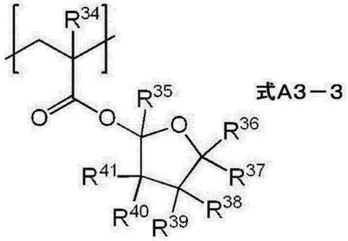
式A3-3中、R34は、水素原子、又はメチル基を表し、R35~R41は、それぞれ独立して、水素原子、又は炭素数1~4のアルキル基を表す。式A3-3中、R34は、水素原子であることが好ましい。式A3-3中、R35~R41は、水素原子であることが好ましい。
式A3で表される構成単位の好ましい具体例としては、下記の構成単位が例示できる。なお、下記の構成単位におけるR34は、水素原子、又はメチル基を表す。
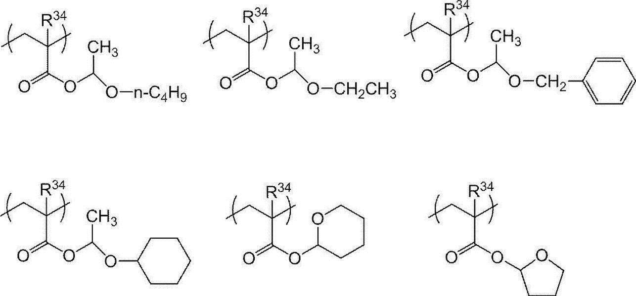
重合体Aは、1種の構成単位Aを有していてもよく、2種以上の構成単位Aを有していてもよい。
重合体Aにおける構成単位Aの含有比率は、重合体Aの全構成単位に対して、10モル%以上であることが好ましく、10モル%~90モル%であることがより好ましく、20モル%~70モル%であることが特に好ましい。重合体Aにおける構成単位Aの含有比率は、13C-NMR測定から常法により算出されるピーク強度の強度比により確認する。
重合体Aは、酸基を有する構成単位(以下、「構成単位B」ともいう。)を含むことが好ましい。重合体Aが構成単位Bを含むことで、パターン形成時の感度が良好となり、パターン露光後の現像工程においてアルカリ性の現像液に溶けやすくなり、現像時間の短縮化を図ることができる。
構成単位Bにおける酸基とは、pKaが12以下のプロトン解離性基を意味する。感度向上の観点から、酸基のpKaは、10以下であることが好ましく、6以下であることがより好ましい。また、酸基のpKaは、-5以上であることが好ましい。
構成単位Bにおける酸基としては、例えば、カルボキシ基、スルホンアミド基、ホスホン酸基、スルホン酸基、フェノール性水酸基、スルホニルイミド基等が挙げられる。上記の中でも、酸基は、カルボキシ基、又はフェノール性水酸基であることが好ましい。
重合体Aへの酸基を有する構成単位の導入は、酸基を有するモノマーを共重合させることで行うことができる。
構成単位Bは、スチレン化合物に由来する構成単位若しくはビニル化合物に由来する構成単位に対して酸基が置換した構成単位、又は、(メタ)アクリル酸に由来する構成単位であることがより好ましい。
構成単位Bは、パターン形成時の感度がより良好となるという観点からカルボキシ基を有する構成単位及びフェノール性水酸基を有する構成単位からなる群より選択される少なくとも1種の構成単位であることが好ましい。
重合体Aは、1種の構成単位Bを含んでいてもよく、2種以上の構成単位Bを含んでいてもよい。
重合体Aにおける構成単位Bの含有比率は、パターン形成性の観点から、重合体Aの全構成単位に対して、0.1モル%~20モル%であることが好ましく、0.5モル%~15モル%であることがより好ましく、1モル%~10モル%であることが特に好ましい。重合体Aにおける構成単位Bの含有比率は、13C-NMR測定から常法により算出されるピーク強度の強度比により確認する。
重合体Aは、本開示に係る導電性転写材料の効果を損なわない範囲で、既述の構成単位A及び構成単位B以外の、他の構成単位(以下、「構成単位C」ともいう。)を含んでいてもよい。
構成単位Cを形成するモノマーとしては、例えば、スチレン化合物、(メタ)アクリル酸アルキルエステル、(メタ)アクリル酸環状アルキルエステル、(メタ)アクリル酸アリールエステル、不飽和ジカルボン酸ジエステル、ビシクロ不飽和化合物、マレイミド化合物、不飽和芳香族化合物、共役ジエン系化合物、不飽和モノカルボン酸、不飽和ジカルボン酸、不飽和ジカルボン酸無水物、脂肪族環式骨格を有する不飽和化合物、その他の不飽和化合物等が挙げられる。
構成単位Cとしては、具体的には、スチレン、tert-ブトキシスチレン、メチルスチレン、α-メチルスチレン、アセトキシスチレン、メトキシスチレン、エトキシスチレン、クロロスチレン、ビニル安息香酸メチル、ビニル安息香酸エチル、(メタ)アクリル酸メチル、(メタ)アクリル酸エチル、(メタ)アクリル酸n-プロピル、(メタ)アクリル酸イソプロピル、(メタ)アクリル酸2-ヒドロキシエチル、(メタ)アクリル酸2-ヒドロキシプロピル、(メタ)アクリル酸ベンジル、(メタ)アクリル酸イソボルニル、アクリロニトリル、エチレングリコールモノアセトアセテートモノ(メタ)アクリレート等を重合して形成される構成単位が挙げられる。その他、特開2004-264623号公報の段落0021~段落0024に記載の化合物を重合して形成される構成単位を挙げることができる。
構成単位Cとしては、得られる導電性転写材料の電気特性を向上させる観点から、芳香環を有する構成単位及び脂肪族環式骨格を有する構成単位からなる群より選択される少なくとも1種の構成単位であることが好ましい。上記構成単位を形成するモノマーとして、例えば、スチレン、tert-ブトキシスチレン、メチルスチレン、α-メチルスチレン、ジシクロペンタニル(メタ)アクリレート、シクロヘキシル(メタ)アクリレート、イソボルニル(メタ)アクリレート、ベンジル(メタ)アクリレート等が挙げられる。上記の中でも、構成単位Cは、シクロヘキシル(メタ)アクリレート由来の構成単位であることが好ましい。
また、構成単位Cを形成するモノマーとしては、密着性の観点から、例えば、(メタ)アクリル酸アルキルエステルが好ましく、炭素数4~12のアルキル基を有する(メタ)アクリル酸アルキルエステルがより好ましい。具体的には、(メタ)アクリル酸メチル、(メタ)アクリル酸エチル、(メタ)アクリル酸プロピル、(メタ)アクリル酸n-ブチル、(メタ)アクリル酸2-エチルヘキシル等が挙げられる。
重合体Aは、1種の構成単位Cを含んでいてもよく、2種以上の構成単位Cを含んでいてもよい。
重合体Aにおける構成単位Cの含有比率は、重合体Aの全構成単位に対して、70モル%以下が好ましく、60質量%以下がより好ましく、50質量%以下が特に好ましい。重合体Aにおける構成単位Cの含有比率の下限値は、0モル%でもよい。重合体Aにおける構成単位Cの含有比率は、重合体Aの全構成単位に対して、1モル%以上であることが好ましく、5モル%以上であることがより好ましい。上記範囲であると、解像度及び密着性がより向上する。
重合体Aの重量平均分子量は、60,000以下であることが好ましい。重合体Aの重量平均分子量が60,000以下であることで、感光性樹脂層の溶融粘度を低く抑え、基板と貼り合わせる際において低温(例えば130℃以下)での貼り合わせを実現することができる。また、重合体Aの重量平均分子量は、2,000~60,000であることが好ましく、3,000~50,000であることがより好ましい。重合体Aの重量平均分子量は、既述の方法(すなわち、ゲルパーミエーションクロマトグラフィー)によって測定されるポリスチレン換算の重量平均分子量である。
ポジ型の感光性樹脂層は、1種の重合体Aを含有していてもよく、2種以上の重合体Aを含有していてもよい。
ポジ型の感光性樹脂層における重合体Aの含有量は、基板に対して良好な密着性を発現させる観点から、ポジ型の感光性樹脂層の全質量に対して、50質量%~99.9質量%であることが好ましく、70質量%~98質量%であることがより好ましい。
重合体Aの製造方法(合成法)は、制限されず、公知の方法を適用できる。重合体Aの製造方法としては、例えば、構成単位Aを形成するための重合性モノマー、さらに必要に応じて、酸基を有する構成単位Bを形成するための重合性モノマー、及び構成単位Cを形成するための重合性モノマーを、有機溶剤中、重合開始剤を用いて重合する方法が挙げられる。
-光酸発生剤-
ポジ型の感光性樹脂層は、光酸発生剤を含有することが好ましい。
ポジ型の感光性樹脂層は、光酸発生剤を含有することが好ましい。
光酸発生剤は、紫外線、遠紫外線、X線、荷電粒子線等の放射線を照射されることにより酸を発生することができる化合物である。光酸発生剤としては、波長300nm以上、好ましくは波長300nm~450nmの活性光線に感応し、酸を発生する化合物が好ましい。また、波長300nm以上の活性光線に直接感応しない光酸発生剤についても、増感剤と併用することによって波長300nm以上の活性光線に感応し、酸を発生する化合物であれば、増感剤と組み合わせて好ましく用いることができる。
光酸発生剤としては、pKaが4以下の酸を発生する光酸発生剤が好ましく、pKaが3以下の酸を発生する光酸発生剤がより好ましく、pKaが2以下の酸を発生する光酸発生剤が特に好ましい。pKaの下限値は特に定めない。pKaは、例えば、-10.0以上であることが好ましい。
光酸発生剤としては、例えば、イオン性光酸発生剤、及び非イオン性光酸発生剤が挙げられる。光酸発生剤は、感度及び解像度の観点から、後述するオニウム塩化合物、及び後述するオキシムスルホネート化合物からなる群より選択される少なくとも1種の化合物を含むことが好ましく、オキシムスルホネート化合物を含むことがより好ましい。
イオン性光酸発生剤としては、例えば、ジアリールヨードニウム塩化合物及びトリアリールスルホニウム塩化合物等のオニウム塩化合物、第四級アンモニウム塩化合物などが挙げられる。上記の中でも、イオン性光酸発生剤は、オニウム塩化合物であることが好ましく、トリアリールスルホニウム塩化合物、及びジアリールヨードニウム塩化合物の少なくとも一方であることがより好ましい。
イオン性光酸発生剤としては、特開2014-85643号公報の段落0114~0133に記載のイオン性光酸発生剤も好ましく用いることができる。
非イオン性光酸発生剤としては、例えば、トリクロロメチル-s-トリアジン化合物、ジアゾメタン化合物、イミドスルホネート化合物、オキシムスルホネート化合物等を挙げることができる。上記の中でも、非イオン性光酸発生剤は、感度、解像度、及び密着性の観点から、オキシムスルホネート化合物であることが好ましい。トリクロロメチル-s-トリアジン化合物、及びジアゾメタン化合物の具体例としては、特開2011-221494号公報の段落0083~段落0088に記載の化合物が例示できる。
オキシムスルホネート化合物、すなわち、オキシムスルホネート構造を有する化合物としては、下記式(B1)で表されるオキシムスルホネート構造を有する化合物が好ましい。

式(B1)中、R21は、アルキル基又はアリール基を表し、*は、他の原子又は他の基との結合部位を表す。
式(B1)で表されるオキシムスルホネート構造を有する化合物は、いずれの基も置換されてもよく、R21におけるアルキル基は、直鎖状であっても、分岐構造を有していても、環構造を有していてもよい。許容される置換基は以下に説明する。
R21で表されるアルキル基としては、炭素数1~10の、直鎖状又は分岐状アルキル基が好ましい。R21で表されるアルキル基は、炭素数6~11のアリール基、炭素数1~10のアルコキシ基、シクロアルキル基、又はハロゲン原子で置換されてもよい。
R21で表されるアリール基としては、炭素数6~18のアリール基が好ましく、フェニル基又はナフチル基がより好ましい。R21で表されるアリール基は、炭素数1~4のアルキル基、アルコキシ基及びハロゲン原子からなる群より選択される1つ以上の基で置換されてもよい。
ポジ型の感光性樹脂層は、1種の光酸発生剤を含有していてもよく、2種以上の光酸発生剤を含有していてもよい。
ポジ型の感光性樹脂層における光酸発生剤の含有量は、感度及び解像度の観点から、ポジ型の感光性樹脂層の全質量に対して、0.1質量%~10質量%であることが好ましく、0.5質量%~5質量%であることがより好ましい。
-他の成分A-
ポジ型の感光性樹脂層は、上記成分以外の成分(以下、「他の成分A」ともいう。)を含有していてもよい。他の成分Aは、制限されず、目的等に応じて適宜選択できる。他の成分としては、例えば、界面活性剤、後述する腐食防止剤等が挙げられる。
ポジ型の感光性樹脂層は、上記成分以外の成分(以下、「他の成分A」ともいう。)を含有していてもよい。他の成分Aは、制限されず、目的等に応じて適宜選択できる。他の成分としては、例えば、界面活性剤、後述する腐食防止剤等が挙げられる。
界面活性剤としては、例えば、アニオン系界面活性剤、カチオン系界面活性剤、ノニオン系(非イオン系)界面活性剤、及び両性界面活性剤が挙げられる。ポジ型の感光性樹脂層が界面活性剤を含有することで、膜厚の均一性を高めることができる。上記の中でも、界面活性剤は、ノニオン系界面活性剤であることが好ましい。
ノニオン系界面活性剤としては、例えば、ポリオキシエチレン高級アルキルエーテル系界面活性剤、ポリオキシエチレン高級アルキルフェニルエーテル系界面活性剤、ポリオキシエチレングリコールの高級脂肪酸ジエステル系界面活性剤、シリコーン系界面活性剤、フッ素系界面活性剤等が挙げられる。ノニオン系界面活性剤の具体例としては、KP(信越化学工業株式会社製)、ポリフロー(共栄社化学株式会社製)、エフトップ(JEMCO社製)、メガファック(登録商標、例えばメガファックF551A、DIC株式会社製)、フロラード(住友スリーエム株式会社製)、アサヒガード(登録商標、AGC株式会社製)、サーフロン(登録商標、AGCセイケミカル株式会社製)、PolyFox(OMNOVA社製)、サーフィノール(日信化学工業株式会社製)及び、SH-8400(東レ・ダウコーニング株式会社製)等の各シリーズが挙げられる。
ポジ型の感光性樹脂層は、1種の界面活性剤を含有していてもよく、2種以上の界面活性剤を含有していてもよい。
ポジ型の感光性樹脂層における界面活性剤の含有量は、膜厚の均一性の観点から、ポジ型の感光性樹脂層の全質量に対して、0.05質量%~10質量%であることが好ましく、0.05質量%~5質量%であることがより好ましい。
(ネガ型の感光性樹脂層)
ネガ型の感光性樹脂層は、制限されず、公知のネガ型の感光性樹脂層を適用できる。ネガ型の感光性樹脂層は、パターン形成性の観点から、重合性化合物、重合開始剤、及びバインダーポリマーを含有することが好ましい。
ネガ型の感光性樹脂層は、制限されず、公知のネガ型の感光性樹脂層を適用できる。ネガ型の感光性樹脂層は、パターン形成性の観点から、重合性化合物、重合開始剤、及びバインダーポリマーを含有することが好ましい。
-重合性化合物-
ネガ型の感光性樹脂層は、重合性化合物を含有することが好ましい。
ネガ型の感光性樹脂層は、重合性化合物を含有することが好ましい。
重合性化合物としては、重合可能な化合物、例えば、ラジカル重合性化合物、カチオン重合性化合物等が挙げられる。上記の中でも、重合性化合物は、光重合性化合物であることが好ましく、エチレン性不飽和化合物であることがより好ましい。エチレン性不飽和化合物は、1つ以上のエチレン性不飽和基を有する化合物である。エチレン性不飽和基としては、(メタ)アクリロイル基がより好ましい。エチレン性不飽和化合物としては、(メタ)アクリレート化合物が好ましい。
エチレン性不飽和化合物としては、2官能以上のエチレン性不飽和化合物を含むことが好ましい。ここで、2官能以上のエチレン性不飽和化合物とは、一分子中にエチレン性不飽和基を2つ以上有する化合物を意味する。
2官能のエチレン性不飽和化合物としては、例えば、トリシクロデカンジメタノールジ(メタ)アクリレート、1,9-ノナンジオールジ(メタ)アクリレート、1,6-ヘキサンジオールジ(メタ)アクリレート等が挙げられる。
2官能のエチレン性不飽和化合物としては、より具体的には、トリシクロデカンジメタノールジアクリレート(A-DCP、新中村化学工業(株)製)、トリシクロデカンジメタノールジメタクリレート(DCP、新中村化学工業(株)製)、1,9-ノナンジオールジアクリレート(A-NOD-N、新中村化学工業(株)製)、1,6-ヘキサンジオールジアクリレート(A-HD-N、新中村化学工業(株)製)、ポリテトラメチレングリコール#650ジアクリレート(A-PTMG-65、新中村化学工業(株)製)等が挙げられる。
3官能以上のエチレン性不飽和化合物としては、例えば、ジペンタエリスリトール(トリ/テトラ/ペンタ/ヘキサ)(メタ)アクリレート、ペンタエリスリトール(トリ/テトラ)(メタ)アクリレート、トリメチロールプロパントリ(メタ)アクリレート、ジトリメチロールプロパンテトラ(メタ)アクリレート、イソシアヌル酸(メタ)アクリレート、グリセリントリ(メタ)アクリレート骨格の(メタ)アクリレート化合物等が挙げられる。ここで、「(トリ/テトラ/ペンタ/ヘキサ)(メタ)アクリレート」との用語は、トリ(メタ)アクリレート、テトラ(メタ)アクリレート、ペンタ(メタ)アクリレート、及びヘキサ(メタ)アクリレートを包含する概念である。また、「(トリ/テトラ)(メタ)アクリレート」との用語は、トリ(メタ)アクリレート及びテトラ(メタ)アクリレートを包含する概念である。
エチレン性不飽和化合物は、現像性向上の観点から、酸基を有するエチレン性不飽和化合物を含むことが好ましい。酸基としては、例えば、リン酸基、スルホン酸基、カルボキシ基等が挙げられ、カルボキシ基が好ましい。
酸基を有するエチレン性不飽和化合物としては、例えば、酸基を有する3~4官能のエチレン性不飽和化合物、酸基を有する5~6官能のエチレン性不飽和化合物等が挙げられる。
カルボキシ基を有する2官能以上のエチレン性不飽和化合物としては、アロニックス(登録商標)TO-2349(東亞合成(株)製)、アロニックスM-520(東亞合成(株)製)、及びアロニックスM-510(東亞合成(株)製)が好ましい。
酸基を有するエチレン性不飽和化合物は、特開2004-239942号公報の段落0025~0030に記載の酸基を有する重合性化合物であることも好ましい。上記文献の内容は本明細書に組み込まれる。
ネガ型の感光性樹脂層は、1種の重合性化合物を含有していてもよく、2種以上の重合性化合物を含有していてもよい。
ネガ型の感光性樹脂層における重合性化合物の含有量は、感光性の観点から、ネガ型の感光性樹脂層の全質量に対して、1質量%~70質量%であることが好ましく、5質量%~70質量%であることがより好ましく、5質量%~60質量%であることがさらに好ましく、8質量%~50質量%であることが特に好ましい。
-重合開始剤-
ネガ型の感光性樹脂層は、重合開始剤を含有することが好ましい。
ネガ型の感光性樹脂層は、重合開始剤を含有することが好ましい。
重合開始剤としては、光重合開始剤、及び熱重合開始剤の少なくとも一方が好ましく、光重合開始剤がより好ましい。
光重合開始剤としては、例えば、オキシムエステル構造を有する光重合開始剤(以下、「オキシム系光重合開始剤」ともいう。)、α-アミノアルキルフェノン構造を有する光重合開始剤(以下、「α-アミノアルキルフェノン系光重合開始剤」ともいう。)、α-ヒドロキシアルキルフェノン構造を有する光重合開始剤(以下、「α-ヒドロキシアルキルフェノン系重合開始剤」ともいう。)、アシルフォスフィンオキサイド構造を有する光重合開始剤(以下、「アシルフォスフィンオキサイド系光重合開始剤」ともいう。)、N-フェニルグリシン構造を有する光重合開始剤(以下、「N-フェニルグリシン系光重合開始剤」ともいう。)等が挙げられる。
光重合開始剤は、オキシム系光重合開始剤、α-アミノアルキルフェノン系光重合開始剤、α-ヒドロキシアルキルフェノン系重合開始剤、及びN-フェニルグリシン系光重合開始剤からなる群より選択される少なくとも1種を含むことが好ましく、オキシム系光重合開始剤、α-アミノアルキルフェノン系光重合開始剤、及びN-フェニルグリシン系光重合開始剤からなる群より選択される少なくとも1種を含むことがより好ましい。
また、光重合開始剤としては、例えば、特開2011-95716号公報の段落0031~0042、特開2015-014783号公報の段落0064~0081に記載された光重合開始剤を用いてもよい。
光重合開始剤の市販品としては、例えば、1-[4-(フェニルチオ)フェニル]-1,2-オクタンジオン-2-(O-ベンゾイルオキシム)(商品名:IRGACURE(登録商標) OXE-01、BASF社製)、1-[9-エチル-6-(2-メチルベンゾイル)-9H-カルバゾール-3-イル]エタノン-1-(O-アセチルオキシム)(商品名:IRGACURE OXE-02、BASF社製)、2-(ジメチルアミノ)-2-[(4-メチルフェニル)メチル]-1-[4-(4-モルホリニル)フェニル]-1-ブタノン(商品名:IRGACURE 379EG、BASF社製)、2-メチル-1-(4-メチルチオフェニル)-2-モルフォリノプロパン-1-オン(商品名:IRGACURE 907、BASF社製)、2-ヒドロキシ-1-{4-[4-(2-ヒドロキシ-2-メチル-プロピオニル)ベンジル]フェニル}-2-メチルプロパン-1-オン(商品名:IRGACURE 127、BASF社製)、2-ベンジル-2-ジメチルアミノ-1-(4-モルフォリノフェニル)-1-ブタノン(商品名:IRGACURE 369、BASF社製)、2-ヒドロキシ-2-メチル-1-フェニルプロパン-1-オン(商品名:IRGACURE 1173、BASF社製)、1-ヒドロキシシクロヘキシルフェニルケトン(商品名:IRGACURE 184、BASF社製)、2,2-ジメトキシ-1,2-ジフェニルエタン-1-オン(商品名:IRGACURE 651、BASF社製)等が挙げられる。
ネガ型の感光性樹脂層は、1種の重合開始剤を含有していてもよく、2種以上の重合開始剤を含有していてもよい。
ネガ型の感光性樹脂層における重合開始剤の含有量は、ネガ型の感光性樹脂層の全質量に対して、0.1質量%以上が好ましく、0.2質量%以上がより好ましく、0.3質量%以上が特に好ましい。また、ネガ型の感光性樹脂層における重合開始剤の含有量は、ネガ型の感光性樹脂層の全質量に対して、10質量%以下が好ましく、5質量%以下がより好ましい。
-バインダーポリマー-
ネガ型の感光性樹脂層は、バインダーポリマーを含有することが好ましい。
ネガ型の感光性樹脂層は、バインダーポリマーを含有することが好ましい。
バインダーポリマーは、現像性の観点から、アルカリ可溶性樹脂であることが好ましい。アルカリ可溶性樹脂としては、酸価60mgKOH/g以上の樹脂であることが好ましく、酸価60mgKOH/g以上の、カルボキシ基を有する(メタ)アクリル樹脂(以下、「重合体B」ともいう。)であることがより好ましい。
本開示において、「アルカリ可溶性」とは、25℃の1mol/L水酸化ナトリウム溶液に可溶であることをいう。また、「可溶である」とは、100mLの溶媒に0.1g以上溶解することをいう。
本開示において、「酸価」とは、JIS K0070:1992に記載の方法にしたがって測定された値を意味する。
本開示において、「(メタ)アクリル樹脂」とは、(メタ)アクリル酸に由来する構成単位及び(メタ)アクリル酸エステルに由来する構成単位の少なくとも一方を含む樹脂を意味する。
重合体Bにおける(メタ)アクリル酸に由来する構成単位及び(メタ)アクリル酸エステルに由来する構成単位の合計割合は、重合体Bの全構成単位に対して、30モル%以上であることが好ましく、50モル%以上であることがより好ましい。
重合体Bは、カルボキシ基を有する構成単位を含む。重合体Bに含まれるカルボキシ基を有する構成単位は、1種であってもよく、2種以上であってもよい。
重合体Bにおけるカルボキシ基を有する構成単位の含有比率は、現像性の観点から、重合体Bの全構成単位に対して、5モル%~50モル%であることが好ましく、5モル%~40モル%であることがより好ましく、10モル%~40モル%であることがさらに好ましく、10モル%~30モル%であることが特に好ましい。
バインダーポリマー、特に重合体Bは、硬化後の透湿度及び強度の観点から、芳香環を有する構成単位を含むことが好ましい。芳香環を有する構成単位を形成するモノマーとしては、スチレン、tert-ブトキシスチレン、メチルスチレン、α-メチルスチレン等のスチレン化合物、ベンジル(メタ)アクリレートなどが挙げられる。芳香環を有する構成単位としては、スチレン化合物由来の構成単位であることが好ましい。
バインダーポリマー、特に重合体Bは、硬化後の強度の観点から、エチレン性不飽和基を有する構成単位を含むことが好ましい。アルカリ可溶性樹脂は、側鎖にエチレン性不飽和基を有する構成単位を含むことが好ましい。本開示において、「主鎖」とは樹脂を構成する高分子化合物の分子中で相対的に最も長い結合鎖を表し、「側鎖」とは主鎖から枝分かれしている原子団を表す。エチレン性不飽和基としては、(メタ)アクリル基が好ましく、(メタ)アクリロキシ基がより好ましい。
バインダーポリマーの酸価は、60mgKOH/g以上であることが好ましく、60mgKOH/g~200mgKOH/gであることがより好ましく、60mgKOH/g~150mgKOH/gであることがさらに好ましく、60mgKOH/g~130mgKOH/gであることが特に好ましい。
バインダーポリマーの重量平均分子量(Mw)は、3,000を超えることが好ましく、3,000を超え60,000以下であることがより好ましく、5,000~50,000であることが特に好ましい。バインダーポリマーの重量平均分子量は、以下の方法によって測定されるポリスチレン換算の重量平均分子量である。
重量平均分子量は、ゲルパーミエーションクロマトグラフィー(GPC)によって測定することができる。測定装置としては、様々な市販の装置を用いることができ、装置の内容、及び、測定技術は同当業者に公知である。GPCによる重量平均分子量の測定は、測定装置として、HLC(登録商標)-8220GPC(東ソー(株)製)を用い、カラムとして、TSKgel(登録商標)Super HZM-M(4.6mmID×15cm、東ソー(株)製)、Super HZ4000(4.6mmID×15cm、東ソー(株)製)、Super HZ3000(4.6mmID×15cm、東ソー(株)製)、Super HZ2000(4.6mmID×15cm、東ソー(株)製)をそれぞれ1本、直列に連結したものを用い、溶離液として、THF(テトラヒドロフラン)を用いることができる。また、測定条件としては、試料濃度を0.2質量%、流速を0.35mL/min、サンプル注入量を10μL、及び測定温度を40℃とし、示差屈折率(RI)検出器を用いて行うことができる。検量線は、東ソー(株)製の「標準試料TSK standard,polystyrene」:「F-40」、「F-20」、「F-4」、「F-1」、「A-5000」、「A-2500」及び「A-1000」の7サンプルのいずれかを用いて作製できる。
ネガ型の感光性樹脂層は、1種のバインダーポリマーを含有していてもよく、2種以上のバインダーポリマーを含有していてもよい。
ネガ型の感光性樹脂層におけるバインダーポリマーの含有量は、ネガ型の感光性樹脂層の全質量に対して、10質量%~90質量%であることが好ましく、20質量%~80質量%であることがより好ましく、30質量%~70質量%であることが特に好ましい。
-他の成分-
ネガ型の感光性樹脂層は、上記成分以外の成分(以下、「他の成分」ともいう。)を含有していてもよい。他の成分は、制限されず、目的等に応じて適宜選択できる。他の成分としては、例えば、熱架橋性化合物、増感剤、界面活性剤、後述する腐食防止剤等が挙げられる。
ネガ型の感光性樹脂層は、上記成分以外の成分(以下、「他の成分」ともいう。)を含有していてもよい。他の成分は、制限されず、目的等に応じて適宜選択できる。他の成分としては、例えば、熱架橋性化合物、増感剤、界面活性剤、後述する腐食防止剤等が挙げられる。
熱架橋性化合物としては、例えば、ブロックイソシアネート化合物、ビスフェノールA型のエポキシ化合物、クレゾールノボラック型のエポキシ化合物、ビフェニル型のエポキシ化合物、脂環式のエポキシ化合物、メラミン化合物等が挙げられる。ここで、「熱架橋性化合物」とは、熱により架橋反応を起こし得る官能基(すなわち、熱架橋性基)を1分子中に1つ以上有する化合物を意味する。
上記の中でも、熱架橋性化合物としては、ブロックイソシアネート化合物が好ましい。ここで、「ブロックイソシアネート化合物」とは、イソシアネートのイソシアネート基をブロック剤で保護(マスク)した構造を有する化合物を意味する。
ブロックイソシアネート化合物の解離温度は、100℃~160℃であることが好ましく、130℃~150℃であることがより好ましい。ここで、「ブロックイソシアネート化合物の解離温度」とは、示差走査熱量計(例えば、セイコーインスツルメンツ(株)製、DSC6200)を用いて、DSC(Differential scanning calorimetry)分析にて測定した場合に、ブロックイソシアネート化合物の脱保護反応に伴う吸熱ピークの温度を意味する。
解離温度が100℃~160℃であるブロック剤としては、例えば、ピラゾール化合物(例えば、3,5-ジメチルピラゾール、3-メチルピラゾール、4-ブロモ-3,5-ジメチルピラゾール、及び4-ニトロ-3,5-ジメチルピラゾール)、活性メチレン化合物(例えば、マロン酸ジエステル(例えば、マロン酸ジメチル、マロン酸ジエチル、マロン酸ジn-ブチル、及びマロン酸ジ2-エチルヘキシル))、トリアゾール化合物(例えば、1,2,4-トリアゾール)、オキシム化合物(例えば、ホルムアルドオキシム、アセトアルドオキシム、アセトオキシム、メチルエチルケトオキシム、シクロヘキサノンオキシム等の分子内に-C(=N-OH)-で表される構造を有する化合物)等が挙げられる。上記の中でも、保存安定性の観点から、オキシム化合物、又はピラゾール化合物が好ましく、オキシム化合物が特に好ましい。
ブロックイソシアネート化合物は、市販品であってもよい。例えば、カレンズAOI-BM、カレンズMOI-BM、カレンズMOI-BP(いずれも昭和電工(株)製)、ブロック型のデュラネートシリーズ(旭化成(株)製)等が挙げられる。
ブロックイソシアネート化合物の分子量は、200~3,000であることが好ましく、250~2,600であることがより好ましく、280~2,200であることが特に好ましい。
ネガ型の感光性樹脂層は、1種の熱架橋性化合物を含有していてもよく、2種以上の熱架橋性化合物を含有していてもよい。
ネガ型の感光性樹脂層における熱架橋性化合物の含有量は、得られる硬化膜(すなわち、ネガ型の感光性樹脂層の硬化物)の強度の観点から、ネガ型の感光性樹脂層の全質量に対して、1質量%~50質量%であることが好ましく、5質量%~30質量%であることがより好ましい。
増感剤としては、例えば、N-フェニルグリシン等が挙げられる。
ネガ型の感光性樹脂層は、1種の増感剤を含有していてもよく、2種以上の増感剤を含有していてもよい。
ネガ型の感光性樹脂層における増感剤の含有量は、ネガ型の感光性樹脂層の全質量に対して、0.01質量%~5質量%であることが好ましい。
界面活性剤としては、例えば、アニオン系界面活性剤、カチオン系界面活性剤、ノニオン系(非イオン系)界面活性剤、両性界面活性剤が挙げられる。ポジ型の感光性樹脂層が界面活性剤を含有することで、膜厚の均一性を高めることができる。上記の中でも、界面活性剤は、ノニオン系界面活性剤であることが好ましい。
ノニオン系界面活性剤としては、例えば、ポリオキシエチレン高級アルキルエーテル化合物、ポリオキシエチレン高級アルキルフェニルエーテル化合物、ポリオキシエチレングリコールの高級脂肪酸ジエステル化合物、シリコーン系、フッ素系等の界面活性剤が挙げられる。ノニオン系界面活性剤の具体例としては、KP(信越化学工業株式会社製)、ポリフロー(共栄社化学株式会社製)、エフトップ(JEMCO社製)、メガファック(登録商標、例えばメガファックF551A、DIC株式会社製)、フロラード(住友スリーエム株式会社製)、アサヒガード(登録商標、AGC株式会社製)、サーフロン(登録商標、AGCセイケミカル株式会社製)、PolyFox(OMNOVA社製)、サーフィノール(日信化学工業株式会社製)及びSH-8400(東レ・ダウコーニング株式会社製)等の各シリーズが挙げられる。
ネガ型の感光性樹脂層は、1種の界面活性剤を含有していてもよく、2種以上の界面活性剤を含有していてもよい。
ネガ型の感光性樹脂層における界面活性剤の含有量は、膜厚の均一性の観点から、ネガ型の感光性樹脂層の全質量に対して、0.05質量%~15質量%であることが好ましく、1質量%~15質量%であることがより好ましい。
(第1の樹脂層の形成方法)
第1の樹脂層の形成方法は、制限されず、公知の方法を適用できる。第1の樹脂層の形成方法としては、例えば、上記各成分を含む第1の樹脂層形成用塗布液を、被塗布物上に塗布し、乾燥させる方法が挙げられる。
第1の樹脂層の形成方法は、制限されず、公知の方法を適用できる。第1の樹脂層の形成方法としては、例えば、上記各成分を含む第1の樹脂層形成用塗布液を、被塗布物上に塗布し、乾燥させる方法が挙げられる。
塗布方法としては、例えば、スリット塗布、スピン塗布、カーテン塗布、インクジェット塗布等が挙げられる。
第1の樹脂層形成用塗布液は、上記各成分、及び溶剤を任意の割合で混合することによって調製できる。
溶剤は、制限されず、公知の溶剤を適用できる。溶剤としては、例えば、エチレングリコールモノアルキルエーテル系溶剤、エチレングリコールジアルキルエーテル系溶剤、エチレングリコールモノアルキルエーテルアセテート系溶剤、プロピレングリコールモノアルキルエーテル系溶剤、プロピレングリコールジアルキルエーテル系溶剤、プロピレングリコールモノアルキルエーテルアセテート系溶剤、ジエチレングリコールジアルキルエーテル系溶剤、ジエチレングリコールモノアルキルエーテルアセテート系溶剤、ジプロピレングリコールモノアルキルエーテル系溶剤、ジプロピレングリコールジアルキルエーテル系溶剤、ジプロピレングリコールモノアルキルエーテルアセテート系溶剤、エステル系溶剤、ケトン系溶剤、アミド系溶剤、ラクトン系溶剤等が挙げられる。
また、溶剤の好ましい例としては、以下に記載のエステル系溶剤、エーテル系溶剤、ケトン系溶剤等が挙げられる。
エステル系溶剤としては、酢酸エチル、酢酸プロピル、酢酸イソブチル、酢酸sec-ブチル、酢酸t-ブチル、酢酸イソプロピル、酢酸n-ブチル、1-メトキシ-2-プロピルアセテート等が挙げられる。
エーテル系溶剤としては、ジイソプロピルエーテル、1,4-ジオキサン、1,2-ジメトキシエタン、1,3-ジオキソラン、プロピレングリコールジメチルエーテル、プロピレングリコールモノエチルエーテル等が挙げられる。
ケトン系溶剤としては、メチルn-ブチルケトン、メチルエチルケトン、メチルイソブチルケトン、ジエチルケトン、メチルn-プロピルケトン、メチルイソプロピルケトン等が挙げられる。
エステル系溶剤としては、酢酸エチル、酢酸プロピル、酢酸イソブチル、酢酸sec-ブチル、酢酸t-ブチル、酢酸イソプロピル、酢酸n-ブチル、1-メトキシ-2-プロピルアセテート等が挙げられる。
エーテル系溶剤としては、ジイソプロピルエーテル、1,4-ジオキサン、1,2-ジメトキシエタン、1,3-ジオキソラン、プロピレングリコールジメチルエーテル、プロピレングリコールモノエチルエーテル等が挙げられる。
ケトン系溶剤としては、メチルn-ブチルケトン、メチルエチルケトン、メチルイソブチルケトン、ジエチルケトン、メチルn-プロピルケトン、メチルイソプロピルケトン等が挙げられる。
第1の樹脂層形成用塗布液中の固形分濃度は、制限されず、例えば、0.5質量%~40質量%の範囲で適宜設定できる。
[密着層]
本開示に係る導電性転写材料は、上記銀ナノワイヤーを含む層の、上記第1の樹脂層とは反対側の面上に、厚さが1nm~250nmである密着層を有することが好ましい。本開示に係る導電性転写材料は、上記銀ナノワイヤーを含む層の上記第1の樹脂層とは反対側の面上に、厚さが1nm~250nmである密着層を有することで、基板に対する密着性が高く、銀ナノワイヤー層と基板との間の導電性が向上する。
本開示に係る導電性転写材料は、上記銀ナノワイヤーを含む層の、上記第1の樹脂層とは反対側の面上に、厚さが1nm~250nmである密着層を有することが好ましい。本開示に係る導電性転写材料は、上記銀ナノワイヤーを含む層の上記第1の樹脂層とは反対側の面上に、厚さが1nm~250nmである密着層を有することで、基板に対する密着性が高く、銀ナノワイヤー層と基板との間の導電性が向上する。
図2は、本開示に係る導電性転写材料の層構成の一例を概略的に示している。図2に示す導電性転写材料110は、仮支持体10と、第1の樹脂層20と、銀ナノワイヤーを含む層30と、密着層40と、をこの順で有する。
密着層の厚さは、密着性及び導電性の観点から、1nm~250nmであることが好ましく、1nm~150nmであることがより好ましく、1nm~100nmであることが特に好ましい。密着層の厚さは、上記「銀ナノワイヤーを含む層」の項において説明した方法によって測定する。
密着層は、密着性の観点から、有機材料(例えば、有機樹脂)を含有する密着層(以下、「有機層」ともいう。)であることが好ましい。密着層は、パターン形成における残渣除去の観点から、アルカリ可溶性樹脂を含有することがより好ましい。
アルカリ可溶性樹脂としては、パターン形成における残渣除去の観点から、酸価20mgKOH/g以上の樹脂であることが好ましく、酸価20mgKOH/g以上の、カルボキシ基を有する(メタ)アクリル樹脂であることがより好ましい。酸価の測定方法は、上記のとおりである。
(メタ)アクリル樹脂中における(メタ)アクリル酸に由来する構成単位及び(メタ)アクリル酸エステルに由来する構成単位の合計割合は、(メタ)アクリル樹脂の全構成単位に対して、30モル%以上であることが好ましく、50モル%以上であることがより好ましい。
アルカリ可溶性樹脂の酸価は、パターン形成における残渣除去の観点から、20mgKOH/g以上であることが好ましく、45mgKOH/g~200mgKOH/gであることがより好ましく、50mgKOH/g以上~150mgKOH/gであることが特に好ましい。同様の理由により、アルカリ可溶性樹脂の酸価は、60mgKOH/g以上であってもよく、80mgKOH/g以上であってもよい。
カルボキシ基を有する(メタ)アクリル樹脂は、カルボキシ基を有する構成単位を含む。上記(メタ)アクリル樹脂に含まれるカルボキシ基を有する構成単位は、1種であってもよく、2種以上であってもよい。
カルボキシ基を有する(メタ)アクリル樹脂におけるカルボキシ基を有する構成単位の含有比率は、現像性の観点から、アルカリ可溶性樹脂の全構成単位に対して、3モル%~50モル%であることが好ましく、3モル%~40モル%であることがより好ましく、3モル%~35モル%であることが特に好ましい。
アルカリ可溶性樹脂は、芳香環を有する構成単位を含んでいてもよい。芳香環を有する構成単位を形成するモノマーとしては、例えば、スチレン、tert-ブトキシスチレン、メチルスチレン、α-メチルスチレン等のスチレン化合物、ベンジル(メタ)アクリレートなどが挙げられる。芳香環を有する構成単位としては、スチレン化合物由来の構成単位であることが好ましい。
アルカリ可溶性樹脂は、エチレン性不飽和基を有する構成単位を含んでいてもよい。アルカリ可溶性樹脂は、側鎖にエチレン性不飽和基を有する構成単位を含むことが好ましい。エチレン性不飽和基としては、(メタ)アクリル基が好ましく、(メタ)アクリロキシ基がより好ましい。
アルカリ可溶性樹脂の重量平均分子量は、3,000を超えることが好ましく、3,000を超え60,000以下であることがより好ましく、5,000~50,000であることが特に好ましい。アルカリ可溶性樹脂の重量平均分子量は、既述の方法(すなわち、ゲルパーミエーションクロマトグラフィー)ポリスチレン換算の重量平均分子量である。
アルカリ可溶性樹脂としては、上記「ネガ型の感光性樹脂層」の項において説明したアルカリ可溶性樹脂を適用することもできる。
密着層は、1種のアルカリ可溶性樹脂を含有していてもよく、2種以上のアルカリ可溶性樹脂を含有していてもよい。
密着層におけるアルカリ可溶性樹脂の含有量は、密着性及び現像性の観点から、密着層の全質量に対して、50質量%以上であることが好ましく、60質量%以上であることがより好ましく、80質量%以上であることが特に好ましい。密着層におけるアルカリ可溶性樹脂の含有量の上限は、制限されない。密着層におけるアルカリ可溶性樹脂の含有量は、密着層の全質量に対して、例えば、100質量%以下の範囲で適宜設定することができる。
密着層におけるアルカリ可溶性樹脂は、熱硬化性樹脂であってもよい。熱硬化性樹脂は、制限されず、公知の熱硬化性樹脂を適用できる。
また、密着層は、上記成分に加えて、上記「第1の樹脂層」の項において説明した他の成分を含有していてもよい。
波長400nm~700nmにおける密着層の最低透過率は、80%以上であることが好ましく、90%以上であることがより好ましい。透過率は、上記仮支持体の透過率の測定方法と同様の方法によって測定される。
密着層は、有機層であってもよく、アルカリ可溶性の密着層であってもよく、熱硬化性の密着層であってもよく、感光性の密着層であってもよい。アルカリ可溶性の密着層は、密着層の成分として、少なくともアルカリ可溶性樹脂によって構成される。熱硬化性の層は、密着層の成分として、少なくとも熱硬化性樹脂によって構成される。感光性の密着層としては、例えば、ネガ型感光性の密着層、及びポジ型感光性の密着層が挙げられる。熱硬化性の密着層、又は感光性の密着層は、アルカリ可溶性をさらに有していてもよい。
密着層と第1の樹脂層との組み合わせとしては、下記(a)~(f)にそれぞれ記載された組み合わせが好ましく、下記(a)~(e)にそれぞれ記載された組み合わせがより好ましい。
(a)密着層がアルカリ可溶性の密着層であり、第1の樹脂層がポジ型の感光性樹脂層である。
(b)密着層がアルカリ可溶性の密着層であり、第1の樹脂層がネガ型の感光性樹脂層である。
(c)密着層が熱硬化性の密着層であり、第1の樹脂層がポジ型の感光性樹脂層である。
(d)密着層が熱硬化性の密着層であり、第1の樹脂層がネガ型の感光性樹脂層である。
(e)密着層がネガ型感光性の密着層であり、第1の樹脂層がネガ型の感光性樹脂層である。
(f)密着層がポジ型感光性の密着層であり、第1の樹脂層がポジ型の感光性樹脂層である。
(a)密着層がアルカリ可溶性の密着層であり、第1の樹脂層がポジ型の感光性樹脂層である。
(b)密着層がアルカリ可溶性の密着層であり、第1の樹脂層がネガ型の感光性樹脂層である。
(c)密着層が熱硬化性の密着層であり、第1の樹脂層がポジ型の感光性樹脂層である。
(d)密着層が熱硬化性の密着層であり、第1の樹脂層がネガ型の感光性樹脂層である。
(e)密着層がネガ型感光性の密着層であり、第1の樹脂層がネガ型の感光性樹脂層である。
(f)密着層がポジ型感光性の密着層であり、第1の樹脂層がポジ型の感光性樹脂層である。
(密着層の形成方法)
密着層の形成方法は、制限されず、公知の方法を適用できる。密着層の形成方法としては、例えば、上記各成分を含む密着層形成用塗布液を、被塗布物上に塗布し、乾燥させる方法が挙げられる。
密着層の形成方法は、制限されず、公知の方法を適用できる。密着層の形成方法としては、例えば、上記各成分を含む密着層形成用塗布液を、被塗布物上に塗布し、乾燥させる方法が挙げられる。
塗布方法としては、例えば、スリット塗布、スピン塗布、カーテン塗布、インクジェット塗布等が挙げられる。
乾燥温度は、溶剤等の揮発性成分の種類に応じて適宜設定することができる。乾燥温度は、例えば、60℃~120℃の範囲で設定することができる。
密着層形成用塗布液は、上記各成分、及び溶剤を任意の割合で混合することによって調製できる。
溶剤としては、制限されず、例えば、上記「第1の樹脂層」の項において説明した溶剤が挙げられる。
密着層形成用塗布液中の固形分濃度は、制限されず、例えば、0.5質量%~10質量%の範囲で適宜設定できる。
[腐食防止剤]
本開示に係る導電性転写材料において、上記銀ナノワイヤーを含む層、上記第1の樹脂層、及び上記密着層からなる群より選択される少なくとも1つは、腐食防止剤を含有することが好ましい。銀ナノワイヤーを含む層、第1の樹脂層、及び密着層からなる群より選択される少なくとも1つが、腐食防止剤を含むことで、耐久性を向上できる。
本開示に係る導電性転写材料において、上記銀ナノワイヤーを含む層、上記第1の樹脂層、及び上記密着層からなる群より選択される少なくとも1つは、腐食防止剤を含有することが好ましい。銀ナノワイヤーを含む層、第1の樹脂層、及び密着層からなる群より選択される少なくとも1つが、腐食防止剤を含むことで、耐久性を向上できる。
腐食防止剤は、制限されず、公知の腐食防止剤を適用できる。腐食防止剤としては、例えば、窒素原子及び硫黄原子の少なくとも1つを含有する化合物等が挙げられる。腐食防止剤は、耐久性の観点から、窒素原子及び硫黄原子の少なくとも1つを含有する複素環式化合物であることが好ましく、1つ以上の窒素原子を含有する5員環構造を含む化合物であることがより好ましく、トリアゾール構造を含む化合物、ベンゾイミダゾール構造を含む化合物、及びチアジアゾール構造を含む化合物からなる群より選択される少なくとも1種の化合物であることが特に好ましい。1つ以上の窒素原子を含有する5員環構造は、単環の構造であってもよく、縮合環を構成する部分構造であってもよい。
腐食防止剤の具体例としては、ベンゾイミダゾール、1,2,4-トリアゾール、ベンゾトリアゾール、トリルトリアゾール、ブチルベンジルトリアゾール、アルキルジチオチアジアゾール、アルキルチオール、2-アミノピリミジン、5,6-ジメチルベンゾイミダゾール、2-アミノ-5-メルカプト-1,3,4-チアジアゾール、2,5-ジメルカプト-1,3,4-チアジアゾール、2-メルカプトピリミジン、2-メルカプトベンゾオキサゾール、2-メルカプトベンゾチアゾール、2-メルカプトベンゾイミダゾール等が挙げられる。上記の中でも、腐食防止剤は、ベンゾイミダゾール、1,2,4-トリアゾール、及び2,5-ジメルカプト-1,3,4-チアジアゾールからなる群より選択される少なくとも1種の腐食防止剤であることが好ましい。
銀ナノワイヤーを含む層、第1の樹脂層、及び密着層は、それぞれ、1種の腐食防止剤を含有していてもよく、2種以上の腐食防止剤を含有していてもよい。
腐食防止剤の含有量は、銀ナノワイヤーを含む層、第1の樹脂層、及び密着層のうち、腐食防止剤を含有する層の全質量に対して、0.01質量%~8質量%であることが好ましい。
[光安定化剤]
本開示に係る導電性転写材料において、上記銀ナノワイヤーを含む層、上記第1の樹脂層、及び上記密着層からなる群より選択される少なくとも1つは、光安定化剤を含有することが好ましい。銀ナノワイヤーを含む層、第1の樹脂層、及び密着層からなる群より選択される少なくとも1つが、光安定化剤を含むことで、銀ナノワイヤー等の耐光性を向上できる。
本開示に係る導電性転写材料において、上記銀ナノワイヤーを含む層、上記第1の樹脂層、及び上記密着層からなる群より選択される少なくとも1つは、光安定化剤を含有することが好ましい。銀ナノワイヤーを含む層、第1の樹脂層、及び密着層からなる群より選択される少なくとも1つが、光安定化剤を含むことで、銀ナノワイヤー等の耐光性を向上できる。
光安定化剤は、制限されず、公知の光安定化剤を適用できる。光安定化剤としては、例えば、米国特許出願公開第2015/0270024号明細書の段落0032~段落0043に記載の化合物を使用できる。
光安定化剤の具体例としては、Fe、Co、Mn、V等の遷移金属化合物が挙げられる。遷移金属化合物に含まれる配位子としては、例えば、アセチルアセトナト(以下、「acac」ともいう。)、シクロペンタジエニル、ビピリジン、フェナントロリン、SO4
2-、NO3
-等が挙げられる。遷移金属化合物の具体例としては、フェロセン、Fe(acac)3、Co(acac)3、Mn(acac)3、VO(acac)3、アスコルビン酸鉄、硫酸鉄、トリス(2,2’-ビピリジン)硫酸鉄等が挙げられる。
銀ナノワイヤーを含む層、第1の樹脂層、及び密着層は、それぞれ、1種の光安定化剤を含有していてもよく、2種以上の光安定化剤を含有していてもよい。
光安定化剤の含有量は、銀ナノワイヤーを含む層、第1の樹脂層、及び密着層のうち、光安定化剤を含有する層の全質量に対して、0.01質量%~10質量%であることが好ましい。
[不純物]
本開示に係る導電性転写材料において、上記銀ナノワイヤーを含む層、上記第1の樹脂層、及び上記密着層の不純物の含有量が少ないことが好ましい。
不純物の具体例としては、ナトリウム、カリウム、マグネシウム、カルシウム、鉄、マンガン、銅、アルミニウム、チタン、クロム、コバルト、ニッケル、亜鉛、スズ、及びこれらのイオン、並びに、遊離ハロゲン、ハロゲン化物イオン(塩化物イオン、臭化物イオン、ヨウ化物イオン等)などが挙げられる。
各層における不純物の含有量は、質量基準で、1000ppm以下が好ましく、200ppm以下がより好ましく、40ppm以下がさらに好ましい。下限は特に定めるものではないが、現実的に減らせる限界及び測定限界の観点から、質量基準で、10ppb以上とすることができ、100ppb以上とすることができる。
不純物を上記範囲に減らす方法としては、各層の原料に不純物を含まないものを選択すること、及び層の形成時に不純物の混入を防ぐこと等が挙げられる。このような方法により、不純物量を上記範囲内とすることができる。
不純物は、例えば、ICP(Inductively Coupled Plasma)発光分光分析法、原子吸光分光法等の公知の方法で定量することができる。
本開示に係る導電性転写材料において、上記銀ナノワイヤーを含む層、上記第1の樹脂層、及び上記密着層の不純物の含有量が少ないことが好ましい。
不純物の具体例としては、ナトリウム、カリウム、マグネシウム、カルシウム、鉄、マンガン、銅、アルミニウム、チタン、クロム、コバルト、ニッケル、亜鉛、スズ、及びこれらのイオン、並びに、遊離ハロゲン、ハロゲン化物イオン(塩化物イオン、臭化物イオン、ヨウ化物イオン等)などが挙げられる。
各層における不純物の含有量は、質量基準で、1000ppm以下が好ましく、200ppm以下がより好ましく、40ppm以下がさらに好ましい。下限は特に定めるものではないが、現実的に減らせる限界及び測定限界の観点から、質量基準で、10ppb以上とすることができ、100ppb以上とすることができる。
不純物を上記範囲に減らす方法としては、各層の原料に不純物を含まないものを選択すること、及び層の形成時に不純物の混入を防ぐこと等が挙げられる。このような方法により、不純物量を上記範囲内とすることができる。
不純物は、例えば、ICP(Inductively Coupled Plasma)発光分光分析法、原子吸光分光法等の公知の方法で定量することができる。
また、各層における、ベンゼン、ホルムアルデヒド、トリクロロエチレン、1,3-ブタジエン、四塩化炭素、クロロホルム、N,N-ジメチルホルムアミド、N,N-ジメチルアセトアミド、ヘキサン等の化合物の含有量が少ないことが好ましい。これら化合物の各層中における含有量としては、質量基準で、1000ppm以下が好ましく、200ppm以下がより好ましく、40ppm以下がさらに好ましい。下限は特に定めるものではないが、現実的に減らせる限界及び測定限界の観点から、質量基準で、10ppb以上とすることができ、100ppb以上とすることができる。
化合物の不純物は、上記の金属の不純物と同様の方法で含有量を抑制することができる。また、公知の測定法により定量することができる
化合物の不純物は、上記の金属の不純物と同様の方法で含有量を抑制することができる。また、公知の測定法により定量することができる
[第2の樹脂層]
本開示に係る導電性転写材料は、上記仮支持体と上記第1の樹脂層との間に、第2の樹脂層を有することが好ましい。第2の樹脂層は、導電性転写材料を基板に貼り合わせる際に、いわゆるクッション層として機能し得るため、導電性転写材料の転写性を向上できる。また、第2の樹脂層は、現像処理によって除去され得るものであってもよく、仮支持体の剥離とともに第1の樹脂層から剥離され得るものであってもよい。
本開示に係る導電性転写材料は、上記仮支持体と上記第1の樹脂層との間に、第2の樹脂層を有することが好ましい。第2の樹脂層は、導電性転写材料を基板に貼り合わせる際に、いわゆるクッション層として機能し得るため、導電性転写材料の転写性を向上できる。また、第2の樹脂層は、現像処理によって除去され得るものであってもよく、仮支持体の剥離とともに第1の樹脂層から剥離され得るものであってもよい。
図3は、本開示に係る導電性転写材料の層構成の一例を概略的に示している。図3に示す導電性転写材料120は、仮支持体10と、第2の樹脂層50と、第1の樹脂層20と、銀ナノワイヤーを含む層30と、密着層40と、をこの順で有する。
第2の樹脂層は、バインダーポリマーを含有する。バインダーポリマーは、制限されず、転写性等を考慮して公知のバインダーポリマーから適宜選択できる。バインダーポリマーとしては、例えば、熱可塑性樹脂、アルカリ可溶性樹脂等が挙げられる。
熱可塑性樹脂は、制限されず、公知の熱可塑性樹脂を適用できる。熱可塑性樹脂としては、例えば、低密度ポリエチレン、中密度ポリエチレン、高密度ポリエチレン、ポリプロピレン等が挙げられる。
アルカリ可溶性樹脂は、制限されず、公知の熱可塑性樹脂を適用できる。アルカリ可溶性樹脂としては、例えば、上記「第1の樹脂層」及び「密着層」の項において説明したアルカリ可溶性樹脂等が挙げられる。
上記の中でも、バインダーポリマーは、現像性の観点から、アルカリ可溶性樹脂であることが好ましい。アルカリ可溶性樹脂は、酸価60mgKOH/g以上の樹脂であることが好ましく、酸価60mgKOH/g以上の、カルボキシ基を有する(メタ)アクリル樹脂であることがより好ましい。アルカリ可溶性樹脂の好ましい実施形態は、上記「第1の樹脂層」において説明したアルカリ可溶性樹脂と同様である。また、酸価の測定方法は、上記のとおりである。
第2の樹脂層は、他の成分として、可塑剤、界面活性剤等を含有していてもよい。
可塑剤は、制限されず、公知の可塑剤を適用できる。第2の樹脂層が可塑剤を含有することによって、本開示に係る導電性転写材料の転写性が向上する。可塑剤としては、市販品であってもよく、例えば、BPE-500(新中村化学工業(株)製)、UC-3510(東亞合成(株)製)等が挙げられる。
第2の樹脂層は、1種の可塑剤を含有していてもよく、2種以上の可塑剤を含有していてもよい。
可塑剤の含有量は、第2の樹脂層の全質量に対して、10質量%~30質量%であることが好ましい。
界面活性剤としては、例えば、上記「第1の樹脂層」の項において説明した界面活性剤が挙げられる。
第2の樹脂層は、1種の界面活性剤を含有していてもよく、2種以上の界面活性剤を含有していてもよい。
界面活性剤の含有量は、第2の樹脂層の全質量に対して、0.1質量%~5質量%であることが好ましい。
第2の樹脂層の厚さは、転写性の観点から、1μm~10μmであることが好ましく、3μm~10μmであることがより好ましい。第2の樹脂層の厚さは、上記「銀ナノワイヤーを含む層」の項において説明した方法によって測定する。
(第2の樹脂層の形成方法)
第2の樹脂層の形成方法は、制限されず、公知の方法を適用できる。第2の樹脂層の形成方法としては、例えば、上記各成分を含む第2の樹脂層形成用塗布液を、被塗布物上に塗布し、乾燥させる方法が挙げられる。
第2の樹脂層の形成方法は、制限されず、公知の方法を適用できる。第2の樹脂層の形成方法としては、例えば、上記各成分を含む第2の樹脂層形成用塗布液を、被塗布物上に塗布し、乾燥させる方法が挙げられる。
塗布方法としては、例えば、スリット塗布、スピン塗布、カーテン塗布、インクジェット塗布等が挙げられる。
乾燥温度は、溶剤等の揮発性成分の種類に応じて適宜設定することができる。乾燥温度は、例えば、60℃~120℃の範囲で設定することができる。
第2の樹脂層形成用塗布液は、上記各成分、及び溶剤を任意の割合で混合することによって調製できる。
溶剤としては、制限されず、例えば、上記「第1の樹脂層」の項において説明した溶剤が挙げられる。
第2の樹脂層形成用塗布液中の固形分濃度は、制限されず、例えば、1質量%~40質量%の範囲で適宜設定できる。
[中間層]
本開示に係る導電性転写材料は、上記仮支持体と上記第1の樹脂層との間に、第2の樹脂層以外の中間層を有していてもよい。本開示に係る転写フィルムが第2の樹脂層を有する場合、中間層は、第1の樹脂層と第2の樹脂層との間に配置されることが好ましい。
本開示に係る導電性転写材料は、上記仮支持体と上記第1の樹脂層との間に、第2の樹脂層以外の中間層を有していてもよい。本開示に係る転写フィルムが第2の樹脂層を有する場合、中間層は、第1の樹脂層と第2の樹脂層との間に配置されることが好ましい。
中間層としては、特開2005-259138号公報の段落0084~0087に記載の中間層を用いることができる。中間層としては、水又はアルカリ水溶液に、分散又は溶解するものが好ましい。
中間層に用いられる材料としては、例えば、ポリビニルアルコール、ポリビニルピロリドン、セルロース、ポリアクリルアミド、ポリエチレンオキサイド、ゼラチン、ポリビニルエーテル、ポリアミド、及びこれらの共重合体等が挙げられる。上記の中でも、ポリビニルアルコール及びポリビニルピロリドンが好ましい。
中間層の厚さは、0.5μm~10μmであることが好ましく、0.5μm~4μmであることがより好ましい。中間層の厚さは、上記「銀ナノワイヤーを含む層」の項において説明した方法によって測定する。
(中間層の形成方法)
中間層の形成方法は、制限されず、公知の方法を適用できる。中間層の形成方法としては、例えば、上記各成分を含む中間層形成用塗布液を、被塗布物上に塗布し、乾燥させる方法が挙げられる。
中間層の形成方法は、制限されず、公知の方法を適用できる。中間層の形成方法としては、例えば、上記各成分を含む中間層形成用塗布液を、被塗布物上に塗布し、乾燥させる方法が挙げられる。
塗布方法としては、例えば、スリット塗布、スピン塗布、カーテン塗布、インクジェット塗布等が挙げられる。
乾燥温度は、溶剤等の揮発性成分の種類に応じて適宜設定することができる。乾燥温度は、例えば、60℃~120℃の範囲で設定することができる。
中間層形成用塗布液は、上記各成分、及び溶剤を任意の割合で混合することによって調製できる。
溶剤としては、制限されず、例えば、上記「第1の樹脂層」の項において説明した溶剤が挙げられる。
中間層形成用塗布液中の固形分濃度は、制限されず、例えば、0.5質量%~30質量%の範囲で適宜設定できる。
[保護フィルム]
本開示に係る導電性転写材料は、仮支持体が配置された側とは反対側の最外層に位置に、保護フィルムを有していてもよい。
本開示に係る導電性転写材料は、仮支持体が配置された側とは反対側の最外層に位置に、保護フィルムを有していてもよい。
保護フィルムとしては、耐熱性及び耐溶剤性を有する樹脂フィルムを用いることができる。保護フィルムとしては、例えば、ポリオレフィンフィルム(例えば、ポリプロピレンフィルム、及びポリエチレンフィルム)、及びポリエステルフィルム(例えば、ポリエチレンテレフタレートフィルム)が挙げられる。また、保護フィルムとして、上述の支持体フィルムと同じ材料で構成された樹脂フィルムを用いてもよい。
保護フィルムの厚さは、1μm~100μmであることが好ましく、5μm~50μmであることがより好ましく、5μm~40μmであることが更に好ましく、15μm~30μmであることが特に好ましい。保護フィルムの厚さは、機械的強度に優れる点で1μm以上であることが好ましく、比較的安価となる点で100μm以下であることが好ましい。
保護フィルムと銀ナノワイヤーを含む層又は密着層との間の接着力は、保護フィルムを銀ナノワイヤーを含む層又は密着層から剥離し易くするため、仮支持体と銀ナノワイヤーを含む層又は密着層との間の接着力よりも小さいことが好ましい。
また、保護フィルムは、保護フィルム中に含まれる直径80μm以上のフィッシュアイ数が5個/m2以下であることが好ましい。なお、「フィッシュアイ」とは、種々の方法(例えば、材料の熱溶融、混練、押出、2軸延伸、及びキャスティング)によりフィルムを製造する際に、材料の異物、未溶解物、酸化劣化物等がフィルム中に取り込まれたものである。
保護フィルムに含まれる直径3μm以上の粒子の数は、30個/mm2以下であることが好ましく、10個/mm2以下であることがより好ましく、5個/mm2以下であることが更に好ましい。これにより、保護フィルムに含まれる粒子に起因する凹凸が感光性樹脂層又は導電層に転写されることにより生じる欠陥を抑制することができる。
保護フィルムにおいて、巻き取り性を付与する観点から、銀ナノワイヤーを含む層又は密着層と接する面とは反対側の表面の算術平均粗さRaは、0.01μm以上であることが好ましく、0.02μm以上であることがより好ましく、0.03μm以上であることが更に好ましい。一方で、上記算術平均粗さRaは、0.50μm未満であることが好ましく、0.40μm以下であることがより好ましく、0.30μm以下であることがさらに好ましい。
保護フィルムにおいて、転写時の欠陥抑制の観点から、銀ナノワイヤーを含む層又は密着層と接する面の表面粗さRaは、0.01μm以上であることが好ましく、0.02μm以上であることがより好ましく、0.03μm以上であることが更に好ましい。一方で、上記表面粗さRaは、0.50μm未満であることが好ましく、0.40μm以下であることがより好ましく、0.30μm以下であることが更に好ましい。
<パターンつき基板の製造方法>
本開示に係るパターンつき基板の製造方法は、上記導電性転写材料、及び基板を貼り合わせる工程(以下、「貼り合わせ工程」ともいう。)と、上記導電性転写材料における感光性樹脂層をパターン露光する工程(以下、「露光工程」ともいう。)と、上記パターン露光を経た導電性転写材料を現像してパターンを形成する工程(以下、「現像工程」ともいう。)と、をこの順に含む。本開示に係るパターンつき基板の製造方法は、上記工程を含むことで、パターンによって生じる段差を低くできるため、パターンとパターン上に積層される層との密着界面における面状異常の発生を抑制できる。
本開示に係るパターンつき基板の製造方法は、上記導電性転写材料、及び基板を貼り合わせる工程(以下、「貼り合わせ工程」ともいう。)と、上記導電性転写材料における感光性樹脂層をパターン露光する工程(以下、「露光工程」ともいう。)と、上記パターン露光を経た導電性転写材料を現像してパターンを形成する工程(以下、「現像工程」ともいう。)と、をこの順に含む。本開示に係るパターンつき基板の製造方法は、上記工程を含むことで、パターンによって生じる段差を低くできるため、パターンとパターン上に積層される層との密着界面における面状異常の発生を抑制できる。
[貼り合わせ工程]
本開示に係るパターンつき基板の製造方法は、上記導電性転写材料、及び基板を貼り合わせる工程を含む。
本開示に係るパターンつき基板の製造方法は、上記導電性転写材料、及び基板を貼り合わせる工程を含む。
導電性転写材料としては、上記導電性転写材料のうち、感光性樹脂層を有する導電性転写材料を適用することができる。感光性樹脂層は、上記「導電性転写材料」の項において説明したとおりであり、好ましい範囲も同様である。
貼り合わせ工程に適用可能な導電性転写材料の具体例としては、仮支持体と、厚さが1nm~300nmである感光性樹脂層と、銀ナノワイヤーを含む層と、をこの順で有する導電性転写材料等が挙げられる。貼り合わせ工程に適用可能な導電性転写材料における感光性樹脂層は、耐薬品性、及び耐久性の観点から、ネガ型の感光性樹脂層であることが好ましい。
基板は、ガラス、シリコン、フィルム等の基材自体が基板であってもよく、ガラス、シリコン、フィルム等の基材上に、必要により導電層などの任意の層が設けられた基板であってもよい。基板が導電層をさらに有する場合、基板は、基材上に導電層を有することが好ましい。
基材は、ガラス基材又はフィルム基材であることが好ましく、フィルム基材であることがより好ましく、樹脂フィルムであることが特に好ましい。
基材は、透明であることが好ましい。透明の基材としては、特開2010-86684号公報、特開2010-152809号公報及び特開2010-257492号公報に用いられている材料を好ましく用いることができる。また、基材の屈折率は、1.50~1.52であることが好ましい。
基材は、ガラス基材等の透光性基材で構成されていてもよく、コーニング社のゴリラガラスに代表される強化ガラス等を用いることができる。
基材としてフィルム基材を用いる場合、光学的に歪みが小さい基材、及び透明度が高い基材を用いることがより好ましく、樹脂フィルムを用いることが特に好ましい。
樹脂フィルムを構成する樹脂としては、例えば、ポリエチレンテレフタレート(PET)、ポリエチレンナフタレート、ポリカーボネート、トリアセチルセルロース、シクロオレフィンポリマー等が挙げられる。
導電層としては、例えば、金属層、導電性金属酸化物層等が挙げられる。ここで、「導電性」とは、体積抵抗率が1×10⁶Ωcm未満であることを意味する。体積抵抗率は、1×10⁴Ωcm未満であることが好ましい。
金属層を構成する金属としては、Al(アルミニウム)、Zn(亜鉛)、Cu(銅)、Fe(鉄)、Ni(ニッケル)、Cr(クロム)、Mo(モリブデン)等が挙げられる。金属層を構成する金属は、1種の金属元素からなる単体の金属であってもよく、2種以上の金属元素を含む金属であってもよく、少なくとも1種の金属元素を含む合金であってもよい。
導電性金属酸化物層を構成する導電性金属酸化物としては、ITO(Indium Tin Oxide)、IZO(Indium Zinc Oxide)、SiO2等が挙げられる。
導電層は、導電性及び細線形成性の観点から、金属層及び導電性金属酸化物層からなる群より選択される少なくとも1種の層であることが好ましく、金属層であることがより好ましく、銅層であることが特に好ましい。
導電層としては、静電容量型タッチパネルに用いられる視認部のセンサーに相当する電極パターン又は周辺取り出し部の配線であることが好ましい。
貼り合わせ工程においては、例えば、導電性転写材料及び基板を、導電性転写材料における銀ナノワイヤーを含む層(導電性転写材料が密着層を有する場合には密着層)と基板とを接触させることによって、貼り合わせる。
導電性転写材料及び基板の貼り合わせ(以下、「ラミネート」ともいう。)は、真空ラミネーター、オートカットラミネーター等の公知のラミネーターを用いて行うことができる。
ラミネート温度は、80℃~150℃であることが好ましく、90℃~150℃であることがより好ましく、100℃~150℃であることが特に好ましい。ゴムローラーを備えたラミネーターを用いる場合、ラミネート温度とは、ゴムローラー温度を指す。
ラミネート時の基板温度としては、例えば、10℃~150℃が挙げられ、20℃~150℃が好ましく、30℃~150℃がより好ましい。基板として樹脂基板を用いる場合には、ラミネート時の基板温度は、10℃~80℃が好ましく、20℃~60℃がより好ましく、30℃~50℃が特に好ましい。
ラミネート時の線圧は、0.5N/cm~20N/cmであることが好ましく、1N/cm~10N/cmであることがより好ましく、1N/cm~5N/cmであることが特に好ましい。
ラミネート時の搬送速度(ラミネート速度)は、0.5m/分~5m/分であることが好ましく、1.5m/分~3m/分であることがより好ましい。
[露光工程]
本開示に係るパターンつき基板の製造方法は、上記導電性転写材料における感光性樹脂層をパターン露光する工程を含む。パターン露光工程においては、導電性転写材料における感光性樹脂層をパターン露光することによって、感光性樹脂層に露光部及び非露光部を形成する。
本開示に係るパターンつき基板の製造方法は、上記導電性転写材料における感光性樹脂層をパターン露光する工程を含む。パターン露光工程においては、導電性転写材料における感光性樹脂層をパターン露光することによって、感光性樹脂層に露光部及び非露光部を形成する。
露光工程においては、導電性転写材料における感光性樹脂層がポジ型である場合、露光された感光性樹脂層(すなわち、露光部)は、極性変化によって現像液への溶解性が増大する。導電性転写材料における感光性樹脂層がネガ型である場合、露光された感光性樹脂層(すなわち、露光部)は、硬化する。
パターン露光の方法は、マスク(「フォトマスク」ともいう。)を介した露光であってもよく、レーザー等を用いたデジタル露光であってもよい。
露光の光源は、制限されず、感光性樹脂層の成分に応じて適宜選択できる。例えば、感光性樹脂層がポジ型である場合、光源としては、露光部が現像液に溶解し得る波長域の光(例えば、365nm、405nmなど)を照射できる光源が挙げられる。また、例えば、感光性樹脂層がネガ型である場合、光源としては、露光部が硬化し得る波長域の光(例えば、365nm又は405nm)を照射できる光源が挙げられる。光源の具体例としては、各種レーザー、発光ダイオード(LED)、超高圧水銀灯、高圧水銀灯、メタルハライドランプ等が挙げられる。
露光量は、5mJ/cm2~200mJ/cm2であることが好ましく、10mJ/cm2~200mJ/cm2であることがより好ましい。
露光工程においては、基板に貼り合わされた導電性転写材料から仮支持体を剥離した後、感光性樹脂層をパターン露光してもよく、仮支持体を残したまま、感光性樹脂層をパターン露光してもよい。
[現像工程]
本開示に係るパターンつき基板の製造方法は、上記パターン露光を経た導電性転写材料を現像してパターンを形成する工程を含む。
本開示に係るパターンつき基板の製造方法は、上記パターン露光を経た導電性転写材料を現像してパターンを形成する工程を含む。
現像工程においては、導電性転写材料における感光性樹脂層がポジ型である場合、導電性転写材料の露光部を現像液によって除去することで、パターンを形成できる。また、導電性転写材料における感光性樹脂層がネガ型である場合、導電性転写材料の非露光部を現像液によって除去することで、パターンを形成できる。
現像液は、制限されず、特開平5-72724号公報に記載の現像液等の公知の現像液を適用できる。
現像液は、アルカリ性水溶液であることが好ましい。アルカリ性水溶液に含有され得るアルカリ性化合物としては、例えば、水酸化ナトリウム、水酸化カリウム、炭酸ナトリウム、炭酸カリウム、炭酸水素ナトリウム、炭酸水素カリウム、テトラメチルアンモニウムヒドロキシド、テトラエチルアンモニウムヒドロキシド、テトラプロピルアンモニウムヒドロキシド、テトラブチルアンモニウムヒドロキシド、コリン(2-ヒドロキシエチルトリメチルアンモニウムヒドロキシド)等が挙げられる。
アルカリ性水溶液の25℃におけるpHとしては、8~13が好ましく、9~12がより好ましく、10~12が特に好ましい。
アルカリ性水溶液中におけるアルカリ性化合物の含有量は、アルカリ性水溶液全量に対し、0.1質量%~5質量%が好ましく、0.1質量%~3質量%がより好ましい。
現像液の液温度は、20℃~40℃が好ましい。
現像の方式としては、例えば、パドル現像、シャワー現像、シャワー及びスピン現像、ディップ現像等が挙げられる。
<積層体>
本開示に係る積層体は、基板と、銀ナノワイヤーを含む層と、厚さが1nm~300nmである第1の樹脂層と、をこの順で有する。本開示に係る積層体は、基板と、銀ナノワイヤーを含む層と、厚さが1nm~300nmである第1の樹脂層と、をこの順で有することで、パターンによって生じる段差を低くできるため、パターンを有する積層体上に更に層を積層する際の面状異常の発生を抑制できる。
本開示に係る積層体は、基板と、銀ナノワイヤーを含む層と、厚さが1nm~300nmである第1の樹脂層と、をこの順で有する。本開示に係る積層体は、基板と、銀ナノワイヤーを含む層と、厚さが1nm~300nmである第1の樹脂層と、をこの順で有することで、パターンによって生じる段差を低くできるため、パターンを有する積層体上に更に層を積層する際の面状異常の発生を抑制できる。
図4は、本開示に係る積層体の層構成の一例を概略的に示している。図4に示す積層体200は、基板60と、銀ナノワイヤーを含む層30と、第1の樹脂層20と、をこの順で有する。
本開示に係る積層体は、平面図として上記積層体を観察した場合に、基板の全面に銀ナノワイヤー層、及び第1の樹脂層が配置されていてもよく、基板の一部に銀ナノワイヤー層、及び第1の樹脂層が配置されていてもよい。例えば、本開示に係る積層体においては、基板上に配置された、銀ナノワイヤー層、及び第1の樹脂層がパターン状の形状を有していてもよい。パターン状の形状を有する積層体の具体例としては、パターンつき基板等が挙げられる。
[基板]
本開示に係る積層体は、基板を有する。基板は、上記「パターンつき基板の製造方法」の項において説明した基板と同義であり、好ましい範囲も同様である。基板は、基材上に導電層を有することが好ましい。
本開示に係る積層体は、基板を有する。基板は、上記「パターンつき基板の製造方法」の項において説明した基板と同義であり、好ましい範囲も同様である。基板は、基材上に導電層を有することが好ましい。
[第1の樹脂層]
本開示に係る積層体は、第1の樹脂層を有する。本開示に係る積層体における第1の樹脂層は、上記「導電性転写材料」の項において説明した第1の樹脂層であってもよく、上記第1の樹脂層が硬化してなる層であってもよい。上記第1の樹脂層が硬化してなる層は、例えば、層中の硬化性(例えば、光硬化性、及び熱硬化性)の成分が露光又は加熱によって硬化されることによって形成される。本開示に係る積層体において、第1の樹脂層は、感光性樹脂層、又は上記感光性樹脂層の硬化物であってもよい。
本開示に係る積層体は、第1の樹脂層を有する。本開示に係る積層体における第1の樹脂層は、上記「導電性転写材料」の項において説明した第1の樹脂層であってもよく、上記第1の樹脂層が硬化してなる層であってもよい。上記第1の樹脂層が硬化してなる層は、例えば、層中の硬化性(例えば、光硬化性、及び熱硬化性)の成分が露光又は加熱によって硬化されることによって形成される。本開示に係る積層体において、第1の樹脂層は、感光性樹脂層、又は上記感光性樹脂層の硬化物であってもよい。
[銀ナノワイヤーを含む層]
本開示に係る積層体は、銀ナノワイヤーを含む層を有する。本開示に係る積層体における銀ナノワイヤーを含む層は、上記「導電性転写材料」の項において説明した銀ナノワイヤーを含む層と同義であり、好ましい範囲も同様である。
本開示に係る積層体は、銀ナノワイヤーを含む層を有する。本開示に係る積層体における銀ナノワイヤーを含む層は、上記「導電性転写材料」の項において説明した銀ナノワイヤーを含む層と同義であり、好ましい範囲も同様である。
[密着層]
本開示に係る積層体は、上記基板と上記銀ナノワイヤーを含む層との間に、厚さが1nm~250nmである密着層を有することが好ましい。本開示に係る積層体は、基板と銀ナノワイヤーを含む層との間に、厚さが1nm~250nmである密着層を有するため、銀ナノワイヤーを含む層と基板との密着性が高く、銀ナノワイヤー層と基板との間の導電性が向上する。密着層の厚さは、既述の方法によって測定する。本開示に係る積層体における密着層は、上記「導電性転写材料」の項において説明した密着層であってもよく、上記密着層が硬化してなる層であってもよい。上記密着層が硬化してなる層は、例えば、層中の硬化性(例えば、光硬化性、及び熱硬化性)の成分が露光又は加熱によって硬化されることによって形成される。
本開示に係る積層体は、上記基板と上記銀ナノワイヤーを含む層との間に、厚さが1nm~250nmである密着層を有することが好ましい。本開示に係る積層体は、基板と銀ナノワイヤーを含む層との間に、厚さが1nm~250nmである密着層を有するため、銀ナノワイヤーを含む層と基板との密着性が高く、銀ナノワイヤー層と基板との間の導電性が向上する。密着層の厚さは、既述の方法によって測定する。本開示に係る積層体における密着層は、上記「導電性転写材料」の項において説明した密着層であってもよく、上記密着層が硬化してなる層であってもよい。上記密着層が硬化してなる層は、例えば、層中の硬化性(例えば、光硬化性、及び熱硬化性)の成分が露光又は加熱によって硬化されることによって形成される。
図5は、本開示に係る積層体の層構成の一例を概略的に示している。図5に示す積層体210は、基板60と、密着層40と、銀ナノワイヤーを含む層30と、第1の樹脂層20と、をこの順で有する。
本開示に係る積層体において、上記銀ナノワイヤーを含む層及び上記第1の樹脂層は、転写層であることが好ましい。また、本開示に係る積層体が上記密着層を有する場合、上記銀ナノワイヤーを含む層、上記第1の樹脂層、及び上記密着層は、転写層であることが好ましい。本開示において、「転写層」とは、転写によって形成された層を意味する。
[腐食防止剤]
本開示に係る積層体において、上記銀ナノワイヤーを含む層、及び上記第1の樹脂層からなる群より選択される少なくとも1つは、腐食防止剤を含有することが好ましい。本開示に係る積層体が上記密着層を有する場合、上記銀ナノワイヤーを含む層、上記第1の樹脂層、及び上記密着層からなる群より選択される少なくとも1つは、腐食防止剤を含有することが好ましい。銀ナノワイヤーを含む層等が、腐食防止剤を含むことで、銀ナノワイヤー等の腐食を防止できるため、耐久性を向上できる。本開示に係る積層体における腐食防止剤は、上記「導電性転写材料」の項において説明した腐食防止剤と同義であり、好ましい範囲も同様である。
本開示に係る積層体において、上記銀ナノワイヤーを含む層、及び上記第1の樹脂層からなる群より選択される少なくとも1つは、腐食防止剤を含有することが好ましい。本開示に係る積層体が上記密着層を有する場合、上記銀ナノワイヤーを含む層、上記第1の樹脂層、及び上記密着層からなる群より選択される少なくとも1つは、腐食防止剤を含有することが好ましい。銀ナノワイヤーを含む層等が、腐食防止剤を含むことで、銀ナノワイヤー等の腐食を防止できるため、耐久性を向上できる。本開示に係る積層体における腐食防止剤は、上記「導電性転写材料」の項において説明した腐食防止剤と同義であり、好ましい範囲も同様である。
[光安定化剤]
本開示に係る積層体において、上記銀ナノワイヤーを含む層、及び上記第1の樹脂層からなる群より選択される少なくとも1つは、光安定化剤を含有することが好ましい。本開示に係る積層体が上記密着層を有する場合、上記銀ナノワイヤーを含む層、上記第1の樹脂層、及び上記密着層からなる群より選択される少なくとも1つは、光安定化剤を含有することが好ましい。銀ナノワイヤーを含む層等が、光安定化剤を含むことで、銀ナノワイヤー等の耐光性を向上できる。本開示に係る積層体における光安定化剤は、上記「導電性転写材料」の項において説明した光安定化剤と同義であり、好ましい範囲も同様である。
本開示に係る積層体において、上記銀ナノワイヤーを含む層、及び上記第1の樹脂層からなる群より選択される少なくとも1つは、光安定化剤を含有することが好ましい。本開示に係る積層体が上記密着層を有する場合、上記銀ナノワイヤーを含む層、上記第1の樹脂層、及び上記密着層からなる群より選択される少なくとも1つは、光安定化剤を含有することが好ましい。銀ナノワイヤーを含む層等が、光安定化剤を含むことで、銀ナノワイヤー等の耐光性を向上できる。本開示に係る積層体における光安定化剤は、上記「導電性転写材料」の項において説明した光安定化剤と同義であり、好ましい範囲も同様である。
[不純物]
本開示に係る積層体において、上記銀ナノワイヤーを含む層、上記第1の樹脂層、及び上記密着層の不純物の含有量が少ないことが好ましい。本開示に係る積層体における不純物は、上記「導電性転写材料」の項において説明した不純物と同義であり、上記各層における不純物の含有量の好ましい範囲も同様である。
本開示に係る積層体において、上記銀ナノワイヤーを含む層、上記第1の樹脂層、及び上記密着層の不純物の含有量が少ないことが好ましい。本開示に係る積層体における不純物は、上記「導電性転写材料」の項において説明した不純物と同義であり、上記各層における不純物の含有量の好ましい範囲も同様である。
[積層体の製造方法]
積層体の製造方法としては、制限されず、例えば、上記「パターンつき基板」の項において説明した方法を適用できる。
積層体の製造方法としては、制限されず、例えば、上記「パターンつき基板」の項において説明した方法を適用できる。
<タッチパネル>
本開示に係るタッチパネルは、上記積層体を有する。本開示に係るタッチパネルは、上記積層体を有することで、パターンによって生じる段差を低くできるため、パターンとパターン上に積層される層との密着界面における面状異常の発生が抑制され得る。
本開示に係るタッチパネルは、上記積層体を有する。本開示に係るタッチパネルは、上記積層体を有することで、パターンによって生じる段差を低くできるため、パターンとパターン上に積層される層との密着界面における面状異常の発生が抑制され得る。
本開示に係るタッチパネルにおける積層体は、上記「積層体」の項において説明した積層体と同義であり、好ましい範囲も同様である。また、本開示に係るタッチパネルにおいて、積層体が回路基板として用いられる場合、積層体における密着層、及び銀ナノワイヤー層を含む領域の一部は、パターン状であることが好ましい。
本開示に係るタッチパネルにおける検出方法としては、例えば、抵抗膜方式、静電容量方式、超音波方式、電磁誘導方式、光学方式等が挙げられる。上記の中でも、検出方法としては、静電容量方式が好ましい。
タッチパネル型としては、いわゆる、インセル型(例えば、特表2012-517051号公報の図5、図6、図7、図8に記載のもの)、いわゆる、オンセル型(例えば、特開2013-168125号公報の図19に記載のもの、特開2012-89102号公報の図1や図5に記載のもの)、OGS(One Glass Solution)型、TOL(Touch-on-Lens)型(例えば、特開2013-54727号公報の図2に記載のもの)、その他の構成(例えば、特開2013-164871号公報の図6に記載のもの)、各種アウトセル型(いわゆる、GG、G1・G2、GFF、GF2、GF1、G1Fなど)を挙げることができる。
本開示に係るタッチパネルとしては、『最新タッチパネル技術』(2009年7月6日、(株)テクノタイムズ社発行)、三谷雄二監修、“タッチパネルの技術と開発”、シーエムシー出版(2004,12)、FPD International 2009 Forum T-11講演テキストブック、Cypress Semiconductor Corporation アプリケーションノートAN2292等に開示されている構成を適用することができる。
本開示に係るタッチパネルとしては、『最新タッチパネル技術』(2009年7月6日、(株)テクノタイムズ社発行)、三谷雄二監修、“タッチパネルの技術と開発”、シーエムシー出版(2004,12)、FPD International 2009 Forum T-11講演テキストブック、Cypress Semiconductor Corporation アプリケーションノートAN2292等に開示されている構成を適用することができる。
タッチパネルの製造方法は、制限されず、公知の方法を適用できる。タッチパネルの製造方法においては、例えば、上記パターンつき基板の製造方法を適用できる。
本開示に係るタッチパネルの製造方法において用いられるマスクのパターンの一例を、図6に示す。図6に示されるパターンAは、ポジ型の感光性樹脂層をパターン露光する際に用いることができる。図6に示されるパターンAにおいて、実線部SL及びグレー部Gは、遮光部であり、点線部DLは、アライメント合わせの枠を仮想的に示したものである。本開示に係るタッチパネルの製造方法において、例えば、図6に示されるパターンAを有するマスクを介してポジ型の感光性樹脂層を露光することで、実線部SL及びグレー部Gに対応するパターンを有する回路配線が形成されたタッチパネルを製造することできる。
以下、実施例により本開示を詳細に説明するが、本開示はこれらに制限されるものではない。すなわち、以下の実施例に示す材料、使用量、割合、処理内容、処理手順等は、本開示の趣旨を逸脱しない限り、適宜、変更することができる。
以下の実施例において、樹脂の重量平均分子量は、ゲルパーミエーションクロマトグラフィー(GPC)によるポリスチレン換算で求めた重量平均分子量である。酸価は、理論酸価を用いた。
以下の実施例において、樹脂の重量平均分子量は、ゲルパーミエーションクロマトグラフィー(GPC)によるポリスチレン換算で求めた重量平均分子量である。酸価は、理論酸価を用いた。
<銀ナノワイヤーの直径及び長軸長さ>
透過型電子顕微鏡(TEM;日本電子株式会社製、JEM-2000FX)を用い、300個の銀ナノワイヤーを観察して、各銀ナノワイヤーの直径及び長軸長さを求めた。測定値を算術平均することで、金属ナノワイヤーの直径及び長軸長さを求めた。
透過型電子顕微鏡(TEM;日本電子株式会社製、JEM-2000FX)を用い、300個の銀ナノワイヤーを観察して、各銀ナノワイヤーの直径及び長軸長さを求めた。測定値を算術平均することで、金属ナノワイヤーの直径及び長軸長さを求めた。
<添加液Aの調製>
硝酸銀粉末0.51gを純水50mLに溶解した。得られた液に、1mol/Lのアンモニア水を液が透明になるまで添加した。その後、得られた液に、液の全量が100mLになるように純水を添加して、添加液Aを調製した。
硝酸銀粉末0.51gを純水50mLに溶解した。得られた液に、1mol/Lのアンモニア水を液が透明になるまで添加した。その後、得られた液に、液の全量が100mLになるように純水を添加して、添加液Aを調製した。
<添加液Gの調製>
グルコース粉末0.5gを140mLの純水で溶解して、添加液Gを調製した。
グルコース粉末0.5gを140mLの純水で溶解して、添加液Gを調製した。
<添加液Hの調製>
HTAB(ヘキサデシル-トリメチルアンモニウムブロミド)粉末0.5gを27.5mLの純水で溶解して、添加液Hを調製した。
HTAB(ヘキサデシル-トリメチルアンモニウムブロミド)粉末0.5gを27.5mLの純水で溶解して、添加液Hを調製した。
<銀ナノワイヤー層形成用塗布液の調製>
三口フラスコ内に純水(410mL)を添加した後、20℃にて撹拌しながら、添加液H(82.5mL)、及び添加液G(206mL)をロートにて添加した。得られた液に、添加液A(206mL)を、流量2.0mL/min、撹拌回転数800rpm(revolutions per minute。以下同じ。)で添加した。10分後、得られた液に、添加液Hを82.5mL添加した。その後、得られた液を、3℃/分で内温75℃まで昇温した。その後、撹拌回転数を200rpmに落とし、5時間加熱した。得られた液を冷却した後、ステンレスカップに入れ、限外濾過モジュールSIP1013(旭化成株式会社製、分画分子量6,000)、マグネットポンプ、及びステンレスカップをシリコンチューブで接続した限外濾過装置を用いて限外濾過を行った。モジュールからの濾液が50mLになった時点で、ステンレスカップに950mLの蒸留水を加え、洗浄を行った。上記の洗浄を10回繰り返した後、液の量が50mLになるまで濃縮を行った。なお、添加液A、添加液G、添加液Hについて、上記の方法で繰り返し作製し、銀ナノワイヤー層形成用塗布液の調製に用いた。
得られた濃縮液を、純水及びメタノール(純水及びメタノールの体積比率(純水/メタノール):60/40)で希釈することによって、銀ナノワイヤー層形成用塗布液を得た。次に、銀ナノワイヤー層形成用塗布液を、シクロオレフィンポリマーフィルムに塗布した。銀ナノワイヤー層形成用塗布液の塗布量は、ウェット膜厚が20μmとなる量とした。乾燥後の銀ナノワイヤーを含む層のシート抵抗は、60Ω/□であった。シート抵抗の測定には、非接触式の渦電流方式の抵抗測定器EC-80P(ナプソン株式会社製)を用いた。また、銀ナノワイヤーの直径は17nm、長軸長さは35μmであった。
三口フラスコ内に純水(410mL)を添加した後、20℃にて撹拌しながら、添加液H(82.5mL)、及び添加液G(206mL)をロートにて添加した。得られた液に、添加液A(206mL)を、流量2.0mL/min、撹拌回転数800rpm(revolutions per minute。以下同じ。)で添加した。10分後、得られた液に、添加液Hを82.5mL添加した。その後、得られた液を、3℃/分で内温75℃まで昇温した。その後、撹拌回転数を200rpmに落とし、5時間加熱した。得られた液を冷却した後、ステンレスカップに入れ、限外濾過モジュールSIP1013(旭化成株式会社製、分画分子量6,000)、マグネットポンプ、及びステンレスカップをシリコンチューブで接続した限外濾過装置を用いて限外濾過を行った。モジュールからの濾液が50mLになった時点で、ステンレスカップに950mLの蒸留水を加え、洗浄を行った。上記の洗浄を10回繰り返した後、液の量が50mLになるまで濃縮を行った。なお、添加液A、添加液G、添加液Hについて、上記の方法で繰り返し作製し、銀ナノワイヤー層形成用塗布液の調製に用いた。
得られた濃縮液を、純水及びメタノール(純水及びメタノールの体積比率(純水/メタノール):60/40)で希釈することによって、銀ナノワイヤー層形成用塗布液を得た。次に、銀ナノワイヤー層形成用塗布液を、シクロオレフィンポリマーフィルムに塗布した。銀ナノワイヤー層形成用塗布液の塗布量は、ウェット膜厚が20μmとなる量とした。乾燥後の銀ナノワイヤーを含む層のシート抵抗は、60Ω/□であった。シート抵抗の測定には、非接触式の渦電流方式の抵抗測定器EC-80P(ナプソン株式会社製)を用いた。また、銀ナノワイヤーの直径は17nm、長軸長さは35μmであった。
<密着層形成用塗布液の調製>
下記表1の記載にしたがって、密着層形成用塗布液である材料A-1~A-4をそれぞれ調製した。後述する化合物A~化合物Cにおいて各構成単位に併記された数値は、構成単位の含有比率(モル比)を表す。
下記表1の記載にしたがって、密着層形成用塗布液である材料A-1~A-4をそれぞれ調製した。後述する化合物A~化合物Cにおいて各構成単位に併記された数値は、構成単位の含有比率(モル比)を表す。
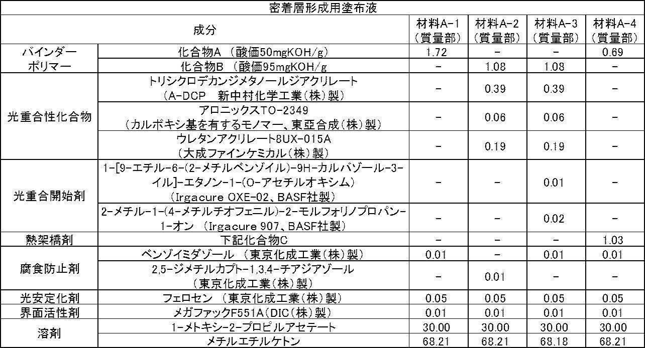
TO-2349:カルボキシ基を有するモノマー(東亞合成(株)製、アロニックス(登録商標)TO-2349、5官能エチレン性不飽和化合物と6官能エチレン性不飽和化合物との混合物)
化合物A:下記の構成単位を有する化合物

化合物B:下記の構成単位を有する化合物(Mw:20000)
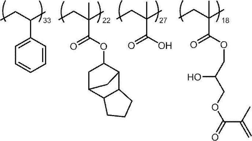
化合物C:下記の構成単位を有する化合物(Mw:5500)

<ネガ型感光性樹脂層形成用塗布液の調製>
下記表2の記載にしたがって、ネガ型感光性樹脂層形成用塗布液である材料BN-1を調製した。
下記表2の記載にしたがって、ネガ型感光性樹脂層形成用塗布液である材料BN-1を調製した。
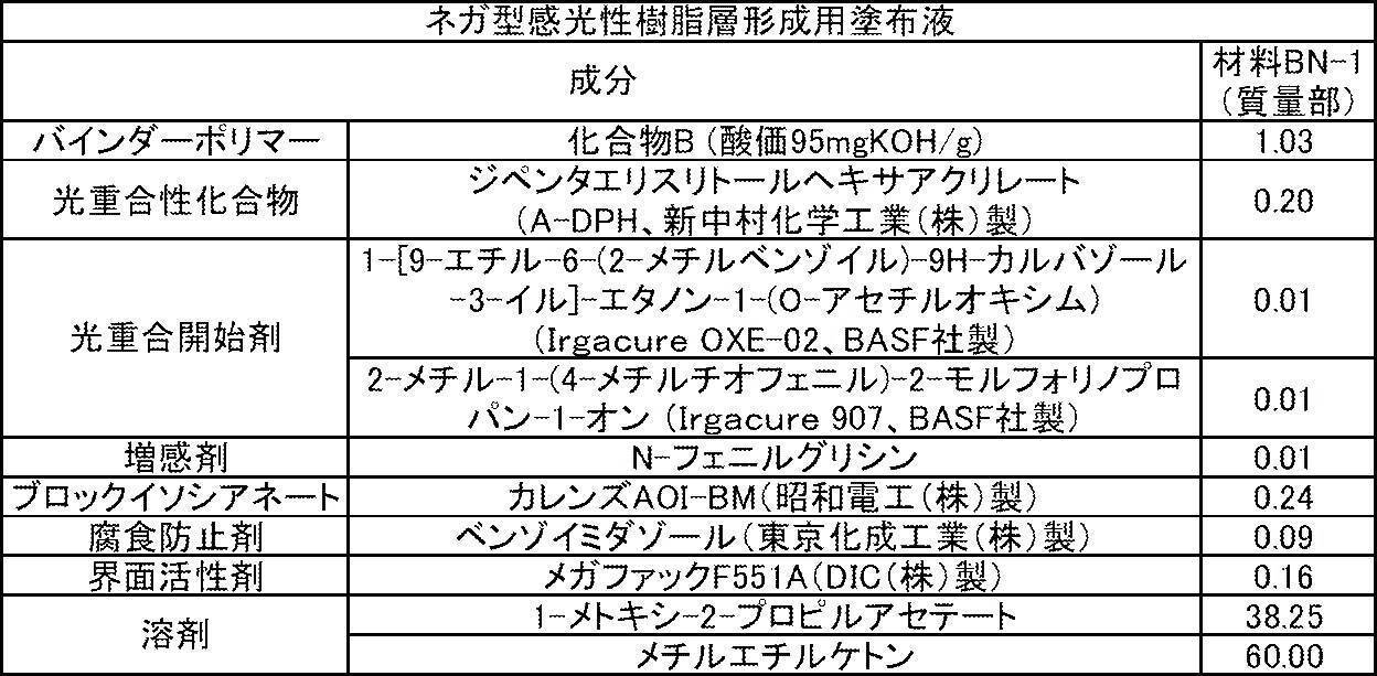
カレンズAOI-BM:アクリル酸2-(O-[1’-メチルプロピリデンアミノ]カルボニルアミノ)エチル、昭和電工(株)製
<ポジ型感光性樹脂層形成用塗布液の調製>
下記表3の記載にしたがって、ポジ型感光性樹脂層形成用塗布液である材料BP-1を調製した。後述する化合物Dにおいて各構成単位に併記された数値は、構成単位の含有比率(モル比)を表す。また、材料BP-1は、密着層形成用塗布液としても使用する。
下記表3の記載にしたがって、ポジ型感光性樹脂層形成用塗布液である材料BP-1を調製した。後述する化合物Dにおいて各構成単位に併記された数値は、構成単位の含有比率(モル比)を表す。また、材料BP-1は、密着層形成用塗布液としても使用する。

化合物D:下記の構成単位を有する化合物(Mw:25000)

化合物E:下記の構造を有する化合物
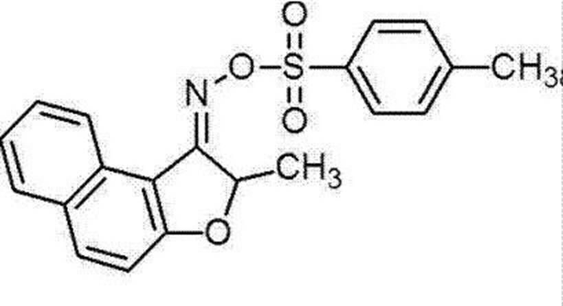
<第2の樹脂層形成用塗布液の調製>
下記表4の記載にしたがって、第2の樹脂層形成用塗布液である材料C-1を調製した。
下記表4の記載にしたがって、第2の樹脂層形成用塗布液である材料C-1を調製した。
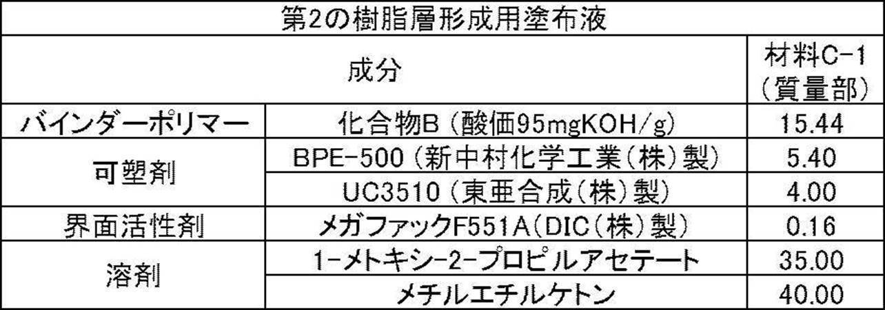
<中間層形成用塗布液の調製>
下記表5の記載にしたがって、中間層形成用塗布液である材料D-1を調製した。
下記表5の記載にしたがって、中間層形成用塗布液である材料D-1を調製した。

<実施例1~6、及び比較例1の導電性転写材料の作製>
厚さ16μmのポリエチレンテレフタレートフィルム(仮支持体、ルミラー16KS40(東レ株式会社製))の上に、スリット状ノズルを用いて、第2の樹脂層形成用塗布液である材料C-1を塗布した後、100℃で溶剤を乾燥させることで、第2の樹脂層を形成した。材料C-1の塗布量は、乾燥後の厚さが表6の記載の厚さとなる量に調整した。
上記第2の樹脂層上に、中間層形成用塗布液である材料D-1を塗布した後、100℃で乾燥することで、中間層を形成した。材料D-1の塗布量は、乾燥後の厚さが表6の記載の厚さとなる量に調整した。
上記中間層上に、ネガ型感光性樹脂層形成用塗布液である材料BN-1を塗布した後、100℃で乾燥することで、ネガ型感光性樹脂層(即ち、第1の樹脂層)を形成した。材料BN-1の塗布量は、乾燥後の厚さが表6の記載の厚さとなる量に調整した。
上記ネガ型感光性樹脂層上に、ウェット膜厚20μmで銀ナノワイヤー層形成用塗布液を塗布し、次いで、100℃の乾燥温度で乾燥させることで、銀ナノワイヤー層(即ち銀ナノワイヤーを含む層)を形成した。銀ナノワイヤー層の膜厚は100nmであった。
上記銀ナノワイヤー層の上に、下記表6の記載にしたがって選択した密着層形成用塗布液である材料A-1~A-4のいずれかを塗布した。材料A-1~A-4の塗布量は、乾燥後の厚さが表6に記載の厚さとなる量に調整した。材料A-1~A-4の塗布後、100℃の乾燥温度で乾燥させ、密着層を形成した。
次に、上記密着層の上に厚さ16μmのポリエチレンテレフタレートフィルム(保護フィルム、ルミラー16KS40(東レ株式会社製))を圧着し、実施例1~6、及び比較例1の導電性転写材料をそれぞれ作製した。
厚さ16μmのポリエチレンテレフタレートフィルム(仮支持体、ルミラー16KS40(東レ株式会社製))の上に、スリット状ノズルを用いて、第2の樹脂層形成用塗布液である材料C-1を塗布した後、100℃で溶剤を乾燥させることで、第2の樹脂層を形成した。材料C-1の塗布量は、乾燥後の厚さが表6の記載の厚さとなる量に調整した。
上記第2の樹脂層上に、中間層形成用塗布液である材料D-1を塗布した後、100℃で乾燥することで、中間層を形成した。材料D-1の塗布量は、乾燥後の厚さが表6の記載の厚さとなる量に調整した。
上記中間層上に、ネガ型感光性樹脂層形成用塗布液である材料BN-1を塗布した後、100℃で乾燥することで、ネガ型感光性樹脂層(即ち、第1の樹脂層)を形成した。材料BN-1の塗布量は、乾燥後の厚さが表6の記載の厚さとなる量に調整した。
上記ネガ型感光性樹脂層上に、ウェット膜厚20μmで銀ナノワイヤー層形成用塗布液を塗布し、次いで、100℃の乾燥温度で乾燥させることで、銀ナノワイヤー層(即ち銀ナノワイヤーを含む層)を形成した。銀ナノワイヤー層の膜厚は100nmであった。
上記銀ナノワイヤー層の上に、下記表6の記載にしたがって選択した密着層形成用塗布液である材料A-1~A-4のいずれかを塗布した。材料A-1~A-4の塗布量は、乾燥後の厚さが表6に記載の厚さとなる量に調整した。材料A-1~A-4の塗布後、100℃の乾燥温度で乾燥させ、密着層を形成した。
次に、上記密着層の上に厚さ16μmのポリエチレンテレフタレートフィルム(保護フィルム、ルミラー16KS40(東レ株式会社製))を圧着し、実施例1~6、及び比較例1の導電性転写材料をそれぞれ作製した。
<実施例7の導電性転写材料の作製>
厚さ16μmのポリエチレンテレフタレートフィルム(保護フィルム、ルミラー16KS40(東レ株式会社製))の上に、スリット状ノズルを用いて、密着層形成用塗布液である材料A-1を塗布し、密着層を形成した。材料A-1の塗布量は、乾燥後の厚さが表6に記載の厚さとなる量に調整した。
100℃で溶剤を揮発させた後、密着層上に、スリット状ノズルを用いて、WET塗布厚さ20μmで銀ナノワイヤー層形成用塗布液を塗布し、次いで、100℃の乾燥温度で乾燥させることで、銀ナノワイヤー層(即ち銀ナノワイヤーを含む層)を形成した。銀ナノワイヤー層の膜厚は100nmであった。
上記銀ナノワイヤー層の上に、ネガ型感光性樹脂層形成用塗布液である材料BN-1を塗布した後、100℃で乾燥することで、ネガ型の感光性樹脂層(即ち、第1の樹脂層)を形成した。材料BN-1の塗布量は、乾燥後の厚さが表6の記載の厚さとなる量に調整した。
厚さ16μmのポリエチレンテレフタレートフィルム(仮支持体、ルミラー16KS40(東レ株式会社製))上に、第2の樹脂層形成用塗布液である材料C-1を塗布した後、100℃で溶剤を乾燥させることで、第2の樹脂層を形成した。
以上の手順によって作製された、保護フィルム、密着層、銀ナノワイヤー層、及びネガ型の感光性樹脂層を有する第1の多層体と、仮支持体、及び第2の樹脂層を有する第2の多層体とを貼り合わせることで、仮支持体と、第2の樹脂層と、ネガ型の感光性樹脂層と、銀ナノワイヤー層と、密着層と、保護フィルムと、をこの順で有する実施例7の導電性転写材料を作製した。
厚さ16μmのポリエチレンテレフタレートフィルム(保護フィルム、ルミラー16KS40(東レ株式会社製))の上に、スリット状ノズルを用いて、密着層形成用塗布液である材料A-1を塗布し、密着層を形成した。材料A-1の塗布量は、乾燥後の厚さが表6に記載の厚さとなる量に調整した。
100℃で溶剤を揮発させた後、密着層上に、スリット状ノズルを用いて、WET塗布厚さ20μmで銀ナノワイヤー層形成用塗布液を塗布し、次いで、100℃の乾燥温度で乾燥させることで、銀ナノワイヤー層(即ち銀ナノワイヤーを含む層)を形成した。銀ナノワイヤー層の膜厚は100nmであった。
上記銀ナノワイヤー層の上に、ネガ型感光性樹脂層形成用塗布液である材料BN-1を塗布した後、100℃で乾燥することで、ネガ型の感光性樹脂層(即ち、第1の樹脂層)を形成した。材料BN-1の塗布量は、乾燥後の厚さが表6の記載の厚さとなる量に調整した。
厚さ16μmのポリエチレンテレフタレートフィルム(仮支持体、ルミラー16KS40(東レ株式会社製))上に、第2の樹脂層形成用塗布液である材料C-1を塗布した後、100℃で溶剤を乾燥させることで、第2の樹脂層を形成した。
以上の手順によって作製された、保護フィルム、密着層、銀ナノワイヤー層、及びネガ型の感光性樹脂層を有する第1の多層体と、仮支持体、及び第2の樹脂層を有する第2の多層体とを貼り合わせることで、仮支持体と、第2の樹脂層と、ネガ型の感光性樹脂層と、銀ナノワイヤー層と、密着層と、保護フィルムと、をこの順で有する実施例7の導電性転写材料を作製した。
<実施例8~10の導電性転写材料の作製>
第1の樹脂層の形成と密着層の形成とを下記のように変更した以外は実施例1と同様に作製した。
中間層上に、ポジ型感光性樹脂層形成用塗布液である材料BP-1を塗布した後、100℃で乾燥することで、ポジ型感光性樹脂層(即ち、第1の樹脂層)を形成した。材料BP-1の塗布量は、乾燥後の厚さが表6の記載の厚さとなる量に調整した。
銀ナノワイヤー層の上に、下記表6の記載にしたがって選択した密着層形成用塗布液である材料A-1、材料A-4及び材料BP-1のいずれかを塗布し、100℃の乾燥温度で乾燥させ、密着層を形成した。材料A-1、材料A-4及び材料BP-1の塗布量は、乾燥後の厚さが表6に記載の厚さとなる量に調整した。
第1の樹脂層の形成と密着層の形成とを下記のように変更した以外は実施例1と同様に作製した。
中間層上に、ポジ型感光性樹脂層形成用塗布液である材料BP-1を塗布した後、100℃で乾燥することで、ポジ型感光性樹脂層(即ち、第1の樹脂層)を形成した。材料BP-1の塗布量は、乾燥後の厚さが表6の記載の厚さとなる量に調整した。
銀ナノワイヤー層の上に、下記表6の記載にしたがって選択した密着層形成用塗布液である材料A-1、材料A-4及び材料BP-1のいずれかを塗布し、100℃の乾燥温度で乾燥させ、密着層を形成した。材料A-1、材料A-4及び材料BP-1の塗布量は、乾燥後の厚さが表6に記載の厚さとなる量に調整した。
<透明電極パターンフィルムの作製>
保護フィルムを剥離した実施例1~10及び比較例1の導電性転写材料を、厚さ38μm、屈折率1.53のシクロオレフィンポリマーフィルム上に貼り合わせること(以下、本段落において「ラミネート加工」という。)によって、パターン形成用積層体を得た。ラミネート加工は、MCK社製真空ラミネーターを用いて、シクロオレフィンポリマーフィルム温度40℃、ゴムローラー温度100℃、線圧3N/cm、搬送速度2m/分の条件で行った。また、ラミネート加工においては、導電性転写材料から保護フィルムを剥離することによって露出する面を、シクロオレフィンポリマーフィルム表面に接触させた。
超高圧水銀灯を有するプロキシミティー型露光機(日立ハイテク電子エンジニアリング(株)製)を用いて、露光マスク(透明電極形成用パターンを有す石英露光マスク)面と仮支持体とを密着させ、仮支持体を介して露光量100mJ/cm2(i線)で第1の樹脂層をパターン露光した。なお、実施例1~7と実施例8~10とでマスクをそれぞれネガ型感光性脂層用、ポジ型感光性樹脂層用と使い分けた。
仮支持体を剥離後、炭酸ソーダ1質量%水溶液を用いて、32℃で60秒間現像処理を実施した。現像処理後、透明電極パターンフィルムに超高圧洗浄ノズルから超純水を噴射することで残渣を除去した。これにより密着層、銀ナノワイヤー層、及び第1の樹脂層をパターニングした。その後、エアを吹きかけて透明電極パターンフィルム上の水分を除去した。
次いで、145℃、10分の加熱処理を行うことで、パターン化された銀ナノワイヤー層を有する透明電極パターンフィルム(パターンつき基板)を作製した。
保護フィルムを剥離した実施例1~10及び比較例1の導電性転写材料を、厚さ38μm、屈折率1.53のシクロオレフィンポリマーフィルム上に貼り合わせること(以下、本段落において「ラミネート加工」という。)によって、パターン形成用積層体を得た。ラミネート加工は、MCK社製真空ラミネーターを用いて、シクロオレフィンポリマーフィルム温度40℃、ゴムローラー温度100℃、線圧3N/cm、搬送速度2m/分の条件で行った。また、ラミネート加工においては、導電性転写材料から保護フィルムを剥離することによって露出する面を、シクロオレフィンポリマーフィルム表面に接触させた。
超高圧水銀灯を有するプロキシミティー型露光機(日立ハイテク電子エンジニアリング(株)製)を用いて、露光マスク(透明電極形成用パターンを有す石英露光マスク)面と仮支持体とを密着させ、仮支持体を介して露光量100mJ/cm2(i線)で第1の樹脂層をパターン露光した。なお、実施例1~7と実施例8~10とでマスクをそれぞれネガ型感光性脂層用、ポジ型感光性樹脂層用と使い分けた。
仮支持体を剥離後、炭酸ソーダ1質量%水溶液を用いて、32℃で60秒間現像処理を実施した。現像処理後、透明電極パターンフィルムに超高圧洗浄ノズルから超純水を噴射することで残渣を除去した。これにより密着層、銀ナノワイヤー層、及び第1の樹脂層をパターニングした。その後、エアを吹きかけて透明電極パターンフィルム上の水分を除去した。
次いで、145℃、10分の加熱処理を行うことで、パターン化された銀ナノワイヤー層を有する透明電極パターンフィルム(パターンつき基板)を作製した。
<評価>
[ヘイズ]
ヘイズメーターNDH4000(日本電色工業株式会社製)により、上記で作製した透明電極パターンフィルムのヘイズを測定した。評価結果を表6に示す。
[ヘイズ]
ヘイズメーターNDH4000(日本電色工業株式会社製)により、上記で作製した透明電極パターンフィルムのヘイズを測定した。評価結果を表6に示す。
[面状異常]
上記で作製した透明電極パターンフィルムの上に、リンテック株式会社製の光学粘着シートMO-series(厚さ50μm)を室温下で積層した。得られた試験体を、顕微鏡を用いて200倍の倍率で観察し、下記基準にしたがって面状異常を評価した。実用上、A又はBである必要があり、Aであることが好ましい。評価結果を表6に示す。
上記で作製した透明電極パターンフィルムの上に、リンテック株式会社製の光学粘着シートMO-series(厚さ50μm)を室温下で積層した。得られた試験体を、顕微鏡を用いて200倍の倍率で観察し、下記基準にしたがって面状異常を評価した。実用上、A又はBである必要があり、Aであることが好ましい。評価結果を表6に示す。
(基準)
A:全く異常が見られない。
B:パターンの段差に気泡が若干見られるが実用上問題ない。
C:明らかにパターンの段差に気泡が入っており、実用上問題となる。
A:全く異常が見られない。
B:パターンの段差に気泡が若干見られるが実用上問題ない。
C:明らかにパターンの段差に気泡が入っており、実用上問題となる。
[シート抵抗]
非接触式の渦電流方式の抵抗測定器EC-80P(ナプソン株式会社製)を用いて、上記で作製した透明電極パターンフィルムのシート抵抗を測定した。評価結果を表6に示す。
非接触式の渦電流方式の抵抗測定器EC-80P(ナプソン株式会社製)を用いて、上記で作製した透明電極パターンフィルムのシート抵抗を測定した。評価結果を表6に示す。

表6より、実施例1~10の導電性転写材料によれば、比較例1の導電性転写材料に比べて、パターンとパターン上に積層される層との密着界面における面状異常を低減できることがわかった。
2018年12月27日に出願された日本国特許出願2018-246222号の開示は、その全体が参照により本明細書に取り込まれる。本明細書に記載された全ての文献、特許出願、及び技術規格は、個々の文献、特許出願、及び技術規格が参照により取り込まれることが具体的かつ個々に記載された場合と同程度に、本明細書に参照により取り込まれる。
Claims (12)
- 仮支持体と、
厚さが1nm~300nmである第1の樹脂層と、
銀ナノワイヤーを含む層と、
をこの順で有する導電性転写材料。 - 前記銀ナノワイヤーを含む層の、前記第1の樹脂層とは反対側の面上に、厚さが1nm~250nmである密着層を有する請求項1に記載の導電性転写材料。
- 前記第1の樹脂層、前記銀ナノワイヤーを含む層、及び前記密着層からなる群より選択される少なくとも1つが、腐食防止剤を含有する請求項2に記載の導電性転写材料。
- 前記密着層が、アルカリ可溶性樹脂を含有する請求項2又は請求項3に記載の導電性転写材料。
- 前記仮支持体と前記第1の樹脂層との間に、第2の樹脂層を有する請求項1~請求項4のいずれか1項に記載の導電性転写材料。
- 前記第1の樹脂層が、感光性樹脂層である請求項1~請求項5のいずれか1項に記載の導電性転写材料。
- 前記感光性樹脂層が、ネガ型の感光性樹脂層である請求項6に記載の導電性転写材料。
- 請求項6又は請求項7に記載の導電性転写材料、及び基板を貼り合わせる工程と、
前記導電性転写材料における感光性樹脂層をパターン露光する工程と、
前記パターン露光を経た導電性転写材料を現像してパターンを形成する工程と、
をこの順に含む、パターンつき基板の製造方法。 - 基板と、
銀ナノワイヤーを含む層と、
厚さが1nm~300nmである第1の樹脂層と、
をこの順で有する積層体。 - 前記銀ナノワイヤーを含む層及び前記第1の樹脂層が、転写層である請求項9に記載の積層体。
- 前記基板と前記銀ナノワイヤーを含む層との間に、厚さが1nm~250nmである密着層を有する請求項9又は請求項10に記載の積層体。
- 請求項9~請求項11のいずれか1項に記載の積層体を有するタッチパネル。
Priority Applications (2)
| Application Number | Priority Date | Filing Date | Title |
|---|---|---|---|
| CN201980086087.XA CN113302555A (zh) | 2018-12-27 | 2019-12-19 | 导电性转印材料、附有图案的基板的制造方法、层叠体及触控面板 |
| JP2020563163A JPWO2020137797A1 (ja) | 2018-12-27 | 2019-12-19 | 導電性転写材料、パターンつき基板の製造方法、積層体、及びタッチパネル |
Applications Claiming Priority (2)
| Application Number | Priority Date | Filing Date | Title |
|---|---|---|---|
| JP2018246222 | 2018-12-27 | ||
| JP2018-246222 | 2018-12-27 |
Publications (1)
| Publication Number | Publication Date |
|---|---|
| WO2020137797A1 true WO2020137797A1 (ja) | 2020-07-02 |
Family
ID=71128656
Family Applications (1)
| Application Number | Title | Priority Date | Filing Date |
|---|---|---|---|
| PCT/JP2019/049814 Ceased WO2020137797A1 (ja) | 2018-12-27 | 2019-12-19 | 導電性転写材料、パターンつき基板の製造方法、積層体、及びタッチパネル |
Country Status (4)
| Country | Link |
|---|---|
| JP (1) | JPWO2020137797A1 (ja) |
| CN (1) | CN113302555A (ja) |
| TW (1) | TW202041969A (ja) |
| WO (1) | WO2020137797A1 (ja) |
Cited By (4)
| Publication number | Priority date | Publication date | Assignee | Title |
|---|---|---|---|---|
| JP2022032022A (ja) * | 2020-08-10 | 2022-02-24 | カンブリオス フィルム ソリューションズ(シアメン) コーポレーション | 透明導電膜及びその製造方法 |
| JPWO2022102675A1 (ja) * | 2020-11-13 | 2022-05-19 | ||
| JP2022110455A (ja) * | 2021-01-18 | 2022-07-29 | 太陽インキ製造株式会社 | 感光性積層樹脂構造体、ドライフィルム、硬化物および電子部品 |
| WO2023090253A1 (ja) * | 2021-11-22 | 2023-05-25 | 富士フイルム株式会社 | 積層体及びその製造方法、並びに電子デバイス |
Families Citing this family (1)
| Publication number | Priority date | Publication date | Assignee | Title |
|---|---|---|---|---|
| TWI775269B (zh) * | 2021-01-11 | 2022-08-21 | 大陸商天材創新材料科技(廈門)有限公司 | 疊構結構及觸控感應器 |
Citations (4)
| Publication number | Priority date | Publication date | Assignee | Title |
|---|---|---|---|---|
| JP2012033466A (ja) * | 2010-07-02 | 2012-02-16 | Fujifilm Corp | 導電層転写材料、及びタッチパネル |
| JP2016534465A (ja) * | 2013-08-28 | 2016-11-04 | スリーエム イノベイティブ プロパティズ カンパニー | 以降の処理工程中における、正確な位置合わせのための、基準マークを備える電子アセンブリ |
| JP2018128670A (ja) * | 2012-03-29 | 2018-08-16 | シーエーエム ホールディング コーポレーション | 表面を有するナノ構造層を含む構造を形成する方法 |
| US20180301543A1 (en) * | 2017-04-13 | 2018-10-18 | Tsinghua University | Method for making thin film transistor |
Family Cites Families (6)
| Publication number | Priority date | Publication date | Assignee | Title |
|---|---|---|---|---|
| TW201324546A (zh) * | 2011-09-26 | 2013-06-16 | Dainippon Ink & Chemicals | 附透明導電層之基體及其製造方法 |
| JP2013202911A (ja) * | 2012-03-28 | 2013-10-07 | Dic Corp | 透明導電層付き基体の製造方法 |
| JP2014191894A (ja) * | 2013-03-26 | 2014-10-06 | Dic Corp | 透明導電フィルム及びタッチパネル |
| JPWO2015068654A1 (ja) * | 2013-11-05 | 2017-03-09 | 昭和電工株式会社 | 導電パターン形成方法及びこれを使用したオンセル型タッチパネルの製造方法並びにこれに使用する転写用フィルム及びオンセル型タッチパネル |
| US20150255186A1 (en) * | 2014-03-06 | 2015-09-10 | Panasonic Intellectual Property Management Co., Ltd. | Base material with a transparent conductive film, method for manufacturing the same, touch panel, and solar cell |
| JP6502126B2 (ja) * | 2015-03-05 | 2019-04-17 | アルプスアルパイン株式会社 | 導電パターン形成用熱転写リボン及び導電パターンの形成方法 |
-
2019
- 2019-12-19 JP JP2020563163A patent/JPWO2020137797A1/ja not_active Abandoned
- 2019-12-19 WO PCT/JP2019/049814 patent/WO2020137797A1/ja not_active Ceased
- 2019-12-19 CN CN201980086087.XA patent/CN113302555A/zh active Pending
- 2019-12-25 TW TW108147666A patent/TW202041969A/zh unknown
Patent Citations (4)
| Publication number | Priority date | Publication date | Assignee | Title |
|---|---|---|---|---|
| JP2012033466A (ja) * | 2010-07-02 | 2012-02-16 | Fujifilm Corp | 導電層転写材料、及びタッチパネル |
| JP2018128670A (ja) * | 2012-03-29 | 2018-08-16 | シーエーエム ホールディング コーポレーション | 表面を有するナノ構造層を含む構造を形成する方法 |
| JP2016534465A (ja) * | 2013-08-28 | 2016-11-04 | スリーエム イノベイティブ プロパティズ カンパニー | 以降の処理工程中における、正確な位置合わせのための、基準マークを備える電子アセンブリ |
| US20180301543A1 (en) * | 2017-04-13 | 2018-10-18 | Tsinghua University | Method for making thin film transistor |
Cited By (5)
| Publication number | Priority date | Publication date | Assignee | Title |
|---|---|---|---|---|
| JP2022032022A (ja) * | 2020-08-10 | 2022-02-24 | カンブリオス フィルム ソリューションズ(シアメン) コーポレーション | 透明導電膜及びその製造方法 |
| JPWO2022102675A1 (ja) * | 2020-11-13 | 2022-05-19 | ||
| JP2022110455A (ja) * | 2021-01-18 | 2022-07-29 | 太陽インキ製造株式会社 | 感光性積層樹脂構造体、ドライフィルム、硬化物および電子部品 |
| JP7780869B2 (ja) | 2021-01-18 | 2025-12-05 | 太陽ホールディングス株式会社 | 感光性積層樹脂構造体、ドライフィルム、硬化物および電子部品 |
| WO2023090253A1 (ja) * | 2021-11-22 | 2023-05-25 | 富士フイルム株式会社 | 積層体及びその製造方法、並びに電子デバイス |
Also Published As
| Publication number | Publication date |
|---|---|
| CN113302555A (zh) | 2021-08-24 |
| TW202041969A (zh) | 2020-11-16 |
| JPWO2020137797A1 (ja) | 2021-11-11 |
Similar Documents
| Publication | Publication Date | Title |
|---|---|---|
| WO2020137797A1 (ja) | 導電性転写材料、パターンつき基板の製造方法、積層体、及びタッチパネル | |
| JP6858269B2 (ja) | 回路配線の製造方法、タッチパネルの製造方法及びパターン付き基材の製造方法 | |
| JP6591078B2 (ja) | 感光性樹脂組成物、転写フィルム、タッチパネル用保護膜、タッチパネル及びその製造方法、並びに画像表示装置 | |
| JP6683890B2 (ja) | 感光性転写材料、及び、回路配線の製造方法 | |
| JP6999693B2 (ja) | 感光性転写材料、樹脂パターン製造方法、及び、配線製造方法 | |
| JP2019191518A (ja) | 感光性転写材料、レジストパターンの製造方法、回路配線の製造方法 | |
| KR20190003641A (ko) | 패턴이 형성된 기재의 제조 방법, 및 회로 기판의 제조 방법 | |
| WO2020137284A1 (ja) | 導電性転写材料、パターンつき基板の製造方法、回路基板の製造方法、積層体、及びタッチパネル | |
| JP6968273B2 (ja) | 感光性転写材料、樹脂パターンの製造方法、回路配線の製造方法、及び、タッチパネルの製造方法 | |
| JP7317102B2 (ja) | 導電性転写材料及び導電パターンの製造方法 | |
| JP2016177556A (ja) | タッチパネル部材、タッチパネル及びタッチパネル表示装置 | |
| TW201922817A (zh) | 電路配線的製造方法及觸控面板的製造方法 | |
| CN112166377A (zh) | 感光性转印材料、树脂图案的制造方法、电路布线的制造方法及触摸面板的制造方法 | |
| JP2019204070A (ja) | 感光性転写材料、回路配線の製造方法、及び、タッチパネルの製造方法 | |
| WO2020116068A1 (ja) | 転写材料、樹脂パターンの製造方法、回路配線の製造方法、及びタッチパネルの製造方法 | |
| WO2020174767A1 (ja) | パターンつき基板の製造方法、回路基板の製造方法、タッチパネルの製造方法、及び積層体 | |
| WO2020137144A1 (ja) | 感光性転写材料、積層体、タッチパネル、パターン付き基板の製造方法、回路基板の製造方法、及びタッチパネルの製造方法 | |
| JP7152593B2 (ja) | 転写フィルム、及び、パターン付き基板の製造方法 | |
| JP2018177889A (ja) | 感光性転写材料用重合体溶液の製造方法、感光性転写材料用組成物の製造方法、感光性転写材料の製造方法、回路配線の製造方法、及び、タッチパネルの製造方法 | |
| WO2023090253A1 (ja) | 積層体及びその製造方法、並びに電子デバイス | |
| WO2021024650A1 (ja) | 感光性転写部材、樹脂パターンの製造方法、回路配線の製造方法、タッチパネルの製造方法 | |
| WO2019225460A1 (ja) | 感光性転写材料、回路配線の製造方法、及びタッチパネルの製造方法 |
Legal Events
| Date | Code | Title | Description |
|---|---|---|---|
| 121 | Ep: the epo has been informed by wipo that ep was designated in this application |
Ref document number: 19902611 Country of ref document: EP Kind code of ref document: A1 |
|
| ENP | Entry into the national phase |
Ref document number: 2020563163 Country of ref document: JP Kind code of ref document: A |
|
| NENP | Non-entry into the national phase |
Ref country code: DE |
|
| 122 | Ep: pct application non-entry in european phase |
Ref document number: 19902611 Country of ref document: EP Kind code of ref document: A1 |