WO2020137289A1 - 導電性ペースト、電子部品、及び積層セラミックコンデンサ - Google Patents
導電性ペースト、電子部品、及び積層セラミックコンデンサ Download PDFInfo
- Publication number
- WO2020137289A1 WO2020137289A1 PCT/JP2019/045824 JP2019045824W WO2020137289A1 WO 2020137289 A1 WO2020137289 A1 WO 2020137289A1 JP 2019045824 W JP2019045824 W JP 2019045824W WO 2020137289 A1 WO2020137289 A1 WO 2020137289A1
- Authority
- WO
- WIPO (PCT)
- Prior art keywords
- conductive paste
- dispersant
- mass
- acid
- less
- Prior art date
- Legal status (The legal status is an assumption and is not a legal conclusion. Google has not performed a legal analysis and makes no representation as to the accuracy of the status listed.)
- Ceased
Links
Images

Classifications
-
- H—ELECTRICITY
- H01—ELECTRIC ELEMENTS
- H01B—CABLES; CONDUCTORS; INSULATORS; SELECTION OF MATERIALS FOR THEIR CONDUCTIVE, INSULATING OR DIELECTRIC PROPERTIES
- H01B1/00—Conductors or conductive bodies characterised by the conductive materials; Selection of materials as conductors
- H01B1/20—Conductive material dispersed in non-conductive organic material
- H01B1/22—Conductive material dispersed in non-conductive organic material the conductive material comprising metals or alloys
-
- C—CHEMISTRY; METALLURGY
- C08—ORGANIC MACROMOLECULAR COMPOUNDS; THEIR PREPARATION OR CHEMICAL WORKING-UP; COMPOSITIONS BASED THEREON
- C08K—Use of inorganic or non-macromolecular organic substances as compounding ingredients
- C08K3/00—Use of inorganic substances as compounding ingredients
- C08K3/02—Elements
- C08K3/08—Metals
-
- C—CHEMISTRY; METALLURGY
- C08—ORGANIC MACROMOLECULAR COMPOUNDS; THEIR PREPARATION OR CHEMICAL WORKING-UP; COMPOSITIONS BASED THEREON
- C08K—Use of inorganic or non-macromolecular organic substances as compounding ingredients
- C08K3/00—Use of inorganic substances as compounding ingredients
- C08K3/18—Oxygen-containing compounds, e.g. metal carbonyls
- C08K3/24—Acids; Salts thereof
-
- C—CHEMISTRY; METALLURGY
- C08—ORGANIC MACROMOLECULAR COMPOUNDS; THEIR PREPARATION OR CHEMICAL WORKING-UP; COMPOSITIONS BASED THEREON
- C08K—Use of inorganic or non-macromolecular organic substances as compounding ingredients
- C08K5/00—Use of organic ingredients
- C08K5/04—Oxygen-containing compounds
- C08K5/09—Carboxylic acids; Metal salts thereof; Anhydrides thereof
-
- C—CHEMISTRY; METALLURGY
- C08—ORGANIC MACROMOLECULAR COMPOUNDS; THEIR PREPARATION OR CHEMICAL WORKING-UP; COMPOSITIONS BASED THEREON
- C08K—Use of inorganic or non-macromolecular organic substances as compounding ingredients
- C08K5/00—Use of organic ingredients
- C08K5/16—Nitrogen-containing compounds
- C08K5/22—Compounds containing nitrogen bound to another nitrogen atom
-
- C—CHEMISTRY; METALLURGY
- C08—ORGANIC MACROMOLECULAR COMPOUNDS; THEIR PREPARATION OR CHEMICAL WORKING-UP; COMPOSITIONS BASED THEREON
- C08L—COMPOSITIONS OF MACROMOLECULAR COMPOUNDS
- C08L101/00—Compositions of unspecified macromolecular compounds
- C08L101/02—Compositions of unspecified macromolecular compounds characterised by the presence of specified groups, e.g. terminal or pendant functional groups
- C08L101/06—Compositions of unspecified macromolecular compounds characterised by the presence of specified groups, e.g. terminal or pendant functional groups containing oxygen atoms
- C08L101/08—Carboxyl groups
-
- C—CHEMISTRY; METALLURGY
- C08—ORGANIC MACROMOLECULAR COMPOUNDS; THEIR PREPARATION OR CHEMICAL WORKING-UP; COMPOSITIONS BASED THEREON
- C08L—COMPOSITIONS OF MACROMOLECULAR COMPOUNDS
- C08L29/00—Compositions of homopolymers or copolymers of compounds having one or more unsaturated aliphatic radicals, each having only one carbon-to-carbon double bond, and at least one being terminated by an alcohol, ether, aldehydo, ketonic, acetal or ketal radical; Compositions of hydrolysed polymers of esters of unsaturated alcohols with saturated carboxylic acids; Compositions of derivatives of such polymers
- C08L29/14—Homopolymers or copolymers of acetals or ketals obtained by polymerisation of unsaturated acetals or ketals or by after-treatment of polymers of unsaturated alcohols
-
- H—ELECTRICITY
- H01—ELECTRIC ELEMENTS
- H01G—CAPACITORS; CAPACITORS, RECTIFIERS, DETECTORS, SWITCHING DEVICES, LIGHT-SENSITIVE OR TEMPERATURE-SENSITIVE DEVICES OF THE ELECTROLYTIC TYPE
- H01G4/00—Fixed capacitors; Processes of their manufacture
- H01G4/002—Details
- H01G4/018—Dielectrics
- H01G4/06—Solid dielectrics
- H01G4/08—Inorganic dielectrics
- H01G4/12—Ceramic dielectrics
- H01G4/1209—Ceramic dielectrics characterised by the ceramic dielectric material
-
- H—ELECTRICITY
- H01—ELECTRIC ELEMENTS
- H01G—CAPACITORS; CAPACITORS, RECTIFIERS, DETECTORS, SWITCHING DEVICES, LIGHT-SENSITIVE OR TEMPERATURE-SENSITIVE DEVICES OF THE ELECTROLYTIC TYPE
- H01G4/00—Fixed capacitors; Processes of their manufacture
- H01G4/30—Stacked capacitors
Definitions
- the present invention relates to a conductive paste, an electronic component, and a monolithic ceramic capacitor.
- a monolithic ceramic capacitor has a structure in which a plurality of dielectric layers and a plurality of internal electrode layers are alternately laminated. By thinning these dielectric layers and internal electrode layers, downsizing and high capacity can be achieved. Can be planned.
- the monolithic ceramic capacitor is manufactured, for example, as follows. First, a conductive paste for internal electrodes is printed (applied) in a predetermined electrode pattern on the surface of a dielectric green sheet containing a dielectric powder such as barium titanate (BaTiO 3 ) and a binder resin, and dried. To form a dry film. Next, the dry films and the dielectric green sheets are laminated so as to be alternately superposed, and heat-pressed to be integrated to form a pressure-bonded body. This pressure-bonded body is cut, and after the organic binder treatment is performed in an oxidizing atmosphere or an inert atmosphere, firing is performed to obtain a fired chip (laminated body). Next, the external electrode paste is applied to both ends of the fired chip (multilayer body), and after firing, nickel plating or the like is applied to the surfaces of the external electrodes to obtain a multilayer ceramic capacitor.
- a conductive paste for internal electrodes is printed (applied) in a predetermined electrode pattern on the surface of a dielectric green
- a screen printing method As a printing method used when printing a conductive paste on a dielectric green sheet, a screen printing method has been generally used in the past, but due to demands for downsizing of electronic devices, thinning, and improvement in productivity. It is required to print finer electrode patterns with high productivity.
- a gravure is a continuous printing method in which the conductive paste is filled in the recesses provided in the plate making and the conductive paste is transferred from the plate making by pressing it against the surface to be printed.
- Printing methods have been proposed.
- the gravure printing method has high printing speed and excellent productivity.
- a conductive paste used for forming the internal conductor film in a multilayer ceramic electronic component including a plurality of ceramic layers and an internal conductor film extending along a specific interface between the ceramic layers by gravure printing.
- the viscosity ⁇ 0.1 at a shear rate of 0.1 (s ⁇ 1 ) is 1 Pa ⁇ s or more, and the viscosity at a shear rate of 0.02 (s ⁇ 1 ).
- a conductive paste, which is a thixotropic fluid, in which ⁇ 0.02 satisfies the condition represented by a specific formula is described.
- a conductive paste used for forming by gravure printing as in Patent Document 1 is used.
- the conductive paste contains metal powder in an amount of 30 to 70% by weight and a conductive component in an amount of 1 to 10% by weight.
- a thixotropic fluid containing a resin component, 0.05 to 5% by weight of a dispersant, and a balance of a solvent component, and having a viscosity at a shear rate of 0.1 (s ⁇ 1 ) of 1 Pa ⁇ s or more,
- a conductive paste is described in which the viscosity change rate at a shear rate of 10 (s -1 ) is 50% or more based on the viscosity at a shear rate of 0.1 (s -1 ).
- these conductive pastes are thixotropic fluids having a viscosity of 1 Pa ⁇ s or more at a shear rate of 0.1 (s ⁇ 1 ) and are stable at high speed in gravure printing. It is said that continuous printability can be obtained and a monolithic ceramic electronic component such as a monolithic ceramic capacitor can be manufactured with good production efficiency.
- an organic paste (B) the degree of polymerization is 10,000 to 50,000 or less polyvinyl butyral and the weight average molecular weight is 10,000 to 100,000 ethyl cellulose, and the organic solvent (C) is propylene glycol monobutyl ether.
- conductive paste for gravure printing which comprises a composition containing a polycarboxylic acid polymer or a salt of polycarboxylic acid as an inhibitor, is described. According to Patent Document 3, this conductive paste has a viscosity suitable for gravure printing, improves uniformity and stability of the paste, and has good dryness.
- conductive powder tends to have a smaller particle size.
- the particle size of the conductive powder is small, the specific surface area of the particle surface becomes large, so the surface activity of the conductive powder (metal powder) becomes high, and the dispersibility of the conductive paste may decrease, which is higher.
- a conductive paste having dispersibility There is a demand for a conductive paste having dispersibility.
- the conductive paste when the conductive paste is printed by using the gravure printing method, a paste viscosity lower than that of the screen printing method is required, so that the conductive powder having a relatively large specific gravity settles and the dispersibility of the paste is reduced. It is possible.
- the dispersibility of the paste is improved by removing the lumps in the conductive paste using a filter, but the lumps are removed. Since the manufacturing process is required, the manufacturing process tends to be complicated.
- an object of the present invention is to provide a conductive paste having excellent paste dispersibility and productivity and having a paste viscosity suitable for gravure printing.
- a first aspect of the present invention is a conductive paste containing a conductive powder, a ceramic powder, a dispersant, a binder resin and an organic solvent, wherein the dispersant is a first acid dispersant and a second acid dispersant.
- the first acid-based dispersant includes a dispersant, has an average molecular weight of more than 500 and 2,000 or less, and has at least one branched chain composed of a hydrocarbon group with respect to the main chain.
- a conductive paste in which the system dispersant has a carboxyl group other than the first acid dispersant, the binder resin contains an acetal resin, and the organic solvent contains a glycol ether solvent.
- the first acid dispersant is preferably an acid dispersant having a carboxyl group, and more preferably a hydrocarbon graft copolymer having a polycarboxylic acid as a main chain.
- the second acid dispersant preferably has a molecular weight of 5000 or less and contains an alkyl group having 10 to 20 carbon atoms or an alkenyl group having 10 to 20 carbon atoms.
- the first acid dispersant is contained in an amount of 0.2 parts by mass or more and 2 parts by mass or less based on 100 parts by mass of the conductive powder, and the second acid dispersant is 100 parts by mass of the conductive powder. On the other hand, it is preferably contained in an amount of 0.01 part by mass or more and 2 parts by mass or less.
- the conductive powder preferably contains at least one metal powder selected from Ni, Pd, Pt, Au, Ag, Cu and alloys thereof. Further, the conductive powder preferably has an average particle size of 0.05 ⁇ m or more and 1.0 ⁇ m or less. Further, the ceramic powder preferably contains a perovskite type oxide. Further, the ceramic powder preferably has an average particle diameter of 0.01 ⁇ m or more and 0.5 ⁇ m or less. Further, the binder resin preferably contains a butyral resin. Further, it is preferable that the conductive paste is for an internal electrode of a laminated ceramic component.
- the conductive paste has a viscosity of 0.8 Pa ⁇ S or less at a shear rate of 100 sec ⁇ 1 and a viscosity of 0.18 Pa ⁇ S or less at a shear rate of 10,000 sec ⁇ 1 .
- an electronic component formed using the above conductive paste is provided.
- a laminated ceramic capacitor having at least a laminated body in which a dielectric layer and an internal electrode layer are laminated, and the internal electrode layer is formed by using the above conductive paste.
- the conductive paste of the present invention has excellent paste dispersibility and productivity. Further, the conductive paste of the present invention has a viscosity suitable for gravure printing. In addition, the electrode pattern of an electronic component such as a laminated ceramic capacitor formed by using the conductive paste of the present invention has excellent printability of the conductive paste even when forming a thinned electrode, and has a uniform thickness.
- FIG. 1A is a perspective view showing a monolithic ceramic capacitor according to an embodiment
- FIG. 1B is a sectional view thereof.
- the conductive paste of this embodiment contains conductive powder, ceramic powder, a dispersant, a binder resin, and an organic solvent.
- conductive powder conductive powder, ceramic powder, a dispersant, a binder resin, and an organic solvent.
- the conductive powder is not particularly limited, and metal powder can be used, and for example, one or more kinds of powder selected from Ni, Pd, Pt, Au, Ag, Cu, and alloys thereof can be used. Among these, from the viewpoint of conductivity, corrosion resistance, and cost, it is preferable to use Ni or its alloy powder (hereinafter sometimes referred to as “Ni powder”).
- Ni powder Ni or its alloy powder
- the Ni alloy for example, an alloy of Ni and at least one element selected from the group consisting of Mn, Cr, Co, Al, Fe, Cu, Zn, Ag, Au, Pt and Pd may be used. it can.
- the Ni content in the Ni alloy is, for example, 50 mass% or more, preferably 80 mass% or more.
- the Ni powder may contain about several hundred ppm of the element S in order to suppress rapid gas generation due to partial thermal decomposition of the binder resin during the debinding process.
- the average particle size of the conductive powder is preferably 0.05 ⁇ m or more and 1.0 ⁇ m or less, more preferably 0.1 ⁇ m or more and 0.5 ⁇ m or less.
- the average particle size of the conductive powder is within the above range, it can be suitably used as a paste for internal electrodes of a thinned multilayer ceramic capacitor (multilayer ceramic component).
- the smoothness of the dry film and the dry film density are improves.
- the average particle size is a value obtained by observation with a scanning electron microscope (SEM), and is obtained by measuring the particle size of each of a plurality of particles from an image observed with a SEM at a magnification of 10,000 times. It is the average value of the number.
- the content of the conductive powder is preferably 30% by mass or more and less than 70% by mass, more preferably 40% by mass or more and 60% by mass or less, based on the total amount of the conductive paste.
- the conductivity and dispersibility are excellent.
- the ceramic powder is not particularly limited, and for example, in the case of a conductive paste for internal electrodes of a laminated ceramic capacitor, a known ceramic powder is appropriately selected according to the type of the laminated ceramic capacitor to be applied.
- the ceramic powder include a perovskite type oxide containing Ba and Ti, and preferably barium titanate (BaTiO 3 ).
- a ceramic powder containing barium titanate as a main component and an oxide as an auxiliary component may be used.
- the oxide include one or more kinds of oxides selected from Mn, Cr, Si, Ca, Ba, Mg, V, W, Ta, Nb and rare earth elements.
- the ceramic powder for example, a ceramic powder of a perovskite-type oxide ferroelectric in which Ba atom or Ti atom of barium titanate (BaTiO 3 ) is replaced with another atom, for example, Sn, Pb, Zr or the like is used. May be.
- the ceramic powder When used as a conductive paste for internal electrodes, the ceramic powder may have the same composition as the dielectric ceramic powder forming the dielectric green sheet of the laminated ceramic capacitor (electronic component). This suppresses the occurrence of cracks due to shrinkage mismatch at the interface between the dielectric layer and the internal electrode layer in the sintering process.
- a ceramic powder include ZnO, ferrite, PZT, BaO, Al 2 O 3 , Bi 2 O 3 , and R (rare earth element) 2 O 3 in addition to the above-described perovskite-type oxide containing Ba and Ti. , TiO 2 , Nd 2 O 3 and other oxides.
- the ceramic powder may be used alone or in combination of two or more.
- the average particle size of the ceramic powder is, for example, 0.01 ⁇ m or more and 0.5 ⁇ m or less, and preferably 0.01 ⁇ m or more and 0.3 ⁇ m or less.
- the average particle size is a value obtained by observation with a scanning electron microscope (SEM), and is obtained by measuring the particle size of each of a plurality of particles from an image observed with an SEM at a magnification of 50,000. It is the average value of the number.
- SEM scanning electron microscope
- the content of the ceramic powder is preferably 1 part by mass or more and 30 parts by mass or less, and more preferably 3 parts by mass or more and 30 parts by mass or less with respect to 100 parts by mass of the conductive powder.
- the content of the ceramic powder is preferably 1% by mass or more and 20% by mass or less, more preferably 3% by mass or more and 20% by mass or less, based on the total amount of the conductive paste.
- the binder resin contains an acetal resin.
- acetal resin butyral resin such as polyvinyl butyral is preferable.
- the binder resin may contain, for example, 20% by mass or more, 30% by mass or more of the acetal-based resin based on the entire binder resin, or may be composed of only the acetal-based resin. Further, even if the content of the acetal resin is less than 40% by mass with respect to the entire binder resin, it is possible to have a low paste viscosity and a sufficient adhesive strength.
- the content of the acetal resin is preferably 1 part by mass or more and 10 parts by mass or less, and more preferably 1 part by mass or more and 8 parts by mass or less with respect to 100 parts by mass of the conductive powder.
- the binder resin may include other resins below the acetal resin.
- the other resin is not particularly limited, and a known resin can be used.
- the other resin include, for example, methyl cellulose, ethyl cellulose, ethyl hydroxyethyl cellulose, cellulose resins such as nitrocellulose, acrylic resins, and the like. Among them, from the viewpoint of solubility in solvents, combustion decomposability, etc., ethyl cellulose is used. preferable.
- the molecular weight of the binder resin is, for example, about 20,000 to 200,000.
- the content of the binder resin is preferably 1 part by mass or more and 10 parts by mass or less, more preferably 1 part by mass or more and 8 parts by mass or less with respect to 100 parts by mass of the conductive powder.
- the content of the binder resin is preferably 0.5% by mass or more and 10% by mass or less, more preferably 0.5% by mass or more and 6% by mass or less, based on the total amount of the conductive paste.
- the conductivity and dispersibility are excellent.
- Organic solvent includes a glycol ether solvent.
- glycol ether solvent examples include (di)ethylene glycol ethers such as diethylene glycol mono-2-ethylhexyl ether, ethylene glycol mono-2-ethylhexyl ether, diethylene glycol monohexyl ether, ethylene glycol monohexyl ether, and propylene glycol.
- examples thereof include propylene glycol monoalkyl ethers such as monomethyl ether, propylene glycol monoethyl ether, propylene glycol monopropyl ether, and propylene glycol monobutyl ether (PNB).
- propylene glycol monoalkyl ethers are preferable, and propylene glycol monobutyl ether (PNB) is more preferable.
- the organic solvent contains a glycol ether-based solvent, it has excellent compatibility with the above-mentioned binder resin and excellent drying property.
- the organic solvent may include, for example, a glycol ether solvent in an amount of 25% by mass or more, or 50% by mass or more, or may be composed of only the glycol ether solvent, based on the entire organic solvent.
- the glycol ether solvent may be used alone or in combination of two or more.
- the organic solvent may further include an acetate solvent.
- the acetate solvent include dihydroterpinyl acetate, isobornyl acetate, isobornyl propionate, isobornyl butyrate, isobornyl isobutyrate, ethylene glycol monobutyl ether acetate and dipropylene glycol methyl ether.
- glycol ether acetates such as acetate, 3-methoxy-3-methylbutyl acetate and 1-methoxypropyl-2-acetate.
- the organic solvent includes an acetate solvent, for example, at least one acetate solvent selected from dihydroterpinyl acetate, isobornyl acetate, isobornyl propionate, isobornyl butyrate and isobornyl isobutyrate.
- the solvent (A) may be included. Among these, isobornyl acetate is more preferable.
- the acetate solvent is contained in the organic solvent in an amount of 0% by mass or more and 80% by mass or less, preferably 10% by mass or more and 60% by mass or less, and more preferably 20% by mass or more and 40% by mass or less. ..
- the organic solvent contains an acetate solvent
- the above-mentioned acetate solvent (A) and at least one acetate solvent (B) selected from ethylene glycol monobutyl ether acetate and dipropylene glycol methyl ether acetate. May be included.
- the viscosity of the conductive paste can be easily adjusted, and the drying speed of the conductive paste can be increased.
- the organic solvent is preferably 50% by mass or more and 90% by mass or less of the acetate solvent (A) with respect to the entire acetate solvent. It is contained, and more preferably 60 mass% or more and 80 mass% or less.
- the acetate solvent (B) is preferably contained in an amount of 10% by mass or more and 50% by mass or less, and more preferably 20% by mass or more and 40% by mass or less, based on 100% by mass of the whole acetate solvent. ..
- the organic solvent may include other organic solvent other than the glycol ether solvent and the acetate solvent.
- the other organic solvent is not particularly limited, and a known organic solvent capable of dissolving the binder resin can be used.
- organic solvents for example, ethyl acetate, propyl acetate, isobutyl acetate, acetic ester solvents such as butyl acetate, methyl ethyl ketone, ketone solvents such as methyl isobutyl ketone, terpineol, terpene solvents such as dihydroterpineol, tridecane
- Examples include aliphatic hydrocarbon solvents such as nonane and cyclohexane. Among them, the aliphatic hydrocarbon solvent is preferable, and mineral spirit is more preferable among the aliphatic hydrocarbon solvents.
- 1 type may be used for another organic solvent and 2 or more types may be used for it.
- the organic solvent may include, for example, a glycol ether solvent as the main solvent and an aliphatic hydrocarbon solvent as the auxiliary solvent.
- the glycol ether solvent is preferably contained in an amount of 30 parts by mass or more and 50 parts by mass or less, more preferably 40 parts by mass or more and 50 parts by mass or less, and 100 parts by mass of the conductive powder. Is preferably 20 parts by mass or more and 80 parts by mass or less, more preferably 20 parts by mass or more and 40 parts by mass or less with respect to 100 parts by mass of the conductive powder.
- the aliphatic hydrocarbon solvent is contained in an amount of 25 parts by mass or more based on 100 parts by mass of the conductive powder, the conductive paste can have excellent dispersibility.
- the content of the organic solvent is preferably 50 parts by mass or more and 130 parts by mass or less, more preferably 60 parts by mass or more and 90 parts by mass or less with respect to 100 parts by mass of the conductive powder.
- the conductivity and dispersibility are excellent.
- the content of the organic solvent is preferably 20% by mass or more and 50% by mass or less, and more preferably 25% by mass or more and 45% by mass or less, based on the total amount of the conductive paste.
- the conductivity and dispersibility are excellent.
- the present inventors As a result of studying various dispersants for the dispersant used in the conductive paste, the present inventors have found that the average molecular weight is more than 500 and not more than 2000, and a branched chain composed of a hydrocarbon group is added to the main chain. By using a dispersant containing a first acid dispersant having one or more and a second acid dispersant having a carboxyl group other than the first acid dispersant, it is contained in the conductive paste. It was found that the powder material (conductive powder or ceramic powder) has excellent dispersibility and the dry film surface has excellent smoothness.
- the first acid dispersant has a branch consisting of a hydrocarbon group, steric hindrance is effectively formed and aggregation of the powder material is suppressed.
- the second acid dispersant has a carboxyl group, it is considered that the carboxyl group can more effectively disperse the first acid dispersant.
- the molecular weight of the first acid-based dispersant is not bound by the above theory (reason).
- the dispersant according to this embodiment will be described in more detail.
- the first acid dispersant has at least one branched chain composed of a hydrocarbon group in the main chain, and preferably has a plurality of branched chains.
- the first acid dispersant preferably has a carboxyl group, and more preferably a hydrocarbon graft copolymer having a polycarboxylic acid as a main chain.
- the polycarboxylic acid preferably has an ester structure.
- the hydrocarbon group preferably has a chain structure.
- the hydrocarbon group may be an alkyl group.
- the alkyl group may be composed of only carbon and hydrogen, or a part of hydrogen constituting the alkyl group may be replaced with a substituent.
- the molecular weight of the first acid dispersant is greater than 500 and 2000 or less, and may be 1000 or more and 2000 or less. When the molecular weight is in the above range, the dispersibility of the conductive powder or the ceramic powder is excellent, and the density and smoothness of the dry film surface are excellent. In the present specification, when the molecular weight of the dispersant has a certain degree of distribution, the molecular weight of the dispersant indicates the weight average molecular weight.
- the first acid-based dispersant for example, a commercially available product that satisfies the above characteristics can be selected and used. Further, the acid-based dispersant may be manufactured so as to satisfy the above properties by using a conventionally known manufacturing method.
- the first acid dispersant is preferably contained in an amount of 0.2 parts by mass or more and 2 parts by mass or less based on 100 parts by mass of the conductive powder.
- the content of the acid-based dispersant is in the above range, the dispersibility of the conductive powder or the ceramic powder and the smoothness of the dried electrode surface after coating are excellent, and the viscosity of the conductive paste is adjusted to an appropriate range. It is also possible to suppress sheet attack and defective peeling of the green sheet. Further, the conductive paste according to the present embodiment can have high dispersibility even when the content of the acid-based dispersant is 1 part by mass or less.
- the second acid dispersant is an acid dispersant having a carboxyl group.
- the second acid dispersant preferably has a molecular weight of 5000 or less, more preferably 1000 or less, still more preferably 500 or less.
- the second acid dispersant is, for example, an acid dispersant having a hydrocarbon group.
- the hydrocarbon group preferably contains an alkyl group having 10 to 20 carbon atoms or an alkenyl group having 10 to 20 carbon atoms.
- Examples of the second acid dispersant include acid dispersants such as higher fatty acids and amino acids.
- the second dispersant may be used alone or in combination of two or more.
- the higher fatty acid may be an unsaturated carboxylic acid or a saturated carboxylic acid, and is not particularly limited, but carbon such as stearic acid, oleic acid, behenic acid, myristic acid, palmitic acid, linoleic acid, lauric acid, and linolenic acid may be used. Examples include the number 11 or more. Of these, oleic acid or stearic acid is preferable.
- the second acid dispersant other than the higher fatty acid is not particularly limited, and is represented by an alkylmonoamine salt type represented by a monoalkylamine salt and an N-alkyl(C14-C18) propylenediamine dioleate.
- Alkyldiamine salt type alkyltrimethylammonium salt type represented by alkyltrimethylammonium chloride, alkyldimethylbenzylammonium salt type represented by coconut alkyldimethylbenzylammonium chloride, alkyldipolyoxyethylenemethylammonium chloride represented by 4 Primary ammonium salt type, alkylpyridinium salt type, tertiary amine type represented by dimethylstearylamine, polyoxyethylenealkylamine type represented by polyoxypropylene/polyoxyethylenealkylamine, N, N', N'- Examples thereof include surfactants selected from the oxyethylene addition type of diamine represented by tris(2-hydroxyethyl)-N-alkyl(C14-18)1,3-diaminopropane. Among these, alkyl monoamine salts Molds are preferred.
- alkyl monoamine salt type oleoyl sarcosine, lauriloyl sarcosine, stearic acid amide and the like are preferable.
- the second acid dispersant is preferably contained in an amount of 0.01 part by mass or more and 2 parts by mass or less based on 100 parts by mass of the conductive powder.
- the content of the second acid-based dispersant may be 1 part by mass or less, 0.1 part by mass or less, and 0.05 part by mass. It may be the following.
- the second acid dispersant is, for example, about 1 part by mass or more and 500 parts by mass or less, preferably 50 parts by mass or more and 300 parts by mass or less, more preferably 100 parts by mass of the first acid dispersant. Can be contained in an amount of 50 parts by mass or more and 200 parts by mass, and more preferably 50 parts by mass or more and 150 parts by mass. When the second acid dispersant is contained in the above range, the dry film density and surface roughness tend to be good.
- the conductive paste may contain only the first acid-based dispersant and the second acid-based dispersant as the dispersant, or a dispersant other than the above-mentioned acid-based dispersant may be added to the effect of the present invention. You may include in the range which does not inhibit.
- a dispersant other than the above for example, a higher fatty acid, an acid dispersant containing a polymer surfactant, a base dispersant, an amphoteric surfactant, and a polymer dispersant may be contained. It is more preferable to contain a system dispersant. These dispersants may be used alone or in combination of two or more.
- the content (total content) of the entire dispersant including the first and second acid dispersants is 0.01 parts by mass or more and 3 parts by mass or less with respect to 100 parts by mass of the conductive powder. It is preferably 0.23 parts by mass or more and 3 parts by mass or less.
- the conductive paste according to the present embodiment may have a total dispersant content (total content) of 2 parts by mass or less, or 1 part by mass or less. Even if the content of the entire dispersant is in the above range, high dispersibility can be obtained.
- the total content of the acid-based dispersant is preferably 3% by mass or less based on the total amount of the conductive paste.
- the upper limit of the total content of the dispersant is preferably 2% by mass or less, more preferably 1% by mass or less.
- the lower limit of the total content of the dispersant is not particularly limited, but is, for example, 0.01% by mass or more, preferably 0.05% by mass or more.
- the conductive paste of the present embodiment may contain other components than the above components, if necessary.
- other components for example, conventionally known additives such as antifoaming agents, plasticizers, thickeners, etc. can be used.
- the method for producing the conductive paste of this embodiment is not particularly limited, and a conventionally known method can be used.
- the conductive paste can be produced, for example, by stirring and kneading the above components with a three-roll mill, a ball mill, a mixer or the like. At that time, if the dispersant is applied to the surface of the conductive powder in advance, the conductive powder is sufficiently loosened without agglomeration, and the dispersant is spread over the surface, so that a uniform conductive paste is easily obtained.
- the conductive paste may be prepared by stirring and kneading.
- the viscosity of the conductive paste at a shear rate of 100 sec ⁇ 1 is preferably 0.8 Pa ⁇ S or less, 0.5 Pa ⁇ S or less, or 0.4 Pa ⁇ S or less, 0 It may be less than or equal to 3 Pa ⁇ S, or less than or equal to 0.25 Pa ⁇ S.
- the viscosity at a shear rate of 100 sec ⁇ 1 is in the above range, it can be suitably used as a conductive paste for gravure printing. If it exceeds the above range, the viscosity may be too high to be suitable for gravure printing.
- the lower limit of the viscosity of the conductive paste of the present embodiment at a shear rate of 100 sec ⁇ 1 is not particularly limited, but is, for example, 0.1 Pa ⁇ S or more.
- the viscosity of the conductive paste at a shear rate of 10,000 sec ⁇ 1 is preferably 0.18 Pa ⁇ S or less, and 0.14 Pa.s or less. It may be less than a.
- the viscosity at a shear rate of 10,000 sec ⁇ 1 is in the above range, it can be suitably used as a conductive paste for gravure printing. If the amount exceeds the above range, the viscosity may be too high to be suitable for gravure printing.
- the lower limit of the viscosity at a shear rate of 10,000 sec ⁇ 1 is not particularly limited, but is, for example, 0.05 Pa ⁇ S or more.
- the dry film density (DFD) of the dry film obtained by printing the conductive paste and then drying is preferably more than 5.0 g/cm 3 , and may be 5.2 g/cm 3 or more. , may be greater than 5.2 g / cm 3, may be 5.3 g / cm 3 or more.
- the upper limit of the dry film density is not particularly limited, and does not exceed the true density of metallic nickel of 9.8 g/cm 3, and may be 6.5 g/cm 3 or less, for example.
- the arithmetic mean roughness Sa is 0.2 ⁇ m or less when a conductive paste is printed and dried in air at 120° C. for 1 hour to form a dry film of 20 mm square and a film thickness of 1 to 3 ⁇ m. Preferably, it may be 0.16 ⁇ m or less.
- the lower limit of the arithmetic average roughness Sa is not particularly limited, and it is preferable that the surface is flat, and a value exceeding 0 and a smaller value are more preferable.
- the arithmetic mean roughness Sa is measured based on the standard of ISO 25178.
- the conductive paste can be suitably used for electronic parts such as laminated ceramic capacitors.
- the monolithic ceramic capacitor has a dielectric layer formed using a dielectric green sheet and an internal electrode layer formed using a conductive paste.
- the dielectric ceramic powder contained in the dielectric green sheet and the ceramic powder contained in the conductive paste have the same composition.
- the thickness of the dielectric green sheet is, for example, 3 ⁇ m or less, sheet attack and defective peeling of the green sheet are suppressed.
- the monolithic ceramic capacitor 1 includes a laminate 10 in which dielectric layers 12 and internal electrode layers 11 are alternately laminated, and external electrodes 20.
- a method for manufacturing a laminated ceramic capacitor using the conductive paste will be described.
- a conductive paste is printed on a dielectric green sheet, dried to form a dry film, and a plurality of dielectric green sheets having the dry film on the upper surface are laminated by pressure bonding and then fired.
- a monolithic ceramic fired body (multilayer body 10) that is to be the main body of the ceramic capacitor is produced by the integration.
- the multilayer ceramic capacitor 1 is manufactured by forming a pair of external electrodes 20 on both ends of the multilayer body 10. The details will be described below.
- a dielectric green sheet that is an unfired ceramic sheet.
- the dielectric green sheet for example, a dielectric layer paste obtained by adding an organic binder such as polyvinyl butyral and a solvent such as terpineol to a raw material powder of a predetermined ceramic such as barium titanate, a PET film or the like. And the like, in which the solvent is removed by coating the support film in a sheet form and drying.
- the thickness of the dielectric layer formed of the dielectric green sheet is not particularly limited, but is preferably 0.05 ⁇ m or more and 3 ⁇ m or less from the viewpoint of demand for miniaturization of the monolithic ceramic capacitor 1.
- the thickness of the conductive paste (dry film) after printing is preferably 1 ⁇ m or less after drying from the viewpoint of a request for thinning the internal electrode layers 11.
- the dielectric green sheet is peeled off from the support film, and the dielectric green sheet and the conductive paste (dry film) formed on one surface of the dielectric green sheet are laminated so as to be alternately arranged, and then heated and pressed.
- a laminated body pressure bonded body
- a configuration may be adopted in which protective dielectric green sheets not coated with a conductive paste are further arranged on both surfaces of the laminated body.
- the laminated body is cut into a predetermined size to form a green chip, the green chip is subjected to a binder removal treatment, and is fired in a reducing atmosphere to manufacture a laminated ceramic fired body (laminated body 10).
- the atmosphere for the binder removal processing is preferably the atmosphere or N 2 gas atmosphere.
- the temperature at which the binder removal treatment is performed is, for example, 200° C. or higher and 400° C. or lower. Further, it is preferable that the holding time at the above-mentioned temperature at the time of performing the binder removal treatment is 0.5 hours or more and 24 hours or less.
- the firing is performed in a reducing atmosphere in order to suppress the oxidation of the metal used for the internal electrode layer 11, and the temperature for firing the laminate 10 is, for example, 1000° C. or higher and 1350° C. or lower,
- the holding time of the temperature when firing is, for example, 0.5 hours or more and 8 hours or less.
- the organic binder in the dielectric green sheet is completely removed, and the ceramic raw material powder is fired to form the ceramic dielectric layer 12. Further, the organic vehicle in the dried film is removed, and nickel powder or an alloy powder containing nickel as a main component is sintered or melted and integrated to form the internal electrode layer 11, and the dielectric layer 12 and the internal electrode.
- a laminated ceramic fired body (laminated body 10) in which a plurality of layers 11 are alternately laminated is formed. From the viewpoint of taking oxygen into the dielectric layer 12 to improve reliability and suppressing reoxidation of the internal electrode layers 11, the laminated ceramic fired body (laminated body 10) after firing is annealed. You may give a process.
- the monolithic ceramic capacitor 1 is manufactured by providing a pair of external electrodes 20 on the produced monolithic ceramic fired body (multilayer body 10 ).
- the external electrode 20 includes an external electrode layer 21 and a plated layer 22.
- the outer electrode layer 21 is electrically connected to the inner electrode layer 11.
- a material of the external electrode 20 for example, copper, nickel, or an alloy thereof can be preferably used.
- Electronic components other than the monolithic ceramic capacitor can be used as the electronic component.
- the produced conductive paste was placed on a PET film and extended to a length of about 100 mm with an applicator having a width of 50 mm and a gap of 125 ⁇ m.
- the obtained PET film was dried at 120° C. for 40 minutes to form a dry film, and then the dry film was cut into four 2.54 cm (1 inch) squares, and the PET film was peeled off to obtain 4 films each.
- the thickness and weight of each dry film were measured to calculate the dry film density (average value).
- the prepared conductive paste was printed on a 2.54 cm (1 inch) square heat-resistant tempered glass and dried in the atmosphere at 120° C. for 1 hour to prepare a 20 mm square dry film having a thickness of 1 to 3 ⁇ m. ..
- the surface roughness Sa (arithmetic mean roughness) of the produced dry film was measured using a device that measures based on the standard of ISO 25178.
- the arithmetic mean roughness Sa is a parameter obtained by expanding the arithmetic mean roughness Ra (arithmetic mean height of line) on the surface.
- Ceramic powder Barium titanate (BaTiO 3 ; SEM average particle size 0.10 ⁇ m) was used as the ceramic powder.
- Binder resin Polyvinyl butyral resin (PVB) and ethyl cellulose (EC) were used as the binder resin.
- Dispersant As the first acid-based dispersant (A), a hydrocarbon-based graft copolymer having a polycarboxylic acid as a main chain (having a branched chain of a hydrocarbon) and an acid-based dispersion having an average molecular weight of 1500 The agent was used. (2) Oleoyl sarcosine (C 21 H 39 NO 3 ) was used as the second acid dispersant (B). (3) For comparison, a phosphoric acid-based dispersant (C) used in a conventional conductive paste (molecular weight: 1400, no branched chain composed of hydrocarbon) was used.
- organic solvent Propylene glycol monobutyl ether (PNB), mineral spirits (MA), and terpineol (TPO) were used as the organic solvent.
- PNB Propylene glycol monobutyl ether
- MA mineral spirits
- TPO terpineol
- Example 1 25 parts by mass of ceramic powder, 0.2 parts by mass of the first acid-based dispersant (A) as a dispersant, and 2 parts of the second acid-based dispersant (B) with respect to 100 parts by mass of the Ni powder as the conductive powder.
- 1.0 parts by mass, 2 parts by mass of PVB and 4 parts by mass of EC as a binder resin, and 41 parts by mass of PNB and 27 parts by mass of MA as an organic solvent were mixed to prepare a conductive paste.
- the viscosity of the produced conductive paste, the dry film density of the paste, and the surface roughness were evaluated by the above methods.
- Table 1 shows the content of the dispersant and the like in the conductive paste
- Table 2 shows the evaluation results of the viscosity of the conductive paste, the dry film density, and the surface roughness.
- Example 2 A conductive paste was prepared and evaluated in the same manner as in Example 1 except that the content of the first acid dispersant (A) was 0.74 parts by mass. The content of the dispersant and the like in the conductive paste is shown in Table 1 and the conductive
- Example 3 A conductive paste was prepared and evaluated in the same manner as in Example 1 except that the content of the first acid dispersant (A) was 2.0 parts by mass.
- Table 1 shows the content of the dispersant and the like in the conductive paste
- Table 2 shows the evaluation results of the viscosity of the conductive paste, the dry film density, and the surface roughness.
- Example 4 A conductive paste was prepared and evaluated in the same manner as in Example 2 except that the content of the second acid dispersant (B) was 0.01 part by mass.
- Table 1 shows the content of the dispersant and the like in the conductive paste, and Table 2 shows the evaluation results of the viscosity of the conductive paste, the dry film density, and the surface roughness.
- Example 5 A conductive paste was prepared and evaluated in the same manner as in Example 2 except that the content of the second acid dispersant (B) was changed to 2.0 parts by mass.
- Table 1 shows the content of the dispersant and the like in the conductive paste
- Table 2 shows the evaluation results of the viscosity of the conductive paste, the dry film density, and the surface roughness.
- Example 6 Same as Example 1 except that the content of the first acid dispersant (A) was 0.6 parts by mass and the content of the second acid dispersant (B) was 1.2 parts by mass.
- a conductive paste was prepared and evaluated.
- Table 1 shows the content of the dispersant and the like in the conductive paste
- Table 2 shows the evaluation results of the viscosity of the conductive paste, the dry film density, and the surface roughness.
- Example 1 A conductive paste was prepared and evaluated in the same manner as in Example 1 except that 0.8 part by mass of a phosphoric acid-based dispersant was used as the dispersant. Table 1 shows the content of the dispersant and the like in the conductive paste, and Table 2 shows the evaluation results of the viscosity of the conductive paste, the dry film density, and the surface roughness.
- Example 2 A conductive paste was prepared and evaluated in the same manner as in Example 2 except that 68 parts by mass of TPO was used as the main solvent and no auxiliary solvent was used.
- Table 1 shows the content of the dispersant and the like in the conductive paste
- Table 2 shows the evaluation results of the viscosity of the conductive paste, the dry film density, and the surface roughness.
- [Comparative Example 3] A conductive paste was prepared and evaluated in the same manner as in Example 2 except that 6 parts by mass of EC was used as the binder resin and PVB was not used.
- Table 1 shows the content of the dispersant and the like in the conductive paste
- Table 2 shows the evaluation results of the viscosity of the conductive paste, the dry film density, and the surface roughness.
- a conductive paste was prepared and evaluated in the same manner as in Example 2 except that the second acid dispersant (B) was not used as the dispersant.
- Table 1 shows the content of the dispersant and the like in the conductive paste, and Table 2 shows the evaluation results of the viscosity of the conductive paste, the dry film density, and the surface roughness.
- the first acid-based dispersant (A) was not used, and the content of the second acid-based dispersant (B) was 0.8 parts by mass, except that the electroconductivity was the same.
- a paste was prepared and evaluated. Table 1 shows the content of the dispersant and the like in the conductive paste, and Table 2 shows the evaluation results of the viscosity of the conductive paste, the dry film density, and the surface roughness.
- the conductive paste of the example has a viscosity of 0.20 to 0.23 Pa ⁇ s at a shear rate of 100 sec ⁇ 1 and a viscosity of 0.11 to 0.14 Pa ⁇ s at a shear rate of 10000 sec ⁇ 1 , It showed a stable low value at any shear rate, and was shown to have a viscosity suitable for gravure printing. Further, the conductive pastes of Examples showed high dry film densities of 5.1 to 5.4 g/cm 3 , and surface roughness of the dry films of 0.13 to 0.16 ⁇ m. It was confirmed that it has excellent properties.
- the conductive paste of Comparative Example 1 containing no phosphoric acid-based dispersant without containing the film-first acid-based dispersant had a higher viscosity than that of the Example when produced under the same conditions.
- the dry film density could not be made sufficiently high, and the surface roughness was high as compared with the examples.
- the conductive paste of Comparative Example 2 which uses TPO as the main solvent, which is generally used, has a very high viscosity, is not suitable for gravure paste, and has a high surface roughness as compared with the Examples.
- the conductive paste of Comparative Example 3 in which the binder resin did not contain an acetal resin had a high viscosity, and the dry film density could not be sufficiently increased.
- the conductive pastes of the examples of the present invention containing both the first acid-based dispersant (A) and the second acid-based dispersant (B) are the same as those of the comparative example and the reference example. It is clear that the dry film density is higher, the surface roughness is lower, and the dispersibility of the conductive paste is further improved when compared with the conductive paste. Further, the viscosity of the conductive paste is also lower than the conductive pastes of the comparative example and the reference example of the present invention containing both dispersants, and is more suitable for gravure printing. I understand.
- the conductive paste of the present invention has a viscosity suitable for gravure printing, a high dry film density after coating, a very smooth dry film surface, and excellent dispersibility. Therefore, the conductive paste of the present invention can be suitably used as a raw material for the internal electrodes of a monolithic ceramic capacitor, which is a chip component of electronic devices such as mobile phones and digital devices, which are becoming smaller, and particularly for gravure printing. Can be suitably used as the conductive paste.
Landscapes
- Chemical & Material Sciences (AREA)
- Engineering & Computer Science (AREA)
- Power Engineering (AREA)
- Chemical Kinetics & Catalysis (AREA)
- Organic Chemistry (AREA)
- Polymers & Plastics (AREA)
- Medicinal Chemistry (AREA)
- Health & Medical Sciences (AREA)
- Manufacturing & Machinery (AREA)
- Microelectronics & Electronic Packaging (AREA)
- Ceramic Engineering (AREA)
- Physics & Mathematics (AREA)
- Dispersion Chemistry (AREA)
- Spectroscopy & Molecular Physics (AREA)
- Inorganic Chemistry (AREA)
- Conductive Materials (AREA)
- Ceramic Capacitors (AREA)
- Compositions Of Macromolecular Compounds (AREA)
- Fixed Capacitors And Capacitor Manufacturing Machines (AREA)
Abstract
Description
本実施形態の導電性ペーストは、導電性粉末、セラミック粉末、分散剤、バインダー樹脂及び有機溶剤を含む。以下、各成分について詳細に説明する。
導電性粉末は、特に限定されず、金属粉末を用いることができ、例えば、Ni、Pd、Pt、Au、Ag、Cu、およびこれらの合金から選ばれる1種以上の粉末を用いることができる。これらの中でも、導電性、耐食性及びコストの観点から、Ni、またはその合金の粉末(以下、「Ni粉末」と称する場合がある)を用いることが好ましい。Ni合金としては、例えば、Mn、Cr、Co、Al、Fe、Cu、Zn、Ag、Au、PtおよびPdからなる群より選択される少なくとも1種以上の元素とNiとの合金が用いることができる。Ni合金におけるNiの含有量は、例えば、50質量%以上、好ましくは80質量%以上である。また、Ni粉末は、脱バインダー処理の際、バインダー樹脂の部分的な熱分解による急激なガス発生を抑制するために、数百ppm程度の元素Sを含んでもよい。
セラミック粉末としては、特に限定されず、例えば、積層セラミックコンデンサの内部電極用の導電性ペーストである場合、適用する積層セラミックコンデンサの種類により適宜、公知のセラミック粉末が選択される。セラミック粉末としては、例えば、Ba及びTiを含むペロブスカイト型酸化物が挙げられ、好ましくはチタン酸バリウム(BaTiO3)である。
バインダー樹脂は、アセタール系樹脂を含む。アセタール系樹脂としては、ポリビニルブチラールなどのブチラール系樹脂が好ましい。バインダー樹脂がアセタール系樹脂を含む場合、グラビア印刷に適した粘度に調整することができ、かつ、グリーンシートとの接着強度をより向上させることができる。バインダー樹脂は、例えば、バインダー樹脂全体に対して、アセタール系樹脂を20質量%以上含んでもよく、30質量%以上含んでもよく、アセタール系樹脂のみからなってもよい。また、アセタール系樹脂の含有量が、バインダー樹脂全体に対して40質量%未満であっても、低いペースト粘度と、十分な接着強度を有することができる。
有機溶剤は、グリコールエーテル系溶剤を含む。
本発明者らは、導電性ペーストに用いる分散剤について、種々の分散剤を検討した結果、平均分子量が500を超え2000以下であり、かつ、主鎖に対して炭化水素基からなる分岐鎖を1つ以上有する第1の酸系分散剤と、第1の酸系分散剤以外でカルボキシル基を有する第2の酸系分散剤とを含有する分散剤を用いることにより、導電性ペーストに含有される粉末材料(導電性粉末やセラミック粉末)の分散性に優れ、かつ、乾燥膜表面の平滑性に優れることを見出した。
本実施形態の導電性ペーストは、必要に応じて、上記の成分以外のその他の成分を含んでもよい。その他の成分としては、例えば、消泡剤、可塑剤、増粘剤などの従来公知の添加物を用いることができる。
本実施形態の導電性ペーストの製造方法は、特に限定されず、従来公知の方法を用いることができる。導電性ペーストは、例えば、上記の各成分を、3本ロールミル、ボールミル、ミキサーなどで攪拌・混練することにより製造することができる。その際、導電性粉末表面に予め分散剤を塗布すると、導電性粉末が凝集することなく十分にほぐれて、その表面に分散剤が行きわたるようになり、均一な導電性ペーストを得やすい。また、予め、バインダー樹脂を有機溶剤の一部に溶解させて、有機ビヒクルを作製した後、ペースト調整用の有機溶剤へ、導電性粉末、セラミック粉末、分散剤、及び、有機ビヒクルを添加した後、攪拌・混練し、導電性ペーストを作製してもよい。
以下、本発明の電子部品等の実施形態について、図面を参照しながら説明する。図面においては、適宜、模式的に表現することや、縮尺を変更して表現することがある。また、部材の位置や方向などを、適宜、図1などに示すXYZ直交座標系を参照して説明する。このXYZ直交座標系において、X方向およびY方向は水平方向であり、Z方向は鉛直方向(上下方向)である。
(導電性ペーストの粘度)
導電性ペーストの製造後の粘度を、レオメーターを用いて、ずり速度100sec-1、10000sec-1の条件で測定した。
作製した導電性ペーストをPETフィルム上に載せ、幅50mm、隙間125μmのアプリケータで長さ約100mmに延ばした。得られたPETフィルムを120℃、40分乾燥させて、乾燥膜を形成した後、この乾燥膜を2.54cm(1インチ)角に4枚切断し、PETフィルムをはがした上で各4枚の乾燥膜の厚み、重量を測定して、乾燥膜密度(平均値)を算出した。
2.54cm(1インチ)角の耐熱強化ガラス上に、作製した導電性ペーストを印刷し、大気中120℃で1時間乾燥させることにより、20mm角、膜厚1~3μmの乾燥膜を作製した。作製した乾燥膜の表面粗さSa(算術平均粗さ)を、ISO 25178の規格に基づいて計測する装置を用いて測定した。なお、算術平均粗さSaは、算術平均粗さRa(線の算術平均高さ)を面に拡張したパラメータである。
(導電性粉末)
導電性粉末としては、Ni粉末(SEM平均粒径0.3μm)を使用した。
セラミック粉末としては、チタン酸バリウム(BaTiO3;SEM平均粒径0.10μm)を使用した。
バインダー樹脂としては、ポリビニルブチラール樹脂(PVB)、エチルセルロース(EC)を使用した。
(1)第1の酸系分散剤(A)として、ポリカルボン酸を主鎖とする炭化水素系グラフト共重合体(炭化水素からなる分岐鎖を有する)で平均分子量が1500である酸系分散剤を用いた。
(2)第2の酸系分散剤(B)として、オレオイルザルコシン(C21H39NO3)を用いた。
(3)比較用に、従来の導電性ペーストに使用されているリン酸系分散剤(C)(分子量:1400、炭化水素からなる分岐鎖なし)を用いた。
有機溶剤としては、プロピレングリコールモノブチルエーテル(PNB)、ミネラルスピリット(MA)、ターピネオール(TPO)を使用した。
導電性粉末であるNi粉末100質量部に対して、セラミック粉末25質量部と、分散剤として第1の酸系分散剤(A)0.2質量部、第2の酸系分散剤(B)1.0質量部と、バインダー樹脂として、PVB2質量部およびEC4質量部と、有機溶剤としてPNB41質量部およびMA27質量部と、を混合して導電性ペーストを作製した。作製した導電性ペーストの粘度及びペーストの乾燥膜密度、表面粗さを上記方法で評価した。導電性ペーストの分散剤等の含有量を表1に、導電性ペーストの粘度、及び、乾燥膜密度、表面粗さの評価結果を表2に示す。
[実施例2]
第1の酸系分散剤(A)の含有量を0.74質量部とした以外は、実施例1と同様に導電性ペーストを作製して、評価した。導電性ペーストの分散剤等の含有量を表1に、導電[実施例3]
第1の酸系分散剤(A)の含有量を2.0質量部とした以外は、実施例1と同様に導電性ペーストを作製して、評価した。導電性ペーストの分散剤等の含有量を表1に、導電性ペーストの粘度、及び、乾燥膜密度、表面粗さの評価結果を表2に示す。
[実施例4]
第2の酸系分散剤(B)の含有量を0.01質量部とした以外は、実施例2と同様に導電性ペーストを作製して、評価した。導電性ペーストの分散剤等の含有量を表1に、導電性ペーストの粘度、及び、乾燥膜密度、表面粗さの評価結果を表2に示す。
[実施例5]
第2の酸系分散剤(B)の含有量を2.0質量部とした以外は、実施例2と同様に導電性ペーストを作製して、評価した。導電性ペーストの分散剤等の含有量を表1に、導電性ペーストの粘度、及び、乾燥膜密度、表面粗さの評価結果を表2に示す。
[実施例6]
第1の酸系分散剤(A)の含有量を0.6質量部、第2の酸系分散剤(B)の含有量を1.2質量部とした以外は、実施例1と同様に導電性ペーストを作製して、評価した。導電性ペーストの分散剤等の含有量を表1に、導電性ペーストの粘度、及び、乾燥膜密度、表面粗さの評価結果を表2に示す。
分散剤として、リン酸系分散剤を0.8質量部用いた以外は、実施例1と同様に導電性ペーストを作製して、評価した。導電性ペーストの分散剤等の含有量を表1に、導電性ペーストの粘度、及び、乾燥膜密度、表面粗さの評価結果を表2に示す。
[比較例2]
主溶剤として、TPOを68質量部用い、副溶剤を用いなかった以外は、実施例2と同様に導電性ペーストを作製して、評価した。導電性ペーストの分散剤等の含有量を表1に、導電性ペーストの粘度、及び、乾燥膜密度、表面粗さの評価結果を表2に示す。
[比較例3]
バインダー樹脂として、ECを6質量部用い、PVBを用いなかった以外は、実施例2と同様に導電性ペーストを作製して、評価した。導電性ペーストの分散剤等の含有量を表1に、導電性ペーストの粘度、及び、乾燥膜密度、表面粗さの評価結果を表2に示す。
分散剤として、第2の酸系分散剤(B)を用いなかった以外は、実施例2と同様に導電性ペーストを作製して、評価した。導電性ペーストの分散剤等の含有量を表1に、導電性ペーストの粘度、及び、乾燥膜密度、表面粗さの評価結果を表2に示す。
[参考例2]
分散剤として、第1の酸系分散剤(A)を用いず、第2の酸系分散剤(B)の含有量を0.8質量部とした以外は、実施例2と同様に導電性ペーストを作製して、評価した。導電性ペーストの分散剤等の含有量を表1に、導電性ペーストの粘度、及び、乾燥膜密度、表面粗さの評価結果を表2に示す。

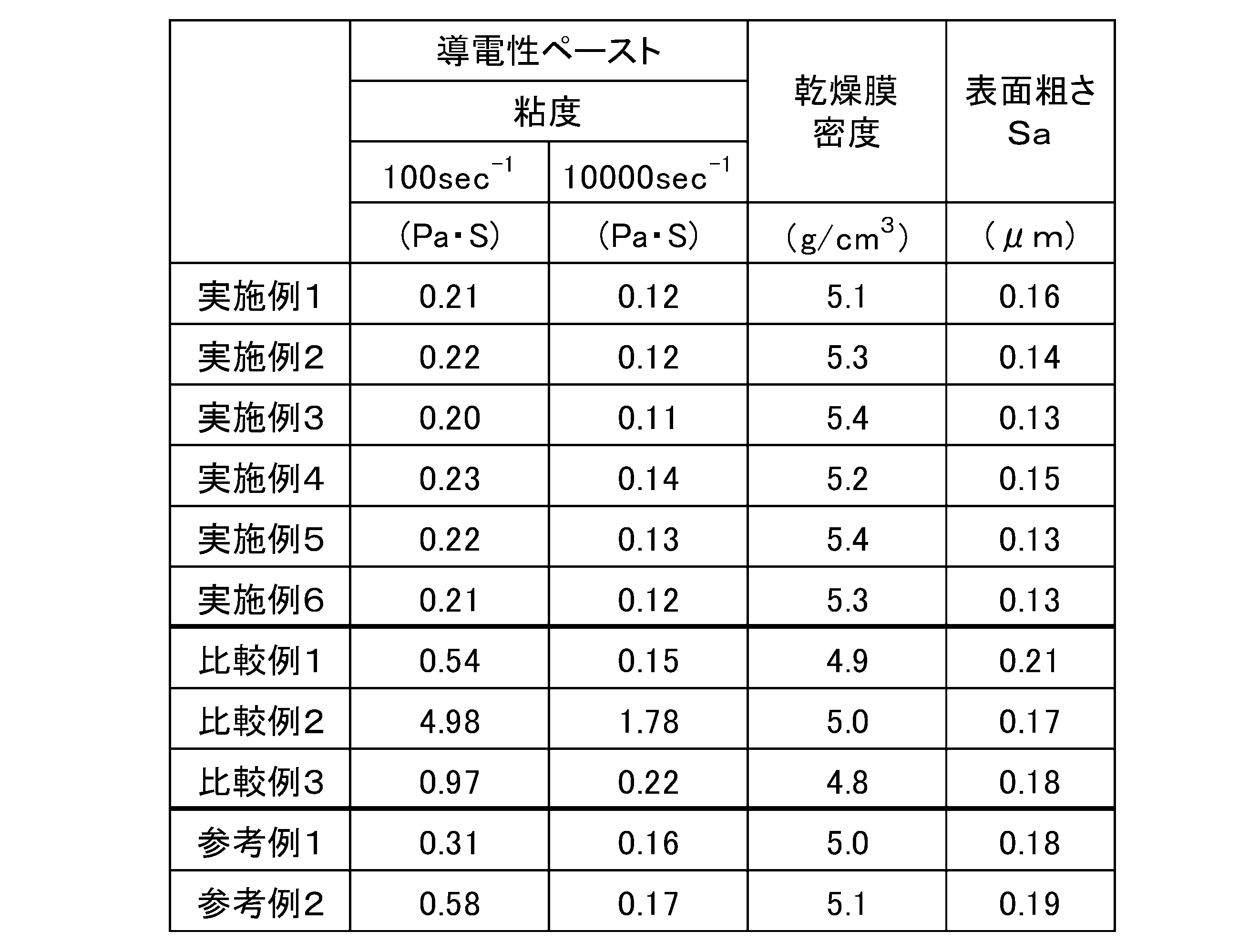
実施例の導電性ペーストは、ずり速度が100sec-1での粘度が0.20~0.23Pa・s、ずり速度が10000sec-1での粘度が0.11~0.14Pa・sであり、いずれのずり速度でも安定して低い値を示し、グラビア印刷に適した粘度を有することが示された。また、実施例の導電性ペーストは、乾燥膜密度が5.1~5.4g/cm3と高い値を示し、かつ、乾燥膜の表面粗さが0.13~0.16μmであり、分散性に優れることが確認された。
10 セラミック積層体
11 内部電極層
12 誘電体層
20 外部電極
21 外部電極層
22 メッキ層
Claims (14)
- 導電性粉末、セラミック粉末、分散剤、バインダー樹脂及び有機溶剤を含む導電性ペーストであって、
前記分散剤は、第1の酸系分散剤及び第2の酸系分散剤を含み、
前記第1の酸系分散剤は、平均分子量が500を超え2000以下であり、かつ、主鎖に対して炭化水素基からなる分岐鎖を1つ以上有し、
前記第2の酸系分散剤は、前記第1の酸系分散剤以外で、カルボキシル基を有し、
前記バインダー樹脂は、アセタール系樹脂を含み、
前記有機溶剤は、グリコールエーテル系溶剤を含む、
導電性ペースト。 - 前記第1の酸系分散剤は、カルボキシル基を有する、請求項1に記載の導電性ペースト。
- 前記第1の酸系分散剤は、ポリカルボン酸を主鎖とする炭化水素系グラフト共重合体である、請求項1又は2に記載の導電性ペースト。
- 前記第2の酸系分散剤は、分子量が5000以下であり、かつ、炭素数10以上20以下のアルキル基又は炭素数10以上20以下のアルケニル基を含む、請求項1~3のいずれか一項に記載の導電性ペースト。
- 前記第1の酸系分散剤は、前記導電性粉末100質量部に対して、0.2質量部以上2質量部以下含有され、前記第2の酸系分散剤は、前記導電性粉末100質量部に対して、0.01質量部以上2質量部以下含有される、請求項1~4のいずれか一項に記載の導電性ペースト。
- 前記導電性粉末は、Ni、Pd、Pt、Au、Ag、Cu及びこれらの合金から選ばれる少なくとも1種の金属粉末を含む、請求項1~5のいずれか一項に記載の導電性ペースト。
- 前記導電性粉末は、平均粒径が0.05μm以上1.0μm以下である、請求項1~6のいずれか一項に記載の導電性ペースト。
- 前記セラミック粉末は、ペロブスカイト型酸化物を含む、請求項1~7のいずれか一項に記載の導電性ペースト。
- 前記セラミック粉末は、平均粒径が0.01μm以上0.5μm以下である、請求項1~8のいずれか一項に記載の導電性ペースト。
- 前記バインダー樹脂が、ブチラール系樹脂を含む、請求項1~9のいずれか一項に記載の導電性ペースト。
- ずり速度100sec-1での粘度が0.8Pa・S以下であり、ずり速度10000sec-1での粘度が0.18Pa・S以下である、請求項1~10のいずれか一項に記載の導電性ペースト。
- 積層セラミック部品の内部電極用である、請求項1~11のいずれか一項に記載の導電性ペースト。
- 請求項1~11のいずれか一項に記載の導電性ペーストを用いて形成される電子部品。
- 誘電体層と内部電極とを積層した積層体を少なくとも有し、
前記内部電極は、請求項12に記載の導電性ペーストを用いて形成さる積層セラミックコンデンサ。
Priority Applications (4)
| Application Number | Priority Date | Filing Date | Title |
|---|---|---|---|
| JP2020562938A JP7405098B2 (ja) | 2018-12-25 | 2019-11-22 | 導電性ペースト、電子部品、及び積層セラミックコンデンサ |
| CN201980085792.8A CN113227233B (zh) | 2018-12-25 | 2019-11-22 | 导电性浆料、电子部件以及叠层陶瓷电容器 |
| MYPI2021003517A MY209180A (en) | 2018-12-25 | 2019-11-22 | Conductive paste, electronic component, and laminated ceramic capacitor |
| KR1020217012061A KR102773146B1 (ko) | 2018-12-25 | 2019-11-22 | 도전성 페이스트, 전자 부품, 및 적층 세라믹 콘덴서 |
Applications Claiming Priority (2)
| Application Number | Priority Date | Filing Date | Title |
|---|---|---|---|
| JP2018241705 | 2018-12-25 | ||
| JP2018-241705 | 2018-12-25 |
Publications (1)
| Publication Number | Publication Date |
|---|---|
| WO2020137289A1 true WO2020137289A1 (ja) | 2020-07-02 |
Family
ID=71126231
Family Applications (1)
| Application Number | Title | Priority Date | Filing Date |
|---|---|---|---|
| PCT/JP2019/045824 Ceased WO2020137289A1 (ja) | 2018-12-25 | 2019-11-22 | 導電性ペースト、電子部品、及び積層セラミックコンデンサ |
Country Status (5)
| Country | Link |
|---|---|
| JP (1) | JP7405098B2 (ja) |
| KR (1) | KR102773146B1 (ja) |
| CN (1) | CN113227233B (ja) |
| MY (1) | MY209180A (ja) |
| WO (1) | WO2020137289A1 (ja) |
Cited By (5)
| Publication number | Priority date | Publication date | Assignee | Title |
|---|---|---|---|---|
| WO2022168446A1 (ja) * | 2021-02-02 | 2022-08-11 | 株式会社村田製作所 | 無機粒子含有ペースト、無機粒子含有膜、及び積層体 |
| WO2024062857A1 (ja) * | 2022-09-21 | 2024-03-28 | 住友金属鉱山株式会社 | 導電性ペースト、電子部品及び積層セラミックコンデンサ |
| WO2025150392A1 (ja) * | 2024-01-09 | 2025-07-17 | 住友金属鉱山株式会社 | 導電性ペースト、電子部品及び積層セラミックコンデンサ |
| WO2025150391A1 (ja) * | 2024-01-09 | 2025-07-17 | 住友金属鉱山株式会社 | 導電性ペースト、電子部品及び積層セラミックコンデンサ |
| WO2025150393A1 (ja) * | 2024-01-09 | 2025-07-17 | 住友金属鉱山株式会社 | ビヒクル、導電性ペースト、電子部品及び積層セラミックコンデンサ |
Families Citing this family (2)
| Publication number | Priority date | Publication date | Assignee | Title |
|---|---|---|---|---|
| CN112322099B (zh) * | 2020-10-21 | 2024-11-12 | 河北银隆新能源有限公司 | 底涂浆料、电池极片及电池极片的制备方法、电池 |
| JP7540459B2 (ja) * | 2022-05-09 | 2024-08-27 | 昭栄化学工業株式会社 | ポリマー型導電性ペースト、導電膜、及び、固体電解コンデンサ素子 |
Citations (3)
| Publication number | Priority date | Publication date | Assignee | Title |
|---|---|---|---|---|
| JP2012174797A (ja) * | 2011-02-18 | 2012-09-10 | Sumitomo Metal Mining Co Ltd | 積層セラミックコンデンサ内部電極に用いられるグラビア印刷用導電性ペースト |
| JP2016147261A (ja) * | 2015-02-06 | 2016-08-18 | 日油株式会社 | 非水系分散剤および非水系分散体組成物 |
| WO2018061891A1 (ja) * | 2016-09-27 | 2018-04-05 | 富士フイルム株式会社 | 分散液、組成物、膜、膜の製造方法および分散剤 |
Family Cites Families (11)
| Publication number | Priority date | Publication date | Assignee | Title |
|---|---|---|---|---|
| JP4389431B2 (ja) | 2001-12-13 | 2009-12-24 | 株式会社村田製作所 | グラビア印刷用導電性ペーストおよびその製造方法、ならびに積層セラミック電子部品 |
| JP2003187638A (ja) | 2001-12-20 | 2003-07-04 | Murata Mfg Co Ltd | グラビア印刷用導電性ペーストおよびその製造方法、ならびに積層セラミック電子部品 |
| KR20090125393A (ko) * | 2008-06-02 | 2009-12-07 | 주식회사 동진쎄미켐 | 흑색 도전성 페이스트 조성물, 이를 포함하는 전자파차폐용 필터 및 표시 장치 |
| JP5833969B2 (ja) * | 2012-04-27 | 2015-12-16 | 富士フイルム株式会社 | 感放射線性組成物、遮光膜および固体撮像素子 |
| JP2015133317A (ja) * | 2013-12-10 | 2015-07-23 | Dowaエレクトロニクス株式会社 | 導電性ペーストおよびそれを用いた導電膜の製造方法 |
| JP6277751B2 (ja) * | 2014-02-04 | 2018-02-14 | 大日本印刷株式会社 | 銅粒子分散ペースト、及び導電性基板の製造方法 |
| JP6361356B2 (ja) * | 2014-07-30 | 2018-07-25 | 住友金属鉱山株式会社 | 積層セラミックコンデンサ内部電極用ペースト、及び積層セラミックコンデンサ |
| JP6314728B2 (ja) * | 2014-07-30 | 2018-04-25 | 住友金属鉱山株式会社 | 導電性ペーストの製造方法及びこれにより得られる導電性ペースト |
| KR102410080B1 (ko) * | 2014-07-31 | 2022-06-16 | 스미토모 긴조쿠 고잔 가부시키가이샤 | 도전성 페이스트 |
| JP6939015B2 (ja) * | 2017-03-29 | 2021-09-22 | 住友金属鉱山株式会社 | 積層セラミックコンデンサ内部電極用のグラビア印刷用導電性ペースト |
| JP6719539B2 (ja) * | 2018-12-13 | 2020-07-08 | 株式会社ノリタケカンパニーリミテド | 導電性ペースト |
-
2019
- 2019-11-22 WO PCT/JP2019/045824 patent/WO2020137289A1/ja not_active Ceased
- 2019-11-22 MY MYPI2021003517A patent/MY209180A/en unknown
- 2019-11-22 CN CN201980085792.8A patent/CN113227233B/zh active Active
- 2019-11-22 KR KR1020217012061A patent/KR102773146B1/ko active Active
- 2019-11-22 JP JP2020562938A patent/JP7405098B2/ja active Active
Patent Citations (3)
| Publication number | Priority date | Publication date | Assignee | Title |
|---|---|---|---|---|
| JP2012174797A (ja) * | 2011-02-18 | 2012-09-10 | Sumitomo Metal Mining Co Ltd | 積層セラミックコンデンサ内部電極に用いられるグラビア印刷用導電性ペースト |
| JP2016147261A (ja) * | 2015-02-06 | 2016-08-18 | 日油株式会社 | 非水系分散剤および非水系分散体組成物 |
| WO2018061891A1 (ja) * | 2016-09-27 | 2018-04-05 | 富士フイルム株式会社 | 分散液、組成物、膜、膜の製造方法および分散剤 |
Cited By (5)
| Publication number | Priority date | Publication date | Assignee | Title |
|---|---|---|---|---|
| WO2022168446A1 (ja) * | 2021-02-02 | 2022-08-11 | 株式会社村田製作所 | 無機粒子含有ペースト、無機粒子含有膜、及び積層体 |
| WO2024062857A1 (ja) * | 2022-09-21 | 2024-03-28 | 住友金属鉱山株式会社 | 導電性ペースト、電子部品及び積層セラミックコンデンサ |
| WO2025150392A1 (ja) * | 2024-01-09 | 2025-07-17 | 住友金属鉱山株式会社 | 導電性ペースト、電子部品及び積層セラミックコンデンサ |
| WO2025150391A1 (ja) * | 2024-01-09 | 2025-07-17 | 住友金属鉱山株式会社 | 導電性ペースト、電子部品及び積層セラミックコンデンサ |
| WO2025150393A1 (ja) * | 2024-01-09 | 2025-07-17 | 住友金属鉱山株式会社 | ビヒクル、導電性ペースト、電子部品及び積層セラミックコンデンサ |
Also Published As
| Publication number | Publication date |
|---|---|
| MY209180A (en) | 2025-06-26 |
| JP7405098B2 (ja) | 2023-12-26 |
| CN113227233A (zh) | 2021-08-06 |
| CN113227233B (zh) | 2023-12-12 |
| JPWO2020137289A1 (ja) | 2021-11-04 |
| KR20210110285A (ko) | 2021-09-07 |
| KR102773146B1 (ko) | 2025-02-25 |
| TW202034353A (zh) | 2020-09-16 |
Similar Documents
| Publication | Publication Date | Title |
|---|---|---|
| JP7279643B2 (ja) | 導電性ペースト、電子部品、及び積層セラミックコンデンサ | |
| JP7498896B2 (ja) | 導電性ペースト、電子部品、及び積層セラミックコンデンサ | |
| JP7405098B2 (ja) | 導電性ペースト、電子部品、及び積層セラミックコンデンサ | |
| JP7750318B2 (ja) | 導電性ペースト、電子部品、及び積層セラミックコンデンサ | |
| KR102731211B1 (ko) | 도전성 페이스트, 전자 부품, 및 적층 세라믹 콘덴서 | |
| TWI801445B (zh) | 導電性漿料、電子零件以及層積陶瓷電容器 | |
| JP2012174797A (ja) | 積層セラミックコンデンサ内部電極に用いられるグラビア印刷用導電性ペースト | |
| JP7279642B2 (ja) | 導電性ペースト、電子部品、及び積層セラミックコンデンサ | |
| CN111066098B (zh) | 导电性浆料、电子部件以及叠层陶瓷电容器 | |
| WO2019043674A2 (ja) | 導電性ペースト、電子部品、及び積層セラミックコンデンサ | |
| TW201939522A (zh) | 導電性漿料、電子零件以及層積陶瓷電容器 | |
| JP7206671B2 (ja) | 導電性ペースト、電子部品及び積層セラミックコンデンサ | |
| WO2022255467A1 (ja) | グラビア印刷用導電性ペースト、電子部品、及び積層セラミックコンデンサ | |
| JP7586088B2 (ja) | 導電性組成物、導電性ペースト、電子部品、及び積層セラミックコンデンサ | |
| WO2019043672A2 (ja) | 導電性ペースト、電子部品及び積層セラミックコンデンサ | |
| WO2019043673A2 (ja) | 導電性ペースト、電子部品、及び積層セラミックコンデンサ |
Legal Events
| Date | Code | Title | Description |
|---|---|---|---|
| 121 | Ep: the epo has been informed by wipo that ep was designated in this application |
Ref document number: 19905602 Country of ref document: EP Kind code of ref document: A1 |
|
| ENP | Entry into the national phase |
Ref document number: 20217012061 Country of ref document: KR Kind code of ref document: A |
|
| ENP | Entry into the national phase |
Ref document number: 2020562938 Country of ref document: JP Kind code of ref document: A |
|
| NENP | Non-entry into the national phase |
Ref country code: DE |
|
| 122 | Ep: pct application non-entry in european phase |
Ref document number: 19905602 Country of ref document: EP Kind code of ref document: A1 |