WO2019043672A2 - 導電性ペースト、電子部品及び積層セラミックコンデンサ - Google Patents
導電性ペースト、電子部品及び積層セラミックコンデンサ Download PDFInfo
- Publication number
- WO2019043672A2 WO2019043672A2 PCT/IB2018/058471 IB2018058471W WO2019043672A2 WO 2019043672 A2 WO2019043672 A2 WO 2019043672A2 IB 2018058471 W IB2018058471 W IB 2018058471W WO 2019043672 A2 WO2019043672 A2 WO 2019043672A2
- Authority
- WO
- WIPO (PCT)
- Prior art keywords
- conductive paste
- mass
- dispersant
- parts
- conductive
- Prior art date
Links
- 239000003985 ceramic capacitor Substances 0.000 title claims description 29
- 239000002270 dispersing agent Substances 0.000 claims abstract description 137
- 239000000843 powder Substances 0.000 claims abstract description 91
- 229920005989 resin Polymers 0.000 claims abstract description 50
- 239000011347 resin Substances 0.000 claims abstract description 50
- 239000003960 organic solvent Substances 0.000 claims abstract description 46
- 150000001413 amino acids Chemical class 0.000 claims abstract description 43
- 239000011230 binding agent Substances 0.000 claims abstract description 43
- MTHSVFCYNBDYFN-UHFFFAOYSA-N diethylene glycol Chemical compound OCCOCCO MTHSVFCYNBDYFN-UHFFFAOYSA-N 0.000 claims abstract description 16
- DHKHKXVYLBGOIT-UHFFFAOYSA-N 1,1-Diethoxyethane Chemical compound CCOC(C)OCC DHKHKXVYLBGOIT-UHFFFAOYSA-N 0.000 claims abstract description 11
- 239000011354 acetal resin Substances 0.000 claims abstract description 8
- 229920006324 polyoxymethylene Polymers 0.000 claims abstract description 8
- 239000000919 ceramic Substances 0.000 claims description 46
- 239000002245 particle Substances 0.000 claims description 21
- 125000004432 carbon atom Chemical group C* 0.000 claims description 8
- 239000000956 alloy Substances 0.000 claims description 7
- 229910045601 alloy Inorganic materials 0.000 claims description 7
- 239000004210 ether based solvent Substances 0.000 claims description 7
- 125000000217 alkyl group Chemical group 0.000 claims description 6
- 229910052751 metal Inorganic materials 0.000 claims description 6
- 239000002184 metal Substances 0.000 claims description 6
- 229910052759 nickel Inorganic materials 0.000 claims description 6
- 125000003342 alkenyl group Chemical group 0.000 claims description 5
- 229910052802 copper Inorganic materials 0.000 claims description 5
- 229910052763 palladium Inorganic materials 0.000 claims description 4
- 229910052697 platinum Inorganic materials 0.000 claims description 4
- 229910052709 silver Inorganic materials 0.000 claims description 4
- 229910052737 gold Inorganic materials 0.000 claims description 3
- 239000002904 solvent Substances 0.000 abstract description 38
- 238000007646 gravure printing Methods 0.000 abstract description 21
- 238000011156 evaluation Methods 0.000 description 20
- -1 for example Substances 0.000 description 16
- PXHVJJICTQNCMI-UHFFFAOYSA-N Nickel Chemical compound [Ni] PXHVJJICTQNCMI-UHFFFAOYSA-N 0.000 description 15
- QTBSBXVTEAMEQO-UHFFFAOYSA-M Acetate Chemical compound CC([O-])=O QTBSBXVTEAMEQO-UHFFFAOYSA-M 0.000 description 14
- 238000000034 method Methods 0.000 description 14
- NBIIXXVUZAFLBC-UHFFFAOYSA-N Phosphoric acid Chemical compound OP(O)(O)=O NBIIXXVUZAFLBC-UHFFFAOYSA-N 0.000 description 12
- 230000000052 comparative effect Effects 0.000 description 12
- 239000002253 acid Substances 0.000 description 11
- RWNUSVWFHDHRCJ-UHFFFAOYSA-N 1-butoxypropan-2-ol Chemical compound CCCCOCC(C)O RWNUSVWFHDHRCJ-UHFFFAOYSA-N 0.000 description 10
- 238000007639 printing Methods 0.000 description 10
- 239000001856 Ethyl cellulose Substances 0.000 description 9
- ZZSNKZQZMQGXPY-UHFFFAOYSA-N Ethyl cellulose Chemical compound CCOCC1OC(OC)C(OCC)C(OCC)C1OC1C(O)C(O)C(OC)C(CO)O1 ZZSNKZQZMQGXPY-UHFFFAOYSA-N 0.000 description 9
- 229920001249 ethyl cellulose Polymers 0.000 description 9
- 235000019325 ethyl cellulose Nutrition 0.000 description 9
- WUOACPNHFRMFPN-UHFFFAOYSA-N alpha-terpineol Chemical compound CC1=CCC(C(C)(C)O)CC1 WUOACPNHFRMFPN-UHFFFAOYSA-N 0.000 description 8
- SQIFACVGCPWBQZ-UHFFFAOYSA-N delta-terpineol Natural products CC(C)(O)C1CCC(=C)CC1 SQIFACVGCPWBQZ-UHFFFAOYSA-N 0.000 description 8
- 238000001035 drying Methods 0.000 description 8
- 229940116411 terpineol Drugs 0.000 description 8
- DNIAPMSPPWPWGF-UHFFFAOYSA-N Propylene glycol Chemical compound CC(O)CO DNIAPMSPPWPWGF-UHFFFAOYSA-N 0.000 description 7
- 239000012298 atmosphere Substances 0.000 description 7
- 229920002037 poly(vinyl butyral) polymer Polymers 0.000 description 7
- 150000001338 aliphatic hydrocarbons Chemical class 0.000 description 6
- 229910000147 aluminium phosphate Inorganic materials 0.000 description 6
- 229910002113 barium titanate Inorganic materials 0.000 description 6
- JRPBQTZRNDNNOP-UHFFFAOYSA-N barium titanate Chemical compound [Ba+2].[Ba+2].[O-][Ti]([O-])([O-])[O-] JRPBQTZRNDNNOP-UHFFFAOYSA-N 0.000 description 6
- 239000000203 mixture Substances 0.000 description 6
- 238000004519 manufacturing process Methods 0.000 description 5
- 125000003178 carboxy group Chemical group [H]OC(*)=O 0.000 description 4
- 239000010949 copper Substances 0.000 description 4
- JRBPAEWTRLWTQC-UHFFFAOYSA-N dodecylamine Chemical compound CCCCCCCCCCCCN JRBPAEWTRLWTQC-UHFFFAOYSA-N 0.000 description 4
- 238000010304 firing Methods 0.000 description 4
- QGLWBTPVKHMVHM-KTKRTIGZSA-N (z)-octadec-9-en-1-amine Chemical compound CCCCCCCC\C=C/CCCCCCCCN QGLWBTPVKHMVHM-KTKRTIGZSA-N 0.000 description 3
- ZWEHNKRNPOVVGH-UHFFFAOYSA-N 2-Butanone Chemical compound CCC(C)=O ZWEHNKRNPOVVGH-UHFFFAOYSA-N 0.000 description 3
- WWJLCYHYLZZXBE-UHFFFAOYSA-N 5-chloro-1,3-dihydroindol-2-one Chemical compound ClC1=CC=C2NC(=O)CC2=C1 WWJLCYHYLZZXBE-UHFFFAOYSA-N 0.000 description 3
- XEKOWRVHYACXOJ-UHFFFAOYSA-N Ethyl acetate Chemical compound CCOC(C)=O XEKOWRVHYACXOJ-UHFFFAOYSA-N 0.000 description 3
- KGEKLUUHTZCSIP-UHFFFAOYSA-N Isobornyl acetate Natural products C1CC2(C)C(OC(=O)C)CC1C2(C)C KGEKLUUHTZCSIP-UHFFFAOYSA-N 0.000 description 3
- 239000002202 Polyethylene glycol Substances 0.000 description 3
- 239000001940 [(1R,4S,6R)-1,7,7-trimethyl-6-bicyclo[2.2.1]heptanyl] acetate Substances 0.000 description 3
- 150000001241 acetals Chemical class 0.000 description 3
- 239000000654 additive Substances 0.000 description 3
- 125000004429 atom Chemical group 0.000 description 3
- 229910052788 barium Inorganic materials 0.000 description 3
- 239000004020 conductor Substances 0.000 description 3
- 239000006185 dispersion Substances 0.000 description 3
- 239000012530 fluid Substances 0.000 description 3
- 229910052500 inorganic mineral Inorganic materials 0.000 description 3
- 239000011707 mineral Substances 0.000 description 3
- 239000012046 mixed solvent Substances 0.000 description 3
- 229920001223 polyethylene glycol Polymers 0.000 description 3
- 230000008569 process Effects 0.000 description 3
- 239000002994 raw material Substances 0.000 description 3
- 150000003839 salts Chemical class 0.000 description 3
- 239000004094 surface-active agent Substances 0.000 description 3
- 230000009974 thixotropic effect Effects 0.000 description 3
- WRIDQFICGBMAFQ-UHFFFAOYSA-N (E)-8-Octadecenoic acid Natural products CCCCCCCCCC=CCCCCCCC(O)=O WRIDQFICGBMAFQ-UHFFFAOYSA-N 0.000 description 2
- LAVARTIQQDZFNT-UHFFFAOYSA-N 1-(1-methoxypropan-2-yloxy)propan-2-yl acetate Chemical compound COCC(C)OCC(C)OC(C)=O LAVARTIQQDZFNT-UHFFFAOYSA-N 0.000 description 2
- HBNHCGDYYBMKJN-UHFFFAOYSA-N 2-(4-methylcyclohexyl)propan-2-yl acetate Chemical compound CC1CCC(C(C)(C)OC(C)=O)CC1 HBNHCGDYYBMKJN-UHFFFAOYSA-N 0.000 description 2
- NQBXSWAWVZHKBZ-UHFFFAOYSA-N 2-butoxyethyl acetate Chemical compound CCCCOCCOC(C)=O NQBXSWAWVZHKBZ-UHFFFAOYSA-N 0.000 description 2
- LQJBNNIYVWPHFW-UHFFFAOYSA-N 20:1omega9c fatty acid Natural products CCCCCCCCCCC=CCCCCCCCC(O)=O LQJBNNIYVWPHFW-UHFFFAOYSA-N 0.000 description 2
- QSBYPNXLFMSGKH-UHFFFAOYSA-N 9-Heptadecensaeure Natural products CCCCCCCC=CCCCCCCCC(O)=O QSBYPNXLFMSGKH-UHFFFAOYSA-N 0.000 description 2
- RSWGJHLUYNHPMX-UHFFFAOYSA-N Abietic-Saeure Natural products C12CCC(C(C)C)=CC2=CCC2C1(C)CCCC2(C)C(O)=O RSWGJHLUYNHPMX-UHFFFAOYSA-N 0.000 description 2
- FERIUCNNQQJTOY-UHFFFAOYSA-N Butyric acid Natural products CCCC(O)=O FERIUCNNQQJTOY-UHFFFAOYSA-N 0.000 description 2
- KRKIAJBQOUBNSE-GYSYKLTISA-N Isobornyl isobutyrate Chemical compound C1C[C@@]2(C)[C@H](OC(=O)C(C)C)C[C@@H]1C2(C)C KRKIAJBQOUBNSE-GYSYKLTISA-N 0.000 description 2
- 229910000990 Ni alloy Inorganic materials 0.000 description 2
- 239000005642 Oleic acid Substances 0.000 description 2
- ZQPPMHVWECSIRJ-UHFFFAOYSA-N Oleic acid Natural products CCCCCCCCC=CCCCCCCCC(O)=O ZQPPMHVWECSIRJ-UHFFFAOYSA-N 0.000 description 2
- 229920003171 Poly (ethylene oxide) Polymers 0.000 description 2
- KHPCPRHQVVSZAH-HUOMCSJISA-N Rosin Natural products O(C/C=C/c1ccccc1)[C@H]1[C@H](O)[C@@H](O)[C@@H](O)[C@@H](CO)O1 KHPCPRHQVVSZAH-HUOMCSJISA-N 0.000 description 2
- 235000021355 Stearic acid Nutrition 0.000 description 2
- FAFMZORPAAGQFV-BREBYQMCSA-N [(1r,3r,4r)-4,7,7-trimethyl-3-bicyclo[2.2.1]heptanyl] propanoate Chemical compound C1C[C@@]2(C)[C@H](OC(=O)CC)C[C@@H]1C2(C)C FAFMZORPAAGQFV-BREBYQMCSA-N 0.000 description 2
- 230000000996 additive effect Effects 0.000 description 2
- 230000002776 aggregation Effects 0.000 description 2
- 238000004220 aggregation Methods 0.000 description 2
- 150000003973 alkyl amines Chemical class 0.000 description 2
- 125000005211 alkyl trimethyl ammonium group Chemical group 0.000 description 2
- 150000001412 amines Chemical class 0.000 description 2
- 150000001732 carboxylic acid derivatives Chemical class 0.000 description 2
- 229910052804 chromium Inorganic materials 0.000 description 2
- 230000007423 decrease Effects 0.000 description 2
- 235000014113 dietary fatty acids Nutrition 0.000 description 2
- UKMSUNONTOPOIO-UHFFFAOYSA-N docosanoic acid Chemical compound CCCCCCCCCCCCCCCCCCCCCC(O)=O UKMSUNONTOPOIO-UHFFFAOYSA-N 0.000 description 2
- POULHZVOKOAJMA-UHFFFAOYSA-N dodecanoic acid Chemical compound CCCCCCCCCCCC(O)=O POULHZVOKOAJMA-UHFFFAOYSA-N 0.000 description 2
- LYCAIKOWRPUZTN-UHFFFAOYSA-N ethylene glycol Natural products OCCO LYCAIKOWRPUZTN-UHFFFAOYSA-N 0.000 description 2
- 239000000194 fatty acid Substances 0.000 description 2
- 229930195729 fatty acid Natural products 0.000 description 2
- 150000004665 fatty acids Chemical class 0.000 description 2
- 239000007789 gas Substances 0.000 description 2
- 239000011521 glass Substances 0.000 description 2
- 239000010931 gold Substances 0.000 description 2
- IPCSVZSSVZVIGE-UHFFFAOYSA-N hexadecanoic acid Chemical compound CCCCCCCCCCCCCCCC(O)=O IPCSVZSSVZVIGE-UHFFFAOYSA-N 0.000 description 2
- 239000003112 inhibitor Substances 0.000 description 2
- DIICMQCJAQLQPI-UHFFFAOYSA-N isobornyl propionate Natural products CCC(=O)C1CC2CCC1(C)C2(C)C DIICMQCJAQLQPI-UHFFFAOYSA-N 0.000 description 2
- QXJSBBXBKPUZAA-UHFFFAOYSA-N isooleic acid Natural products CCCCCCCC=CCCCCCCCCC(O)=O QXJSBBXBKPUZAA-UHFFFAOYSA-N 0.000 description 2
- 229910052748 manganese Inorganic materials 0.000 description 2
- 239000000463 material Substances 0.000 description 2
- UODXCYZDMHPIJE-UHFFFAOYSA-N menthanol Chemical compound CC1CCC(C(C)(C)O)CC1 UODXCYZDMHPIJE-UHFFFAOYSA-N 0.000 description 2
- BKIMMITUMNQMOS-UHFFFAOYSA-N nonane Chemical compound CCCCCCCCC BKIMMITUMNQMOS-UHFFFAOYSA-N 0.000 description 2
- QIQXTHQIDYTFRH-UHFFFAOYSA-N octadecanoic acid Chemical compound CCCCCCCCCCCCCCCCCC(O)=O QIQXTHQIDYTFRH-UHFFFAOYSA-N 0.000 description 2
- OQCDKBAXFALNLD-UHFFFAOYSA-N octadecanoic acid Natural products CCCCCCCC(C)CCCCCCCCC(O)=O OQCDKBAXFALNLD-UHFFFAOYSA-N 0.000 description 2
- ZQPPMHVWECSIRJ-KTKRTIGZSA-N oleic acid Chemical compound CCCCCCCC\C=C/CCCCCCCC(O)=O ZQPPMHVWECSIRJ-KTKRTIGZSA-N 0.000 description 2
- KDLHZDBZIXYQEI-UHFFFAOYSA-N palladium Substances [Pd] KDLHZDBZIXYQEI-UHFFFAOYSA-N 0.000 description 2
- 238000007747 plating Methods 0.000 description 2
- BASFCYQUMIYNBI-UHFFFAOYSA-N platinum Substances [Pt] BASFCYQUMIYNBI-UHFFFAOYSA-N 0.000 description 2
- 229920000642 polymer Polymers 0.000 description 2
- 229910052761 rare earth metal Inorganic materials 0.000 description 2
- 238000007650 screen-printing Methods 0.000 description 2
- 238000000926 separation method Methods 0.000 description 2
- 239000010944 silver (metal) Substances 0.000 description 2
- 239000007787 solid Substances 0.000 description 2
- 239000008117 stearic acid Substances 0.000 description 2
- 239000000758 substrate Substances 0.000 description 2
- KHPCPRHQVVSZAH-UHFFFAOYSA-N trans-cinnamyl beta-D-glucopyranoside Natural products OC1C(O)C(O)C(CO)OC1OCC=CC1=CC=CC=C1 KHPCPRHQVVSZAH-UHFFFAOYSA-N 0.000 description 2
- IIYFAKIEWZDVMP-UHFFFAOYSA-N tridecane Chemical compound CCCCCCCCCCCCC IIYFAKIEWZDVMP-UHFFFAOYSA-N 0.000 description 2
- XFNJVJPLKCPIBV-UHFFFAOYSA-N trimethylenediamine Chemical compound NCCCN XFNJVJPLKCPIBV-UHFFFAOYSA-N 0.000 description 2
- LNAZSHAWQACDHT-XIYTZBAFSA-N (2r,3r,4s,5r,6s)-4,5-dimethoxy-2-(methoxymethyl)-3-[(2s,3r,4s,5r,6r)-3,4,5-trimethoxy-6-(methoxymethyl)oxan-2-yl]oxy-6-[(2r,3r,4s,5r,6r)-4,5,6-trimethoxy-2-(methoxymethyl)oxan-3-yl]oxyoxane Chemical compound CO[C@@H]1[C@@H](OC)[C@H](OC)[C@@H](COC)O[C@H]1O[C@H]1[C@H](OC)[C@@H](OC)[C@H](O[C@H]2[C@@H]([C@@H](OC)[C@H](OC)O[C@@H]2COC)OC)O[C@@H]1COC LNAZSHAWQACDHT-XIYTZBAFSA-N 0.000 description 1
- OYHQOLUKZRVURQ-NTGFUMLPSA-N (9Z,12Z)-9,10,12,13-tetratritiooctadeca-9,12-dienoic acid Chemical compound C(CCCCCCC\C(=C(/C\C(=C(/CCCCC)\[3H])\[3H])\[3H])\[3H])(=O)O OYHQOLUKZRVURQ-NTGFUMLPSA-N 0.000 description 1
- FJLUATLTXUNBOT-UHFFFAOYSA-N 1-Hexadecylamine Chemical compound CCCCCCCCCCCCCCCCN FJLUATLTXUNBOT-UHFFFAOYSA-N 0.000 description 1
- JOLQKTGDSGKSKJ-UHFFFAOYSA-N 1-ethoxypropan-2-ol Chemical compound CCOCC(C)O JOLQKTGDSGKSKJ-UHFFFAOYSA-N 0.000 description 1
- OHJYHAOODFPJOD-UHFFFAOYSA-N 2-(2-ethylhexoxy)ethanol Chemical compound CCCCC(CC)COCCO OHJYHAOODFPJOD-UHFFFAOYSA-N 0.000 description 1
- GZMAAYIALGURDQ-UHFFFAOYSA-N 2-(2-hexoxyethoxy)ethanol Chemical compound CCCCCCOCCOCCO GZMAAYIALGURDQ-UHFFFAOYSA-N 0.000 description 1
- OADIZUFHUPTFAG-UHFFFAOYSA-N 2-[2-(2-ethylhexoxy)ethoxy]ethanol Chemical compound CCCCC(CC)COCCOCCO OADIZUFHUPTFAG-UHFFFAOYSA-N 0.000 description 1
- UPGSWASWQBLSKZ-UHFFFAOYSA-N 2-hexoxyethanol Chemical compound CCCCCCOCCO UPGSWASWQBLSKZ-UHFFFAOYSA-N 0.000 description 1
- 125000000954 2-hydroxyethyl group Chemical group [H]C([*])([H])C([H])([H])O[H] 0.000 description 1
- LDMRLRNXHLPZJN-UHFFFAOYSA-N 3-propoxypropan-1-ol Chemical compound CCCOCCCO LDMRLRNXHLPZJN-UHFFFAOYSA-N 0.000 description 1
- 229920000178 Acrylic resin Polymers 0.000 description 1
- 239000004925 Acrylic resin Substances 0.000 description 1
- 229910018072 Al 2 O 3 Inorganic materials 0.000 description 1
- NLXLAEXVIDQMFP-UHFFFAOYSA-N Ammonium chloride Substances [NH4+].[Cl-] NLXLAEXVIDQMFP-UHFFFAOYSA-N 0.000 description 1
- 235000021357 Behenic acid Nutrition 0.000 description 1
- 229910015902 Bi 2 O 3 Inorganic materials 0.000 description 1
- 229920002799 BoPET Polymers 0.000 description 1
- DKPFZGUDAPQIHT-UHFFFAOYSA-N Butyl acetate Natural products CCCCOC(C)=O DKPFZGUDAPQIHT-UHFFFAOYSA-N 0.000 description 1
- ZTQSAGDEMFDKMZ-UHFFFAOYSA-N Butyraldehyde Chemical compound CCCC=O ZTQSAGDEMFDKMZ-UHFFFAOYSA-N 0.000 description 1
- RYGMFSIKBFXOCR-UHFFFAOYSA-N Copper Chemical compound [Cu] RYGMFSIKBFXOCR-UHFFFAOYSA-N 0.000 description 1
- XDTMQSROBMDMFD-UHFFFAOYSA-N Cyclohexane Chemical compound C1CCCCC1 XDTMQSROBMDMFD-UHFFFAOYSA-N 0.000 description 1
- LCGLNKUTAGEVQW-UHFFFAOYSA-N Dimethyl ether Chemical compound COC LCGLNKUTAGEVQW-UHFFFAOYSA-N 0.000 description 1
- 229920000896 Ethulose Polymers 0.000 description 1
- 239000001859 Ethyl hydroxyethyl cellulose Substances 0.000 description 1
- 239000005639 Lauric acid Substances 0.000 description 1
- NTIZESTWPVYFNL-UHFFFAOYSA-N Methyl isobutyl ketone Chemical compound CC(C)CC(C)=O NTIZESTWPVYFNL-UHFFFAOYSA-N 0.000 description 1
- UIHCLUNTQKBZGK-UHFFFAOYSA-N Methyl isobutyl ketone Natural products CCC(C)C(C)=O UIHCLUNTQKBZGK-UHFFFAOYSA-N 0.000 description 1
- 229910017493 Nd 2 O 3 Inorganic materials 0.000 description 1
- 239000000020 Nitrocellulose Substances 0.000 description 1
- REYJJPSVUYRZGE-UHFFFAOYSA-N Octadecylamine Chemical compound CCCCCCCCCCCCCCCCCCN REYJJPSVUYRZGE-UHFFFAOYSA-N 0.000 description 1
- 235000021314 Palmitic acid Nutrition 0.000 description 1
- PLZVEHJLHYMBBY-UHFFFAOYSA-N Tetradecylamine Chemical compound CCCCCCCCCCCCCCN PLZVEHJLHYMBBY-UHFFFAOYSA-N 0.000 description 1
- 229910010413 TiO 2 Inorganic materials 0.000 description 1
- 239000007983 Tris buffer Substances 0.000 description 1
- 239000000853 adhesive Substances 0.000 description 1
- 230000001070 adhesive effect Effects 0.000 description 1
- DTOSIQBPPRVQHS-PDBXOOCHSA-N alpha-linolenic acid Chemical compound CC\C=C/C\C=C/C\C=C/CCCCCCCC(O)=O DTOSIQBPPRVQHS-PDBXOOCHSA-N 0.000 description 1
- 235000020661 alpha-linolenic acid Nutrition 0.000 description 1
- 229910052782 aluminium Inorganic materials 0.000 description 1
- 235000019270 ammonium chloride Nutrition 0.000 description 1
- 238000000137 annealing Methods 0.000 description 1
- QVGXLLKOCUKJST-UHFFFAOYSA-N atomic oxygen Chemical compound [O] QVGXLLKOCUKJST-UHFFFAOYSA-N 0.000 description 1
- QVQLCTNNEUAWMS-UHFFFAOYSA-N barium oxide Inorganic materials [Ba]=O QVQLCTNNEUAWMS-UHFFFAOYSA-N 0.000 description 1
- 229940116226 behenic acid Drugs 0.000 description 1
- 229910052791 calcium Inorganic materials 0.000 description 1
- 229910052799 carbon Inorganic materials 0.000 description 1
- 239000012461 cellulose resin Substances 0.000 description 1
- 230000008859 change Effects 0.000 description 1
- 238000002485 combustion reaction Methods 0.000 description 1
- 230000008602 contraction Effects 0.000 description 1
- 238000005260 corrosion Methods 0.000 description 1
- 230000007797 corrosion Effects 0.000 description 1
- 239000006184 cosolvent Substances 0.000 description 1
- 238000000354 decomposition reaction Methods 0.000 description 1
- 150000004985 diamines Chemical class 0.000 description 1
- NAPSCFZYZVSQHF-UHFFFAOYSA-N dimantine Chemical compound CCCCCCCCCCCCCCCCCCN(C)C NAPSCFZYZVSQHF-UHFFFAOYSA-N 0.000 description 1
- 229950010007 dimantine Drugs 0.000 description 1
- 230000000694 effects Effects 0.000 description 1
- 239000002003 electrode paste Substances 0.000 description 1
- 125000001301 ethoxy group Chemical group [H]C([H])([H])C([H])([H])O* 0.000 description 1
- 235000019326 ethyl hydroxyethyl cellulose Nutrition 0.000 description 1
- 230000005484 gravity Effects 0.000 description 1
- FUZZWVXGSFPDMH-UHFFFAOYSA-N hexanoic acid Chemical compound CCCCCC(O)=O FUZZWVXGSFPDMH-UHFFFAOYSA-N 0.000 description 1
- 229910052739 hydrogen Inorganic materials 0.000 description 1
- 239000001257 hydrogen Substances 0.000 description 1
- 230000006872 improvement Effects 0.000 description 1
- 239000004615 ingredient Substances 0.000 description 1
- 229910052742 iron Inorganic materials 0.000 description 1
- GJRQTCIYDGXPES-UHFFFAOYSA-N iso-butyl acetate Natural products CC(C)COC(C)=O GJRQTCIYDGXPES-UHFFFAOYSA-N 0.000 description 1
- FGKJLKRYENPLQH-UHFFFAOYSA-M isocaproate Chemical compound CC(C)CCC([O-])=O FGKJLKRYENPLQH-UHFFFAOYSA-M 0.000 description 1
- OQAGVSWESNCJJT-UHFFFAOYSA-N isovaleric acid methyl ester Natural products COC(=O)CC(C)C OQAGVSWESNCJJT-UHFFFAOYSA-N 0.000 description 1
- 239000005453 ketone based solvent Substances 0.000 description 1
- 238000004898 kneading Methods 0.000 description 1
- 229910052745 lead Inorganic materials 0.000 description 1
- 229910052451 lead zirconate titanate Inorganic materials 0.000 description 1
- 229960004488 linolenic acid Drugs 0.000 description 1
- KQQKGWQCNNTQJW-UHFFFAOYSA-N linolenic acid Natural products CC=CCCC=CCC=CCCCCCCCC(O)=O KQQKGWQCNNTQJW-UHFFFAOYSA-N 0.000 description 1
- 239000007788 liquid Substances 0.000 description 1
- 229910052749 magnesium Inorganic materials 0.000 description 1
- XVTQAXXMUNXFMU-UHFFFAOYSA-N methyl 2-(3-oxo-2-pyridin-2-yl-1h-pyrazol-5-yl)acetate Chemical compound N1C(CC(=O)OC)=CC(=O)N1C1=CC=CC=N1 XVTQAXXMUNXFMU-UHFFFAOYSA-N 0.000 description 1
- 229920000609 methyl cellulose Polymers 0.000 description 1
- 239000001923 methylcellulose Substances 0.000 description 1
- 235000010981 methylcellulose Nutrition 0.000 description 1
- 239000011259 mixed solution Substances 0.000 description 1
- 238000002156 mixing Methods 0.000 description 1
- WQEPLUUGTLDZJY-UHFFFAOYSA-N n-Pentadecanoic acid Natural products CCCCCCCCCCCCCCC(O)=O WQEPLUUGTLDZJY-UHFFFAOYSA-N 0.000 description 1
- YKYONYBAUNKHLG-UHFFFAOYSA-N n-Propyl acetate Natural products CCCOC(C)=O YKYONYBAUNKHLG-UHFFFAOYSA-N 0.000 description 1
- 229910052758 niobium Inorganic materials 0.000 description 1
- 229920001220 nitrocellulos Polymers 0.000 description 1
- 235000021313 oleic acid Nutrition 0.000 description 1
- 230000003287 optical effect Effects 0.000 description 1
- 230000003647 oxidation Effects 0.000 description 1
- 238000007254 oxidation reaction Methods 0.000 description 1
- 230000001590 oxidative effect Effects 0.000 description 1
- 125000006353 oxyethylene group Chemical group 0.000 description 1
- 229910052760 oxygen Inorganic materials 0.000 description 1
- 239000001301 oxygen Substances 0.000 description 1
- 239000004014 plasticizer Substances 0.000 description 1
- 229920000728 polyester Polymers 0.000 description 1
- 238000006116 polymerization reaction Methods 0.000 description 1
- 229920001451 polypropylene glycol Polymers 0.000 description 1
- 238000002360 preparation method Methods 0.000 description 1
- 125000002924 primary amino group Chemical group [H]N([H])* 0.000 description 1
- 229940090181 propyl acetate Drugs 0.000 description 1
- LLHKCFNBLRBOGN-UHFFFAOYSA-N propylene glycol methyl ether acetate Chemical compound COCC(C)OC(C)=O LLHKCFNBLRBOGN-UHFFFAOYSA-N 0.000 description 1
- AOHJOMMDDJHIJH-UHFFFAOYSA-N propylenediamine Chemical compound CC(N)CN AOHJOMMDDJHIJH-UHFFFAOYSA-N 0.000 description 1
- 230000001681 protective effect Effects 0.000 description 1
- 150000003242 quaternary ammonium salts Chemical class 0.000 description 1
- 230000009467 reduction Effects 0.000 description 1
- 238000010405 reoxidation reaction Methods 0.000 description 1
- 229920006395 saturated elastomer Polymers 0.000 description 1
- 229910052710 silicon Inorganic materials 0.000 description 1
- 238000005245 sintering Methods 0.000 description 1
- 235000015096 spirit Nutrition 0.000 description 1
- 238000003756 stirring Methods 0.000 description 1
- 239000000126 substance Substances 0.000 description 1
- 229910052715 tantalum Inorganic materials 0.000 description 1
- 150000003505 terpenes Chemical class 0.000 description 1
- 235000007586 terpenes Nutrition 0.000 description 1
- 150000003512 tertiary amines Chemical class 0.000 description 1
- TUNFSRHWOTWDNC-HKGQFRNVSA-N tetradecanoic acid Chemical compound CCCCCCCCCCCCC[14C](O)=O TUNFSRHWOTWDNC-HKGQFRNVSA-N 0.000 description 1
- 238000005979 thermal decomposition reaction Methods 0.000 description 1
- 239000002562 thickening agent Substances 0.000 description 1
- 229910052718 tin Inorganic materials 0.000 description 1
- 229910052721 tungsten Inorganic materials 0.000 description 1
- NQPDZGIKBAWPEJ-UHFFFAOYSA-N valeric acid Chemical compound CCCCC(O)=O NQPDZGIKBAWPEJ-UHFFFAOYSA-N 0.000 description 1
- 229910052720 vanadium Inorganic materials 0.000 description 1
- 229910052725 zinc Inorganic materials 0.000 description 1
- XLOMVQKBTHCTTD-UHFFFAOYSA-N zinc oxide Inorganic materials [Zn]=O XLOMVQKBTHCTTD-UHFFFAOYSA-N 0.000 description 1
- 229910052726 zirconium Inorganic materials 0.000 description 1
- 229910000859 α-Fe Inorganic materials 0.000 description 1
Images

Classifications
-
- H—ELECTRICITY
- H01—ELECTRIC ELEMENTS
- H01B—CABLES; CONDUCTORS; INSULATORS; SELECTION OF MATERIALS FOR THEIR CONDUCTIVE, INSULATING OR DIELECTRIC PROPERTIES
- H01B1/00—Conductors or conductive bodies characterised by the conductive materials; Selection of materials as conductors
- H01B1/20—Conductive material dispersed in non-conductive organic material
- H01B1/22—Conductive material dispersed in non-conductive organic material the conductive material comprising metals or alloys
-
- H—ELECTRICITY
- H01—ELECTRIC ELEMENTS
- H01G—CAPACITORS; CAPACITORS, RECTIFIERS, DETECTORS, SWITCHING DEVICES, LIGHT-SENSITIVE OR TEMPERATURE-SENSITIVE DEVICES OF THE ELECTROLYTIC TYPE
- H01G4/00—Fixed capacitors; Processes of their manufacture
- H01G4/30—Stacked capacitors
Definitions
- the present invention relates to a conductive paste, an electronic component and a multilayer ceramic capacitor.
- a multilayer ceramic capacitor has a structure in which a plurality of dielectric layers and a plurality of internal electrode layers are alternately stacked, and miniaturization and high capacity can be achieved by thinning the dielectric layers and the internal electrode layers.
- the multilayer ceramic capacitor is manufactured, for example, as follows. First, a paste for an internal electrode containing a conductive powder, a binder resin, an organic solvent and the like on the surface of a dielectric green sheet containing a dielectric powder such as barium titanate (BaTiO 3 ) and a binder resin (conductive Pastes printed in a predetermined electrode pattern are stacked in multiple layers to obtain a laminate in which internal electrodes and dielectric green sheets are stacked in multiple layers. Next, this laminated body is thermocompression-bonded and integrated to form a crimped body. The pressure-bonded body is cut, subjected to a deorganic binder treatment in an oxidizing atmosphere or an inert atmosphere, and then fired to obtain a fired chip. Subsequently, the paste for external electrodes is apply
- screen printing has been generally used as a printing method to be used when printing conductive paste on a dielectric green sheet, but from the demand for miniaturization of electronic devices, reduction in thickness, and improvement in productivity. It is required to print a finer electrode pattern with high productivity.
- Gravure which is a continuous printing method in which a conductive paste is filled in a recess provided in a plate and pressed against a surface to be printed as one of the printing methods of the conductive paste, thereby transferring the conductive paste from the plate.
- a printing method has been proposed.
- the gravure printing method has a high printing speed and is excellent in productivity. In the case of using the gravure printing method, it is necessary to appropriately select the binder resin, the dispersing agent, the solvent and the like in the conductive paste to adjust the properties such as viscosity to the range suitable for the gravure printing.
- a conductive paste used to form the internal conductor film by gravure printing in a multilayer ceramic electronic component provided with a plurality of ceramic layers and an internal conductor film extending along a specific interface between the ceramic layers 30 to 70% by weight of a solid component containing metal powder, 1 to 10% by weight of an ethylcellulose resin component having an ethoxy group content of 49.6% or more, and 0.05 to 5% by weight of a dispersant And a solvent component as the remainder, and the viscosity ⁇ 0.1 at a shear rate of 0.1 (s ⁇ 1 ) is 1 Pa ⁇ s or more, and the viscosity at a shear rate of 0.02 (s ⁇ 1 )
- a conductive paste is described, which is a thixotropic fluid, with a condition that ⁇ ⁇ ⁇ ⁇ 0.02 satisfies the specific formula.
- Patent Document 2 is a conductive paste used for forming by gravure printing as in the above-mentioned Patent Document 1, and is 30 to 70% by weight of a solid component containing metal powder, and 1 to 10% by weight.
- a thixotropic fluid containing a resin component, 0.05 to 5% by weight of a dispersant, and a solvent component as the balance, and having a viscosity of 1 Pa ⁇ s or more at a shear rate of 0.1 (s ⁇ 1 ),
- a conductive paste is described in which the viscosity change rate at a shear rate of 10 (s ⁇ 1 ) is 50% or more based on the viscosity at a shear rate of 0.1 (s ⁇ 1 ).
- these conductive pastes are thixotropic fluids having a viscosity of 1 Pa ⁇ s or more at a shear rate of 0.1 (s ⁇ 1 ), and stabilized at high speed in gravure printing It is believed that continuous printability can be obtained, and multilayer ceramic electronic components such as multilayer ceramic capacitors can be manufactured with good production efficiency.
- Patent Document 3 discloses a conductive material for a laminated ceramic capacitor internal electrode including a conductive powder (A), an organic resin (B), an organic solvent (C), an additive (D), and a dielectric powder (E).
- the organic resin (B) is composed of polyvinyl butyral having a degree of polymerization of 10000 to 50000 and ethylcellulose having a weight average molecular weight of 10000 to 100000
- the organic solvent (C) is propylene glycol monobutyl ether, Or a mixed solvent of propylene glycol monobutyl ether and propylene glycol methyl ether acetate, or a mixed solvent of propylene glycol monobutyl ether and mineral spirit
- the additive (D) comprises a separation inhibitor and a dispersant, and the separation Polycarboxylic acid polymers as inhibitors Or gravure printing conductive paste made from a composition comprising a salt of a polycarboxylic acid. According to Patent Document 3, it is considered that this conductive material for
- the conductive powder With the thinning of the internal electrode layer in recent years, the conductive powder also tends to be reduced in particle size. If the particle size of the conductive powder is small, the specific surface area of the particle surface will be large, so the surface activity of the conductive powder (metal powder) may be high, and the dispersibility of the conductive paste may be lowered. A conductive paste having dispersibility is required.
- An object of the present invention is to provide a conductive paste which has a paste viscosity suitable for gravure printing and is excellent in the dispersibility and productivity of the paste.
- a first aspect of the present invention is a conductive paste containing a conductive powder, a dispersant, a binder resin, and an organic solvent, the dispersant containing an amino acid-based dispersant having a molecular weight of 5000 or less, and the binder resin
- a conductive paste is provided which contains an acetal resin and the organic solvent contains a glycol ether solvent.
- the amino acid based dispersant is preferably represented by the following general formula (1).
- R 1 is a linear alkyl group having 10 to 20 carbon atoms or a linear alkenyl group having 10 to 20 carbon atoms.
- the amino acid-based dispersant is preferably contained in an amount of 0.01 parts by mass or more and 2 parts by mass or less with respect to 100 parts by mass of the conductive powder.
- the glycol ether solvent is preferably contained in an amount of 30 parts by mass to 50 parts by mass with respect to 100 parts by mass of the conductive powder.
- the dispersant may further contain a basic dispersant.
- the dispersant is preferably contained in an amount of 0.01 parts by mass or more and 2 parts by mass or less with respect to 100 parts by mass of the conductive powder.
- the conductive powder preferably contains at least one metal powder selected from Ni, Pd, Pt, Au, Ag, Cu and alloys thereof. Further, the conductive paste preferably contains a ceramic powder. The ceramic powder preferably contains a perovskite oxide. Further, the ceramic powder preferably has an average particle diameter of 0.01 ⁇ m or more and 0.5 ⁇ m or less. The conductive powder preferably has an average particle diameter of 0.05 ⁇ m or more and 1.0 ⁇ m or less. The conductive paste is preferably for the internal electrode of the laminated ceramic component. The conductive paste, the viscosity of the shear rate 100 sec -1 is not higher than 0.8 Pa ⁇ S, it is preferable that the viscosity of the shear rate 10000 sec -1 is less than 0.18Pa ⁇ S.
- an electronic component formed using the above conductive paste.
- a multilayer ceramic capacitor comprising at least a laminate in which a dielectric layer and an internal electrode are laminated, wherein the internal electrode is formed using the conductive paste.
- the conductive paste of the present invention has a viscosity suitable for gravure printing, and is excellent in the dispersibility and productivity of the paste.
- the electrode pattern of an electronic component such as a multilayer ceramic capacitor formed by using the conductive paste of the present invention is excellent in the printability of the conductive paste and has a uniform thickness even when forming a thin-filmed electrode.
- FIG. 1 is a perspective view and a cross-sectional view showing a multilayer ceramic capacitor according to an embodiment.
- the conductive paste of the present embodiment contains a conductive powder, a dispersant, a binder resin and an organic solvent. Each component will be described in detail below.
- the conductive powder is not particularly limited, and for example, at least one powder selected from Ni, Pd, Pt, Au, Ag, Cu, and alloys thereof can be used. Among these, in view of conductivity, corrosion resistance and cost, powder of Ni or its alloy is preferable.
- the Ni alloy for example, an alloy of Ni with at least one or more elements selected from the group consisting of Mn, Cr, Co, Al, Fe, Cu, Zn, Ag, Pt, and Pd may be used. it can.
- the content of Ni in the Ni alloy is, for example, 50% by mass or more, preferably 80% by mass or more. Further, the Ni powder may contain about several hundreds ppm of S in order to suppress rapid gas generation due to partial thermal decomposition of the binder resin at the time of binder removal processing.
- the average particle diameter of the conductive powder is preferably 0.05 ⁇ m or more and 1.0 ⁇ m or less, and more preferably 0.1 ⁇ m or more and 0.5 ⁇ m or less.
- the average particle size is a value determined from observation with a scanning electron microscope (SEM), and refers to the number average value (sum of particle sizes measured for each particle / number of observed particles) determined from SEM observation. .
- the content of the conductive powder is preferably 30% by mass to 70% by mass, and more preferably 40% by mass to 65% by mass, based on the whole of the conductive paste.
- the conductivity and the dispersibility are excellent.
- the conductive paste may include ceramic powder.
- the ceramic powder is not particularly limited.
- a known ceramic powder is appropriately selected depending on the type of the laminated ceramic capacitor to be applied.
- the ceramic powder includes, for example, a perovskite-type oxide containing Ba and Ti, preferably barium titanate (BaTiO 3 ).
- a ceramic powder may use one type and may use two or more types.
- ceramic powder ceramic powder containing barium titanate as a main component and oxide as a minor component may be used.
- oxide the oxide which consists of 1 or more types chosen from Mn, Cr, Si, Ca, Ba, Mg, V, W, Ta, Nb and rare earth elements is mentioned.
- a ceramic powder for example, a ceramic powder of a perovskite type oxide ferroelectric substance in which Ba atoms or Ti atoms of barium titanate (BaTiO 3 ) are substituted with other atoms, for example, Sn, Pb, Zr, etc. It can also be done.
- the ceramic powder in the internal electrode paste a powder having the same composition as the dielectric ceramic powder constituting the green sheet of the multilayer ceramic capacitor may be used. As a result, the occurrence of cracks due to the mismatch of contraction at the interface between the dielectric layer and the internal electrode layer in the sintering step is suppressed.
- a ceramic powder in addition to the above-mentioned perovskite type oxides containing Ba and Ti, for example, ZnO, ferrite, PZT, BaO, Al 2 O 3 , Bi 2 O 3 , R (rare earth element) 2 O 3 And oxides such as TiO 2 and Nd 2 O 3 .
- the average particle size of the ceramic powder is, for example, not less than 0.01 ⁇ m and not more than 0.5 ⁇ m, and preferably not less than 0.01 ⁇ m and not more than 0.3 ⁇ m.
- the average particle size is a value determined from observation with a scanning electron microscope (SEM), and refers to the number average value (sum of particle sizes measured for each particle / number of observed particles) determined from SEM observation. .
- the content of the ceramic powder is preferably 1 part by mass to 30 parts by mass, and more preferably 3 parts by mass to 30 parts by mass, with respect to 100 parts by mass of the conductive powder.
- the content of the ceramic powder is preferably 1% by mass or more and 20% by mass or less, more preferably 3% by mass or more and 20% by mass or less, based on the entire conductive paste.
- the binder resin contains an acetal resin.
- a butyral-based resin such as polyvinyl butyral is preferable.
- the binder resin may contain, for example, 20% by mass or more, 30% by mass or more, 60% by mass or more of the acetal-based resin with respect to the entire binder resin, or may be composed only of the acetal-based resin .
- the conductive paste contains a basic dispersant as a dispersant, a lower paste viscosity can be obtained even if the content of the acetal resin is less than 40% by mass.
- the content of the acetal resin is preferably 1 to 10 parts by mass, and more preferably 1 to 8 parts by mass with respect to 100 parts by mass of the conductive powder.
- binder resin may also contain other resin other than an acetal-type resin.
- the other resin is not particularly limited, and known resins can be used.
- Other resins include, for example, cellulose resins such as methyl cellulose, ethyl cellulose, ethyl hydroxyethyl cellulose, nitrocellulose, acrylic resins, etc. Among them, ethyl cellulose is preferred from the viewpoint of solubility in solvents, combustion decomposition, etc. preferable.
- the molecular weight of the binder resin is, for example, about 20000 to 200000.
- the content of the binder resin is preferably 1 to 10 parts by mass, and more preferably 1 to 8 parts by mass, with respect to 100 parts by mass of the conductive powder.
- the content of the binder resin is preferably 0.5% by mass or more and 10% by mass or less, and more preferably 0.5% by mass or more and 6% by mass or less based on the entire conductive paste.
- content of binder resin is the said range, it is excellent in electroconductivity and dispersibility.
- the organic solvent contains at least one of a glycol ether solvent and an acetate solvent, and preferably contains a glycol ether solvent.
- glycol ether solvents include (di) ethylene glycol ethers such as diethylene glycol mono-2-ethylhexyl ether, ethylene glycol mono-2-ethylhexyl ether, diethylene glycol monohexyl ether, ethylene glycol monohexyl ether, and propylene glycol
- examples thereof include propylene glycol monoalkyl ethers such as monomethyl ether, propylene glycol monoethyl ether, propylene glycol monopropyl ether, and propylene glycol monobutyl ether (PNB).
- propylene glycol monoalkyl ethers are preferable, and propylene glycol monobutyl ether is more preferable.
- the organic solvent contains a glycol ether-based solvent, it is excellent in compatibility with the above-described binder resin, and excellent in drying property.
- the organic solvent may contain, for example, 25% by mass or more, 50% by mass or more of the glycol ether-based solvent, or may consist of only the glycol ether-based solvent with respect to the entire organic solvent.
- a glycol ether solvent may be used individually by 1 type, and may use 2 or more types together.
- acetate solvents examples include dihydroterpinyl acetate, isobornyl acetate, isobornyl propionate, isobornyl butyrate, isobornyl isobutyrate, ethylene glycol monobutyl ether acetate, dipropylene glycol methyl ether Acetate, glycol ether acetates such as 3-methoxy-3-methylbutyl acetate, 1-methoxypropyl-2-acetate and the like can be mentioned.
- the organic solvent contains an acetate solvent, for example, at least one acetate type selected from dihydroterpinyl acetate, isobornyl acetate, isobornyl propionate, isobornyl butyrate and isobornyl isobutyrate. It may contain a solvent (A). Among these, isobornyl acetate is more preferable.
- the acetate solvent is preferably contained in an amount of 90% by mass to 100% by mass, more preferably 100% by mass, based on the total amount of the organic solvent.
- the organic solvent contains an acetate solvent
- the above-mentioned acetate solvent (A) and at least one acetate solvent (B) selected from ethylene glycol monobutyl ether acetate and dipropylene glycol methyl ether acetate May be included.
- the viscosity of the conductive paste can be easily adjusted, and the drying speed of the conductive paste can be increased.
- the organic solvent preferably contains 50% by mass or more and 90% by mass or less of the acetate solvent (A) based on the whole organic solvent And more preferably 60% by mass or more and 80% by mass or less.
- the organic solvent contains 10% by mass to 50% by mass, more preferably 20% by mass to 40% by mass of the acetate solvent (B) based on 100% by mass of the total organic solvent.
- the organic solvent may also contain other organic solvents other than glycol ether solvents and acetate solvents. It does not specifically limit as another organic solvent, The well-known organic solvent which can melt
- Other organic solvents include, for example, acetate solvents such as ethyl acetate, propyl acetate, isobutyl acetate and butyl acetate, ketone solvents such as methyl ethyl ketone and methyl isobutyl ketone, terpene solvents such as terpineol and dihydroterpineol, tridecane, And aliphatic hydrocarbon solvents such as nonane and cyclohexane. Among them, aliphatic hydrocarbon solvents are preferable, and among the aliphatic hydrocarbon solvents, mineral spirit is more preferable.
- the other organic solvents may be used alone or in combination of two or more.
- the organic solvent can contain, for example, a glycol ether solvent as a main solvent and an aliphatic hydrocarbon solvent as a cosolvent.
- the glycol ether solvent is preferably 30 to 50 parts by mass, more preferably 40 to 50 parts by mass, based on 100 parts by mass of the conductive powder
- the aliphatic hydrocarbon solvent Preferably, 20 parts by weight or more and 80 parts by weight or less, more preferably 20 parts by weight or more and 40 parts by weight or less, per 100 parts by weight of the conductive powder.
- the aliphatic hydrocarbon solvent is contained in an amount of 25 parts by mass or more based on 100 parts by mass of the conductive powder, the conductive paste can be excellent in dispersibility.
- the content of the organic solvent is preferably 50 parts by mass or more and 130 parts by mass or less, and more preferably 60 parts by mass or more and 90 parts by mass or less with respect to 100 parts by mass of the conductive powder.
- the conductivity and the dispersibility are excellent.
- the conductive paste of the present embodiment contains an amino acid based dispersant.
- the inventor of the present invention includes the amino dispersant in combination with the binder resin and the organic solvent described above, but the reason is unknown. It has been found that when the internal electrode is formed, the generation of lumps is greatly suppressed, and the dispersibility of the paste is improved.
- the amino acid based dispersant has a carboxyl group and an amide bond. Since the amino acid dispersant has a carboxyl group, the details are unknown, but the carboxyl group is adsorbed on the surface of the conductive powder or the like to neutralize the surface potential or inactivate the hydrogen bonding site, and It is surmised that the specific steric structure as described above of the site other than the carboxyl group can effectively suppress the aggregation of the conductive powder etc., and the dispersibility of the paste can be further improved.
- the amino acid-based dispersant is more preferably a low molecular weight dispersant that exhibits acidity having a molecular weight of 5,000 or less, preferably 1,000 or less, and a molecular weight of 500 or less.
- the lower limit of the molecular weight is preferably 100 or more, more preferably 200 or more.
- the amino acid dispersant may be used alone or in combination of two or more.
- amino acid type dispersing agent Preferably the amino acid type dispersing agent shown by following General formula (1) is mentioned.
- R 1 represents a linear alkyl group having 10 to 20 carbon atoms or a linear alkenyl group having 10 to 20 carbon atoms.
- R 1 preferably has 15 to 20 carbon atoms, and more preferably 17 carbon atoms.
- R 1 may be a linear alkyl group or a linear alkenyl group having a carbon double bond, preferably a linear alkenyl group.
- the amino acid-based dispersant is preferably contained in an amount of 0.01 to 2 parts by mass, and more preferably 0.05 to 1.5 parts by mass, with respect to 100 parts by mass of the conductive powder. More preferably, the content is 0.05 parts by mass or more and 1.0 parts by mass or less.
- the content of the amino acid-based dispersant is in the above range, the dispersibility of the conductive powder in the conductive paste is excellent.
- the amino acid based dispersant tends to lower the viscosity of the conductive paste and improve the printability by increasing the content within the above range, but the drying property of the conductive paste decreases, and the sheet There is also a tendency that an attack tends to occur or the print shape can not be maintained. For this reason, in actual use, it is sufficient to select the composition of the content to be a combination of appropriate balance according to the requirement of the electronic component using the conductive paste.
- the amino acid-based dispersant is contained, for example, at 3% by mass or less based on the entire conductive paste.
- the upper limit of the content of the amino acid-based dispersant is preferably 2% by mass or less, more preferably 1.5% by mass or less, and still more preferably 1% by mass or less.
- the lower limit of the content of the amino acid based dispersant is not particularly limited, but is, for example, 0.01% by mass or more, and preferably 0.05% by mass or more.
- Some organic solvents cause sheet attack or green sheet peeling failure when used in combination with a binder resin, but the occurrence of these problems is suppressed by containing a specific amount of an amino acid based dispersant. it can.
- a conductive paste containing an acetal resin as the binder resin and a glycol ether solvent as the organic solvent does not use an amino acid type dispersant, but uses another acid type dispersant such as a phosphoric acid type dispersant or the like. In the case, a lump may be generated, but when the conductive paste of the present embodiment is used, the generation of a lump can be extremely suppressed.
- the amino acid-based dispersant can be selected and used from commercially available products, for example, which satisfy the above characteristics.
- the amino acid based dispersant may be produced so as to satisfy the above-mentioned characteristics using a conventionally known production method.
- the conductive paste may contain other acid dispersants other than the amino acid dispersant.
- acid-based dispersants include higher fatty acids and polymer surfactants. These dispersants may be used alone or in combination of two or more.
- the higher fatty acid may be unsaturated carboxylic acid or saturated carboxylic acid, and is not particularly limited, but carbons such as stearic acid, oleic acid, behenic acid, myristic acid, palmitic acid, linoleic acid, lauric acid, linolenic acid, etc. There are 11 or more. Among these, oleic acid or stearic acid is preferred.
- the other acid dispersants are not particularly limited, and alkyl monoamine salt type represented by monoalkylamine salt, and alkyl diamine salt type represented by N-alkyl (C14 to C18) propylene diamine dioleate.
- Alkyl trimethyl ammonium salt type represented by alkyl trimethyl ammonium chloride
- alkyl dimethyl benzyl ammonium salt type represented by coc alkyl dimethyl benzyl ammonium chloride
- quaternary ammonium salt type represented by alkyl dipolyoxyethylene methyl ammonium chloride
- Alkyl pyridinium salt type tertiary amine type represented by dimethyl stearyl amine
- polyoxyethylene alkyl amine type represented by polyoxypropylene / polyoxyethylene alkylamine, N, N ', N'-tris (2-hydroxyethyl) -N-alkyl (C14-18)
- the dispersant may contain a dispersant other than the acid dispersant.
- a dispersant other than the acid dispersant a basic dispersant, a nonionic dispersant, an amphoteric dispersant and the like can be mentioned. These dispersants may be used alone or in combination of two or more.
- the basic dispersant examples include aliphatic amines such as laurylamine, polyethylene glycol laurylamine, rosinamine, cetylamine, myristylamine, stearylamine and oleylamine.
- aliphatic amines such as laurylamine, polyethylene glycol laurylamine, rosinamine, cetylamine, myristylamine, stearylamine and oleylamine.
- the base-based dispersant may be contained, for example, in an amount of 0.01 parts by mass or more and less than 2 parts by mass, preferably 0.02 parts by mass or more and 1 part by mass or less based on 100 parts by mass of the conductive powder. Good.
- the base dispersant can be contained, for example, in an amount of about 10 parts by mass to about 300 parts by mass with respect to 100 parts by mass of the amino acid based dispersant.
- the content of the base dispersant may be less than the content of the amino acid dispersant, and may be 80 parts by mass or less with respect to 100 parts by mass of the amino acid dispersion. It may be 50 parts by mass or less, or 30 parts by mass or less.
- the base dispersant is contained, for example, in an amount of 0% by mass or more and 2.5% by mass or less, preferably 0% by mass or more and 1.0% by mass or less, more preferably 0.1% by mass, based on the entire conductive paste. More than 1.0 mass% content is contained, More preferably, 0.1 mass% or more and 0.8 mass% or less content is contained. Moreover, 0.3 mass% or less may be sufficient as a base type dispersing agent with respect to the whole electrically conductive paste. When the basic dispersion is contained in the above range, the viscosity stability with time of the paste is superior.
- the content of the dispersant (entire) including the amino acid-based dispersant is, for example, preferably 0.2 parts by mass or more and 2 parts by mass or less with respect to 100 parts by mass of the conductive powder, and 1 mass It may be a part or less.
- the content of the dispersant (overall) exceeds the above range, the drying property of the conductive paste may be deteriorated, a sheet attack may occur, or the green sheet may not be peeled off from the backing PET film.
- the conductive paste of the present embodiment may contain other components other than the above components, as necessary.
- additives such as an antifoamer, a plasticizer, a surfactant, and a thickener can be used.
- the method for producing the conductive paste of the present embodiment is not particularly limited, and a conventionally known method can be used.
- the conductive paste can be produced, for example, by stirring and kneading the above-mentioned components with a three-roll mill, a ball mill, a mixer or the like. At this time, when a dispersant is previously applied to the surface of the conductive powder, the conductive powder is sufficiently loosened without aggregation, and the dispersant is spread on the surface, so that it is easy to obtain a uniform conductive paste.
- the binder resin in a part of the organic solvent to prepare an organic vehicle
- the conductive powder, the ceramic powder, the dispersing agent, and the organic vehicle after adding the conductive powder, the ceramic powder, the dispersing agent, and the organic vehicle to the organic solvent for paste adjustment
- the mixture may be stirred and kneaded to prepare a conductive paste.
- the conductive paste preferably has a viscosity of 100 sec ⁇ 1 at a shear rate of 0.8 Pa ⁇ S or less.
- the viscosity at a shear rate of 100 sec -1 is in the above range, it can be suitably used as a conductive paste for gravure printing. If the above range is exceeded, the viscosity may be too high to be suitable for gravure printing.
- the lower limit of the viscosity at a shear rate of 100 sec ⁇ 1 is not particularly limited, and is, for example, 0.2 Pa ⁇ S or more.
- the conductive paste preferably has a viscosity at a shear rate of 10000 sec- 1 and is 0.18 Pa ⁇ S or less.
- the viscosity at a shear rate of 10000 sec -1 is in the above range, it can be suitably used as a conductive paste for gravure printing. If the above range is exceeded, the viscosity may be too high to be suitable for gravure printing.
- the lower limit of the viscosity at a shear rate of 10000 sec ⁇ 1 is not particularly limited, and is, for example, 0.05 Pa ⁇ S or more.
- the conductive paste can be suitably used for electronic components such as multilayer ceramic capacitors.
- a multilayer ceramic capacitor has a dielectric layer formed using a dielectric green sheet and an internal electrode layer formed using a conductive paste.
- the dielectric ceramic powder contained in the dielectric green sheet and the ceramic powder contained in the conductive paste are powders having the same composition.
- the thickness of the dielectric green sheet is, for example, 3 ⁇ m or less, the sheet attack and the peeling failure of the green sheet are suppressed.
- FIGS. 1A and 1B are views showing a laminated ceramic capacitor 1 which is an example of an electronic component according to an embodiment.
- the multilayer ceramic capacitor 1 includes a laminated body 10 in which dielectric layers 12 and internal electrode layers 11 are alternately laminated, and an external electrode 20.
- a conductive paste is printed on a dielectric green sheet, dried, and a dried film is formed, and a plurality of dielectric green sheets having the dried film on the upper surface are laminated by pressure bonding and then fired.
- a laminated ceramic fired body laminated body 10 to be a ceramic capacitor main body is produced.
- a pair of external electrodes 20 is formed at both ends of the laminate 10, whereby the multilayer ceramic capacitor 1 is manufactured.
- a dielectric green sheet which is an unfired ceramic sheet is prepared.
- this dielectric green sheet for example, a dielectric film paste obtained by adding an organic binder such as polyvinyl butyral and a solvent such as terpineol to a predetermined ceramic raw material powder such as barium titanate, etc. What apply
- the thickness of the dielectric layer formed of the dielectric green sheet is not particularly limited, but is preferably 0.05 ⁇ m or more and 3 ⁇ m or less from the viewpoint of demand for miniaturization of the multilayer ceramic capacitor 1.
- the conductive paste described above is printed and coated on one surface of this dielectric green sheet by gravure printing, and dried to form a plurality of dried films.
- the thickness of the conductive paste (dried film) after printing is preferably 1 ⁇ m or less after drying from the viewpoint of the request for thinning of the internal electrode layer 11.
- the dielectric green sheet is peeled off from the support film, and the dielectric green sheet and the conductive paste (dried film) formed on one side of the dielectric green sheet are alternately arranged, and then heated and pressed.
- a laminated body (crimped body) is obtained by the treatment.
- a protective dielectric green sheet not coated with a conductive paste may be further disposed on both sides of the laminate.
- the laminated body is cut into a predetermined size to form a green chip, and then the green chip is subjected to a binder removal treatment and fired in a reducing atmosphere to produce a laminated ceramic sintered body (laminated body 10).
- the atmosphere in the binder removal process be air or N 2 gas atmosphere.
- the temperature at the time of debinding treatment is, for example, 200 ° C. or more and 400 ° C. or less.
- it is preferable to make holding time of the said temperature into 0.5 to 24 hours at the time of performing a binder removal process.
- the firing is performed in a reducing atmosphere to suppress oxidation of the metal used for the internal electrode layer 11, and the temperature at the time of firing the laminate 10 is, for example, 1000 ° C. or more and 1350 ° C. or less,
- the holding time of temperature at the time of baking is, for example, 0.5 hours or more and 8 hours or less.
- the organic binder in the dielectric green sheet is completely removed, and the ceramic raw material powder is fired to form the dielectric layer 12 made of ceramic. Further, the organic vehicle in the dry film is removed, and the nickel powder or the alloy powder containing nickel as a main component is sintered or melted to be integrated to form the internal electrode layer 11, and the dielectric layer 12 and the internal electrode are formed.
- a laminated ceramic fired body (laminated body 10) in which a plurality of layers 11 and a plurality of layers 11 are alternately laminated is formed. From the viewpoint of incorporating oxygen into the inside of dielectric layer 12 to improve reliability and suppressing reoxidation of internal electrode layer 11, annealing is performed on the laminated ceramic fired body (laminated body 10) after firing. You may process.
- the laminated ceramic capacitor 1 is manufactured by providing the pair of external electrodes 20 with respect to the manufactured laminated ceramic fired body (laminated body 10).
- the external electrode 20 includes the external electrode layer 21 and the plating layer 22.
- the external electrode layer 21 is electrically connected to the internal electrode layer 11.
- copper, nickel, or these alloys can be used suitably, for example.
- electronic components other than multilayer ceramic capacitors can also be used.
- the dispersibility of the conductive paste was evaluated by the following method.
- the dried film (2 cm ⁇ 2 cm, thickness 3 ⁇ m) obtained after drying is irradiated with light (backlight) from the back side of the glass substrate using an optical microscope, ⁇ 100 (eyepiece, objective; 10 times each) It observed and confirmed the presence or absence of a lump. When no lump is observed, the dispersibility of the conductive paste is good, and when one or more lumps are observed, it can be determined that the dispersibility of the conductive paste is poor.
- Ceramic powder As a ceramic powder, barium titanate (BaTiO 3 ; average particle diameter 0.06 ⁇ m) was used.
- Binder resin As a binder resin, polyvinyl butyral resin (PVB) and ethyl cellulose (EC) were used.
- the system dispersant (B) was used.
- Rosinamine (C), polyethylene glycol laurylamine (D), and oleylamine (E) were used as the base dispersant.
- a phosphoric acid polyester (F) was used as a phosphoric acid based dispersant.
- organic solvent Propylene glycol monobutyl ether (PNB), mineral spirits (MA) and terpineol (TPO) were used as organic solvents.
- PNB Propylene glycol monobutyl ether
- MA mineral spirits
- TPO terpineol
- Example 1 25 parts by mass of ceramic powder, 2 parts by mass of amino acid-based dispersant (A) as a dispersant, 2 parts by mass of PVB as a binder resin, 4 parts by mass of EC, and 100 parts by mass of Ni powder as conductive powder
- a conductive paste was prepared by mixing 41 parts by mass of PNB and 27 parts by mass of MA as a solvent.
- the viscosity of the produced conductive paste and the dispersibility of the paste were evaluated by the above method.
- the content of the dispersant and the like of the conductive paste is shown in Table 1, and the evaluation results of the viscosity and dispersibility of the conductive paste are shown in Table 2.
- Example 2 A conductive paste was prepared and evaluated in the same manner as in Example 1 except that 1.5 parts by mass of the amino acid based dispersing agent (A) was used as the dispersing agent.
- the content of the dispersant and the like of the conductive paste is shown in Table 1, and the evaluation results of the viscosity and dispersibility of the conductive paste are shown in Table 2.
- Example 3 A conductive paste was prepared and evaluated in the same manner as in Example 1 except that 0.8 part by mass of the amino acid based dispersing agent (A) was used as the dispersing agent.
- the content of the dispersant and the like of the conductive paste is shown in Table 1, and the evaluation results of the viscosity and dispersibility of the conductive paste are shown in Table 2.
- Example 4 A conductive paste was prepared and evaluated in the same manner as in Example 1 except that 0.05 part by mass of the amino acid based dispersing agent (A) was used as the dispersing agent.
- the content of the dispersant and the like of the conductive paste is shown in Table 1, and the evaluation results of the viscosity and dispersibility of the conductive paste are shown in Table 2.
- Example 5 A conductive paste was prepared and evaluated in the same manner as in Example 1 except that 0.01 part by mass of the amino acid based dispersing agent (A) was used as the dispersing agent.
- the content of the dispersant and the like of the conductive paste is shown in Table 1, and the evaluation results of the viscosity and dispersibility of the conductive paste are shown in Table 2.
- Example 6 A conductive paste was prepared and evaluated in the same manner as in Example 1 except that 0.8 parts by mass of the amino acid based dispersing agent (A) and 0.2 parts by mass of the rosin amine (C) were used as the dispersing agent.
- the content of the dispersant and the like of the conductive paste is shown in Table 1, and the evaluation results of the viscosity and dispersibility of the conductive paste are shown in Table 2.
- Example 7 A conductive paste was prepared and evaluated in the same manner as in Example 1 except that 0.8 parts by mass of the amino acid based dispersing agent (A) and 0.2 parts by mass of polyethylene glycol laurylamine (D) were used as the dispersing agent. did.
- the content of the dispersant and the like of the conductive paste is shown in Table 1, and the evaluation results of the viscosity and dispersibility of the conductive paste are shown in Table 2.
- Example 8 A conductive paste was prepared and evaluated in the same manner as in Example 1 except that 0.8 parts by mass of the amino acid based dispersing agent (A) and 0.2 parts by mass of oleylamine (E) were used as the dispersing agent.
- the content of the dispersant and the like of the conductive paste is shown in Table 1, and the evaluation results of the viscosity and dispersibility of the conductive paste are shown in Table 2.
- Example 9 A conductive paste was produced and evaluated in the same manner as in Example 3 except that only 6 parts by mass of PVB was used as a binder resin.
- the content of the dispersant and the like of the conductive paste is shown in Table 1, and the evaluation results of the viscosity and dispersibility of the conductive paste are shown in Table 2.
- Example 10 A conductive paste was prepared and evaluated in the same manner as in Example 3 except that 50 parts by mass of PNB and 18 parts by mass of MA were used as the organic solvent.
- the content of the dispersant and the like of the conductive paste is shown in Table 1, and the evaluation results of the viscosity and dispersibility of the conductive paste are shown in Table 2.
- Example 11 A conductive paste was prepared and evaluated in the same manner as in Example 1 except that 0.8 parts by mass of the amino acid based dispersing agent (B) was used as the dispersing agent.
- the content of the dispersant and the like of the conductive paste is shown in Table 1, and the evaluation results of the viscosity and dispersibility of the conductive paste are shown in Table 2.
- Example 12 A conductive paste was prepared and evaluated in the same manner as in Example 1 except that 0.8 parts by mass of the amino acid based dispersing agent (B) and 0.2 parts by mass of the rosin amine (C) were used as the dispersing agent.
- the content of the dispersant and the like of the conductive paste is shown in Table 1, and the evaluation results of the viscosity and dispersibility of the conductive paste are shown in Table 2.
- Comparative Example 1 A conductive paste was produced and evaluated in the same manner as in Example 1 except that 0.8 parts by mass of phosphoric acid based dispersing agent (F) was used as a dispersing agent.
- the content of the dispersant and the like of the conductive paste is shown in Table 1, and the evaluation results of the viscosity and dispersibility of the conductive paste are shown in Table 2.
- Comparative Example 2 A conductive paste is prepared in the same manner as in Example 1 except that 0.8 parts by mass of the phosphoric acid based dispersing agent (F) and 0.2 parts by mass of the basic dispersing agent (C) are used as the dispersing agent. evaluated.
- the content of the dispersant and the like of the conductive paste is shown in Table 1, and the evaluation results of the viscosity and dispersibility of the conductive paste are shown in Table 2.
- Comparative Example 3 A conductive paste was prepared and evaluated in the same manner as in Example 1 except that only 0.8 parts by mass of the basic dispersant (C) was used as the dispersant.
- the content of the dispersant and the like of the conductive paste is shown in Table 1, and the evaluation results of the viscosity and dispersibility of the conductive paste are shown in Table 2.
- Comparative Example 4 A conductive paste was prepared and evaluated in the same manner as in Example 3 except that only terpineol (TPO) was used as the organic solvent. The content of the dispersant and the like of the conductive paste is shown in Table 1, and the evaluation results of the viscosity and dispersibility of the conductive paste are shown in Table 2. Comparative Example 5 A conductive paste was produced and evaluated in the same manner as in Example 3 except that only EC was used as a binder resin. The content of the dispersant and the like of the conductive paste is shown in Table 1, and the evaluation results of the viscosity and dispersibility of the conductive paste are shown in Table 2.
- Comparative Example 6 A conductive paste was prepared and evaluated in the same manner as in Example 3 except that only EC was used as a binder resin, and only terpineol (TPO) was used as an organic solvent.
- the content of the dispersant and the like of the conductive paste is shown in Table 1, and the evaluation results of the viscosity and dispersibility of the conductive paste are shown in Table 2.
- the conductive paste of the present invention has a viscosity suitable for gravure printing, and the dispersibility of the paste is good. Therefore, the conductive paste of the present invention can be suitably used as a raw material for an internal electrode of a multilayer ceramic capacitor which is a chip component of an electronic device such as a mobile phone or a digital device, in particular. It can be suitably used as a paste.
Landscapes
- Engineering & Computer Science (AREA)
- Power Engineering (AREA)
- Physics & Mathematics (AREA)
- Chemical & Material Sciences (AREA)
- Dispersion Chemistry (AREA)
- Spectroscopy & Molecular Physics (AREA)
- Manufacturing & Machinery (AREA)
- Microelectronics & Electronic Packaging (AREA)
- Conductive Materials (AREA)
- Ceramic Capacitors (AREA)
Abstract
グラビア印刷に適した粘度を有し、かつ、ペーストの分散性に優れた導電性ペースト等を提供する。導電性粉末、分散剤、バインダー樹脂及び有機溶剤を含む導電性ペーストであって、分散剤は、分子量が5000以下のアミノ酸系分散剤を含み、バインダー樹脂は、アセタール系樹脂を含み、有機溶剤は、グリコールエーテル系溶剤を含む、導電性ペーストなどにより提供。
Description
本発明は、導電性ペースト、電子部品及び積層セラミックコンデンサに関する。
携帯電話やデジタル機器などの電子機器の小型化および高性能化に伴い、積層セラミックコンデンサなどを含む電子部品についても小型化および高容量化が望まれている。積層セラミックコンデンサは、複数の誘電体層と複数の内部電極層とが交互に積層した構造を有し、これらの誘電体層及び内部電極層を薄膜化することにより、小型化及び高容量化を図ることができる。
積層セラミックコンデンサは、例えば、次のように製造される。まず、チタン酸バリウム(BaTiO3)などの誘電体粉末及びバインダー樹脂を含有する誘電体グリーンシートの表面上に、導電性粉末、バインダー樹脂、及び、有機溶剤などを含む内部電極用ペースト(導電性ペースト)を、所定の電極パターンで印刷したものを、多層に積み重ねることにより、内部電極と誘電体グリーンシートとを多層に積み重ねた積層体を得る。次に、この積層体を加熱圧着して一体化し、圧着体を形成する。この圧着体を切断し、酸化性雰囲気または不活性雰囲気中にて脱有機バインダー処理を行った後、焼成を行い、焼成チップを得る。次いで、焼成チップの両端部に外部電極用ペーストを塗布し、焼成後、外部電極表面にニッケルメッキなどを施して、積層セラミックコンデンサが得られる。
導電性ペーストを誘電体グリーンシートに印刷する際に用いられる印刷法としては、従来、スクリーン印刷法が一般的に用いられてきたが、電子デバイスの小型化、薄膜化や生産性向上の要求から、より微細な電極パターンを生産性高く印刷することが求められている。
導電性ペーストの印刷法の一つとして、製版に設けられた凹部に導電性ペーストを充填し、これを被印刷面に押し当てることでその製版から導電性ペーストを転写する連続印刷法であるグラビア印刷法が提案されている。グラビア印刷法は印刷速度が速く、生産性に優れる。グラビア印刷法を用いる場合、導電性ペースト中のバインダー樹脂、分散剤、溶剤等を適宜選択して、粘度等の特性をグラビア印刷に適した範囲に調整する必要がある。
例えば、特許文献1では、複数のセラミック層および前記セラミック層間の特定の界面に沿って延びる内部導体膜を備える積層セラミック電子部品における前記内部導体膜をグラビア印刷によって形成するために用いられる導電性ペーストであって、金属粉末を含む30~70重量%の固形成分と、1~10重量%のエトキシ基含有率が49.6%以上のエチルセルロース樹脂成分と、0.05~5重量%の分散剤と、残部としての溶剤成分とを含み、ずり速度0.1(s−1)での粘度η0.1が1Pa・s以上であり、かつずり速度0.02(s−1)での粘度η0.02が特定の式で表わされる条件を満たす、チキソトロピー流体である、導電性ペーストが記載されている。
また、特許文献2では、上記特許文献1と同様にグラビア印刷によって形成するために用いられる導電性ペーストであって、金属粉末を含む30~70重量%の固形成分と、1~10重量%の樹脂成分と、0.05~5重量%の分散剤と、残部としての溶剤成分とを含み、ずり速度0.1(s−1)での粘度が1Pa・s以上のチキソトロピー流体であって、ずり速度0.1(s−1)での粘度を基準としたときに、ずり速度10(s−1)での粘度変化率が50%以上である、導電性ペーストが記載されている。
上記特許文献1、2によれば、これらの導電性ペーストは、ずり速度0.1(s−1)での粘度が1Pa・s以上であるチキソトロピー流体であり、グラビア印刷において高速での安定した連続印刷性が得られ、良好な生産効率をもって、積層セラミックコンデンサのような積層セラミック電子部品を製造することができるとされている。
また、特許文献3には、導電性粉末(A)、有機樹脂(B)、及び有機溶剤(C)、添加剤(D)、及び誘電体粉末(E)を含む積層セラミックコンデンサ内部電極用導電性ペーストであって、有機樹脂(B)は、重合度が10000以上50000以下のポリビニルブチラールと、重量平均分子量が10000以上100000以下のエチルセルロースからなり、有機溶剤(C)は、プロピレングリコールモノブチルエーテル、もしくはプロピレングリコールモノブチルエーテルとプロピレングリコールメチルエーテルアセテートの混合溶剤、又はプロピレングリコールモノブチルエーテルとミネラルスピリットの混合溶剤のいずれかからなり、添加剤(D)は、分離抑制剤と分散剤からなり、該分離抑制剤としてポリカルボン酸ポリマーもしくはポリカルボン酸の塩を含む組成物からなるグラビア印刷用導電性ペーストが記載されている。特許文献3によれば、この導電性ペーストは、グラビア印刷に適した粘度を有し、ペーストの均一性・安定性が向上し、かつ、乾燥性がよいとされている。
近年の内部電極層の薄膜化に伴い、導電性粉末も小粒径化する傾向がある。導電性粉末の粒径が小さい場合、その粒子表面の比表面積が大きくなるため、導電性粉末(金属粉末)の表面活性が高くなり、導電性ペーストの分散性が低下する場合があり、より高い分散性を有する導電性ペーストが求められている。
また、導電性ペーストを、グラビア印刷法を用いて印刷する場合、スクリーン印刷法よりも低いペースト粘度が要求されるため、比較的比重の大きい導電性粉末が沈降し、ペーストの分散性が低下することが考えられる。なお、上記特許文献1、2に記載される導電性ペーストでは、フィルタを用いて、導電性ペースト中の塊状物を除去することにより、ペーストの分散性を改善させているが、塊状物を除去する工程が必要となるため、製造工程が煩雑となりやすい。
本発明は、このような状況に鑑み、グラビア印刷に適したペースト粘度を有し、かつ、ペーストの分散性及び生産性に優れた導電性ペーストを提供することを目的とする。
本発明の第1の態様では、導電性粉末、分散剤、バインダー樹脂及び有機溶剤を含む導電性ペーストであって、分散剤は、分子量が5000以下のアミノ酸系分散剤を含み、バインダー樹脂は、アセタール系樹脂を含み、有機溶剤は、グリコールエーテル系溶剤を含む、導電性ペーストが提供される。
アミノ酸系分散剤は、下記の一般式(1)で示されることが好ましい。

また、アミノ酸系分散剤は、導電性粉末100質量部に対して0.01質量部以上2質量部以下含有されることが好ましい。また、グリコールエーテル系溶剤は、導電性粉末100質量部に対して30質量部以上50質量部以下含有されることが好ましい。また、分散剤は、さらに塩基系分散剤を含んでもよい。また、分散剤は、導電性粉末100質量部に対して、0.01質量部以上2質量部以下含有されることが好ましい。
導電性粉末は、Ni、Pd、Pt、Au、Ag、Cu及びこれらの合金から選ばれる少なくとも1種の金属粉末を含むことが好ましい。また、導電性ペーストは、セラミック粉末を含むことが好ましい。また、セラミック粉末は、ペロブスカイト型酸化物を含むことが好ましい。また、セラミック粉末は、平均粒径が0.01μm以上0.5μm以下であることが好ましい。また、導電性粉末は、平均粒径が0.05μm以上1.0μm以下であることが好ましい。また、導電性ペーストは、積層セラミック部品の内部電極用であることが好ましい。また、導電性ペーストは、ずり速度100sec−1の粘度が0.8Pa・S以下であり、ずり速度10000sec−1の粘度が0.18Pa・S以下であることが好ましい。
本発明の第2の態様では、上記導電性ペーストを用いて形成される電子部品が提供される。
本発明の第3の態様では、誘電体層と内部電極とを積層した積層体を少なくとも有し、内部電極は、上記導電性ペーストを用いて形成される、積層セラミックコンデンサが提供される。
本発明の導電性ペーストは、グラビア印刷に適した粘度を有し、かつ、ペーストの分散性及び生産性に優れる。また、本発明の導電性ペーストを用いて形成される積層セラミックコンデンサなどの電子部品の電極パターンは、薄膜化した電極を形成する際も導電性ペーストの印刷性に優れ、均一な厚みを有する。
[導電性ペースト]
本実施形態の導電性ペーストは、導電性粉末、分散剤、バインダー樹脂及び有機溶剤を含む。以下、各成分について詳細に説明する。
本実施形態の導電性ペーストは、導電性粉末、分散剤、バインダー樹脂及び有機溶剤を含む。以下、各成分について詳細に説明する。
(導電性粉末)
導電性粉末は、特に限定されず、例えば、Ni、Pd、Pt、Au、Ag、Cu、およびこれらの合金から選ばれる1種以上の粉末を用いることができる。これらの中でも、導電性、耐食性及びコストの観点から、Ni、またはその合金の粉末が好ましい。Ni合金としては、例えば、Mn、Cr、Co、Al、Fe、Cu、Zn、Ag、Au、PtおよびPdからなる群より選択される少なくとも1種以上の元素とNiとの合金を用いることができる。Ni合金におけるNiの含有量は、例えば、50質量%以上、好ましくは80質量%以上である。また、Ni粉末は、脱バインダー処理の際、バインダー樹脂の部分的な熱分解による急激なガス発生を抑制するために、数百ppm程度のSを含んでもよい。
導電性粉末は、特に限定されず、例えば、Ni、Pd、Pt、Au、Ag、Cu、およびこれらの合金から選ばれる1種以上の粉末を用いることができる。これらの中でも、導電性、耐食性及びコストの観点から、Ni、またはその合金の粉末が好ましい。Ni合金としては、例えば、Mn、Cr、Co、Al、Fe、Cu、Zn、Ag、Au、PtおよびPdからなる群より選択される少なくとも1種以上の元素とNiとの合金を用いることができる。Ni合金におけるNiの含有量は、例えば、50質量%以上、好ましくは80質量%以上である。また、Ni粉末は、脱バインダー処理の際、バインダー樹脂の部分的な熱分解による急激なガス発生を抑制するために、数百ppm程度のSを含んでもよい。
導電性粉末の平均粒径は、好ましくは0.05μm以上1.0μm以下であり、より好ましくは0.1μm以上0.5μm以下である。導電性粉末の平均粒径が上記範囲である場合、薄膜化した積層セラミックコンデンサの内部電極用ペーストとして好適に用いることができ、例えば、乾燥膜の平滑性及び乾燥膜密度が向上する。平均粒径は、走査型電子顕微鏡(SEM)による観察から求められる値であり、SEM観察から求められる個数平均値(それぞれの粒子で測定された粒径の総和/観察した粒子の個数)をいう。
導電性粉末の含有量は、導電性ペースト全体に対して、好ましくは30質量%以上70質量%以下であり、より好ましくは40質量%以上65質量%以下である。導電性粉末の含有量が上記範囲である場合、導電性及び分散性に優れる。
(セラミック粉末)
導電性ペーストは、セラミック粉末を含んでもよい。セラミック粉末としては、特に限定されず、例えば、積層セラミックコンデンサの内部電極用ペーストである場合、適用する積層セラミックコンデンサの種類により適宜、公知のセラミック粉末が選択される。セラミック粉末としては、例えば、Ba及びTiを含むペロブスカイト型酸化物が挙げられ、好ましくはチタン酸バリウム(BaTiO3)である。なお、セラミック粉末は、1種類を用いてもよく、2種類以上を用いてもよい。
導電性ペーストは、セラミック粉末を含んでもよい。セラミック粉末としては、特に限定されず、例えば、積層セラミックコンデンサの内部電極用ペーストである場合、適用する積層セラミックコンデンサの種類により適宜、公知のセラミック粉末が選択される。セラミック粉末としては、例えば、Ba及びTiを含むペロブスカイト型酸化物が挙げられ、好ましくはチタン酸バリウム(BaTiO3)である。なお、セラミック粉末は、1種類を用いてもよく、2種類以上を用いてもよい。
セラミック粉末としては、チタン酸バリウムを主成分とし、酸化物を副成分として含むセラミック粉末を用いてもよい。酸化物としては、Mn、Cr、Si、Ca、Ba、Mg、V、W、Ta、Nbおよび希土類元素から選ばれる1種類以上からなる酸化物が挙げられる。
また、セラミック粉末としては、例えば、チタン酸バリウム(BaTiO3)のBa原子やTi原子を他の原子、例えば、Sn、Pb、Zrなどで置換したペロブスカイト型酸化物強誘電体のセラミック粉末を挙げることもできる。
内部電極用ペースト中のセラミック粉末としては、積層セラミックコンデンサのグリーンシートを構成する誘電体セラミック粉末と同一組成の粉末を用いてもよい。これにより、焼結工程における誘電体層と内部電極層との界面での収縮のミスマッチによるクラック発生が抑制される。このようなセラミック粉末としては、上記のBa及びTiを含むペロブスカイト型酸化物以外に、例えば、ZnO、フェライト、PZT、BaO、Al2O3、Bi2O3、R(希土類元素)2O3、TiO2、Nd2O3などの酸化物が挙げられる。
セラミック粉末の平均粒径は、例えば、0.01μm以上0.5μm以下であり、好ましくは0.01μm以上0.3μm以下である。セラミック粉末の平均粒径が上記範囲であることにより、内部電極用ペーストとして用いた場合、十分に細く薄い均一な内部電極を形成することができる。平均粒径は、走査型電子顕微鏡(SEM)による観察から求められる値であり、SEM観察から求められる個数平均値(それぞれの粒子で測定された粒径の総和/観察した粒子の個数)をいう。
セラミック粉末の含有量は、導電性粉末100質量部に対して、好ましくは1質量部以上30質量部以下であり、より好ましくは3質量部以上30質量部以下である。
セラミック粉末の含有量は、導電性ペースト全体に対して、好ましくは1質量%以上20質量%以下であり、より好ましくは3質量%以上20質量%以下である。
(バインダー樹脂)
バインダー樹脂は、アセタール系樹脂を含む。アセタール系樹脂としては、ポリビニルブチラールなどのブチラール系樹脂が好ましい。バインダー樹脂がアセタール系樹脂を含む場合、グラビア印刷に適した粘度に調整することができ、かつ、グリーンシートとの接着強度をより向上させることができる。バインダー樹脂は、例えば、バインダー樹脂全体に対して、アセタール系樹脂を20質量%以上含んでもよく、30質量%以上含んでもよく、60質量%以上含んでもよく、アセタール系樹脂のみからなってもよい。
なお、後述するように、導電性ペーストが分散剤として塩基系分散剤を含む場合、アセタール系樹脂の含有量が40質量%未満であっても、より低いペースト粘度とすることができる。
アセタール系樹脂の含有量は、導電性粉末100質量部に対して、好ましくは1質量部以上10質量部以下であり、より好ましくは1質量部以上8質量部以下である。
また、バインダー樹脂は、アセタール系樹脂以外の他の樹脂を含んでもよい。他の樹脂としては、特に限定されず、公知の樹脂を用いることができる。他の樹脂としては、例えば、メチルセルロース、エチルセルロース、エチルヒドロキシエチルセルロース、ニトロセルロースなどのセルロース系樹脂、アクリル系樹脂などが挙げられ、中でも、溶剤への溶解性、燃焼分解性の観点などから、エチルセルロースが好ましい。また、バインダー樹脂の分子量は、例えば、20000~200000程度である。
バインダー樹脂の含有量は、導電性粉末100質量部に対して、好ましくは1質量部以上10質量部以下であり、より好ましくは1質量部以上8質量部以下である。
バインダー樹脂の含有量は、導電性ペースト全体に対して、好ましくは0.5質量%以上10質量%以下であり、より好ましくは0.5質量%以上6質量%以下である。バインダー樹脂の含有量が上記範囲である場合、導電性及び分散性に優れる。
(有機溶剤)
有機溶剤は、グリコールエーテル系溶剤、及び、アセテート系溶剤のうち、少なくとも一つを含み、好ましくはグリコールエーテル系溶剤を含む。
有機溶剤は、グリコールエーテル系溶剤、及び、アセテート系溶剤のうち、少なくとも一つを含み、好ましくはグリコールエーテル系溶剤を含む。
グリコールエーテル系溶剤としては、例えば、ジエチレングリコールモノ−2−エチルヘキシルエーテル、エチレングリコールモノ−2−エチルヘキシルエーテル、ジエチレングリコールモノヘキシルエーテル、エチレングリコールモノヘキシルエーテルなどの(ジ)エチレングリコールエーテル類、及び、プロピレングリコールモノメチルエーテル、プロピレングリコールモノエチルエーテル、プロピレングリコールモノプロピルエーテル、プロピレングリコールモノブチルエーテル(PNB)などのプロピレングリコールモノアルキルエーテル類などが挙げられる。中でも、プロピレングリコールモノアルキルエーテル類が好ましく、プロピレングリコールモノブチルエーテルがより好ましい。有機溶剤がグリコールエーテル系溶剤を含む場合、上述したバインダー樹脂との相溶性に優れ、かつ、乾燥性に優れる。
有機溶剤は、例えば、有機溶剤全体に対し、グリコールエーテル系溶剤を25質量%以上含んでもよく、50質量%以上含んでもよく、グリコールエーテル系溶剤のみからなってもよい。また、グリコールエーテル系溶剤は、1種単独で用いてもよく、2種以上を併用してもよい。
アセテート系溶剤としては、例えば、ジヒドロターピニルアセテート、イソボルニルアセテート、イソボルニルプロピネート、イソボルニルブチレート、イソボルニルイソブチレートや、エチレングリコールモノブチルエーテルアセテート、ジプロピレングリコールメチルエーテルアセテート、3−メトキシ−3−メチルブチルアセテート、1−メトキシプロピル−2−アセテートなどのグリコールエーテルアセテート類などが挙げられる。
有機溶剤がアセテート系溶剤を含む場合、例えば、ジヒドロターピニルアセテート、イソボルニルアセテート、イソボルニルプロピネート、イソボルニルブチレート及びイソボルニルイソブチレートから選ばれる少なくとも1種のアセテート系溶剤(A)を含んでもよい。これらの中でもイソボルニルアセテートがより好ましい。アセテート系溶剤は、有機溶剤全体に対して、好ましくは90質量%以上100質量%以下含有され、より好ましくは100質量%含有される。
また、有機溶剤がアセテート系溶剤を含む場合、例えば、上記のアセテート系溶剤(A)と、エチレングリコールモノブチルエーテルアセテート、ジプロピレングリコールメチルエーテルアセテートから選ばれる少なくとも1種のアセテート系溶剤(B)とを含んでもよい。このような混合溶剤を用いる場合、容易に導電性ペーストの粘度調整を行うことができ、導電性ペーストの乾燥スピードを速くすることができる。
アセテート系溶剤(A)とアセテート系溶剤(B)とを含む混合液の場合、有機溶剤は、有機溶剤全体に対して、アセテート系溶剤(A)を好ましくは50質量%以上90質量%以下含有し、より好ましくは60質量%以上80質量%以下含有する。上記混合液の場合、有機溶剤は、有機溶剤全体100質量%に対して、アセテート系溶剤(B)を10質量%以上50質量%以下含有し、より好ましくは20質量%以上40質量%以下含有する。
また、有機溶剤は、グリコールエーテル系溶剤およびアセテート系溶剤以外の他の有機溶剤を含んでもよい。他の有機溶剤としては、特に限定されず、上記バインダー樹脂を溶解することができる公知の有機溶剤を用いることができる。他の有機溶剤としては、例えば、酢酸エチル、酢酸プロピル、酢酸イソブチル、酢酸ブチルなどの酢酸エステル系溶剤、メチルエチルケトン、メチルイソブチルケトンなどのケトン系溶剤、ターピネオール、ジヒドロターピネオールなどのテルペン系溶剤、トリデカン、ノナン、シクロヘキサンなどの脂肪族炭化水素系溶剤などが挙げられる。中でも、脂肪族炭化水素系溶剤が好ましく、脂肪族炭化水素系溶剤のうちミネラルスピリットがより好ましい。なお、他の有機溶剤は、1種類を用いてもよく、2種類以上を用いてもよい。
有機溶剤は、例えば、主溶剤としてグリコールエーテル系溶剤を含み、副溶剤として脂肪族炭化水素系溶剤を含むことができる。この場合、グリコールエーテル系溶剤は、導電性粉末100質量部に対して、好ましくは30質量部以上50質量部以下、より好ましくは40質量部以上50質量部以下含まれ、脂肪族炭化水素系溶剤は、導電性粉末100質量部に対して、好ましくは20質量部以上80質量部以下、より好ましくは20質量部以上40質量部以下含まれる。また、脂肪族炭化水素系溶剤が、導電性粉末100質量部に対して、25質量部以上含まれる場合でも、導電性ペーストは分散性に優れることができる。
有機溶剤の含有量は、導電性粉末100質量部に対して、好ましくは50質量部以上130質量部以下であり、より好ましくは60質量部以上90質量部以下である。有機溶剤の含有量が上記範囲である場合、導電性及び分散性に優れる。
有機溶剤の含有量は、導電性ペースト全体に対して、20質量%以上50質量%以下が好ましく、25質量%以上45質量%以下がより好ましい。有機溶剤の含有量が上記範囲である場合、導電性及び分散性に優れる。
(分散剤)
本実施形態の導電性ペーストは、アミノ酸系分散剤を含む。本発明者は、導電性ペーストに用いる分散剤について、種々の分散剤を検討した結果、上述したバインダー樹脂及び有機溶剤と併せて、アミノ系分散剤を含むことにより、その理由は不明であるが、内部電極を形成した際に塊状物の発生が非常に抑制され、ペーストの分散性が向上することを見出した。
本実施形態の導電性ペーストは、アミノ酸系分散剤を含む。本発明者は、導電性ペーストに用いる分散剤について、種々の分散剤を検討した結果、上述したバインダー樹脂及び有機溶剤と併せて、アミノ系分散剤を含むことにより、その理由は不明であるが、内部電極を形成した際に塊状物の発生が非常に抑制され、ペーストの分散性が向上することを見出した。
また、アミノ酸系分散剤は、カルボキシル基とアミド結合を有する。アミノ酸系分散剤は、カルボキシル基を有するため、その詳細は不明であるが、カルボキシル基が導電性粉末等の表面に吸着して、表面電位を中和、あるいは水素結合部位を不活性化し、かつ、カルボキシル基以外の部位の上記のような特定の立体構造が、効果的に導電性粉末等の凝集を抑制し、ペーストの分散性をより向上させることができると推察される。
また、アミノ酸系分散剤は、分子量が5000以下であり、好ましくは分子量が1000以下であり、分子量が500以下である酸性を示す低分子量の分散剤であることがより好ましい。一方、分子量の下限は、好ましくは100以上であり、より好ましくは200以上である。なお、アミノ酸系分散剤は、1種類を用いてもよく、2種類以上を用いてもよい。
アミノ酸系分散剤としては、好ましくは下記の一般式(1)で示されるアミノ酸系分散剤が挙げられる。
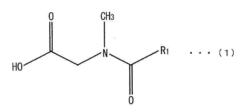
上記、一般式(1)中、R1は、炭素数10以上20以下の直鎖アルキル基又は炭素数10以上20以下の直鎖アルケニル基を示す。R1は、好ましくは、炭素数15以上20以下であり、より好ましくは炭素数が17である。また、R1は、直鎖アルキル基でもよく、炭素の二重結合を有する直鎖アルケニル基であってもよく、好ましくは直鎖アルケニル基である。
アミノ酸系分散剤は、導電性粉末100質量部に対して、好ましくは0.01質量部以上2質量部以下含有され、より好ましくは、0.05質量部以上1.5質量部以下含有され、さらに好ましくは0.05質量部以上1.0質量部以下含有される。アミノ酸系分散剤の含有量が上記範囲である場合、導電性ペースト中の導電性粉末の分散性に優れる。また、アミノ酸系分散剤は、上記範囲内で含有量を多くすることにより、導電性ペーストの粘度を低下させ、印刷性を向上させる傾向があるが、導電性ペーストの乾燥性が低下し、シートアタックが生じやすくなったり、印刷形状が維持できなくなったりするなどの傾向もある。このため、実使用に当たっては、導電性ペーストを用いる電子部品の要求に応じて、適切なバランスの組合せになる含有量の組成を選択すれば良い。
アミノ酸系分散剤は、導電性ペースト全体に対して、例えば、3質量%以下含有される。アミノ酸系分散剤の含有量の上限は、好ましく2質量%以下であり、より好ましくは1.5質量%以下であり、さらに好ましくは1質量%以下である。アミノ酸系分散剤の含有量の下限は、特に限定されないが、例えば、0.01質量%以上であり、好ましくは0.05質量%以上である。
有機溶剤の中には、バインダー樹脂と組み合わせて用いたとき、シートアタックやグリーンシート剥離不良を生じさせるものもあるが、アミノ酸系分散剤を特定量含有することで、これらの問題の発生を抑制できる。また、バインダー樹脂にアセタール系樹脂を含み、有機溶剤にグリコールエーテル系溶媒を含む導電性ペーストに、アミノ酸系分散剤を用いずに、他の酸系分散剤であるリン酸系分散剤などを用いる場合、塊状物が発生することがあるが、本実施形態の導電性ペーストを用いた場合、塊状物の発生を非常に抑制することができる。
アミノ酸系分散剤は、例えば、市販の製品から、上記特性を満たすものを選択して用いることができる。また、アミノ酸系分散剤は、従来公知の製造方法を用いて、上記特性を満たすように製造してもよい。
導電性ペーストは、アミノ酸系分散剤以外の他の酸系分散剤を含んでもよい。他の酸系分散剤としては、例えば、高級脂肪酸、高分子界面活性剤などが挙げられる。これらの分散剤は、1種または2種以上組み合わせて用いてもよい。
高級脂肪酸としては、不飽和カルボン酸でも飽和カルボン酸でもよく、特に限定されるものではないが、ステアリン酸、オレイン酸、ベヘン酸、ミリスチン酸、パルミチン酸、リノール酸、ラウリン酸、リノレン酸など炭素数11以上のものが挙げられる。中でも、オレイン酸、またはステアリン酸が好ましい。
それ以外の酸系分散剤としては、特に限定されず、モノアルキルアミン塩に代表されるアルキルモノアミン塩型、N−アルキル(C14~C18)プロピレンジアミンジオレイン酸塩に代表されるアルキルジアミン塩型、アルキルトリメチルアンモニウムクロライドに代表されるアルキルトリメチルアンモニウム塩型、ヤシアルキルジメチルベンジルアンモニウムクロライドに代表されるアルキルジメチルベンジルアンモニウム塩型、アルキル・ジポリオキシエチレンメチルアンモニウムクロライドに代表される4級アンモニウム塩型、アルキルピリジニウム塩型、ジメチルステアリルアミンに代表される3級アミン型、ポリオキシプロピレン・ポリオキシエチレンアルキルアミンに代表されるポリオキシエチレンアルキルアミン型、N、N’、N’−トリス(2−ヒドロキシエチル)−N−アルキル(C14~18)1,3−ジアミノプロパンに代表されるジアミンのオキシエチレン付加型から選択される界面活性剤が挙げられる。
また、分散剤は、酸系分散剤以外の分散剤を含んでもよい。酸系分散剤以外の分散剤としては、塩基系分散剤、非イオン系分散剤、両性分散剤などが挙げられる。これらの分散剤は、1種または2種以上組み合わせて用いてもよい。
塩基系分散剤としては、例えば、ラウリルアミン、ポリエチレングリコールラウリルアミン、ロジンアミン、セチルアミン、ミリスチルアミン、ステアリルアミン、オレイルアミンなどの脂肪族アミンなどが挙げられる。導電性ペーストは、アミノ酸系分散剤と合わせて、さらに塩基系分散とを含有する場合、経時的な粘度安定性と、ペースト分散性とを非常に高いレベルで両立させることができる。
塩基系分散剤は、例えば、導電性粉末100質量部に対して、0.01質量部以上2質量部未満含有されてもよく、好ましくは0.02質量部以上1質量部以下含有されてもよい。また、塩基系分散剤は、例えば、アミノ酸系分散剤100質量部に対して、10質量部以上300質量部以下程度含有されることができる。
また、導電性ペーストにおいて、塩基系分散剤の含有量は、アミノ酸系分散剤の含有量よりも少なくてもよく、アミノ酸系分散100質量部に対して、80質量部以下であってもよく、50質量部以下であってもよく、30質量部以下であってもよい。上述したバインダー樹脂、有機溶剤及びアミノ酸系分散剤と併せて、塩基系分散剤を上記範囲で含む場合、導電性ペーストの粘度をより低くすることができる。
また、導電性ペーストにおいて、塩基系分散剤の含有量は、アミノ酸系分散剤の含有量よりも少なくてもよく、アミノ酸系分散100質量部に対して、80質量部以下であってもよく、50質量部以下であってもよく、30質量部以下であってもよい。上述したバインダー樹脂、有機溶剤及びアミノ酸系分散剤と併せて、塩基系分散剤を上記範囲で含む場合、導電性ペーストの粘度をより低くすることができる。
塩基系分散剤は、例えば、導電性ペースト全体に対して、0質量%以上2.5質量%以下含有され、好ましくは0質量%以上1.0質量%以下、より好ましくは0.1質量%以上1.0質量%以下含有され、より好ましくは0.1質量%以上0.8質量%以下含有される。また、塩基系分散剤は、導電性ペースト全体に対して、0.3質量%以下であってもよい。塩基系分散を上記範囲で含有する場合、ペーストの経時的な粘度安定性により優れる。
導電性ペーストにおいて、アミノ酸系分散剤を含む分散剤(全体)の含有量は、例えば、導電性粉末100質量部に対して、好ましくは0.2質量部以上2質量部以下であり、1質量部以下であってもよい。分散剤(全体)の含有量が上記範囲を超える場合、導電性ペーストの乾燥性が悪化したり、シートアタックが生じたり、グリーンシートを台紙のPETフィルムから剥離できなくなる場合がある。
(その他の成分)
本実施形態の導電性ペーストは、必要に応じて、上記の成分以外のその他の成分を含んでもよい。その他の成分としては、例えば、消泡剤、可塑剤、界面活性剤、増粘剤などの従来公知の添加物を用いることができる。
本実施形態の導電性ペーストは、必要に応じて、上記の成分以外のその他の成分を含んでもよい。その他の成分としては、例えば、消泡剤、可塑剤、界面活性剤、増粘剤などの従来公知の添加物を用いることができる。
(導電性ペースト)
本実施形態の導電性ペーストの製造方法は、特に限定されず、従来公知の方法を用いることができる。導電性ペーストは、例えば、上記の各成分を、3本ロールミル、ボールミル、ミキサーなどで攪拌・混練することにより製造することができる。その際、導電性粉末表面に予め分散剤を塗布すると、導電性粉末が凝集することなく十分にほぐれて、その表面に分散剤が行きわたるようになり、均一な導電性ペーストを得やすい。また、予め、バインダー樹脂を有機溶剤の一部に溶解させて、有機ビヒクルを作製した後、ペースト調整用の有機溶剤へ、導電性粉末、セラミック粉末、分散剤、及び、有機ビヒクルを添加した後、攪拌・混練し、導電性ペーストを作製してもよい。
本実施形態の導電性ペーストの製造方法は、特に限定されず、従来公知の方法を用いることができる。導電性ペーストは、例えば、上記の各成分を、3本ロールミル、ボールミル、ミキサーなどで攪拌・混練することにより製造することができる。その際、導電性粉末表面に予め分散剤を塗布すると、導電性粉末が凝集することなく十分にほぐれて、その表面に分散剤が行きわたるようになり、均一な導電性ペーストを得やすい。また、予め、バインダー樹脂を有機溶剤の一部に溶解させて、有機ビヒクルを作製した後、ペースト調整用の有機溶剤へ、導電性粉末、セラミック粉末、分散剤、及び、有機ビヒクルを添加した後、攪拌・混練し、導電性ペーストを作製してもよい。
導電性ペーストは、ずり速度100sec−1の粘度が、好ましくは0.8Pa・S以下である。ずり速度100sec−1の粘度が上記範囲である場合、グラビア印刷用の導電性ペーストとして好適に用いることができる。上記範囲を超えると粘度が高すぎてグラビア印刷用として適さない場合がある。ずり速度100sec−1の粘度の下限は、特に限定されないが、例えば、0.2Pa・S以上である。
また、導電性ペーストは、ずり速度10000sec−1の粘度が、好ましくは0.18Pa・S以下である。ずり速度10000sec−1の粘度が上記範囲である場合、グラビア印刷用の導電性ペーストとして好適に用いることができる。上記範囲を超えた場合も、粘度が高すぎてグラビア印刷用として適さない場合がある。ずり速度10000sec−1の粘度の下限は、特に限定されないが、例えば、0.05Pa・S以上である。
導電性ペーストは、積層セラミックコンデンサなどの電子部品に好適に用いることができる。積層セラミックコンデンサは、誘電体グリーンシートを用いて形成される誘電体層及び導電性ペーストを用いて形成される内部電極層を有する。
積層セラミックコンデンサは、誘電体グリーンシートに含まれる誘電体セラミック粉末と導電性ペーストに含まれるセラミック粉末とが同一組成の粉末であることが好ましい。本実施形態の導電性ペーストを用いて製造される積層セラミックデバイスは、誘電体グリーンシートの厚さが、例えば3μm以下である場合でも、シートアタックやグリーンシートの剥離不良が抑制される。
[電子部品]
以下、本発明の電子部品等の実施形態について、図面を参照しながら説明する。図面においては、適宜、模式的に表現することや、縮尺を変更して表現することがある。また、部材の位置や方向などを、適宜、図1などに示すXYZ直交座標系を参照して説明する。このXYZ直交座標系において、X方向およびY方向は水平方向であり、Z方向は鉛直方向(上下方向)である。
以下、本発明の電子部品等の実施形態について、図面を参照しながら説明する。図面においては、適宜、模式的に表現することや、縮尺を変更して表現することがある。また、部材の位置や方向などを、適宜、図1などに示すXYZ直交座標系を参照して説明する。このXYZ直交座標系において、X方向およびY方向は水平方向であり、Z方向は鉛直方向(上下方向)である。
図1A及びBは、実施形態に係る電子部品の一例である、積層セラミックコンデンサ1を示す図である。積層セラミックコンデンサ1は、誘電体層12及び内部電極層11を交互に積層した積層体10と外部電極20とを備える。
以下、上記導電性ペーストを使用した積層セラミックコンデンサの製造方法について説明する。まず、誘電体グリーンシート上に、導電性ペーストを印刷して、乾燥し乾燥膜を形成し、この乾燥膜を上面に有する複数の誘電体グリーンシートを、圧着により積層させた後、焼成して一体化することにより、セラミックコンデンサ本体となる積層セラミック焼成体(積層体10)を作製する。その後、積層体10の両端部に一対の外部電極20を形成することにより積層セラミックコンデンサ1が製造される。以下に、より詳細に説明する。
まず、未焼成のセラミックシートである誘電体グリーンシート(セラミックグリーンシート)を用意する。この誘電体グリーンシートとしては、例えば、チタン酸バリウム等の所定のセラミックの原料粉末に、ポリビニルブチラール等の有機バインダーとターピネオール等の溶剤とを加えて得た誘電体層用ペーストを、PETフィルム等の支持フィルム上にシート状に塗布し、乾燥させて溶剤を除去したもの等が挙げられる。なお、誘電体グリーンシートからなる誘電体層の厚みは、特に限定されないが、積層セラミックコンデンサ1の小型化の要請の観点から、0.05μm以上3μm以下が好ましい。
次いで、この誘電体グリーンシートの片面に、グラビア印刷法を用いて、上述の導電性ペーストを印刷して塗布し、乾燥させて乾燥膜を形成したものを複数枚、用意する。なお、印刷後の導電性ペースト(乾燥膜)の厚みは、内部電極層11の薄層化の要請の観点から、乾燥後1μm以下とすることが好ましい。
次いで、支持フィルムから、誘電体グリーンシートを剥離するとともに、誘電体グリーンシートとその片面に形成された導電性ペースト(乾燥膜)とが交互に配置されるように積層した後、加熱・加圧処理により積層体(圧着体)を得る。なお、積層体の両面に、導電性ペーストを塗布していない保護用の誘電体グリーンシートを更に配置する構成としても良い。
次いで、積層体を所定サイズに切断してグリーンチップを形成した後、当該グリーンチップに対して脱バインダー処理を施し、還元雰囲気下において焼成することにより、積層セラミック焼成体(積層体10)を製造する。なお、脱バインダー処理における雰囲気は、大気またはN2ガス雰囲気にすることが好ましい。脱バインダー処理を行う際の温度は、例えば200℃以上400℃以下である。また、脱バインダー処理を行う際の、上記温度の保持時間を0.5時間以上24時間以下とすることが好ましい。また、焼成は、内部電極層11に用いる金属の酸化を抑制するために還元雰囲気で行われ、また、積層体10の焼成を行う際の温度は、例えば、1000℃以上1350℃以下であり、焼成を行う際の、温度の保持時間は、例えば、0.5時間以上8時間以下である。
グリーンチップの焼成を行うことにより、誘電体グリーンシート中の有機バインダーが完全に除去されるとともに、セラミックの原料粉末が焼成されて、セラミック製の誘電体層12が形成される。また乾燥膜中の有機ビヒクルが除去されるとともに、ニッケル粉末またはニッケルを主成分とする合金粉末が焼結もしくは溶融、一体化されて、内部電極層11が形成され、誘電体層12と内部電極層11とが複数枚、交互に積層された積層セラミック焼成体(積層体10)が形成される。なお、酸素を誘電体層12の内部に取り込んで信頼性を高めるとともに、内部電極層11の再酸化を抑制するとの観点から、焼成後の積層セラミック焼成体(積層体10)に対して、アニール処理を施してもよい。
そして、作製した積層セラミック焼成体(積層体10)に対して、一対の外部電極20を設けることにより、積層セラミックコンデンサ1が製造される。例えば、外部電極20は、外部電極層21及びメッキ層22を備える。外部電極層21は、内部電極層11と電気的に接続する。なお、外部電極20の材料としては、例えば、銅やニッケル、またはこれらの合金が好適に使用できる。なお、電子部品は、積層セラミックコンデンサ以外の電子部品を用いることもできる。
以下、本発明を実施例と比較例に基づき詳細に説明するが、本発明は実施例によって何ら限定されるものではない。
[評価方法]
(導電性ペーストの粘度)
導電性ペーストの製造後の粘度を、レオメーターを用いて、ずり速度100sec−1、10000sec−1の条件で測定した。
(導電性ペーストの粘度)
導電性ペーストの製造後の粘度を、レオメーターを用いて、ずり速度100sec−1、10000sec−1の条件で測定した。
(導電性ペーストの分散性)
導電性ペーストの分散性を下記の方法により評価した。
ガラス基板(2inch)上に、サンプルを印刷し(GAP厚=5μm)乾燥する。乾燥は、ベルト炉内の最大温度120~150℃、大気雰囲気にて行った。乾燥後に得られた乾燥膜(2cm×2cm、厚さ3μm)を、光学顕微鏡を用いて、ガラス基板の裏面から光(バックライト)を当てながら、×100(接眼、対物;各10倍)で観察して、塊状物の有無を確認した。塊状物が観察されない場合、導電性ペーストの分散性が良好であり、塊状物が1以上観察される場合を、導電性ペーストの分散性が不良であると判断できる。
導電性ペーストの分散性を下記の方法により評価した。
ガラス基板(2inch)上に、サンプルを印刷し(GAP厚=5μm)乾燥する。乾燥は、ベルト炉内の最大温度120~150℃、大気雰囲気にて行った。乾燥後に得られた乾燥膜(2cm×2cm、厚さ3μm)を、光学顕微鏡を用いて、ガラス基板の裏面から光(バックライト)を当てながら、×100(接眼、対物;各10倍)で観察して、塊状物の有無を確認した。塊状物が観察されない場合、導電性ペーストの分散性が良好であり、塊状物が1以上観察される場合を、導電性ペーストの分散性が不良であると判断できる。
[使用材料]
(導電性粉末)
導電性粉末としては、Ni粉末(平均粒径0.3μm)を使用した。
(導電性粉末)
導電性粉末としては、Ni粉末(平均粒径0.3μm)を使用した。
(セラミック粉末)
セラミック粉末としては、チタン酸バリウム(BaTiO3;平均粒径0.06μm)を使用した。
セラミック粉末としては、チタン酸バリウム(BaTiO3;平均粒径0.06μm)を使用した。
(バインダー樹脂)
バインダー樹脂としては、ポリビニルブチラール樹脂(PVB)、エチルセルロース(EC)を使用した。
バインダー樹脂としては、ポリビニルブチラール樹脂(PVB)、エチルセルロース(EC)を使用した。
(分散剤)
(1)分子量5000以下のアミノ酸系分散剤として、上記一般式(1)中、R1=C17H33で示される酸系分散剤(A)、R1=C11H23で示される酸系分散剤(B)を用いた。
(1)分子量5000以下のアミノ酸系分散剤として、上記一般式(1)中、R1=C17H33で示される酸系分散剤(A)、R1=C11H23で示される酸系分散剤(B)を用いた。

(2)塩基系分散剤として、ロジンアミン(C)、ポリエチレングリコールラウリルアミン(D)、オレイルアミン(E)を用いた。
(3)リン酸系分散剤として、リン酸ポリエステル(F)を用いた。
(3)リン酸系分散剤として、リン酸ポリエステル(F)を用いた。
(有機溶剤)
有機溶剤としては、プロピレングリコールモノブチルエーテル(PNB)、ミネラルスピリット(MA)、ターピネオール(TPO)を使用した。
有機溶剤としては、プロピレングリコールモノブチルエーテル(PNB)、ミネラルスピリット(MA)、ターピネオール(TPO)を使用した。
[実施例1]
導電性粉末であるNi粉末100質量部に対して、セラミック粉末25質量部と、分散剤としてアミノ酸系分散剤(A)2質量部と、バインダー樹脂として、PVB2質量部およびEC4質量部と、有機溶剤としてPNB41質量部およびMA27質量部と、を混合して導電性ペーストを作製した。作製した導電性ペーストの粘度及びペーストの分散性を上記方法で評価した。導電性ペーストの分散剤等の含有量を表1に、導電性ペーストの粘度、及び、分散性の評価結果を表2に示す。
導電性粉末であるNi粉末100質量部に対して、セラミック粉末25質量部と、分散剤としてアミノ酸系分散剤(A)2質量部と、バインダー樹脂として、PVB2質量部およびEC4質量部と、有機溶剤としてPNB41質量部およびMA27質量部と、を混合して導電性ペーストを作製した。作製した導電性ペーストの粘度及びペーストの分散性を上記方法で評価した。導電性ペーストの分散剤等の含有量を表1に、導電性ペーストの粘度、及び、分散性の評価結果を表2に示す。
[実施例2]
分散剤として、アミノ酸系分散剤(A)1.5質量部を用いた以外は、実施例1と同様に導電性ペーストを作製して、評価した。導電性ペーストの分散剤等の含有量を表1に、導電性ペーストの粘度、及び、分散性の評価結果を表2に示す。
分散剤として、アミノ酸系分散剤(A)1.5質量部を用いた以外は、実施例1と同様に導電性ペーストを作製して、評価した。導電性ペーストの分散剤等の含有量を表1に、導電性ペーストの粘度、及び、分散性の評価結果を表2に示す。
[実施例3]
分散剤として、アミノ酸系分散剤(A)0.8質量部を用いた以外は、実施例1と同様に導電性ペーストを作製して、評価した。導電性ペーストの分散剤等の含有量を表1に、導電性ペーストの粘度、及び、分散性の評価結果を表2に示す。
分散剤として、アミノ酸系分散剤(A)0.8質量部を用いた以外は、実施例1と同様に導電性ペーストを作製して、評価した。導電性ペーストの分散剤等の含有量を表1に、導電性ペーストの粘度、及び、分散性の評価結果を表2に示す。
[実施例4]
分散剤として、アミノ酸系分散剤(A)0.05質量部を用いた以外は、実施例1と同様に導電性ペーストを作製して、評価した。導電性ペーストの分散剤等の含有量を表1に、導電性ペーストの粘度、及び、分散性の評価結果を表2に示す。
分散剤として、アミノ酸系分散剤(A)0.05質量部を用いた以外は、実施例1と同様に導電性ペーストを作製して、評価した。導電性ペーストの分散剤等の含有量を表1に、導電性ペーストの粘度、及び、分散性の評価結果を表2に示す。
[実施例5]
分散剤として、アミノ酸系分散剤(A)0.01質量部を用いた以外は、実施例1と同様に導電性ペーストを作製して、評価した。導電性ペーストの分散剤等の含有量を表1に、導電性ペーストの粘度、及び、分散性の評価結果を表2に示す。
分散剤として、アミノ酸系分散剤(A)0.01質量部を用いた以外は、実施例1と同様に導電性ペーストを作製して、評価した。導電性ペーストの分散剤等の含有量を表1に、導電性ペーストの粘度、及び、分散性の評価結果を表2に示す。
[実施例6]
分散剤として、アミノ酸系分散剤(A)0.8質量部およびロジンアミン(C)0.2質量部を用いた以外は、実施例1と同様に導電性ペーストを作製して、評価した。導電性ペーストの分散剤等の含有量を表1に、導電性ペーストの粘度、及び、分散性の評価結果を表2に示す。
分散剤として、アミノ酸系分散剤(A)0.8質量部およびロジンアミン(C)0.2質量部を用いた以外は、実施例1と同様に導電性ペーストを作製して、評価した。導電性ペーストの分散剤等の含有量を表1に、導電性ペーストの粘度、及び、分散性の評価結果を表2に示す。
[実施例7]
分散剤として、アミノ酸系分散剤(A)0.8質量部およびポリエチレングリコールラウリルアミン(D)0.2質量部を用いた以外は、実施例1と同様に導電性ペーストを作製して、評価した。導電性ペーストの分散剤等の含有量を表1に、導電性ペーストの粘度、及び、分散性の評価結果を表2に示す。
分散剤として、アミノ酸系分散剤(A)0.8質量部およびポリエチレングリコールラウリルアミン(D)0.2質量部を用いた以外は、実施例1と同様に導電性ペーストを作製して、評価した。導電性ペーストの分散剤等の含有量を表1に、導電性ペーストの粘度、及び、分散性の評価結果を表2に示す。
[実施例8]
分散剤として、アミノ酸系分散剤(A)0.8質量部およびオレイルアミン(E)0.2質量部を用いた以外は、実施例1と同様に導電性ペーストを作製して、評価した。導電性ペーストの分散剤等の含有量を表1に、導電性ペーストの粘度、及び、分散性の評価結果を表2に示す。
分散剤として、アミノ酸系分散剤(A)0.8質量部およびオレイルアミン(E)0.2質量部を用いた以外は、実施例1と同様に導電性ペーストを作製して、評価した。導電性ペーストの分散剤等の含有量を表1に、導電性ペーストの粘度、及び、分散性の評価結果を表2に示す。
[実施例9]
バインダー樹脂として、PVB6質量部のみを用いた以外は、実施例3と同様に導電性ペーストを作製して、評価した。導電性ペーストの分散剤等の含有量を表1に、導電性ペーストの粘度、及び、分散性の評価結果を表2に示す。
バインダー樹脂として、PVB6質量部のみを用いた以外は、実施例3と同様に導電性ペーストを作製して、評価した。導電性ペーストの分散剤等の含有量を表1に、導電性ペーストの粘度、及び、分散性の評価結果を表2に示す。
[実施例10]
有機溶剤としてPNB50質量部およびMA18質量部を用いた以外は、実施例3と同様に導電性ペーストを作製して、評価した。導電性ペーストの分散剤等の含有量を表1に、導電性ペーストの粘度、及び、分散性の評価結果を表2に示す。
有機溶剤としてPNB50質量部およびMA18質量部を用いた以外は、実施例3と同様に導電性ペーストを作製して、評価した。導電性ペーストの分散剤等の含有量を表1に、導電性ペーストの粘度、及び、分散性の評価結果を表2に示す。
[実施例11]
分散剤として、アミノ酸系分散剤(B)0.8質量部を用いた以外は、実施例1と同様に導電性ペーストを作製して、評価した。導電性ペーストの分散剤等の含有量を表1に、導電性ペーストの粘度、及び、分散性の評価結果を表2に示す。
分散剤として、アミノ酸系分散剤(B)0.8質量部を用いた以外は、実施例1と同様に導電性ペーストを作製して、評価した。導電性ペーストの分散剤等の含有量を表1に、導電性ペーストの粘度、及び、分散性の評価結果を表2に示す。
[実施例12]
分散剤として、アミノ酸系分散剤(B)0.8質量部およびロジンアミン(C)0.2質量部を用いた以外は、実施例1と同様に導電性ペーストを作製して、評価した。導電性ペーストの分散剤等の含有量を表1に、導電性ペーストの粘度、及び、分散性の評価結果を表2に示す。
分散剤として、アミノ酸系分散剤(B)0.8質量部およびロジンアミン(C)0.2質量部を用いた以外は、実施例1と同様に導電性ペーストを作製して、評価した。導電性ペーストの分散剤等の含有量を表1に、導電性ペーストの粘度、及び、分散性の評価結果を表2に示す。
[比較例1]
分散剤として、リン酸系分散剤(F)0.8質量部を用いた以外は、実施例1と同様に導電性ペーストを作製して、評価した。導電性ペーストの分散剤等の含有量を表1に、導電性ペーストの粘度、及び、分散性の評価結果を表2に示す。
分散剤として、リン酸系分散剤(F)0.8質量部を用いた以外は、実施例1と同様に導電性ペーストを作製して、評価した。導電性ペーストの分散剤等の含有量を表1に、導電性ペーストの粘度、及び、分散性の評価結果を表2に示す。
[比較例2]
分散剤として、リン酸系分散剤(F)0.8質量部及び塩基系分散剤(C)0.2質量部を用いた以外は、実施例1と同様に導電性ペーストを作製して、評価した。導電性ペーストの分散剤等の含有量を表1に、導電性ペーストの粘度、及び、分散性の評価結果を表2に示す。
分散剤として、リン酸系分散剤(F)0.8質量部及び塩基系分散剤(C)0.2質量部を用いた以外は、実施例1と同様に導電性ペーストを作製して、評価した。導電性ペーストの分散剤等の含有量を表1に、導電性ペーストの粘度、及び、分散性の評価結果を表2に示す。
[比較例3]
分散剤として、塩基系分散剤(C)0.8質量部のみを用いた以外は、実施例1と同様に導電性ペーストを作製して、評価した。導電性ペーストの分散剤等の含有量を表1に、導電性ペーストの粘度、及び、分散性の評価結果を表2に示す。
分散剤として、塩基系分散剤(C)0.8質量部のみを用いた以外は、実施例1と同様に導電性ペーストを作製して、評価した。導電性ペーストの分散剤等の含有量を表1に、導電性ペーストの粘度、及び、分散性の評価結果を表2に示す。
[比較例4]
有機溶剤としてターピネオール(TPO)のみを用いた以外は、実施例3と同様に導電性ペーストを作製して、評価した。導電性ペーストの分散剤等の含有量を表1に、導電性ペーストの粘度、及び、分散性の評価結果を表2に示す。
[比較例5]
バインダー樹脂としてECのみを用いた以外は、実施例3と同様に導電性ペーストを作製して、評価した。導電性ペーストの分散剤等の含有量を表1に、導電性ペーストの粘度、及び、分散性の評価結果を表2に示す。
[比較例6]
バインダー樹脂としてECのみ、及び、有機溶剤としてターピネオール(TPO)のみを用いた以外は、実施例3と同様に導電性ペーストを作製して、評価した。導電性ペーストの分散剤等の含有量を表1に、導電性ペーストの粘度、及び、分散性の評価結果を表2に示す。


(評価結果)
実施例の導電性ペーストは、ずり速度100sec−1の粘度が0.44~0.79Pa・Sであり、ずり速度10000sec−1の粘度が0.13~0.18Pa・Sであり、グラビア印刷に適した粘度であった。また、本実施例の導電性ペーストは、印刷後の乾燥膜表面に塊状物が観察されず、ペーストの分散性に優れることが示された。
実施例の導電性ペーストは、ずり速度100sec−1の粘度が0.44~0.79Pa・Sであり、ずり速度10000sec−1の粘度が0.13~0.18Pa・Sであり、グラビア印刷に適した粘度であった。また、本実施例の導電性ペーストは、印刷後の乾燥膜表面に塊状物が観察されず、ペーストの分散性に優れることが示された。
一方、アミノ酸系分散剤の代わりにリン酸系分散剤を含む比較例1および2の導電性ペーストでは、印刷後の乾燥膜表面に塊状物が観察され、ペーストの分散性が不良であることが示された。また、分散剤が酸系分散剤を含まず塩基系分散剤のみからなる比較例3、有機溶剤が本発明の範囲から外れる比較例4、バインダー樹脂が本発明の範囲から外れる比較例5、および、有機溶剤とバインダー樹脂とが本発明の範囲から外れる比較例6の導電性ペーストでは、グラビア印刷に適した粘度を得ることができなかった。そのため、印刷後の表面性状が荒れてしまい、十分平滑にならなかったため塊状物の観察は行わなかった。
本発明の導電性ペーストは、グラビア印刷に適した粘度を有し、かつ、ペーストの分散性が良好である。よって、本発明の導電性ペーストは、特に携帯電話やデジタル機器などの電子機器のチップ部品である積層セラミックコンデンサの内部電極用の原料として好適に用いることができ、特に、グラビア印刷用の導電性ペーストとして好適に用いることができる。
1 積層セラミックコンデンサ
10 積層体
11 内部電極層
12 誘電体層
20 外部電極
21 外部電極層
22 メッキ層
10 積層体
11 内部電極層
12 誘電体層
20 外部電極
21 外部電極層
22 メッキ層
Claims (15)
- 導電性粉末、分散剤、バインダー樹脂及び有機溶剤を含む導電性ペーストであって、
前記分散剤は、分子量が5000以下のアミノ酸系分散剤を含み、
前記バインダー樹脂は、アセタール系樹脂を含み、
前記有機溶剤は、グリコールエーテル系溶剤を含む、
導電性ペースト。 - 前記アミノ酸系分散剤は、下記の一般式(1)で示される、請求項1に記載の導電性ペースト。
- 前記アミノ酸系分散剤は、前記導電性粉末100質量部に対して0.01質量部以上2質量部以下含有される、請求項1又は2に記載の導電性ペースト。
- 前記グリコールエーテル系溶剤は、前記導電性粉末100質量部に対して30質量部以上50質量部以下含有される、請求項1~3のいずれか一項に記載の導電性ペースト。
- 前記分散剤は、さらに塩基系分散剤を含む、請求項1~4のいずれか一項に記載の導電性ペースト。
- 前記分散剤は、前記導電性粉末100質量部に対して、0.01質量部以上2質量部以下含有される、請求項1~5のいずれか一項に記載の導電性ペースト。
- 前記導電性粉末は、Ni、Pd、Pt、Au、Ag、Cu及びこれらの合金から選ばれる少なくとも1種の金属粉末を含む、請求項1~6のいずれか一項に記載の導電性ペースト。
- 前記導電性粉末は、平均粒径が0.05μm以上1.0μm以下である、請求項1~7のいずれか一項に記載の導電性ペースト。
- セラミック粉末を含む、請求項1~8のいずれか一項に記載の導電性ペースト。
- 前記セラミック粉末は、ペロブスカイト型酸化物を含む、請求項9に記載の導電性ペースト。
- 前記セラミック粉末は、平均粒径が0.01μm以上0.5μm以下である、請求項9又は10に記載の導電性ペースト。
- 積層セラミック部品の内部電極用である、請求項1~11のいずれか一項に記載の導電性ペースト。
- ずり速度100sec−1での粘度が0.8Pa・S以下であり、ずり速度10000sec−1での粘度が0.18Pa・S以下である、請求項1~12のいずれか一項に記載の導電性ペースト。
- 請求項1~13のいずれか一項に記載の導電性ペーストを用いて形成される電子部品。
- 誘電体層と内部電極とを積層した積層体を少なくとも有し、
前記内部電極は、請求項1~13のいずれか一項に記載の導電性ペーストを用いて形成される積層セラミックコンデンサ。
Priority Applications (2)
| Application Number | Priority Date | Filing Date | Title |
|---|---|---|---|
| KR1020207005892A KR20200116445A (ko) | 2017-08-30 | 2018-10-30 | 도전성 페이스트, 전자 부품 및 적층 세라믹 콘덴서 |
| CN201880056646.8A CN111052263B (zh) | 2017-08-30 | 2018-10-30 | 导电性浆料、电子部件以及叠层陶瓷电容器 |
Applications Claiming Priority (4)
| Application Number | Priority Date | Filing Date | Title |
|---|---|---|---|
| JP2017165894 | 2017-08-30 | ||
| JP2017-165894 | 2017-08-30 | ||
| JP2018035050A JP2019046781A (ja) | 2017-08-30 | 2018-02-28 | 導電性ペースト、並びに、電子部品及び積層セラミックコンデンサの製造方法 |
| JP2018-035050 | 2018-02-28 |
Publications (2)
| Publication Number | Publication Date |
|---|---|
| WO2019043672A2 true WO2019043672A2 (ja) | 2019-03-07 |
| WO2019043672A3 WO2019043672A3 (ja) | 2019-05-02 |
Family
ID=65525065
Family Applications (1)
| Application Number | Title | Priority Date | Filing Date |
|---|---|---|---|
| PCT/IB2018/058471 WO2019043672A2 (ja) | 2017-08-30 | 2018-10-30 | 導電性ペースト、電子部品及び積層セラミックコンデンサ |
Country Status (1)
| Country | Link |
|---|---|
| WO (1) | WO2019043672A2 (ja) |
Family Cites Families (6)
| Publication number | Priority date | Publication date | Assignee | Title |
|---|---|---|---|---|
| JP4439897B2 (ja) * | 2003-12-04 | 2010-03-24 | 旭化成ケミカルズ株式会社 | 導電性組成物 |
| JP4947509B2 (ja) * | 2004-12-09 | 2012-06-06 | 三井金属鉱業株式会社 | ニッケルスラリー及びその製造方法並びに該ニッケルスラリーを用いたニッケルペースト又はニッケルインキ |
| JP5569747B2 (ja) * | 2011-02-18 | 2014-08-13 | 住友金属鉱山株式会社 | 積層セラミックコンデンサ内部電極に用いられるグラビア印刷用導電性ペースト |
| KR20130125944A (ko) * | 2012-05-10 | 2013-11-20 | 삼성전기주식회사 | 내부 전극용 도전성 페이스트 조성물, 적층 세라믹 전자부품 및 이의 제조방법 |
| JP6314728B2 (ja) * | 2014-07-30 | 2018-04-25 | 住友金属鉱山株式会社 | 導電性ペーストの製造方法及びこれにより得られる導電性ペースト |
| KR102410080B1 (ko) * | 2014-07-31 | 2022-06-16 | 스미토모 긴조쿠 고잔 가부시키가이샤 | 도전성 페이스트 |
-
2018
- 2018-10-30 WO PCT/IB2018/058471 patent/WO2019043672A2/ja active Application Filing
Also Published As
| Publication number | Publication date |
|---|---|
| WO2019043672A3 (ja) | 2019-05-02 |
Similar Documents
| Publication | Publication Date | Title |
|---|---|---|
| WO2017150438A1 (ja) | 導電性ペースト、電子部品及び積層セラミックコンデンサ | |
| WO2019107501A1 (ja) | 導電性ペースト、電子部品、及び積層セラミックコンデンサ | |
| TWI801445B (zh) | 導電性漿料、電子零件以及層積陶瓷電容器 | |
| JP7405098B2 (ja) | 導電性ペースト、電子部品、及び積層セラミックコンデンサ | |
| JP2024032861A (ja) | 導電性ペースト、電子部品、及び積層セラミックコンデンサ | |
| WO2019107500A1 (ja) | 導電性ペースト、電子部品、及び積層セラミックコンデンサ | |
| CN111066098B (zh) | 导电性浆料、电子部件以及叠层陶瓷电容器 | |
| CN111386579B (zh) | 导电性浆料、电子部件以及叠层陶瓷电容器 | |
| JP2019046782A (ja) | 導電性ペースト、並びに、電子部品及び積層セラミックコンデンサの製造方法 | |
| WO2019043674A2 (ja) | 導電性ペースト、電子部品、及び積層セラミックコンデンサ | |
| WO2019043672A2 (ja) | 導電性ペースト、電子部品及び積層セラミックコンデンサ | |
| WO2019043673A2 (ja) | 導電性ペースト、電子部品、及び積層セラミックコンデンサ |
Legal Events
| Date | Code | Title | Description |
|---|---|---|---|
| 121 | Ep: the epo has been informed by wipo that ep was designated in this application |
Ref document number: 18851913 Country of ref document: EP Kind code of ref document: A2 |
|
| NENP | Non-entry into the national phase |
Ref country code: DE |
|
| 122 | Ep: pct application non-entry in european phase |
Ref document number: 18851913 Country of ref document: EP Kind code of ref document: A2 |