WO2020116165A1 - 半導体レーザ装置 - Google Patents
半導体レーザ装置 Download PDFInfo
- Publication number
- WO2020116165A1 WO2020116165A1 PCT/JP2019/045434 JP2019045434W WO2020116165A1 WO 2020116165 A1 WO2020116165 A1 WO 2020116165A1 JP 2019045434 W JP2019045434 W JP 2019045434W WO 2020116165 A1 WO2020116165 A1 WO 2020116165A1
- Authority
- WO
- WIPO (PCT)
- Prior art keywords
- semiconductor laser
- main surface
- laser device
- back surface
- main
- Prior art date
- Legal status (The legal status is an assumption and is not a legal conclusion. Google has not performed a legal analysis and makes no representation as to the accuracy of the status listed.)
- Ceased
Links
Images




















Classifications
-
- H—ELECTRICITY
- H01—ELECTRIC ELEMENTS
- H01S—DEVICES USING THE PROCESS OF LIGHT AMPLIFICATION BY STIMULATED EMISSION OF RADIATION [LASER] TO AMPLIFY OR GENERATE LIGHT; DEVICES USING STIMULATED EMISSION OF ELECTROMAGNETIC RADIATION IN WAVE RANGES OTHER THAN OPTICAL
- H01S5/00—Semiconductor lasers
- H01S5/02—Structural details or components not essential to laser action
- H01S5/022—Mountings; Housings
- H01S5/0239—Combinations of electrical or optical elements
-
- H—ELECTRICITY
- H01—ELECTRIC ELEMENTS
- H01S—DEVICES USING THE PROCESS OF LIGHT AMPLIFICATION BY STIMULATED EMISSION OF RADIATION [LASER] TO AMPLIFY OR GENERATE LIGHT; DEVICES USING STIMULATED EMISSION OF ELECTROMAGNETIC RADIATION IN WAVE RANGES OTHER THAN OPTICAL
- H01S5/00—Semiconductor lasers
- H01S5/02—Structural details or components not essential to laser action
- H01S5/022—Mountings; Housings
- H01S5/0233—Mounting configuration of laser chips
- H01S5/02345—Wire-bonding
-
- H—ELECTRICITY
- H01—ELECTRIC ELEMENTS
- H01S—DEVICES USING THE PROCESS OF LIGHT AMPLIFICATION BY STIMULATED EMISSION OF RADIATION [LASER] TO AMPLIFY OR GENERATE LIGHT; DEVICES USING STIMULATED EMISSION OF ELECTROMAGNETIC RADIATION IN WAVE RANGES OTHER THAN OPTICAL
- H01S5/00—Semiconductor lasers
- H01S5/02—Structural details or components not essential to laser action
- H01S5/022—Mountings; Housings
- H01S5/023—Mount members, e.g. sub-mount members
- H01S5/02315—Support members, e.g. bases or carriers
-
- H—ELECTRICITY
- H01—ELECTRIC ELEMENTS
- H01S—DEVICES USING THE PROCESS OF LIGHT AMPLIFICATION BY STIMULATED EMISSION OF RADIATION [LASER] TO AMPLIFY OR GENERATE LIGHT; DEVICES USING STIMULATED EMISSION OF ELECTROMAGNETIC RADIATION IN WAVE RANGES OTHER THAN OPTICAL
- H01S5/00—Semiconductor lasers
- H01S5/04—Processes or apparatus for excitation, e.g. pumping, e.g. by electron beams
- H01S5/042—Electrical excitation ; Circuits therefor
-
- H—ELECTRICITY
- H01—ELECTRIC ELEMENTS
- H01S—DEVICES USING THE PROCESS OF LIGHT AMPLIFICATION BY STIMULATED EMISSION OF RADIATION [LASER] TO AMPLIFY OR GENERATE LIGHT; DEVICES USING STIMULATED EMISSION OF ELECTROMAGNETIC RADIATION IN WAVE RANGES OTHER THAN OPTICAL
- H01S5/00—Semiconductor lasers
- H01S5/04—Processes or apparatus for excitation, e.g. pumping, e.g. by electron beams
- H01S5/042—Electrical excitation ; Circuits therefor
- H01S5/0427—Electrical excitation ; Circuits therefor for applying modulation to the laser
-
- H—ELECTRICITY
- H01—ELECTRIC ELEMENTS
- H01S—DEVICES USING THE PROCESS OF LIGHT AMPLIFICATION BY STIMULATED EMISSION OF RADIATION [LASER] TO AMPLIFY OR GENERATE LIGHT; DEVICES USING STIMULATED EMISSION OF ELECTROMAGNETIC RADIATION IN WAVE RANGES OTHER THAN OPTICAL
- H01S5/00—Semiconductor lasers
- H01S5/06—Arrangements for controlling the laser output parameters, e.g. by operating on the active medium
- H01S5/0607—Arrangements for controlling the laser output parameters, e.g. by operating on the active medium by varying physical parameters other than the potential of the electrodes, e.g. by an electric or magnetic field, mechanical deformation, pressure, light, temperature
- H01S5/0608—Arrangements for controlling the laser output parameters, e.g. by operating on the active medium by varying physical parameters other than the potential of the electrodes, e.g. by an electric or magnetic field, mechanical deformation, pressure, light, temperature controlled by light, e.g. optical switch
-
- H—ELECTRICITY
- H01—ELECTRIC ELEMENTS
- H01S—DEVICES USING THE PROCESS OF LIGHT AMPLIFICATION BY STIMULATED EMISSION OF RADIATION [LASER] TO AMPLIFY OR GENERATE LIGHT; DEVICES USING STIMULATED EMISSION OF ELECTROMAGNETIC RADIATION IN WAVE RANGES OTHER THAN OPTICAL
- H01S5/00—Semiconductor lasers
- H01S5/02—Structural details or components not essential to laser action
- H01S5/022—Mountings; Housings
- H01S5/02208—Mountings; Housings characterised by the shape of the housings
-
- H—ELECTRICITY
- H01—ELECTRIC ELEMENTS
- H01S—DEVICES USING THE PROCESS OF LIGHT AMPLIFICATION BY STIMULATED EMISSION OF RADIATION [LASER] TO AMPLIFY OR GENERATE LIGHT; DEVICES USING STIMULATED EMISSION OF ELECTROMAGNETIC RADIATION IN WAVE RANGES OTHER THAN OPTICAL
- H01S5/00—Semiconductor lasers
- H01S5/02—Structural details or components not essential to laser action
- H01S5/022—Mountings; Housings
- H01S5/02218—Material of the housings; Filling of the housings
- H01S5/02234—Resin-filled housings; the housings being made of resin
Definitions
- the present disclosure relates to a semiconductor laser device.
- LiDAR Light Detection and Ranging, Laser Imaging and Detection and Ranging
- Patent Document 1 A semiconductor laser device used as a light source for LiDAR emits pulsed laser light having a pulse width of tens of nanoseconds or less. Therefore, the rate of change of the current with time increases, and the loss due to the inductance component in the semiconductor laser device increases.
- the present disclosure has been devised under the above circumstances, and an object thereof is to provide a semiconductor laser device capable of reducing an inductance component.
- a semiconductor laser device provided by the present disclosure has a semiconductor laser element, a switching element having a gate electrode, a source electrode, and a drain electrode, and a conductive portion forming a conduction path to the switching element and the semiconductor laser element.
- a semiconductor laser device comprising: the semiconductor laser element and a supporting member supporting the switching element, wherein the conductive portion has a first portion separated from the semiconductor laser element, and the source of the switching element.
- the semiconductor laser device of the present disclosure it is possible to reduce the inductance component.
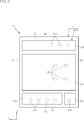
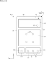
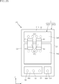
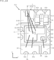
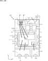
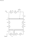
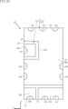
- FIG. 3 is a plan view of a main portion showing the semiconductor laser device according to the first embodiment of the present disclosure.
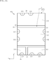
- FIG. 3 is a bottom view showing the semiconductor laser device according to the first embodiment of the present disclosure.
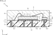
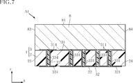
- FIG. 3 is a sectional view taken along the line III-III in FIG. 1.
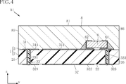
- FIG. 4 is a sectional view taken along the line IV-IV in FIG. 1.
- FIG. 5 is a sectional view taken along line VV of FIG. 1.
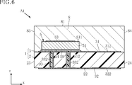
- FIG. 6 is a sectional view taken along line VI-VI in FIG. 1. It is sectional drawing which follows the VII-VII line of FIG.
- FIG. 1 is a circuit diagram showing a laser system including a semiconductor laser device according to a first embodiment of the present disclosure.
- FIG. 1 is a circuit diagram showing a laser system including a semiconductor laser device according to a first embodiment of the present disclosure.
- FIG. 8 is a circuit diagram showing a first modification of a laser system including the semiconductor laser device according to the first embodiment of the present disclosure.
- FIG. 8 is a circuit diagram showing a second modification of the laser system including the semiconductor laser device according to the first embodiment of the present disclosure.
- FIG. 8 is a plan view of a principal portion showing a first modified example of the semiconductor laser device according to the first embodiment of the present disclosure.
- FIG. 9 is a bottom view showing a first modified example of the semiconductor laser device according to the first embodiment of the present disclosure.
- FIG. 7 is a plan view of a main portion showing a second modification of the semiconductor laser device according to the first embodiment of the present disclosure.
- FIG. 9 is a bottom view showing a second modification of the semiconductor laser device according to the first embodiment of the present disclosure.
- FIG. 11 is a plan view of a principal portion showing a third modification of the semiconductor laser device according to the first embodiment of the present disclosure.
- FIG. 11 is a bottom view showing a third modified example of the semiconductor laser device according to the first embodiment of the present disclosure.
- FIG. 9 is a plan view of a principal portion showing a fourth modified example of the semiconductor laser device according to the first embodiment of the present disclosure.
- FIG. 11 is a bottom view showing a fourth modified example of the semiconductor laser device according to the first embodiment of the present disclosure.
- FIG. 10 is a plan view of a main portion showing a fifth modification of the semiconductor laser device according to the first embodiment of the present disclosure.
- FIG. 11 is a bottom view showing a fifth modified example of the semiconductor laser device according to the first embodiment of the present disclosure.
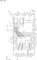
- FIG. 4 is a plan view of a principal portion showing a semiconductor laser device according to a second embodiment of the present disclosure.
- FIG. 6 is a bottom view showing a semiconductor laser device according to a second embodiment of the present disclosure.
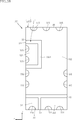
- FIG. 10 is a plan view of a principal portion showing a first modification of the semiconductor laser device according to the second embodiment of the present disclosure.
- FIG. 11 is a bottom view of a main portion showing a first modified example of the semiconductor laser device according to the second embodiment of the present disclosure. It is sectional drawing which follows the XXV-XXV line of FIG.
- FIG. 13 is a plan view of a main portion showing a second modification of the semiconductor laser device according to the second embodiment of the present disclosure.
- FIG. 11 is a bottom view of a main portion showing a second modification of the semiconductor laser device according to the second embodiment of the present disclosure.
- FIG. 11 is a plan view of a principal portion showing a third modification of the semiconductor laser device according to the second embodiment of the present disclosure.
- FIG. 11 is a bottom view of a main portion showing a third modification example of the semiconductor laser device according to the second embodiment of the present disclosure.
- FIG. 9 is a plan view of a principal portion showing a semiconductor laser device according to a third embodiment of the present disclosure.
- FIG. 6 is a bottom view showing a semiconductor laser device according to a third embodiment of the present disclosure.
- FIG. 11 is a plan view of a principal portion showing a first modified example of the semiconductor laser device according to the third embodiment of the present disclosure.
- FIG. 11 is a plan view of a principal portion showing a first modified example of the semiconductor laser device according to the third embodiment of the present disclosure.
- FIG. 11 is a bottom view showing a first modified example of the semiconductor laser device according to the third embodiment of the present disclosure.
- FIG. 9 is a plan view of a principal portion showing a semiconductor laser device according to a fourth embodiment of the present disclosure.
- FIG. 9 is a plan view of a principal portion showing a semiconductor laser device according to a fourth embodiment of the present disclosure.
- FIG. 6 is a bottom view showing a semiconductor laser device according to a fourth embodiment of the present disclosure. It is sectional drawing which follows the XXXVII-XXXVII line of FIG.
- FIG. 13 is a plan view of a principal portion showing a first modified example of the semiconductor laser device according to the fourth embodiment of the present disclosure.
- FIG. 13 is a plan view of a principal portion showing a first modification of the semiconductor laser device according to the fourth embodiment of the present disclosure.
- FIG. 11 is a bottom view showing a first modified example of the semiconductor laser device according to the fourth embodiment of the present disclosure. It is a principal part top view which shows the semiconductor laser device concerning 5th Embodiment of this indication. It is a bottom view showing a semiconductor laser device concerning a 5th embodiment of this indication.
- FIG. 42 is a cross-sectional view taken along line XLIII-XLIII of FIG. 41.
- FIG. 20 is a plan view of a principal portion showing a first modification of the semiconductor laser device according to the fifth embodiment of the present disclosure.
- FIG. 16 is a bottom view showing a first modified example of the semiconductor laser device according to the fifth embodiment of the present disclosure.
- FIG. 20 is a plan view of a principal portion showing a second modification of the semiconductor laser device according to the fifth embodiment of the present disclosure.
- FIG. 16 is a bottom view showing a second modification of the semiconductor laser device according to the fifth embodiment of the present disclosure.
- FIG. 20 is a plan view of a principal portion showing a third modified example of the semiconductor laser device according to the fifth embodiment of the present disclosure.
- FIG. 16 is a bottom view showing a third modified example of the semiconductor laser device according to the fifth embodiment of the present disclosure.
- FIG. 20 is a plan view of a principal portion showing a fourth modified example of the semiconductor laser device according to the fifth embodiment of the present disclosure.
- FIG. 16 is a bottom view showing a fourth modified example of the semiconductor laser device according to the fifth embodiment of the present disclosure.
- FIG. 9 is a plan view of a principal portion showing a semiconductor laser device according to a sixth embodiment of the present disclosure. It is a bottom view showing a semiconductor laser device concerning a 6th embodiment of this indication.
- FIG. 20 is a plan view of a principal portion showing a first modified example of the semiconductor laser device according to the sixth embodiment of the present disclosure.
- FIG. 16 is a bottom view of a main portion showing a first modification of the semiconductor laser device according to the sixth embodiment of the present disclosure. It is a principal part top view which shows the semiconductor laser device concerning 7th Embodiment of this indication.
- FIG. 16 is a main-portion plan view showing a first modified example of the semiconductor laser device according to the seventh embodiment of the present disclosure
- FIG. 16 is a bottom view showing a first modified example of the semiconductor laser device according to the seventh embodiment of the present disclosure.
- the semiconductor laser device A1 of this embodiment includes a support member 1, a semiconductor laser element 4, a switching element 5, a capacitor 6, a first wire 71, a second wire 72, a third wire 73, and a translucent resin 8.
- the semiconductor laser device A1 constitutes, for example, a laser system B1 shown in FIG. 8 and is used as a pulsed laser light source of LiDAR which is an example of two-dimensional distance measurement.
- the application of the semiconductor laser device of the present disclosure is not limited at all.
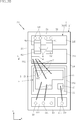
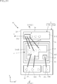
- FIG. 1 is a plan view of an essential part showing the semiconductor laser device A1.
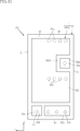
- FIG. 2 is a bottom view showing a semiconductor laser device according to the semiconductor laser device A1.
- FIG. 3 is a sectional view taken along the line III-III in FIG.
- FIG. 4 is a sectional view taken along the line IV-IV in FIG.
- FIG. 5 is a sectional view taken along the line VV of FIG.
- FIG. 6 is a sectional view taken along line VI-VI in FIG.
- FIG. 7 is a sectional view taken along the line VII-VII of FIG.
- FIG. 8 is a circuit diagram showing a laser system B1 including the semiconductor laser device A1.
- the z direction corresponds to the first direction of the present disclosure.
- the transparent resin 8 is omitted for convenience of description.
- the support member 1 forms a conduction path to the semiconductor laser element 4 and the switching element 5 and supports the semiconductor laser element 4 and the switching element 5.
- the specific configuration of the supporting member 1 is not particularly limited, and in the present embodiment, the supporting member 1 has the base material 2 and the conductive portion 3.
- the base material 2 is made of an insulating material.
- the material of the base material 2 is not particularly limited, and examples thereof include epoxy resin and ceramics. In the following description, the case where the base material 2 is made of glass epoxy resin will be described as an example.
- the base material 2 has a main surface 21, a back surface 22, a first surface 23, a second surface 24, a third surface 25 and a fourth surface 26, and has a rectangular shape when viewed in the z direction. Is.
- the main surface 21 is a surface that faces one side in the z direction, and is a flat surface in the illustrated example.
- the back surface 22 is a surface facing the other side in the z direction on the side opposite to the main surface 21, and is a flat surface in the illustrated example.
- the first surface 23 is a surface facing one side in the x direction, and is a flat surface in the illustrated example.
- the second surface 24 is a surface facing the other side in the x direction opposite to the first surface 23, and is a flat surface in the illustrated example.
- the third surface 25 is a surface facing one side in the y direction, and is a flat surface in the illustrated example.
- the fourth surface 26 is a surface facing the other side in the x direction opposite to the third surface 25, and is a flat surface in the illustrated example.
- the conductive portion 3 is a portion that constitutes a conduction path to the semiconductor laser element 4, the switching element 5, and the like.
- the material of the conductive portion 3 is not particularly limited, and examples thereof include metals such as Cu, Ni, Ti, and Au.
- the method for forming the conductive portion 3 is not particularly limited, and in the illustrated example, it is formed by plating, for example.
- the conductive portion 3 of the present embodiment includes a main surface portion 31, a back surface portion 32 and a contact portion 33.
- the main surface portion 31 is arranged on the main surface 21 of the base material 2.
- the principal surface portion 31 includes a principal surface first portion 311, a principal surface second portion 312, a principal surface third portion 313, and a principal surface fourth portion 314.
- the main surface first portion 311 is the second surface 24 side in the x direction of the main surface 21 of the base material 2, and the third surface in the y direction. It is arranged on the 25 side.
- the shape of the main surface first portion 311 is not particularly limited, and in the illustrated example, the main surface first portion 311 is a long rectangular shape having the x direction as the longitudinal direction.
- the main surface first portion 311 is an example of the “first portion” in the present disclosure.
- the main surface first portion 311 of the present embodiment is separated from the second surface 24 and the third surface 25.
- the main surface second portion 312 is arranged closer to the fourth surface 26 in the y direction than the main surface first portion 311.
- the dimension of the main surface second portion 312 in the x direction is larger than the dimension of the main surface first portion 311 in the x direction.
- the main surface second portion 312 overlaps with the main surface first portion 311 when viewed in the y direction.
- the shape of the main surface second portion 312 is not particularly limited, and is rectangular in the illustrated example.
- the area of the main surface second portion 312 is larger than that of the main surface first portion 311, the main surface third portion 313, and the main surface fourth portion 314.
- the main surface second portion 312 of the present embodiment is separated from the first surface 23 and the second surface 24.
- the main surface third portion 313 is arranged closer to the fourth surface 26 in the y direction than the main surface second portion 312.
- the shape of the main surface third portion 313 is not particularly limited, and in the illustrated example, it is a long rectangular shape having the x direction as the longitudinal direction. Further, in the illustrated example, the dimension of the principal surface third portion 313 in the x direction is substantially the same as the dimension of the principal surface second portion 312 in the x direction.
- the principal surface third portion 313 overlaps the principal surface first portion 311 and the principal surface second portion 312 when viewed in the y direction.
- the main surface third portion 313 of the present embodiment is separated from the first surface 23, the second surface 24, and the fourth surface 26.
- the main surface fourth portion 314 is located closer to the first surface 23 in the x direction with respect to the main surface first portion 311, and with respect to the main surface second portion 312. It is located closer to the third surface 25 in the y direction.
- the shape of the main surface fourth portion 314 is not particularly limited, and is rectangular in the illustrated example.
- the y-direction dimension of the principal surface fourth portion 314 is substantially the same as the y-direction dimension of the principal surface first portion 311.
- the dimension of the main surface fourth portion 314 in the x direction is smaller than the dimension of the main surface first portion 311 in the x direction.
- the area of the main surface fourth portion 314 is smaller than the area of the main surface first portion 311.
- the main surface fourth portion 314 overlaps with the main surface first portion 311 when viewed in the x direction. Further, the main surface fourth portion 314 overlaps the main surface second portion 312 and the main surface third portion 313 when viewed in the y direction.
- the main surface fourth portion 314 of the present embodiment is separated from the first surface 23 and the third surface 25.
- the back surface part 32 is arranged on the back surface 22 of the base material 2.
- the back surface portion 32 includes a back surface first portion 321, a back surface second portion 322, a back surface third portion 323, and a back surface fourth portion 324.
- the back surface portion 32 is used as a mounting terminal when mounting the semiconductor laser device A1 on a circuit board (not shown) or the like.
- the back surface first portion 321 is the second surface 24 side in the x direction of the back surface 22 of the base material 2 and the third surface 25 side in the y direction. It is located in.
- the shape of the back surface first portion 321 is not particularly limited, and in the illustrated example, the back surface first portion 321 has a rectangular shape with the longitudinal direction in the x direction.
- the back surface first portion 321 of the present embodiment is separated from the second surface 24 and the third surface 25.
- the back surface second portion 322 is arranged closer to the fourth surface 26 in the y direction than the back surface first portion 321.
- the dimension of the back surface second portion 322 in the x direction is larger than the dimension of the back surface first portion 321 in the x direction.
- the back surface second portion 322 overlaps with the back surface first portion 321 when viewed in the y direction.
- the shape of the second back surface portion 322 is not particularly limited, and is rectangular in the illustrated example.
- the area of the second back surface portion 322 is larger than the area of the first back surface portion 321, the third back surface portion 323, and the fourth back surface portion 324.
- the back surface second portion 322 of the present embodiment is separated from the first surface 23 and the second surface 24.
- the back surface third portion 323 is arranged closer to the fourth surface 26 in the y direction than the back surface second portion 322.
- the shape of the third back surface portion 323 is not particularly limited, and in the illustrated example, the third back surface portion 323 has an oblong shape with the longitudinal direction in the x direction.
- the dimension of the back surface third portion 323 in the x direction is substantially the same as the dimension of the back surface second portion 322 in the x direction.
- the back surface third portion 323 overlaps the back surface first portion 321 and the back surface second portion 322 when viewed in the y direction.
- the back surface third portion 323 of the present embodiment is separated from the first surface 23, the second surface 24, and the fourth surface 26.
- the back surface fourth portion 324 is located closer to the first surface 23 in the x direction than the back surface first portion 321, and is in the y direction with respect to the back surface second portion 322. It is located near the third surface 25.
- the shape of the fourth back surface portion 324 is not particularly limited, and is rectangular in the illustrated example.
- the y-direction dimension of the back surface fourth portion 324 is substantially the same as the y-direction dimension of the back surface first portion 321.
- the dimension of the back surface fourth portion 324 in the x direction is smaller than the dimension of the back surface first portion 321 in the x direction.
- the area of the back surface fourth portion 324 is smaller than the area of the back surface first portion 321.
- the back surface fourth portion 324 overlaps with the back surface first portion 321 when viewed in the x direction.
- the back surface fourth portion 324 overlaps the back surface second portion 322 and the back surface third portion 323 when viewed in the y direction.
- the back surface fourth portion 324 of the present embodiment is separated from the first surface 23 and the third surface 25.
- the contact part 33 makes each part of the main surface part 31 and each part of the back surface part 32 electrically conductive.
- the specific configuration of the communication unit 33 is not particularly limited, and in the illustrated example, as illustrated in FIGS. 1 and 2, a plurality of first communication units 331, a plurality of second communication units 332, and a plurality of third communication units 332.
- the communication unit 333 and the fourth communication unit 334 are included.
- the number of the 1st contact part 331, the 2nd contact part 332, the 3rd contact part 333, and the 4th contact part 334 is not limited at all.
- the specific configurations of the first communication portion 331, the second communication portion 332, the third communication portion 333, and the fourth communication portion 334 are not particularly limited, and in the present embodiment, as shown in FIGS. 1 to 7, z
- An inner region of the base material 2 in a direction view (a region separated from the first surface 23, the second surface 24, the third surface 25, and the fourth surface 26) penetrates the base material 2 in the thickness direction.
- the first communication portion 331, the second communication portion 332, the third communication portion 333, and the fourth communication portion 334 as described above form a plating layer made of metal on the inner surface of the through hole formed in the base material 2. It is provided by the fact that it reaches the main surface 21 and the back surface 22.
- the insides of the first communication portion 331, the second communication portion 332, the third communication portion 333, and the fourth communication portion 334 are filled with resin, but for example, metal is filled. It may be configured.
- the plurality of first connecting portions 331 are connected to the main surface first portion 311 and the back surface first portion 321, and the main surface first portion The part 311 and the first back surface part 321 are connected to each other.
- the plurality of first communication parts 331 are arranged along the x direction.
- the plurality of second connecting portions 332 are connected to the back surface first portion 321 and the back surface second portion 322, and the main surface second portion 312 and the back surface second portion are connected. 322 is connected.
- the plurality of second connecting portions 332 are arranged near the first surface 23 in the x direction.
- the plurality of second connecting portions 332 are arranged in a matrix along the x direction and the y direction.
- the plurality of third connecting portions 333 are connected to the main surface third portion 313 and the back surface third portion 323, and the main surface third portion 313 and The back side third part 323 is connected.
- the plurality of third connecting portions 333 are arranged along the x direction. Further, the plurality of third connecting portions 333 are arranged near the first surface 23 in the x direction.
- the fourth connecting portion 334 is connected to the main surface fourth portion 314 and the back surface fourth portion 324, and the main surface fourth portion 314 and the back surface fourth portion 324. And are connected. Unlike the illustrated example, a configuration having a plurality of fourth connecting portions 334 may be adopted.
- the semiconductor laser element 4 is a light source of the semiconductor laser device A1 and includes an active layer made of a semiconductor layer and the like.
- the semiconductor laser device 4 has a first laser electrode 41 and a second laser electrode 42.
- the first laser electrode 41 is provided on the side facing the main surface 21 in the z direction.
- the second laser electrode 42 is provided on the side facing the back surface 22 in the z direction.
- the first laser electrode 41 is omitted.
- the first laser electrode 41 is an anode electrode and the second laser electrode 42 is a cathode electrode.
- the semiconductor laser device 4 is arranged on the third portion 313 of the main surface. More specifically, the second laser electrode 42 of the semiconductor laser element 4 is conductively bonded to the third main surface portion 313 by the conductive bonding material 49.
- the conductive bonding material 49 is, for example, solder or silver paste.
- the semiconductor laser device 4 is included in the third main surface portion 313 when viewed in the z direction.
- the semiconductor laser element 4 emits the laser light L to the side facing the fourth surface 26 in the y direction. Further, in the illustrated example, the semiconductor laser element 4 overlaps with the one that is located closest to the second surface 24 side in the x direction among the plurality of third connecting portions 333 in the z direction.
- the switching element 5 is an element for turning on/off the current to the semiconductor laser element 4.
- the switching element 5 is a transistor such as an FET made of Si, SiC, GaN, or the like. When the switching element 5 is made of SiC, it is suitable for speeding up switching.
- the switching element 5 of this embodiment has an element body 51, a gate electrode 52, a source electrode 53, and a drain electrode 54, as shown in FIGS. 1, 3, and 6.
- the element body 51 is made of a semiconductor material such as Si or SiC and has an element main surface 511 and an element back surface 512.
- the element main surface 511 is a surface facing the same side as the main surface 21 in the z direction.
- the element back surface 512 is a surface facing the same side as the back surface 22 in the z direction.
- the gate electrode 52 is arranged on the element main surface 511. In the illustrated example, the gate electrode 52 is arranged closer to the first surface 23 in the x direction and closer to the third surface 25 in the y direction.
- the shape of the gate electrode 52 is not particularly limited, and in the illustrated example, it is rectangular when viewed in the z direction.
- the source electrode 53 is arranged on the element main surface 511.
- the source electrode 53 is L-shaped when viewed in the z direction, and is located in the region on the second surface 24 side in the x direction and in the region near the fourth surface 26 in the y direction with respect to the gate electrode 52. It is arranged.
- the drain electrode 54 is arranged on the element back surface 512, and in the illustrated example, covers the substantially entire surface of the element back surface 512.
- the switching element 5 is arranged on the main surface second portion 312 by conductively bonding the drain electrode 54 to the main surface second portion 312 with the conductive bonding material 59.
- the conductive bonding material 59 is, for example, solder or silver paste.
- the switching element 5 is arranged on the second surface 312 of the main surface, closer to the first surface 23 in the x direction. Further, the switching element 5 overlaps with all of the plurality of second connecting portions 332 when viewed in the z direction. The switching element 5 overlaps the semiconductor laser element 4 when viewed in the y direction.
- the capacitor 6 is for temporarily accumulating an electric charge to be a current to be passed through the semiconductor laser element 4.
- the capacitor 6 has an electrode 61 and an electrode 62.
- the electrode 61 is conductively bonded to the third portion 313 of the main surface by the conductive bonding material 69.
- the electrode 62 is conductively bonded to the second main surface portion 312 by the conductive bonding material 69.
- the conductive joining material 69 is, for example, solder. Note that, in FIG. 1, the conductive bonding material 69 is omitted for convenience of description.
- the semiconductor laser device A1 includes two capacitors 6. The two capacitors 6 are connected in parallel with each other. Further, in the present embodiment, the capacitor 6 is arranged closer to the second surface 24 in the x direction than the semiconductor laser element 4 and the switching element 5.
- the plurality of first wires 71 are connected to the source electrode 53 of the switching element 5 and the first laser electrode 41 of the semiconductor laser element 4.
- the first wire 71 is made of a metal such as Au, Cu or Al.
- the number of the plurality of first wires 71 is not particularly limited, and is three in the illustrated example.
- the plurality of first wires 71 are connected to the portion of the source electrode 53 near the fourth surface 26 in the y direction.
- the plurality of first wires 71 are connected to the first laser electrode 41 of the semiconductor laser element 4 so as to be aligned in the y direction.
- the plurality of second wires 72 are connected to the source electrode 53 of the switching element 5 and the main surface first portion 311 of the main surface portion 31 of the conductive portion 3.
- the second wire 72 is made of, for example, a metal such as Au, Cu, Al, or the like, and is made of Au which is the same material as the first wire 71 in the present embodiment.
- the number of the plurality of second wires 72 is not particularly limited, and is two in the illustrated example, which is smaller than the number of the plurality of first wires 71. Therefore, the resistance values of the plurality of first wires 71 are smaller than the resistance values of the plurality of second wires 72.
- the plurality of second wires 72 are connected to the portion of the source electrode 53 near the third surface 25 in the y direction.
- the plurality of second wires 72 are connected to the first main surface portion 311 so as to be aligned in the x direction.
- the third wire 73 is connected to the gate electrode 52 of the switching element 5 and the main surface fourth portion 314 of the main surface portion 31 of the conductive portion 3.
- the third wire 73 is made of, for example, a metal such as Au, Cu or Al, and is made of Au in the present embodiment.
- the number of the third wires 73 is not particularly limited, and is one in the illustrated example.
- the light-transmitting resin 8 is arranged on the main surface 21, and covers the semiconductor laser element 4, the switching element 5, the capacitors 6, the first wires 71, the second wires 72, and the third wires 73. ing.
- the translucent resin 8 is made of a material that transmits the laser light L from the semiconductor laser element 4, and is made of, for example, a transparent epoxy resin or silicone resin.
- the shape of the translucent resin 8 is not particularly limited, and in the present embodiment, as shown in FIGS. 3 to 7, the translucent resin 8 includes the main surface 81, the resin first surface 83, the resin second surface 84, It has a resin third surface 85 and a resin fourth surface 86.
- the main surface 81 is a surface that faces the same side as the main surface 21 in the z direction, and is a flat surface in the illustrated example.
- the resin first surface 83 is a surface facing the same side as the first surface 23 in the x direction. In the illustrated example, the resin first surface 83 is a flat surface and is flush with the first surface 23.
- the resin second surface 84 is a surface facing the same side as the second surface 24 in the x direction. In the illustrated example, the resin second surface 84 is a flat surface and is flush with the second surface 24.
- the resin third surface 85 is a surface facing the same side as the third surface 25 in the y direction. In the illustrated example, the resin third surface 85 is a flat surface and is flush with the third surface 25.
- the resin fourth surface 86 is a surface facing the same side as the fourth surface 26 in the y direction.
- the resin fourth surface 86 is a flat surface and is flush with the resin fourth surface 86.
- the laser light L from the semiconductor laser element 4 is emitted from the resin fourth surface 86 of the translucent resin 8.
- the semiconductor laser device A1 can be used for the laser system B1.
- the laser system B1 includes a semiconductor laser device A1, a gate driver 91, a DC power supply 92, a resistor 93, and a diode 94.
- the gate driver 91 is connected to the gate electrode 52 of the switching element 5 via the back surface fourth portion 324, the fourth connection portion 334, the main surface fourth portion 314, and the third wire 73.
- the gate driver 91 controls the drive voltage applied to the gate electrode 52.
- the DC power source 92 is a power source for causing the semiconductor laser element 4 to emit light.
- the anode electrode of the DC power source 92 is connected to the back surface second portion 322 via the resistor 93.
- the diode 94 is provided between the back surface first portion 321 and the back surface third portion 323, and energizes the current flowing from the back surface third portion 323 to the back surface first portion 321.
- Reference numeral 94 is for preventing excessive reverse voltage application to the semiconductor laser device 4 and for charging the capacitor 6.
- the resistance 93, the back surface second portion 322, the capacitor 6, the back surface third portion 323, the diode 94, and the back surface side are supplied from the DC power supply 92.
- a current IC flows through the path of the first unit 321 and the capacitor 6 is charged.
- the switching element 5 is in the ON state, the electric charge charged in the capacitor 6 flows as a current IL in the path of the switching element 5, the first wire 71, and the semiconductor laser element 4, and the semiconductor laser element 4 is It emits light.
- the current IG flowing when the voltage is applied from the gate driver 91 to the gate electrode 52 of the switching element 5 is mainly from the source electrode 53 to the second electrode. It flows through the wire 72 to the back surface first portion 321.
- the current IL that causes the semiconductor laser element 4 to emit light mainly flows from the source electrode 53 to the semiconductor laser element 4 through the first wire 71. Therefore, the current IL and the current IG mainly flow in different paths. Therefore, for example, the current IL can be suppressed from passing through the current path for applying the gate voltage to the gate electrode 52.
- the source electrode 53 and the semiconductor laser device 4 are directly connected to each other by the first wire 71.
- the inductance component of the path of the current IL can be reduced. Thereby, faster switching is possible and the peak current value of the current IL can be further increased. This is advantageous for emitting the laser light L having a smaller pulse width in a higher output state, and is preferable as a light source device for LiDAR.
- the main surface portion 31 which is a target for mounting the semiconductor laser element 4, the switching element 5, and the capacitor 6 and for connecting the first wire 71, the second wire 72, and the third wire 73, is arranged on the main surface 21, and externally.
- a back surface portion 32 used as a connection terminal for the and are arranged so as to overlap each other when viewed in the z direction. This is suitable for downsizing the semiconductor laser device A1 when viewed in the z direction.
- the main surface portion 31 and the back surface portion 32 are connected by a connecting portion 33.
- the communication part 33 includes a first communication part 331, a second communication part 332, a third communication part 333, and a fourth communication part 334 that penetrate the base material 2.
- Each of the first connecting portion 331, the second connecting portion 332, the third connecting portion 333, and the fourth connecting portion 334 has a shape along the z direction and is not bent. Therefore, it is preferable for reducing the inductance component in the path of the current flowing through the semiconductor laser device A1.
- the switching element 5 and the capacitor 6 are arranged in the x direction.
- the semiconductor laser device 4 is mounted on the third main surface portion 313 located closer to the main surface 21 in the y direction than the switching element 5 and the capacitor 6. Therefore, the path length of the path from the source electrode 53 of the switching element 5 to the main surface second portion 312 via the first wire 71, the semiconductor laser element 4, the main surface third portion 313 and the capacitor 6 is set to be relatively short. Has been done. This is suitable for reducing the inductance component of the path of the current IL in FIG.
- the number of the plurality of first wires 71 is larger than the number of the plurality of second wires 72, and the resistance value of the plurality of first wires 71 is smaller than the resistance value of the plurality of second wires 72.
- a current IL that causes the semiconductor laser element 4 to emit light flows through the plurality of first wires 71.
- the current IL is significantly larger than the current IG. Therefore, the electrical loss can be suppressed by reducing the resistance values of the plurality of first wires 71.
- the number of the plurality of second wires 72 is larger than the number of the third wires 73. As a result, it is possible to suppress electrical loss related to the current IG.
- FIG. 9 shows a first modification of the laser system B1.
- the laser system B11 of this modification includes a resistor 95.
- the resistor 95 is connected in series with the diode 94 between the back surface third portion 323 and the back surface first portion 321. By providing the resistor 95, it is possible to suppress the oscillation of the current value that occurs when the switching element 5 is switched from the ON state to the OFF state.
- FIG. 10 shows a second modification of the laser system B1.
- the laser system B12 of this modification does not include the diode 94 described above.
- a resistor 95 is provided between the back surface first portion 321 and the back surface third portion 323.
- the current can always flow from the back surface first portion 321 to the back surface third portion 323, but the laser system B12 can be operated by adjusting the operating condition.
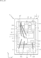
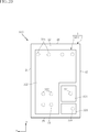
- FIG. 11 is a main part plan view showing a first modification of the semiconductor laser device A1.
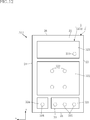
- FIG. 12 is a bottom view showing a first modification of the semiconductor laser device A1.
- the main surface first portion 311 is arranged on the main surface 21 of the base material 2 toward the first surface 23 in the x direction
- the main surface fourth portion 314 is It is arranged near the second surface 24 in the x direction.
- the main surface second portion 312 is arranged closer to the fourth surface 26 in the y direction than the main surface first portion 311 and the main surface fourth portion 314.
- the main surface third portion 313 is arranged closer to the fourth surface 26 in the y direction than the main surface second portion 312.
- the dimensions in the x direction of the main surface second portion 312 and the main surface third portion 313 are substantially the same.
- the back surface first portion 321 is arranged on the back surface 22 of the base material 2 near the first surface 23 in the x direction, and the back surface fourth portion 324 is arranged near the second surface 24 in the x direction.
- the back surface second part 322 is arranged closer to the fourth surface 26 in the y direction than the back surface first part 321 and the back surface fourth part 324.
- the back surface third portion 323 is arranged closer to the fourth surface 26 in the y direction than the back surface second portion 322.
- the back surface second portion 322 and the back surface third portion 323 have substantially the same dimension in the x direction.
- the main surface second portion 312 has a convex portion 3122.
- the convex portion 3122 projects from the portion near the second surface 24 in the x direction toward the fourth surface 26 side in the y direction.
- the main surface third portion 313 has a convex portion 3133.
- the convex portion 3133 projects from the portion near the first surface 23 in the x direction toward the third surface 25 side in the y direction.
- the convex portion 3122 and the convex portion 3133 are lined up in the x direction and overlap each other when viewed in the x direction.
- the switching element 5 is arranged so that the center of the second portion 312 of the main surface in the x direction substantially coincides.
- the gate electrode 52 is arranged closer to the second surface 24 in the x direction, and the source electrode 53 is located closer to the first surface 23 in the x direction and closer to the fourth surface 26 in the y direction than the gate electrode 52. It is located in the area.
- the semiconductor laser element 4 is arranged at a position overlapping the convex portion 3133 when viewed in the y direction.
- the electrode 62 of the capacitor 6 is conductively joined to the convex portion 3122 of the main surface second portion 312.
- the semiconductor laser element 4 and the capacitor 6 are arranged in the x direction and overlap each other when viewed in the x direction. Further, the capacitor 6 overlaps the switching element 5 when viewed in the y direction.
- the inductance component can be reduced. Further, since the switching element 5 and the capacitor 6 overlap each other when viewed in the y direction, the size of the semiconductor laser device A11 in the x direction can be reduced. Further, since the convex portion 3122 and the convex portion 3133 overlap each other when viewed in the x direction, the size of the semiconductor laser device A11 in the y direction can be reduced.
- FIG. 13 is a main part plan view showing a second modification of the semiconductor laser device A1.
- FIG. 14 is a bottom view showing a second modification of the semiconductor laser device A1.
- the semiconductor laser device A12 of the present modification example is different from the above-described semiconductor laser device A11 in that it is provided with two semiconductor laser elements 4.
- the two semiconductor laser elements 4 are arranged side by side in the x direction. Each of the two semiconductor laser elements 4 emits a laser beam L in the y direction.
- Each of the plurality of first wires 71 is connected to the source electrode 53, the first laser electrode 41 of the one semiconductor laser element 4 and the first laser electrode 41 of the other semiconductor laser element 4, and has a bent shape. Is.
- the inductance component can be reduced. Further, by providing the two semiconductor laser elements 4, it is possible to achieve high brightness.
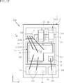
- FIG. 15 is a main part plan view showing a third modification of the semiconductor laser device A1.
- FIG. 16 is a bottom view showing a third modification of the semiconductor laser device A1.
- the semiconductor laser device A13 of the present modification example is different from the semiconductor laser device A12 described above in that the two semiconductor laser elements 4 emit the laser light L in the x direction.
- the two semiconductor laser elements 4 are arranged side by side in the y direction.
- One of the semiconductor laser elements 4 is arranged on the convex portion 3133.
- Each of the two semiconductor laser elements 4 emits a laser beam L in the x direction.
- the inductance component can be reduced. Further, by providing the two semiconductor laser elements 4, it is possible to achieve high brightness. As understood from this modification, the direction in which the laser light L is emitted can be set in various ways.
- FIG. 17 is a main part plan view showing a fourth modification of the semiconductor laser device A1.
- FIG. 18 is a bottom view showing a fourth modification of the semiconductor laser device A1.
- the semiconductor laser device A14 of this modification is different from the above-described semiconductor laser device A13 in the number of semiconductor laser elements 4.
- the number of semiconductor laser elements 4 is one.
- the semiconductor laser device 4 is arranged on the convex portion 3133.
- the inductance component can be reduced.
- the number of semiconductor laser elements 4 can be variously set.
- FIG. 19 is a main part plan view showing a fifth modification of the semiconductor laser device A1.
- FIG. 20 is a bottom view showing a fifth modification of the semiconductor laser device A1.
- the semiconductor laser device A15 of this modification includes a diode 94.
- the diode 94 is provided in series between the principal surface first portion 311 and the principal surface third portion 313, and allows a current flowing from the principal surface third portion 313 to the principal surface first portion 311.
- the diode 94 is mounted on the first main surface portion 311.
- the semiconductor laser element 4 is configured to emit the laser light L in the x direction, but the configuration is not limited to this, and may be configured to emit the laser light L in the y direction, for example.
- the arrangement of the main surface first portion 311, the main surface second portion 312, the main surface third portion 313, the main surface fifth portion 315, the back surface first portion 321, the back surface second portion 322, and the intermediate second portion 342 are There is no limitation as long as it is an arrangement or the like that can configure the circuit configured in the illustrated example.
- the inductance component can be reduced.
- the diode 94 in the semiconductor laser device A15, it is particularly advantageous to reduce the inductance component of the conduction path of the current IC flowing through the diode 94.
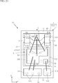
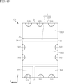
- FIG. 21 is a main-portion plan view showing the semiconductor laser device according to the second embodiment of the present disclosure.
- FIG. 22 is a bottom view showing the semiconductor laser device according to the second embodiment of the present disclosure.
- the main surface second portion 312 has a recess 3121.
- the recessed portion 3121 is a portion in which the portion of the second main surface portion 312 on the fourth surface 26 side in the y direction is recessed toward the third surface 25 side in the y direction.
- the recessed portion 3121 is located at the center of the second portion 312 of the main surface in the x direction.
- the main surface third portion 313 of the present embodiment has a convex portion 3132.
- the convex portion 3132 is a portion of the main surface third portion 313 on the side of the third surface 25 in the y direction that protrudes toward the side of the third surface 25 in the y direction.
- the convex portion 3132 is located at the center of the third surface 313 of the main surface in the x direction. Further, the convex portion 3132 overlaps the concave portion 3121 when viewed in the y direction.
- the semiconductor laser element 4 is arranged at a position overlapping the convex portion 3132 when viewed in the y direction, and overlaps at least a part of the convex portion 3132 when viewed in the z direction.
- the two capacitors 6 are arranged on both sides in the x direction with the semiconductor laser element 4 interposed therebetween. The two capacitors 6 do not overlap the concave portion 3121 and the convex portion 3132 when viewed in the y direction.
- the inductance component can be reduced. Further, since the semiconductor laser element 4 is arranged near the center of the support member 1 in the x direction, it is possible to emit the laser light L from a position closer to the center of the semiconductor laser device A2 in the x direction. ..
- a concave portion 3121 is formed on the main surface second portion 312, and a convex portion 3132 is formed on the main surface third portion 313.
- the concave portion 3121 and the convex portion 3132 overlap each other when viewed in the y direction, and the semiconductor laser element 4 overlaps the concave portion 3121 and the convex portion 3132 when viewed in the y direction. With such a configuration, the size of the semiconductor laser device A2 in the y direction can be reduced.
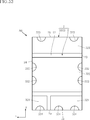
- FIG. 23 is a main part plan view showing a first modification of the semiconductor laser device A2.
- FIG. 24 is a bottom view of essential parts showing a first modification of the semiconductor laser device A2.
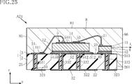
- 25 is a sectional view taken along line XXV-XXV in FIG.
- the base material 2 has a recess 261.
- the recess 261 is a portion that is recessed from the fourth surface 26 toward the third surface 25 side in the y direction.
- the recess 261 is arranged near the center of the base material 2 in the x direction.
- the main surface third portion 313 has a concave portion 3131 and a convex portion 3132.
- the recessed portion 3131 is a portion in which the fourth surface 26 side portion of the main surface third portion 313 in the y direction is recessed toward the third surface 25 side in the y direction.
- the convex portion 3132 is a portion of the main surface third portion 313 on the side of the third surface 25 in the y direction that protrudes toward the side of the third surface 25 in the y direction.
- the concave portion 261, the concave portion 3131, and the convex portion 3132 overlap each other when viewed in the y direction. Further, the recess 261, the recess 3131 and the semiconductor laser element 4 overlap each other.
- the recess 261 is recessed toward the third surface 25 side in the y direction with respect to the resin fourth surface 86 of the translucent resin 8. That is, the recess 261 is separated from the resin fourth surface 86, and the recess 261 is filled with the translucent resin 8.
- the inductance component can be reduced. Further, by having the concave portion 261, the edge of the concave portion 261 and the y-direction edge of the semiconductor laser element 4 (the emission portion of the laser light L) are closer to each other. This makes it possible to prevent the laser light L from interfering with the base material 2. Moreover, since the resin fourth surface 86 is a flat surface, the entire semiconductor laser device A21 has a simple rectangular parallelepiped shape, which is advantageous in that it is easy to carry out work such as transportation and mounting.
- FIG. 26 is a main part plan view showing a second modification of the semiconductor laser device A2.
- FIG. 27 is a bottom view of essential parts showing a second modification of the semiconductor laser device A2.
- the semiconductor laser device A22 of this modified example includes two semiconductor laser elements 4, and other configurations are the same as or similar to those of the semiconductor laser device A2 described above.
- the two semiconductor laser devices 4 are mounted on the third portion 313 of the main surface, and are arranged between the two capacitors 6.
- the two semiconductor laser elements 4 are arranged in the x direction, and each emits the laser light L in the y direction.
- Each of the two semiconductor laser elements 4 and the source electrode 53 of the switching element 5 are connected by a plurality of first wires 71.
- the inductance component can be reduced.
- the provision of the two semiconductor laser elements 4 is advantageous for achieving high brightness.
- the two semiconductor laser elements 4 are collectively arranged near the center of the semiconductor laser device A22 in the x direction, it is preferable for miniaturization of an optical component that refracts or reflects light from the semiconductor laser device A22.
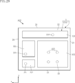
- FIG. 28 is a main-portion plan view showing a third modification of the semiconductor laser device A2.
- FIG. 29 is a bottom view of essential parts showing a third modification of the semiconductor laser device A2.
- the semiconductor laser device A23 of this modification includes a diode 94, and other configurations are the same as or similar to those of the semiconductor laser device A2 described above.
- the main surface first portion 311 is arranged on the second surface 24 side in the x direction with respect to the main surface second portion 312.
- the main surface fourth portion 314 is arranged on the second surface 24 side in the x direction with respect to the main surface second portion 312.
- the principal surface fourth portion 314 is arranged on the third surface 25 side in the y direction with respect to the principal surface first portion 311.
- the diode 94 is provided in series between the principal surface first portion 311 and the principal surface third portion 313, and allows a current flowing from the principal surface third portion 313 to the principal surface first portion 311.
- the diode 94 is mounted on the first main surface portion 311.
- the diode 94 overlaps with the switching element 5 when viewed in the x direction. Further, the diode 94 overlaps the two capacitors 6 when viewed in the x direction.
- the diode 94 does not overlap with the semiconductor laser device 4 when viewed in the x direction.
- the semiconductor laser element 4 is configured to emit the laser light L in the x direction, but the configuration is not limited to this, and may be configured to emit the laser light L in the y direction, for example.
- the arrangement and the like of 342 are not limited as long as the arrangement and the like can configure the circuit configured by the illustrated example.
- the inductance component can be reduced.
- the diode 94 in the semiconductor laser device A15, it is particularly advantageous to reduce the inductance component of the conduction path of the current IC flowing through the diode 94.
- the laser system using the semiconductor laser device A23 can be constructed without using the back surface third part 323. However, by providing the back surface third part 323, the mounting strength and heat dissipation of the semiconductor laser device A23 can be improved. It is possible to improve.
- FIG. 30 is a main-portion plan view showing the semiconductor laser device according to the third embodiment of the present disclosure.
- FIG. 31 is a bottom view showing the semiconductor laser device according to the third embodiment of the present disclosure.
- the configurations of the main surface portion 31, the back surface portion 32, and the connecting portion 33 are different from those of the above-described embodiment.
- the principal surface portion 31 of the present embodiment has a principal surface first portion 311, a principal surface second portion 312, a principal surface third portion 313, a principal surface fourth portion 314, and a principal surface fifth portion 315.
- the arrangement of the first main surface portion 311, the second main surface portion 312, the third main surface portion 313, and the fourth main surface portion 314 is similar to that of the semiconductor laser device A11, for example.
- the main surface second portion 312 does not have the convex portion 3122, and has a rectangular shape when viewed in the z direction.
- the third main surface portion 313 does not have the convex portion 3133, and has a rectangular shape when viewed in the z direction.
- the main surface fifth portion 315 is arranged closer to the fourth surface 26 in the y direction than the main surface third portion 313.
- the shape of the fifth portion 315 of the main surface is not particularly limited, and in the illustrated example, the fifth portion 315 has a rectangular shape whose longitudinal direction is the x direction.
- the second laser electrode 42 is conductively joined to the main surface third portion 313, and is arranged on the main surface third portion 313.
- the electrode 62 of the capacitor 6 is electrically connected to the third portion 313 of the main surface.
- the electrode 61 of the capacitor 6 is conductively joined to the main surface fifth portion 315.
- the back surface first portion 321 is arranged near the third surface 25 in the y direction and near the first surface 23 in the x direction.
- the back surface fourth portion 324 is arranged closer to the second surface 24 in the x direction than the back surface first portion 321.
- the back surface second portion 322 is arranged closer to the fourth surface 26 in the y direction than the back surface first portion 321 and the back surface fourth portion 324.
- the second back surface portion 322 has a recess 3221.
- the recessed portion 3221 is a portion of the back surface second portion 322 on the first surface 23 side in the x direction that is recessed toward the second surface 24 side in the x direction.
- the back surface third portion 323 is arranged so as to overlap the concave portion 3221 in both the x-direction view and the y-direction view.
- the shape of the third back surface part 323 is not particularly limited, and is rectangular in the illustrated example.
- the contact part 33 of the present embodiment includes a first contact part 331, a second contact part 332, a third contact part 333, a fourth contact part 334 and a contact part 335.
- the first connecting portion 331 connects the main surface first portion 311 and the back surface first portion 321.
- the fourth connecting portion 334 connects the main surface fourth portion 314 and the back surface fourth portion 324.
- the third connecting portion 333 connects the main surface third portion 313 and the back surface third portion 323.
- the fourth connecting portion 334 connects the main surface fourth portion 314 and the back surface fourth portion 324.
- the connecting portion 335 connects the main surface fifth portion 315 and the back surface portion 325.
- the plurality of second connecting portions 332 are connected to the portion of the main surface second portion 312 on the fourth surface 26 side in the y direction.
- the inductance component can be reduced.
- the current IL is composed of the first wire 71, the semiconductor laser element 4, the main surface third portion 313, the capacitor 6, the main surface fifth portion 315, the connecting portion 335, and the back surface second portion 322. Flow through the route.
- This path has an annular shape when viewed in the x direction. Therefore, it is possible to further shorten the conduction path as compared with the case where most of the conduction paths for the current IL are formed on the same plane.
- the second connecting portion 332 is arranged closer to the fourth surface 26 in the y direction, the distance between the second connecting portion 332 and the connecting portion 335 in the y direction can be shortened. This is advantageous for shortening the conduction path of the current IL.
- FIG. 32 is a main-portion plan view showing a first modification of the semiconductor laser device A3.
- FIG. 33 is a bottom view showing a first modification of the semiconductor laser device A3.
- the semiconductor laser device A31 of the present modification example is different from the above-described semiconductor laser device A3 in that two semiconductor laser elements 4 are provided.
- the inductance component can be reduced. Further, by providing the two semiconductor laser elements 4, it is possible to achieve high brightness.
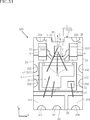
- FIG. 34 is a main-portion plan view showing the semiconductor laser device according to the fourth embodiment of the present disclosure.
- FIG. 35 is a main-portion plan view showing the semiconductor laser device according to the fourth embodiment of the present disclosure.
- FIG. 36 is a bottom view showing the semiconductor laser device according to the fourth embodiment of the present disclosure.
- FIG. 37 is a sectional view taken along line XXXVII-XXXVII in FIG.
- the conductive portion 3 has a main surface portion 31, a back surface portion 32, a connecting portion 33, and an intermediate portion 34. Note that in FIG. 35, the semiconductor laser element 4, the switching element 5, the main surface portion 31, and the first layer 2A described later are omitted.
- the arrangement configuration of the main surface first portion 311, the main surface second portion 312, the main surface third portion 313, and the main surface fourth portion 314 of the main surface portion 31 is the same as that of the semiconductor laser device A3 described above.
- the arrangement configuration of the back surface first portion 321, the back surface second portion 322, the back surface third portion 323, and the back surface fourth portion 324 is similar to that of the semiconductor laser device A2 described above.
- the base material 2 of the present embodiment includes a first layer 2A and a second layer 2B.
- the first layer 2A and the second layer 2B are laminated in the z direction.
- the first layer 2A constitutes the main surface 21.
- the second layer 2B constitutes the back surface 22.
- the intermediate portion 34 is arranged on the main surface 21B of the second layer 2B and is sandwiched between the first layer 2A and the second layer 2B.
- the intermediate section 34 includes an intermediate first section 341, an intermediate second section 342, an intermediate third section 343, and an intermediate fourth section 344.
- the arrangement configuration of the intermediate first portion 341, the intermediate second portion 342, the intermediate third portion 343, and the intermediate fourth portion 344 is as follows: the back surface first portion 321, the back surface second portion 322, the back surface third portion 323, and the back surface fourth portion.
- the arrangement is the same as that of 324.
- the first connecting portion 331 connects the main surface first portion 311, the back surface first portion 321, and the intermediate first portion 341 to each other.
- the second connecting portion 332 connects the main surface second portion 312, the back surface second portion 322, and the intermediate second portion 342 to each other.
- the third connecting portion 333 connects the main surface third portion 313, the back surface third portion 323, and the intermediate third portion 343 to each other.
- the fourth connecting portion 334 connects the main surface fourth portion 314, the back surface fourth portion 324, and the intermediate fourth portion 344 to each other.
- the electrode 61 is conductively joined to the intermediate third portion 343, and the electrode 62 is conductively joined to the intermediate second portion 342.
- a housing portion 25A is formed on the first layer 2A.
- the accommodating portion 25A is a portion capable of accommodating the two capacitors 6.
- a sealing resin 29 is filled between the housing portion 25A and the capacitor 6.
- the inductance component can be reduced. Further, by mounting the capacitor 6 on the intermediate portion 34, for example, the switching element 5 and the capacitor 6 can be overlapped when viewed in the z direction. As a result, the dimensions of the semiconductor laser device A4 in the x direction and the y direction can be reduced.
- the back surface second part 322 and the intermediate second part 342 form a parallel path
- the back surface third part 323 and the intermediate third part 343 form a parallel path. This makes it possible to reduce the resistance and inductance of the path of the current IL.
- FIG. 38 is a main-portion plan view showing a first modification of the semiconductor laser device A4.
- FIG. 39 is a main-portion plan view showing a first modification of the semiconductor laser device A4.
- FIG. 40 is a bottom view showing a first modification of the semiconductor laser device A4.
- the semiconductor laser device A41 of this modification is similar to the above-described semiconductor laser device A3 in the arrangement configuration of the main surface portion 31 and the back surface portion 32.
- the semiconductor laser element 4, the switching element 5, and the capacitor 6 are arranged on the main surface portion 31.
- the intermediate section 34 of the present embodiment has an intermediate first section 341, an intermediate second section 342, an intermediate third section 343, and an intermediate fourth section 344.
- the arrangement configuration of the intermediate first portion 341, the intermediate second portion 342, the intermediate third portion 343, and the intermediate fourth portion 344 is such that the back surface first portion 321, the back surface second portion 322, the back surface third portion 323 of the back surface portion 32 This is the same as the arrangement configuration of the back surface fourth portion 324.
- the second connecting portion 332 is connected to the portion of the main surface second portion 312 on the fourth surface 26 side in the y direction.
- the inductance component can be reduced. Further, by providing the intermediate portion 34 similar to the arrangement configuration of the back surface portion 32, it is possible to reduce the resistance and inductance of the path of the current IL and to reduce the size of the semiconductor laser device A41.
- FIG. 41 is a plan view of relevant parts showing a semiconductor laser device according to the fifth embodiment shown.
- FIG. 42 is a bottom view showing the semiconductor laser device according to the fifth embodiment of the present disclosure.
- 43 is a cross-sectional view taken along the line XLIII-XLIII in FIG. 41.
- the semiconductor laser device A5 of the present embodiment is different from the above-described embodiment mainly in the configuration of the contact portion 33.
- the configuration of the communication section 33 can be appropriately changed to the configuration of the communication section 33 of the present embodiment.
- the arrangement configuration of the main surface portion 31, the back surface portion 32, the semiconductor laser element 4, the switching element 5, the capacitor 6, the first wire 71, the second wire 72, and the third wire 73 of this embodiment is the same as that of the semiconductor laser device A1 described above. Is similar.
- the main surface first portion 311 reaches the second surface 24 and the third surface 25.
- the main surface second portion 312 reaches the first surface 23 and the second surface 24.
- the main surface third portion 313 reaches the first surface 23, the second surface 24, and the fourth surface 26.
- the main surface fourth portion 314 reaches the first surface 23 and the third surface 25.
- the back surface first portion 321 reaches the second surface 24 and the third surface 25.
- the back surface second portion 322 reaches the first surface 23 and the second surface 24.
- the back surface third portion 323 reaches the first surface 23, the second surface 24, and the fourth surface 26.
- the back surface fourth portion 324 reaches the first surface 23 and the third surface 25.
- the connecting portion 33 of the present embodiment has a metal plating layer on the inner surface of the groove provided in the base material 2 along the z direction. It is provided by being formed. Therefore, the connecting portion 33 of the present embodiment is in contact with any of the first surface 23, the second surface 24, the third surface 25, and the fourth surface 26.
- the plurality of first communication parts 331 connect the main surface first part 311 and the back surface first part 321.
- the plurality of first connecting portions 331 are arranged side by side in the x direction along the third surface 25.
- the plurality of second connecting portions 332 connect the main surface second portion 312 and the back surface second portion 322.
- the plurality of second connecting portions 332 are separately arranged on both sides in the x direction. Some of the second connecting portions 332 are arranged side by side in the y direction along the first surface 23. The other part of the second connecting portions 332 are arranged side by side in the y direction along the second surface 24.
- the plurality of third connecting portions 333 connect the main surface third portion 313 and the back surface third portion 323.
- the plurality of third connecting portions 333 are arranged side by side in the x direction along the fourth surface 26.
- the fourth connecting portion 334 connects the main surface fourth portion 314 and the back surface fourth portion 324.
- the fourth connecting portion 334 is in contact with the third surface 25.
- the inductance component can be reduced, and the same effect as that of the semiconductor laser device A1 described above can be obtained.
- FIG. 44 is a main-portion plan view showing a first modification of the semiconductor laser device A5.
- FIG. 45 is a bottom view showing the first modification of the semiconductor laser device A5.
- the arrangement configuration of the main surface portion 31, the back surface portion 32, the semiconductor laser element 4, the switching element 5, the capacitor 6, the first wire 71, the second wire 72, and the third wire 73 of the semiconductor laser device A51 of the present modified example has been described above. It is similar to the semiconductor laser device A11.
- the configurations of the first contact portion 331, the second contact portion 332, the third contact portion 333, and the fourth contact portion 334 of the contact portion 33 are similar to those of the semiconductor laser device A5.
- the inductance component can be reduced, and the same effect as that of the semiconductor laser device A11 described above can be obtained.
- FIG. 46 is a main-portion plan view showing a second modification of the semiconductor laser device A5.
- FIG. 47 is a bottom view showing a second modification of the semiconductor laser device A5.
- the arrangement configuration of the main surface portion 31, the back surface portion 32, the semiconductor laser element 4, the switching element 5, the capacitor 6, the first wire 71, the second wire 72, and the third wire 73 of the semiconductor laser device A52 of this modified example is described above. It is similar to the semiconductor laser device A12.
- the configurations of the first contact portion 331, the second contact portion 332, the third contact portion 333, and the fourth contact portion 334 of the contact portion 33 are similar to those of the semiconductor laser device A5 and the semiconductor laser device A51.
- the plurality of third connecting portions 333 do not overlap the two semiconductor laser elements 4 when viewed in the y direction, and are provided at positions retracted from the two semiconductor laser elements 4.
- the third connecting portion 333 overlaps with the capacitor 6 when viewed in the y direction.
- the inductance component can be reduced, and the same effect as that of the semiconductor laser device A12 described above can be obtained.
- FIG. 48 is a main-portion plan view showing a third modification of the semiconductor laser device according to the fifth embodiment of the present disclosure.
- FIG. 49 is a bottom view showing a third modified example of the semiconductor laser device according to the fifth embodiment of the present disclosure.
- the arrangement configuration of the main surface portion 31, the back surface portion 32, the semiconductor laser element 4, the switching element 5, the capacitor 6, the first wire 71, the second wire 72, and the third wire 73 of the semiconductor laser device A53 of this modified example is described above. It is similar to the semiconductor laser device A14.
- the configurations of the first contact portion 331, the second contact portion 332, the third contact portion 333, and the fourth contact portion 334 of the contact portion 33 are similar to those of the semiconductor laser devices A5, A51, A52.
- one of the plurality of third connecting portions 333 overlaps with the semiconductor laser element 4 when viewed in the y direction.
- the other two third connecting portions 333 overlap the capacitor 6 when viewed in the y direction.
- the inductance component can be reduced, and the same effect as that of the semiconductor laser device A14 described above can be obtained.
- FIG. 50 is a main-portion plan view showing a fourth modification of the semiconductor laser device A5.
- FIG. 51 is a bottom view showing a fourth modification of the semiconductor laser device A5.
- the arrangement configuration of the main surface portion 31, the back surface portion 32, the semiconductor laser element 4, the switching element 5, the capacitor 6, the first wire 71, the second wire 72, and the third wire 73 of the semiconductor laser device A54 of the present modified example has been described above. It is similar to the semiconductor laser device A13.
- the configurations of the first contact portion 331, the second contact portion 332, the third contact portion 333, and the fourth contact portion 334 of the contact portion 33 are similar to those of the semiconductor laser devices A5, A51, A52, A53.
- one of the plurality of third connecting portions 333 overlaps with the two semiconductor laser elements 4 when viewed in the y direction.
- the other two third connecting portions 333 overlap the capacitor 6 when viewed in the y direction.
- the inductance component can be reduced, and the same effect as that of the semiconductor laser device A13 described above can be obtained.
- FIG. 52 is a main-portion plan view showing the semiconductor laser device according to the sixth embodiment of the present disclosure.
- FIG. 53 is a bottom view showing the semiconductor laser device according to the sixth embodiment of the present disclosure.
- the arrangement configuration of the main surface portion 31, the back surface portion 32, the semiconductor laser element 4, the switching element 5, the capacitor 6, the first wire 71, the second wire 72, and the third wire 73 of the semiconductor laser device A6 of the present embodiment has been described above. It is similar to the semiconductor laser device A2.
- the configurations of the first contact portion 331, the second contact portion 332, the third contact portion 333, and the fourth contact portion 334 of the contact portion 33 are similar to those of the semiconductor laser device A5 and the like.
- the two third connecting portions 333 are arranged so as to be separated in the x direction.
- the two third connecting portions 333 overlap the two capacitors 6 when viewed in the y direction, and do not overlap the semiconductor laser element 4.
- the semiconductor laser device 4 is located between the two third connecting portions 333 in the x direction.
- the inductance component can be reduced, and the same effect as that of the semiconductor laser device A2 described above can be obtained.
- FIG. 54 is a main-portion plan view showing a first modification of the semiconductor laser device A6.
- FIG. 55 is a bottom view of essential parts showing a first modification of the semiconductor laser device A6.
- the arrangement configuration of the main surface portion 31, the back surface portion 32, the semiconductor laser element 4, the switching element 5, the capacitor 6, the first wire 71, the second wire 72, and the third wire 73 of the semiconductor laser device A61 of the present modification has been described above. It is similar to the semiconductor laser device A21.
- the configurations of the first contact portion 331, the second contact portion 332, the third contact portion 333, and the fourth contact portion 334 of the contact portion 33 are similar to those of the semiconductor laser device A6.
- the two third connecting portions 333 are arranged so as to be separated in the x direction.
- the two third connecting portions 333 overlap the two capacitors 6 when viewed in the y direction, and do not overlap the semiconductor laser element 4 and the recess 261.
- the semiconductor laser device 4 and the recess 261 are located between the two third connecting portions 333 in the x direction.
- the inductance component can be reduced, and the same effect as that of the semiconductor laser device A21 described above can be obtained.
- FIG. 56 is a main-portion plan view showing the semiconductor laser device according to the seventh embodiment of the present disclosure.
- FIG. 57 is a bottom view showing the semiconductor laser device according to the seventh embodiment of the present disclosure.
- the arrangement configuration of the main surface portion 31, the back surface portion 32, the semiconductor laser element 4, the switching element 5, the capacitor 6, the first wire 71, the second wire 72, and the third wire 73 of the semiconductor laser device A7 of the present embodiment has been described above. It is similar to the semiconductor laser device A3.
- the configurations of the first contact portion 331, the second contact portion 332, the third contact portion 333, and the fourth contact portion 334 of the contact portion 33 are similar to those of the semiconductor laser devices A6, A61 and the like.
- the contact part 33 further includes a contact part 335.
- the connecting portion 335 connects the main surface fifth portion 315 and the back surface second portion 322.
- the two connecting portions 335 overlap the two capacitors 6 when viewed in the y direction.
- the other one connecting portion 335 does not overlap with the capacitor 6 when viewed in the y direction.
- the third connecting portion 333 is provided only on the side opposite to the semiconductor laser element 4 in the x direction.
- the inductance component can be reduced, and the same effect as that of the semiconductor laser device A3 described above can be obtained. Further, since the third connecting portion 333 is provided only on the side opposite to the semiconductor laser element 4 in the x direction, the semiconductor laser element 4 can be brought closer to the first surface 23, and the semiconductor laser element 4 can be moved closer to the first surface 23. It is possible to prevent the laser light L of 1 from interfering with the support member 1.
- FIG. 58 is a main-portion plan view showing a first modification of the semiconductor laser device A7.
- FIG. 59 is a bottom view showing a first modification of the semiconductor laser device A7.
- the arrangement configuration of the main surface portion 31, the back surface portion 32, the semiconductor laser element 4, the switching element 5, the capacitor 6, the first wire 71, the second wire 72, and the third wire 73 of the semiconductor laser device A71 of this modification example is described above. It is similar to the semiconductor laser device A31.
- the configurations of the first contact portion 331, the second contact portion 332, the third contact portion 333, the fourth contact portion 334, and the contact portion 335 of the contact portion 33 are similar to those of the semiconductor laser device A7.
- the two contact portions 335 overlap the two capacitors 6 when viewed in the y direction.
- the other one connecting portion 335 does not overlap with the capacitor 6 when viewed in the y direction.
- the two third connecting portions 333 are provided only on the opposite side of the two semiconductor laser elements 4 in the x direction.
- the two third connecting portions 333 are arranged in the y direction.
- the inductance component can be reduced, and the same effect as that of the semiconductor laser device A31 described above can be obtained. Further, since the third connecting portion 333 is provided only on the side opposite to the semiconductor laser element 4 in the x direction, the semiconductor laser element 4 can be brought closer to the first surface 23, and the semiconductor laser element 4 can be moved closer to the first surface 23. It is possible to prevent the laser light L of 1 from interfering with the support member 1.
- the semiconductor laser device according to the present disclosure is not limited to the above embodiment.
- the specific configuration of each part of the semiconductor laser device according to the present disclosure can be modified in various ways.
- the present disclosure includes configurations related to the following supplementary notes.
- a semiconductor laser device A switching element having a gate electrode, a source electrode and a drain electrode, A support member having a conductive portion that constitutes a conduction path to the switching element and the semiconductor laser element, and supporting the semiconductor laser element and the switching element; Equipped with The conductive portion has a first portion separated from the semiconductor laser device, One or more first wires connected to the source electrode of the switching element and the semiconductor laser element; A semiconductor laser device comprising: one or more second wires connected to the source electrode of the switching element and the first portion of the conductive portion.
- Appendix 2 The semiconductor laser device according to appendix 1, wherein the electrical resistance value of the one or more first wires is smaller than the electrical resistance value of the one or more the second wires.
- the first wire and the second wire are made of the same material, 3.
- the switching element has an element body made of a semiconductor material, The element body has an element main surface and an element back surface that face mutually opposite sides in a first direction that is a thickness direction, The gate electrode and the source electrode are arranged on the element main surface, 4.
- the semiconductor laser device has a first laser electrode arranged on a side facing the device main surface in the first direction, and a second laser electrode arranged on a side facing the device back surface, 5.
- the semiconductor laser device according to appendix 4 wherein the first wire is connected to the first laser electrode.
- the semiconductor laser device according to appendix 6 6.
- the conductive portion has a main surface portion arranged on the main surface and a back surface portion arranged on the back surface.
- the semiconductor laser device according to appendix 7, wherein the conductive portion includes a plurality of connecting portions that electrically connect the main surface portion and the back surface portion.
- Appendix 9 9. The semiconductor laser device according to appendix 8, wherein the main surface portion includes a main surface first portion as the first portion.
- Appendix 10 10. The semiconductor laser device according to appendix 9, wherein the main surface portion includes a main surface second portion to which the drain electrode of the switching element is conductively joined.
- [Appendix 11] 11 11. The semiconductor laser device according to appendix 10, wherein the main surface portion includes a main surface third portion to which the second laser electrode of the semiconductor laser element is conductively joined.
- the main surface portion includes a main surface fourth portion, The semiconductor laser device according to appendix 11, further comprising a third wire connected to the gate electrode and the fourth portion of the main surface.
- the semiconductor laser device according to appendix 12 further comprising a capacitor electrically interposed between the main surface second portion and the main surface third portion.
- the semiconductor laser device according to appendix 13 wherein the capacitor is conductively joined to the main surface second portion and the main surface third portion.
- the back surface portion includes a back surface first portion that is in conduction with the main surface first portion, a back surface second portion that is in conduction with the main surface second portion, a back surface third portion that is in conduction with the main surface third portion, and the main surface. 15.
- the semiconductor laser device according to appendix 14 which includes a back surface fourth portion that is electrically connected to the fourth portion.
- the main surface portion includes a main surface fifth portion, 14.
- the back surface portion includes a back surface first portion that conducts to the principal surface first portion, a back surface second portion that conducts to the principal surface second portion and the principal surface fifth portion, and a back surface that conducts to the principal surface third portion. 17.
- the semiconductor laser device according to appendix 16 comprising a third portion and a back surface fourth portion electrically connected to the main surface fourth portion.
- a diode that is electrically connected in series between the main surface first portion and the main surface third portion and that allows current to flow from the main surface third portion to the main surface first portion is provided.
- [Appendix 19] 19 19. The semiconductor laser device according to appendix 18, wherein the diode is mounted on the first portion of the main surface.
Landscapes
- Physics & Mathematics (AREA)
- Condensed Matter Physics & Semiconductors (AREA)
- General Physics & Mathematics (AREA)
- Electromagnetism (AREA)
- Optics & Photonics (AREA)
- Semiconductor Lasers (AREA)
Abstract
半導体レーザ装置A1は、半導体レーザ素子4と、ゲート電極52、ソース電極53およびドレイン電極54を有するスイッチング素子5と、スイッチング素子5および半導体レーザ素子4への導通経路を構成する導電部3を有し且つ半導体レーザ素子4およびスイッチング素子5を支持する支持部材1と、を備える。導電部3は、半導体レーザ素子4から離間した主面第1部311を有する。半導体レーザ装置A1は、スイッチング素子5のソース電極53と半導体レーザ素子4とに接続された1以上の第1ワイヤ71と、スイッチング素子5のソース電極53と導電部3の主面第1部311とに接続された1以上の第2ワイヤ72と、を備える。このような構成により、半導体レーザ装置A1のインダクタンス成分の低減を図ることができる。
Description
本開示は、半導体レーザ装置に関する。
自動車等に用いられる3次元距離計測に、LiDAR(Light Detection and Ranging、Laser Imaging Detection and Ranging)を用いたシステムが提案されている(たとえば、特許文献1)。LiDARの光源として用いられる半導体レーザ装置は、パルス幅が数十nS以下のパルスレーザ光を出射する。このため、電流の時間変化率が高まり、半導体レーザ装置内のインダクタンス成分に起因する損失が増大する。
本開示は、上記した事情のもとで考え出されたものであって、インダクタンス成分の低減を図ることが可能な半導体レーザ装置を提供することをその課題とする。
本開示によって提供される半導体レーザ装置は、半導体レーザ素子と、ゲート電極、ソース電極およびドレイン電極を有するスイッチング素子と、前記スイッチング素子および前記半導体レーザ素子への導通経路を構成する導電部を有し且つ前記半導体レーザ素子および前記スイッチング素子を支持する支持部材と、を備える半導体レーザ装置であって、前記導電部は、前記半導体レーザ素子から離間した第1部を有し、前記スイッチング素子の前記ソース電極と前記半導体レーザ素子とに接続された1以上の第1ワイヤと、前記スイッチング素子の前記ソース電極と前記導電部の前記第1部とに接続された1以上の第2ワイヤと、を備える。
本開示の半導体レーザ装置によれば、インダクタンス成分の低減を図ることができる。
本開示のその他の特徴および利点は、添付図面を参照して以下に行う詳細な説明によって、より明らかとなろう。
以下、本開示の好ましい実施の形態につき、図面を参照して具体的に説明する。
本開示における「第1」、「第2」、「第3」等の用語は、単にラベルとして用いたものであり、必ずしもそれらの対象物に順列を付することを意図していない。
<第1実施形態>
図1~図8は、本開示の第1実施形態に係る半導体レーザ装置を示している。本実施形態の半導体レーザ装置A1は、支持部材1、半導体レーザ素子4、スイッチング素子5、コンデンサ6、第1ワイヤ71、第2ワイヤ72、第3ワイヤ73および透光樹脂8を備えている。半導体レーザ装置A1は、たとえば図8に示すレーザシステムB1を構成し、2次元距離計測の一例であるLiDARのパルスレーザ光源として用いられる。ただし、本開示の半導体レーザ装置の用途は何ら限定されない。
図1~図8は、本開示の第1実施形態に係る半導体レーザ装置を示している。本実施形態の半導体レーザ装置A1は、支持部材1、半導体レーザ素子4、スイッチング素子5、コンデンサ6、第1ワイヤ71、第2ワイヤ72、第3ワイヤ73および透光樹脂8を備えている。半導体レーザ装置A1は、たとえば図8に示すレーザシステムB1を構成し、2次元距離計測の一例であるLiDARのパルスレーザ光源として用いられる。ただし、本開示の半導体レーザ装置の用途は何ら限定されない。
図1は、半導体レーザ装置A1を示す要部平面図である。図2は、半導体レーザ装置A1に係る半導体レーザ装置を示す底面図である。図3は、図1のIII-III線に沿う断面図である。図4は、図1のIV-IV線に沿う断面図である。図5は、図1のV-V線に沿う断面図である。図6は、図1のVI-VI線に沿う断面図である。図7は、図1のVII-VII線に沿う断面図である。図8は、半導体レーザ装置A1を含むレーザシステムB1を示す回路図である。これらの図において、z方向が本開示の第1方向に相当する。また、図1においては、説明の便宜上、透光樹脂8を省略している。
支持部材1は、半導体レーザ素子4およびスイッチング素子5への導通経路を構成するとともに半導体レーザ素子4およびスイッチング素子5を支持している。支持部材1の具体的構成は特に限定されず、本実施形態においては、支持部材1は、基材2および導電部3を有する。
基材2は、絶縁材料からなる。基材2の材質は特に限定されず、たとえばエポキシ樹脂やセラミックスが挙げられる。以降の説明においては、基材2がガラスエポキシ樹脂からなる場合を例に説明する。本実施形態においては、基材2は、主面21、裏面22、第1面23、第2面24、第3面25および第4面26を有しており、z方向視においてたとえば矩形状である。
主面21は、z方向一方側を向く面であり、図示された例においては、平面である。裏面22は、主面21とは反対側のz方向他方側を向く面であり、図示された例においては、平面である。第1面23は、x方向一方側を向く面であり、図示された例においては、平面である。第2面24は、第1面23とは反対側のx方向他方側を向く面であり、図示された例においては、平面である。第3面25は、y方向一方側を向く面であり、図示された例においては、平面である。第4面26は、第3面25とは反対側のx方向他方側を向く面であり、図示された例においては、平面である。
導電部3は、半導体レーザ素子4およびスイッチング素子5等への導通経路を構成する部位である。導電部3の材質は特に限定されず、Cu,Ni,Ti,Au等の金属が挙げられる。また、導電部3の形成手法は特に限定されず、図示された例においては、たとえばめっきによって形成される。
本実施形態の導電部3は、主面部31、裏面部32および連絡部33を含む。
主面部31は、基材2の主面21上に配置されている。図示された例においては、主面部31は、主面第1部311、主面第2部312、主面第3部313および主面第4部314を含む。
図1、図3、図4および図7に示すように、主面第1部311は、基材2の主面21のx方向における第2面24側であって、y方向における第3面25側に配置されている。主面第1部311の形状は特に限定されず、図示された例においては、x方向を長手方向とする長矩形状である。主面第1部311は、本開示の「第1部」の一例である。本実施形態の主面第1部311は、第2面24および第3面25から離間している。
図1、図3、図4および図6に示すように、主面第2部312は、主面第1部311よりもy方向において第4面26寄りに配置されている。主面第2部312のx方向寸法は、主面第1部311のx方向寸法よりも大きい。主面第2部312は、y方向視において主面第1部311と重なる。主面第2部312の形状は特に限定されず、図示された例においては、矩形状である。主面第2部312の面積は、主面第1部311、主面第3部313および主面第4部314よりも大きい。本実施形態の主面第2部312は、第1面23および第2面24から離間している。
図1、図3、図4および図5に示すように、主面第3部313は、主面第2部312よりもy方向において第4面26寄りに配置されている。主面第3部313の形状は特に限定されず、図示された例においては、x方向を長手方向とする長矩形状である。また、図示された例においては、主面第3部313のx方向寸法は、主面第2部312のx方向寸法と略同じである。主面第3部313は、y方向視において主面第1部311および主面第2部312と重なる。本実施形態の主面第3部313は、第1面23、第2面24および第4面26から離間している。
図1および図7に示すように、主面第4部314は、主面第1部311に対してx方向において第1面23寄りに位置しており、主面第2部312に対してy方向において第3面25寄りに位置している。主面第4部314の形状は特に限定されず、図示された例においては、矩形状である。図示された例においては、主面第4部314のy方向寸法は、主面第1部311のy方向寸法と略同じである。また、主面第4部314のx方向寸法は、主面第1部311のx方向寸法よりも小さい。主面第4部314の面積は、主面第1部311の面積よりも小さい。主面第4部314は、x方向視において主面第1部311と重なる。また、主面第4部314は、y方向視において主面第2部312および主面第3部313と重なる。本実施形態の主面第4部314は、第1面23および第3面25から離間している。
裏面部32は、基材2の裏面22上に配置されている。図示された例においては、裏面部32は、裏面第1部321、裏面第2部322、裏面第3部323および裏面第4部324を含む。本実施形態においては、裏面部32は、半導体レーザ装置A1を回路基板(図示略)等に実装する際の実装端子として用いられる。
図1、図3、図4および図7に示すように、裏面第1部321は、基材2の裏面22のx方向における第2面24側であって、y方向における第3面25側に配置されている。裏面第1部321の形状は特に限定されず、図示された例においては、x方向を長手方向とする長矩形状である。本実施形態の裏面第1部321は、第2面24および第3面25から離間している。
図2、図3、図4および図6に示すように、裏面第2部322は、裏面第1部321よりもy方向において第4面26寄りに配置されている。裏面第2部322のx方向寸法は、裏面第1部321のx方向寸法よりも大きい。裏面第2部322は、y方向視において裏面第1部321と重なる。裏面第2部322の形状は特に限定されず、図示された例においては、矩形状である。裏面第2部322の面積は、裏面第1部321、裏面第3部323および裏面第4部324よりも大きい。本実施形態の裏面第2部322は、第1面23および第2面24から離間している。
図2、図3、図4および図5に示すように、裏面第3部323は、裏面第2部322よりもy方向において第4面26寄りに配置されている。裏面第3部323の形状は特に限定されず、図示された例においては、x方向を長手方向とする長矩形状である。また、図示された例においては、裏面第3部323のx方向寸法は、裏面第2部322のx方向寸法と略同じである。裏面第3部323は、y方向視において裏面第1部321および裏面第2部322と重なる。本実施形態の裏面第3部323は、第1面23、第2面24および第4面26から離間している。
図2および図7に示すように、裏面第4部324は、裏面第1部321に対してx方向において第1面23寄りに位置しており、裏面第2部322に対してy方向において第3面25寄りに位置している。裏面第4部324の形状は特に限定されず、図示された例においては、矩形状である。図示された例においては、裏面第4部324のy方向寸法は、裏面第1部321のy方向寸法と略同じである。また、裏面第4部324のx方向寸法は、裏面第1部321のx方向寸法よりも小さい。裏面第4部324の面積は、裏面第1部321の面積よりも小さい。裏面第4部324は、x方向視において裏面第1部321と重なる。また、裏面第4部324は、y方向視において裏面第2部322および裏面第3部323と重なる。本実施形態の裏面第4部324は、第1面23および第3面25から離間している。
連絡部33は、主面部31の各部と裏面部32の各部とを導通させる。連絡部33の具体的構成は特に限定されず、図示された例においては、図1および図2に示すように、複数の第1連絡部331、複数の第2連絡部332、複数の第3連絡部333および第4連絡部334を含む。なお、第1連絡部331、第2連絡部332、第3連絡部333および第4連絡部334の個数は、何ら限定されない。
第1連絡部331、第2連絡部332、第3連絡部333および第4連絡部334の具体的構成は特に限定されず、本実施形態においては、図1~図7に示すように、z方向視における基材2の内方領域(第1面23、第2面24、第3面25および第4面26から離間した領域)において、基材2を厚さ方向に貫通している。このような、第1連絡部331、第2連絡部332、第3連絡部333および第4連絡部334は、基材2に形成された貫通孔の内面に、金属からなるめっき層を形成することによって設けられており、主面21および裏面22に到達している。なお、図示された例においては、第1連絡部331、第2連絡部332、第3連絡部333および第4連絡部334の内部は、樹脂が充填された構成であるが、たとえば金属が充填された構成であってもよい。
図1、図2、図3、図4および図7に示すように、複数の第1連絡部331は、主面第1部311と裏面第1部321とに繋がっており、主面第1部311と裏面第1部321とを連結している。本実施形態においては、複数の第1連絡部331は、x方向に沿って配列されている。
図1、図2および図6に示すように、複数の第2連絡部332は、裏面第1部321と裏面第2部322とに繋がっており、主面第2部312と裏面第2部322とを連結している。本実施形態においては、複数の第2連絡部332は、x方向において第1面23寄りに配置されている。図示された例においては、複数の第2連絡部332は、x方向およびy方向に沿ったマトリクス状に配置されている。
図1、図2、図3および図5に示すように、複数の第3連絡部333は、主面第3部313と裏面第3部323とに繋がっており、主面第3部313と裏面第3部323とを連結している。本実施形態においては、複数の第3連絡部333は、x方向に沿って配列されている。また、複数の第3連絡部333は、x方向において第1面23寄りに配置されている。
図1、図2および図7に示すように、第4連絡部334は、主面第4部314と裏面第4部324とに繋がっており、主面第4部314と裏面第4部324とを連結している。図示された例とは異なり、複数の第4連絡部334を有する構成であってもよい。
半導体レーザ素子4は、半導体レーザ装置A1の光源であり、半導体層からなる活性層等を含む。本実施形態においては、図3に示すように、半導体レーザ素子4は、第1レーザ電極41および第2レーザ電極42を有する。第1レーザ電極41は、z方向において主面21が向く側に設けられている。第2レーザ電極42は、z方向において裏面22が向く側に設けられている。図1においては、第1レーザ電極41を省略している。本実施形態においては、第1レーザ電極41がアノード電極であり、第2レーザ電極42がカソード電極である。
図1および図3に示すように、本実施形態においては、半導体レーザ素子4は、主面第3部313上に配置されている。より具体的には、半導体レーザ素子4の第2レーザ電極42が導電性接合材49によって主面第3部313に導通接合されている。導電性接合材49は、たとえばはんだや銀ペーストである。図示された例においては、半導体レーザ素子4は、z方向視において主面第3部313に内包されている。半導体レーザ素子4は、y方向において第4面26が向く側にレーザ光Lを出射する。また、図示された例においては、半導体レーザ素子4は、複数の第3連絡部333のうちx方向において最も第2面24側に位置するものとz方向視において重なっている。
スイッチング素子5は、半導体レーザ素子4への電流をON/OFFするための素子である。スイッチング素子5は、たとえばSiやSiC、あるいはGaN等からなるFET等のトランジスタである。スイッチング素子5がSiCからなる場合、スイッチングの高速化を図るのに適している。本実施形態のスイッチング素子5は、図1、図3および図6に示すように、素子本体51、ゲート電極52、ソース電極53およびドレイン電極54を有する。素子本体51は、SiやSiC等の半導体材料からなり、素子主面511および素子裏面512を有する。素子主面511は、z方向において主面21と同じ側を向く面である。素子裏面512は、z方向において裏面22と同じ側を向く面である。
ゲート電極52は、素子主面511上に配置されている。図示された例においては、ゲート電極52は、x方向において第1面23寄りに配置されており、y方向において第3面25寄りに配置されている。ゲート電極52の形状は特に限定されず、図示された例においては、z方向視において矩形状である。
ソース電極53は、素子主面511上に配置されている。図示された例においては、ソース電極53は、z方向視においてL字状であり、ゲート電極52に対してx方向における第2面24側の領域およびy方向における第4面26寄りの領域に配置されている。
ドレイン電極54は、素子裏面512上に配置されており、図示された例においては、素子裏面512の略全面を覆っている。
スイッチング素子5は、ドレイン電極54が導電性接合材59によって主面第2部312に導通接合されることにより、主面第2部312上に配置されている。導電性接合材59は、たとえばはんだや銀ペーストである。本実施形態においては、スイッチング素子5は、主面第2部312上において、x方向における第1面23寄りに配置されている。また、スイッチング素子5は、z方向視において複数の第2連絡部332のすべてと重なっている。スイッチング素子5は、y方向視において半導体レーザ素子4と重なる。
コンデンサ6は、半導体レーザ素子4に通電する電流となるべき電荷を一時的に蓄積するためのものである。図1および図4に示すように、図示された例においては、コンデンサ6は、電極61および電極62を有する。電極61は、導電性接合材69によって主面第3部313に導通接合されている。電極62は、導電性接合材69によって主面第2部312に導通接合されている。導電性接合材69は、たとえばはんだである。なお、図1においては、説明の便宜上、導電性接合材69を省略している。また、本実施形態においては、半導体レーザ装置A1は、2つのコンデンサ6を備える。2つのコンデンサ6は、互いに並列に接続されている。また、本実施形態においては、コンデンサ6は、半導体レーザ素子4およびスイッチング素子5に対して、x方向において第2面24寄りに配置されている。
複数の第1ワイヤ71は、図1および図3に示すように、スイッチング素子5のソース電極53と半導体レーザ素子4の第1レーザ電極41とに接続されている。第1ワイヤ71は、たとえば、Au、Cu、Al等の金属からなる。複数の第1ワイヤ71の本数は特に限定されず、図示された例においては、3本である。複数の第1ワイヤ71は、ソース電極53のy方向における第4面26寄りの部分に接続されている。複数の第1ワイヤ71は、半導体レーザ素子4の第1レーザ電極41に、y方向に並ぶように接続されている。
複数の第2ワイヤ72は、図1および図3に示すように、スイッチング素子5のソース電極53と導電部3の主面部31の主面第1部311とに接続されている。第2ワイヤ72は、たとえば、Au、Cu、Al等の金属からなり、本実施形態においては、第1ワイヤ71と同じ材質であるAuからなる。複数の第2ワイヤ72の本数は特に限定されず、図示された例においては、2本であり、複数の第1ワイヤ71の本数よりも少ない。このため、複数の第1ワイヤ71の抵抗値は、複数の第2ワイヤ72の抵抗値よりも小さい。複数の第2ワイヤ72は、ソース電極53のy方向における第3面25寄りの部分に接続されている。複数の第2ワイヤ72は、主面第1部311に、x方向に並ぶように接続されている。
第3ワイヤ73は、図1に示すように、スイッチング素子5のゲート電極52と導電部3の主面部31の主面第4部314とに接続されている。第3ワイヤ73は、たとえば、Au、Cu、Al等の金属からなり、本実施形態においては、Auからなる。第3ワイヤ73の本数は特に限定されず、図示された例においては、1本である。
透光樹脂8は、主面21上に配置されており、半導体レーザ素子4、スイッチング素子5、複数のコンデンサ6、複数の第1ワイヤ71、複数の第2ワイヤ72および第3ワイヤ73を覆っている。透光樹脂8は、半導体レーザ素子4からのレーザ光Lを透過させる材質からなり、たとえば透明なエポキシ樹脂やシリコーン樹脂からなる。
透光樹脂8の形状は特に限定されず、本実施形態においては、図3~図7に示すように、透光樹脂8は、主面81、樹脂第1面83、樹脂第2面84、樹脂第3面85および樹脂第4面86を有する。
主面81は、z方向において主面21と同じ側を向く面であり、図示された例においては、平面である。樹脂第1面83は、x方向において第1面23と同じ側を向く面である。図示された例においては、樹脂第1面83は、平面であり、第1面23と面一である。樹脂第2面84は、x方向において第2面24と同じ側を向く面である。図示された例においては、樹脂第2面84は、平面であり、第2面24と面一である。樹脂第3面85は、y方向において第3面25と同じ側を向く面である。図示された例においては、樹脂第3面85は、平面であり、第3面25と面一である。樹脂第4面86は、y方向において第4面26と同じ側を向く面である。図示された例においては、樹脂第4面86は、平面であり、樹脂第4面86と面一である。本実施形態においては、半導体レーザ素子4からのレーザ光Lは、透光樹脂8の樹脂第4面86から出射される。なお、樹脂第4面86を平坦かつ平滑な面とすることにより、レーザ光Lの散乱を抑制し、出射効率を高めることができる。
図8に示すように、半導体レーザ装置A1は、レーザシステムB1に用いることができる。レーザシステムB1は、半導体レーザ装置A1とゲートドライバ91、直流電源92、抵抗93およびダイオード94を備える。
ゲートドライバ91は、裏面第4部324、第4連絡部334、主面第4部314および第3ワイヤ73を介してスイッチング素子5のゲート電極52に接続されている。ゲートドライバ91は、ゲート電極52に印加する駆動電圧を制御する。
直流電源92は、半導体レーザ素子4を発光させるための電源である。直流電源92のアノード電極は、抵抗93を介して裏面第2部322に接続されている。
ダイオード94は、裏面第1部321と裏面第3部323との間に設けられており、裏面第3部323から裏面第1部321に向かう電流を通電させる。94は、半導体レーザ素子4への過大な逆電圧印加を防止するとともに、コンデンサ6への充電を実現するためのものである。
このような構成のレーザシステムB1においては、スイッチング素子5がOFFの状態の場合に、直流電源92から、抵抗93、裏面第2部322、コンデンサ6、裏面第3部323、ダイオード94、裏面第1部321の経路に電流ICが流れ、コンデンサ6に充電される。そして、スイッチング素子5がONの状態の場合に、コンデンサ6に充電された電荷が、スイッチング素子5、第1ワイヤ71、半導体レーザ素子4の経路に電流ILとなって流れ、半導体レーザ素子4が発光する。
次に、半導体レーザ装置A1の作用について説明する。
本実施形態によれば、図1および図8に示すように、ゲートドライバ91からスイッチング素子5のゲート電極52に電圧が印加されることにより流れる電流IGは、主に、ソース電極53から第2ワイヤ72を通じて裏面第1部321へと流れる。一方、半導体レーザ素子4を発光させる電流ILは、主に、ソース電極53から第1ワイヤ71を通じて半導体レーザ素子4へと流れる。このため、電流ILと電流IGとは、主に、互いに異なる経路を流れる。このため、たとえば電流ILがゲート電極52にゲート電圧を印加するための電流経路を通ることを抑制可能である。また、ソース電極53と半導体レーザ素子4とは、第1ワイヤ71によって互いに直接接続されている。したがって、電流ILの経路のインダクタンス成分を低減可能である。これにより、より高速なスイッチングが可能であるとともに、電流ILのピーク電流値をさらに高めることができる。これは、よりパルス幅が小さいレーザ光Lを、より高出力な状態で出射するのに有利であり、LiDARの光源デバイスとして好ましい。
半導体レーザ素子4、スイッチング素子5およびコンデンサ6の実装や第1ワイヤ71、第2ワイヤ72および第3ワイヤ73の接続の対象である主面部31が、主面21上に配置されており、外部との接続端子として用いられる裏面部32とが、z方向視において互いに重なるように配置されている。これは、半導体レーザ装置A1のz方向視における小型化に適している。また、主面部31と裏面部32とは連絡部33によって連結されている。連絡部33は、基材2を貫通する第1連絡部331、第2連絡部332、第3連絡部333および第4連絡部334を含む。第1連絡部331、第2連絡部332、第3連絡部333および第4連絡部334は、いずれもz方向に沿った形状であり、屈曲していない。このため、半導体レーザ装置A1を流れる電流の経路におけるインダクタンス成分の低減に好ましい。
図1に示すように、スイッチング素子5とコンデンサ6とは、x方向において並べられている。半導体レーザ素子4は、スイッチング素子5およびコンデンサ6に対してy方向において主面21寄りに位置する主面第3部313に搭載されている。このため、スイッチング素子5のソース電極53から第1ワイヤ71、半導体レーザ素子4、主面第3部313およびコンデンサ6を介して主面第2部312に至る経路の経路長が比較的短く設定されている。これは、図8における電流ILの経路のインダクタンス成分を低減するのに適している。
複数の第1ワイヤ71の本数は、複数の第2ワイヤ72の本数よりも多く、複数の第1ワイヤ71の抵抗値は、複数の第2ワイヤ72の抵抗値よりも小さい。複数の第1ワイヤ71には、半導体レーザ素子4を発光させる電流ILが流れる。電流ILは、電流IGよりも顕著に大きい。したがって、複数の第1ワイヤ71の抵抗値を低減させることにより、電気的損失を抑制することができる。
複数の第2ワイヤ72の本数は、第3ワイヤ73の本数よりも多い。これにより、電流IGに関する電気的損失を抑制することができる。
図9~図59は、本開示の変形例および他の実施形態を示している。なお、これらの図において、上記実施形態と同一または類似の要素には、上記実施形態と同一の符号を付している。
<レーザシステムB1 第1変形例>
図9は、レーザシステムB1の第1変形例を示している。本変形例のレーザシステムB11は、抵抗95を備える。抵抗95は、裏面第3部323と裏面第1部321との間において、ダイオード94と直列に接続されている。抵抗95を備えることにより、スイッチング素子5が、ON状態からOFF状態に切り替えられた際に生じる電流値の振動を抑制することができる。
図9は、レーザシステムB1の第1変形例を示している。本変形例のレーザシステムB11は、抵抗95を備える。抵抗95は、裏面第3部323と裏面第1部321との間において、ダイオード94と直列に接続されている。抵抗95を備えることにより、スイッチング素子5が、ON状態からOFF状態に切り替えられた際に生じる電流値の振動を抑制することができる。
<レーザシステムB1 第2変形例>
図10は、レーザシステムB1の第2変形例を示している。本変形例のレーザシステムB12は、上述のダイオード94を備えていない。裏面第1部321と裏面第3部323との間には、抵抗95が設けられている。本変形例においては、裏面第1部321から裏面第3部323へと常に電流が流れうる状態ではあるが、動作条件を調整することにより、レーザシステムB12を動作させることができる。
図10は、レーザシステムB1の第2変形例を示している。本変形例のレーザシステムB12は、上述のダイオード94を備えていない。裏面第1部321と裏面第3部323との間には、抵抗95が設けられている。本変形例においては、裏面第1部321から裏面第3部323へと常に電流が流れうる状態ではあるが、動作条件を調整することにより、レーザシステムB12を動作させることができる。
<第1実施形態 第1変形例>
図11は、半導体レーザ装置A1の第1変形例を示す要部平面図である。図12は、半導体レーザ装置A1の第1変形例を示す底面図である。本変形例の半導体レーザ装置A11においては、主面第1部311は、基材2の主面21上においてx方向における第1面23寄りに配置されており、主面第4部314は、x方向における第2面24寄りに配置されている。主面第2部312は、主面第1部311および主面第4部314に対してy方向における第4面26寄りに配置されている。主面第3部313は、主面第2部312に対してy方向における第4面26寄りに配置されている。主面第2部312と主面第3部313とのx方向寸法は、略同じである。
図11は、半導体レーザ装置A1の第1変形例を示す要部平面図である。図12は、半導体レーザ装置A1の第1変形例を示す底面図である。本変形例の半導体レーザ装置A11においては、主面第1部311は、基材2の主面21上においてx方向における第1面23寄りに配置されており、主面第4部314は、x方向における第2面24寄りに配置されている。主面第2部312は、主面第1部311および主面第4部314に対してy方向における第4面26寄りに配置されている。主面第3部313は、主面第2部312に対してy方向における第4面26寄りに配置されている。主面第2部312と主面第3部313とのx方向寸法は、略同じである。
裏面第1部321は、基材2の裏面22上においてx方向における第1面23寄りに配置されており、裏面第4部324は、x方向における第2面24寄りに配置されている。裏面第2部322は、裏面第1部321および裏面第4部324に対してy方向における第4面26寄りに配置されている。裏面第3部323は、裏面第2部322に対してy方向における第4面26寄りに配置されている。裏面第2部322と裏面第3部323とのx方向寸法は、略同じである。
本例においては、主面第2部312は、凸部3122を有する。凸部3122は、x方向における第2面24寄りの部分からy方向における第4面26側に突出している。主面第3部313は、凸部3133を有する。凸部3133は、x方向における第1面23寄りの部分からy方向における第3面25側に突出している。凸部3122と凸部3133とは、x方向に並んでおり、x方向視において重なる。
スイッチング素子5は、主面第2部312とx方向中央が略一致するように配置されている。ゲート電極52は、x方向において第2面24寄りに配置されており、ソース電極53は、ゲート電極52に対してx方向における第1面23寄りの領域およびy方向における第4面26寄りの領域に配置されている。
半導体レーザ素子4は、y方向視において凸部3133と重なる位置に配置されている。コンデンサ6の電極62は、主面第2部312の凸部3122に導通接合されている。半導体レーザ素子4とコンデンサ6とは、x方向に並んでおり、x方向視において互いに重なる。また、コンデンサ6は、y方向視においてスイッチング素子5と重なる。
本変形例によっても、インダクタンス成分を低減可能である。また、スイッチング素子5とコンデンサ6とがy方向視において重なる構成であることにより、半導体レーザ装置A11のx方向寸法を縮小することができる。また、凸部3122と凸部3133とがx方向視において重なる構成であることにより、半導体レーザ装置A11のy方向寸法を縮小することができる。
<第1実施形態 第2変形例>
図13は、半導体レーザ装置A1の第2変形例を示す要部平面図である。図14は、半導体レーザ装置A1の第2変形例を示す底面図である。本変形例の半導体レーザ装置A12は、2つの半導体レーザ素子4を備えている点が、上述した半導体レーザ装置A11と異なっている。
図13は、半導体レーザ装置A1の第2変形例を示す要部平面図である。図14は、半導体レーザ装置A1の第2変形例を示す底面図である。本変形例の半導体レーザ装置A12は、2つの半導体レーザ素子4を備えている点が、上述した半導体レーザ装置A11と異なっている。
2つの半導体レーザ素子4は、x方向に並んで配置されている。2つの半導体レーザ素子4は、それぞれがy方向にレーザ光Lを出射する。
複数の第1ワイヤ71は、各々が、ソース電極53と一方の半導体レーザ素子4の第1レーザ電極41と他方の半導体レーザ素子4の第1レーザ電極41とに接続されており、屈曲した形状である。
本変形例によっても、インダクタンス成分を低減可能である。また、2つの半導体レーザ素子4を備えることにより、高輝度化を図ることができる。
<第1実施形態 第3変形例>
図15は、半導体レーザ装置A1の第3変形例を示す要部平面図である。図16は、半導体レーザ装置A1の第3変形例を示す底面図である。本変形例の半導体レーザ装置A13は、2つの半導体レーザ素子4が、x方向にレーザ光Lを出射する点が、上述した半導体レーザ装置A12と異なっている。
図15は、半導体レーザ装置A1の第3変形例を示す要部平面図である。図16は、半導体レーザ装置A1の第3変形例を示す底面図である。本変形例の半導体レーザ装置A13は、2つの半導体レーザ素子4が、x方向にレーザ光Lを出射する点が、上述した半導体レーザ装置A12と異なっている。
2つの半導体レーザ素子4は、y方向に並んで配置されている。一方の半導体レーザ素子4は、凸部3133に配置されている。2つの半導体レーザ素子4は、それぞれがx方向にレーザ光Lを出射する。
本変形例によっても、インダクタンス成分を低減可能である。また、2つの半導体レーザ素子4を備えることにより、高輝度化を図ることができる。本変形例から理解されるように、レーザ光Lが出射される方向は、種々に設定可能である。
<第1実施形態 第4変形例>
図17は、半導体レーザ装置A1の第4変形例を示す要部平面図である。図18は、半導体レーザ装置A1の第4変形例を示す底面図である。本変形例の半導体レーザ装置A14は、半導体レーザ素子4の個数が上述した半導体レーザ装置A13と異なる。
図17は、半導体レーザ装置A1の第4変形例を示す要部平面図である。図18は、半導体レーザ装置A1の第4変形例を示す底面図である。本変形例の半導体レーザ装置A14は、半導体レーザ素子4の個数が上述した半導体レーザ装置A13と異なる。
本変形例においては、半導体レーザ素子4の個数は、1つである。半導体レーザ素子4は、凸部3133上に配置されている。
本変形例によっても、インダクタンス成分を低減可能である。半導体レーザ装置A13および本変形例から理解されるように、半導体レーザ素子4の個数は、種々に設定可能である。
<第1実施形態 第5変形例>
図19は、半導体レーザ装置A1の第5変形例を示す要部平面図である。図20は、半導体レーザ装置A1の第5変形例を示す底面図である。本変形例の半導体レーザ装置A15は、ダイオード94を備える。
図19は、半導体レーザ装置A1の第5変形例を示す要部平面図である。図20は、半導体レーザ装置A1の第5変形例を示す底面図である。本変形例の半導体レーザ装置A15は、ダイオード94を備える。
ダイオード94は、主面第1部311と主面第3部313との間に直列に設けられており、主面第3部313から主面第1部311に向かう電流を許容する。図示された例においては、ダイオード94は、主面第1部311に搭載されている。
図示された例においては、半導体レーザ素子4は、x方向にレーザ光Lを出射する構成であるが、これに限定されず、たとえばy方向にレーザ光Lを出射する構成であってもよい。主面第1部311、主面第2部312、主面第3部313、主面第5部315、裏面第1部321、裏面第2部322および中間第2部342の配置等は、図示された例が構成する回路を構成しうる配置等であれば、何ら限定されない。
本変形例によっても、インダクタンス成分を低減可能である。ダイオード94を半導体レーザ装置A15内に内蔵していることにより、特に、ダイオード94を流れる上述の電流ICの導通経路のインダクタンス成分を低減するのに有利である。
<第2実施形態>
図21は、本開示の第2実施形態に係る半導体レーザ装置を示す要部平面図である。図22は、本開示の第2実施形態に係る半導体レーザ装置を示す底面図である。
図21は、本開示の第2実施形態に係る半導体レーザ装置を示す要部平面図である。図22は、本開示の第2実施形態に係る半導体レーザ装置を示す底面図である。
本実施形態の半導体レーザ装置A2においては、主面第2部312が、凹部3121を有する。凹部3121は、主面第2部312のy方向における第4面26側の部分が、y方向において第3面25側に凹んだ部位である。凹部3121は、主面第2部312のx方向中央に位置する。
本実施形態の主面第3部313は、凸部3132を有する。凸部3132は、主面第3部313のy方向における第3面25側の部分が、y方向において第3面25側に突出した部分である。凸部3132は、主面第3部313のx方向中央に位置する。また、凸部3132は、y方向視において凹部3121と重なる。
半導体レーザ素子4は、y方向視において凸部3132と重なる位置に配置されており、z方向視において凸部3132の少なくとも一部と重なっている。2つのコンデンサ6は、半導体レーザ素子4を挟んでx方向両側に配置されている。2つのコンデンサ6は、y方向視において凹部3121および凸部3132と重なっていない。
本実施形態によっても、インダクタンス成分を低減可能である。また、半導体レーザ素子4が、支持部材1のx方向中央寄りに配置されていることにより、半導体レーザ装置A2のx方向中心に対してより近い位置からレーザ光Lを出射することが可能である。
主面第2部312に凹部3121が形成され、主面第3部313に凸部3132が形成されている。凹部3121と凸部3132とがy方向視において重なり、半導体レーザ素子4がy方向視において凹部3121および凸部3132と重なる。このような構成により、半導体レーザ装置A2のy方向寸法を縮小することができる。
<第2実施形態 第1変形例>
図23は、半導体レーザ装置A2の第1変形例を示す要部平面図である。図24は、半導体レーザ装置A2の第1変形例を示す要部底面図である。図25は、図23のXXV-XXV線に沿う断面図である。
図23は、半導体レーザ装置A2の第1変形例を示す要部平面図である。図24は、半導体レーザ装置A2の第1変形例を示す要部底面図である。図25は、図23のXXV-XXV線に沿う断面図である。
本変形例の半導体レーザ装置A21においては、基材2が、凹部261を有する。凹部261は、第4面26からy方向における第3面25側に凹んだ部位である。凹部261は、基材2のx方向中央寄りに配置されている。主面第3部313は、凹部3131および凸部3132を有する。凹部3131は、主面第3部313のy方向における第4面26側部分がy方向において第3面25側に凹んだ部位である。凸部3132は、主面第3部313のy方向における第3面25側の部分が、y方向において第3面25側に突出した部分である。凹部261、凹部3131および凸部3132は、y方向視において互いに重なる。また、凹部261および凹部3131と半導体レーザ素子4とは、互いに重なる。
図25に示すように、凹部261は、透光樹脂8の樹脂第4面86に対してy方向における第3面25側に凹んでいる。すなわち、凹部261は、樹脂第4面86から離間しており、凹部261には透光樹脂8が充填されている。
本変形例によっても、インダクタンス成分を低減可能である。また、凹部261を有することにより、凹部261の端縁と半導体レーザ素子4のy方向端縁(レーザ光Lの出射部分)とがより接近している。これにより、レーザ光Lが、基材2に干渉することを抑制可能である。また、樹脂第4面86が平面であることにより、半導体レーザ装置A21全体は、単純な直方体形状であり、運搬や実装等の作業を行いやすいという利点がある。
<第2実施形態 第2変形例>
図26は、半導体レーザ装置A2の第2変形例を示す要部平面図である。図27は、半導体レーザ装置A2の第2変形例を示す要部底面図である。
図26は、半導体レーザ装置A2の第2変形例を示す要部平面図である。図27は、半導体レーザ装置A2の第2変形例を示す要部底面図である。
本変形例の半導体レーザ装置A22は、2つの半導体レーザ素子4を備えており、その他の構成については、上述の半導体レーザ装置A2と同じであるか類似している。2つの半導体レーザ素子4は、主面第3部313に搭載されており、2つのコンデンサ6の間に配置されている。2つの半導体レーザ素子4は、x方向に並べられており、各々がy方向にレーザ光Lを出射する。2つの半導体レーザ素子4の各々と、スイッチング素子5のソース電極53とは、複数の第1ワイヤ71によって接続されている。
本変形例によっても、インダクタンス成分を低減可能である。また、2つの半導体レーザ素子4を備えることにより、高輝度化に有利である。また、半導体レーザ装置A22のx方向中央寄りに2つの半導体レーザ素子4がまとめて配置されていることにより、半導体レーザ装置A22からの光を屈折または反射等させる光学部品の小型化に好ましい。
<第2実施形態 第3変形例>
図28は、半導体レーザ装置A2の第3変形例を示す要部平面図である。図29は、半導体レーザ装置A2の第3変形例を示す要部底面図である。
図28は、半導体レーザ装置A2の第3変形例を示す要部平面図である。図29は、半導体レーザ装置A2の第3変形例を示す要部底面図である。
本変形例の半導体レーザ装置A23は、ダイオード94を備えており、その他の構成については、上述の半導体レーザ装置A2と同じであるか類似している。
主面第1部311は、主面第2部312に対してx方向において第2面24側に配置されている。主面第4部314は、主面第2部312に対してx方向において第2面24側に配置されている。主面第4部314は、主面第1部311に対してy方向において第3面25側に配置されている。
ダイオード94は、主面第1部311と主面第3部313との間に直列に設けられており、主面第3部313から主面第1部311に向かう電流を許容する。図示された例においては、ダイオード94は、主面第1部311に搭載されている。ダイオード94は、x方向視においてスイッチング素子5と重なる。また、ダイオード94は、x方向視において2つのコンデンサ6と重なる。ダイオード94は、x方向視において半導体レーザ素子4とは重ならない。
図示された例においては、半導体レーザ素子4は、x方向にレーザ光Lを出射する構成であるが、これに限定されず、たとえばy方向にレーザ光Lを出射する構成であってもよい。主面第1部311、主面第2部312、主面第3部313、主面第5部315、裏面第1部321、裏面第2部322、裏面第3部323および中間第2部342の配置等は、図示された例が構成する回路を構成しうる配置等であれば、何ら限定されない。
本変形例によっても、インダクタンス成分を低減可能である。ダイオード94を半導体レーザ装置A15内に内蔵していることにより、特に、ダイオード94を流れる上述の電流ICの導通経路のインダクタンス成分を低減するのに有利である。なお、半導体レーザ装置A23を用いたレーザシステムの構築は、裏面第3部323を用いなくとも可能であるが、裏面第3部323を設けることにより、半導体レーザ装置A23の実装強度や放熱性の向上を図ることができる。
<第3実施形態>
図30は、本開示の第3実施形態に係る半導体レーザ装置を示す要部平面図である。図31は、本開示の第3実施形態に係る半導体レーザ装置を示す底面図である。本実施形態の半導体レーザ装置A3においては、主面部31、裏面部32および連絡部33の構成が、上述した実施形態と異なっている。
図30は、本開示の第3実施形態に係る半導体レーザ装置を示す要部平面図である。図31は、本開示の第3実施形態に係る半導体レーザ装置を示す底面図である。本実施形態の半導体レーザ装置A3においては、主面部31、裏面部32および連絡部33の構成が、上述した実施形態と異なっている。
本実施形態の主面部31は、主面第1部311、主面第2部312、主面第3部313、主面第4部314および主面第5部315を有する。主面第1部311、主面第2部312、主面第3部313および主面第4部314の配置は、たとえば半導体レーザ装置A11の配置と類似している。ただし、本実施形態においては、主面第2部312は、凸部3122を有しておらず、z方向視において矩形状である。また、主面第3部313は、凸部3133を有しておらず、z方向視において矩形状である。
主面第5部315は、主面第3部313に対してy方向における第4面26寄りに配置されている。主面第5部315の形状は特に限定されず、図示された例においては、x方向を長手方向とする矩形状である。
半導体レーザ素子4は、第2レーザ電極42が主面第3部313に導通接合されており、主面第3部313上に配置されている。コンデンサ6の電極62は、主面第3部313に導通接合されている。コンデンサ6の電極61は、主面第5部315に導通接合されている。
図31に示すように、裏面第1部321は、y方向において第3面25寄りであって、x方向において第1面23寄りに配置されている。裏面第4部324は、裏面第1部321に対してx方向における第2面24寄りに配置されている。
裏面第2部322は、裏面第1部321および裏面第4部324に対してy方向における第4面26寄りに配置されている。裏面第2部322は、凹部3221を有する。凹部3221は、裏面第2部322のx方向における第1面23側の部分が、x方向において第2面24側に凹んだ部位である。
裏面第3部323は、x方向視およびy方向視にいずれにおいても、凹部3221と重なるように配置されている。裏面第3部323の形状は特に限定されず、図示された例においては、矩形状である。
本実施形態の連絡部33は、第1連絡部331、第2連絡部332、第3連絡部333、第4連絡部334および連絡部335を含む。第1連絡部331は、主面第1部311と裏面第1部321とを連結している。第4連絡部334は、主面第4部314と裏面第4部324とを連結している。第3連絡部333は、主面第3部313と裏面第3部323とを連結している。第4連絡部334は、主面第4部314と裏面第4部324とを連結している。連絡部335は、主面第5部315と裏面部325とを連結している。
図1に示すように、複数の第2連絡部332は、主面第2部312のy方向における第4面26側の部分に連結している。
本実施形態によっても、インダクタンス成分を低減可能である。また、本実施形態においては、電流ILが第1ワイヤ71、半導体レーザ素子4、主面第3部313、コンデンサ6、主面第5部315、連絡部335および裏面第2部322によって構成される経路を流れる。この経路は、x方向視において環状をなす。このため、電流ILの導通経路の殆どを同一平面上において構成する場合と比べて、導通経路をより短縮することができる。
また、第2連絡部332が、y方向において第4面26寄りに配置されていることにより、第2連絡部332と連絡部335とのy方向における距離を短縮することができる。これは、電流ILの導通経路を短縮するのに有利である。
<第3実施形態 第1変形例>
図32は、半導体レーザ装置A3の第1変形例を示す要部平面図である。図33は、半導体レーザ装置A3の第1変形例を示す底面図である。本変形例の半導体レーザ装置A31は、2つの半導体レーザ素子4を備える点が、上述した半導体レーザ装置A3と異なっている。
図32は、半導体レーザ装置A3の第1変形例を示す要部平面図である。図33は、半導体レーザ装置A3の第1変形例を示す底面図である。本変形例の半導体レーザ装置A31は、2つの半導体レーザ素子4を備える点が、上述した半導体レーザ装置A3と異なっている。
本変形例によっても、インダクタンス成分を低減可能である。また、2つの半導体レーザ素子4を備えることにより、高輝度化を図ることができる。
<第4実施形態>
図34は、本開示の第4実施形態に係る半導体レーザ装置を示す要部平面図である。図35は、本開示の第4実施形態に係る半導体レーザ装置を示す要部平面図である。図36は、本開示の第4実施形態に係る半導体レーザ装置を示す底面図である。図37は、図34のXXXVII-XXXVII線に沿う断面図である。本実施形態の半導体レーザ装置A4は、導電部3が、主面部31、裏面部32、連絡部33および中間部34を有する。なお、図35においては、半導体レーザ素子4、スイッチング素子5、主面部31および後述の第1層2Aを省略している。
図34は、本開示の第4実施形態に係る半導体レーザ装置を示す要部平面図である。図35は、本開示の第4実施形態に係る半導体レーザ装置を示す要部平面図である。図36は、本開示の第4実施形態に係る半導体レーザ装置を示す底面図である。図37は、図34のXXXVII-XXXVII線に沿う断面図である。本実施形態の半導体レーザ装置A4は、導電部3が、主面部31、裏面部32、連絡部33および中間部34を有する。なお、図35においては、半導体レーザ素子4、スイッチング素子5、主面部31および後述の第1層2Aを省略している。
主面部31の主面第1部311、主面第2部312、主面第3部313および主面第4部314の配置構成は、上述した半導体レーザ装置A3と同様である。裏面第1部321、裏面第2部322、裏面第3部323および裏面第4部324の配置構成は、上述した半導体レーザ装置A2と同様である。
本実施形態の基材2は、第1層2Aおよび第2層2Bからなる。第1層2Aと第2層2Bとは、z方向に互いに積層されている。第1層2Aは、主面21を構成している。第2層2Bは、裏面22を構成している。
中間部34は、第2層2Bの主面21B上に配置されており、第1層2Aと第2層2Bとに挟まれている。中間部34は、中間第1部341、中間第2部342、中間第3部343および中間第4部344を含む。中間第1部341、中間第2部342、中間第3部343および中間第4部344の配置構成は、裏面第1部321、裏面第2部322、裏面第3部323および裏面第4部324の配置構成と同様である。
本実施形態においては、第1連絡部331は、主面第1部311、裏面第1部321および中間第1部341を互いに連結している。第2連絡部332は、主面第2部312、裏面第2部322および中間第2部342を互いに連結している。第3連絡部333は、主面第3部313、裏面第3部323および中間第3部343を互いに連結している。第4連絡部334は、主面第4部314、裏面第4部324および中間第4部344を互いに連結している。
図35および図37に示すように、コンデンサ6は、電極61が中間第3部343に導通接合されており、電極62が中間第2部342に導通接合されている。また、第1層2Aには、収容部25Aが形成されている。収容部25Aは、2つのコンデンサ6を収容しうる部位である。図示された例においては、収容部25Aとコンデンサ6との間には、封止樹脂29が充填されている。
本実施形態によっても、インダクタンス成分を低減可能である。また、中間部34にコンデンサ6を搭載することにより、たとえばz方向視においてスイッチング素子5とコンデンサ6とが重なる構成とすることが可能である。これにより、半導体レーザ装置A4のx方向およびy方向における寸法を縮小することができる。
電流ILの経路は、裏面第2部322と中間第2部342とが並列の経路を構成し、裏面第3部323と中間第3部343とが並列の経路をなす。これにより、電流ILの経路の低抵抗化および低インダクタンス化を図ることができる。
<第4実施形態 第1変形例>
図38は、半導体レーザ装置A4の第1変形例を示す要部平面図である。図39は、半導体レーザ装置A4の第1変形例を示す要部平面図である。図40は、半導体レーザ装置A4の第1変形例を示す底面図である。本変形例の半導体レーザ装置A41は、主面部31および裏面部32の配置構成が、上述した半導体レーザ装置A3と類似している。半導体レーザ素子4、スイッチング素子5およびコンデンサ6は、主面部31上に配置されている。
図38は、半導体レーザ装置A4の第1変形例を示す要部平面図である。図39は、半導体レーザ装置A4の第1変形例を示す要部平面図である。図40は、半導体レーザ装置A4の第1変形例を示す底面図である。本変形例の半導体レーザ装置A41は、主面部31および裏面部32の配置構成が、上述した半導体レーザ装置A3と類似している。半導体レーザ素子4、スイッチング素子5およびコンデンサ6は、主面部31上に配置されている。
本実施形態の中間部34は、中間第1部341、中間第2部342、中間第3部343および中間第4部344を有する。中間第1部341、中間第2部342、中間第3部343および中間第4部344の配置構成は、裏面部32の裏面第1部321、裏面第2部322、裏面第3部323および裏面第4部324の配置構成と同様である。本実施形態においても、第2連絡部332は、主面第2部312のy方向における第4面26側の部分に連結している。
本実施形態によっても、インダクタンス成分を低減可能である。また、裏面部32の配置構成と同様の中間部34を有することにより、電流ILの経路の低抵抗化および低インダクタンス化を図りつつ、半導体レーザ装置A41の小型化を図ることができる。
<第5実施形態>
図41は、示の第5実施形態に係る半導体レーザ装置を示す要部平面図である。図42は、本開示の第5実施形態に係る半導体レーザ装置を示す底面図である。図43は、図41のXLIII-XLIII線に沿う断面図である。本実施形態の半導体レーザ装置A5は、主に連絡部33の構成が上述した実施形態と異なる。なお、上述した半導体レーザ装置A1~A41は、連絡部33の構成を本実施形態の連絡部33の態様とした構成に適宜変更可能である。
図41は、示の第5実施形態に係る半導体レーザ装置を示す要部平面図である。図42は、本開示の第5実施形態に係る半導体レーザ装置を示す底面図である。図43は、図41のXLIII-XLIII線に沿う断面図である。本実施形態の半導体レーザ装置A5は、主に連絡部33の構成が上述した実施形態と異なる。なお、上述した半導体レーザ装置A1~A41は、連絡部33の構成を本実施形態の連絡部33の態様とした構成に適宜変更可能である。
本実施形態の主面部31、裏面部32、半導体レーザ素子4、スイッチング素子5、コンデンサ6、第1ワイヤ71、第2ワイヤ72および第3ワイヤ73の配置構成は、上述した半導体レーザ装置A1と類似している。
図41に示すように、本実施形態においては、主面第1部311は、第2面24および第3面25に到達している。主面第2部312は、第1面23および第2面24に到達している。主面第3部313は、第1面23、第2面24および第4面26に到達している。主面第4部314は、第1面23および第3面25に到達している。
図42に示すように、本実施形態においては、裏面第1部321は、第2面24および第3面25に到達している。裏面第2部322は、第1面23および第2面24に到達している。裏面第3部323は、第1面23、第2面24および第4面26に到達している。裏面第4部324は、第1面23および第3面25に到達している。
本実施形態の連絡部33は、図43に示す第1連絡部331および連絡部335に代表される通り、基材2に設けられたz方向に沿った溝の内面に、金属のめっき層が形成されることによって設けられている。このため、本実施形態の連絡部33は、第1面23、第2面24、第3面25および第4面26のいずれかに接している。
複数の第1連絡部331は、主面第1部311と裏面第1部321とを連結している。複数の第1連絡部331は、第3面25に沿ってx方向に並んで配置されている。
複数の第2連絡部332は、主面第2部312と裏面第2部322とを連結している。複数の第2連絡部332は、x方向両側に分かれて配置されている。一部の第2連絡部332は、第1面23に沿ってy方向に並んで配置されている。他の一部の第2連絡部332は、第2面24に沿ってy方向に並んで配置されている。
複数の第3連絡部333は、主面第3部313と裏面第3部323とを連結している。複数の第3連絡部333は、第4面26に沿ってx方向に並んで配置されている。
第4連絡部334は、主面第4部314と裏面第4部324とを連結している。第4連絡部334は、第3面25に接している。
このような実施形態によっても、インダクタンス成分を低減可能であり、上述した半導体レーザ装置A1と同様の効果を奏する。
<第5実施形態 第1変形例>
図44は、半導体レーザ装置A5の第1変形例を示す要部平面図である。図45は、半導体レーザ装置A5の第1変形例を示す底面図である。
図44は、半導体レーザ装置A5の第1変形例を示す要部平面図である。図45は、半導体レーザ装置A5の第1変形例を示す底面図である。
本変形例の半導体レーザ装置A51の主面部31、裏面部32、半導体レーザ素子4、スイッチング素子5、コンデンサ6、第1ワイヤ71、第2ワイヤ72および第3ワイヤ73の配置構成は、上述した半導体レーザ装置A11と類似している。連絡部33の第1連絡部331、第2連絡部332、第3連絡部333および第4連絡部334の構成は、半導体レーザ装置A5と同様である。
本変形例によっても、インダクタンス成分を低減可能であり、上述した半導体レーザ装置A11と同様の効果を奏する。
<第5実施形態 第2変形例>
図46は、半導体レーザ装置A5の第2変形例を示す要部平面図である。図47は、半導体レーザ装置A5の第2変形例を示す底面図である。
図46は、半導体レーザ装置A5の第2変形例を示す要部平面図である。図47は、半導体レーザ装置A5の第2変形例を示す底面図である。
本変形例の半導体レーザ装置A52の主面部31、裏面部32、半導体レーザ素子4、スイッチング素子5、コンデンサ6、第1ワイヤ71、第2ワイヤ72および第3ワイヤ73の配置構成は、上述した半導体レーザ装置A12と類似している。連絡部33の第1連絡部331、第2連絡部332、第3連絡部333および第4連絡部334の構成は、半導体レーザ装置A5および半導体レーザ装置A51と同様である。
本変形例においては、複数の第3連絡部333は、y方向視において2つの半導体レーザ素子4とは重なっておらず、2つの半導体レーザ素子4から退避した位置に設けられている。また、第3連絡部333は、コンデンサ6とy方向視において重なっている。
本変形例によっても、インダクタンス成分を低減可能であり、上述した半導体レーザ装置A12と同様の効果を奏する。
<第5実施形態 第3変形例>
図48は、本開示の第5実施形態に係る半導体レーザ装置の第3変形例を示す要部平面図である。図49は、本開示の第5実施形態に係る半導体レーザ装置の第3変形例を示す底面図である。
図48は、本開示の第5実施形態に係る半導体レーザ装置の第3変形例を示す要部平面図である。図49は、本開示の第5実施形態に係る半導体レーザ装置の第3変形例を示す底面図である。
本変形例の半導体レーザ装置A53の主面部31、裏面部32、半導体レーザ素子4、スイッチング素子5、コンデンサ6、第1ワイヤ71、第2ワイヤ72および第3ワイヤ73の配置構成は、上述した半導体レーザ装置A14と類似している。連絡部33の第1連絡部331、第2連絡部332、第3連絡部333および第4連絡部334の構成は、半導体レーザ装置A5,A51,A52と同様である。
本変形例においては、複数の第3連絡部333の1つは、y方向視において半導体レーザ素子4と重なっている。また、他の2つの第3連絡部333は、コンデンサ6とy方向視において重なっている。
本変形例によっても、インダクタンス成分を低減可能であり、上述した半導体レーザ装置A14と同様の効果を奏する。
<第5実施形態 第4変形例>
図50は、半導体レーザ装置A5の第4変形例を示す要部平面図である。図51は、半導体レーザ装置A5の第4変形例を示す底面図である。
図50は、半導体レーザ装置A5の第4変形例を示す要部平面図である。図51は、半導体レーザ装置A5の第4変形例を示す底面図である。
本変形例の半導体レーザ装置A54の主面部31、裏面部32、半導体レーザ素子4、スイッチング素子5、コンデンサ6、第1ワイヤ71、第2ワイヤ72および第3ワイヤ73の配置構成は、上述した半導体レーザ装置A13と類似している。連絡部33の第1連絡部331、第2連絡部332、第3連絡部333および第4連絡部334の構成は、半導体レーザ装置A5,A51,A52,A53と同様である。
本変形例においては、複数の第3連絡部333の1つは、y方向視において2つの半導体レーザ素子4と重なっている。また、他の2つの第3連絡部333は、コンデンサ6とy方向視において重なっている。
本変形例によっても、インダクタンス成分を低減可能であり、上述した半導体レーザ装置A13と同様の効果を奏する。
<第6実施形態>
図52は、本開示の第6実施形態に係る半導体レーザ装置を示す要部平面図である。図53は、本開示の第6実施形態に係る半導体レーザ装置を示す底面図である。
図52は、本開示の第6実施形態に係る半導体レーザ装置を示す要部平面図である。図53は、本開示の第6実施形態に係る半導体レーザ装置を示す底面図である。
本実施形態の半導体レーザ装置A6の主面部31、裏面部32、半導体レーザ素子4、スイッチング素子5、コンデンサ6、第1ワイヤ71、第2ワイヤ72および第3ワイヤ73の配置構成は、上述した半導体レーザ装置A2と類似している。連絡部33の第1連絡部331、第2連絡部332、第3連絡部333および第4連絡部334の構成は、半導体レーザ装置A5等と同様である。
本実施形態においては、2つの第3連絡部333がx方向に離間して配置されている。2つの第3連絡部333は、y方向視において2つのコンデンサ6と重なり、半導体レーザ素子4とは重ならない。言い換えると、半導体レーザ素子4は、x方向において2つの第3連絡部333の間に位置している。
このような実施形態によっても、インダクタンス成分を低減可能であり、上述した半導体レーザ装置A2と同様の効果を奏する。
<第6実施形態 第1変形例>
図54は、半導体レーザ装置A6の第1変形例を示す要部平面図である。図55は、半導体レーザ装置A6の第1変形例を示す要部底面図である。
図54は、半導体レーザ装置A6の第1変形例を示す要部平面図である。図55は、半導体レーザ装置A6の第1変形例を示す要部底面図である。
本変形例の半導体レーザ装置A61の主面部31、裏面部32、半導体レーザ素子4、スイッチング素子5、コンデンサ6、第1ワイヤ71、第2ワイヤ72および第3ワイヤ73の配置構成は、上述した半導体レーザ装置A21と類似している。連絡部33の第1連絡部331、第2連絡部332、第3連絡部333および第4連絡部334の構成は、半導体レーザ装置A6と同様である。
本変形例においては、2つの第3連絡部333がx方向に離間して配置されている。2つの第3連絡部333は、y方向視において2つのコンデンサ6と重なり、半導体レーザ素子4および凹部261とは重ならない。言い換えると、半導体レーザ素子4および凹部261は、x方向において2つの第3連絡部333の間に位置している。
本変形例によっても、インダクタンス成分を低減可能であり、上述した半導体レーザ装置A21と同様の効果を奏する。
<第7実施形態>
図56は、本開示の第7実施形態に係る半導体レーザ装置を示す要部平面図である。図57は、本開示の第7実施形態に係る半導体レーザ装置を示す底面図である。
図56は、本開示の第7実施形態に係る半導体レーザ装置を示す要部平面図である。図57は、本開示の第7実施形態に係る半導体レーザ装置を示す底面図である。
本実施形態の半導体レーザ装置A7の主面部31、裏面部32、半導体レーザ素子4、スイッチング素子5、コンデンサ6、第1ワイヤ71、第2ワイヤ72および第3ワイヤ73の配置構成は、上述した半導体レーザ装置A3と類似している。連絡部33の第1連絡部331、第2連絡部332、第3連絡部333および第4連絡部334の構成は、半導体レーザ装置A6,A61等と同様である。
本実施形態においては、連絡部33は、連絡部335をさらに含む。連絡部335は、主面第5部315と裏面第2部322とを連結している。2つの連絡部335は、y方向視において2つのコンデンサ6と重なっている。他の1つの連絡部335は、y方向視においてコンデンサ6とは重なっていない。第3連絡部333は、x方向において半導体レーザ素子4とは反対側にのみ設けられている。
このような実施形態によっても、インダクタンス成分を低減可能であり、上述した半導体レーザ装置A3と同様の効果を奏する。また、第3連絡部333がx方向において半導体レーザ素子4とは反対側にのみ設けられていることにより、半導体レーザ素子4を第1面23により近づけることが可能であり、半導体レーザ素子4からのレーザ光Lが支持部材1と干渉することを抑制することができる。
<第7実施形態 第1変形例>
図58は、半導体レーザ装置A7の第1変形例を示す要部平面図である。図59は、半導体レーザ装置A7の第1変形例を示す底面図である。
図58は、半導体レーザ装置A7の第1変形例を示す要部平面図である。図59は、半導体レーザ装置A7の第1変形例を示す底面図である。
本変形例の半導体レーザ装置A71の主面部31、裏面部32、半導体レーザ素子4、スイッチング素子5、コンデンサ6、第1ワイヤ71、第2ワイヤ72および第3ワイヤ73の配置構成は、上述した半導体レーザ装置A31と類似している。連絡部33の第1連絡部331、第2連絡部332、第3連絡部333、第4連絡部334および連絡部335の構成は、半導体レーザ装置A7と同様である。
2つの連絡部335は、y方向視において2つのコンデンサ6と重なっている。他の1つの連絡部335は、y方向視においてコンデンサ6とは重なっていない。
本変形例においては、2つの第3連絡部333がx方向において2つの半導体レーザ素子4とは反対側にのみ設けられている。2つの第3連絡部333は、y方向に並んでいる。
本変形例によっても、インダクタンス成分を低減可能であり、上述した半導体レーザ装置A31と同様の効果を奏する。また、第3連絡部333がx方向において半導体レーザ素子4とは反対側にのみ設けられていることにより、半導体レーザ素子4を第1面23により近づけることが可能であり、半導体レーザ素子4からのレーザ光Lが支持部材1と干渉することを抑制することができる。
本開示に係る半導体レーザ装置は、上述した実施形態に限定されるものではない。本開示に係る半導体レーザ装置の各部の具体的な構成は、種々に設計変更自在である。
本開示は、以下の付記に関する構成を含む。
〔付記1〕
半導体レーザ素子と、
ゲート電極、ソース電極およびドレイン電極を有するスイッチング素子と、
前記スイッチング素子および前記半導体レーザ素子への導通経路を構成する導電部を有し且つ前記半導体レーザ素子および前記スイッチング素子を支持する支持部材と、
を備え、
前記導電部は、前記半導体レーザ素子から離間した第1部を有し、
前記スイッチング素子の前記ソース電極と前記半導体レーザ素子とに接続された1以上の第1ワイヤと、
前記スイッチング素子の前記ソース電極と前記導電部の前記第1部とに接続された1以上の第2ワイヤと、を備える、半導体レーザ装置。
〔付記2〕
1以上の前記第1ワイヤの電気抵抗値は、1以上の前記第2ワイヤの電気抵抗値よりも小さい、付記1に記載の半導体レーザ装置。
〔付記3〕
前記第1ワイヤと前記第2ワイヤとは、同じ材質からなり、
複数の前記第1ワイヤを備えるともに、複数の前記第1ワイヤの本数は、1以上の前記第2ワイヤの本数よりも多い、付記2に記載の半導体レーザ装置。
〔付記4〕
前記スイッチング素子は、半導体材料からなる素子本体を有し、
前記素子本体は、厚さ方向である第1方向において互いに反対側を向く素子主面および素子裏面を有し、
前記ゲート電極および前記ソース電極は、前記素子主面上に配置されており、
前記ドレイン電極は、前記素子裏面上に配置されている、付記1ないし3のいずれかに記載の半導体レーザ装置。
〔付記5〕
前記半導体レーザ素子は、前記第1方向において前記素子主面が向く側に配置された第1レーザ電極と、前記素子裏面が向く側に配置された第2レーザ電極と、を有し、
前記第1レーザ電極に、前記第1ワイヤが接続されている、付記4に記載の半導体レーザ装置。
〔付記6〕
前記支持部材は、前記第1方向において互いに反対側を向く主面および裏面を有する基材を有する、付記5に記載の半導体レーザ装置。
〔付記7〕
前記導電部は、前記主面上に配置された主面部と、前記裏面上に配置された裏面部と、を有する、付記6に記載の半導体レーザ装置。
〔付記8〕
前記導電部は、前記主面部と前記裏面部とを導通させる複数の連絡部を含む、付記7に記載の半導体レーザ装置。
〔付記9〕
前記主面部は、前記第1部としての主面第1部を含む、付記8に記載の半導体レーザ装置。
〔付記10〕
前記主面部は、前記スイッチング素子の前記ドレイン電極が導通接合された主面第2部を含む、付記9に記載の半導体レーザ装置。
〔付記11〕
前記主面部は、前記半導体レーザ素子の前記第2レーザ電極が導通接合された主面第3部を含む、付記10に記載の半導体レーザ装置。
〔付記12〕
前記主面部は、主面第4部を含み、
前記ゲート電極と前記主面第4部とに接続された第3ワイヤを備える、付記11に記載の半導体レーザ装置。
〔付記13〕
前記主面第2部と前記主面第3部との間に電気的に介在するコンデンサを備える、付記12に記載の半導体レーザ装置。
〔付記14〕
前記コンデンサは、前記主面第2部と前記主面第3部とに導通接合されている、付記13に記載の半導体レーザ装置。
〔付記15〕
前記裏面部は、前記主面第1部に導通する裏面第1部、前記主面第2部に導通する裏面第2部、前記主面第3部に導通する裏面第3部および前記主面第4部に導通する裏面第4部を含む、付記14に記載の半導体レーザ装置。
〔付記16〕
前記主面部は、主面第5部を含み、
前記コンデンサは、前記主面第3部と前記主面第5部とに導通接合されている、付記13に記載の半導体レーザ装置。
〔付記17〕
前記裏面部は、前記主面第1部に導通する裏面第1部、前記主面第2部および前記主面第5部に導通する裏面第2部、前記主面第3部に導通する裏面第3部および前記主面第4部に導通する裏面第4部を含む、付記16に記載の半導体レーザ装置。
〔付記18〕
前記主面第1部と前記主面第3部との間に、電気的に直列に設けられ、且つ前記主面第3部から前記主面第1部へ向かう通電を許容するダイオードを備える、付記11に記載の半導体レーザ装置。
〔付記19〕
前記ダイオードは、前記主面第1部に搭載されている、付記18に記載の半導体レーザ装置。
半導体レーザ素子と、
ゲート電極、ソース電極およびドレイン電極を有するスイッチング素子と、
前記スイッチング素子および前記半導体レーザ素子への導通経路を構成する導電部を有し且つ前記半導体レーザ素子および前記スイッチング素子を支持する支持部材と、
を備え、
前記導電部は、前記半導体レーザ素子から離間した第1部を有し、
前記スイッチング素子の前記ソース電極と前記半導体レーザ素子とに接続された1以上の第1ワイヤと、
前記スイッチング素子の前記ソース電極と前記導電部の前記第1部とに接続された1以上の第2ワイヤと、を備える、半導体レーザ装置。
〔付記2〕
1以上の前記第1ワイヤの電気抵抗値は、1以上の前記第2ワイヤの電気抵抗値よりも小さい、付記1に記載の半導体レーザ装置。
〔付記3〕
前記第1ワイヤと前記第2ワイヤとは、同じ材質からなり、
複数の前記第1ワイヤを備えるともに、複数の前記第1ワイヤの本数は、1以上の前記第2ワイヤの本数よりも多い、付記2に記載の半導体レーザ装置。
〔付記4〕
前記スイッチング素子は、半導体材料からなる素子本体を有し、
前記素子本体は、厚さ方向である第1方向において互いに反対側を向く素子主面および素子裏面を有し、
前記ゲート電極および前記ソース電極は、前記素子主面上に配置されており、
前記ドレイン電極は、前記素子裏面上に配置されている、付記1ないし3のいずれかに記載の半導体レーザ装置。
〔付記5〕
前記半導体レーザ素子は、前記第1方向において前記素子主面が向く側に配置された第1レーザ電極と、前記素子裏面が向く側に配置された第2レーザ電極と、を有し、
前記第1レーザ電極に、前記第1ワイヤが接続されている、付記4に記載の半導体レーザ装置。
〔付記6〕
前記支持部材は、前記第1方向において互いに反対側を向く主面および裏面を有する基材を有する、付記5に記載の半導体レーザ装置。
〔付記7〕
前記導電部は、前記主面上に配置された主面部と、前記裏面上に配置された裏面部と、を有する、付記6に記載の半導体レーザ装置。
〔付記8〕
前記導電部は、前記主面部と前記裏面部とを導通させる複数の連絡部を含む、付記7に記載の半導体レーザ装置。
〔付記9〕
前記主面部は、前記第1部としての主面第1部を含む、付記8に記載の半導体レーザ装置。
〔付記10〕
前記主面部は、前記スイッチング素子の前記ドレイン電極が導通接合された主面第2部を含む、付記9に記載の半導体レーザ装置。
〔付記11〕
前記主面部は、前記半導体レーザ素子の前記第2レーザ電極が導通接合された主面第3部を含む、付記10に記載の半導体レーザ装置。
〔付記12〕
前記主面部は、主面第4部を含み、
前記ゲート電極と前記主面第4部とに接続された第3ワイヤを備える、付記11に記載の半導体レーザ装置。
〔付記13〕
前記主面第2部と前記主面第3部との間に電気的に介在するコンデンサを備える、付記12に記載の半導体レーザ装置。
〔付記14〕
前記コンデンサは、前記主面第2部と前記主面第3部とに導通接合されている、付記13に記載の半導体レーザ装置。
〔付記15〕
前記裏面部は、前記主面第1部に導通する裏面第1部、前記主面第2部に導通する裏面第2部、前記主面第3部に導通する裏面第3部および前記主面第4部に導通する裏面第4部を含む、付記14に記載の半導体レーザ装置。
〔付記16〕
前記主面部は、主面第5部を含み、
前記コンデンサは、前記主面第3部と前記主面第5部とに導通接合されている、付記13に記載の半導体レーザ装置。
〔付記17〕
前記裏面部は、前記主面第1部に導通する裏面第1部、前記主面第2部および前記主面第5部に導通する裏面第2部、前記主面第3部に導通する裏面第3部および前記主面第4部に導通する裏面第4部を含む、付記16に記載の半導体レーザ装置。
〔付記18〕
前記主面第1部と前記主面第3部との間に、電気的に直列に設けられ、且つ前記主面第3部から前記主面第1部へ向かう通電を許容するダイオードを備える、付記11に記載の半導体レーザ装置。
〔付記19〕
前記ダイオードは、前記主面第1部に搭載されている、付記18に記載の半導体レーザ装置。
Claims (19)
- 半導体レーザ素子と、
ゲート電極、ソース電極およびドレイン電極を有するスイッチング素子と、
前記スイッチング素子および前記半導体レーザ素子への導通経路を構成する導電部を有し且つ前記半導体レーザ素子および前記スイッチング素子を支持する支持部材と、
を備え、
前記導電部は、前記半導体レーザ素子から離間した第1部を有し、
前記スイッチング素子の前記ソース電極と前記半導体レーザ素子とに接続された1以上の第1ワイヤと、
前記スイッチング素子の前記ソース電極と前記導電部の前記第1部とに接続された1以上の第2ワイヤと、を備える、半導体レーザ装置。 - 1以上の前記第1ワイヤの電気抵抗値は、1以上の前記第2ワイヤの電気抵抗値よりも小さい、請求項1に記載の半導体レーザ装置。
- 前記第1ワイヤと前記第2ワイヤとは、同じ材質からなり、
複数の前記第1ワイヤを備えるともに、複数の前記第1ワイヤの本数は、1以上の前記第2ワイヤの本数よりも多い、請求項2に記載の半導体レーザ装置。 - 前記スイッチング素子は、半導体材料からなる素子本体を有し、
前記素子本体は、厚さ方向である第1方向において互いに反対側を向く素子主面および素子裏面を有し、
前記ゲート電極および前記ソース電極は、前記素子主面上に配置されており、
前記ドレイン電極は、前記素子裏面上に配置されている、請求項1ないし3のいずれかに記載の半導体レーザ装置。 - 前記半導体レーザ素子は、前記第1方向において前記素子主面が向く側に配置された第1レーザ電極と、前記素子裏面が向く側に配置された第2レーザ電極と、を有し、
前記第1レーザ電極に、前記第1ワイヤが接続されている、請求項4に記載の半導体レーザ装置。 - 前記支持部材は、前記第1方向において互いに反対側を向く主面および裏面を有する基材を有する、請求項5に記載の半導体レーザ装置。
- 前記導電部は、前記主面上に配置された主面部と、前記裏面上に配置された裏面部と、を有する、請求項6に記載の半導体レーザ装置。
- 前記導電部は、前記主面部と前記裏面部とを導通させる複数の連絡部を含む、請求項7に記載の半導体レーザ装置。
- 前記主面部は、前記第1部としての主面第1部を含む、請求項8に記載の半導体レーザ装置。
- 前記主面部は、前記スイッチング素子の前記ドレイン電極が導通接合された主面第2部を含む、請求項9に記載の半導体レーザ装置。
- 前記主面部は、前記半導体レーザ素子の前記第2レーザ電極が導通接合された主面第3部を含む、請求項10に記載の半導体レーザ装置。
- 前記主面部は、主面第4部を含み、
前記ゲート電極と前記主面第4部とに接続された第3ワイヤを備える、請求項11に記載の半導体レーザ装置。 - 前記主面第2部と前記主面第3部との間に電気的に介在するコンデンサを備える、請求項12に記載の半導体レーザ装置。
- 前記コンデンサは、前記主面第2部と前記主面第3部とに導通接合されている、請求項13に記載の半導体レーザ装置。
- 前記裏面部は、前記主面第1部に導通する裏面第1部、前記主面第2部に導通する裏面第2部、前記主面第3部に導通する裏面第3部および前記主面第4部に導通する裏面第4部を含む、請求項14に記載の半導体レーザ装置。
- 前記主面部は、主面第5部を含み、
前記コンデンサは、前記主面第3部と前記主面第5部とに導通接合されている、請求項13に記載の半導体レーザ装置。 - 前記裏面部は、前記主面第1部に導通する裏面第1部、前記主面第2部および前記主面第5部に導通する裏面第2部、前記主面第3部に導通する裏面第3部および前記主面第4部に導通する裏面第4部を含む、請求項16に記載の半導体レーザ装置。
- 前記主面第1部と前記主面第3部との間に、電気的に直列に設けられ、且つ前記主面第3部から前記主面第1部へ向かう通電を許容するダイオードを備える、請求項11に記載の半導体レーザ装置。
- 前記ダイオードは、前記主面第1部に搭載されている、請求項18に記載の半導体レーザ装置。
Priority Applications (9)
| Application Number | Priority Date | Filing Date | Title |
|---|---|---|---|
| CN202410322107.1A CN118198850A (zh) | 2018-12-05 | 2019-11-20 | 半导体激光装置 |
| DE112019006063.5T DE112019006063T5 (de) | 2018-12-05 | 2019-11-20 | Halbleiterlaserbauteil |
| US17/289,671 US12080990B2 (en) | 2018-12-05 | 2019-11-20 | Semiconductor laser device |
| CN201980079570.5A CN113169513B (zh) | 2018-12-05 | 2019-11-20 | 半导体激光装置 |
| JP2020559895A JP7322065B2 (ja) | 2018-12-05 | 2019-11-20 | 半導体レーザ装置 |
| JP2023122059A JP7496921B2 (ja) | 2018-12-05 | 2023-07-26 | 半導体レーザ装置 |
| JP2024086138A JP7701514B2 (ja) | 2018-12-05 | 2024-05-28 | 半導体レーザ装置 |
| US18/791,710 US20240396295A1 (en) | 2018-12-05 | 2024-08-01 | Semiconductor laser device |
| JP2025104031A JP2025128384A (ja) | 2018-12-05 | 2025-06-19 | 半導体レーザ装置 |
Applications Claiming Priority (2)
| Application Number | Priority Date | Filing Date | Title |
|---|---|---|---|
| JP2018227796 | 2018-12-05 | ||
| JP2018-227796 | 2018-12-05 |
Related Child Applications (2)
| Application Number | Title | Priority Date | Filing Date |
|---|---|---|---|
| US17/289,671 A-371-Of-International US12080990B2 (en) | 2018-12-05 | 2019-11-20 | Semiconductor laser device |
| US18/791,710 Continuation US20240396295A1 (en) | 2018-12-05 | 2024-08-01 | Semiconductor laser device |
Publications (1)
| Publication Number | Publication Date |
|---|---|
| WO2020116165A1 true WO2020116165A1 (ja) | 2020-06-11 |
Family
ID=70975445
Family Applications (1)
| Application Number | Title | Priority Date | Filing Date |
|---|---|---|---|
| PCT/JP2019/045434 Ceased WO2020116165A1 (ja) | 2018-12-05 | 2019-11-20 | 半導体レーザ装置 |
Country Status (5)
| Country | Link |
|---|---|
| US (2) | US12080990B2 (ja) |
| JP (4) | JP7322065B2 (ja) |
| CN (2) | CN113169513B (ja) |
| DE (1) | DE112019006063T5 (ja) |
| WO (1) | WO2020116165A1 (ja) |
Cited By (4)
| Publication number | Priority date | Publication date | Assignee | Title |
|---|---|---|---|---|
| JP2022109724A (ja) * | 2021-01-15 | 2022-07-28 | ローム株式会社 | 半導体発光装置 |
| WO2025028177A1 (ja) * | 2023-07-28 | 2025-02-06 | ローム株式会社 | 半導体発光装置 |
| WO2025028178A1 (ja) * | 2023-07-28 | 2025-02-06 | ローム株式会社 | 半導体発光装置 |
| JP2025029031A (ja) * | 2020-09-18 | 2025-03-05 | 日亜化学工業株式会社 | 発光装置 |
Families Citing this family (5)
| Publication number | Priority date | Publication date | Assignee | Title |
|---|---|---|---|---|
| US20200191957A1 (en) * | 2018-12-18 | 2020-06-18 | Didi Research America, Llc | Transmitter having beam-shaping component for light detection and ranging (lidar) |
| CN114175425A (zh) * | 2019-07-30 | 2022-03-11 | 索尼半导体解决方案公司 | 半导体激光驱动装置、电子设备和半导体激光驱动装置的制造方法 |
| EP4027379A4 (en) * | 2019-09-04 | 2022-11-30 | Sony Semiconductor Solutions Corporation | SEMICONDUCTOR LASER DRIVE DEVICE, ELECTRONIC DEVICE AND METHOD FOR MANUFACTURING A SEMICONDUCTOR LASER DRIVE DEVICE |
| WO2021205989A1 (ja) | 2020-04-08 | 2021-10-14 | ローム株式会社 | 半導体発光装置 |
| US20240146021A1 (en) * | 2022-10-31 | 2024-05-02 | Suteng Innovation Technology Co., Ltd. | Laser emission module and laser ranging device |
Citations (2)
| Publication number | Priority date | Publication date | Assignee | Title |
|---|---|---|---|---|
| JP2005050896A (ja) * | 2003-07-30 | 2005-02-24 | Opnext Japan Inc | 光送信モジュール |
| JP2009059929A (ja) * | 2007-08-31 | 2009-03-19 | Seiko Epson Corp | 半導体発光素子のための駆動回路およびこれを用いた光源装置、照明装置、モニタ装置、画像表示装置 |
Family Cites Families (23)
| Publication number | Priority date | Publication date | Assignee | Title |
|---|---|---|---|---|
| JPS62118593A (ja) * | 1985-11-19 | 1987-05-29 | Matsushita Electric Ind Co Ltd | 光集積回路装置 |
| JPH01236680A (ja) * | 1988-03-16 | 1989-09-21 | Nec Corp | 光電子集積回路 |
| JP3456121B2 (ja) * | 1997-09-09 | 2003-10-14 | 三菱電機株式会社 | レーザダイオード用電源制御装置 |
| JP3610235B2 (ja) * | 1998-07-22 | 2005-01-12 | キヤノン株式会社 | 面型発光素子装置 |
| JP3990846B2 (ja) * | 1999-08-27 | 2007-10-17 | キヤノン株式会社 | 面型光素子、その製造方法、およびこれを用いた装置 |
| JP2002232062A (ja) * | 2001-02-02 | 2002-08-16 | Ricoh Co Ltd | 光電子集積素子 |
| JP4055405B2 (ja) * | 2001-12-03 | 2008-03-05 | ソニー株式会社 | 電子部品及びその製造方法 |
| JP2005033019A (ja) * | 2003-07-04 | 2005-02-03 | Sumitomo Electric Ind Ltd | 発光モジュール |
| JP2007059692A (ja) * | 2005-08-25 | 2007-03-08 | Sumitomo Electric Ind Ltd | 光モジュール |
| JP4694539B2 (ja) * | 2007-07-31 | 2011-06-08 | シャープ株式会社 | 出力制御装置、ならびに、これを用いたac/dc電源装置、回路装置、ledバックライト回路装置及びスイッチング型dc/dcコンバータ装置 |
| JP5519182B2 (ja) * | 2009-05-15 | 2014-06-11 | ルネサスエレクトロニクス株式会社 | 画像表示装置 |
| US9129838B2 (en) * | 2011-11-24 | 2015-09-08 | Sharp Kabushiki Kaisha | Semiconductor device and electronic apparatus |
| JP2015019066A (ja) * | 2013-07-10 | 2015-01-29 | エクセリタス カナダ,インコーポレイテッド | 成形境界を制御したllc組立における光半導体デバイス及びこれを形成するための方法 |
| JP6349592B2 (ja) * | 2014-07-22 | 2018-07-04 | 株式会社Flosfia | 半導体装置 |
| CN107534270B (zh) * | 2015-04-15 | 2020-01-21 | 三菱电机株式会社 | 激光二极管驱动用电源装置 |
| DE102015106712A1 (de) * | 2015-04-30 | 2016-11-03 | Osram Opto Semiconductors Gmbh | Anordnung mit einem Substrat und einem Halbleiterlaser |
| DE102015114292A1 (de) * | 2015-08-27 | 2017-03-02 | Osram Opto Semiconductors Gmbh | Laserbauelement und Verfahren zu seiner Herstellung |
| JP2018128432A (ja) | 2017-02-10 | 2018-08-16 | ミネベアミツミ株式会社 | レーザー距離計測装置 |
| US20180278011A1 (en) * | 2017-03-23 | 2018-09-27 | Infineon Technologies Ag | Laser diode module |
| DE102017108050B4 (de) * | 2017-04-13 | 2022-01-13 | OSRAM Opto Semiconductors Gesellschaft mit beschränkter Haftung | Halbleiterstrahlungsquelle |
| CN107482472B (zh) * | 2017-08-30 | 2019-07-09 | 上海脉泽光电科技有限公司 | 一种半导体激光器驱动装置 |
| WO2019207938A1 (ja) | 2018-04-26 | 2019-10-31 | 株式会社村田製作所 | 発光装置、およびコンデンサ |
| EP3874596A1 (en) * | 2018-10-30 | 2021-09-08 | Excelitas Canada Inc. | High speed switching circuit configuration |
-
2019
- 2019-11-20 JP JP2020559895A patent/JP7322065B2/ja active Active
- 2019-11-20 CN CN201980079570.5A patent/CN113169513B/zh active Active
- 2019-11-20 US US17/289,671 patent/US12080990B2/en active Active
- 2019-11-20 WO PCT/JP2019/045434 patent/WO2020116165A1/ja not_active Ceased
- 2019-11-20 CN CN202410322107.1A patent/CN118198850A/zh active Pending
- 2019-11-20 DE DE112019006063.5T patent/DE112019006063T5/de active Pending
-
2023
- 2023-07-26 JP JP2023122059A patent/JP7496921B2/ja active Active
-
2024
- 2024-05-28 JP JP2024086138A patent/JP7701514B2/ja active Active
- 2024-08-01 US US18/791,710 patent/US20240396295A1/en active Pending
-
2025
- 2025-06-19 JP JP2025104031A patent/JP2025128384A/ja active Pending
Patent Citations (2)
| Publication number | Priority date | Publication date | Assignee | Title |
|---|---|---|---|---|
| JP2005050896A (ja) * | 2003-07-30 | 2005-02-24 | Opnext Japan Inc | 光送信モジュール |
| JP2009059929A (ja) * | 2007-08-31 | 2009-03-19 | Seiko Epson Corp | 半導体発光素子のための駆動回路およびこれを用いた光源装置、照明装置、モニタ装置、画像表示装置 |
Cited By (5)
| Publication number | Priority date | Publication date | Assignee | Title |
|---|---|---|---|---|
| JP2025029031A (ja) * | 2020-09-18 | 2025-03-05 | 日亜化学工業株式会社 | 発光装置 |
| JP2022109724A (ja) * | 2021-01-15 | 2022-07-28 | ローム株式会社 | 半導体発光装置 |
| JP7642379B2 (ja) | 2021-01-15 | 2025-03-10 | ローム株式会社 | 半導体発光装置 |
| WO2025028177A1 (ja) * | 2023-07-28 | 2025-02-06 | ローム株式会社 | 半導体発光装置 |
| WO2025028178A1 (ja) * | 2023-07-28 | 2025-02-06 | ローム株式会社 | 半導体発光装置 |
Also Published As
| Publication number | Publication date |
|---|---|
| CN113169513B (zh) | 2024-03-08 |
| US20210408758A1 (en) | 2021-12-30 |
| JP7322065B2 (ja) | 2023-08-07 |
| US20240396295A1 (en) | 2024-11-28 |
| CN113169513A (zh) | 2021-07-23 |
| JPWO2020116165A1 (ja) | 2021-10-21 |
| JP2025128384A (ja) | 2025-09-02 |
| JP2023139228A (ja) | 2023-10-03 |
| DE112019006063T5 (de) | 2021-08-19 |
| JP2024112964A (ja) | 2024-08-21 |
| JP7496921B2 (ja) | 2024-06-07 |
| CN118198850A (zh) | 2024-06-14 |
| JP7701514B2 (ja) | 2025-07-01 |
| US12080990B2 (en) | 2024-09-03 |
Similar Documents
| Publication | Publication Date | Title |
|---|---|---|
| JP7496921B2 (ja) | 半導体レーザ装置 | |
| US12586981B2 (en) | Semiconductor laser device | |
| JP7733144B2 (ja) | 半導体装置 | |
| US11848315B2 (en) | Semiconductor light-emitting device | |
| JP2015170810A (ja) | 半導体装置 | |
| CN114982078B (zh) | 半导体装置 | |
| WO2017183385A1 (ja) | 電源モジュール | |
| US20160020577A1 (en) | Semiconductor laser device | |
| WO2020153190A1 (ja) | 半導体モジュールおよびac/dcコンバータユニット | |
| US20230187595A1 (en) | Semiconductor light emitting device | |
| WO2020031589A1 (ja) | 半導体レーザ装置 | |
| CN106549008B (zh) | 半导体装置以及半导体装置的测量方法 | |
| CN210075187U (zh) | 一种圆形封装形式的固体继电器 | |
| JP6732477B2 (ja) | Led発光装置 | |
| US12593552B2 (en) | Semiconductor light emitting device | |
| US20230142319A1 (en) | Semiconductor light-emitting device | |
| US20240404941A1 (en) | Semiconductor device and package structure of semiconductor device | |
| JP2001044579A (ja) | 混成集積回路装置 | |
| WO2025187168A1 (ja) | 半導体リレー | |
| WO2023090072A1 (ja) | 半導体装置 | |
| JP2022093070A (ja) | 発光装置 | |
| JP2012253217A (ja) | 半導体モジュールおよびその製造方法 |
Legal Events
| Date | Code | Title | Description |
|---|---|---|---|
| 121 | Ep: the epo has been informed by wipo that ep was designated in this application |
Ref document number: 19893739 Country of ref document: EP Kind code of ref document: A1 |
|
| ENP | Entry into the national phase |
Ref document number: 2020559895 Country of ref document: JP Kind code of ref document: A |
|
| 122 | Ep: pct application non-entry in european phase |
Ref document number: 19893739 Country of ref document: EP Kind code of ref document: A1 |