WO2020111210A1 - 導電性不織布 - Google Patents
導電性不織布 Download PDFInfo
- Publication number
- WO2020111210A1 WO2020111210A1 PCT/JP2019/046684 JP2019046684W WO2020111210A1 WO 2020111210 A1 WO2020111210 A1 WO 2020111210A1 JP 2019046684 W JP2019046684 W JP 2019046684W WO 2020111210 A1 WO2020111210 A1 WO 2020111210A1
- Authority
- WO
- WIPO (PCT)
- Prior art keywords
- woven fabric
- conductive
- radio wave
- nonwoven fabric
- metal
- Prior art date
- Legal status (The legal status is an assumption and is not a legal conclusion. Google has not performed a legal analysis and makes no representation as to the accuracy of the status listed.)
- Ceased
Links
Images

Classifications
-
- H—ELECTRICITY
- H05—ELECTRIC TECHNIQUES NOT OTHERWISE PROVIDED FOR
- H05K—PRINTED CIRCUITS; CASINGS OR CONSTRUCTIONAL DETAILS OF ELECTRIC APPARATUS; MANUFACTURE OF ASSEMBLAGES OF ELECTRICAL COMPONENTS
- H05K9/00—Screening of apparatus or components against electric or magnetic fields
- H05K9/0073—Shielding materials
- H05K9/0081—Electromagnetic shielding materials, e.g. EMI, RFI shielding
- H05K9/009—Electromagnetic shielding materials, e.g. EMI, RFI shielding comprising electro-conductive fibres, e.g. metal fibres, carbon fibres, metallised textile fibres, electro-conductive mesh, woven, non-woven mat, fleece, cross-linked
-
- H—ELECTRICITY
- H01—ELECTRIC ELEMENTS
- H01Q—ANTENNAS, i.e. RADIO AERIALS
- H01Q15/00—Devices for reflection, refraction, diffraction or polarisation of waves radiated from an antenna, e.g. quasi-optical devices
- H01Q15/14—Reflecting surfaces; Equivalent structures
-
- B—PERFORMING OPERATIONS; TRANSPORTING
- B32—LAYERED PRODUCTS
- B32B—LAYERED PRODUCTS, i.e. PRODUCTS BUILT-UP OF STRATA OF FLAT OR NON-FLAT, e.g. CELLULAR OR HONEYCOMB, FORM
- B32B15/00—Layered products comprising a layer of metal
- B32B15/14—Layered products comprising a layer of metal next to a fibrous or filamentary layer
-
- B—PERFORMING OPERATIONS; TRANSPORTING
- B32—LAYERED PRODUCTS
- B32B—LAYERED PRODUCTS, i.e. PRODUCTS BUILT-UP OF STRATA OF FLAT OR NON-FLAT, e.g. CELLULAR OR HONEYCOMB, FORM
- B32B5/00—Layered products characterised by the non- homogeneity or physical structure, i.e. comprising a fibrous, filamentary, particulate or foam layer; Layered products characterised by having a layer differing constitutionally or physically in different parts
- B32B5/02—Layered products characterised by the non- homogeneity or physical structure, i.e. comprising a fibrous, filamentary, particulate or foam layer; Layered products characterised by having a layer differing constitutionally or physically in different parts characterised by structural features of a fibrous or filamentary layer
- B32B5/022—Non-woven fabric
-
- D—TEXTILES; PAPER
- D06—TREATMENT OF TEXTILES OR THE LIKE; LAUNDERING; FLEXIBLE MATERIALS NOT OTHERWISE PROVIDED FOR
- D06M—TREATMENT, NOT PROVIDED FOR ELSEWHERE IN CLASS D06, OF FIBRES, THREADS, YARNS, FABRICS, FEATHERS OR FIBROUS GOODS MADE FROM SUCH MATERIALS
- D06M11/00—Treating fibres, threads, yarns, fabrics or fibrous goods made from such materials, with inorganic substances or complexes thereof; Such treatment combined with mechanical treatment, e.g. mercerising
- D06M11/83—Treating fibres, threads, yarns, fabrics or fibrous goods made from such materials, with inorganic substances or complexes thereof; Such treatment combined with mechanical treatment, e.g. mercerising with metals; with metal-generating compounds, e.g. metal carbonyls; Reduction of metal compounds on textiles
-
- H—ELECTRICITY
- H01—ELECTRIC ELEMENTS
- H01Q—ANTENNAS, i.e. RADIO AERIALS
- H01Q17/00—Devices for absorbing waves radiated from an antenna; Combinations of such devices with active antenna elements or systems
-
- H—ELECTRICITY
- H05—ELECTRIC TECHNIQUES NOT OTHERWISE PROVIDED FOR
- H05K—PRINTED CIRCUITS; CASINGS OR CONSTRUCTIONAL DETAILS OF ELECTRIC APPARATUS; MANUFACTURE OF ASSEMBLAGES OF ELECTRICAL COMPONENTS
- H05K9/00—Screening of apparatus or components against electric or magnetic fields
- H05K9/0073—Shielding materials
- H05K9/0081—Electromagnetic shielding materials, e.g. EMI, RFI shielding
- H05K9/0084—Electromagnetic shielding materials, e.g. EMI, RFI shielding comprising a single continuous metallic layer on an electrically insulating supporting structure, e.g. metal foil, film, plating coating, electro-deposition, vapour-deposition
-
- B—PERFORMING OPERATIONS; TRANSPORTING
- B32—LAYERED PRODUCTS
- B32B—LAYERED PRODUCTS, i.e. PRODUCTS BUILT-UP OF STRATA OF FLAT OR NON-FLAT, e.g. CELLULAR OR HONEYCOMB, FORM
- B32B2307/00—Properties of the layers or laminate
- B32B2307/20—Properties of the layers or laminate having particular electrical or magnetic properties, e.g. piezoelectric
- B32B2307/202—Conductive
-
- B—PERFORMING OPERATIONS; TRANSPORTING
- B32—LAYERED PRODUCTS
- B32B—LAYERED PRODUCTS, i.e. PRODUCTS BUILT-UP OF STRATA OF FLAT OR NON-FLAT, e.g. CELLULAR OR HONEYCOMB, FORM
- B32B2307/00—Properties of the layers or laminate
- B32B2307/20—Properties of the layers or laminate having particular electrical or magnetic properties, e.g. piezoelectric
- B32B2307/212—Electromagnetic interference shielding
Definitions
- the present invention relates to a conductive non-woven fabric and the like.
- an object of the present invention is to provide a material having higher radio wave absorption characteristics (high absorption and low reflectivity) even for high frequency radio waves.
- the present inventor has conducted extensive studies in view of the above problems, and as a result, the conductive non-woven fabric having a metal layer has a sheet resistance of 200 to 600 ⁇ / ⁇ and a density of 2.0 ⁇ 10 4 to 8 It has been found that the above-mentioned problems can be solved with a conductive non-woven fabric having a content of 0.0 ⁇ 10 5 g/m 3 .
- the present inventor has completed the present invention as a result of further research based on this finding.
- the present invention includes the following aspects.
- Item 1 A conductive non-woven fabric having a metal layer on at least one surface, having a sheet resistance of 200 to 600 ⁇ / ⁇ and a density of 2.0 ⁇ 10 4 to 8.0 ⁇ 10 5 g/m 3 . Conductive non-woven fabric.
- Item 2 The electrically conductive nonwoven fabric according to Item 1, wherein the amount of the metal element and/or the semimetal element attached is 5 to 150 ⁇ g/cm 2 .
- Item 3. The conductive nonwoven fabric according to Item 1 or 2, which has a barrier layer containing at least one element selected from the group consisting of nickel, silicon, titanium, and aluminum on at least one surface of the metal layer.
- Item 4. The conductive nonwoven fabric according to any one of Items 1 to 3, wherein the metal layer contains at least one element selected from the group consisting of nickel, molybdenum, chromium, titanium, and aluminum.
- Item 5 The conductive non-woven fabric according to any one of Items 1 to 4, wherein the gradient of the change in high-luminance area ratio measured by an X-ray CT apparatus is ⁇ 3000 or more and ⁇ 10 or less.
- Item 6 An electromagnetic wave absorber containing the conductive non-woven fabric according to any one of items 1 to 5.
- Item 7 The electromagnetic wave absorber according to Item 6, wherein the conductive nonwoven fabric further includes an adhesive layer.
- Item 8 The radio wave absorber according to Item 6 or 7, wherein the thickness d of the conductive non-woven fabric satisfies the formula (1): ⁇ /16 ⁇ d (where ⁇ represents the wavelength of the target radio wave).
- the radio wave absorber according to Item 8 which has the conductive non-woven fabric and a reflective layer, and has a reflective layer on the other surface of the surface of the conductive non-woven fabric having a sheet resistance of 200 to 600 ⁇ / ⁇ .
- Item 10 A case having the electromagnetic wave absorber according to any one of items 6 to 9.
- Item 11 The casing according to Item 10, which has the conductive non-woven fabric on the inner surface of the casing.
- Item 12 The casing according to Item 10, wherein the conductive non-woven fabric is provided in the opening of the casing.
- Item 13 An electronic device having the radio wave absorber according to any one of items 6 to 9 or the housing according to any one of items 10 to 12.
- a material conductive non-woven fabric having higher radio wave absorption characteristics (high absorption and low reflectivity) even for high frequencies.
- Various electromagnetic wave absorbers can be provided by using this conductive nonwoven fabric.
- the present invention is a conductive non-woven fabric having a metal layer on at least one surface, having a sheet resistance of 200 to 600 ⁇ / ⁇ and a density of 2.0 ⁇ 10 4 to 8.0 ⁇ .
- a conductive non-woven fabric having a density of 10 5 g/m 3 also referred to herein as “the conductive non-woven fabric of the present invention”. This will be described below.
- the gold layer side is the "upper” side and the non-woven fabric side is the "lower" side with respect to the non-woven fabric.
- Non-woven fabric is not particularly limited as long as it is composed of fibers.
- the non-woven fabric may contain components, substances and the like other than fibers as long as the effects of the present invention are not significantly impaired.
- the total amount of fibers in the nonwoven fabric is, for example, 80% by mass or more, preferably 90% by mass or more, more preferably 95% by mass or more, still more preferably 99% by mass or more, and usually less than 100% by mass. ..
- the layer structure of the non-woven fabric is not particularly limited.
- the non-woven fabric may be composed of one type of non-woven fabric, or may be a combination of two or more types of non-woven fabric.
- the material constituting the fiber is not particularly limited as long as it is a fibrous material or a material that can be molded into a fibrous shape.
- the fiber material include polyester resins such as polyethylene terephthalate (PET), polybutylene terephthalate (PBT), polyethylene naphthalate and modified polyester, polyethylene (PE) resin, polypropylene (PP) resin, polystyrene resin, cyclic olefin resin.
- Resins and other polyolefin resins polyvinyl chloride, polyvinylidene chloride and other vinyl resins, polyvinyl butyral (PVB) and other polyvinyl acetal resins, polyether ether ketone (PEEK) resins, polysulfone (PSF) resins, polyether sulfone (PES) resin, polycarbonate (PC) resin, polyamide resin, polyimide resin, acrylic resin, synthetic resin such as triacetyl cellulose (TAC) resin, natural resin, cellulose, glass and the like.
- the fibers may be composed of one type of fiber material alone, or may be a combination of two or more types of fiber materials.
- the basis weight (basis weight) of the non-woven fabric is, for example, 1 to 500 g/m 2 , preferably 3 to 300 g/m 2 , and more preferably 5 to 150 g/m 2 .
- the thickness of the nonwoven fabric is, for example, 1 to 3000 ⁇ m, preferably 5 to 1500 ⁇ m, and more preferably 10 to 800 ⁇ m.
- the lower limit of the density of the non-woven fabric is preferably 2.0 ⁇ 10 4 g/m 3 , more preferably 1.0 ⁇ 10 5 g/m 3 , and further preferably 1.5 ⁇ 10 5 g/m 3. It is 3 .
- the upper limit of the density of the non-woven fabric is preferably 8.0 ⁇ 10 5 g/m 3 , and more preferably 6.0 ⁇ 10 5 g/m 3 .
- the metal layer is disposed on the non-woven fabric, in other words, is disposed on at least one of the two main surfaces of the non-woven fabric.
- the metal layer is not particularly limited as long as it is a layer containing a metal as a material.
- the metal layer may contain components other than the metal as long as the effect of the present invention is not significantly impaired.
- the amount of metal in the metal layer is, for example, 80 mass% or more, preferably 90 mass% or more, more preferably 95 mass% or more, still more preferably 99 mass% or more, and usually less than 100 mass%.
- the metal that constitutes the metal layer is not particularly limited as long as it can exhibit electromagnetic wave absorption characteristics.
- the metal include nickel, molybdenum, chromium, titanium, aluminum, gold, silver, copper, zinc, tin, platinum, iron, indium, alloys containing these metals, and alloys containing these metals or these metals. And the like.
- the metal layer contains at least one metal element selected from the group consisting of nickel, molybdenum, chromium, titanium, and aluminum from the viewpoint of suppressing the change in radio wave absorption characteristics of the conductive nonwoven fabric over time (durability). Preferably.
- the content thereof is, for example, 10% by mass or more, preferably 20% by mass or more, and more preferably It is 40% by mass or more, more preferably 60% by mass or more, and usually less than 100% by mass.
- a metal layer containing molybdenum is preferably used from the viewpoint of easy adjustment of durability and sheet resistance.
- the lower limit of the content of molybdenum is not particularly limited, but from the viewpoint of further improving durability, 5 wt% is preferable, 7 wt% is more preferable, 9 wt% is further preferable, 11 wt% is further preferable, 13 wt% % Is particularly preferred, 15% by weight is highly preferred and 16% by weight is most preferred.
- the upper limit of the content of molybdenum is preferably 70% by weight, more preferably 30% by weight, further preferably 25% by weight, further preferably 20% by weight, from the viewpoint of facilitating the adjustment of the surface resistance value.
- the metal layer contains molybdenum
- nickel and chromium in addition to molybdenum in the metal layer, a conductive non-woven fabric having more excellent durability can be obtained.
- alloys containing nickel, chromium, and molybdenum include Hastelloy B-2, B-3, C-4, C-2000, C-22, C-276, G-30, N, W, and X. There are various grades.
- the metal layer contains molybdenum, nickel and chromium
- the molybdenum content is 5% by weight or more
- the nickel content is 40% by weight or more
- the chromium content is 1% by weight or more.
- the content of molybdenum, nickel and chromium is within the above range, a conductive non-woven fabric having more excellent durability can be obtained.
- the content of molybdenum, nickel and chromium it is more preferable that the content of molybdenum is 7% by weight or more, the content of nickel is 45% by weight or more, and the content of chromium is 3% by weight or more.
- the content of molybdenum, nickel and chromium it is more preferable that the content of molybdenum is 9% by weight or more, the content of nickel is 47% by weight or more, and the content of chromium is 5% by weight or more. More preferably, the content of molybdenum, nickel and chromium is 11% by weight or more, the content of nickel is 50% by weight or more, and the content of chromium is 10% by weight or more. As for the content of molybdenum, nickel and chromium, it is particularly preferable that the content of molybdenum is 13% by weight or more, the content of nickel is 53% by weight or more, and the content of chromium is 12% by weight or more.
- the content of molybdenum, nickel and chromium it is very preferable that the content of molybdenum is 15% by weight or more, the content of nickel is 55% by weight or more, and the content of chromium is 15% by weight or more. Most preferably, the content of molybdenum, nickel and chromium is 16% by weight or more, the content of nickel is 57% by weight or more, and the content of chromium is 16% by weight or more. Further, the content of nickel is preferably 80% by weight or less, more preferably 70% by weight or less, and further preferably 65% by weight or less. The upper limit of the chromium content is preferably 50% by weight or less, more preferably 40% by weight or less, and further preferably 35% by weight or less.
- the metal layer may contain a metal other than molybdenum, nickel and chromium.
- a metal include iron, cobalt, tungsten, manganese, titanium and the like.
- the upper limit of the total content of the metals other than molybdenum, nickel and chromium is preferably 45% by weight, more preferably 40% by weight from the viewpoint of durability of the metal layer. %, more preferably 35% by weight, even more preferably 30% by weight, particularly preferably 25% by weight, very preferably 23% by weight.
- the lower limit of the total content of metals other than molybdenum, nickel and chromium is, for example, 1% by weight or more.
- the preferable upper limit of the content is 25% by weight, the more preferable upper limit is 20% by weight, the still more preferable upper limit is 15% by weight, and the preferable lower limit is 1%. % By weight.
- the preferable upper limit of the content is 5% by weight, the more preferable upper limit thereof is 4% by weight, and the further preferable upper limit thereof is 3 respectively. %, and the preferred lower limit is 0.1% by weight.
- the preferable upper limit of the content is 8% by weight, the more preferable upper limit is 6% by weight, the still more preferable upper limit is 4% by weight, and the preferable lower limit is It is 1% by weight.
- the metal layer may contain silicon and/or carbon.
- the content of silicon and/or carbon is preferably 1% by weight or less, and more preferably 0.5% by weight or less. ..
- the content of silicon and/or carbon is preferably 0.01% by weight or more.
- the amount of the metal element and/or the semimetal element derived from the metal layer is not particularly limited as long as it can satisfy the sheet resistance described later.
- the amount of metal element and/or semimetal element derived from the metal layer is, for example, 5 to 150 ⁇ g/cm 2 , preferably 10 to 100 ⁇ g/cm 2 , and more preferably 20 to 50 ⁇ g/cm 2 .
- the amount of metal element and/or semimetal element derived from the metal layer can be obtained by fluorescent X-ray analysis. Specifically, using a scanning fluorescent X-ray analyzer (for example, scanning fluorescent X-ray analyzer ZSX Primus III+ manufactured by Rigaku Corporation or equivalent), the acceleration voltage is 50 kV, the acceleration current is 50 mA, and the integration time is 60 seconds. Analyze as. The X-ray intensity of the K ⁇ ray of the component to be measured is measured, and the intensity at the background position is also measured in addition to the peak position so that the net intensity can be calculated. The measured strength value can be converted into the adhered amount from the calibration curve prepared in advance. The same sample is analyzed 5 times, and the average value is taken as the average amount of adhesion.
- a scanning fluorescent X-ray analyzer for example, scanning fluorescent X-ray analyzer ZSX Primus III+ manufactured by Rigaku Corporation or equivalent
- the acceleration voltage is 50 kV
- the acceleration current is 50 mA
- the layer structure of the metal layer is not particularly limited.
- the metal layer may be composed of a single metal layer or a combination of two or more metal layers.
- the conductive nonwoven fabric of the present invention preferably has a barrier layer on at least one surface (preferably both surfaces) of the metal layer.
- the barrier layer is not particularly limited as long as it is a layer capable of protecting the metal layer and suppressing its deterioration, but it is preferable that the barrier layer has a composition different from that of the metal layer.
- the material of the barrier layer include metal, metalloid, alloy, metal compound, metalloid compound and the like.
- the barrier layer may contain components other than the above materials as long as the effects of the present invention are not significantly impaired. In that case, the amount of the material in the barrier layer is, for example, 80% by mass or more, preferably 90% by mass or more, more preferably 95% by mass or more, still more preferably 99% by mass or more, and usually less than 100% by mass. ..
- Examples of the metal preferably used for the barrier layer include nickel, titanium, aluminum, niobium, cobalt and the like.
- Examples of the semimetal preferably used for the barrier layer include silicon, germanium, antimony, bismuth and the like.
- the metal compound and the semimetal compound used for the barrier layer include SiO 2 , SiO x (X represents an oxidation number, 0 ⁇ X ⁇ 2), Al 2 O 3 , MgAl 2 O 4 , CuO, CuN. , TiO 2 , TiN, AZO (aluminum-doped zinc oxide) and the like.
- the barrier layer preferably contains at least one element selected from the group consisting of nickel, silicon, titanium and aluminum. Of these, silicon is preferable.
- the amount of the metal element and/or the semimetal element derived from the barrier layer is not particularly limited as long as it can satisfy the sheet resistance described later.
- the amount of the metal element and/or semimetal element derived from the barrier layer deposited is, for example, 2 to 15 ⁇ g/cm 2 , preferably 4 to 12 ⁇ g/cm 2 , and more preferably 6 to 10 ⁇ g/cm 2. Is not particularly limited.
- the barrier layer may be composed of one type of barrier layer alone, or may be a combination of two or more types of barrier layers.
- the conductive nonwoven fabric of the present invention has a sheet resistance of 200 to 600 ⁇ / ⁇ on at least one surface and a density of 2.0 ⁇ 10 4 to 8.0 ⁇ 10 5 g/m 3 . By providing such characteristics, it is possible to absorb radio waves internally while exhibiting higher radio wave transparency on the surface, and higher radio wave absorption characteristics (high absorption, low reflectivity) even for high frequencies. Can be demonstrated.
- the sheet resistance is a surface resistance value on the metal layer side surface of the conductive non-woven fabric of the present invention, and a surface resistance meter (for example, manufactured by MITSUBISHI CHEMICAL ANALYTECH (trade name: Loresta-EP) or its equivalent) is used. It can be measured by the 4-terminal method.
- An ESP probe (MCP-TP08P or its equivalent) is used for the measurement, and all pins of the probe are pressed against the sample so as to be uniform, and the measurement is performed.
- the lower limit of the sheet resistance is 200 ⁇ / ⁇ , preferably 250 ⁇ / ⁇ , more preferably 300 ⁇ / ⁇ , further preferably 320 ⁇ / ⁇ .
- the upper limit of the sheet resistance is 600 ⁇ / ⁇ , preferably 500 ⁇ / ⁇ , and more preferably 450 ⁇ / ⁇ . Within the above range of sheet resistance, the electromagnetic wave absorption characteristics (particularly low reflectivity) are further improved.
- the sheet resistance is a non-contact resistance measuring instrument (manufactured by Napson Corporation, trade name: EC-80P, when the surface of the conductive nonwoven fabric on the side of the metal layer is subjected to insulation protection such as a resin sheet. Or its equivalent).
- the density is the density of the conductive non-woven fabric of the present invention, and the thickness of the sample obtained by measurement according to the method specified in JIS L 1913:2010 is the thickness, and the mass per unit area is the basis weight, and the following (1
- the density can be calculated from the equation).
- Density (g/m 3 ) Basis weight (g/m 2 )/Thickness (m) Formula (1)
- the thickness can be a value measured by applying a load of 0.5 kPa to the sample.
- the density of the conductive nonwoven fabric of the present invention is 2.0 ⁇ 10 4 to 8.0 ⁇ 10 5 g/m 3 .
- the lower limit of the density of the conductive nonwoven fabric of the present invention is preferably 1.0 ⁇ 10 5 g/m 3 , more preferably 1.5 ⁇ 10 5 g/m 3 , and even more preferably 2.0 ⁇ . It is 10 5 g/m 3 .
- the upper limit of the density of the conductive nonwoven fabric of the present invention is preferably 6.0 ⁇ 10 5 g/m 3 , and more preferably 4.0 ⁇ 10 5 g/m 3 .
- the density of the conductive non-woven fabric further improves the radio wave absorption characteristics (particularly high absorption).
- the conductive non-woven fabric of the present invention can be obtained by adhering to the non-woven fabric an element that constitutes the metal layer (and optionally an element that constitutes the barrier layer).
- the amount of this element attached is preferably 5 to 150 ⁇ g/cm 2 from the viewpoint of radio wave absorption characteristics.
- the amount is more preferably 15 to 100 ⁇ g/cm 2 , and further preferably 30 to 60 ⁇ g/cm 2 .
- the conductive non-woven fabric of the present invention preferably has a gradient of the amount of metal deposited on the surface (the surface having a sheet resistance of 200 to 600 ⁇ / ⁇ ) and the inside thereof.
- the electromagnetic wave absorption characteristics are further improved by having the gradient of the metal adhesion amount.
- the reason for this is not bound to a particular theory, but the presence of a gradient of the amount of metal deposition allows the radio waves entering from the outside to be captured by the surface having a large amount of metal deposition.
- the sheet resistance has a specific value, the reflection of radio waves is suppressed.
- the incident radio wave is converted into a current in the process of passing through the conductive nonwoven fabric of the present invention, and is absorbed and attenuated.
- the amount of metal adhered is smaller than that on the surface, that is, the electric resistance value is large. It is conceivable that this causes multiple reflections in the conductive non-woven fabric, making absorption and attenuation even easier.
- the gradient of the metal adhesion amount can be adjusted by adjusting the density of the non-woven fabric, the metal adhesion amount, the adhesion method (for example, the sputtering method described later), and the like.
- the gradient of the amount of adhered metal can be confirmed by photographing with an X-ray CT apparatus. Since the X-ray absorption amount of the region to which the metal is attached is larger than that of the single fiber constituting the conductive non-woven fabric, a photographed image can be obtained as a region of high brightness.
- the gradient of the amount of metal adhered between the surface of the conductive non-woven fabric (the surface having a sheet resistance of 200 to 600 ⁇ / ⁇ ) and its inside is that the gradient of the change in the metal distribution measured by the X-ray CT apparatus is -10 or less. It is preferable that it is -15 or less, more preferably -15 or less, and further preferably -18 or less.
- the slope of change in high luminance area ratio is preferably ⁇ 3000 or more, more preferably ⁇ 2500 or more, further preferably ⁇ 2375 or more, further preferably ⁇ 1800 or more, ⁇ It is particularly preferably 1523 or more.
- the inclination of the change in the metal distribution is determined by analyzing the thickness position on the X-axis (mm) and the high-luminance area ratio ((high-luminance area number/total luminance area number) ⁇ 100(%)) by the analysis by an X-ray CT apparatus described later. It means the slope of the graph of high luminance area ratio and thickness calculated by plotting as the Y axis.
- Calculating the tilt is obtained by analyzing the cross-sectional image obtained by the X-ray CT system. Specifically, it is as follows.
- the conductive non-woven fabric is cut into about 3 mm square to make a measurement sample.
- a measurement sample is measured with an X-ray microscope (manufactured by Rigaku Corporation, nano3DX or its equivalent), and a three-dimensional image is acquired.
- the binning 2 and the exposure time are set within the recommended time of the measuring machine, and shooting is performed under the condition that the number of shots is 1200.
- the X-ray source a radiation source capable of detecting the metal in the metal layer, such as Mo or W, can be used.
- a lens having the number of pixels capable of confirming the fiber diameter of the fibers forming the conductive non-woven fabric is used.
- image analysis software Avizo 9.7 manufactured by Thermo Fisher Scientific
- image processing software Image J Fiji version December 30, 2017, open source software: Schindelin, J.; Arganda-Carrelas, I.
- image analysis software Avizo 9.7 manufactured by Thermo Fisher Scientific
- Image J Fiji version December 30, 2017, open source software: Schindelin, J.; Arganda-Carrelas, I.
- Frise E. et al. (2012), “Fiji: an open-source platform for biological-image analysis", Nature methods 9(7): 676-682.
- the analysis can be performed as follows, for example. Note that (1) to (4) use Avizo 9.7, and (5) uses Image J Fuji.
- a measurement image by X-ray CT is set as an image having a luminance value of 256 layers (8 bits) and reconstructed to obtain a three-dimensional image.
- Slice images are formed in the xy plane in order from the surface side where the sheet resistance of the conductive nonwoven fabric is 200 to 600 ⁇ / ⁇ with the thickness direction as the z axis. Further, the image is cut so that the bottom of the xy plane becomes a square.
- Binarization is performed by the Auto threshold function, and the conductive non-woven fabric portion is selected.
- the image processing software acquires the count number of pixels having a brightness value of 1 or more (total brightness area number) and the count number of pixels having a brightness value of a threshold value or more (high brightness area number) for each slice image. .
- the average value of the maximum luminance values in the range from the lower surface of the conductive nonwoven fabric to 5% of the thickness of the conductive nonwoven fabric is used as the threshold value.
- the region with a brightness value of 0 is regarded as an air layer and is not used in the subsequent analysis.
- (6) Plot the thickness position on the X-axis (mm) and the high brightness area ratio ((high brightness area number/total brightness area number) ⁇ 100(%)) on the Y axis, and plot a graph of high brightness area rate and thickness. create.
- the slope of the change in the metal distribution is the maximum value of the high brightness area ratio and the maximum value of the high brightness area ratio at the thickness position larger than the maximum value. It can be calculated by obtaining the slope between the two points with the value of 10%.
- the value at the point close to the surface of the conductive non-woven fabric having the metal layer is used. If there is no point that is 10% of the maximum value of the high luminance area ratio, the point that is the minimum value in the thickness region where the conductive nonwoven fabric is present is used.
- the value at the point where the thickness position is larger than the maximum value point and the thickness position is smaller is used.
- the thickness region in which the conductive non-woven fabric is present is the thickness position of the first point where the value of the total luminance area is 20% of the maximum value, and the last is when the value of the total luminance area number is 20% of the maximum value. It means a section up to the thickness position of the point.
- the conductive non-woven fabric has a point of 50% or less of the maximum value of the high brightness area ratio at a thickness position larger than the maximum value of the high brightness area ratio in the graph of the high brightness area ratio and the thickness. ..
- the resistance value in the conductive nonwoven fabric becomes sufficiently large. It is conceivable that this causes multiple reflections in the conductive non-woven fabric, making absorption and attenuation even easier.
- the conductive non-woven fabric preferably has a point of 30% or less of the maximum value of the high luminance area ratio, more preferably 20% or less, further preferably 10% or less. More preferable.
- the range of metal adhesion from the surface of the conductive non-woven fabric is preferably within a range of 5 ⁇ m or more from the surface having the metal layer of the conductive non-woven fabric in the graph of high luminance area ratio and thickness. As a result, the gradient of the metal deposition amount is formed deep inside the conductive nonwoven fabric. Therefore, the radio wave absorption characteristic (particularly high absorption) is further improved.
- the metal distribution is more preferably 10 ⁇ m or more from the surface of the conductive nonwoven fabric, more preferably 15 ⁇ m or more, still more preferably 20 ⁇ m or more.
- the upper limit of the existence range of the metal distribution is not particularly limited, but is, for example, the thickness of the conductive nonwoven fabric or less, or 90% or less, 80% or less, 70% or less, or 60% or less of the thickness of the conductive nonwoven fabric.
- the range of metal adhesion from the surface of the conductive non-woven fabric is a thickness larger than the maximum value of the high brightness area ratio from the thickness position of the surface having the metal layer of the conductive non-woven fabric in the graph of high brightness area ratio and thickness. It means a section up to the thickness position of a point having a value of 10% of the maximum value of the high luminance area ratio at the position. When there is no point having a value of 10% of the maximum value of the high-brightness area ratio, the section up to the point of the minimum value of the high-brightness area ratio in the thickness region where the conductive nonwoven fabric exists is used.
- the conductive nonwoven fabric of the present invention can be obtained by a method including a step of attaching a metal to the surface of the nonwoven fabric.
- a method including a step of attaching a metal to the surface of the nonwoven fabric In the case of having another layer (eg, barrier layer etc.) in addition to the metal layer, it can be obtained by a method including a step of further adhering the constituent elements of the other layer to the surface of the non-woven fabric, the surface of the metal layer, etc. ..
- the attachment can be performed by, for example, a sputtering method, a vacuum vapor deposition method, an ion plating method, a chemical vapor deposition method, a pulse laser deposition method, or the like.
- the sputtering method is preferable from the viewpoint of film thickness controllability, radio wave absorption characteristics, and the like.
- the sputtering method is not particularly limited, but examples thereof include direct current magnetron sputtering, high frequency magnetron sputtering, and ion beam sputtering. Further, the sputtering device may be a batch system or a roll-to-roll system.
- the gradient of the amount of metal deposited on the surface and inside can be adjusted by the gas pressure during sputtering.
- the metal By lowering the gas pressure during sputtering, the metal can be deposited deeper inside the nonwoven fabric and distributed with a gentle gradient.
- the present invention in one aspect thereof, relates to a radio wave absorber (which may be referred to as "the radio wave absorber of the present invention” in the present specification) including the conductive nonwoven fabric of the present invention.
- the electromagnetic wave absorber of the present invention is preferably arranged such that the surface of the conductive nonwoven fabric having a sheet resistance of 200 to 600 ⁇ / ⁇ faces the incident surface of the electromagnetic wave.
- the radio wave absorber of the present invention has a capability of absorbing unnecessary electromagnetic waves, and thus can be suitably used as, for example, an optical transceiver or a radio wave countermeasure member in a next-generation mobile communication system (5G).
- 5G next-generation mobile communication system
- it can be used for the purpose of suppressing radio wave interference and reducing noise even in millimeter wave radar used in intelligent transportation systems (ITS) that perform information communication among cars, roads, and people, and car collision prevention systems.
- ITS intelligent transportation systems
- the frequency of the radio wave targeted by the radio wave absorber of the present invention is, for example, 20 GHz or more and 150 GHz or less, preferably 25 GHz or more and 85 GHz or less.
- the radio wave absorber of the present invention has, in one aspect thereof, the conductive nonwoven fabric of the present invention and an adhesive layer.
- the adhesive layer By having the adhesive layer, the electromagnetic wave absorber of the present invention can be easily attached to an article such as a molded article or a case.
- an adhesive layer may be provided on the metal layer side of the conductive non-woven fabric, and an adhesive layer may be provided on the surface that is not the metal layer.
- known adhesives, pressure-sensitive adhesives (adhesives) and the like can be used as the adhesive layer.
- the radio wave absorber of the present invention can be used by covering the periphery of a radio wave absorption target object. Therefore, it is appropriately molded according to the shape of the object.
- the molded product is referred to as a "radiowave absorption molded product" in the present specification.
- electromagnetic wave absorption target There is no particular limitation on the electromagnetic wave absorption target.
- electromagnetic wave absorption objects include electronic parts such as LSI, circuit front and back surfaces such as glass epoxy boards and FPCs, connection cables and connector parts between parts, housings for electronic parts and devices, and backs of holders, etc.
- a cable such as a table, a power supply line, or a transmission line may be used.
- the method of covering the surroundings is not particularly limited, and may be winding or pasting.
- the electromagnetic wave absorber of the present invention by adhering it to the housing via an adhesive or the like, a housing having excellent electromagnetic wave absorption can be obtained.
- a housing having the conductive nonwoven fabric of the present invention is also one aspect of the present invention.
- the radio wave absorber of the present invention has a casing having excellent radio wave absorption property by being attached to an inner surface (more preferably an inner wall) of a casing containing an electronic device or the like via an adhesive or the like. Can be obtained.
- the radio wave absorber of the present invention is arranged at a position away from the source of radio wave noise and is used to cover the periphery of the radio wave absorption target, thereby more effectively exhibiting the performance of absorbing unnecessary radio wave noise. can do.
- it by disposing it at a position away from the source of radio noise, it becomes difficult to prevent the heat generated by the LSI or the like from radiating heat.
- the radio wave absorber of the present invention is preferably arranged at a position separated from the source of radio wave noise by ⁇ /2 ⁇ or more.
- ⁇ indicates the wavelength of the target radio wave.
- the housing itself can also be a radio noise source due to the cavity resonance phenomenon.
- a housing having excellent radio wave absorption when a housing that houses an electronic device or the like has an opening, a housing having excellent radio wave absorption can be obtained by attaching the housing to the opening. it can.
- the housing containing the electronic device has an opening
- the radio noise generated from the internal electronic device may leak from the opening, or the opening may function as an antenna and reradiate the radio noise. ..
- by arranging the radio wave absorber of the present invention in the opening of the housing noise generated from the housing can be reduced.
- a case having the conductive nonwoven fabric of the present invention in the opening of the case, and an electronic device having the case are also included in the present invention.
- the radio wave absorption molded body of the present invention further contains a non-conductive material.
- the shape retention of the radio wave absorption molded article can be enhanced.
- an electromagnetic wave absorber of the present invention By adhering the electromagnetic wave absorber of the present invention to a member made of various non-conductive materials via an adhesive or the like, it is possible to obtain an electromagnetic wave absorber having excellent electromagnetic wave absorbing properties. Among them, it is suitable for applications in which it is attached to the surface of a housing for incorporating an electronic device to provide electromagnetic wave absorption.
- a radio wave absorption molded body in which the radio wave absorber of the present invention is attached to the surface of a member made of a non-conductive material is also one aspect of the present invention.
- An electronic device in which the electronic device is incorporated in a housing in which the radio wave absorber of the present invention is attached to the surface of a member made of a non-conductive material is also one aspect of the present invention.
- a radio wave absorption molded body in which the radio wave absorber of the present invention is held inside a member made of a non-conductive material is also one aspect of the present invention.
- An electronic device in which an electronic device is built in a case in which the radio wave absorber of the present invention is held inside a member made of a non-conductive material is also one aspect of the present invention.
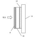
- the radio wave absorber of the present invention in one aspect thereof, further has a reflective layer.
- the conductive nonwoven fabric of the present invention has a metal layer only on one side of the nonwoven fabric, and the reflective layer is arranged on the side opposite to the metal layer.
- the electromagnetic wave absorption characteristics are more excellent.
- the incident radio wave is absorbed and attenuated in the process of passing through the conductive nonwoven fabric of the present invention, and reflected by the reflective layer.
- the reflected radio wave is further attenuated by the interference with the incident radio wave.
- the reflection of the radio wave on the incident surface is suppressed and the radio wave is not transmitted to the side opposite to the incident surface.
- the reflective layer is not particularly limited as long as it can function as a radio wave reflective layer in the radio wave absorber.
- the reflective layer is not particularly limited, but examples thereof include a metal film, a metal foil, and a conductive material.
- the metal film is not particularly limited as long as it is a layer containing a metal as a material.
- the metal film may contain a component other than a metal as long as the effect of the present invention is not significantly impaired.
- the total amount of metals in the metal film is, for example, 30% by mass or more, preferably 50% by mass or more, more preferably 75% by mass or more, even more preferably 80% by mass or more, still more preferably 90% by mass or more. , Particularly preferably 95% by mass or more, very preferably 99% by mass or more, and usually less than 100% by mass.
- the metal is not particularly limited, and examples thereof include aluminum, copper, iron, silver, gold, chromium, nickel, molybdenum, gallium, zinc, tin, niobium, indium and the like. Further, a metal compound such as ITO can also be used as a material for the metal film. These may be used alone or in combination of two or more.
- the thickness of the reflective layer is not particularly limited.
- the thickness of the reflective layer is, for example, 1 ⁇ m or more and 500 ⁇ m or less, preferably 2 ⁇ m or more and 200 ⁇ m or less, and more preferably 5 ⁇ m or more and 100 ⁇ m or less.
- the reflective layer may be composed of a single reflective layer, or may be a combination of two or more reflective layers.
- the radio wave absorber of the present invention when the radio wave absorber of the present invention has a reflection layer, the radio wave absorber of the present invention, in one aspect thereof, optionally has a dielectric layer.
- the dielectric layer is disposed between the reflective layer and the conductive nonwoven fabric of the present invention.
- the dielectric layer is not particularly limited as long as it can function as a dielectric for a target wavelength in the radio wave absorber.
- the dielectric layer is not particularly limited, but examples thereof include a resin sheet and an adhesive.
- the resin sheet is not particularly limited as long as it is a sheet-shaped material containing resin as a material.
- the resin sheet may contain components other than the resin as long as the effect of the present invention is not significantly impaired.
- the total amount of the resin in the resin sheet is, for example, 50% by mass or more, preferably 70% by mass or more, more preferably 90% by mass or more, further preferably 95% by mass or more, and usually less than 100% by mass. is there.
- the resin is not particularly limited, and examples thereof include ethylene vinyl acetate copolymer (EVA), vinyl chloride, urethane, acrylic, acryl urethane, polyolefin, polyethylene, polypropylene, silicone, polyethylene terephthalate, polyester, polystyrene, polyimide, polycarbonate, polyamide.
- EVA ethylene vinyl acetate copolymer
- vinyl chloride vinyl chloride
- urethane acrylic
- acryl urethane polyolefin
- polyethylene polypropylene
- silicone polyethylene terephthalate
- polyester polystyrene
- polyimide polyimide
- polycarbonate polyamide
- Synthetic resin such as polysulfone, polyether sulfone, epoxy, etc., and synthesis of polyisoprene rubber, polystyrene/butadiene rubber, polybutadiene rubber, chloroprene rubber, acrylonitrile/butadiene rubber, butyl rubber, acrylic rubber, ethylene/propylene rubber and silicone rubber It is preferable to use a rubber material as the resin component. These can be used alone or in combination of two or more.
- the dielectric layer may be foam or adhesive.
- the dielectric layer may be adhesive. Therefore, when a non-adhesive dielectric is laminated on another layer with an adhesive layer, a combination of the dielectric and the adhesive layer becomes a "dielectric layer".
- the dielectric layer preferably includes a pressure-sensitive adhesive layer from the viewpoint of easy lamination with an adjacent layer.
- the layer structure of the dielectric layer is not particularly limited.
- the dielectric layer may be composed of one type of dielectric layer alone, or may be a combination of two or more types of dielectric layers.
- a dielectric layer having a three-layer structure including a non-adhesive dielectric and pressure-sensitive adhesive layers arranged on both surfaces thereof, a one-layer dielectric layer including a dielectric having an adhesive property, and the like can be mentioned.
- the thickness d of the conductive nonwoven fabric of the present invention is expressed by the formula (1): ⁇ /16 ⁇ d (preferably ⁇ /16 ⁇ d ⁇ / 4, more preferably ⁇ /8 ⁇ d ⁇ /4 (where ⁇ represents the wavelength of the target radio wave). With the thickness d, the radio wave absorption characteristics are further improved.
- the total d′ of the thickness of the conductive nonwoven fabric of the present invention and the thickness of the dielectric layer is expressed by the formula (1′): ⁇ . /16 ⁇ d′ (preferably ⁇ /16 ⁇ d ⁇ /4, more preferably ⁇ /8 ⁇ d′ ⁇ /4) (where ⁇ represents the wavelength of the target radio wave).
- ⁇ represents the wavelength of the target radio wave.
- ⁇ is the wavelength of the radio wave targeted by the radio wave absorber of the present invention, and a value suitable for the application is selected.
- ⁇ is a value obtained by dividing the speed of light by the frequency, and is, for example, 0.2 cm or more and 1.5 cm or less, preferably 0.3 cm or more and 1.2 cm or less.
- Example 1 Production of conductive nonwoven fabric (Example 1) As the nonwoven fabric 1, a spunlace nonwoven fabric (material: PET) having a thickness of 500 ⁇ m and a basis weight of 90 g/m 2 was used. The non-woven fabric was placed in a vacuum device and evacuated to 5.0 ⁇ 10 ⁇ 4 Pa or less. Subsequently, a barrier layer 1 made of silicon, a metal layer made of Hastelloy, and a barrier layer 2 made of silicon are provided in this order on one surface of the nonwoven fabric by DC magnetron sputtering with an argon gas introduced to adjust the gas pressure to 0.5 Pa. The layers were laminated to obtain a conductive non-woven fabric.
- a spunlace nonwoven fabric material: PET
- the non-woven fabric was placed in a vacuum device and evacuated to 5.0 ⁇ 10 ⁇ 4 Pa or less.
- a barrier layer 1 made of silicon, a metal layer made of Hastelloy, and a barrier layer 2 made of silicon are provided in this order on one surface
- Examples 2 to 10 and Comparative Examples 1 to 8 A conductive non-woven fabric was obtained in the same manner as in Example 1 except that the kind of the non-woven fabric, the thickness of the non-woven fabric, the weight of the non-woven fabric, the amount of metal deposited, and the layer configuration of the layer formed by sputtering were changed as described in the table.
- Example 11 The non-woven fabric 10 is used, the non-woven fabric is installed in a vacuum device, and the non-woven fabric is evacuated to 5.0 ⁇ 10 ⁇ 4 Pa or less, and then argon gas is introduced to carry out sputtering at a gas pressure of 0.25 Pa.
- a conductive nonwoven fabric was obtained in the same manner as in Example 1 except that the above was changed to.
- Example 12 Use the non-woven fabric 11, install the non-woven fabric in a vacuum device, and evacuate it to a pressure of 5.0 ⁇ 10 ⁇ 4 Pa or less, and then introduce argon gas and set the gas pressure to 0.25 Pa to perform sputtering.
- a conductive nonwoven fabric was obtained in the same manner as in Example 1 except that the above was changed to.
- Example 13 The non-woven fabric is placed in a vacuum apparatus, vacuum exhaust is performed until the pressure becomes 5.0 ⁇ 10 ⁇ 4 Pa or less, and then argon gas is introduced to change the gas pressure to 0.25 Pa to perform sputtering.
- a conductive nonwoven fabric was obtained in the same manner as in Example 2.
- Non-woven fabric 1 Spunlace, material PET, unit weight 90 g/m 2 , thickness 500 ⁇ m
- Non-woven fabric 2 spun bond, material PET, basis weight 50 g/m 2 , thickness 240 ⁇ m
- Nonwoven fabric 3 melt blown, material LCP, fabric weight 6 g/m 2 , thickness 18 ⁇ m
- Nonwoven fabric 4 melt blown, material PBT, basis weight 120 g/m 2 , thickness 178 ⁇ m
- Nonwoven fabric 5 Melt blow, material PBT, basis weight 20 g/m 2 , thickness 178 ⁇ m
- Nonwoven fabric 6 melt blown, material PBT, basis weight 86 g/m 2 , thickness 75 ⁇ m
- Nonwoven fabric 7 spunlace, material PET, fabric weight 25 g/m 2 , thickness 2300 ⁇ m
- Nonwoven fabric 8 Needle punch, material acrylic, basis weight 35 g/m 2 , thickness 250 ⁇ m
- Nonwoven fabric 9 Needle punch, material PET, fabric weight 40 g/
- Pulshut (product name Pulshut, manufactured by Asahi Kasei Corporation) was used as it was. Pulshut has a basis weight of 45 g/m 2 and a thickness of 86 ⁇ m, and the surface of the conductive surface was insulated and protected by the resin sheet.
- Loss rate (Ploss/Pin) 1-(S11 2 +S21 2 )/1 Formula (2).
- the radio wave absorption was evaluated according to the following criteria based on the loss rate at each frequency. ⁇ : Loss rate 0.45 or more ⁇ : Loss rate greater than 0.40 and less than 0.45. X: Loss rate 0.40 or less.
- radio wave reflectivity The radio wave reflectivity was evaluated according to the following criteria based on S11 at each frequency. A: S11 is less than 0.16. ⁇ : S11 is 0.16 or more and 0.25 or less. X: S11 exceeds 0.25.
- the radio wave absorption amount of the obtained radio wave absorber at Ka (26.5 to 45 GHz) and W band (75 to 110 GHz) was measured based on JIS R1679.
- the radio wave absorber was set so that the radio wave incident direction was on the metal layer side.
- the loss rate was calculated from the absorption amount (dB) at each frequency and evaluated according to the following criteria.
- ⁇ Loss rate: 0.75 or more
- O Loss rate less than 0.75, 0.50 or more.
- ⁇ Loss rate: less than 0.50, 0.25 or more
- ⁇ loss rate less than 0.25.
- the gradient of metal deposition amount (the slope of the graph of high luminance area ratio and thickness) and the metal deposition range are as follows. was measured as follows. The slope of change in the high luminance area ratio was calculated by analyzing a cross-sectional image obtained by an X-ray CT apparatus. The conductive non-woven fabric was cut into about 3 mm square to make a measurement sample, and a three-dimensional image was obtained with an X-ray microscope (manufactured by Rigaku Corporation, nano3DX).
- Example 11 Shooting conditions
- Example 12 shooting conditions Number of projections: 1200 sheets Binning: 2 Exposure time: 15 seconds/sheet Spatial resolution: 2.16 ⁇ m/pixel.
- Examples 2 and 13 shooting conditions Number of projections: 1200 sheets Binning: 2 Exposure time: 40 seconds/sheet Spatial resolution: 0.54 ⁇ m/pixel.
- the obtained three-dimensional image was analyzed as follows with image analysis software Avizo9.7 (manufactured by Thermo Fisher Scientific) and image processing software Image J FIJ (December 30, 2017 version, open source software). 1) to (4) use Avizo 9.7, and (5) use Image J Fuji.
- a three-dimensional image was obtained by reconstructing a measurement image by X-ray CT as an image having a luminance value of 256 layers (8 bits).
- a slice image was formed on the xy plane with the thickness direction as the z-axis, and the image was further cut so that the bottom surface of the xy plane was a quadrangle.
- the conductive non-woven fabric portion was selected by performing binarization by the Auto threshold function (moment).
- the noise was removed by the Opening process, and the part in which the conductive nonwoven fabric was present and the part in which only air was present were separated.
- the thickness position (mm) was plotted on the X axis, and the high luminance area ratio (%) was plotted on the Y axis to prepare a graph of the high luminance area ratio and the thickness.
- the high brightness area ratio means the ratio of the high brightness area to the entire brightness area.
- Hastelloy is a composition: molybdenum 16.4% by weight, nickel 55.2% by weight, chromium 18.9% by weight, iron 5.5% by weight, tungsten 3.5% by weight, silica 0.5% by weight).
- Stainless steel is an alloy having the composition: iron 54% by weight, chromium 26% by weight, nickel 19% by weight, manganese 1% by weight.
- Monel is an alloy of composition: 65 wt% nickel, 33 wt% copper, 2 wt% iron.
Landscapes
- Engineering & Computer Science (AREA)
- Textile Engineering (AREA)
- Physics & Mathematics (AREA)
- Electromagnetism (AREA)
- Microelectronics & Electronic Packaging (AREA)
- Shielding Devices Or Components To Electric Or Magnetic Fields (AREA)
- Laminated Bodies (AREA)
- Chemical Or Physical Treatment Of Fibers (AREA)
- Non-Insulated Conductors (AREA)
Abstract
高周波に対してもより高い電波吸収特性(高吸収性、低反射性)を備える材料を 提供すること。 少なくとも一方の面に金属層を有する導電性不織布であって、シート抵抗が200~600Ω/□ であり、且つ密度が2.0×10⁴~8.0×10⁵g/m3である、導電性不織布。
Description
本発明は、導電性不織布等に関する。
従来、携帯通信機器、電子機器、家庭用電化製品では、電波の漏洩や侵入を防止するために、電波吸収材料を施した部材が用いられている。近年では、特に電波を利用した電子機器(情報通信機器)においては、他の電子機器の誤作動及び信号劣化の防止、並びに、人体への悪影響の防止の観点から、不要な電磁波を吸収する電波吸収体が広く採用されている。電波吸収体としては、各種ゴムや樹脂材料に磁性体金属粉を分散させてなるものが用いられている。また、例えば、布帛の表面上に金属が付着されたノイズ吸収布帛が報告されている(特許文献1)。
5GやIoTなど大容量・高速通信化していく中で、電子機器からのノイズは増えることが予想される。しかし、現在対策で用いられている電波吸収体は5Gやミリ波レーダーなどに利用されるレベルの高周波(例えば28GHz、39GHz、79GHzなど)に対応することが難しい。
そこで、本発明は、高周波の電波に対しても、より高い電波吸収特性(高吸収性、低反射性)を備える材料を提供することを課題とする。
本発明者は、上記課題に鑑みて鋭意研究を重ねた結果、金属層を有する導電性不織布であって、シート抵抗が200~600Ω/□であり、且つ密度が2.0×104~8.0×105g/m3である、導電性不織布であれば、上記課題を解決できることを見出した。本発明者はこの知見に基づいてさらに研究を進めた結果、本発明を完成させた。
即ち、本発明は、下記の態様を包含する。
項1. 少なくとも一方の面における金属層を有する導電性不織布であって、シート抵抗が200~600Ω/□であり、且つ密度が2.0×104~8.0×105g/m3である、導電性不織布。
項2. 金属元素及び/又は半金属元素付着量が5~150μg/cm2である、項1に記載の導電性不織布。
項3. 前記金属層の少なくとも一方の面上に、ニッケル、ケイ素、チタン、及びアルミニウムからなる群より選択される少なくとも1種の元素を含有するバリア層を有する、項1又は2に記載の導電性不織布。
項4. 前記金属層が、ニッケル、モリブデン、クロム、チタン、及びアルミニウムからなる群より選択される少なくとも1種の元素を含有する、項1~3のいずれかに記載の導電性不織布。
項5. X線CT装置により測定される高輝度面積率の変化の傾きが、-3000以上-10以下である、項1~4いずれかに記載の導電性不織布。
項6. 項1~5のいずれかに記載の導電性不織布を含む、電波吸収体。
項7. 前記導電性不織布が、更に接着剤層を備える、項6記載の電波吸収体。
項8. 前記導電性不織布の厚みdが、式(1):λ/16≦d(式中、λは対象とする電波の波長を示す。)を満たす、項6又は7に記載の電波吸収体。
項9. 前記導電性不織布と反射層を有し、前記導電性不織布のシート抵抗が200~600Ω/□である面とは他方の面に反射層を有する、項8記載の電波吸収体。
項10. 項6~9いずれか記載の電波吸収体を有する、筐体。
項11. 前記導電性不織布を前記筐体内面に有する、項10記載の筐体。
項12. 前記導電性不織布が、前記筐体の開口部に有する、項10記載の筐体。
項13. 項6~9いずれか記載の電波吸収体、又は、項10~12いずれか記載の筐体を有する、電子デバイス。
本発明によれば、高周波に対してもより高い電波吸収特性(高吸収性、低反射性)を備える材料(導電性不織布)を提供することができる。この導電性不織布を利用することにより、各種電波吸収体を提供することができる。
本明細書中において、「含有」及び「含む」なる表現については、「含有」、「含む」、「実質的にからなる」及び「のみからなる」という概念を含む。
本発明は、その一態様において、少なくとも一方の面に金属層を有する導電性不織布であって、シート抵抗が200~600Ω/□であり、且つ密度が2.0×104~8.0×105g/m3である、導電性不織布(本明細書において、「本発明の導電性不織布」と示すこともある。)に関する。以下に、これについて説明する。なお、本発明の導電性不織布においては、不織布に対して金層層側を「上」側とし、反対に不織布側を「下」側とする。
<1.不織布>
不織布は、繊維から構成されるものであれば、特に制限されない。不織布は、本発明の効果が著しく損なわれない限りにおいて、繊維以外の成分、物質等が含まれていてもよい。その場合、不織布中の繊維の合計量は、例えば80質量%以上、好ましくは90質量%以上、より好ましくは95質量%以上、さらに好ましくは99質量%以上であり、通常100質量%未満である。
不織布は、繊維から構成されるものであれば、特に制限されない。不織布は、本発明の効果が著しく損なわれない限りにおいて、繊維以外の成分、物質等が含まれていてもよい。その場合、不織布中の繊維の合計量は、例えば80質量%以上、好ましくは90質量%以上、より好ましくは95質量%以上、さらに好ましくは99質量%以上であり、通常100質量%未満である。
不織布の層構成は特に制限されない。不織布は、1種単独の不織布から構成されるものであってもよいし、2種以上の不織布が複数組み合わされたものであってもよい。
繊維を構成する素材は、繊維状である又は繊維状に成形可能な素材である限り、特に制限されない。繊維の素材としては、例えばポリエチレンテレフタレート(PET)、ポリブチレンテレフタレート(PBT)、ポリエチレンナフタレート、変性ポリエステル等のポリエステル系樹脂、ポリエチレン(PE)樹脂、ポリプロピレン(PP)樹脂、ポリスチレン樹脂、環状オレフィン系樹脂等のポリオレフィン類樹脂、ポリ塩化ビニル、ポリ塩化ビニリデン等のビニル系樹脂、ポリビニルブチラール(PVB)等のポリビニルアセタール樹脂、ポリエーテルエーテルケトン(PEEK)樹脂、ポリサルホン(PSF)樹脂、ポリエーテルサルホン(PES)樹脂、ポリカーボネート(PC)樹脂、ポリアミド樹脂、ポリイミド樹脂、アクリル樹脂、トリアセチルセルロース(TAC)樹脂等の合成樹脂、天然樹脂、セルロース、ガラス等が挙げられる。繊維は、1種単独の繊維素材から構成されるものであってもよいし、2種以上の繊維素材が複数組み合わされたものであってもよい。
不織布の目付(坪量)は、例えば1~500g/m2、好ましくは3~300g/m2、より好ましくは5~150g/m2である。
不織布の厚みは、例えば1~3000μm、好ましくは5~1500μm、より好ましくは10~800μmである。
不織布の密度の下限は、好ましくは2.0×10⁴g/m3であり、より好ましくは1.0×105g/m3であり、さらに好ましくは1.5×105g/m3である。不織布の密度の上限は好ましくは8.0×105g/m3であり、より好ましくは6.0×105g/m3である。
前記不織布の密度であることで、本発明の導電性不織布の密度を上記範囲に調整しやすくなる。この結果、導電性不織布の電波吸収性が向上する。
前記不織布の密度であることで、本発明の導電性不織布の密度を上記範囲に調整しやすくなる。この結果、導電性不織布の電波吸収性が向上する。
この理由については、特定の理論に束縛されないが、特定範囲の密度の不織布を用いることで、金属が不織布表面にのみ付着するのではなく、不織布内部にまで入り込むため、電波吸収特性(特に吸収性)が向上すると考えられる。
<2.金属層>
金属層は、不織布上に配置される、換言すれば不織布の有する2つの主面の少なくとも1方の表面上に配置される。
金属層は、不織布上に配置される、換言すれば不織布の有する2つの主面の少なくとも1方の表面上に配置される。
金属層は、金属を素材として含む層である限り、特に制限されない。金属層は、本発明の効果が著しく損なわれない限りにおいて、金属以外の成分が含まれていてもよい。その場合、金属層中の金属量は、例えば80質量%以上、好ましくは90質量%以上、より好ましくは95質量%以上、さらに好ましくは99質量%以上であり、通常100質量%未満である。
金属層を構成する金属としては、電波吸収特性を発揮できるものであれば特に制限されない。金属としては、例えばニッケル、モリブデン、クロム、チタン、アルミニウム、金、銀、銅、亜鉛、スズ、白金、鉄、インジウム、これらの金属を含む合金、及び、これらの金属又はこれらの金属を含む合金の金属化合物等が挙げられる。金属層は、導電性不織布の電波吸収特性の経時変化を抑制する(耐久性の)観点から、ニッケル、モリブデン、クロム、チタン、及びアルミニウムからなる群より選択される少なくとも1種の金属元素を含有することが好ましい。
上記ニッケル、モリブデン、クロム、チタン、及びアルミニウムからなる群より選択される少なくとも1種の金属元素を含有する場合、その含有量は、例えば10質量%以上、好ましくは20質量%以上、より好ましくは40質量%以上、さらに好ましくは60質量%以上であり、通常100質量%未満である。
金属層としては、耐久性、シート抵抗の調整が容易である観点から、モリブデンを含有する金属層が好ましく用いられる。モリブデンの含有量の下限は特に限定されないが、より耐久性を高める観点から、5重量%が好ましく、7重量%がより好ましく、9重量%が更に好ましく、11重量%がより更に好ましく、13重量%が特に好ましく、15重量%が非常に好ましく、16重量%が最も好ましい。また、上記モリブデンの含有量の上限は、表面抵抗値の調整の容易化の観点から、70重量%が好ましく、30重量%がより好ましく、25重量%がさらに好ましく、20重量%が更に好ましい。
金属層は、モリブデンを含有している場合、さらにニッケル及びクロムを含有することがより好ましい。金属層にモリブデンに加えてニッケル及びクロムを含有することでより耐久性に優れた導電性不織布とすることができる。ニッケル、クロム及びモリブデンを含有する合金としては、例えば、ハステロイB-2、B-3、C-4、C-2000、C-22、C-276、G-30、N、W、X等の各種グレードが挙げられる。
金属層がモリブデン、ニッケル及びクロムを含有する場合、モリブデンの含有量が5重量%以上、ニッケルの含有量が40重量%以上、クロムの含有量が1重量%以上であることが好ましい。モリブデン、ニッケル及びクロムの含有量が上記範囲であることで、より耐久性に優れた導電性不織布とすることができる。上記モリブデン、ニッケル及びクロムの含有量は、モリブデン含有量が7重量%以上、ニッケル含有量が45重量%以上、クロム含有量が3重量%以上であることがより好ましい。上記モリブデン、ニッケル及びクロムの含有量は、モリブデン含有量が9重量%以上、ニッケル含有量が47重量%以上、クロム含有量が5重量%以上であることが更に好ましい。上記モリブデン、ニッケル及びクロムの含有量は、モリブデン含有量が11重量%以上、ニッケル含有量が50重量%以上、クロム含有量が10重量%以上であることがより更に好ましい。上記モリブデン、ニッケル及びクロムの含有量は、モリブデン含有量が13重量%以上、ニッケル含有量が53重量%以上、クロム含有量が12重量%以上であることが特に好ましい。上記モリブデン、ニッケル及びクロムの含有量は、モリブデン含有量が15重量%以上、ニッケル含有量が55重量%以上、クロム含有量が15重量%以上であることが非常に好ましい。上記モリブデン、ニッケル及びクロムの含有量は、モリブデン含有量が16重量%以上、ニッケル含有量が57重量%以上、クロム含有量が16重量%以上であることが最も好ましい。また、上記ニッケルの含有量は、80重量%以下であることが好ましく、70重量%以下であることがより好ましく、65重量%以下であることが更に好ましい。上記クロム含有量の上限は、50重量%以下であることが好ましく、40重量%以下であることがより好ましく、35重量%以下であることが更に好ましい。
金属層は、上記モリブデン、ニッケル及びクロム以外の金属を含有してもよい。そのような金属としては、例えば、鉄、コバルト、タングステン、マンガン、チタン等が挙げられる。金属層がモリブデン、ニッケル及びクロムを含有する場合、上記モリブデン、ニッケル及びクロム以外の金属の合計含有量の上限は、金属層の耐久性の観点から、好ましくは45重量%、より好ましくは40重量%、更に好ましくは35重量%、より更に好ましくは30重量%、特に好ましくは25重量%、非常に好ましくは23重量%である。上記モリブデン、ニッケル及びクロム以外の金属の合計含有量の下限は、例えば1重量%以上である。
金属層が鉄を含有する場合、金属層の耐久性の観点から、含有量の好ましい上限は25重量%、より好ましい上限は20重量%、更に好ましい上限は15重量%であり、好ましい下限は1重量%である。金属層がコバルト及び/又はマンガンを含有する場合、金属層の耐久性の観点から、それぞれ独立して、含有量の好ましい上限は5重量%、より好ましい上限は4重量%、更に好ましい上限は3重量%であり、好ましい下限は0.1重量%である。上記金属層がタングステンを含有する場合、金属層の耐久性の観点から、含有量の好ましい上限は8重量%、より好ましい上限は6重量%、更に好ましい上限は4重量%であり、好ましい下限は1重量%である。
金属層は、ケイ素及び/又は炭素を含有してもよい。金属層がケイ素及び/又は炭素を含有する場合、上記ケイ素及び/又は炭素の含有量は、それぞれ独立して、1重量%以下であることが好ましく0.5重量%以下であることがより好ましい。また、金属層がケイ素及び/又は炭素を含有する場合、上記ケイ素及び/又は炭素の含有量は、0.01重量%以上であることが好ましい。
金属層に由来する金属元素及び/又は半金属元素付着量は、後述のシート抵抗を満たし得るものである限り特に制限されない。金属層に由来する金属元素及び/又は半金属元素付着量は、例えば5~150μg/cm2、好ましくは10~100μg/cm2、より好ましくは20~50μg/cm2である。
金属層に由来する金属元素及び/又は半金属元素付着量は、蛍光X線分析により求めることができる。具体的には、走査型蛍光X線分析装置(例えば、リガク社製走査型蛍光X線分析装置 ZSX PrimusIII+もしくは、同等品)を用いて加速電圧は50kV、加速電流は50mA、積分時間は60秒として分析する。測定対象の成分のKα線のX線強度を測定し、ピーク位置に加えてバックグラウンド位置での強度も測定し、正味の強度が算出できるようにする。あらかじめ作成した検量線から、測定した強度値を付着量に換算することができる。同一のサンプルに5回分析を行い、その平均値を平均付着量とする。
金属層の層構成は特に制限されない。金属層は、1種単独の金属層から構成されるものであってもよいし、2種以上の金属層が複数組み合わされたものであってもよい。
<3.バリア層>
本発明の導電性不織布は、金属層の少なくとも一方の面上(好ましくは両面上)にバリア層を有することが好ましい。
本発明の導電性不織布は、金属層の少なくとも一方の面上(好ましくは両面上)にバリア層を有することが好ましい。
バリア層は、金属層を保護し、その劣化を抑えることができる層である限り、特に制限されないが、金属層とは異なる組成であることが好ましい。バリア層の素材としては、例えば金属、半金属、合金、金属化合物、半金属化合物等が挙げられる。バリア層は、本発明の効果が著しく損なわれない限りにおいて、上記素材以外の成分が含まれていてもよい。その場合、バリア層中の上記素材量は、例えば80質量%以上、好ましくは90質量%以上、より好ましくは95質量%以上、さらに好ましくは99質量%以上であり、通常100質量%未満である。
バリア層に好適に用いられる金属としては、例えばニッケル、チタン、アルミニウム、ニオブ、コバルト等が挙げられる。バリア層に好適に用いられる半金属としては、例えばケイ素、ゲルマニウム、アンチモン、ビスマス等が挙げられる。
バリア層に用いられる金属化合物及び半金属化合物の具体例としては、SiO2、SiOx(Xは酸化数を表し、0<X<2)、Al2O3、MgAl2O4、CuO、CuN、TiO2、TiN、AZO(アルミニウムドープ酸化亜鉛)等が挙げられる。
バリア層は、好ましくはニッケル、ケイ素、チタン、及びアルミニウムからなる群より選択される少なくとも1種の元素を含有する。これらの中でも、好ましくはケイ素が挙げられる。
バリア層に由来する金属元素及び/又は半金属元素付着量は、後述のシート抵抗を満たし得るものである限り特に制限されない。バリア層に由来する金属元素及び/又は半金属元素付着量は、例えば2~15μg/cm2、好ましくは4~12μg/cm2、より好ましくは6~10μg/cm2である
バリア層の層構成は特に制限されない。バリア層は、1種単独のバリア層から構成されるものであってもよいし、2種以上のバリア層が複数組み合わされたものであってもよい。
バリア層の層構成は特に制限されない。バリア層は、1種単独のバリア層から構成されるものであってもよいし、2種以上のバリア層が複数組み合わされたものであってもよい。
<4.特性>
本発明の導電性不織布は、少なくとも一方の面におけるシート抵抗が200~600Ω/□であり、且つ密度が2.0×104~8.0×105g/m3である。このような特性を備えることによって、表面においてより高い電波透過性を発揮しつつ、内部で電波を吸収することができ、高周波に対してもより高い電波吸収特性(高吸収性、低反射性)を発揮することができる。
本発明の導電性不織布は、少なくとも一方の面におけるシート抵抗が200~600Ω/□であり、且つ密度が2.0×104~8.0×105g/m3である。このような特性を備えることによって、表面においてより高い電波透過性を発揮しつつ、内部で電波を吸収することができ、高周波に対してもより高い電波吸収特性(高吸収性、低反射性)を発揮することができる。
シート抵抗は、本発明の導電性不織布の金属層側の表面上の表面抵抗値であり、表面抵
抗計(例えば、MITUBISHI CHEMICAL ANALYTECH社製(商品
名:Loresta-EP)、又はその同等品)を用いて4端子法によって測定することができる。測定にはESPプローブ(MCP-TP08P又はその同等品)を使用し、試料に対してプローブの全てのピンが均一になるように押し当てて測定を行う。シート抵抗の下限値は、200Ω/□であり、好ましくは250Ω/□、より好ましくは300Ω/□、さらに好ましくは320Ω/□である。シート抵抗の上限値は、600Ω/□であり、好ましくは500Ω/□であり、より好ましくは450Ω/□である。上記シート抵抗の範囲であることで、電波吸収特性(特に低反射性)が一層向上する。
抗計(例えば、MITUBISHI CHEMICAL ANALYTECH社製(商品
名:Loresta-EP)、又はその同等品)を用いて4端子法によって測定することができる。測定にはESPプローブ(MCP-TP08P又はその同等品)を使用し、試料に対してプローブの全てのピンが均一になるように押し当てて測定を行う。シート抵抗の下限値は、200Ω/□であり、好ましくは250Ω/□、より好ましくは300Ω/□、さらに好ましくは320Ω/□である。シート抵抗の上限値は、600Ω/□であり、好ましくは500Ω/□であり、より好ましくは450Ω/□である。上記シート抵抗の範囲であることで、電波吸収特性(特に低反射性)が一層向上する。
また上記シート抵抗は、導電性不織布の金属層側の表面に樹脂シート等の絶縁保護が施されている場合には、非接触式抵抗測定器(ナプソン株式会社製、商品名:EC-80P、又はその同等品)を用いて渦電流法によって測定することができる。
密度は、本発明の導電性不織布の密度であり、JIS L 1913:2010に規定の方法に従い測定して得られた試料の厚さを厚み、単位面積当たりの質量を目付とし、次の(1)式から密度を算出することができる。
密度(g/m3)=目付(g/m2)/厚み(m) 式(1)
なお、試料から必要な大きさの試験片が採取できない場合、厚みは試料に対して0.5kPaの荷重を掛けて測定した値を厚みとすることができる。本発明の導電性不織布の密度は、2.0×10⁴~8.0×10⁵g/m3である。本発明の導電性不織布の密度の下限は、好ましくは1.0×105g/m3であり、より好ましくは1.5×105g/m3であり、さらに好ましくは2.0×105g/m3である。本発明の導電性不織布の密度の上限は好ましくは6.0×105g/m3であり、より好ましくは4.0×105g/m3である。上記導電性不織布の密度であることで、電波吸収特性(特に高吸収性)が一層向上する。
密度(g/m3)=目付(g/m2)/厚み(m) 式(1)
なお、試料から必要な大きさの試験片が採取できない場合、厚みは試料に対して0.5kPaの荷重を掛けて測定した値を厚みとすることができる。本発明の導電性不織布の密度は、2.0×10⁴~8.0×10⁵g/m3である。本発明の導電性不織布の密度の下限は、好ましくは1.0×105g/m3であり、より好ましくは1.5×105g/m3であり、さらに好ましくは2.0×105g/m3である。本発明の導電性不織布の密度の上限は好ましくは6.0×105g/m3であり、より好ましくは4.0×105g/m3である。上記導電性不織布の密度であることで、電波吸収特性(特に高吸収性)が一層向上する。
本発明の導電性不織布は、不織布に、金属層を構成する元素(必要に応じてバリア層を構成する元素も)を付着して得ることができる。この元素の付着量(金属元素及び/又は半金属元素付着量)は、電波吸収特性の観点から、好ましくは5~150μg/cm2である。より好ましくは15~100μg/cm2であり、さらに好ましくは30~60μg/cm2である。
本発明の導電性不織布は、表面(シート抵抗が200~600Ω/□である面)とその内部とにおいて金属付着量の勾配を有することが好ましい。金属付着量の勾配を有することで、電波吸収特性(特に高吸収性)が一層向上する。この理由は特定の理論に束縛されないが、金属付着量の勾配を有することで、外部から進入した電波が、金属付着量の多い表面で捕捉される。この時シート抵抗が特定の値であることで電波の反射が抑制される。
入射した電波は、本発明の導電性不織布を通過する過程で電流に変換され、吸収・減衰される。本発明の導電性不織布の内部では表面に比べ金属付着量が少なく、すなわち、電気抵抗値が大きくなる。これにより、導電性不織布内において多重反射が生じ、吸収・減衰が一層生じやすくなることが考えられる。
金属付着量の勾配は、不織布の密度、金属付着量の調整や、付着方法の調整(例えば、後述のスパッタ法の調整)等により調整することができる。
金属付着量の勾配は、X線CT装置による撮影により確認することができる。金属が付着している領域はX線吸収量が導電性不織布を構成する繊維単体に比べて大きいため、高輝度の領域として撮影像が得られる。
入射した電波は、本発明の導電性不織布を通過する過程で電流に変換され、吸収・減衰される。本発明の導電性不織布の内部では表面に比べ金属付着量が少なく、すなわち、電気抵抗値が大きくなる。これにより、導電性不織布内において多重反射が生じ、吸収・減衰が一層生じやすくなることが考えられる。
金属付着量の勾配は、不織布の密度、金属付着量の調整や、付着方法の調整(例えば、後述のスパッタ法の調整)等により調整することができる。
金属付着量の勾配は、X線CT装置による撮影により確認することができる。金属が付着している領域はX線吸収量が導電性不織布を構成する繊維単体に比べて大きいため、高輝度の領域として撮影像が得られる。
導電性不織布の表面(シート抵抗が200~600Ω/□である面)とその内部とにおける金属付着量の勾配は、X線CT装置により測定される金属分布の変化の傾きが、-10以下であることが好ましく、-15以下であることがより好ましく、-18以下であることがさらに好ましい。高輝度面積率の変化の傾きは-3000以上であることが好ましく、-2500以上であることがより好ましく、-2375以上であることがさらに好ましく、-1800以上であることがさらにより好ましく、-1523以上であることが特に好ましい。
上記の金属分布であることで、導電性不織布の表面から内部にかけて生じる勾配が、導電性不織布の内部の深くまで形成される。このため、電波吸収特性(特に高吸収性)が一層向上する。
金属分布の変化の傾きは、後述するX線CT装置による解析により、厚み位置をX軸(mm)、高輝度面積率((高輝度面積数/全輝度面積数)×100(%))をY軸としてプロットすることで算出される、高輝度面積率と厚みのグラフの傾きを意味する。
上記の金属分布であることで、導電性不織布の表面から内部にかけて生じる勾配が、導電性不織布の内部の深くまで形成される。このため、電波吸収特性(特に高吸収性)が一層向上する。
金属分布の変化の傾きは、後述するX線CT装置による解析により、厚み位置をX軸(mm)、高輝度面積率((高輝度面積数/全輝度面積数)×100(%))をY軸としてプロットすることで算出される、高輝度面積率と厚みのグラフの傾きを意味する。
傾きの算出はX線CT装置により得られる断面像の解析により求める。具体的には次の通りである。導電性不織布を約3mm角にカットして測定用サンプルとする。X線顕微鏡(株式会社リガク製 nano3DX又はその同等品)により測定用サンプルを測定し、3次元画像を取得する。ビニング2、露光時間は測定機の推奨時間内にて設定し、撮影枚数1200枚の条件で撮影を行う。X線源としては、金属層の金属を検出することができる線源、例えばMoやW等を用いることができる。レンズは導電性不織布を構成する繊維の繊維径を確認可能な画素数となるレンズを使用する。なお導電性不織布の厚みが、レンズの視野を超える場合、複数の画像を撮影し、画像解析ソフトにて合成し解析に用いる。得られた3次元画像を画像解析ソフトウェアAvizo9.7(Thermo Fisher Scientific社製)及び画像処理ソフトImage J Fiji(2017年12月30日バージョン、オープンソースソフトウェア:Schindelin, J.;Arganda-Carreras, I. & Frise, E. et al. (2012), “Fiji: an open-source platform for biological-image analysis”, Nature methods 9(7): 676-682)にて解析する。
解析は例えば以下のように行う事ができる。なお(1)~(4)はAvizo9.7を、(5)はImage J Fijiを使用する。
(1)X線CTによる測定画像を256階層(8bit)の輝度値を持つ画像とし、再構築して3次元画像を得る。
(2)厚み方向をz軸として、導電性不織布のシート抵抗が200~600Ω/□である面側から順にx-y平面でのスライス画像を形成する。さらにx-y平面の底面が四角形になるよう画像をカットする。
(3)Auto threshold機能により二値化を行い、導電性不織布部分を選択する。次いでOpening処理によりノイズを除去し、導電性不織布が存在する部分と空気のみが存在する部分とを分ける。
(4)マスク処理により、導電性不織布が存在する部分のみを抽出し、それ以外の部分の輝度値を0となるように調整する。
(5)画像処理ソフトにて、スライス画像ごとに、輝度値が1以上の画素のカウント数(全輝度面積数)及び輝度値が閾値以上の画素のカウント数(高輝度面積数)を取得する。なお、導電性不織布の下側の面から導電性不織布厚みの5%の範囲までにおける輝度値の最大値の平均値を閾値とする。輝度値0の領域は空気層とみなし、以後の解析では用いない。
(6)厚み位置をX軸(mm)、高輝度面積率((高輝度面積数/全輝度面積数)×100(%))をY軸としてプロットし、高輝度面積率と厚みのグラフを作成する。
(1)X線CTによる測定画像を256階層(8bit)の輝度値を持つ画像とし、再構築して3次元画像を得る。
(2)厚み方向をz軸として、導電性不織布のシート抵抗が200~600Ω/□である面側から順にx-y平面でのスライス画像を形成する。さらにx-y平面の底面が四角形になるよう画像をカットする。
(3)Auto threshold機能により二値化を行い、導電性不織布部分を選択する。次いでOpening処理によりノイズを除去し、導電性不織布が存在する部分と空気のみが存在する部分とを分ける。
(4)マスク処理により、導電性不織布が存在する部分のみを抽出し、それ以外の部分の輝度値を0となるように調整する。
(5)画像処理ソフトにて、スライス画像ごとに、輝度値が1以上の画素のカウント数(全輝度面積数)及び輝度値が閾値以上の画素のカウント数(高輝度面積数)を取得する。なお、導電性不織布の下側の面から導電性不織布厚みの5%の範囲までにおける輝度値の最大値の平均値を閾値とする。輝度値0の領域は空気層とみなし、以後の解析では用いない。
(6)厚み位置をX軸(mm)、高輝度面積率((高輝度面積数/全輝度面積数)×100(%))をY軸としてプロットし、高輝度面積率と厚みのグラフを作成する。
金属分布の変化の傾き(高輝度面積率と厚みのグラフの傾き)は、高輝度面積率の最大値の点と、最大値の点よりも大きい厚み位置における、高輝度面積率の最大値の10%の値となる点との2点間における傾きを求めることで算出できる。
なお、高輝度面積率の最大値の点が複数ある場合は、導電性不織布の金属層を有する表面に近い点における値を用いる。
また高輝度面積率の最大値の10%の値となる点がない場合、導電性不織布が存在する厚み領域における最小値となる点を用いる。高輝度面積率の最小値が複数ある場合は、最大値の点よりも大きい厚み位置であり、かつ、厚み位置がより小さい点における値を用いる。
なお、導電性不織布が存在する厚み領域とは、全輝度面積数の値が最大値の20%となる最初の点の厚み位置から、全輝度面積数の値が最大値の20%となる最後の点の厚み位置までの区間を意味する。
なお、高輝度面積率の最大値の点が複数ある場合は、導電性不織布の金属層を有する表面に近い点における値を用いる。
また高輝度面積率の最大値の10%の値となる点がない場合、導電性不織布が存在する厚み領域における最小値となる点を用いる。高輝度面積率の最小値が複数ある場合は、最大値の点よりも大きい厚み位置であり、かつ、厚み位置がより小さい点における値を用いる。
なお、導電性不織布が存在する厚み領域とは、全輝度面積数の値が最大値の20%となる最初の点の厚み位置から、全輝度面積数の値が最大値の20%となる最後の点の厚み位置までの区間を意味する。
導電性不織布は、高輝度面積率と厚みのグラフにおいて、高輝度面積率の最大値の点よりも大きい厚み位置に、高輝度面積率の最大値の50%以下となる点を有することが好ましい。
高輝度面積率の最大値の50%以下となる点を有することで、導電性不織布内の抵抗値が十分大きくなる。これにより、導電性不織布内において多重反射が生じ、吸収・減衰が一層生じやすくなることが考えられる。
導電性不織布は、高輝度面積率の最大値の30%以下となる点を有することがより好ましく、20%以下となる点を有することが更に好ましく、10%以下となる点を有することがさらにより好ましい。
高輝度面積率の最大値の50%以下となる点を有することで、導電性不織布内の抵抗値が十分大きくなる。これにより、導電性不織布内において多重反射が生じ、吸収・減衰が一層生じやすくなることが考えられる。
導電性不織布は、高輝度面積率の最大値の30%以下となる点を有することがより好ましく、20%以下となる点を有することが更に好ましく、10%以下となる点を有することがさらにより好ましい。
導電性不織布の表面からの金属付着範囲は、高輝度面積率と厚みのグラフにおいて、導電性不織布の金属層を有する表面から5μm以上の厚み範囲まで存在することが好ましい。これにより、金属付着量の勾配が、導電性不織布の内部の深くまで形成される。このため、電波吸収特性(特に高吸収性)が一層向上する。金属分布は、導電性不織布の表面から10μm以上まで存在することがより好ましく、15μm以上まで存在することが更に好ましく、20μm以上まで存在することが更により好ましい。上記金属分布の存在範囲の上限は特に限定されないが、例えば導電性不織布の厚み以下、導電性不織布の厚みの90%以下、80%以下、70%以下、60%以下である。
なお、導電性不織布の表面からの金属付着範囲は、高輝度面積率と厚みのグラフにおいて導電性不織布の金属層を有する表面の厚み位置から、高輝度面積率の最大値の点よりも大きい厚み位置における高輝度面積率の最大値の10%の値となる点の厚み位置までの区間を意味する。なお高輝度面積率の最大値の10%の値となる点が存在しない場合、導電性不織布が存在する厚み領域における高輝度面積率の最小値の点までの区間を用いる。
<5.製造方法>
本発明の導電性不織布は、不織布の表面に金属を付着させる工程を含む方法により得ることができる。金属層の他に他の層(例えばバリア層等)を有する場合は、さらに、不織布の表面、金属層の表面等に他の層の構成元素を付着させる工程を含む方法により、得ることができる。
本発明の導電性不織布は、不織布の表面に金属を付着させる工程を含む方法により得ることができる。金属層の他に他の層(例えばバリア層等)を有する場合は、さらに、不織布の表面、金属層の表面等に他の層の構成元素を付着させる工程を含む方法により、得ることができる。
特に限定されないが、前記付着は、例えば、スパッタリング法、真空蒸着法、イオンプレーティング法、化学蒸着法、パルスレーザーデポジション法等により行うことができる。これらの中でも、膜厚制御性、電波吸収特性等の観点から、スパッタリング法が好ましい。
スパッタリング法としては、特に限定されないが、例えば、直流マグネトロンスパッタ、高周波マグネトロンスパッタ及びイオンビームスパッタ等が挙げられる。また、スパッタ装置は、バッチ方式であってもロール・ツー・ロール方式であってもよい。
スパッタリング法により付着する場合、表面とその内部とにおける金属付着量の勾配は、スパッタ時のガス圧により調整することもできる。スパッタ時のガス圧を下げることで、不織布の内部、より深くまで金属を付着させることができ、緩やかな勾配で分布させることができる。
<6.用途>
本発明の導電性不織布は、高周波の電波に対してもより高い電波吸収特性(高吸収性、低反射性)を備えるので、電波吸収体として好適に利用することができる。この観点から、本発明は、その一態様において、本発明の導電性不織布を含む、電波吸収体(本明細書において、「本発明の電波吸収体」と示すこともある。)に関する。
本発明の電波吸収体は、導電性不織布のシート抵抗が200~600Ω/□である面を電波の入射面に向けて、配置することが好ましい。
本発明の導電性不織布は、高周波の電波に対してもより高い電波吸収特性(高吸収性、低反射性)を備えるので、電波吸収体として好適に利用することができる。この観点から、本発明は、その一態様において、本発明の導電性不織布を含む、電波吸収体(本明細書において、「本発明の電波吸収体」と示すこともある。)に関する。
本発明の電波吸収体は、導電性不織布のシート抵抗が200~600Ω/□である面を電波の入射面に向けて、配置することが好ましい。
本発明の電波吸収体は、その一態様において、不要な電磁波を吸収する性能を有するため、例えば、光トランシーバや、次世代移動通信システム(5G)における電波対策部材として好適に利用できる。また、その他の用途として自動車、道路、人の相互間で情報通信を行う高度道路交通システム(ITS)や自動車衝突防止システムに用いるミリ波レーダーにおいても、電波干渉抑制やノイズ低減の目的で用いることができる。本発明の電波吸収体が対象とする電波の周波数は、例えば20GHz以上150GHz以下、好ましくは25GHz以上85GHz以下である。
本発明の電波吸収体は、その一態様において、本発明の導電性不織布と接着剤層を有する。接着剤層を有することで、本発明の電波吸収体を成形品や筐体等の物品に容易に取り付けることができる。例えば、導電性不織布の金属層側に接着剤層を有してもよく、金属層ではない面に接着剤層を有してもよい。接着剤層としては、公知の接着剤、感圧接着剤(粘着剤)等を用いることができる。
本発明の電波吸収体は、その一態様において、電波吸収対象物の周囲を覆うことにより使用することができる。このため、対象物の形状に応じて、適宜成形される。成形されたものを、本明細書においては、「電波吸収成形体」と表す。
電波吸収対象物としては特に限定されない。電波吸収対象物としては例えば、LSI等の電子部品、ガラスエポキシ基盤及びFPC等の回路表面又はその裏面、部品間の接続ケーブル及びコネクター部、電子部品・装置を入れる筐体、保持体等の裏又は表、電源線、伝送線等のケーブル等が挙げられる。
周囲を覆う方法は特に限定されず、巻き付け、貼付などが挙げられる。
本発明の電波吸収体は、その一態様において、接着剤等を介して筐体に貼付することにより、優れた電波吸収性を有する筐体を得ることができる。本発明の導電性不織布を有する筐体もまた、本発明の1つである。
本発明の電波吸収体は、その一態様において、接着剤等を介して電子デバイス等を内蔵する筐体の内面(より好ましくは内壁)に貼付することにより、優れた電波吸収性を有する筐体を得ることができる。
本発明の電波吸収体は、電波ノイズの発生源から離れた位置に配置し、電波吸収対象物の周囲を覆うように用いられることで、不要な電波ノイズを吸収する性能をより効果的に発揮することができる。また、電波ノイズの発生源から離れた位置に配置することで、LSI等から発生する熱の放熱を妨げにくくなる。本発明の電波吸収体は電波吸収性の観点から、電波ノイズの発生源からλ/2π以上離れた位置に配置することが好ましい。なお、λは対象とする電波の波長を示す。また、筐体内部で電波ノイズが生じた場合、空洞共振現象により筐体自身も電波ノイズ源になりうる。本発明の電波吸収体を筐体内壁に配置することで、空洞共振現象を抑制し、筐体からのノイズ発生を抑制することもできる。
発明の導電性不織布を筐体内面に有する筐体、及び、該筐体を有する電子デバイスもまた、本発明の1つである。
本発明の電波吸収体は、電波ノイズの発生源から離れた位置に配置し、電波吸収対象物の周囲を覆うように用いられることで、不要な電波ノイズを吸収する性能をより効果的に発揮することができる。また、電波ノイズの発生源から離れた位置に配置することで、LSI等から発生する熱の放熱を妨げにくくなる。本発明の電波吸収体は電波吸収性の観点から、電波ノイズの発生源からλ/2π以上離れた位置に配置することが好ましい。なお、λは対象とする電波の波長を示す。また、筐体内部で電波ノイズが生じた場合、空洞共振現象により筐体自身も電波ノイズ源になりうる。本発明の電波吸収体を筐体内壁に配置することで、空洞共振現象を抑制し、筐体からのノイズ発生を抑制することもできる。
発明の導電性不織布を筐体内面に有する筐体、及び、該筐体を有する電子デバイスもまた、本発明の1つである。
本発明の電波吸収体は、その一態様において、電子デバイス等を内蔵する筐体が開口部を有する場合、その開口部に貼付することにより、優れた電波吸収性を有する筐体を得ることができる。電子デバイス等を内蔵する筐体が開口部を有する場合、内部の電子デバイスから発生した電波ノイズが開口部から漏れ出たり、開口部がアンテナとして機能し電波ノイズを再放射したりする場合がある。このような場合に、筐体の開口部に本発明の電波吸収体を配置することで、筐体から発するノイズを低減することができる。
本発明の導電性不織布を筐体の開口部に有する筐体、及び、該筐体を有する電子デバイスもまた、本発明の1つである。
本発明の導電性不織布を筐体の開口部に有する筐体、及び、該筐体を有する電子デバイスもまた、本発明の1つである。
本発明の電波吸収成形体は、その一態様において、非導電性材料をさらに含む。該非導電性材料を含むことにより、電波吸収成形体の形状保持性を高めることができる。
本発明の電波吸収体は、接着剤等を介して種々の非導電性材料からなる部材に貼付することにより、優れた電波吸収性を有する電波吸収成形体を得ることができる。なかでも、電子デバイスを内蔵するための筐体の表面に貼着して電波吸収を付与する用途に好適である。非導電性材料からなる部材の表面に、本発明の電波吸収体が貼付されている電波吸収成形体もまた、本発明の1つである。非導電性材料からなる部材の表面に本発明の電波吸収体が貼付された筐体に、電子デバイスが内蔵されている電子デバイスもまた、本発明の1つである。
本発明の電波吸収体を、非導電性材料からなる部材の表面に貼付するだけでなく、非導電性材料からなる部材の内部に保持することによっても、優れた電波吸収性を有する電波吸収成形体を得ることができる。非導電性材料からなる部材の内部に、本発明の電波吸収体が保持されている電波吸収成形体もまた、本発明の1つである。非導電性材料からなる部材の内部に本発明の電波吸収体が保持された筐体に、電子デバイスが内蔵されている電子デバイスもまた、本発明の1つである。
本発明の電波吸収体は、その一態様において、さらに反射層を有する。反射層を有する場合、本発明の導電性不織布は不織布の片面側にのみ金属層を有し、反射層は金属層とは反対側に配置される。上記構成を有する場合、電波吸収特性がより優れる。
この理由は特定の理論に束縛されないが、入射した電波は、本発明の導電性不織布を通過する過程で吸収・減衰され、反射層にて反射される。反射された電波は、入射する電波との干渉によりさらに減衰する。この結果、入射面への電波の反射は抑制され、入射面とは逆側へは電波が透過しないことが考えられる。
反射層は、電波吸収体において電波の反射層として機能し得るものである限り、特に制限されない。反射層としては、特に制限されないが、例えば金属膜、金属箔、導電性材料等が挙げられる。
金属膜は、金属を素材として含む層である限り、特に制限されない。金属膜は、本発明の効果が著しく損なわれない限りにおいて、金属以外の成分が含まれていてもよい。その場合、金属膜中の金属の合計量は、例えば30質量%以上、好ましくは50質量%以上、より好ましくは75質量%以上、さらに好ましくは80質量%以上、さらにより好ましくは90質量%以上、特に好ましくは95質量%以上、非常に好ましくは99質量%以上であり、通常100質量%未満である。
金属としては、特に制限されず、例えばアルミニウム、銅、鉄、銀、金、クロム、ニッケル、モリブデン、ガリウム、亜鉛、スズ、ニオブ、インジウム等が挙げられる。また、金属化合物、例えばITO等も、金属膜の素材として使用することができる。これらは1種単独であってもよいし、2種以上の組み合わせであってもよい。
反射層の厚みは、特に制限されない。反射層の厚みは、例えば1μm以上500μm以下、好ましくは2μm以上200μm以下、より好ましくは5μm以上100μm以下である。
反射層の層構成は特に制限されない。反射層は、1種単独の反射層から構成されるものであってもよいし、2種以上の反射層が複数組み合わされたものであってもよい。
本発明の電波吸収体が反射層を有する場合、本発明の電波吸収体は、その一態様において、任意に誘電体層を有する。誘電体層は、反射層と、本発明の導電性不織布の間に配置される。
誘電体層は、電波吸収体において目的の波長に対して誘電体として機能し得るものである限り、特に制限されない。誘電体層としては、特に制限されないが、例えば樹脂シート、粘着剤等が挙げられる。
樹脂シートは、樹脂を素材として含むシート状のものである限り、特に制限されない。樹脂シートは、本発明の効果が著しく損なわれない限りにおいて、樹脂以外の成分が含まれていてもよい。その場合、樹脂シート中の樹脂の合計量は、例えば50質量%以上、好ましくは70質量%以上、より好ましくは90質量%以上、さらに好ましくは95質量%以上であり、通常100質量%未満である。
樹脂としては、特に制限されず、例えばエチレン酢酸ビニル共重合体(EVA)、塩化ビニル、ウレタン、アクリル、アクリルウレタン、ポリオレフィン、ポリエチレン、ポリプロピレン、シリコーン、ポリエチレンテレフタレート、ポリエステル、ポリスチレン、ポリイミド、ポリカーボネート、ポリアミド、ポリサルフォン、ポリエーテルサルフォン、エポキシ等の合成樹脂や、ポリイソプレンゴム、ポリスチレン・ブタジエンゴム、ポリブタジエンゴム、クロロプレンゴム、アクリロニトリル・ブタジエンゴム、ブチルゴム、アクリルゴム、エチレン・プロピレンゴムおよびシリコーンゴム等の合成ゴム材料を樹脂成分として用いることが好ましい。これらは1種単独でまたは2種以上の組合せで使用することができる。
誘電体層は、発泡体や粘着剤であってもよい。
誘電体層は、粘着性を備えるものであってもよい。このため、粘着性を有しない誘電体を粘着剤層により他の層に積層させる場合、該誘電体と粘着剤層とを合わせたものが「誘電体層」となる。隣接する層と積層し易いという観点から、誘電体層は、好ましくは粘着剤層を含む。
誘電体層の層構成は特に制限されない。誘電体層は、1種単独の誘電体層から構成されるものであってもよいし、2種以上の誘電体層が複数組み合わされたものであってもよい。例えば、粘着性を有しない誘電体とその両面に配置された粘着剤層とからなる3層構造の誘電体層、粘着性を有する誘電体からなる1層構造の誘電体層等が挙げられる。
本発明の電波吸収体において(特に、反射層を有する場合において)、本発明の導電性不織布の厚みdが、式(1):λ/16≦d(好ましくはλ/16≦d≦λ/4、より好ましくはλ/8≦d≦λ/4)(式中、λは対象とする電波の波長を示す。)を満たすことが好ましい。上記厚みdであることで、電波吸収特性が一層向上する。
本発明の電波吸収体が、反射層に加えてさらに誘電体層を有する場合は、本発明の導電性不織布の厚みと誘電体層の厚みとの合計d’が、式(1’):λ/16≦d’(好ましくはλ/16≦d≦λ/4、より好ましくはλ/8≦d’≦λ/4)(式中、λは対象とする電波の波長を示す。)を満たすことが好ましい。
λは、本発明の電波吸収体が対象とする電波の波長であり、用途により適する値が選択される。λは、光速を周波数で除した値であり、例えば0.2cm以上1.5cm以下、好ましくは0.3cm以上1.2cm以下である。
以下に、実施例に基づいて本発明を詳細に説明するが、本発明はこれらの実施例によって限定されるものではない。
(1)導電性不織布の製造
(実施例1)
不織布1として、厚み500μm、目付90g/m2のスパンレース不織布(材質:PET)を用いた。不織布を真空装置内に設置し、5.0×10-4Pa以下となるまで真空排気した。続いて、アルゴンガスを導入しガス圧を0.5Paとして、DCマグネトロンスパッタリング法により、不織布の片面に、ケイ素からなるバリア層1、ハステロイからなる金属層、及びケイ素からなるバリア層2をこの順に積層させ、導電性不織布を得た。
(実施例1)
不織布1として、厚み500μm、目付90g/m2のスパンレース不織布(材質:PET)を用いた。不織布を真空装置内に設置し、5.0×10-4Pa以下となるまで真空排気した。続いて、アルゴンガスを導入しガス圧を0.5Paとして、DCマグネトロンスパッタリング法により、不織布の片面に、ケイ素からなるバリア層1、ハステロイからなる金属層、及びケイ素からなるバリア層2をこの順に積層させ、導電性不織布を得た。
(実施例2~10及び比較例1~8)
不織布の種類、不織布の厚み、不織布の目付、金属付着量、及びスパッタにより形成させる層の層構成を表に記載の通り変更する以外は、実施例1と同様にして導電性不織布を得た。
不織布の種類、不織布の厚み、不織布の目付、金属付着量、及びスパッタにより形成させる層の層構成を表に記載の通り変更する以外は、実施例1と同様にして導電性不織布を得た。
(実施例11)
不織布10を用いること、不織布を真空装置内に設置し、5.0×10⁻⁴Pa以下となるまで真空排気し、続いて、アルゴンガスを導入しガス圧を0.25Paとしてスパッタを行うように変更する以外は、実施例1と同様にして導電性不織布を得た。
不織布10を用いること、不織布を真空装置内に設置し、5.0×10⁻⁴Pa以下となるまで真空排気し、続いて、アルゴンガスを導入しガス圧を0.25Paとしてスパッタを行うように変更する以外は、実施例1と同様にして導電性不織布を得た。
(実施例12)
不織布11を用いること、不織布を真空装置内に設置し、5.0×10⁻⁴Pa以下となるまで真空排気し、続いて、アルゴンガスを導入しガス圧を0.25Paとしてスパッタを行うように変更する以外は、実施例1と同様にして導電性不織布を得た。
不織布11を用いること、不織布を真空装置内に設置し、5.0×10⁻⁴Pa以下となるまで真空排気し、続いて、アルゴンガスを導入しガス圧を0.25Paとしてスパッタを行うように変更する以外は、実施例1と同様にして導電性不織布を得た。
(実施例13)
不織布を真空装置内に設置し、5.0×10⁻⁴Pa以下となるまで真空排気し、続いて、アルゴンガスを導入しガス圧を0.25Paとしてスパッタを行うように変更する以外は、実施例2と同様にして導電性不織布を得た。
不織布を真空装置内に設置し、5.0×10⁻⁴Pa以下となるまで真空排気し、続いて、アルゴンガスを導入しガス圧を0.25Paとしてスパッタを行うように変更する以外は、実施例2と同様にして導電性不織布を得た。
なお不織布については、以下を用いた。
不織布1:スパンレース、材質PET 、目付90g/m2、厚み500μm
不織布2:スパンボンド、材質PET 、目付50g/m2、厚み240μm
不織布3:メルトブロー、材質LCP 、目付6g/m2、厚み18μm
不織布4:メルトブロー、材質PBT 、目付120g/m2、厚み178μm
不織布5:メルトブロー、材質PBT 、目付20g/m2、厚み178μm
不織布6:メルトブロー、材質PBT 、目付86g/m2、厚み75μm
不織布7:スパンレース、材質PET 、目付25g/m2、厚み2300μm
不織布8:ニードルパンチ、材質アクリル 、目付35g/m2、厚み250μm
不織布9:ニードルパンチ、材質PET 、目付40g/m2、厚み300μm
不織布10:メルトブロー、材質LCP 、目付70g/m2、厚み154μm
不織布11:ニードルパンチ、材質PET 、目付80g/m2、厚み2000μm。
不織布1:スパンレース、材質PET 、目付90g/m2、厚み500μm
不織布2:スパンボンド、材質PET 、目付50g/m2、厚み240μm
不織布3:メルトブロー、材質LCP 、目付6g/m2、厚み18μm
不織布4:メルトブロー、材質PBT 、目付120g/m2、厚み178μm
不織布5:メルトブロー、材質PBT 、目付20g/m2、厚み178μm
不織布6:メルトブロー、材質PBT 、目付86g/m2、厚み75μm
不織布7:スパンレース、材質PET 、目付25g/m2、厚み2300μm
不織布8:ニードルパンチ、材質アクリル 、目付35g/m2、厚み250μm
不織布9:ニードルパンチ、材質PET 、目付40g/m2、厚み300μm
不織布10:メルトブロー、材質LCP 、目付70g/m2、厚み154μm
不織布11:ニードルパンチ、材質PET 、目付80g/m2、厚み2000μm。
(比較例9)
Pulshut(製品名パルシャット、旭化成株式会社製)をそのまま用いた。Pulshutは、目付45g/m2、厚み86μmであり、導電面の表面を樹脂シートにより絶縁保護されていた。
Pulshut(製品名パルシャット、旭化成株式会社製)をそのまま用いた。Pulshutは、目付45g/m2、厚み86μmであり、導電面の表面を樹脂シートにより絶縁保護されていた。
(2)導電性フィルムの製造
(比較例10)
PETフィルム(厚み50μm、目付70g/m2)を真空装置内に設置し、5.0×10-4Pa以下となるまで真空排気した。続いて、アルゴンガスを導入して、DCマグネトロンスパッタリング法により、フィルムの片面に、ハステロイからなる金属層を積層させ、導電性フィルムを得た。
(比較例10)
PETフィルム(厚み50μm、目付70g/m2)を真空装置内に設置し、5.0×10-4Pa以下となるまで真空排気した。続いて、アルゴンガスを導入して、DCマグネトロンスパッタリング法により、フィルムの片面に、ハステロイからなる金属層を積層させ、導電性フィルムを得た。
(3)評価方法
得られた導電性不織布及び導電性フィルム(以下、これらをまとめて「導電性基材」と示す。)について、各種性質を評価した。
得られた導電性不織布及び導電性フィルム(以下、これらをまとめて「導電性基材」と示す。)について、各種性質を評価した。
(3-1)密度の測定
JIS L 1913:2010に規定の方法に従い測定して得られた試料の厚さを厚み、単位面積当たりの質量を目付とし、次の(1)式から密度を算出した。
密度(g/m3)=目付(g/m2)/厚み(m) 式(1)
なお、試料から必要な大きさの試験片が採取できない場合、厚みは試料に対して0.5kPaの荷重を掛けて測定した値を厚みとした。
JIS L 1913:2010に規定の方法に従い測定して得られた試料の厚さを厚み、単位面積当たりの質量を目付とし、次の(1)式から密度を算出した。
密度(g/m3)=目付(g/m2)/厚み(m) 式(1)
なお、試料から必要な大きさの試験片が採取できない場合、厚みは試料に対して0.5kPaの荷重を掛けて測定した値を厚みとした。
(3-2)シート抵抗の測定
表面抵抗計(MITUBISHI CHEMICAL ANALYTECH社製、商品名:Loresta-EPを用いて4端子法によって測定した。測定にはESPプローブ(MITUBISHI CHEMICAL ANALYTECH社製、商品名:MCP-TP08P)を用いた。なお、導電面の表面を樹脂シートなどで絶縁保護を施している試料(比較例9)については、非接触式抵抗測定器(ナプソン株式会社製、商品名:EC-80P)を用いて渦電流法によって測定した。
表面抵抗計(MITUBISHI CHEMICAL ANALYTECH社製、商品名:Loresta-EPを用いて4端子法によって測定した。測定にはESPプローブ(MITUBISHI CHEMICAL ANALYTECH社製、商品名:MCP-TP08P)を用いた。なお、導電面の表面を樹脂シートなどで絶縁保護を施している試料(比較例9)については、非接触式抵抗測定器(ナプソン株式会社製、商品名:EC-80P)を用いて渦電流法によって測定した。
(3-3)元素付着量の測定
蛍光X線分析により求めた。具体的には、走査型蛍光X線分析装置(リガク社製走査型蛍光X線分析装置 ZSX PrimusIII+)を用いて加速電圧は50kV、加速電流は50mA、積分時間は60秒として分析した。測定対象の成分のKα線のX線強度を測定し、ピーク位置に加えてバックグラウンド位置での強度も測定し、正味の強度が算出できるようにした。あらかじめ作成した検量線から、測定した強度値を付着量に換算した。同一のサンプルに5回分析を行い、その平均値を平均付着量とした。
蛍光X線分析により求めた。具体的には、走査型蛍光X線分析装置(リガク社製走査型蛍光X線分析装置 ZSX PrimusIII+)を用いて加速電圧は50kV、加速電流は50mA、積分時間は60秒として分析した。測定対象の成分のKα線のX線強度を測定し、ピーク位置に加えてバックグラウンド位置での強度も測定し、正味の強度が算出できるようにした。あらかじめ作成した検量線から、測定した強度値を付着量に換算した。同一のサンプルに5回分析を行い、その平均値を平均付着量とした。
(3-4)電波吸収特性(透過)の評価(loss率及びS11の測定)
PNAマイクロ波ネットワーク・アナライザ N5227A(キーサイト社製)、PNA-Xシリーズ2ポート用ミリ波コントローラ N5261A(キーサイト社製)、ホーンアンテナ FSS-07(HVS社製)を用いて電波吸収測定装置を構成した。この電波吸収測定装置を用いて、Sパラメータ法により、Sパラメータの反射減衰量(S11)と、透過減衰量(S21)とを各周波数で測定し、次の式(2)からloss率を算出した。
PNAマイクロ波ネットワーク・アナライザ N5227A(キーサイト社製)、PNA-Xシリーズ2ポート用ミリ波コントローラ N5261A(キーサイト社製)、ホーンアンテナ FSS-07(HVS社製)を用いて電波吸収測定装置を構成した。この電波吸収測定装置を用いて、Sパラメータ法により、Sパラメータの反射減衰量(S11)と、透過減衰量(S21)とを各周波数で測定し、次の式(2)からloss率を算出した。
loss率(Ploss/Pin)=1-(S112+S212)/1 式(2)。
電波吸収性の評価(loss率)
電波吸収性について、各周波数におけるloss率を基に、以下の基準で評価した。
◎:loss率0.45以上
○:loss率 0.40より大きく、0.45未満。
×:loss率 0.40以下。
電波吸収性について、各周波数におけるloss率を基に、以下の基準で評価した。
◎:loss率0.45以上
○:loss率 0.40より大きく、0.45未満。
×:loss率 0.40以下。
電波反射性の評価(S11)
電波反射性について、各周波数におけるS11を基に、以下の基準で評価した。
◎:S11が、0.16未満。
○:S11が、0.16以上、0.25以下。
×:S11が0.25を超える。
電波反射性について、各周波数におけるS11を基に、以下の基準で評価した。
◎:S11が、0.16未満。
○:S11が、0.16以上、0.25以下。
×:S11が0.25を超える。
(3-5)耐久性の評価
導電性基材を温度85℃、湿度85%下で200時間放置する高温高湿試験を行い、その後シート抵抗を測定した。得られた抵抗の値から試験前後でのシート抵抗の変化率(|試験後の抵抗-試験前の抵抗|/試験前の抵抗)を求め、以下の基準で耐久性を評価した。
○:15%以下
△:15%より大きく、30%以下
×:30%より大きい。
導電性基材を温度85℃、湿度85%下で200時間放置する高温高湿試験を行い、その後シート抵抗を測定した。得られた抵抗の値から試験前後でのシート抵抗の変化率(|試験後の抵抗-試験前の抵抗|/試験前の抵抗)を求め、以下の基準で耐久性を評価した。
○:15%以下
△:15%より大きく、30%以下
×:30%より大きい。
(3-6)電波吸収特性(反射)の評価(loss率の測定)
実施例1及び12の導電性不織布の下側に、厚み160μm粘着テープ(積水化学工業社製、商品名:#575F)を介して、厚さ30μmの銅からなる反射層を貼付し、電波吸収体をそれぞれ作製した。
PNAマイクロ波ネットワーク・アナライザ N5227A(キーサイト社製)、PNA-Xシリーズ2ポート用ミリ波コントローラ N5261A(キーサイト社製)、ホーンアンテナ FSS-07(HVS社製)を用いて電波吸収測定装置を構成した。この電波吸収測定装置を用いて、得られた電波波吸収体のKa(26.5~45GHz)およびWバンド(75~110GHz)での電波吸収量をJIS R1679に基づいて測定した。なお、電波吸収体は、電波入射方向が金属層側となるようにセットした。
実施例1及び12の導電性不織布の下側に、厚み160μm粘着テープ(積水化学工業社製、商品名:#575F)を介して、厚さ30μmの銅からなる反射層を貼付し、電波吸収体をそれぞれ作製した。
PNAマイクロ波ネットワーク・アナライザ N5227A(キーサイト社製)、PNA-Xシリーズ2ポート用ミリ波コントローラ N5261A(キーサイト社製)、ホーンアンテナ FSS-07(HVS社製)を用いて電波吸収測定装置を構成した。この電波吸収測定装置を用いて、得られた電波波吸収体のKa(26.5~45GHz)およびWバンド(75~110GHz)での電波吸収量をJIS R1679に基づいて測定した。なお、電波吸収体は、電波入射方向が金属層側となるようにセットした。
電波吸収性の評価(loss率)
電波吸収性について、各周波数における吸収量(dB)よりloss率を算出し、以下の基準で評価した。
◎:loss率:0.75以上
○:loss率 0.75未満、0.50以上。
△:loss率:0.50未満、0.25以上
×:loss率 0.25未満。
電波吸収性について、各周波数における吸収量(dB)よりloss率を算出し、以下の基準で評価した。
◎:loss率:0.75以上
○:loss率 0.75未満、0.50以上。
△:loss率:0.50未満、0.25以上
×:loss率 0.25未満。
(3-7)金属付着量の勾配の測定 実施例2,11,12及び13の導電性不織布については金属付着量の勾配(高輝度面積率と厚みのグラフの傾き)及び金属付着範囲を下記のようにして測定した。
高輝度面積率の変化の傾きの算出はX線CT装置により得られる断面像の解析により求めた。導電性不織布を約3mm角にカットして測定用サンプルとし、X線顕微鏡(株式会社リガク製 nano3DX)により3次元画像を取得した。
[実施例11撮影条件]
投影数:1200枚
ビニング:2
露光時間:40秒/枚
空間解像度:0.54μm/ピクセル
[実施例12撮影条件]
投影数:1200枚
ビニング:2
露光時間:15秒/枚
空間解像度:2.16μm/ピクセル。
[実施例2及び13撮影条件]
投影数:1200枚
ビニング:2
露光時間:40秒/枚
空間解像度:0.54μm/ピクセル。
高輝度面積率の変化の傾きの算出はX線CT装置により得られる断面像の解析により求めた。導電性不織布を約3mm角にカットして測定用サンプルとし、X線顕微鏡(株式会社リガク製 nano3DX)により3次元画像を取得した。
[実施例11撮影条件]
投影数:1200枚
ビニング:2
露光時間:40秒/枚
空間解像度:0.54μm/ピクセル
[実施例12撮影条件]
投影数:1200枚
ビニング:2
露光時間:15秒/枚
空間解像度:2.16μm/ピクセル。
[実施例2及び13撮影条件]
投影数:1200枚
ビニング:2
露光時間:40秒/枚
空間解像度:0.54μm/ピクセル。
得られた3次元画像を画像解析ソフトウェアAvizo9.7(Thermo Fisher Scientific社製)及び画像処理ソフトImage J Fiji(2017年12月30日バージョン、オープンソースソフトウェア)にて以下のように解析した
なお(1)~(4)はAvizo9.7を、(5)はImage J Fijiを使用する。
(1)X線CTによる測定画像を256階層(8bit)の輝度値を持つ画像とし、再構築して3次元画像を得た。
(2)厚み方向をz軸としてx-y平面でのスライス画像を形成し、さらにx-y平面の底面が四角形になるよう画像をカットした。
(3)Auto threshold機能(moment)により二値化を行い、導電性不織布部分を選択した。次いでOpening処理によりノイズを除去し、導電性不織布が存在する部分と空気のみが存在する部分とを分けた。
(4)マスク処理により、得られた3次元画像のうち導電性不織布が存在する部分のみを抽出し、それ以外の部分の輝度値を0となるように調整した。
(5)画像処理ソフトにて、スライス画像ごとに、輝度値が1以上の画素のカウント数(全輝度面積)及び輝度値が閾値以上の画素のカウント数(高輝度面積)を取得した。なお、導電性不織布の下側の面から導電性不織布厚みの5%の範囲までにおける、各厚み位置の輝度値最大値の平均値を閾値とした。
(6)厚み位置(mm)をX軸、高輝度面積率(%)をY軸としてプロットし、高輝度面積率と厚みのグラフを作成した。なお高輝度面積率は、全輝度面積に占める高輝度面積の割合を意味する。
(7)作成したグラフより、高輝度面積率と厚みをプロットしたグラフの傾き、高輝度面積率の最大値の50%以下となる点の厚み位置、導電性不織布の表面からの金属付着範囲を求めた。
なお(1)~(4)はAvizo9.7を、(5)はImage J Fijiを使用する。
(1)X線CTによる測定画像を256階層(8bit)の輝度値を持つ画像とし、再構築して3次元画像を得た。
(2)厚み方向をz軸としてx-y平面でのスライス画像を形成し、さらにx-y平面の底面が四角形になるよう画像をカットした。
(3)Auto threshold機能(moment)により二値化を行い、導電性不織布部分を選択した。次いでOpening処理によりノイズを除去し、導電性不織布が存在する部分と空気のみが存在する部分とを分けた。
(4)マスク処理により、得られた3次元画像のうち導電性不織布が存在する部分のみを抽出し、それ以外の部分の輝度値を0となるように調整した。
(5)画像処理ソフトにて、スライス画像ごとに、輝度値が1以上の画素のカウント数(全輝度面積)及び輝度値が閾値以上の画素のカウント数(高輝度面積)を取得した。なお、導電性不織布の下側の面から導電性不織布厚みの5%の範囲までにおける、各厚み位置の輝度値最大値の平均値を閾値とした。
(6)厚み位置(mm)をX軸、高輝度面積率(%)をY軸としてプロットし、高輝度面積率と厚みのグラフを作成した。なお高輝度面積率は、全輝度面積に占める高輝度面積の割合を意味する。
(7)作成したグラフより、高輝度面積率と厚みをプロットしたグラフの傾き、高輝度面積率の最大値の50%以下となる点の厚み位置、導電性不織布の表面からの金属付着範囲を求めた。
(4)評価結果
導電性基材の構成及び評価結果を表1~3に示す。表中、ハステロイは、組成:モリブデン16.4重量%、ニッケル55.2重量%、クロム18.9重量%、鉄5.5重量%、タングステン3.5重量%、シリカ0.5重量%)の合金である。ステンレスは、組成:鉄54重量%、クロム26重量%、ニッケル19重量%、マンガン1重量%の合金である。モネルは、組成:ニッケル65重量%、銅33重量%、鉄2重量%の合金である。
導電性基材の構成及び評価結果を表1~3に示す。表中、ハステロイは、組成:モリブデン16.4重量%、ニッケル55.2重量%、クロム18.9重量%、鉄5.5重量%、タングステン3.5重量%、シリカ0.5重量%)の合金である。ステンレスは、組成:鉄54重量%、クロム26重量%、ニッケル19重量%、マンガン1重量%の合金である。モネルは、組成:ニッケル65重量%、銅33重量%、鉄2重量%の合金である。
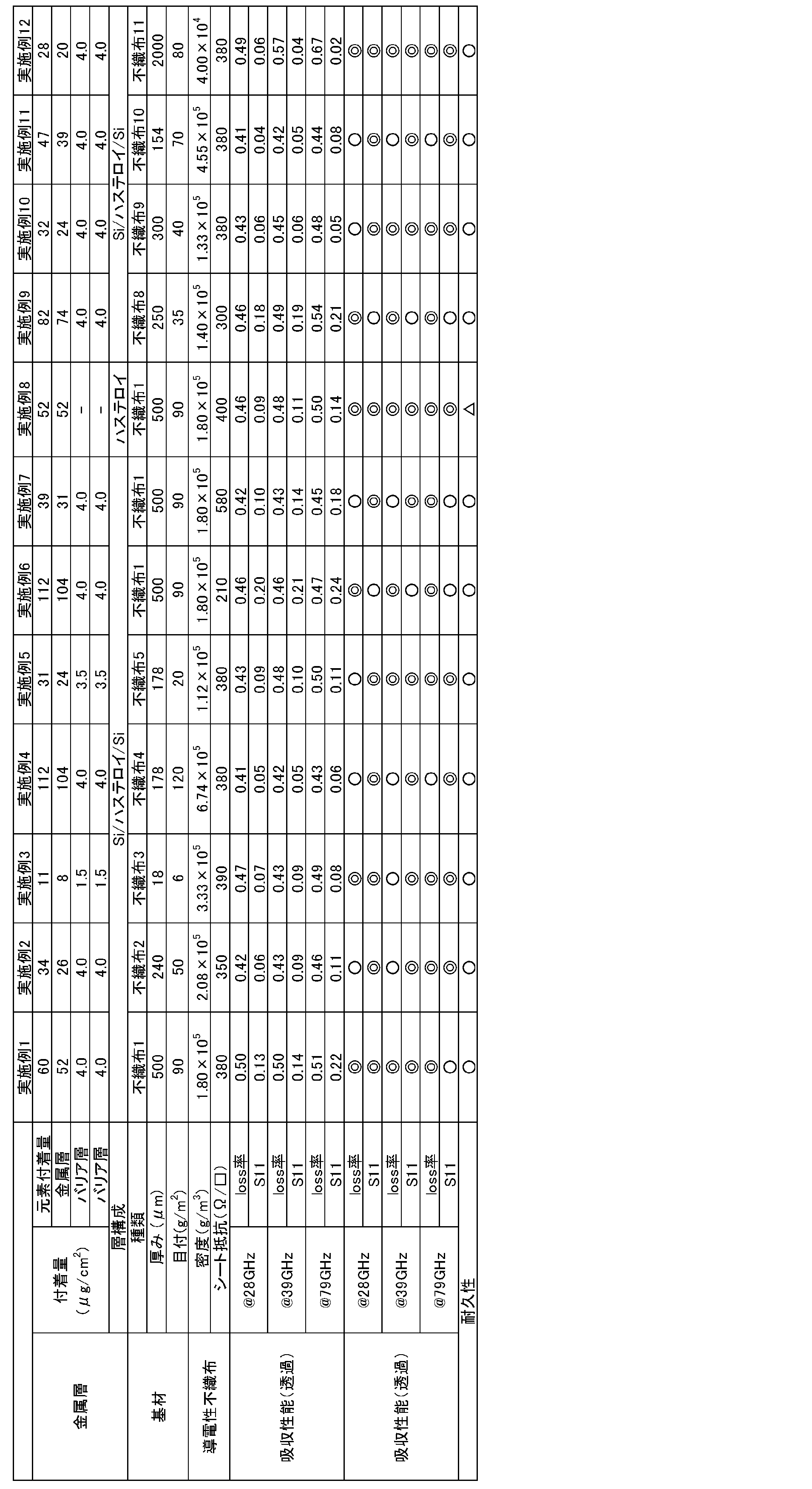
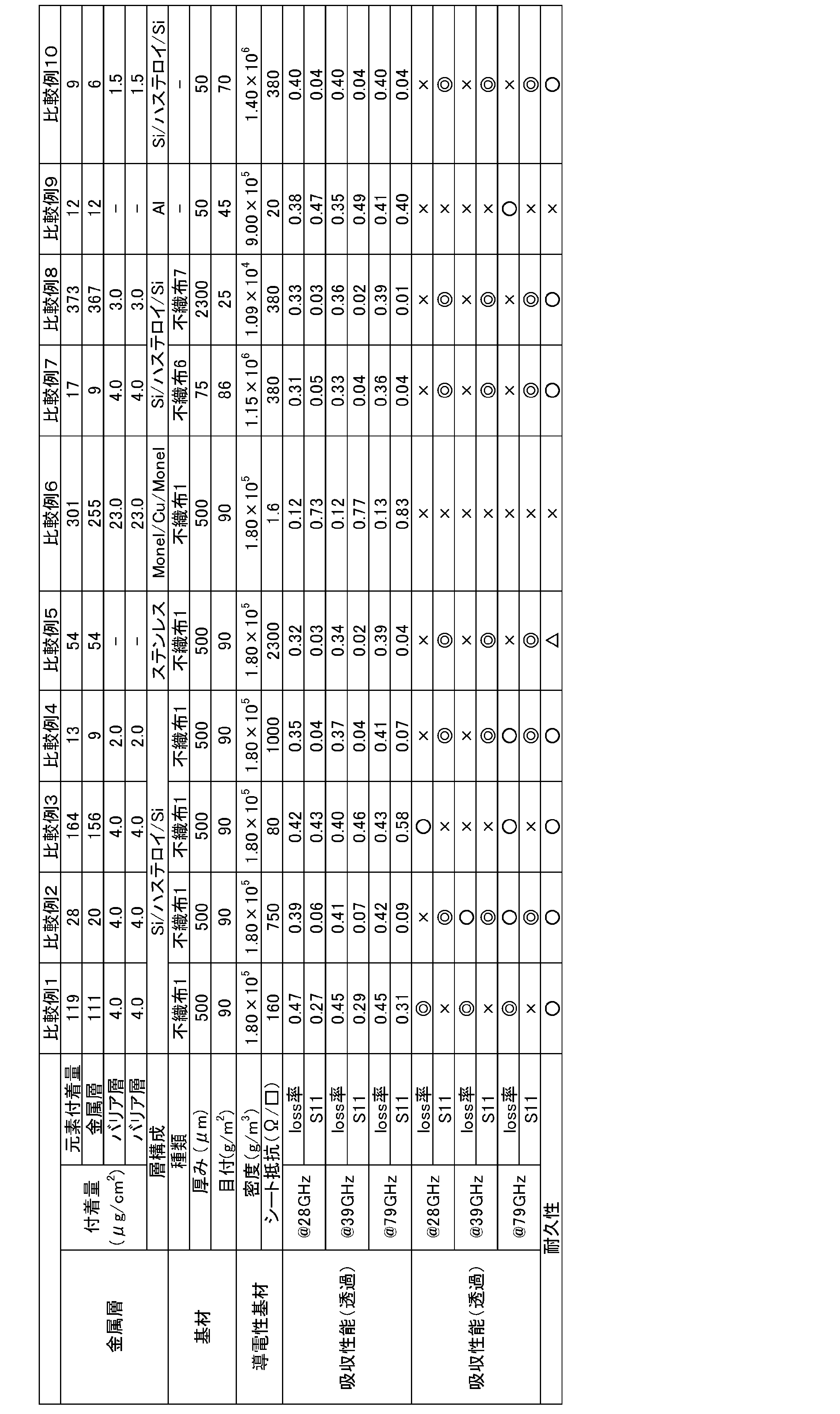
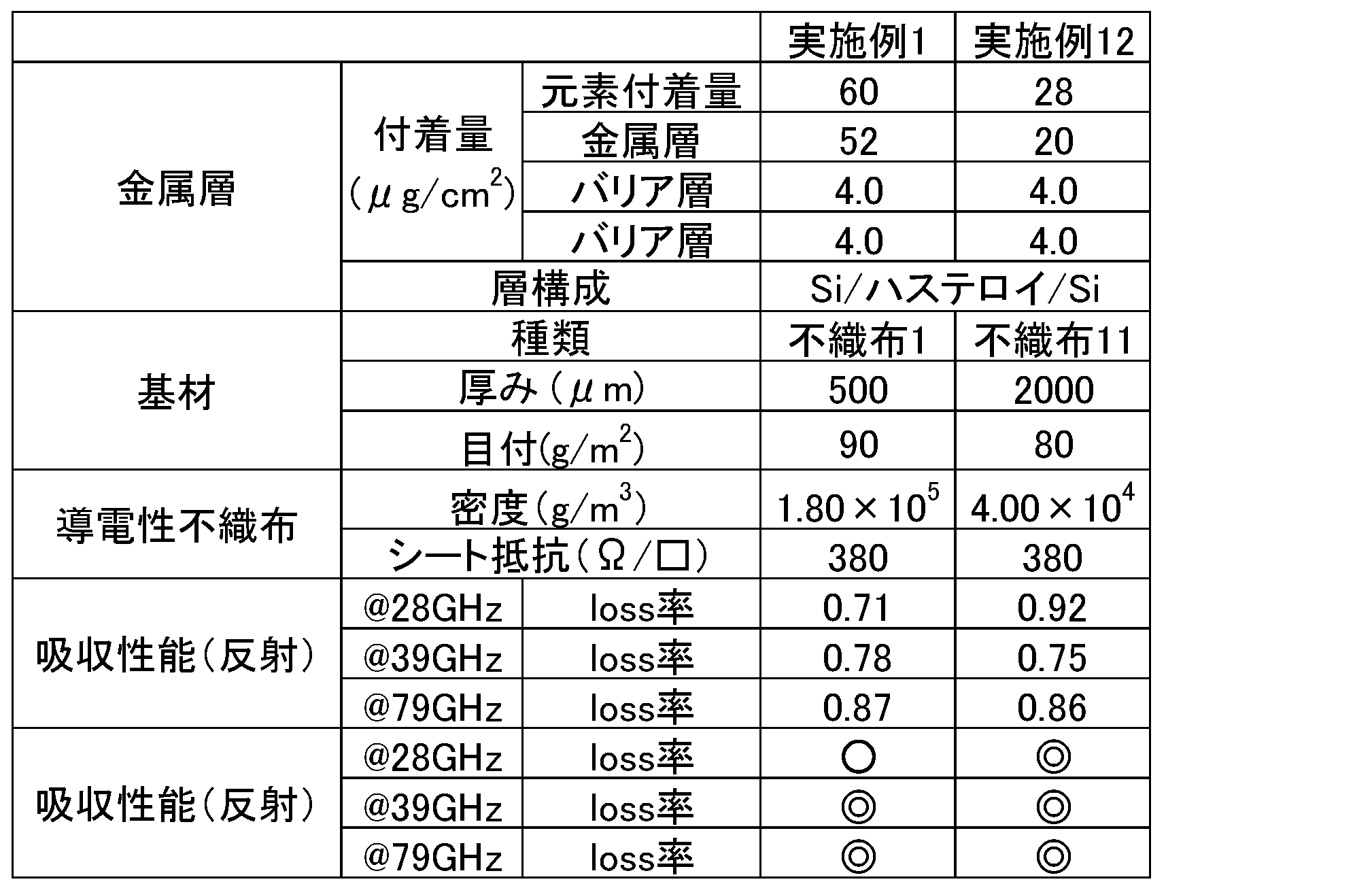
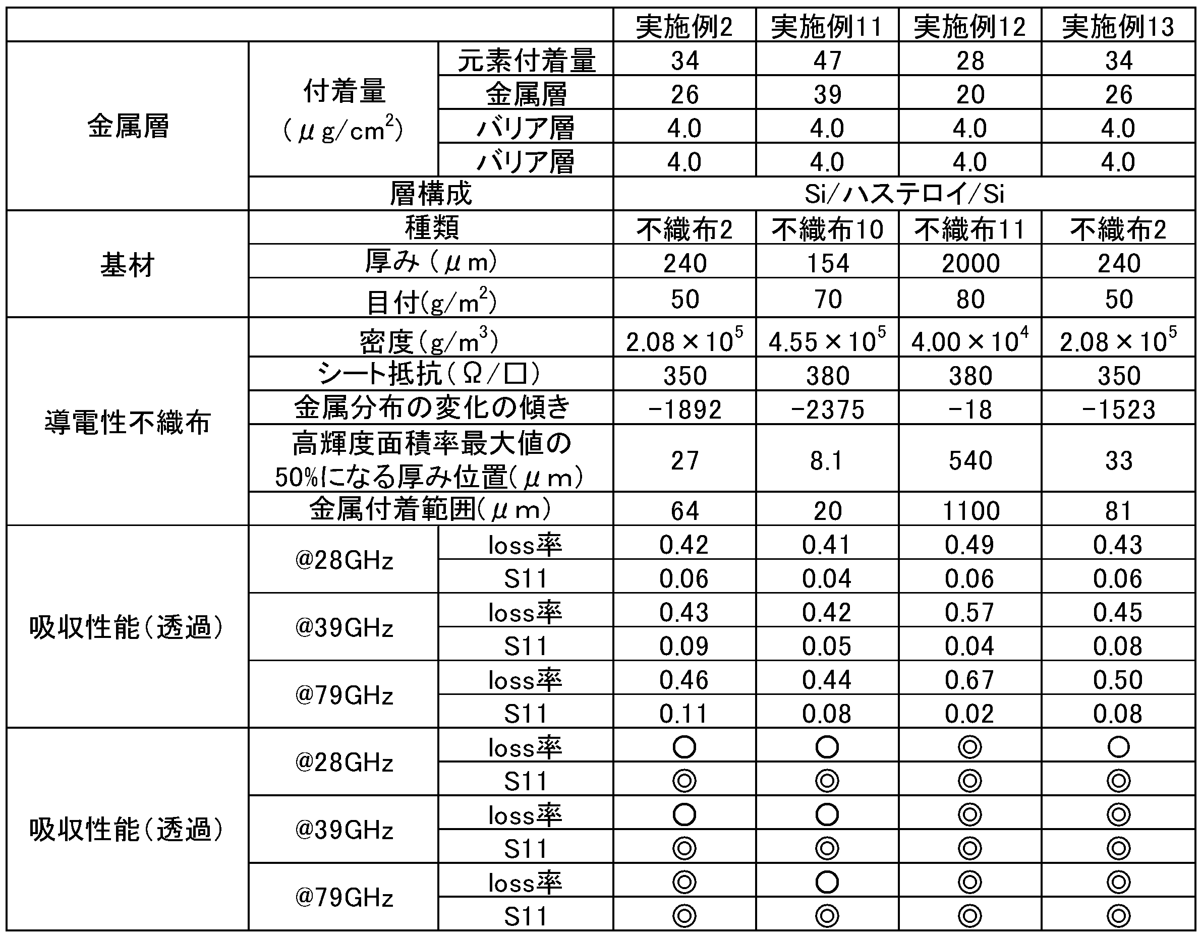
1 金属層
2 バリア層
3 不織布
4 金属筐体
5 導電性不織布(金属筐体内壁に配置)
6 導電性不織布(開口部に配置)
7 ICチップ
8 導電性不織布
9 樹脂筐体
10 導電性不織布(筐体内部に配置)
11 誘電体層
12 粘着剤層
13 反射層
2 バリア層
3 不織布
4 金属筐体
5 導電性不織布(金属筐体内壁に配置)
6 導電性不織布(開口部に配置)
7 ICチップ
8 導電性不織布
9 樹脂筐体
10 導電性不織布(筐体内部に配置)
11 誘電体層
12 粘着剤層
13 反射層
Claims (13)
- 少なくとも一方の面における金属層を有する導電性不織布であって、シート抵抗が200~600Ω/□であり、且つ密度が2.0×104~8.0×105g/m3である、導電性不織布。
- 金属元素及び/又は半金属元素付着量が5~150μg/cm2である、請求項1に記載の導電性不織布。
- 前記金属層の少なくとも一方の面上に、ニッケル、ケイ素、チタン、及びアルミニウムからなる群より選択される少なくとも1種の元素を含有するバリア層を有する、請求項1又は2に記載の導電性不織布。
- 前記金属層が、ニッケル、モリブデン、クロム、チタン、及びアルミニウムからなる群より選択される少なくとも1種の元素を含有する、請求項1~3のいずれかに記載の導電性不織布。
- X線CT装置により測定される高輝度面積率の変化の傾きが、-3000以上-10以下である、請求項1~4いずれかに記載の導電性不織布。
- 請求項1~5のいずれかに記載の導電性不織布を含む、電波吸収体。
- 前記導電性不織布が、更に接着剤層を備える、請求項6記載の電波吸収体。
- 前記導電性不織布の厚みdが、式(1):λ/16≦d(式中、λは対象とする電波の波長を示す。)を満たす、請求項6又は7に記載の電波吸収体。
- 前記導電性不織布と反射層を有し、前記導電性不織布のシート抵抗が200~600Ω/□である面とは他方の面に反射層を有する、請求項8記載の電波吸収体。
- 請求項6~9いずれか記載の電波吸収体を有する、筐体。
- 前記導電性不織布を前記筐体内面に有する、請求項10記載の筐体。
- 前記導電性不織布が、前記筐体の開口部に有する、請求項10記載の筐体。
- 請求項6~9いずれか記載の電波吸収体、又は、請求項10~12いずれか記載の筐体を有する、電子デバイス。
Priority Applications (3)
| Application Number | Priority Date | Filing Date | Title |
|---|---|---|---|
| US17/297,183 US20220007553A1 (en) | 2018-11-30 | 2019-11-28 | Conductive nonwoven fabric |
| JP2020514629A JP6846573B2 (ja) | 2018-11-30 | 2019-11-28 | 導電性不織布 |
| CN201980078298.9A CN113165339A (zh) | 2018-11-30 | 2019-11-28 | 导电性非织造布 |
Applications Claiming Priority (2)
| Application Number | Priority Date | Filing Date | Title |
|---|---|---|---|
| JP2018-224969 | 2018-11-30 | ||
| JP2018224969 | 2018-11-30 |
Publications (1)
| Publication Number | Publication Date |
|---|---|
| WO2020111210A1 true WO2020111210A1 (ja) | 2020-06-04 |
Family
ID=70853854
Family Applications (1)
| Application Number | Title | Priority Date | Filing Date |
|---|---|---|---|
| PCT/JP2019/046684 Ceased WO2020111210A1 (ja) | 2018-11-30 | 2019-11-28 | 導電性不織布 |
Country Status (5)
| Country | Link |
|---|---|
| US (1) | US20220007553A1 (ja) |
| JP (2) | JP6846573B2 (ja) |
| CN (1) | CN113165339A (ja) |
| TW (1) | TW202039245A (ja) |
| WO (1) | WO2020111210A1 (ja) |
Cited By (4)
| Publication number | Priority date | Publication date | Assignee | Title |
|---|---|---|---|---|
| WO2022039132A1 (ja) * | 2020-08-17 | 2022-02-24 | 積水化学工業株式会社 | 電波吸収シート |
| WO2022107538A1 (ja) * | 2020-11-19 | 2022-05-27 | 星和電機株式会社 | 電磁波吸収シート |
| WO2024029575A1 (ja) * | 2022-08-02 | 2024-02-08 | 積水化学工業株式会社 | 電波反射体、電波反射体の製造方法および電波反射体の施工方法 |
| WO2025047026A1 (ja) * | 2023-08-30 | 2025-03-06 | 国立大学法人東北大学 | 電磁波吸収体及び電磁波吸収方法 |
Families Citing this family (4)
| Publication number | Priority date | Publication date | Assignee | Title |
|---|---|---|---|---|
| US11925009B2 (en) * | 2021-03-09 | 2024-03-05 | Hamilton Sundstrand Corporation | Adaptive design and fabrication of radiation shielding inserts for electronic components |
| US12016164B1 (en) * | 2023-05-08 | 2024-06-18 | The Boeing Company | RF filter device for aircraft nacelle access door gap |
| JP7753307B2 (ja) * | 2023-09-15 | 2025-10-14 | 矢崎総業株式会社 | シールド電線 |
| DE112024000504T5 (de) | 2024-02-26 | 2026-03-12 | Yazaki Corporation | Abgeschirmtes elektrisches Kabel und leitfähiges Vliesband |
Citations (4)
| Publication number | Priority date | Publication date | Assignee | Title |
|---|---|---|---|---|
| JPH06104093A (ja) * | 1991-05-24 | 1994-04-15 | Japan Vilene Co Ltd | 導電性粘着シート |
| JP2008223189A (ja) * | 2007-03-15 | 2008-09-25 | Kuraray Co Ltd | 耐熱性に優れる導電性不織布 |
| JP2010106391A (ja) * | 2008-10-29 | 2010-05-13 | Daiwabo Holdings Co Ltd | 金属めっき繊維構造物及びそれを焼成してなる金属構造物 |
| JP2011146696A (ja) * | 2009-12-15 | 2011-07-28 | Asahi Kasei Fibers Corp | ノイズ吸収布帛 |
Family Cites Families (13)
| Publication number | Priority date | Publication date | Assignee | Title |
|---|---|---|---|---|
| US5761053A (en) * | 1996-05-08 | 1998-06-02 | W. L. Gore & Associates, Inc. | Faraday cage |
| US7105234B2 (en) * | 2001-03-30 | 2006-09-12 | Schlegel Systems, Inc. | Flame retardant corrosive resistant conductive fabric article and method |
| TW593833B (en) * | 2003-08-18 | 2004-06-21 | Helix Technology Inc | Method for plating a film to a non-ionized radiation fibrous fabric |
| JP4176723B2 (ja) * | 2004-02-10 | 2008-11-05 | 日本ジッパーチュービング株式会社 | 電磁波シールドガスケット及びその製造方法 |
| JP2007299906A (ja) * | 2006-04-28 | 2007-11-15 | Nitto Denko Corp | シート状電磁波シールド性構造体を具備する物品。 |
| JP2008205447A (ja) * | 2007-01-24 | 2008-09-04 | Toray Ind Inc | 電波吸収体 |
| WO2008093489A1 (ja) * | 2007-01-31 | 2008-08-07 | Kuraray Co., Ltd. | 電磁波吸収体 |
| US8324515B2 (en) * | 2007-10-16 | 2012-12-04 | Honeywell International Inc. | Housings for electronic components |
| JP2010157696A (ja) * | 2008-12-05 | 2010-07-15 | Toray Ind Inc | 電波吸収体 |
| JP5722775B2 (ja) * | 2009-07-24 | 2015-05-27 | 旭化成せんい株式会社 | 電磁波シールドシート |
| JP2012000947A (ja) * | 2010-06-21 | 2012-01-05 | Mitsui Mining & Smelting Co Ltd | セラミック系絶縁層と金属層との積層体及び当該積層体の製造方法 |
| JP2016157814A (ja) * | 2015-02-24 | 2016-09-01 | 王子ホールディングス株式会社 | 電波吸収体 |
| JP2017034000A (ja) * | 2015-07-29 | 2017-02-09 | ダイニック株式会社 | 電波吸収体用抵抗フィルム |
-
2019
- 2019-11-28 JP JP2020514629A patent/JP6846573B2/ja active Active
- 2019-11-28 WO PCT/JP2019/046684 patent/WO2020111210A1/ja not_active Ceased
- 2019-11-28 US US17/297,183 patent/US20220007553A1/en not_active Abandoned
- 2019-11-28 CN CN201980078298.9A patent/CN113165339A/zh active Pending
- 2019-11-29 TW TW108143762A patent/TW202039245A/zh unknown
-
2021
- 2021-02-19 JP JP2021025044A patent/JP2021103775A/ja active Pending
Patent Citations (4)
| Publication number | Priority date | Publication date | Assignee | Title |
|---|---|---|---|---|
| JPH06104093A (ja) * | 1991-05-24 | 1994-04-15 | Japan Vilene Co Ltd | 導電性粘着シート |
| JP2008223189A (ja) * | 2007-03-15 | 2008-09-25 | Kuraray Co Ltd | 耐熱性に優れる導電性不織布 |
| JP2010106391A (ja) * | 2008-10-29 | 2010-05-13 | Daiwabo Holdings Co Ltd | 金属めっき繊維構造物及びそれを焼成してなる金属構造物 |
| JP2011146696A (ja) * | 2009-12-15 | 2011-07-28 | Asahi Kasei Fibers Corp | ノイズ吸収布帛 |
Cited By (8)
| Publication number | Priority date | Publication date | Assignee | Title |
|---|---|---|---|---|
| WO2022039132A1 (ja) * | 2020-08-17 | 2022-02-24 | 積水化学工業株式会社 | 電波吸収シート |
| JPWO2022039132A1 (ja) * | 2020-08-17 | 2022-02-24 | ||
| JP7755485B2 (ja) | 2020-08-17 | 2025-10-16 | 積水化学工業株式会社 | 電波吸収シート |
| WO2022107538A1 (ja) * | 2020-11-19 | 2022-05-27 | 星和電機株式会社 | 電磁波吸収シート |
| JP2022080991A (ja) * | 2020-11-19 | 2022-05-31 | 星和電機株式会社 | 電磁波吸収シート |
| JP7575918B2 (ja) | 2020-11-19 | 2024-10-30 | 星和電機株式会社 | 電磁波吸収シート |
| WO2024029575A1 (ja) * | 2022-08-02 | 2024-02-08 | 積水化学工業株式会社 | 電波反射体、電波反射体の製造方法および電波反射体の施工方法 |
| WO2025047026A1 (ja) * | 2023-08-30 | 2025-03-06 | 国立大学法人東北大学 | 電磁波吸収体及び電磁波吸収方法 |
Also Published As
| Publication number | Publication date |
|---|---|
| US20220007553A1 (en) | 2022-01-06 |
| JPWO2020111210A1 (ja) | 2021-02-15 |
| CN113165339A (zh) | 2021-07-23 |
| TW202039245A (zh) | 2020-11-01 |
| JP2021103775A (ja) | 2021-07-15 |
| JP6846573B2 (ja) | 2021-03-24 |
Similar Documents
| Publication | Publication Date | Title |
|---|---|---|
| JP6846573B2 (ja) | 導電性不織布 | |
| US20130334472A1 (en) | Graphene based structures and methods for shielding electromagnetic radiation | |
| US11355453B2 (en) | Electronic assembly, electronic apparatus including the same and method for fabricating electronic assembly | |
| KR20040089097A (ko) | 로시 매체를 포함하는 emi실딩 | |
| JPWO2015076387A1 (ja) | ノイズ吸収シート | |
| WO2005081609A1 (ja) | 電磁波ノイズ抑制体、電磁波ノイズ抑制機能付構造体、およびそれらの製造方法 | |
| JP3874806B2 (ja) | 新規な導電性ループパターン及びこれを有する周波数選択性電磁波シールド材 | |
| KR102127363B1 (ko) | 투명 스텔스 구조체 | |
| US20170027089A1 (en) | Multi-functional sheet for shielding electromagnetic waves and dissipating heat at high performance | |
| JPWO2020067052A1 (ja) | 電波透過体 | |
| CN209328567U (zh) | 线材结构 | |
| WO2021221119A1 (ja) | 配線基板及び配線基板の製造方法 | |
| Tong | EMI shielding materials and absorbers for 5G communications | |
| KR20200004258A (ko) | 전자파 흡수 복합 시트 | |
| EP4460161A1 (en) | Sheet | |
| JP2022130302A (ja) | 電波吸収体用部材 | |
| JP2022130303A (ja) | 導電性繊維シート | |
| JP7564106B2 (ja) | 電波吸収体 | |
| JP2020013848A (ja) | 電磁波吸収接着シート | |
| KR20130014702A (ko) | 휴대용 전자기기에서의 전자파 차폐구 및 그 차폐방법 | |
| JP2020013847A (ja) | 電磁波吸収シート及び半導体装置 | |
| JP2022132148A (ja) | 難燃性ノイズ抑制繊維シート | |
| JP2020025093A (ja) | 電波吸収シート | |
| JP7305392B2 (ja) | λ/4型電波吸収体 | |
| JP7755485B2 (ja) | 電波吸収シート |
Legal Events
| Date | Code | Title | Description |
|---|---|---|---|
| ENP | Entry into the national phase |
Ref document number: 2020514629 Country of ref document: JP Kind code of ref document: A |
|
| 121 | Ep: the epo has been informed by wipo that ep was designated in this application |
Ref document number: 19889591 Country of ref document: EP Kind code of ref document: A1 |
|
| NENP | Non-entry into the national phase |
Ref country code: DE |
|
| 122 | Ep: pct application non-entry in european phase |
Ref document number: 19889591 Country of ref document: EP Kind code of ref document: A1 |