WO2020105298A1 - シリコンウェーハのヘリカル面取り加工方法 - Google Patents
シリコンウェーハのヘリカル面取り加工方法Info
- Publication number
- WO2020105298A1 WO2020105298A1 PCT/JP2019/039403 JP2019039403W WO2020105298A1 WO 2020105298 A1 WO2020105298 A1 WO 2020105298A1 JP 2019039403 W JP2019039403 W JP 2019039403W WO 2020105298 A1 WO2020105298 A1 WO 2020105298A1
- Authority
- WO
- WIPO (PCT)
- Prior art keywords
- chamfering
- wafer
- inclination angle
- silicon wafer
- angle
- Prior art date
- Legal status (The legal status is an assumption and is not a legal conclusion. Google has not performed a legal analysis and makes no representation as to the accuracy of the status listed.)
- Ceased
Links
Images




Classifications
-
- H—ELECTRICITY
- H10—SEMICONDUCTOR DEVICES; ELECTRIC SOLID-STATE DEVICES NOT OTHERWISE PROVIDED FOR
- H10P—GENERIC PROCESSES OR APPARATUS FOR THE MANUFACTURE OR TREATMENT OF DEVICES COVERED BY CLASS H10
- H10P52/00—Grinding, lapping or polishing of wafers, substrates or parts of devices
-
- H—ELECTRICITY
- H10—SEMICONDUCTOR DEVICES; ELECTRIC SOLID-STATE DEVICES NOT OTHERWISE PROVIDED FOR
- H10P—GENERIC PROCESSES OR APPARATUS FOR THE MANUFACTURE OR TREATMENT OF DEVICES COVERED BY CLASS H10
- H10P90/00—Preparation of wafers not covered by a single main group of this subclass, e.g. wafer reinforcement
- H10P90/12—Preparing bulk and homogeneous wafers
- H10P90/128—Preparing bulk and homogeneous wafers by edge treatment, e.g. chamfering
-
- B—PERFORMING OPERATIONS; TRANSPORTING
- B24—GRINDING; POLISHING
- B24B—MACHINES, DEVICES, OR PROCESSES FOR GRINDING OR POLISHING; DRESSING OR CONDITIONING OF ABRADING SURFACES; FEEDING OF GRINDING, POLISHING, OR LAPPING AGENTS
- B24B47/00—Drives or gearings; Equipment therefor
- B24B47/25—Drives or gearings; Equipment therefor for compensating grinding wheel abrasion resulting from dressing
-
- B—PERFORMING OPERATIONS; TRANSPORTING
- B24—GRINDING; POLISHING
- B24B—MACHINES, DEVICES, OR PROCESSES FOR GRINDING OR POLISHING; DRESSING OR CONDITIONING OF ABRADING SURFACES; FEEDING OF GRINDING, POLISHING, OR LAPPING AGENTS
- B24B49/00—Measuring or gauging equipment for controlling the feed movement of the grinding tool or work; Arrangements of indicating or measuring equipment, e.g. for indicating the start of the grinding operation
- B24B49/02—Measuring or gauging equipment for controlling the feed movement of the grinding tool or work; Arrangements of indicating or measuring equipment, e.g. for indicating the start of the grinding operation according to the instantaneous size and required size of the workpiece acted upon, the measuring or gauging being continuous or intermittent
-
- B—PERFORMING OPERATIONS; TRANSPORTING
- B24—GRINDING; POLISHING
- B24B—MACHINES, DEVICES, OR PROCESSES FOR GRINDING OR POLISHING; DRESSING OR CONDITIONING OF ABRADING SURFACES; FEEDING OF GRINDING, POLISHING, OR LAPPING AGENTS
- B24B49/00—Measuring or gauging equipment for controlling the feed movement of the grinding tool or work; Arrangements of indicating or measuring equipment, e.g. for indicating the start of the grinding operation
- B24B49/02—Measuring or gauging equipment for controlling the feed movement of the grinding tool or work; Arrangements of indicating or measuring equipment, e.g. for indicating the start of the grinding operation according to the instantaneous size and required size of the workpiece acted upon, the measuring or gauging being continuous or intermittent
- B24B49/04—Measuring or gauging equipment for controlling the feed movement of the grinding tool or work; Arrangements of indicating or measuring equipment, e.g. for indicating the start of the grinding operation according to the instantaneous size and required size of the workpiece acted upon, the measuring or gauging being continuous or intermittent involving measurement of the workpiece at the place of grinding during grinding operation
- B24B49/05—Measuring or gauging equipment for controlling the feed movement of the grinding tool or work; Arrangements of indicating or measuring equipment, e.g. for indicating the start of the grinding operation according to the instantaneous size and required size of the workpiece acted upon, the measuring or gauging being continuous or intermittent involving measurement of the workpiece at the place of grinding during grinding operation including the measurement of a first workpiece already machined and of another workpiece being machined and to be matched with the first one
-
- B—PERFORMING OPERATIONS; TRANSPORTING
- B24—GRINDING; POLISHING
- B24B—MACHINES, DEVICES, OR PROCESSES FOR GRINDING OR POLISHING; DRESSING OR CONDITIONING OF ABRADING SURFACES; FEEDING OF GRINDING, POLISHING, OR LAPPING AGENTS
- B24B49/00—Measuring or gauging equipment for controlling the feed movement of the grinding tool or work; Arrangements of indicating or measuring equipment, e.g. for indicating the start of the grinding operation
- B24B49/18—Measuring or gauging equipment for controlling the feed movement of the grinding tool or work; Arrangements of indicating or measuring equipment, e.g. for indicating the start of the grinding operation taking regard of the presence of dressing tools
- B24B49/183—Wear compensation without the presence of dressing tools
-
- B—PERFORMING OPERATIONS; TRANSPORTING
- B24—GRINDING; POLISHING
- B24B—MACHINES, DEVICES, OR PROCESSES FOR GRINDING OR POLISHING; DRESSING OR CONDITIONING OF ABRADING SURFACES; FEEDING OF GRINDING, POLISHING, OR LAPPING AGENTS
- B24B53/00—Devices or means for dressing or conditioning abrasive surfaces
- B24B53/06—Devices or means for dressing or conditioning abrasive surfaces of profiled abrasive wheels
-
- B—PERFORMING OPERATIONS; TRANSPORTING
- B24—GRINDING; POLISHING
- B24B—MACHINES, DEVICES, OR PROCESSES FOR GRINDING OR POLISHING; DRESSING OR CONDITIONING OF ABRADING SURFACES; FEEDING OF GRINDING, POLISHING, OR LAPPING AGENTS
- B24B53/00—Devices or means for dressing or conditioning abrasive surfaces
- B24B53/06—Devices or means for dressing or conditioning abrasive surfaces of profiled abrasive wheels
- B24B53/062—Devices or means for dressing or conditioning abrasive surfaces of profiled abrasive wheels using rotary dressing tools
-
- B—PERFORMING OPERATIONS; TRANSPORTING
- B24—GRINDING; POLISHING
- B24B—MACHINES, DEVICES, OR PROCESSES FOR GRINDING OR POLISHING; DRESSING OR CONDITIONING OF ABRADING SURFACES; FEEDING OF GRINDING, POLISHING, OR LAPPING AGENTS
- B24B53/00—Devices or means for dressing or conditioning abrasive surfaces
- B24B53/06—Devices or means for dressing or conditioning abrasive surfaces of profiled abrasive wheels
- B24B53/07—Devices or means for dressing or conditioning abrasive surfaces of profiled abrasive wheels by means of forming tools having a shape complementary to that to be produced, e.g. blocks, profile rolls
-
- B—PERFORMING OPERATIONS; TRANSPORTING
- B24—GRINDING; POLISHING
- B24B—MACHINES, DEVICES, OR PROCESSES FOR GRINDING OR POLISHING; DRESSING OR CONDITIONING OF ABRADING SURFACES; FEEDING OF GRINDING, POLISHING, OR LAPPING AGENTS
- B24B9/00—Machines or devices designed for grinding edges or bevels on work or for removing burrs; Accessories therefor
- B24B9/02—Machines or devices designed for grinding edges or bevels on work or for removing burrs; Accessories therefor characterised by a special design with respect to properties of materials specific to articles to be ground
- B24B9/06—Machines or devices designed for grinding edges or bevels on work or for removing burrs; Accessories therefor characterised by a special design with respect to properties of materials specific to articles to be ground of non-metallic inorganic material, e.g. stone, ceramics, porcelain
- B24B9/065—Machines or devices designed for grinding edges or bevels on work or for removing burrs; Accessories therefor characterised by a special design with respect to properties of materials specific to articles to be ground of non-metallic inorganic material, e.g. stone, ceramics, porcelain of thin, brittle parts, e.g. semiconductors, wafers
-
- H—ELECTRICITY
- H10—SEMICONDUCTOR DEVICES; ELECTRIC SOLID-STATE DEVICES NOT OTHERWISE PROVIDED FOR
- H10P—GENERIC PROCESSES OR APPARATUS FOR THE MANUFACTURE OR TREATMENT OF DEVICES COVERED BY CLASS H10
- H10P72/00—Handling or holding of wafers, substrates or devices during manufacture or treatment thereof
- H10P72/70—Handling or holding of wafers, substrates or devices during manufacture or treatment thereof for supporting or gripping
- H10P72/76—Handling or holding of wafers, substrates or devices during manufacture or treatment thereof for supporting or gripping using mechanical means, e.g. clamps or pinches
- H10P72/7604—Handling or holding of wafers, substrates or devices during manufacture or treatment thereof for supporting or gripping using mechanical means, e.g. clamps or pinches the wafers being placed on a susceptor, stage or support
- H10P72/7618—Handling or holding of wafers, substrates or devices during manufacture or treatment thereof for supporting or gripping using mechanical means, e.g. clamps or pinches the wafers being placed on a susceptor, stage or support characterised by a movable susceptor, stage or support, others than those only rotating on their own vertical axis, e.g. susceptors on a rotating carrousel
-
- H—ELECTRICITY
- H10—SEMICONDUCTOR DEVICES; ELECTRIC SOLID-STATE DEVICES NOT OTHERWISE PROVIDED FOR
- H10P—GENERIC PROCESSES OR APPARATUS FOR THE MANUFACTURE OR TREATMENT OF DEVICES COVERED BY CLASS H10
- H10P72/00—Handling or holding of wafers, substrates or devices during manufacture or treatment thereof
- H10P72/04—Apparatus for manufacture or treatment
- H10P72/0428—Apparatus for mechanical treatment or grinding or cutting
Definitions
- the present invention relates to a helical chamfering method for a silicon wafer, and more particularly to a helical chamfering method for setting a target wafer tilt angle at a silicon wafer edge to a low angle.
- Silicon wafers are widely used as substrates for semiconductor devices.
- a silicon wafer is obtained by subjecting a wafer obtained by slicing a single crystal silicon ingot to lapping and mirror polishing. Further, in order to prevent chipping or the like when a silicon wafer is transported, it is common to chamfer the edge portion of the wafer.
- FIG. 1A is a perspective view schematically showing the positional relationship between the silicon wafer W and the chamfering wheel 10 during helical chamfering.
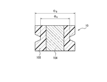
- FIG. 1B is a schematic cross-sectional view of the chamfering wheel 10 (illustrated as being horizontally installed for simplicity).
- the chamfering wheel 10 is provided with a precision grinding wheel portion 10B (also referred to as a resin grindstone or a resin bond grindstone) on the periphery of a central portion 10A made of metal.
- the chamfering wheel 10 is rotated while being inclined at a predetermined angle ⁇ (see FIG. 1A. The angle symbol ⁇ is not shown) with respect to the vertical direction.
- the silicon wafer W is pressed and brought into contact with the precision polishing grindstone portion 10B while being rotated, so that the edge portion of the silicon wafer W is subjected to a finish chamfering process (hereinafter, simply “chamfering process”).
- chamfering process Prior to this chamfering process, the shape of the fine grinding wheel portion 10B is preliminarily created by rough chamfering process using a rough grinding wheel.
- Truing is generally performed by the following procedure. First, a lure having a predetermined luer inclination angle is manufactured in consideration of the final wafer inclination angle of the edge portion of the silicon wafer W to be finally obtained within the allowable angle range of the target wafer inclination angle.
- the chamfering wheels 10 are pressed and brought into contact with each other while inclining the machining axis of the chamfering wheels 10 at a predetermined angle ⁇ with respect to the vertical direction, thereby machining the groove portions of the fine grinding wheel portion 10B of the chamfering wheels 10. In this way, the shape of the edge of the truer is transferred to the groove portion of the precision grinding wheel portion 10B.
- the shape of the chamfered portion of the silicon wafer W is affected by the groove shape of the fine grinding wheel portion 10B derived from the tilter inclination angle and the processing axis inclination (inclination angle ⁇ ) of the chamfering wheel.
- the finished shape of the edge portion of the silicon wafer is not simply transferred as it is to the groove shape of the fine grinding wheel portion 10B. Therefore, in order to obtain a desired finished shape, it is necessary to properly prepare the chamfered shape of the truer and appropriately adjust the groove shape of the fine grinding wheel portion 10B.
- Patent Document 1 discloses the following method for processing a chamfered portion of a semiconductor wafer. That is, in a method of processing a roughly ground chamfered portion of a semiconductor wafer by precisely tilting the wafer and a second grindstone relative to each other, a groove having a vertically asymmetrical shape is formed around the groove. No. 1 grindstone is used to grind the edge of the disk-shaped luer in the groove of the first grindstone, thereby forming the edge of the luer into a vertically asymmetrical groove shape of the first grindstone. A groove is formed around the second grindstone by grinding the second grindstone while inclining it relative to the second grindstone, and with respect to the groove direction formed around the second grindstone. The chamfered portion of the wafer is finely ground by inclining the semiconductor wafer relatively.
- the present inventor sets the chamfered shape of the truer inclination angle to a low inclination angle in order to set the finished wafer inclination angle of the silicon wafer edge to a lower angle (hereinafter, may be abbreviated as “low inclination angle”) than before.
- low inclination angle a lower angle
- the desired finished wafer inclination angle could not be achieved at the beginning of using the polishing wheel, but at the end of using the polishing wheel, the desired finishing wafer inclination angle could be achieved. There was a case. Further, when using a luer having a different luer inclination angle, although the desired finished wafer inclination angle could be realized in the initial stage of using the polishing wheel, the desired finished wafer inclination angle may not be gradually realized. .. As a result of further detailed analysis, when the desired finished wafer inclination angle could be realized, the groove bottom diameter ⁇ A (see FIG. 1B) of the chamfering wheel was within the predetermined range.
- the groove bottom diameter ⁇ A of the chamfer wheel hardly affected the finished wafer inclination angle. Therefore, if a conventional finished wafer inclination angle is obtained, one chamfering wheel can be used from the beginning to the end of use of the precision grinding wheel.
- the number of processings (wheel life) that can be processed by one grinding wheel is conventionally performed only by using a luer having a specific luer inclination angle. It will decrease sharply compared to technology. If the frequency of exchanging the grinding wheel increases, the production cost at the time of mass production will be greatly affected, and the present inventor has recognized this as a new problem.
- an object of the present invention is to provide a method for chamfering a silicon wafer, which can increase the number of times that a chamfering wheel used for helical chamfering can be processed when the finished wafer inclination angle is set to a low angle.
- the present inventor diligently studied to solve the above problems. Then, in order to keep the finished wafer tilt angle within the allowable angle range of the target wafer tilt angle, it is possible to increase the number of times the chamfering wheel can be processed by properly using the truer tilt angle according to the groove bottom diameter of the chamfering wheel. The inventor has found out.
- the present invention is based on the above findings, and its gist configuration is as follows.
- the edge of the one silicon wafer by pressingly contacting the one polishing wafer part while rotating one silicon wafer while rotating the chamfering wheel equipped with the polishing wheel part with an inclination with respect to the vertical direction.
- the chamfering method of the silicon wafer which is the chamfering processing of the helical so that the finished wafer inclination angle in the part satisfies the allowable angle range of the target wafer inclination angle, and the helical chamfering processing is sequentially performed on a plurality of silicon wafers, A first truing step of truing the fine grinding wheel portion of the chamfering wheel using a truar having a first truar inclination angle; A helical chamfering process is performed on the first silicon wafer by using the refined grindstone portion after the first truing step, and the finished wafer inclination angle of the processed first silicon wafer is set to the target wafer inclination angle.
- a first chamfering process for machining within an allowable angle range A step of obtaining a groove bottom diameter of the grindstone portion after passing through the first chamfering step, A second truing step of truing the fine grinding wheel portion of the chamfering wheel by using a truer having a second truer inclination angle when the groove bottom diameter is smaller than a predetermined threshold value; A second silicon wafer is helically chamfered by using the fine grinding wheel portion after passing through the second truing step, and the finished wafer inclination angle of the second silicon wafer after the processing is set to the target wafer inclination angle.
- a second chamfering process that processes within the allowable angle range Including, The method for helically chamfering a silicon wafer, wherein the second truer inclination angle is larger than the first truer inclination angle.
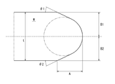
- FIG. 2A shows the thickness t of the peripheral portion of the wafer, the chamfering angle ⁇ 1 , the chamfering angle ⁇ 2 , and the chamfering width A, respectively.
- the dimensions B 1 and B 2 are the thickness of the upper surface and the thickness of the lower surface, respectively.
- BC is the length of the end face in the wafer thickness direction, and the length BC of the end face in the wafer thickness direction is zero in the chamfered shape shown in FIG. 2A.
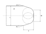
- FIG. 2B shows the shape of the peripheral portion of the wafer when the length BC in the wafer thickness direction is not zero.
- each of the upper surface chamfer angle ⁇ 1 and the lower surface chamfer angle ⁇ 2 corresponds to the wafer inclination angle ⁇ .
- the same definition will be applied even when a subscript is added to the wafer inclination angle ⁇ .
- the wafer inclination angles of the upper surface and the lower surface shall refer to the wafer inclination angles of both the upper surface and the lower surface.
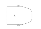
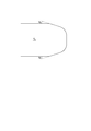
- the edge part of the truer 3 is composed of a chamfered slope (slope) 3A and a curved (usually parabolic) end 3B. Therefore, the angle formed by the chamfered slope 3A of the lure 3 and the main surface of the lure is defined as the lure inclination angle ⁇ .
- the same definition is applied when a suffix is attached to the luer inclination angle ⁇ . It should be noted that in the truer 3, abrasive grains are present on the curved end 3B, and processing is performed along the curved surface.
- the present invention it is possible to provide a method for chamfering a silicon wafer that can increase the number of times a chamfering wheel used for helical chamfering can be processed even when the finished wafer is inclined at a low angle.
- FIG. 1A It is a perspective view explaining the general helical chamfering processing method. It is a schematic cross section of the chamfering wheel in FIG. 1A. It is an example of a schematic cross-sectional view illustrating a wafer tilt angle ⁇ of a silicon wafer in the present specification. 5 is another example of a schematic cross-sectional view illustrating a wafer tilt angle ⁇ of a silicon wafer in the present specification. It is a schematic cross section explaining the luer inclination-angle (alpha) of the lure in this specification. 6 is a graph showing the relationship between the groove bottom diameter and the truer inclination angle of the fine grinding wheel and the finished wafer inclination angle of the silicon wafer according to the experiments of the present inventors.
- FIG. 6 is a flowchart of a method for chamfering a silicon wafer according to an embodiment of the present invention. It is a schematic cross section explaining a 1st truing process. It is a schematic cross section which shows the wafer inclination angle of the silicon wafer after the 1st chamfering process step. It is a schematic cross section explaining the truer 32 used for a 2nd truing process. It is a schematic cross section which shows the wafer inclination angle of the silicon wafer after the 2nd chamfering process step.
- the silicon wafer W A having a diameter of about 300 mm and the chamfering wheel 10 are respectively rotated while being pressed and brought into contact with each other in the groove portion of the polishing wheel portion 10B.
- Helical chamfering was applied to the edge of W A.
- the wafer tilt angle theta A silicon wafer W A after helical chamfering was measured using Kobelco Co. edge profile monitor (LEP-2200).
- the groove bottom diameter ⁇ A of the chamfering wheel 10 after the helical chamfering was measured by using W-GM-5200 manufactured by Tosei Engineering Co., Ltd.
- the target wafer inclination angle ⁇ 0 is set to a predetermined angle of 23 ° or less (for example, 20 ° or 18 °), the actual finished wafer inclination angle ⁇ after processing becomes smaller as the groove bottom diameter ⁇ A wears down. It is observed that the fluctuation gradually becomes saturated.
- the finished wafer tilt angle ⁇ is the allowable angle range of the target wafer tilt angle ⁇ 0. Deviate from. That is, if the luer tilt angle is fixed, the chamfering wheel cannot be used in the entire wheel life range, unlike the case where the target wafer tilt angle ⁇ 0 is more than 23 °.
- the desired finished wafer inclination angle ⁇ can be stably obtained. It is possible. For example, when the target wafer inclination angle ⁇ 0 is 18 ° and the allowable angle range is ⁇ 0.5 °, the groove bottom diameter ⁇ A is depleted to about 45.2 mm and then the truer inclination angle is 16 °. For example, the finished wafer inclination angle ⁇ after processing satisfies 18 ° ⁇ 0.5 °.
- the chamfering wheel since the chamfering wheel reaches the end of its life, it is necessary to replace the chamfering wheel as soon as possible. Therefore, in order to widely use the wheel life of the chamfering wheel, it is necessary to properly use the luer tilt angle according to the groove bottom diameter ⁇ A so that the finished wafer tilt angle ⁇ is within the allowable angle range of the target wafer tilt angle ⁇ 0.
- the inventor made an idea through the above experiment.
- the wheel life range will be specified. It can be used more effectively than when using only lures with an inclination angle.
- a threshold value is provided to the groove bottom diameter phi A of the chamfering wheel 10, the Mizosoko ⁇ phi A inventors that selectively using truer inclination angle according to is was conceived.
- FIGS. 5 to 9 show the main parts of the present invention, and a support base and a rotation mechanism for rotating each component are omitted for convenience of description.
- a chamfering method of a silicon wafer according to an embodiment of the present invention is such that a chamfering wheel 10 including a fine grinding wheel portion 10B is tilted and rotated with respect to a vertical direction and one silicon wafer is rotated while the fine grinding wheel portion 10B is being rotated.
- the helical chamfering process is performed so that the finished wafer inclination angle ⁇ at the edge portion of the one silicon wafer satisfies the allowable angle range of the target wafer inclination angle ⁇ 0 by pressing and contacting with each other. This is sequentially performed on silicon wafers.
- the "plurality of silicon wafers" referred to here are silicon wafers of the same type that are subjected to a series of chamfering processes according to the present processing method (e.g., in the same lot, where the wafer characteristics are substantially the processed shape after the helical chamfering process). Those that have no effect).
- a first silicon wafer W A and a second silicon wafer W B, which will be described later, are silicon wafers of the same kind in this sense.
- the target wafer inclination angle ⁇ 0 in this method is particularly preferably 23 ° or less.
- the groove bottom diameter ⁇ A is dependent on the chamfering process in which the target wafer inclination angle ⁇ 0 is 23 ° or less. Further, the target wafer tilt angle ⁇ 0 and its allowable angle range are appropriately determined according to the product specifications. Depending on the product specifications, the allowable angle range, which is the difference between the finished wafer tilt angle ⁇ and the target wafer tilt angle ⁇ 0 , can be appropriately set to ⁇ 0.1 ° to ⁇ 1.0 ° or the like.
- This method uses a first truer 31 having a first truer inclination angle ⁇ 1 to perform a first truing step S10 of truing the fine grinding wheel portion 10B of the chamfering wheel 10 and a first truing step S10.
- the first silicon wafer W A is subjected to a helical chamfering process using the polishing wheel part 10 B of the above, and the finished wafer inclination angle ⁇ A of the processed first silicon wafer W A is the allowable angle of the target wafer inclination angle ⁇ 0 .
- a first chamfering step S20 for processing within the range a step S30 for obtaining the groove bottom diameter ⁇ A of the fine grinding wheel portion 10B after passing through the first chamfering step S20, and a threshold value for which the groove bottom diameter ⁇ A is obtained in advance.
- the second truer 32 having the second truer inclination angle ⁇ 2 is used to perform the second truing step S40 of truing the fine grinding wheel portion 10B of the chamfering wheel 10 and the second truing step S40.
- the first truing step S10 will be described with reference to FIG.
- the first truer 31 having the first truer inclination angle ⁇ 1 is prepared (see step S11 in FIG. 6).
- the magnitude of the first truer tilt angle ⁇ 1 is arbitrary as long as the finished wafer tilt angle ⁇ A can be processed within the allowable angle range of the target tilt angle ⁇ 0 in the next second step. It may be appropriately selected according to the target wafer inclination angle ⁇ 0 and the groove bottom diameter ⁇ A. Generally, the magnitude of the first truer tilt angle ⁇ 1 is smaller than the target wafer tilt angle ⁇ 0 by 2.0 ° or more.
- the precision grinding wheel portion 10B is trued.
- a shape derived from the edge shape of the first truer 31 is formed on the precision grinding wheel portion 10B after the shape transfer. Referring to steps S12 and S13 in FIG. 6, the broken line portion in S13 corresponds to the groove of the fine grinding wheel portion 10B before truing in S12.
- the chamfering wheel 10 a general wheel used for helical chamfering can be used.
- the rotary shaft portion 10A is usually made of a metal such as aluminum or stainless steel, and a precision grinding wheel portion 10B is provided on the peripheral portion thereof, which is usually made of synthetic resin (the fine grinding stone portion 10B is a resin grinding stone. Or also referred to as a resin bond grindstone.).
- the fine grinding stone portion 10B is a resin grinding stone. Or also referred to as a resin bond grindstone.
- a hollow portion for the rotating shaft is provided in the rotating shaft portion 10A of the chamfering wheel, it is not shown for simplification of the drawing.
- a first chamfering step S20 subsequent to the first truing step S10 the silicon wafer W A is helically chamfered by the fine grinding wheel portion 10B transferred via the first truer 31 in the first truing step S10. ..
- the first silicon wafer W A is pressed and brought into contact with the fine grinding wheel portion 10B by pressing and rotating contact. Helical chamfering.
- the helical chamfering process is performed so that the finished wafer tilt angle ⁇ A of the processed first silicon wafer W A falls within the allowable angle range of the target wafer tilt angle ⁇ 0 .
- FIG. 7 illustrates the finished wafer tilt angle ⁇ A of the first silicon wafer W A thus formed.
- the wheel inclination angle ⁇ of the chamfering wheel 10 is appropriately set within the range of 4 ° to 15 °. Normally, the wheel tilt angle during truing and the wheel tilt angle during chamfering are matched.
- the groove bottom diameter ⁇ A may be measured after performing the helical chamfering process in the first chamfering process multiple times (100 units or 1000 units, etc.), or every time the helical machining is performed, the groove bottom diameter is measured.
- ⁇ A may be measured, or the groove bottom diameter ⁇ A may be measured at an appropriate timing. Further, it is also possible to previously obtain the amount of wear due to processing a plurality of times and measure the groove bottom diameter ⁇ A after the predetermined number of times has been exceeded.
- the groove bottom diameter ⁇ A can be measured by using a wheel groove diameter measuring device or a caliper mounted on a chamfering device (for example, W-GM-5200 manufactured by Tosei Engineering Co., Ltd.).
- the second truing step S40 is performed under the condition different from the first truing step S10. As shown in FIG. 8, a second truer 32 having a second truer inclination angle ⁇ 2 is prepared, and in the second truing step S40, this is used to true the fine grinding wheel portion 10B of the chamfering wheel 10. If the threshold value ⁇ 0 is determined by experimentally obtaining the correspondence between the groove bottom diameter ⁇ A and the first truer inclination angle ⁇ 1 and the finished wafer inclination angle ⁇ actually formed by processing. Good.
- the truing condition of the second truing process is different from that of the first truing process.
- Other truing conditions are preferably the same in the first truing step and the second truing step, but may be appropriately changed within a range that does not significantly affect the finished wafer inclination angle.
- the first luer inclination angle ⁇ 1 and the second luer inclination angle ⁇ 2 Is preferably 1 ° or more, and more preferably 2 ° or more.
- the upper limit is not limited, but may be 6 ° or less, for example.
- the second silicon wafer W B is subjected to a helical chamfering process in the same manner as in the first chamfering process step S20 by using the fine-polishing grindstone portion 10B that has passed through the second truing process S40.
- the helical chamfering process is performed so that the finished wafer tilt angle ⁇ B of the processed second silicon wafer W B is within the allowable angle range of the target wafer tilt angle ⁇ 0 .
- FIG. 9 illustrates the finished wafer inclination angle ⁇ B of the second silicon wafer W B.
- both theta B target wafer tilt angle theta It can be within an allowable angle range of 0 .
- the truer tilt angle is properly used according to the groove bottom diameter ⁇ A of the chamfering wheel 10.
- it can be controlled within the allowable angle range of both the finished wafer tilt angle theta B target wafer tilt angle theta 0 of the first silicon wafer W A finished wafer tilt angle theta A and the second silicon wafer W B of
- the number of times the chamfering wheel used for helical chamfering can be processed can be increased.
- the groove bottom diameter ⁇ A and the luer tilt angle it may be difficult to set the finished wafer tilt angle within the allowable range of the target wafer tilt angle. Therefore, in such a case, it is also preferable to further perform an adjusting step of adjusting the groove bottom diameter ⁇ A by depleting the precision grinding wheel portion 10B.
- the term "wear reduction” includes not only wear due to truing but also chamfering of a silicon wafer having a different target wafer tilt angle. This will not waste the life of the chamfer wheel.
- a third truer (further, a fourth truer) is used to perform a third truing step and a third chamfering step. May be further performed.
- a third truer further, a fourth truer
- ⁇ A wears out, it is possible to fully utilize the wheel life range by using a luer with a large luer inclination angle.
- the plane orientation of the silicon wafer is arbitrary, and a (100) plane wafer or a (110) plane wafer may be used.
- the silicon wafer may be doped with a dopant such as boron (B), phosphorus (P), arsenic (As), antimony (Sb), or carbon (C) or nitrogen (N) to obtain desired characteristics. May be doped. Further, the oxygen concentration of the silicon wafer is also arbitrary.
- a dopant such as boron (B), phosphorus (P), arsenic (As), antimony (Sb), or carbon (C) or nitrogen (N) to obtain desired characteristics. May be doped. Further, the oxygen concentration of the silicon wafer is also arbitrary.
- the diameter of the silicon wafer to be processed is not limited at all.
- the present invention can be applied to a typical silicon wafer having a diameter of 300 mm or 200 mm.
- the present invention can be applied to a silicon wafer having a diameter larger than 300 mm and a silicon wafer having a small diameter.
- the "silicon wafer” in this specification refers to a so-called “bulk” silicon wafer in which another layer such as an epitaxial layer or an insulating film made of silicon oxide is not formed on the surface. However, a natural oxide film having a film thickness of about several ⁇ may be formed. Further, with respect to the silicon wafer obtained by the present invention, another layer such as an epitaxial layer may be separately formed to prepare an epitaxial silicon wafer, and it may be used as a supporting substrate or a substrate for an active layer of a bonded wafer. An SOI (Silicon on Insulator) wafer may be manufactured. The "bulk" silicon wafer that serves as the base substrate for such wafers is the silicon wafer herein.
- the present invention it is possible to provide a method for chamfering a silicon wafer that can increase the number of times that a chamfering wheel used for helical chamfering can be processed when the finished wafer inclination angle is set to a low angle.
Landscapes
- Engineering & Computer Science (AREA)
- Mechanical Engineering (AREA)
- Chemical & Material Sciences (AREA)
- Ceramic Engineering (AREA)
- Inorganic Chemistry (AREA)
- Mechanical Treatment Of Semiconductor (AREA)
- Grinding-Machine Dressing And Accessory Apparatuses (AREA)
- Grinding And Polishing Of Tertiary Curved Surfaces And Surfaces With Complex Shapes (AREA)
Abstract
仕上がりウェーハ傾斜角度を低角度とする場合に、ヘリカル面取り加工に用いる面取りホイールの加工可能回数を増大できるシリコンウェーハの面取り加工方法を提供する。シリコンウェーハWのエッジ部における仕上がりウェーハ傾斜角度θが目標ウェーハ傾斜角度θ0の許容角度範囲内を満足するようヘリカル面取り加工するシリコンウェーハの面取り加工方法において、第1ツルーイング工程S10と、第1面取り加工工程S20と、前記第1面取り加工工程を経た後の前記砥石部10の溝底径φAを求める工程S30と、第2ツルーイング工程S40と、第2面取り工程S50と、を含み、前記第2のツルアー傾斜角度α2を、前記第1のツルアー傾斜角度α1よりも小さくする。
Description
本発明は、シリコンウェーハのヘリカル面取り加工方法に関し、特に、シリコンウェーハエッジ部の目標ウェーハ傾斜角度を低角度とする場合のヘリカル面取り加工方法に関する。
半導体デバイスの基板として、シリコンウェーハが広く用いられている。シリコンウェーハは、単結晶シリコンインゴットをスライスして得られるウェーハに対してラッピング加工及び鏡面研磨加工を施すことにより得られる。また、シリコンウェーハを搬送するときのチッピングなどを防止するため、ウェーハエッジ部に面取り加工を施すことが一般的である。
こうした面取り加工方法として、ウェーハエッジ部の面取り部の加工歪みを低減させるために、シリコンウェーハに対して面取りホイールを傾斜させて面取り加工を行う「ヘリカル面取り加工法」が知られている。図1A、図1Bを参照して、一般的なヘリカル面取り加工法を説明する。図1Aはヘリカル面取り加工時のシリコンウェーハWと面取りホイール10との位置関係を模式的に示す斜視図である。図1Bは面取りホイール10の模式断面図(簡便のため水平設置したときの様子を図示した)である。図1Bに、面取りホイール10の溝底径φA及びホイール径φBをそれぞれ図示する。面取りホイール10は金属製の中心部10Aの周縁に、精研砥石部10B(レジン砥石又はレジンボンド砥石とも呼ばれる)が設けられている。面取りホイール10を垂直方向に対して所定角度ψ(図1Aを参照。角度記号ψは図示せず。)で傾斜させながら、面取りホイール10を回転させる。そして、シリコンウェーハWを回転させながら精研砥石部10Bと押圧接触させることにより、シリコンウェーハWのエッジ部が仕上げ面取り加工(以下、単に「面取り加工」)される。なお、この面取加工に先立ち、粗研砥石を使用した粗面取加工によって精研砥石部10Bの形状は予め作り込まれている。
面取り加工後のシリコンウェーハWのエッジ部の形状を所望の仕上がりウェーハ傾斜角度に制御するため、面取りホイール10における精研砥石部10Bの溝形状のツルーイングが行われる。ツルーイングは、一般的には以下の手順により行われる。まず、最終的に得るべきシリコンウェーハWのエッジ部の仕上がりウェーハ傾斜角度が目標ウェーハ傾斜角度の許容角度範囲内となるよう勘案して、所定のツルアー傾斜角度を備えるツルアーを作製する。そして、このツルアーを用いて、面取りホイール10の加工軸を垂直方向に対して所定角度ψで傾斜させながら両者を押圧回転接触させ、面取りホイール10の精研砥石部10Bの溝部分を加工する。こうして、ツルアー縁部の形状が精研砥石部10Bの溝部分に転写される。
このように、シリコンウェーハWの面取り部の形状はツルアー傾斜角度由来の精研砥石部10Bの溝形状及び面取りホイールの加工軸傾斜(傾斜角ψ)の影響を受ける。ヘリカル面取り加工法において、シリコンウェーハエッジ部の仕上がり形状は精研砥石部10Bの溝形状がそのまま単純転写されるわけではない。そのため、所望の仕上がり形状を得るためにはツルアーの面取り形状を適切に作製し、精研砥石部10Bの溝形状を適切に調整する必要がある。
例えば特許文献1には、以下の半導体ウェーハの面取り部の加工方法が開示されている。すなわち、半導体ウェーハの粗研削された面取り部を、該ウェーハと第2の砥石とを相対的に傾けて精研削することにより加工する方法において、上下非対称の形状の溝が周囲に形成された第1の砥石を用い、該第1の砥石の溝で円盤状のツルアーの縁部を研削することにより該ツルアーの縁部を前記第1の砥石の上下非対称の溝形状に成形し、該ツルアーと第2の砥石とを相対的に傾けて該第2の砥石を研削することにより該第2の砥石の周囲に溝を形成し、該第2の砥石の周囲に形成された溝方向に対して前記半導体ウェーハを相対的に傾けて該ウェーハの面取り部を精研削する。
特許文献1の加工方法は、ヘリカル面取り加工を行うとウェーハ面取り部の上下の対称性が崩れるため、これを防止するために上下非対称の溝形状の粗研砥石(第1の砥石)を採用し、これに由来する溝形状を精研砥石(第2の砥石)に形成する、というものである。
ところで近年、シリコンウェーハエッジ部の面取り形状には種々の仕様が求められている。シリコンウェーハのエッジ部における仕上がりウェーハ傾斜角度を従来よりも低角度(水平に近い傾斜)とする要請もある。本発明者は、こうした低角度の仕上がりウェーハ傾斜角度を実現可能であるか、まず鋭意検討した。
本発明者は、シリコンウェーハエッジ部の仕上がりウェーハ傾斜角度を従来よりも低角度(以下、「低傾斜角」と略称することがある。)とするため、ツルアー傾斜角度を低傾斜角に面取り形状としたツルアーを用いることをまず試みた。そして、量産を想定してこのツルアーを用いて面取りホイールの精研砥石部をツルーイングし、ツルーイング後の精研砥石部によりシリコンウェーハのヘリカル面取り加工を繰り返し行った。すると、所望の低角度の仕上がりウェーハ傾斜角度を実現できる場合とできない場合とがあることを本発明者は確認した。より詳細に検討した結果、あるツルアーを用いた場合、精研砥石使用開始初期では所望の仕上がりウェーハ傾斜角度を実現できなかったものの、精研砥石使用末期には所望の仕上がりウェーハ傾斜角度を実現できた場合があった。また、別のツルアー傾斜角度を備えるツルアーを用いた場合、精研砥石使用開始初期では所望の仕上がりウェーハ傾斜角度を実現できたものの、徐々に所望の仕上がりウェーハ傾斜角度を実現できなくなることもあった。さらに詳細に分析した結果、所望の仕上がりウェーハ傾斜角度を実現できたときは、面取りホイールの溝底径φA(図1B参照)が所定範囲内のときであった。この実験事実から低傾斜角の仕上がりウェーハ傾斜角度を得るためには、特定のツルアー傾斜角度を備えるツルアーを用いるだけでは不十分であって、面取りホイールの溝底径φAを所定範囲になるまで減耗させる必要があることを本発明者は知見した。したがって、特定のツルアー傾斜角度を備えるツルアーを用いる場合、面取りホイールの溝底径が所定範囲となるまで減耗させなければ所望の低傾斜角を得られないし、面取り加工を繰り返し行い溝底径が減耗して上記所定範囲を逸脱してしまえば、やはり所望の低傾斜角を得ることができなくなる。このように、仕上がりウェーハ傾斜角度を低傾斜角とする場合は、面取りホイールの交換を頻繁に行う必要が生じる。
なお、従来の仕上がりウェーハ傾斜角度を得る場合には面取りホイールの溝底径φAが仕上がりウェーハ傾斜角度に影響することはほとんどなかった。そのため、従来の仕上がりウェーハ傾斜角度を得るのであれば、1つの面取りホイールを精研砥石使用の初期から末期まで終始利用可能であった。
上述のとおり、仕上がりウェーハ傾斜角度が低傾斜角のシリコンウェーハを得るためには、特定のツルアー傾斜角度を備えるツルアーを用いるだけでは、1つの研削ホイールによって加工可能な加工数(ホイールライフ)が従来技術に比べて激減してしまう。研削ホイールの交換頻度が増大すれば、量産加工時の生産コストへの影響は甚大であり、本発明者はこのことを新たな課題として認識した。
そこで本発明は、仕上がりウェーハ傾斜角度を低角度とする場合に、ヘリカル面取り加工に用いる面取りホイールの加工可能回数を増大できるシリコンウェーハの面取り加工方法を提供することを目的とする。
上記諸課題を解決するために本発明者は鋭意検討した。そして、仕上がりウェーハ傾斜角度を目標ウェーハ傾斜角度の許容角度範囲内とするためには、面取りホイールの溝底径に応じてツルアー傾斜角度を使い分ければ、面取りホイールの加工可能回数を増大できることを本発明者は知見した。本発明は、上記の知見に基づくものであり、その要旨構成は以下のとおりである。
(1)精研砥石部を備える面取りホイールを垂直方向に対して傾斜回転させつつ、1枚のシリコンウェーハを回転させながら前記精研砥石部と押圧接触させることにより前記1枚のシリコンウェーハのエッジ部における仕上がりウェーハ傾斜角度が目標ウェーハ傾斜角度の許容角度範囲内を満足するようヘリカル面取り加工し、該ヘリカル面取り加工を複数枚のシリコンウェーハに対し順次行う、シリコンウェーハの面取り加工方法であって、
第1のツルアー傾斜角度を備えるツルアーを用いて、前記面取りホイールの前記精研砥石部をツルーイングする第1ツルーイング工程と、
前記第1ツルーイング工程を経た後の前記精研砥石部を用いて第1のシリコンウェーハをヘリカル面取り加工し、該加工後の前記第1のシリコンウェーハの仕上がりウェーハ傾斜角度を前記目標ウェーハ傾斜角度の許容角度範囲内に加工する第1面取り加工工程と、
前記第1面取り加工工程を経た後の前記砥石部の溝底径を求める工程と、
前記溝底径が予め求めた閾値を下回るときに、第2のツルアー傾斜角度を備えるツルアーを用いて、前記面取りホイールの前記精研砥石部をツルーイングする第2ツルーイング工程と、
前記第2ツルーイング工程を経た後の前記精研砥石部を用いて第2のシリコンウェーハをヘリカル面取り加工し、該加工後の前記第2のシリコンウェーハの仕上がりウェーハ傾斜角度を前記目標ウェーハ傾斜角度の許容角度範囲内に加工する第2面取り工程と、
を含み、
前記第2のツルアー傾斜角度が、前記第1のツルアー傾斜角度よりも大きいことを特徴とするシリコンウェーハのヘリカル面取り加工方法。
第1のツルアー傾斜角度を備えるツルアーを用いて、前記面取りホイールの前記精研砥石部をツルーイングする第1ツルーイング工程と、
前記第1ツルーイング工程を経た後の前記精研砥石部を用いて第1のシリコンウェーハをヘリカル面取り加工し、該加工後の前記第1のシリコンウェーハの仕上がりウェーハ傾斜角度を前記目標ウェーハ傾斜角度の許容角度範囲内に加工する第1面取り加工工程と、
前記第1面取り加工工程を経た後の前記砥石部の溝底径を求める工程と、
前記溝底径が予め求めた閾値を下回るときに、第2のツルアー傾斜角度を備えるツルアーを用いて、前記面取りホイールの前記精研砥石部をツルーイングする第2ツルーイング工程と、
前記第2ツルーイング工程を経た後の前記精研砥石部を用いて第2のシリコンウェーハをヘリカル面取り加工し、該加工後の前記第2のシリコンウェーハの仕上がりウェーハ傾斜角度を前記目標ウェーハ傾斜角度の許容角度範囲内に加工する第2面取り工程と、
を含み、
前記第2のツルアー傾斜角度が、前記第1のツルアー傾斜角度よりも大きいことを特徴とするシリコンウェーハのヘリカル面取り加工方法。
ここで、図2A、2Bを参照しつつ、本明細書におけるシリコンウェーハWのエッジ部のウェーハ傾斜角度θを説明する。図2Aに、ウェーハ周縁部の厚みt、上面取り角度θ1、下面取り角度θ2、面取り幅Aをそれぞれ示す。寸法B1、B2は、それぞれ上面取り厚み、下面取り厚みである。BCは端面のウェーハ厚み方向の長さであり、図2Aに示した面取り形状において端面のウェーハ厚み方向長さBCはゼロである。ウェーハ厚み方向長さBCがゼロでない場合のウェーハ周縁部形状を図2Bに示す。図2A,2Bのいずれのエッジ部形状であっても、上面取り角度θ1及び下面取り角度θ2のそれぞれがウェーハ傾斜角度θに対応する。以下、ウェーハ傾斜角度θに添え字が付されている場合も、同じ定義に従うものとする。上面及び下面のそれぞれのウェーハ傾斜角度について特に断りのない限り、上面及び下面の両方のウェーハ傾斜角度を指すものとする。
さらに、図3を参照しつつ、本明細書におけるツルアー傾斜角度αについて説明する。ツルアー3のエッジ部は面取り斜面(傾斜面)3Aと曲面(通常、放物面)の端部3Bとで構成される。そこで、ツルアー3の面取り斜面3Aと、ツルアーの主面とがなす角度がツルアー傾斜角度αであると定義する。また、ツルアー傾斜角度αに添え字が付されている場合も、同じ定義に従うものとする。なお、ツルアー3において、曲面である端部3Bに砥粒が存在しており、当該曲面に沿って加工が行われる。
(2)前記目標ウェーハ傾斜角度θは23°以下である、前記(1)に記載のシリコンウェーハのヘリカル面取り加工方法。
(3)前記第1のツルアー傾斜角度と、前記第2のツルアー傾斜角度との差が1°以上ある、前記(1)又は(2)に記載のシリコンウェーハのヘリカル面取り加工方法。
(4)前記精研砥石部を減耗させることで前記溝底径を調整する調整工程をさらに含む、前記(1)~(3)のいずれかに記載のシリコンウェーハのヘリカル面取り加工方法。
本発明によれば、仕上がりウェーハ傾斜角度を低角度とする場合でも、ヘリカル面取り加工に用いる面取りホイールの加工可能回数を増大できるシリコンウェーハの面取り加工方法を提供することができる。
実施形態の詳細な説明に先立ち、まず、本発明を完成させるに至った実験を説明する。説明の便宜のために、図6,図7の符号を参照して本実験を説明する。
(実験)
<実験1>
ツルアー31として、東精エンジニアリング社製GCツルアー#320(ツルアー傾斜角度24°、直径301mm)を用意した。レジン砥石を精研砥石部10Bとする面取りホイール10(ホイール径φB:50.0mm、初期の溝底径φA:47.0mm)を垂直方向に対して8°傾け、上記ツルアー31を用いて精研砥石部10Bの溝部をツルーイング加工した。そして、面取りホイール10を垂直方向に対して引き続き8°傾けたまま、直径約300mmのシリコンウェーハWA及び面取りホイール10をそれぞれ回転させつつ、精研砥石部10Bの溝部において押圧接触させ、シリコンウェーハWAのエッジ部をヘリカル面取り加工した。そして、ヘリカル面取り加工後のシリコンウェーハWAのウェーハ傾斜角度θAを、コベルコ社製エッジプロファイルモニタ(LEP-2200)を用いて測定した。また、ヘリカル面取り加工後の面取りホイール10の溝底径φAを東精エンジニアリング社製W-GM-5200を用いて測定した。上述したツルーイング加工、ヘリカル面取り加工及び測定を順次繰り返し、溝底径φAと、ウェーハ傾斜角度θAとの関係を求めた。結果を図4のグラフに示す。なお、当該グラフには、シリコンウェーハの表(おもて)側の仕上がりウェーハ傾斜角度及び裏側の仕上がりウェーハ傾斜角度を示した。以下の実験2~6も同様である。
<実験1>
ツルアー31として、東精エンジニアリング社製GCツルアー#320(ツルアー傾斜角度24°、直径301mm)を用意した。レジン砥石を精研砥石部10Bとする面取りホイール10(ホイール径φB:50.0mm、初期の溝底径φA:47.0mm)を垂直方向に対して8°傾け、上記ツルアー31を用いて精研砥石部10Bの溝部をツルーイング加工した。そして、面取りホイール10を垂直方向に対して引き続き8°傾けたまま、直径約300mmのシリコンウェーハWA及び面取りホイール10をそれぞれ回転させつつ、精研砥石部10Bの溝部において押圧接触させ、シリコンウェーハWAのエッジ部をヘリカル面取り加工した。そして、ヘリカル面取り加工後のシリコンウェーハWAのウェーハ傾斜角度θAを、コベルコ社製エッジプロファイルモニタ(LEP-2200)を用いて測定した。また、ヘリカル面取り加工後の面取りホイール10の溝底径φAを東精エンジニアリング社製W-GM-5200を用いて測定した。上述したツルーイング加工、ヘリカル面取り加工及び測定を順次繰り返し、溝底径φAと、ウェーハ傾斜角度θAとの関係を求めた。結果を図4のグラフに示す。なお、当該グラフには、シリコンウェーハの表(おもて)側の仕上がりウェーハ傾斜角度及び裏側の仕上がりウェーハ傾斜角度を示した。以下の実験2~6も同様である。
<実験2~6>
上記実験1におけるツルアー傾斜角度24°を、それぞれ22°(実験2)、20°(実験3)、18°(実験4)、16°(実験5)、14°(実験6)のツルアーに換えた以外は、実験1と同様にしてツルーイング加工、ヘリカル面取り加工及び測定を順次繰り返し、溝底径φAと、ウェーハ傾斜角度θAとの関係を求めた。結果を図4のグラフに示す。
上記実験1におけるツルアー傾斜角度24°を、それぞれ22°(実験2)、20°(実験3)、18°(実験4)、16°(実験5)、14°(実験6)のツルアーに換えた以外は、実験1と同様にしてツルーイング加工、ヘリカル面取り加工及び測定を順次繰り返し、溝底径φAと、ウェーハ傾斜角度θAとの関係を求めた。結果を図4のグラフに示す。
<考察>
以上の実験1~6の実験結果から、以下のことが判明した。まず、目標ウェーハ傾斜角度θ0が23°超であれば、仕上がりウェーハ傾斜角度θを当該目標ウェーハ傾斜角度θ0の許容角度範囲とするためにはツルアー傾斜角度さえ適正化すればよい。例えば、目標ウェーハ傾斜角度θ0を24°、許容角度範囲±0.5°とする場合は、ツルアー傾斜角度が22°のツルアー31を用いればよい。この場合、溝底径φAの影響がほとんど見られないためである。この実験事実は、従来技術において、面取りホイール10をホイールライフの全域において使用可能であった事実と整合する。
以上の実験1~6の実験結果から、以下のことが判明した。まず、目標ウェーハ傾斜角度θ0が23°超であれば、仕上がりウェーハ傾斜角度θを当該目標ウェーハ傾斜角度θ0の許容角度範囲とするためにはツルアー傾斜角度さえ適正化すればよい。例えば、目標ウェーハ傾斜角度θ0を24°、許容角度範囲±0.5°とする場合は、ツルアー傾斜角度が22°のツルアー31を用いればよい。この場合、溝底径φAの影響がほとんど見られないためである。この実験事実は、従来技術において、面取りホイール10をホイールライフの全域において使用可能であった事実と整合する。
一方、目標ウェーハ傾斜角度θ0を23°以下の所定角度とする場合(例えば20°や18°など)、溝底径φAが減耗するに従い、加工後の実際の仕上がりウェーハ傾斜角度θが小さくなり、徐々にその変動が飽和する傾向が観察される。ツルアー傾斜角度を固定してツルーイング加工及びヘリカル面取り加工を繰り返してしまうと、溝底径φAが適正範囲にない場合には、仕上がりウェーハ傾斜角度θが当該目標ウェーハ傾斜角度θ0の許容角度範囲から逸脱してしまう。つまり、ツルアー傾斜角度を固定するのであれば、目標ウェーハ傾斜角度θ0が23°超の場合と異なり、ホイールライフ範囲の全域において面取りホイールを使用することはできない。
溝底径φAを減耗させて、目標ウェーハ傾斜角度θ0と仕上がりウェーハ傾斜角度θとの差分の変動が飽和してからヘリカル面取り加工をすれば所望の仕上がりウェーハ傾斜角度θを安定して得ることは可能である。例えば、目標ウェーハ傾斜角度θ0を18°、許容角度範囲を±0.5°とする場合、溝底径φAを約45.2mmまで減耗させてからツルアー傾斜角度16°の条件で加工すれば、加工後の仕上がりウェーハ傾斜角度θは18°±0.5°を満足する。しかしながらこの場合、面取りホイールのライフ末期に当たるため、早々に面取りホイールを交換する必要が生じる。そこで、面取りホイールのホイールライフを広く使用するために、仕上がりウェーハ傾斜角度θを目標ウェーハ傾斜角度θ0の許容角度範囲とするべく、溝底径φAに応じてツルアー傾斜角度を使い分けることを本発明者は上記実験を通じて着想した。上記の一具体例で言えば、初めにツルアー傾斜角度14°のツルアーを採用し、溝底径φAが減耗した後にツルアー傾斜角度16°のツルアーを採用すれば、ホイールライフ範囲を特定のツルアー傾斜角度を備えるツルアーのみを使用する場合よりも有効活用できる。
こうして、面取りホイール10の溝底径φAに閾値を設けて、当該溝底径φAに応じてツルアー傾斜角度を使い分けることを本発明者は着想したのである。以下、本発明の実施形態を、図5~図9を参照して説明する。なお、図5~図9は本発明の要部を図示したものであり、各構成を回転させるための支持台や回転機構などは、説明の便宜のため割愛している。
(シリコンウェーハの面取り加工方法)
本発明の一実施形態に従うシリコンウェーハの面取り加工方法は、精研砥石部10Bを備える面取りホイール10を垂直方向に対して傾斜回転させつつ、1枚のシリコンウェーハを回転させながら精研砥石部10Bと押圧接触させることにより当該1枚のシリコンウェーハのエッジ部における仕上がりウェーハ傾斜角度θが目標ウェーハ傾斜角度θ0の許容角度範囲内を満足するようヘリカル面取り加工し、該ヘリカル面取り加工を複数枚のシリコンウェーハに対し順次行うものである。なお、ここで言う「複数枚のシリコンウェーハ」とは、本加工方法による一連の面取り加工に供される同種のシリコンウェーハ(同一ロット等、ウェーハ特性がヘリカル面取り加工後の加工形状に実質的な影響を及ぼさないもの)を意味する。後記の第1のシリコンウェーハWA及び第2のシリコンウェーハWBはこの意味での同種のシリコンウェーハである。なお、本方法における目標ウェーハ傾斜角度θ0は23°以下とすることが特に好ましい。上述の実験結果に見られるように、目標ウェーハ傾斜角度θ0を23°以下とする面取り加工において、溝底径φAの依存性が生ずるためである。また、目標ウェーハ傾斜角度θ0及びその許容角度範囲は製品仕様に応じて適宜定めるものである。製品仕様に応じて、仕上がりウェーハ傾斜角度θと、目標ウェーハ傾斜角度θ0との差である許容角度範囲を±0.1°~±1.0°等で適宜定めることができる。
本発明の一実施形態に従うシリコンウェーハの面取り加工方法は、精研砥石部10Bを備える面取りホイール10を垂直方向に対して傾斜回転させつつ、1枚のシリコンウェーハを回転させながら精研砥石部10Bと押圧接触させることにより当該1枚のシリコンウェーハのエッジ部における仕上がりウェーハ傾斜角度θが目標ウェーハ傾斜角度θ0の許容角度範囲内を満足するようヘリカル面取り加工し、該ヘリカル面取り加工を複数枚のシリコンウェーハに対し順次行うものである。なお、ここで言う「複数枚のシリコンウェーハ」とは、本加工方法による一連の面取り加工に供される同種のシリコンウェーハ(同一ロット等、ウェーハ特性がヘリカル面取り加工後の加工形状に実質的な影響を及ぼさないもの)を意味する。後記の第1のシリコンウェーハWA及び第2のシリコンウェーハWBはこの意味での同種のシリコンウェーハである。なお、本方法における目標ウェーハ傾斜角度θ0は23°以下とすることが特に好ましい。上述の実験結果に見られるように、目標ウェーハ傾斜角度θ0を23°以下とする面取り加工において、溝底径φAの依存性が生ずるためである。また、目標ウェーハ傾斜角度θ0及びその許容角度範囲は製品仕様に応じて適宜定めるものである。製品仕様に応じて、仕上がりウェーハ傾斜角度θと、目標ウェーハ傾斜角度θ0との差である許容角度範囲を±0.1°~±1.0°等で適宜定めることができる。
図5のフローチャートを参照する。本方法は、第1のツルアー傾斜角度α1を備える第1のツルアー31を用いて、面取りホイール10の精研砥石部10Bをツルーイングする第1ツルーイング工程S10と、第1ツルーイング工程S10を経た後の精研砥石部10Bを用いて第1のシリコンウェーハWAをヘリカル面取り加工し、該加工後の第1のシリコンウェーハWAの仕上がりウェーハ傾斜角度θAを目標ウェーハ傾斜角度θ0の許容角度範囲内に加工する第1面取り加工工程S20と、第1面取り加工工程S20を経た後の精研砥石部10Bの溝底径φAを求める工程S30と、溝底径φAが予め求めた閾値φ0を下回るときに、第2のツルアー傾斜角度α2を備える第2のツルアー32を用いて、面取りホイール10の精研砥石部10Bをツルーイングする第2ツルーイング工程S40と、第2ツルーイング工程S40を経た後の精研砥石部10Bを用いて第2のシリコンウェーハWBをヘリカル面取り加工し、該加工後の第2のシリコンウェーハWBの仕上がりウェーハ傾斜角度θBを目標ウェーハ傾斜角度θ0の許容角度範囲内に加工する第2面取り工程S50と、を含む。そして、本方法では、第2ツルーイング工程において、第1ツルーイング工程において用いる第1のツルアーの傾斜角度α1よりも傾斜角度の大きなツルアーを第2のツルアーとして用いる。以下、各構成及び各工程の詳細を順次説明する。
<第1ツルーイング工程>
図6を参照して、第1ツルーイング工程S10を説明する。まず、第1のツルアー傾斜角度α1を備える第1のツルアー31を用意する(図6のステップS11参照)。第1のツルアー傾斜角度α1の大きさは、次の第2工程において仕上がりウェーハ傾斜角度θAを目標傾斜角度θ0の許容角度範囲内に加工できるものであれば任意である。目標ウェーハ傾斜角度θ0と溝底径φAに応じて適宜選択すればよい。通常、第1のツルアー傾斜角度α1の大きさは、目標ウェーハ傾斜角度θ0よりも2.0°以上小さくする。
図6を参照して、第1ツルーイング工程S10を説明する。まず、第1のツルアー傾斜角度α1を備える第1のツルアー31を用意する(図6のステップS11参照)。第1のツルアー傾斜角度α1の大きさは、次の第2工程において仕上がりウェーハ傾斜角度θAを目標傾斜角度θ0の許容角度範囲内に加工できるものであれば任意である。目標ウェーハ傾斜角度θ0と溝底径φAに応じて適宜選択すればよい。通常、第1のツルアー傾斜角度α1の大きさは、目標ウェーハ傾斜角度θ0よりも2.0°以上小さくする。
そして、この第1のツルアー31を用いて、面取りホイール10を所定のホイール傾斜角度で傾斜させながら精研砥石部10Bをツルーイングする。形状転写後の精研砥石部10Bには、第1のツルアー31の縁部形状に由来する形状が形成される。図6のステップS12,S13を参照すると、S13における破線部がS12におけるツルーイング前の精研砥石部10Bの溝に相当する。なお、面取りホイール10としては、ヘリカル面取り加工に用いられる一般的なものを使用することができる。回転軸部分10Aは、通常、アルミニウムまたはステンレスなどの金属製であり、その周縁部に精研砥石部10Bが設けられ、これは、通常、合成樹脂製である(精研砥石部10Bはレジン砥石又はレジンボンド砥石などとも呼ばれる。)。なお、面取りホイールの回転軸部分10Aには回転軸のための中空部が設けられるが、図面の簡略化のため図示していない。
<第1面取り加工工程>
次に、第1ツルーイング工程S10に続く第1面取り加工工程S20では、第1ツルーイング工程S10によって第1のツルアー31を介して転写された精研砥石部10BによりシリコンウェーハWAをヘリカル面取り加工する。ヘリカル面取り加工に際しては、図1を参照して説明したのと同様に、面取りホイール10をホイール傾斜角度ψで傾斜させながら第1のシリコンウェーハWAを精研砥石部10Bとの押圧回転接触によりヘリカル面取り加工する。こうして、加工後の第1のシリコンウェーハWAの仕上がりウェーハ傾斜角度θAを目標ウェーハ傾斜角度θ0の許容角度範囲内となるよう、ヘリカル面取り加工する。図7に、こうして形成された第1のシリコンウェーハWAの仕上がりウェーハ傾斜角度θAを図示する。なお、面取りホイール10のホイール傾斜角度ψは4°~15°の範囲で適宜設定される。通常、ツルーイング時のホイール傾斜角度と面取り加工時のホイール傾斜角度を一致させる。
次に、第1ツルーイング工程S10に続く第1面取り加工工程S20では、第1ツルーイング工程S10によって第1のツルアー31を介して転写された精研砥石部10BによりシリコンウェーハWAをヘリカル面取り加工する。ヘリカル面取り加工に際しては、図1を参照して説明したのと同様に、面取りホイール10をホイール傾斜角度ψで傾斜させながら第1のシリコンウェーハWAを精研砥石部10Bとの押圧回転接触によりヘリカル面取り加工する。こうして、加工後の第1のシリコンウェーハWAの仕上がりウェーハ傾斜角度θAを目標ウェーハ傾斜角度θ0の許容角度範囲内となるよう、ヘリカル面取り加工する。図7に、こうして形成された第1のシリコンウェーハWAの仕上がりウェーハ傾斜角度θAを図示する。なお、面取りホイール10のホイール傾斜角度ψは4°~15°の範囲で適宜設定される。通常、ツルーイング時のホイール傾斜角度と面取り加工時のホイール傾斜角度を一致させる。
<溝底径φAを求める工程>
精研砥石部10Bは前述したように通常は合成樹脂製であるため、ツルーイング及びヘリカル面取り加工を経ることにより精研砥石部10Bの溝部は次第に減耗する。そこで、溝底径φAを求める本工程S30では、第1面取り加工工程S20を経た後の精研砥石部10Bの溝底径φAを求める。第1面取り加工工程におけるヘリカル面取り加工を複数回単位(100回単位又は1000回単位等)行った後に溝底径φAを測定してもよいし、ヘリカル加工を行った度に毎回溝底径φAを測定してもよく、適宜のタイミングで溝底径φAを測定すればよい。また、複数回加工に伴う減耗分を予め求めておき、所定回数を超えた後に溝底径φAを測定してもよい。なお、面取り加工装置(例えば前述の東精エンジニアリング社製W-GM-5200)に実装されたホイール溝直径測定器またはノギスなどを用いて溝底径φAを測定することができる。
精研砥石部10Bは前述したように通常は合成樹脂製であるため、ツルーイング及びヘリカル面取り加工を経ることにより精研砥石部10Bの溝部は次第に減耗する。そこで、溝底径φAを求める本工程S30では、第1面取り加工工程S20を経た後の精研砥石部10Bの溝底径φAを求める。第1面取り加工工程におけるヘリカル面取り加工を複数回単位(100回単位又は1000回単位等)行った後に溝底径φAを測定してもよいし、ヘリカル加工を行った度に毎回溝底径φAを測定してもよく、適宜のタイミングで溝底径φAを測定すればよい。また、複数回加工に伴う減耗分を予め求めておき、所定回数を超えた後に溝底径φAを測定してもよい。なお、面取り加工装置(例えば前述の東精エンジニアリング社製W-GM-5200)に実装されたホイール溝直径測定器またはノギスなどを用いて溝底径φAを測定することができる。
<第2ツルーイング工程>
先の実験1~実験6を参照して説明したように、ヘリカル面取り加工の初期に目標ウェーハ傾斜角度θ0を実現するよう、所定のツルアー傾斜角度を備えるツルアーを用い続けると、精研砥石部10Bの溝底径φAが減耗するに従い、仕上がりウェーハ傾斜角度θが徐々に小さくなり、所期の仕上がりウェーハ傾斜角度θとの乖離が生じる。そのため、仕上がりウェーハ傾斜角度θと目標ウェーハ傾斜角度θ0との差分が徐々に大きくなり、許容角度範囲から逸脱してしまう。そこで、工程S30において求めた溝底径φAが予め求めた閾値φ0を下回るときに、第1ツルーイング工程S10とは異なる条件で第2ツルーイング工程S40を行う。図8に示すように第2のツルアー傾斜角度α2を備える第2のツルアー32を用意し、第2ツルーイング工程S40ではこれを用いて、面取りホイール10の精研砥石部10Bをツルーイングする。溝底径φA及び第1のツルアー傾斜角度α1と、加工により実際に形成される仕上がりウェーハ傾斜角度θとの対応関係を実験的に予め求めておくことで、閾値φ0を定めればよい。
先の実験1~実験6を参照して説明したように、ヘリカル面取り加工の初期に目標ウェーハ傾斜角度θ0を実現するよう、所定のツルアー傾斜角度を備えるツルアーを用い続けると、精研砥石部10Bの溝底径φAが減耗するに従い、仕上がりウェーハ傾斜角度θが徐々に小さくなり、所期の仕上がりウェーハ傾斜角度θとの乖離が生じる。そのため、仕上がりウェーハ傾斜角度θと目標ウェーハ傾斜角度θ0との差分が徐々に大きくなり、許容角度範囲から逸脱してしまう。そこで、工程S30において求めた溝底径φAが予め求めた閾値φ0を下回るときに、第1ツルーイング工程S10とは異なる条件で第2ツルーイング工程S40を行う。図8に示すように第2のツルアー傾斜角度α2を備える第2のツルアー32を用意し、第2ツルーイング工程S40ではこれを用いて、面取りホイール10の精研砥石部10Bをツルーイングする。溝底径φA及び第1のツルアー傾斜角度α1と、加工により実際に形成される仕上がりウェーハ傾斜角度θとの対応関係を実験的に予め求めておくことで、閾値φ0を定めればよい。
ここで、後の第2面取り工程S50において所望の仕上がりウェーハ傾斜角度θBを得るために、第2のツルアー傾斜角度α2を第1のツルアー傾斜角度α1よりも大きくすることが必要である(第2のツルアー傾斜角度α2>第1のツルアー傾斜角度α1)。この点で第2ツルーイング工程のツルーイング条件は第1ツルーイング工程と異なる。その他のツルーイング条件は第1ツルーイング工程と第2ツルーイング工程とで同一とすることが好ましいが、仕上がりウェーハ傾斜角度に大きく影響しない範囲で適宜変更しても構わない。
なお、図4に具体的な実験結果を示したように、ツルアー傾斜角度と溝底径との依存性を考慮すれば、第1のツルアー傾斜角度α1と第2のツルアー傾斜角度α2との差を1°以上とすることが好ましく、2°以上とすることが好ましい。上限は限定されないが、例えば6°以下とすることができる。
<第2面取り工程>
第2ツルーイング工程S40を経た後の精研砥石部10Bを用いて、第1面取り加工工程S20と同様に、第2のシリコンウェーハWBをヘリカル面取り加工する。こうして、加工後の第2のシリコンウェーハWBの仕上がりウェーハ傾斜角度θBを目標ウェーハ傾斜角度θ0の許容角度範囲内となるよう、ヘリカル面取り加工する。図9に、第2のシリコンウェーハWBの仕上がりウェーハ傾斜角度θBを図示する。本方法では面取りホイール10は第1ツルーイング工程と第2ツルーイング工程とで、あえて異なるツルアー傾斜角度のツルアーを用いてツルーイングするものの、仕上がりウェーハ傾斜角度θA,θBをいずれも目標ウェーハ傾斜角度θ0の許容角度範囲内とすることができる。
第2ツルーイング工程S40を経た後の精研砥石部10Bを用いて、第1面取り加工工程S20と同様に、第2のシリコンウェーハWBをヘリカル面取り加工する。こうして、加工後の第2のシリコンウェーハWBの仕上がりウェーハ傾斜角度θBを目標ウェーハ傾斜角度θ0の許容角度範囲内となるよう、ヘリカル面取り加工する。図9に、第2のシリコンウェーハWBの仕上がりウェーハ傾斜角度θBを図示する。本方法では面取りホイール10は第1ツルーイング工程と第2ツルーイング工程とで、あえて異なるツルアー傾斜角度のツルアーを用いてツルーイングするものの、仕上がりウェーハ傾斜角度θA,θBをいずれも目標ウェーハ傾斜角度θ0の許容角度範囲内とすることができる。
以上説明したように、本発明では工程S10~工程S50を経て、面取りホイール10の溝底径φAに応じてツルアー傾斜角度を使い分ける。こうすることで、第1のシリコンウェーハWAの仕上がりウェーハ傾斜角度θA及び第2のシリコンウェーハWBの仕上がりウェーハ傾斜角度θBを共に目標ウェーハ傾斜角度θ0の許容角度範囲内に制御でき、かつ、ヘリカル面取り加工に用いる面取りホイールの加工可能回数(ホイールライフ)を増大できる。
なお、溝底径φAと、ツルアー傾斜角度との関係によっては、仕上がりウェーハ傾斜角度を目標ウェーハ傾斜角度の許容範囲内とし難い場合がある。そこで、このような場合には、精研砥石部10Bを減耗させることで溝底径φAを調整する調整工程をさらに行うことも好ましい。ここで言う減耗とは、ツルーイングによる減耗だけでなく、別の目標ウェーハ傾斜角度を設定したシリコンウェーハの面取り加工を含む。こうすれば、面取りホイールのライフを無駄にすることない。
また、図5のフローチャートに示すように、本方法では別の閾値を更に設定して、第3のツルアー(さらには第4のツルアー)を用いて、第3ツルーイング工程及び第3面取り加工工程等を更に行ってもよい。溝底径φAの減耗に従い、ツルアー傾斜角度の大きなツルアーを用いることで、ホイールライフ範囲を十分に有効活用できる。
以下では、限定を意図するものではないが、本発明に適用可能なシリコンウェーハの具体的態様について説明する。
シリコンウェーハの面方位は任意であり、(100)面のウェーハを用いてもよいし、(110)面のウェーハなどを用いてもよい。
シリコンウェーハにボロン(B)、リン(P)、ヒ素(As)、アンチモン(Sb)などのドーパントがドープされていてもよいし、所望の特性を得るため炭素(C)又は窒素(N)などがドープされていてもよい。また、シリコンウェーハの酸素濃度も任意である。
加工対象とするシリコンウェーハの直径は何ら制限されない。一般的な直径300mm又は200mmなどのシリコンウェーハに本発明を適用することができる。もちろん、直径300mmよりも直径の大きいシリコンウェーハに対しても、直径の小さいシリコンウェーハに対しても本発明を適用することができる。
なお、本明細書における「シリコンウェーハ」とは、表面にエピタキシャル層又は酸化シリコンなどからなる絶縁膜などの別の層が形成されていない、いわゆる「バルク」のシリコンウェーハを指す。ただし、数Å程度の膜厚で形成される自然酸化膜は形成されていてもよい。また、本発明により得られたシリコンウェーハに対し、エピタキシャル層などの別の層を別途形成してエピタキシャルシリコンウェーハを作製しても構わないし、貼り合わせウェーハの支持基板又は活性層用基板として用いてSOI(Silicon on Insulator)ウェーハを作製するなどしてもよい。このようなウェーハのベース基板となる「バルク」のシリコンウェーハが、本明細書におけるシリコンウェーハである。
本発明によれば、仕上がりウェーハ傾斜角度を低角度とする場合に、ヘリカル面取り加工に用いる面取りホイールの加工可能回数を増大できるシリコンウェーハの面取り加工方法を提供することができる。
10 面取りホイール
10A 中心部
10B 精研砥石部
31 第1のツルアー
32 第2のツルアー
W シリコンウェーハ
WA 第1のシリコンウェーハ
WB 第2のシリコンウェーハ
α1 第1のツルアー傾斜角度
α2 第2のツルアー傾斜角度
φA 溝底径
φB ホイール径
φ0 溝底径の閾値
θ、θA、θB 仕上がりウェーハ傾斜角度
10A 中心部
10B 精研砥石部
31 第1のツルアー
32 第2のツルアー
W シリコンウェーハ
WA 第1のシリコンウェーハ
WB 第2のシリコンウェーハ
α1 第1のツルアー傾斜角度
α2 第2のツルアー傾斜角度
φA 溝底径
φB ホイール径
φ0 溝底径の閾値
θ、θA、θB 仕上がりウェーハ傾斜角度
Claims (4)
- 精研砥石部を備える面取りホイールを垂直方向に対して傾斜回転させつつ、1枚のシリコンウェーハを回転させながら前記精研砥石部と押圧接触させることにより前記1枚のシリコンウェーハのエッジ部における仕上がりウェーハ傾斜角度が目標ウェーハ傾斜角度の許容角度範囲内を満足するようヘリカル面取り加工し、該ヘリカル面取り加工を複数枚のシリコンウェーハに対し順次行う、シリコンウェーハの面取り加工方法であって、
第1のツルアー傾斜角度を備えるツルアーを用いて、前記面取りホイールの前記精研砥石部をツルーイングする第1ツルーイング工程と、
前記第1ツルーイング工程を経た後の前記精研砥石部を用いて第1のシリコンウェーハをヘリカル面取り加工し、該加工後の前記第1のシリコンウェーハの仕上がりウェーハ傾斜角度を前記目標ウェーハ傾斜角度の許容角度範囲内に加工する第1面取り加工工程と、
前記第1面取り加工工程を経た後の前記砥石部の溝底径を求める工程と、
前記溝底径が予め求めた閾値を下回るときに、第2のツルアー傾斜角度を備えるツルアーを用いて、前記面取りホイールの前記精研砥石部をツルーイングする第2ツルーイング工程と、
前記第2ツルーイング工程を経た後の前記精研砥石部を用いて第2のシリコンウェーハをヘリカル面取り加工し、該加工後の前記第2のシリコンウェーハの仕上がりウェーハ傾斜角度を前記目標ウェーハ傾斜角度の許容角度範囲内に加工する第2面取り工程と、
を含み、
前記第2のツルアー傾斜角度が、前記第1のツルアー傾斜角度よりも大きいことを特徴とするシリコンウェーハのヘリカル面取り加工方法。 - 前記目標ウェーハ傾斜角度θは23°以下である、請求項1に記載のシリコンウェーハのヘリカル面取り加工方法。
- 前記第1のツルアー傾斜角度と、前記第2のツルアー傾斜角度との差が1°以上ある、請求項1又は2に記載のシリコンウェーハのヘリカル面取り加工方法。
- 前記精研砥石部を減耗させることで前記溝底径を調整する調整工程をさらに含む、請求項1~3のいずれか1項に記載のシリコンウェーハのヘリカル面取り加工方法。
Priority Applications (4)
| Application Number | Priority Date | Filing Date | Title |
|---|---|---|---|
| CN201980075940.8A CN113226639B (zh) | 2018-11-19 | 2019-10-04 | 硅晶片的螺旋倒角加工方法 |
| US17/290,861 US12191152B2 (en) | 2018-11-19 | 2019-10-04 | Method of helical chamfer machining silicon wafer |
| KR1020217014615A KR102488207B1 (ko) | 2018-11-19 | 2019-10-04 | 실리콘 웨이퍼의 헬리컬 모따기 가공 방법 |
| DE112019005796.0T DE112019005796T5 (de) | 2018-11-19 | 2019-10-04 | Verfahren zur spiralfasenbearbeitung von siliziumwafern |
Applications Claiming Priority (2)
| Application Number | Priority Date | Filing Date | Title |
|---|---|---|---|
| JP2018-216585 | 2018-11-19 | ||
| JP2018216585A JP6939752B2 (ja) | 2018-11-19 | 2018-11-19 | シリコンウェーハのヘリカル面取り加工方法 |
Publications (1)
| Publication Number | Publication Date |
|---|---|
| WO2020105298A1 true WO2020105298A1 (ja) | 2020-05-28 |
Family
ID=70774023
Family Applications (1)
| Application Number | Title | Priority Date | Filing Date |
|---|---|---|---|
| PCT/JP2019/039403 Ceased WO2020105298A1 (ja) | 2018-11-19 | 2019-10-04 | シリコンウェーハのヘリカル面取り加工方法 |
Country Status (7)
| Country | Link |
|---|---|
| US (1) | US12191152B2 (ja) |
| JP (1) | JP6939752B2 (ja) |
| KR (1) | KR102488207B1 (ja) |
| CN (1) | CN113226639B (ja) |
| DE (1) | DE112019005796T5 (ja) |
| TW (1) | TWI714292B (ja) |
| WO (1) | WO2020105298A1 (ja) |
Families Citing this family (1)
| Publication number | Priority date | Publication date | Assignee | Title |
|---|---|---|---|---|
| TWI783366B (zh) * | 2021-02-03 | 2022-11-11 | 昇陽國際半導體股份有限公司 | 邊角不易碎裂的晶圓 |
Citations (2)
| Publication number | Priority date | Publication date | Assignee | Title |
|---|---|---|---|---|
| JPH02291126A (ja) * | 1989-04-28 | 1990-11-30 | Shin Etsu Handotai Co Ltd | 半導体デバイス用基板の加工方法 |
| JP2007165712A (ja) * | 2005-12-15 | 2007-06-28 | Shin Etsu Handotai Co Ltd | 半導体ウエーハの面取り部の加工方法及び砥石の溝形状の修正方法 |
Family Cites Families (16)
| Publication number | Priority date | Publication date | Assignee | Title |
|---|---|---|---|---|
| JPH0624179B2 (ja) * | 1989-04-17 | 1994-03-30 | 信越半導体株式会社 | 半導体シリコンウェーハおよびその製造方法 |
| KR0185234B1 (ko) * | 1991-11-28 | 1999-04-15 | 가부시키 가이샤 토쿄 세이미쯔 | 반도체 웨이퍼의 모떼기 방법 |
| JP2000117630A (ja) * | 1998-10-12 | 2000-04-25 | Tokyo Seimitsu Co Ltd | ウェーハ面取り装置のドレッシング工具及びそのドレッシング工具を用いたウェーハ面取り装置のドレッシング機構 |
| JP4441823B2 (ja) * | 2003-11-26 | 2010-03-31 | 株式会社東京精密 | 面取り砥石のツルーイング方法及び面取り装置 |
| JP2007061978A (ja) * | 2005-09-01 | 2007-03-15 | Tokyo Seimitsu Co Ltd | ウェーハ面取り砥石のツルーイング方法及びウェーハ面取り装置 |
| JP4915146B2 (ja) * | 2006-06-08 | 2012-04-11 | 信越半導体株式会社 | ウェーハの製造方法 |
| JP2009078326A (ja) * | 2007-09-26 | 2009-04-16 | Tokyo Seimitsu Co Ltd | ウェーハ面取り装置、及びウェーハ面取り方法 |
| JP6312976B2 (ja) | 2012-06-12 | 2018-04-18 | Sumco Techxiv株式会社 | 半導体ウェーハの製造方法 |
| JP6244962B2 (ja) | 2014-02-17 | 2017-12-13 | 株式会社Sumco | 半導体ウェーハの製造方法 |
| JP6717106B2 (ja) * | 2016-08-08 | 2020-07-01 | 株式会社ジェイテクト | ツルーイング装置及びツルーイング方法 |
| JP6589807B2 (ja) * | 2016-10-13 | 2019-10-16 | 株式会社Sumco | シリコンウェーハの研磨方法、シリコンウェーハの製造方法およびシリコンウェーハ |
| JP6862764B2 (ja) * | 2016-10-31 | 2021-04-21 | 日本精工株式会社 | 研削装置およびこれを用いる転がり軸受の製造方法 |
| JP7043179B2 (ja) * | 2017-03-29 | 2022-03-29 | 株式会社東京精密 | ツルーイング方法及び面取り装置 |
| JP6806098B2 (ja) | 2018-01-18 | 2021-01-06 | 株式会社Sumco | 半導体ウェーハの評価方法および半導体ウェーハの製造方法 |
| JP6879223B2 (ja) | 2018-01-18 | 2021-06-02 | 株式会社Sumco | 貼り合わせウェーハの製造方法 |
| DE112019004610T5 (de) | 2018-09-14 | 2021-09-02 | Sumco Corporation | Waferhochglanzabschrägverfahren, verfahren zur herstellung von wafern und wafer |
-
2018
- 2018-11-19 JP JP2018216585A patent/JP6939752B2/ja active Active
-
2019
- 2019-10-03 TW TW108135842A patent/TWI714292B/zh active
- 2019-10-04 KR KR1020217014615A patent/KR102488207B1/ko active Active
- 2019-10-04 WO PCT/JP2019/039403 patent/WO2020105298A1/ja not_active Ceased
- 2019-10-04 CN CN201980075940.8A patent/CN113226639B/zh active Active
- 2019-10-04 US US17/290,861 patent/US12191152B2/en active Active
- 2019-10-04 DE DE112019005796.0T patent/DE112019005796T5/de active Pending
Patent Citations (2)
| Publication number | Priority date | Publication date | Assignee | Title |
|---|---|---|---|---|
| JPH02291126A (ja) * | 1989-04-28 | 1990-11-30 | Shin Etsu Handotai Co Ltd | 半導体デバイス用基板の加工方法 |
| JP2007165712A (ja) * | 2005-12-15 | 2007-06-28 | Shin Etsu Handotai Co Ltd | 半導体ウエーハの面取り部の加工方法及び砥石の溝形状の修正方法 |
Also Published As
| Publication number | Publication date |
|---|---|
| US12191152B2 (en) | 2025-01-07 |
| KR102488207B1 (ko) | 2023-01-12 |
| US20210327718A1 (en) | 2021-10-21 |
| DE112019005796T5 (de) | 2021-08-26 |
| CN113226639B (zh) | 2023-09-05 |
| JP6939752B2 (ja) | 2021-09-22 |
| CN113226639A (zh) | 2021-08-06 |
| TW202025270A (zh) | 2020-07-01 |
| JP2020082238A (ja) | 2020-06-04 |
| TWI714292B (zh) | 2020-12-21 |
| KR20210062710A (ko) | 2021-05-31 |
Similar Documents
| Publication | Publication Date | Title |
|---|---|---|
| US9033764B2 (en) | Method of polishing object to be polished | |
| CN102026774B (zh) | 两头磨削装置及芯片的制造方法 | |
| JP6803169B2 (ja) | 研削方法 | |
| KR102041240B1 (ko) | 반도체 웨이퍼의 매엽식 편면 연마 방법 및 반도체 웨이퍼의 매엽식 편면 연마 장치 | |
| JP6493253B2 (ja) | シリコンウェーハの製造方法およびシリコンウェーハ | |
| JP5250968B2 (ja) | エピタキシャルシリコンウェーハ及びその製造方法並びにエピタキシャル成長用シリコンウェーハ。 | |
| JP2016203342A (ja) | ツルーアーの製造方法および半導体ウェーハの製造方法、ならびに半導体ウェーハの面取り加工装置 | |
| CN110088058B (zh) | 玻璃板及玻璃板的制造方法 | |
| CN108349058B (zh) | 承载环、磨削装置及磨削方法 | |
| WO2020105298A1 (ja) | シリコンウェーハのヘリカル面取り加工方法 | |
| US11361959B2 (en) | Method for manufacturing wafer | |
| JP7324889B2 (ja) | 面取り加工システム | |
| JP6471686B2 (ja) | シリコンウェーハの面取り方法、シリコンウェーハの製造方法およびシリコンウェーハ | |
| JP2016007739A (ja) | スクライビングホイール及びその製造方法 | |
| JP2013220554A (ja) | スクライビングホイール及びその製造方法 | |
| JP7046670B2 (ja) | 面取り加工システム及びそれに用いられるツルーイング装置 | |
| JP2013123763A (ja) | 被研磨物の研磨方法 | |
| JP6255467B2 (ja) | スクライビングホイールの製造方法 | |
| JP6088687B2 (ja) | スクライビングホイール及びその製造方法 | |
| JP2006043787A (ja) | 平面研削用セグメント砥石 | |
| CN121267780A (zh) | 晶片边缘抛光滚筒和包括该滚筒的晶片边缘抛光设备 | |
| JP2016106046A (ja) | スクライビングホイールの製造方法 | |
| JP2007331034A (ja) | ワークキャリア及び両面研磨機 |
Legal Events
| Date | Code | Title | Description |
|---|---|---|---|
| 121 | Ep: the epo has been informed by wipo that ep was designated in this application |
Ref document number: 19887285 Country of ref document: EP Kind code of ref document: A1 |
|
| ENP | Entry into the national phase |
Ref document number: 20217014615 Country of ref document: KR Kind code of ref document: A |
|
| 122 | Ep: pct application non-entry in european phase |
Ref document number: 19887285 Country of ref document: EP Kind code of ref document: A1 |