WO2020105181A1 - フレキシブル基板 - Google Patents
フレキシブル基板Info
- Publication number
- WO2020105181A1 WO2020105181A1 PCT/JP2018/043238 JP2018043238W WO2020105181A1 WO 2020105181 A1 WO2020105181 A1 WO 2020105181A1 JP 2018043238 W JP2018043238 W JP 2018043238W WO 2020105181 A1 WO2020105181 A1 WO 2020105181A1
- Authority
- WO
- WIPO (PCT)
- Prior art keywords
- frequency signal
- signal line
- ground conductor
- flexible substrate
- dielectric plate
- Prior art date
- Legal status (The legal status is an assumption and is not a legal conclusion. Google has not performed a legal analysis and makes no representation as to the accuracy of the status listed.)
- Ceased
Links
Images








Classifications
-
- H—ELECTRICITY
- H01—ELECTRIC ELEMENTS
- H01P—WAVEGUIDES; RESONATORS, LINES, OR OTHER DEVICES OF THE WAVEGUIDE TYPE
- H01P3/00—Waveguides; Transmission lines of the waveguide type
- H01P3/02—Waveguides; Transmission lines of the waveguide type with two longitudinal conductors
- H01P3/08—Microstrips; Strip lines
-
- H—ELECTRICITY
- H01—ELECTRIC ELEMENTS
- H01P—WAVEGUIDES; RESONATORS, LINES, OR OTHER DEVICES OF THE WAVEGUIDE TYPE
- H01P1/00—Auxiliary devices
- H01P1/02—Bends; Corners; Twists
-
- H—ELECTRICITY
- H01—ELECTRIC ELEMENTS
- H01P—WAVEGUIDES; RESONATORS, LINES, OR OTHER DEVICES OF THE WAVEGUIDE TYPE
- H01P3/00—Waveguides; Transmission lines of the waveguide type
- H01P3/02—Waveguides; Transmission lines of the waveguide type with two longitudinal conductors
- H01P3/08—Microstrips; Strip lines
- H01P3/081—Microstriplines
-
- H—ELECTRICITY
- H01—ELECTRIC ELEMENTS
- H01P—WAVEGUIDES; RESONATORS, LINES, OR OTHER DEVICES OF THE WAVEGUIDE TYPE
- H01P5/00—Coupling devices of the waveguide type
- H01P5/02—Coupling devices of the waveguide type with invariable factor of coupling
- H01P5/022—Transitions between lines of the same kind and shape, but with different dimensions
- H01P5/028—Transitions between lines of the same kind and shape, but with different dimensions between strip lines
-
- H—ELECTRICITY
- H05—ELECTRIC TECHNIQUES NOT OTHERWISE PROVIDED FOR
- H05K—PRINTED CIRCUITS; CASINGS OR CONSTRUCTIONAL DETAILS OF ELECTRIC APPARATUS; MANUFACTURE OF ASSEMBLAGES OF ELECTRICAL COMPONENTS
- H05K1/00—Printed circuits
- H05K1/02—Details
- H05K1/0213—Electrical arrangements not otherwise provided for
- H05K1/0237—High frequency adaptations
-
- H—ELECTRICITY
- H05—ELECTRIC TECHNIQUES NOT OTHERWISE PROVIDED FOR
- H05K—PRINTED CIRCUITS; CASINGS OR CONSTRUCTIONAL DETAILS OF ELECTRIC APPARATUS; MANUFACTURE OF ASSEMBLAGES OF ELECTRICAL COMPONENTS
- H05K1/00—Printed circuits
- H05K1/02—Details
- H05K1/0213—Electrical arrangements not otherwise provided for
- H05K1/0237—High frequency adaptations
- H05K1/025—Impedance arrangements, e.g. impedance matching, reduction of parasitic impedance
- H05K1/0253—Impedance adaptations of transmission lines by special lay-out of power planes, e.g. providing openings
-
- H—ELECTRICITY
- H05—ELECTRIC TECHNIQUES NOT OTHERWISE PROVIDED FOR
- H05K—PRINTED CIRCUITS; CASINGS OR CONSTRUCTIONAL DETAILS OF ELECTRIC APPARATUS; MANUFACTURE OF ASSEMBLAGES OF ELECTRICAL COMPONENTS
- H05K1/00—Printed circuits
- H05K1/02—Details
- H05K1/0277—Bendability or stretchability details
-
- H—ELECTRICITY
- H05—ELECTRIC TECHNIQUES NOT OTHERWISE PROVIDED FOR
- H05K—PRINTED CIRCUITS; CASINGS OR CONSTRUCTIONAL DETAILS OF ELECTRIC APPARATUS; MANUFACTURE OF ASSEMBLAGES OF ELECTRICAL COMPONENTS
- H05K1/00—Printed circuits
- H05K1/02—Details
- H05K1/0277—Bendability or stretchability details
- H05K1/028—Bending or folding regions of flexible printed circuits
-
- H—ELECTRICITY
- H05—ELECTRIC TECHNIQUES NOT OTHERWISE PROVIDED FOR
- H05K—PRINTED CIRCUITS; CASINGS OR CONSTRUCTIONAL DETAILS OF ELECTRIC APPARATUS; MANUFACTURE OF ASSEMBLAGES OF ELECTRICAL COMPONENTS
- H05K1/00—Printed circuits
- H05K1/02—Details
- H05K1/0213—Electrical arrangements not otherwise provided for
- H05K1/0216—Reduction of cross-talk, noise or electromagnetic interference
- H05K1/0218—Reduction of cross-talk, noise or electromagnetic interference by printed shielding conductors, ground planes or power plane
- H05K1/0224—Patterned shielding planes, ground planes or power planes
- H05K1/0225—Single or multiple openings in a shielding, ground or power plane
Definitions
- the present invention relates to a flexible substrate.
- a sharp bending structure bending is performed in a shorter range compared to the conventional gentle bending structure. Therefore, for example, when a microstrip line is used as the high-frequency signal line of the flexible substrate, the thickness of the dielectric changes due to sharp bending, and the characteristic impedance also changes. Therefore, discontinuity occurs in the characteristic impedance of the steeply bent portion and the characteristic impedance of the flat portion. As a result, there is a problem that the high-frequency signal cannot be efficiently propagated due to the reflection or loss of the high-frequency signal at the sharply bent portion. Especially, when a high frequency signal of 10 GHz or more is propagated, the passage loss becomes large.
- the present invention has been made to solve the above problems, and an object thereof is to obtain a flexible substrate that can eliminate the discontinuity between the characteristic impedance of the flat portion and the characteristic impedance of the bent portion.
- a flexible substrate according to the present invention is a flexible substrate that is bent at a bending portion, and includes a dielectric plate having first and second main surfaces opposite to each other and a first main surface of the dielectric plate.
- a local defect portion is provided facing the high-frequency signal line only in the bent portion.
- the ground conductor is provided with a local defect portion facing the high-frequency signal line only at the bent portion.
- the defective portion compensates for the local change in the characteristic impedance of the bent portion with respect to the characteristic impedance of the flat portion of the flexible substrate. Therefore, the discontinuity between the characteristic impedance of the flat portion and the characteristic impedance of the bent portion of the flexible substrate can be eliminated.
- the reflection of the signal can be reduced and the passage loss can be reduced, so that the high frequency signal of the transceiver module for optical communication can be propagated stably and efficiently.
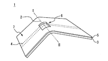
- FIG. 3 is a perspective view showing a flexible substrate according to the first embodiment.
- FIG. 2 is a sectional view taken along line I-II of FIG. 1.
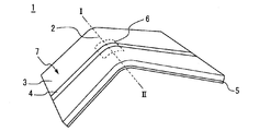
- 3 is a perspective view showing a state in which the flexible board according to Embodiment 1 is bent.
- FIG. 3 is a perspective view showing a state in which the flexible board according to Embodiment 1 is bent.
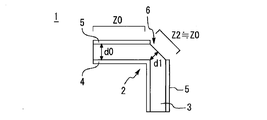
- FIG. It is sectional drawing which expanded the bending part of FIG.
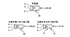
- FIG. 3 is an enlarged cross-sectional view of a flat portion and a bent portion of the flexible board according to the first embodiment. It is sectional drawing which expanded the bending part of the flexible substrate which concerns on a comparative example. It is sectional drawing which expanded the bending part of the flexible substrate which concerns on a comparative example.
- FIG. 6 is a perspective view showing a flexible substrate according to a second embodiment.
- FIG. 10 is a cross-sectional view taken along the line I-II of the flexible substrate of FIG. 9 in a bent state.
- FIG. 10 is a cross-sectional view taken along the line III-IV of the flexible substrate of FIG. 9 in a flat state.
- FIG. 9 is a perspective view showing a flexible substrate according to a third embodiment.
- FIG. 13 is a cross-sectional view taken along the line I-II in a state where the flexible substrate of FIG. 12 is bent.
- FIG. 13 is a cross-sectional view taken along line III-IV of the flexible substrate of FIG. 12 in a flat state.
- FIG. 11 is a perspective view showing a modified example of the flexible board according to the third embodiment.
- FIG. 17 is a sectional view taken along the line I-II in FIG. 16. It is sectional drawing which expanded the bending part in the state which bent the flexible substrate which concerns on Embodiment 4. It is a perspective view which shows the flexible substrate which concerns on Embodiment 5.
- FIG. 1 is a perspective view showing a flexible substrate according to the first embodiment.
- FIG. 2 is a sectional view taken along line I-II of FIG.
- the flexible substrate 1 is used to electrically connect, for example, a transceiver module package for optical communication and a host system. Although the flexible substrate 1 is bent at the bending portion 2 along I-II, FIGS. 1 and 2 show a state where it is not bent.
- the dielectric plate 3 has first and second main surfaces opposite to each other.
- the high frequency signal line 4 is provided on the first main surface of the dielectric plate 3.
- the ground conductor 5 is provided on the second main surface of the dielectric plate 3.
- the high frequency signal line 4 and the ground conductor 5 form a microstrip line.
- the ground conductor 5 is provided with a local defective portion 6 facing the high-frequency signal line 4 only at the bent portion 2.
- the defective portion 6 has a structure in which the ground conductor 5 is broken like a window. When there are a plurality of bent portions 2, one defective portion 6 is provided for each bent portion 2.
- FIG. 3 and 4 are perspective views showing a state in which the flexible board according to the first embodiment is folded.
- FIG. 5 is an enlarged sectional view of the bent portion of FIG.
- FIG. 3 shows a case where the ground conductor 5 side is convexly bent
- FIG. 4 shows a case where the high frequency signal line 4 side is convexly bent.
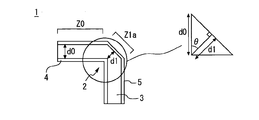
- the thickness of the dielectric plate 3 becomes thin. If the thickness of the dielectric plate 3 in the flat portion 7 of the flexible substrate 1 is d0 and the thickness of the dielectric plate 3 that is the thinnest in the bent portion 2 of the flexible substrate 1 bent at 90 ° is d1, d0> d1.
- FIG. 6 is an enlarged sectional view of a flat portion and a bent portion of the flexible board according to the first embodiment.
- the capacitance of the MIM (metal-insulator-metal) structure is proportional to the area of the conductor and inversely proportional to the thickness of the dielectric.
- the capacitance is different between the flat portion 7 and the bent portion 2 having no defective portion 6.
- the characteristic impedance of the high-frequency signal line 4 in the flat part 7 is Z0.
- the characteristic impedance of the high-frequency signal line 4 in the bent portion 2 of the bent flexible substrate 1 is Z1 when there is no defective portion 6 and Z2 when there is a defective portion 6.
- the characteristic impedance Z
- the inductance of the high-frequency signal line 4 L
- the capacitance between the high-frequency signal line 4 and the ground conductor 5 is C
- Z ⁇ (L / C)
- the discontinuity between the characteristic impedance of the flat portion 7 and the characteristic impedance of the bent portion 2 of the flexible substrate 1 can be eliminated by providing the defective portion 6.
- the dimension of the defective portion 6 needs to be selected as an optimum value according to the amount of change in the thickness of the dielectric plate 3 due to bending, the relative permittivity of the dielectric plate 3, the bending angle, the frequency of the propagating high frequency signal, and the like. There is.
- FIG. 7 and 8 are enlarged cross-sectional views of the bent portion of the flexible board according to the comparative example.
- FIG. 7 shows a case where the ground conductor 5 side is convexly bent
- FIG. 8 shows a case where the high frequency signal line 4 side is convexly bent.
- the comparative example does not have the defect portion 6.
- d1 / d0 cos ⁇ .
- ⁇ 45 °
- the characteristic impedances Z1a and Z2b of the bent portion 2 in FIGS. 7 and 8 are Z1a ⁇ Z2b ⁇ 35.5 ⁇ .
- the characteristic impedance Z0 of the flat portion 7 is normally designed to be 50 ⁇ , whereas it is 50 ⁇ or less in the bent portion 2 of the comparative example. Therefore, in the comparative example, discontinuity of the characteristic impedance occurs, RF reflection occurs, and the passage loss increases.
- the ground conductor 5 is provided with the local defect portion 6 facing the high-frequency signal line 4 only at the bent portion 2.
- the defective portion 6 compensates for the local change in the characteristic impedance of the bent portion 2 with respect to the characteristic impedance of the flat portion 7 of the flexible substrate 1. Therefore, the discontinuity between the characteristic impedance of the flat portion 7 and the characteristic impedance of the bent portion 2 of the flexible substrate 1 can be eliminated.
- the reflection of the signal can be reduced and the passage loss can be reduced, so that the high frequency signal of the transceiver module for optical communication can be propagated stably and efficiently.
- one high-frequency signal line 4 is provided on the flexible substrate 1, but the high-frequency signal line 4 may be plural or may be mixed with the DC line.
- the flexible substrate 1 is not limited to a single layer structure and may have a multilayer structure. There may be a plurality of bent portions 2, and the bent portions 2 whose bending directions are opposite may be mixed.
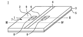
- FIG. 9 is a perspective view showing a flexible substrate according to the second embodiment.
- FIG. 10 is a sectional view taken along the line I-II of the flexible substrate of FIG. 9 in a bent state.
- FIG. 11 is a cross-sectional view taken along line III-IV of the flexible substrate of FIG.
- the width of the high-frequency signal line 4 is locally narrowed only in the bent portion 2 along I-II.
- the thickness d1 of the dielectric plate 3 of the bent portion 2 when the flexible substrate 1 is bent is smaller than the thickness d0 of the dielectric plate 3 of the flat portion 7 (d1 ⁇ d0). Therefore, the capacitance C1 between the high-frequency signal line 4 and the ground conductor 5 in the bent portion 2 becomes larger than the capacitance C0 in the flat portion 7 (C1> C0).
- Characteristic impedance is determined by the ratio of capacitance and inductance L.
- the inductance L corresponds to the line width of the high frequency signal line 4. Therefore, in the present embodiment, the width w1 of the high-frequency signal line 4 in the bent portion 2 is locally narrower than the width w0 in the flat portion 7 (w1 ⁇ w0).
- the inductance L1 of the bent portion 2 becomes larger than the inductance L0 of the flat portion 7 (L1> L0).
- the discontinuity between the characteristic impedance Z0 of the flat portion 7 of the flexible substrate 1 and the characteristic impedance Z1 of the bent portion 2 can be eliminated (Z1 ⁇ Z0).
- the width w1 of the high-frequency signal line 4 in the bent portion 2 is optimal according to the amount of change in the thickness of the dielectric plate 3 due to bending, the relative permittivity of the dielectric plate 3, the bending angle, the frequency of the propagating high-frequency signal, and the like. You need to select a different value.
- FIG. 12 is a perspective view showing a flexible substrate according to the third embodiment.
- FIG. 13 is a cross-sectional view taken along the line I-II in a state where the flexible substrate of FIG. 12 is bent.
- FIG. 14 is a cross-sectional view taken along line III-IV of the flexible substrate of FIG.
- the ground conductor 5 is provided with a local defect portion 6 facing the high-frequency signal line 4 only at the bent portion 2.
- the ground conductor 8 is locally provided on the side of the high-frequency signal line 4 only in the bent portion 2.
- the ground conductor 5 and the ground conductor 8 are electrically connected to each other via a via 9 penetrating the dielectric plate 3.
- the high frequency signal line 4 and the ground conductor 5 form a microstrip line.
- the high frequency signal line 4 and the ground conductor 8 form a coplanar line.
- the thickness of the dielectric plate 3 is thin in the bent portion 2, but since the defective portion 6 is provided, the characteristic impedance of the bent portion 2 can ignore the influence of the thickness of the dielectric plate 3.
- the characteristic impedance Z3 of the bent portion 2 forming the coplanar line is determined by the width w3 of the high frequency signal line 4 of the planar line, the distance s3 between the high frequency signal line 4 and the ground conductor 8 and the dielectric constant of the dielectric plate 3. Note that the surface layer portion is dominant in the influence of the dielectric constant of the dielectric plate 3.
- the distance s3 between the high-frequency signal line 4 and the ground conductor 8 is made sufficiently smaller than the distance between the high-frequency signal line 4 and the ground conductor 5. This compensates for the local change in the characteristic impedance of the bent portion 2 with respect to the characteristic impedance of the flat portion 7 of the flexible substrate 1. Therefore, the discontinuity between the characteristic impedance of the flat portion 7 and the characteristic impedance of the bent portion 2 of the flexible substrate 1 can be eliminated.
- the bent shape can be easily maintained by providing the ground conductor 8. Therefore, the high frequency characteristics can be stabilized against the stress on the flexible substrate 1 due to the external force or the temperature change at the time of installation.
- the size of the missing portion 6, the width w3 of the high-frequency signal line 4 of the coplanar line, the distance s3 between the high-frequency signal line 4 and the ground conductor 8, and the like are the amount of change in the thickness of the dielectric plate 3 due to bending, It is necessary to select the optimum value according to the relative permittivity, the bending angle, the frequency of the propagating high frequency signal, and the like.
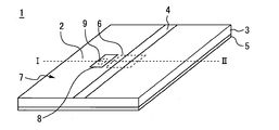
- FIG. 15 is a perspective view showing a modification of the flexible board according to the third embodiment.
- the ground conductor 8 forming the coplanar line is provided only on one side of the high-frequency signal line 4.
- a plurality of high-frequency signal lines 4 may be provided in a limited space in actual wiring. In such a case, by providing the ground conductor 8 only on one side of the high-frequency signal line 4, it is possible to save space and reduce restrictions on the arrangement of other wiring.
- Other configurations and effects are similar to those of the third embodiment.
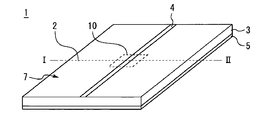
- FIG. 16 is a perspective view showing a flexible board according to the fourth embodiment.
- FIG. 17 is a sectional view taken along line I-II of FIG.
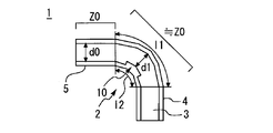
- FIG. 18 is an enlarged cross-sectional view of the bent portion of the flexible board according to the fourth embodiment in a bent state.
- a local recess 10 is provided on the second main surface of the dielectric plate 3 so as to face the high-frequency signal line 4 only at the bent portion 2.
- the ground conductor 5 is embedded in the recess 10.
- the length l1 of the high-frequency signal line 4 on the outer side of the bent portion 2 greatly extends with respect to the length l2 of the ground conductor 5 on the inner side of the bent portion 2.
- the steepness of the bent portion 2 is small and the bent region of the bent portion 2 is relatively wide, the influence of the extension of the high-frequency signal line 4 on the characteristic impedance is greater than the influence of the thin thickness of the dielectric plate 3. .. Therefore, the increased inductance in the bent portion 2 may increase the characteristic impedance.
- the bent portion 2 is provided with the concave portion 10 and is embedded with the ground conductor 5.
- the distance between the high-frequency signal line 4 and the ground conductor 5 is shortened at the bent portion 2, and the capacitance is increased.
- This structure compensates for the local change in the characteristic impedance of the bent portion 2 with respect to the characteristic impedance of the flat portion 7 of the flexible substrate 1. Therefore, the discontinuity between the characteristic impedance of the flat portion 7 and the characteristic impedance of the bent portion 2 of the flexible substrate 1 can be eliminated.
- the depth, size, etc. of the recess 10 are determined by the extension (11-12) of the high-frequency signal line 4 by bending, the amount of change in the thickness of the dielectric plate 3 due to bending, the relative permittivity of the dielectric plate 3, and the bending angle. It is necessary to select the optimum value according to the frequency of the propagating high frequency signal.
- FIG. 19 is a perspective view showing a flexible substrate according to the fifth embodiment.
- a dielectric 11 having a dielectric constant different from that of the dielectric plate 3 is locally embedded in the dielectric plate 3 only in the bent portion 2 in a region facing the high-frequency signal line 4.
- the second main surface of the dielectric plate 3 provided with the ground conductor 5 is dug in to embed the dielectric 11, but the first main surface provided with the high-frequency signal line 4 is dug into the dielectric 11. May be embedded.
- a material having a relative dielectric constant smaller than that of the dielectric plate 3 is selected as the material of the dielectric 11.
- a material having a relative dielectric constant larger than that of the dielectric plate 3 is selected as the material of the dielectric 11.
- the relative permittivity of the dielectric body 11, the embedded depth of the dielectric body 11, the size of the dielectric body 11, and the like are the amount of change in the thickness of the dielectric plate 3 due to bending, the relative permittivity of the dielectric plate 3, the bending angle, and the propagation. It is necessary to select an optimum value according to the frequency of the high frequency signal to be used.
Landscapes
- Engineering & Computer Science (AREA)
- Microelectronics & Electronic Packaging (AREA)
- Physics & Mathematics (AREA)
- Electromagnetism (AREA)
- Structure Of Printed Boards (AREA)
- Waveguides (AREA)
Abstract
Description
図1は、実施の形態1に係るフレキシブル基板を示す斜視図である。図2は図1のI-IIに沿った断面図である。フレキシブル基板1は例えば光通信用送受信モジュールパッケージと上位システムとを電気的に接続するために用いられる。フレキシブル基板1は、I-IIに沿った折り曲げ部2で折り曲げられるが、図1,2では折り曲げていない状態を示している。
図9は、実施の形態2に係るフレキシブル基板を示す斜視図である。図10は図9のフレキシブル基板が折り曲げられた状態のI-IIに沿った断面図である。図11は図9のフレキシブル基板が平坦な状態のIII-IVに沿った断面図である。I-IIに沿った折り曲げ部2のみにおいて高周波信号線路4の幅が局所的に狭くなっている。
図12は、実施の形態3に係るフレキシブル基板を示す斜視図である。図13は図12のフレキシブル基板が折り曲げられた状態のI-IIに沿った断面図である。図14は図12のフレキシブル基板が平坦な状態のIII-IVに沿った断面図である。
図16は、実施の形態4に係るフレキシブル基板を示す斜視図である。図17は図16のI-IIに沿った断面図である。図18は、実施の形態4に係るフレキシブル基板を折り曲げた状態の折り曲げ部を拡大した断面図である。誘電体板3の第2の主面には、折り曲げ部2のみにおいて高周波信号線路4に対向して局所的な凹部10が設けられている。凹部10にグランド導体5が埋め込まれている。
図19は、実施の形態5に係るフレキシブル基板を示す斜視図である。誘電体板3の誘電率とは異なる誘電率を持つ誘電体11が高周波信号線路4に対向する領域において折り曲げ部2のみに局所的に誘電体板3に埋め込まれている。グランド導体5が設けられた誘電体板3の第2の主面を掘り込んで誘電体11を埋め込んでいるが、高周波信号線路4が設けられた第1の主面を掘り込んで誘電体11を埋め込んでもよい。
Claims (7)
- 折り曲げ部で折り曲げられるフレキシブル基板であって、
互いに反対側の第1及び第2の主面を持つ誘電体板と、
前記誘電体板の前記第1の主面に設けられた高周波信号線路と、
前記誘電体板の前記第2の主面に設けられたグランド導体とを備え、
前記高周波信号線路と前記グランド導体がマイクロストリップ線路を構成し、
前記グランド導体には、前記折り曲げ部のみにおいて前記高周波信号線路に対向して局所的な欠損部が設けられていることを特徴とするフレキシブル基板。 - 折り曲げ部で折り曲げられるフレキシブル基板であって、
互いに反対側の第1及び第2の主面を持つ誘電体板と、
前記誘電体板の前記第1の主面に設けられた高周波信号線路と、
前記誘電体板の前記第2の主面に設けられたグランド導体とを備え、
前記高周波信号線路と前記グランド導体がマイクロストリップ線路を構成し、
前記折り曲げ部のみにおいて前記高周波信号線路の幅が局所的に狭くなっていることを特徴とするフレキシブル基板。 - 折り曲げ部で折り曲げられるフレキシブル基板であって、
互いに反対側の第1及び第2の主面を持つ誘電体板と、
前記誘電体板の前記第1の主面に設けられた高周波信号線路と、
前記誘電体板の前記第2の主面に設けられた第1のグランド導体と、
前記折り曲げ部のみにおいて前記高周波信号線路のサイドに局所的に設けられた第2のグランド導体とを備え、
前記高周波信号線路と前記第1のグランド導体がマイクロストリップ線路を構成し、
前記高周波信号線路と前記第2のグランド導体がコプレーナ線路を構成し、
前記第1のグランド導体には、前記折り曲げ部のみにおいて前記高周波信号線路に対向して局所的な欠損部が設けられ、
前記高周波信号線路と前記第2のグランド導体との間の距離が前記高周波信号線路と前記第1のグランド導体との距離よりも小さいことを特徴とするフレキシブル基板。 - 前記第2のグランド導体が前記高周波信号線路の片側のみに設けられていることを特徴とする請求項3に記載のフレキシブル基板。
- 折り曲げ部で折り曲げられるフレキシブル基板であって、
互いに反対側の第1及び第2の主面を持つ誘電体板と、
前記誘電体板の前記第1の主面に設けられた高周波信号線路と、
前記誘電体板の前記第2の主面に設けられたグランド導体とを備え、
前記高周波信号線路と前記グランド導体がマイクロストリップ線路を構成し、
前記誘電体板の前記第2の主面には、前記折り曲げ部のみにおいて前記高周波信号線路に対向して局所的な凹部が設けられ、
前記凹部に前記グランド導体が埋め込まれていることを特徴とするフレキシブル基板。 - 折り曲げ部で折り曲げられるフレキシブル基板であって、
互いに反対側の第1及び第2の主面を持つ誘電体板と、
前記誘電体板の前記第1の主面に設けられた高周波信号線路と、
前記誘電体板の前記第2の主面に設けられたグランド導体と、
前記折り曲げ部のみにおいて前記高周波信号線路に対向して局所的に前記誘電体板に埋め込まれ、前記誘電体板の誘電率とは異なる誘電率を持つ誘電体とを備え、
前記高周波信号線路と前記グランド導体がマイクロストリップ線路を構成することを特徴とするフレキシブル基板。 - 前記フレキシブル基板の平坦部の特性インピーダンスに対する前記折り曲げ部の局所的な特性インピーダンスの変化が補償されていることを特徴とする請求項1~6の何れか1項に記載のフレキシブル基板。
Priority Applications (6)
| Application Number | Priority Date | Filing Date | Title |
|---|---|---|---|
| JP2019518327A JP6620911B1 (ja) | 2018-11-22 | 2018-11-22 | フレキシブル基板 |
| CN201880096727.0A CN112997586B (zh) | 2018-11-22 | 2018-11-22 | 柔性基板 |
| PCT/JP2018/043238 WO2020105181A1 (ja) | 2018-11-22 | 2018-11-22 | フレキシブル基板 |
| DE112018008161.3T DE112018008161T5 (de) | 2018-11-22 | 2018-11-22 | Flexibles Substrat |
| KR1020217013945A KR102578352B1 (ko) | 2018-11-22 | 2018-11-22 | 플렉시블 기판 |
| US17/258,366 US11431070B2 (en) | 2018-11-22 | 2018-11-22 | Flexible substrate |
Applications Claiming Priority (1)
| Application Number | Priority Date | Filing Date | Title |
|---|---|---|---|
| PCT/JP2018/043238 WO2020105181A1 (ja) | 2018-11-22 | 2018-11-22 | フレキシブル基板 |
Publications (1)
| Publication Number | Publication Date |
|---|---|
| WO2020105181A1 true WO2020105181A1 (ja) | 2020-05-28 |
Family
ID=68917258
Family Applications (1)
| Application Number | Title | Priority Date | Filing Date |
|---|---|---|---|
| PCT/JP2018/043238 Ceased WO2020105181A1 (ja) | 2018-11-22 | 2018-11-22 | フレキシブル基板 |
Country Status (6)
| Country | Link |
|---|---|
| US (1) | US11431070B2 (ja) |
| JP (1) | JP6620911B1 (ja) |
| KR (1) | KR102578352B1 (ja) |
| CN (1) | CN112997586B (ja) |
| DE (1) | DE112018008161T5 (ja) |
| WO (1) | WO2020105181A1 (ja) |
Cited By (1)
| Publication number | Priority date | Publication date | Assignee | Title |
|---|---|---|---|---|
| JP2024025484A (ja) * | 2022-08-12 | 2024-02-26 | 新光電気工業株式会社 | 配線基板、半導体装置 |
Families Citing this family (6)
| Publication number | Priority date | Publication date | Assignee | Title |
|---|---|---|---|---|
| JP6773259B1 (ja) * | 2019-02-20 | 2020-10-21 | 株式会社村田製作所 | アンテナモジュールおよびそれを搭載した通信装置、ならびにアンテナモジュールの製造方法 |
| EP4329438A4 (en) | 2021-08-05 | 2025-01-15 | Samsung Electronics Co., Ltd. | FLEXIBLE CONNECTING ELEMENT AND ELECTRONIC DEVICE THEREFOR |
| KR20230021466A (ko) * | 2021-08-05 | 2023-02-14 | 삼성전자주식회사 | 플렉서블 접속 부재 및 그를 포함하는 전자 장치 |
| CN113709993B (zh) * | 2021-08-27 | 2023-06-27 | 博敏电子股份有限公司 | 一种动态阻抗产品的制作方法 |
| CN116935742B (zh) * | 2022-03-30 | 2025-11-07 | 华为技术有限公司 | 一种折叠屏辅助装置及其制作方法和相关设备 |
| WO2026022516A1 (en) * | 2024-07-25 | 2026-01-29 | Telefonaktiebolaget Lm Ericsson (Publ) | Millimeter wave frasera (mmf) radiator with integrated broadside coupled transmission line |
Citations (7)
| Publication number | Priority date | Publication date | Assignee | Title |
|---|---|---|---|---|
| JPH0422075A (ja) * | 1990-05-17 | 1992-01-27 | Seiko Epson Corp | 配線接続装置 |
| JPH0568102U (ja) * | 1992-02-18 | 1993-09-10 | 株式会社東芝 | 積層基板 |
| JP2000091801A (ja) * | 1998-09-10 | 2000-03-31 | Toshiba Corp | 接続線路基板 |
| JP2007129111A (ja) * | 2005-11-04 | 2007-05-24 | Jisedai Gijutsu:Kk | 立体基板 |
| JP2012227632A (ja) * | 2011-04-18 | 2012-11-15 | Murata Mfg Co Ltd | 高周波伝送線路およびアンテナ装置 |
| WO2013094471A1 (ja) * | 2011-12-22 | 2013-06-27 | 株式会社村田製作所 | 高周波信号線路及び電子機器 |
| WO2014156422A1 (ja) * | 2013-03-26 | 2014-10-02 | 株式会社村田製作所 | 樹脂多層基板および電子機器 |
Family Cites Families (9)
| Publication number | Priority date | Publication date | Assignee | Title |
|---|---|---|---|---|
| JPS54144273A (en) * | 1978-04-29 | 1979-11-10 | Sadayasu Eguchi | Wreath |
| JP2007123740A (ja) | 2005-10-31 | 2007-05-17 | Sony Corp | フレキシブル基板、光送受信モジュール及び光送受信装置 |
| JP5344736B2 (ja) * | 2008-02-20 | 2013-11-20 | 太陽誘電株式会社 | 基材、通信モジュール、および通信装置 |
| JP5041108B2 (ja) | 2010-12-03 | 2012-10-03 | 株式会社村田製作所 | 高周波信号線路 |
| KR101454720B1 (ko) * | 2010-12-03 | 2014-10-27 | 가부시키가이샤 무라타 세이사쿠쇼 | 고주파 신호선로 및 전자기기 |
| WO2013069763A1 (ja) | 2011-11-10 | 2013-05-16 | 株式会社村田製作所 | 高周波信号線路及びこれを備えた電子機器 |
| JP2014086655A (ja) * | 2012-10-26 | 2014-05-12 | Murata Mfg Co Ltd | フレキシブル基板 |
| WO2015005028A1 (ja) * | 2013-07-09 | 2015-01-15 | 株式会社村田製作所 | 高周波伝送線路 |
| JP2017028500A (ja) * | 2015-07-22 | 2017-02-02 | ホシデン株式会社 | フレキシブル配線基板 |
-
2018
- 2018-11-22 KR KR1020217013945A patent/KR102578352B1/ko active Active
- 2018-11-22 JP JP2019518327A patent/JP6620911B1/ja active Active
- 2018-11-22 CN CN201880096727.0A patent/CN112997586B/zh active Active
- 2018-11-22 US US17/258,366 patent/US11431070B2/en active Active
- 2018-11-22 WO PCT/JP2018/043238 patent/WO2020105181A1/ja not_active Ceased
- 2018-11-22 DE DE112018008161.3T patent/DE112018008161T5/de not_active Withdrawn
Patent Citations (7)
| Publication number | Priority date | Publication date | Assignee | Title |
|---|---|---|---|---|
| JPH0422075A (ja) * | 1990-05-17 | 1992-01-27 | Seiko Epson Corp | 配線接続装置 |
| JPH0568102U (ja) * | 1992-02-18 | 1993-09-10 | 株式会社東芝 | 積層基板 |
| JP2000091801A (ja) * | 1998-09-10 | 2000-03-31 | Toshiba Corp | 接続線路基板 |
| JP2007129111A (ja) * | 2005-11-04 | 2007-05-24 | Jisedai Gijutsu:Kk | 立体基板 |
| JP2012227632A (ja) * | 2011-04-18 | 2012-11-15 | Murata Mfg Co Ltd | 高周波伝送線路およびアンテナ装置 |
| WO2013094471A1 (ja) * | 2011-12-22 | 2013-06-27 | 株式会社村田製作所 | 高周波信号線路及び電子機器 |
| WO2014156422A1 (ja) * | 2013-03-26 | 2014-10-02 | 株式会社村田製作所 | 樹脂多層基板および電子機器 |
Cited By (1)
| Publication number | Priority date | Publication date | Assignee | Title |
|---|---|---|---|---|
| JP2024025484A (ja) * | 2022-08-12 | 2024-02-26 | 新光電気工業株式会社 | 配線基板、半導体装置 |
Also Published As
| Publication number | Publication date |
|---|---|
| KR102578352B1 (ko) | 2023-09-13 |
| DE112018008161T5 (de) | 2021-08-05 |
| JPWO2020105181A1 (ja) | 2021-02-15 |
| KR20210070362A (ko) | 2021-06-14 |
| CN112997586B (zh) | 2024-05-28 |
| CN112997586A (zh) | 2021-06-18 |
| US20210296750A1 (en) | 2021-09-23 |
| JP6620911B1 (ja) | 2019-12-18 |
| US11431070B2 (en) | 2022-08-30 |
Similar Documents
| Publication | Publication Date | Title |
|---|---|---|
| WO2020105181A1 (ja) | フレキシブル基板 | |
| JP3241019B2 (ja) | コプレーナ線路 | |
| US7884682B2 (en) | Waveguide to microstrip transducer having a ridge waveguide and an impedance matching box | |
| EP1304762B1 (en) | Transmission line to waveguide transition structures | |
| US7193490B2 (en) | High frequency transmission line and high frequency board | |
| US11909088B2 (en) | Transmission line member including first and third transmission line portions connected by a second coplanar waveguide portion of reduced thickness and greater width | |
| US20190341666A1 (en) | Vertical transition method applied between coaxial structure and microstrip line | |
| WO2009123233A1 (ja) | 高周波モジュールおよびその製造方法ならびに該高周波モジュールを備えた送信器、受信器、送受信器およびレーダ装置 | |
| JP6907918B2 (ja) | コネクタおよびコネクタ平面線路接続構造 | |
| CN1860650A (zh) | 连接同轴传输线与共面传输线的装置 | |
| US11011814B2 (en) | Coupling comprising a conductive wire embedded in a post-wall waveguide and extending into a hollow tube waveguide | |
| JP6937965B2 (ja) | 高周波回路及び通信モジュール | |
| US11335987B2 (en) | Directional coupler | |
| JP2005051330A (ja) | 誘電体導波管線路と高周波伝送線路との接続構造およびそれを用いた高周波回路基板ならびに高周波素子搭載用パッケージ | |
| JP7077137B2 (ja) | 伝送線路およびコネクタ | |
| US5160904A (en) | Microstrip circuit with transition for different dielectric materials | |
| US9118301B2 (en) | Bonding wire impedance matching circuit | |
| US20110241803A1 (en) | Signal transmission line | |
| US12120820B2 (en) | Electronic device | |
| JPH10256801A (ja) | マイクロ波回路 | |
| JP2001053511A (ja) | 高周波用配線基板および接続構造 | |
| WO2022219709A1 (ja) | 配線基板 | |
| JP4203405B2 (ja) | 導波管構造体の分岐構造およびアンテナ基板 | |
| JP2001298306A (ja) | 高周波伝送線路基板、及び高周波パッケージ | |
| JP3972045B2 (ja) | 積層型ランゲカプラ |
Legal Events
| Date | Code | Title | Description |
|---|---|---|---|
| ENP | Entry into the national phase |
Ref document number: 2019518327 Country of ref document: JP Kind code of ref document: A |
|
| 121 | Ep: the epo has been informed by wipo that ep was designated in this application |
Ref document number: 18940615 Country of ref document: EP Kind code of ref document: A1 |
|
| ENP | Entry into the national phase |
Ref document number: 20217013945 Country of ref document: KR Kind code of ref document: A |
|
| 122 | Ep: pct application non-entry in european phase |
Ref document number: 18940615 Country of ref document: EP Kind code of ref document: A1 |