WO2020105172A1 - 無停電電源装置 - Google Patents
無停電電源装置Info
- Publication number
- WO2020105172A1 WO2020105172A1 PCT/JP2018/043195 JP2018043195W WO2020105172A1 WO 2020105172 A1 WO2020105172 A1 WO 2020105172A1 JP 2018043195 W JP2018043195 W JP 2018043195W WO 2020105172 A1 WO2020105172 A1 WO 2020105172A1
- Authority
- WO
- WIPO (PCT)
- Prior art keywords
- voltage
- power supply
- phase
- reference voltage
- capacitor
- Prior art date
- Legal status (The legal status is an assumption and is not a legal conclusion. Google has not performed a legal analysis and makes no representation as to the accuracy of the status listed.)
- Ceased
Links
Images





Classifications
-
- H—ELECTRICITY
- H02—GENERATION; CONVERSION OR DISTRIBUTION OF ELECTRIC POWER
- H02J—ELECTRIC POWER NETWORKS; CIRCUIT ARRANGEMENTS OR SYSTEMS FOR SUPPLYING OR DISTRIBUTING ELECTRIC POWER; SYSTEMS FOR STORING ELECTRIC ENERGY
- H02J9/00—Circuit arrangements for emergency or stand-by power supply, e.g. for emergency lighting
- H02J9/04—Circuit arrangements for emergency or stand-by power supply, e.g. for emergency lighting in which the distribution system is disconnected from the normal source and connected to a standby source
- H02J9/06—Circuit arrangements for emergency or stand-by power supply, e.g. for emergency lighting in which the distribution system is disconnected from the normal source and connected to a standby source with automatic change-over, e.g. UPS systems
- H02J9/061—Circuit arrangements for emergency or stand-by power supply, e.g. for emergency lighting in which the distribution system is disconnected from the normal source and connected to a standby source with automatic change-over, e.g. UPS systems for DC powered loads
-
- H—ELECTRICITY
- H02—GENERATION; CONVERSION OR DISTRIBUTION OF ELECTRIC POWER
- H02J—ELECTRIC POWER NETWORKS; CIRCUIT ARRANGEMENTS OR SYSTEMS FOR SUPPLYING OR DISTRIBUTING ELECTRIC POWER; SYSTEMS FOR STORING ELECTRIC ENERGY
- H02J9/00—Circuit arrangements for emergency or stand-by power supply, e.g. for emergency lighting
- H02J9/04—Circuit arrangements for emergency or stand-by power supply, e.g. for emergency lighting in which the distribution system is disconnected from the normal source and connected to a standby source
- H02J9/06—Circuit arrangements for emergency or stand-by power supply, e.g. for emergency lighting in which the distribution system is disconnected from the normal source and connected to a standby source with automatic change-over, e.g. UPS systems
- H02J9/062—Circuit arrangements for emergency or stand-by power supply, e.g. for emergency lighting in which the distribution system is disconnected from the normal source and connected to a standby source with automatic change-over, e.g. UPS systems for AC powered loads
-
- H—ELECTRICITY
- H02—GENERATION; CONVERSION OR DISTRIBUTION OF ELECTRIC POWER
- H02J—ELECTRIC POWER NETWORKS; CIRCUIT ARRANGEMENTS OR SYSTEMS FOR SUPPLYING OR DISTRIBUTING ELECTRIC POWER; SYSTEMS FOR STORING ELECTRIC ENERGY
- H02J9/00—Circuit arrangements for emergency or stand-by power supply, e.g. for emergency lighting
- H02J9/04—Circuit arrangements for emergency or stand-by power supply, e.g. for emergency lighting in which the distribution system is disconnected from the normal source and connected to a standby source
- H02J9/06—Circuit arrangements for emergency or stand-by power supply, e.g. for emergency lighting in which the distribution system is disconnected from the normal source and connected to a standby source with automatic change-over, e.g. UPS systems
- H02J9/068—Electronic means for switching from one power supply to another power supply, e.g. to avoid parallel connection
-
- H—ELECTRICITY
- H02—GENERATION; CONVERSION OR DISTRIBUTION OF ELECTRIC POWER
- H02M—APPARATUS FOR CONVERSION BETWEEN AC AND AC, BETWEEN AC AND DC, OR BETWEEN DC AND DC, AND FOR USE WITH MAINS OR SIMILAR POWER SUPPLY SYSTEMS; CONVERSION OF DC OR AC INPUT POWER INTO SURGE OUTPUT POWER; CONTROL OR REGULATION THEREOF
- H02M1/00—Details of apparatus for conversion
- H02M1/14—Arrangements for reducing ripples from DC input or output
-
- H—ELECTRICITY
- H02—GENERATION; CONVERSION OR DISTRIBUTION OF ELECTRIC POWER
- H02M—APPARATUS FOR CONVERSION BETWEEN AC AND AC, BETWEEN AC AND DC, OR BETWEEN DC AND DC, AND FOR USE WITH MAINS OR SIMILAR POWER SUPPLY SYSTEMS; CONVERSION OF DC OR AC INPUT POWER INTO SURGE OUTPUT POWER; CONTROL OR REGULATION THEREOF
- H02M7/00—Conversion of AC power input into DC power output; Conversion of DC power input into AC power output
- H02M7/02—Conversion of AC power input into DC power output without possibility of reversal
- H02M7/04—Conversion of AC power input into DC power output without possibility of reversal by static converters
-
- H—ELECTRICITY
- H02—GENERATION; CONVERSION OR DISTRIBUTION OF ELECTRIC POWER
- H02M—APPARATUS FOR CONVERSION BETWEEN AC AND AC, BETWEEN AC AND DC, OR BETWEEN DC AND DC, AND FOR USE WITH MAINS OR SIMILAR POWER SUPPLY SYSTEMS; CONVERSION OF DC OR AC INPUT POWER INTO SURGE OUTPUT POWER; CONTROL OR REGULATION THEREOF
- H02M7/00—Conversion of AC power input into DC power output; Conversion of DC power input into AC power output
- H02M7/42—Conversion of DC power input into AC power output without possibility of reversal
- H02M7/44—Conversion of DC power input into AC power output without possibility of reversal by static converters
Definitions
- the present invention relates to an uninterruptible power supply, and particularly to an inverter power supply mode in which AC power is supplied from an inverter to a load, a bypass power supply mode in which AC power is supplied to a load from a bypass AC power supply, and a load is supplied from both the inverter and the bypass AC power supply.
- the present invention relates to an uninterruptible power supply having a lap power supply mode for supplying AC power to a power supply.
- Patent Document 1 discloses an uninterruptible power supply device having an inverter power supply mode, a bypass power supply mode, and a lap power supply mode.
- This uninterruptible power supply includes a converter that converts an AC voltage supplied from a commercial AC power supply into a DC voltage, a capacitor that smoothes a DC output voltage of the converter, and an inverter that converts a voltage between terminals of the capacitor into an AC voltage.
- a first switch whose one terminal receives the AC output voltage of the inverter and whose other terminal is connected to the load; and one terminal which receives the AC voltage supplied from the bypass AC power supply and whose other terminal is connected to the load. And two switches.
- the first switch In the inverter power supply mode, the first switch is turned on and the second switch is turned off. In the bypass power feeding mode, the second switch is turned on and the first switch is turned off. In the lap power supply mode, both the first and second switches are turned on. The lap power supply mode is executed during a switching period for switching between the inverter power supply mode and the bypass power supply mode.
- each of the commercial AC power supply and the bypass AC power supply includes a three-phase AC power supply star-connected to the neutral point, and the commercial AC power supply and the bypass AC power supply are neutral. If both points are grounded, a circulating current may flow from one of the commercial AC power supply and the bypass AC power supply to the other AC power supply through the capacitor in the lap power supply mode (Fig. 6, see FIG. 7).
- a large circulating current flows, an overcurrent is detected, or an overvoltage of the capacitor is detected, so that the operation of the uninterruptible power supply is stopped and the operation of the load is stopped.
- a main object of the present invention is to provide an uninterruptible power supply capable of preventing a circulating current from flowing even when the neutral points of the first and second AC power supplies are grounded. is there.
- the uninterruptible power supply includes a forward converter, a capacitor, an inverse converter, a first switch, a second switch, a first controller, and a second controller. ..
- the forward converter converts the three-phase AC voltage supplied from the first AC power supply into a DC voltage.
- the capacitor smoothes the DC output voltage of the forward converter.
- the inverse converter converts the voltage between the terminals of the capacitor into a three-phase AC voltage.
- the first switch is provided corresponding to each phase of the three-phase AC voltage output from the inverse converter, one terminal receives the AC voltage of the corresponding phase, and the other terminal is connected to the load.
- the second switch is provided corresponding to each phase of the three-phase AC voltage supplied from the second AC power supply, one terminal receives the AC voltage of the corresponding phase, and the other terminal is connected to the load.
- the first control unit turns on the first switch and turns off the second switch in the first mode in which the three-phase AC voltage is supplied from the inverse converter to the load.
- the first control unit turns on the second switch and turns off the first switch in the second mode in which the three-phase AC voltage is supplied from the second AC power supply to the load.
- the first control unit turns on both the first and second switches to turn on the inverse converter during the switching period in which one of the first mode and the second mode is switched to the other mode.
- a third mode of supplying a three-phase AC voltage to the load from both of the second AC power supplies is executed.
- the second controller controls the forward converter so that the inter-terminal voltage of the capacitor becomes the first reference voltage in the first and second modes.
- the second control unit controls the forward converter so that the inter-terminal voltage of the capacitor becomes the second reference voltage higher than the first reference voltage during the switching period.
- the second control unit prevents a circulating current from flowing from any one of the first and second AC power supplies to the other AC power supply via the capacitor.
- the terminal voltage of the capacitor is set to the second reference voltage higher than the first reference voltage during the switching period for switching the first mode and the second mode.
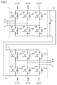
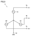
- FIG. 2 is a circuit diagram showing configurations of a converter and an inverter shown in FIG. 1. It is an equivalent circuit diagram which shows the structure of the commercial alternating current power supply shown in FIG. It is an equivalent circuit diagram which shows the structure of the bypass alternating current power supply shown in FIG.
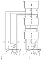
- FIG. 4 is a diagram showing the relationship between the three-phase AC voltage of the commercial AC power supply shown in FIG. 3 and the three-phase AC voltage of the bypass AC power supply. It is a circuit block diagram for explaining the effect of the invention in this application.
- FIG. 6 is another circuit block diagram for explaining the effect of the present invention.
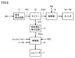
- FIG. 2 is a block diagram showing a main part of the control device shown in FIG. 1.
- FIG. 9 is a circuit block diagram showing a configuration of a control unit 15 shown in FIG. 8.
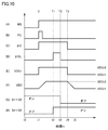
- 9 is a time chart showing the operation of the control device shown in FIG. 8.
- 9 is another time chart showing the operation of the control device shown in FIG. 8.
- FIG. 1 is a circuit block diagram showing the configuration of an uninterruptible power supply according to an embodiment of the present invention.
- this uninterruptible power supply system includes capacitors C1 to C6, Cd, reactors L1 to L6, current detectors CT1 to CT6, a converter 1, a DC positive bus Lp, a DC negative bus Ln, a bidirectional chopper 2, and an inverter 3. , Switches S1 to S6, an operation unit 4, and a control device 5.
- This uninterruptible power supply receives commercial-phase three-phase AC power from the commercial AC power supply 6 and the bypass AC power supply 7, and supplies the load 8 with commercial-frequency three-phase AC power.
- the commercial AC power supply 6 outputs three-phase AC voltages Vu1, Vv1, Vw1 to the AC output terminals 6a-6c, respectively.
- the neutral point terminal 6d of the commercial AC power supply 6 receives the ground voltage GND.
- the instantaneous values of the three-phase AC voltages Vu1, Vv1, Vw1 are detected by the control device 5.
- the control device 5 detects, based on the AC output voltages Vu1, Vv1, and Vw1 of the commercial AC power supply 6, whether or not a power failure of the commercial AC power supply 6 has occurred.
- the bypass AC power supply 7 outputs three-phase AC voltages Vu2, Vv2, Vw2 to the AC output terminals 7a to 7c, respectively.
- the neutral point terminal 7d of the bypass AC power supply 7 receives the ground voltage GND.
- the instantaneous values of the three-phase AC voltages Vu2, Vv2, Vw2 are detected by the controller 5.
- the AC input terminals 8a to 8c of the load 8 receive a three-phase AC voltage from the uninterruptible power supply.
- the load 8 is driven by the three-phase AC power supplied from the uninterruptible power supply.
- One electrodes of the capacitors C1 to C3 are connected to the AC output terminals 6a to 6c of the commercial AC power source 6, respectively, and the other electrodes thereof are connected to each other.
- Reactors L1 to L3 have one terminals connected to AC output terminals 6a to 6c of commercial AC power supply 6, respectively, and the other terminals connected to three input nodes of converter 1, respectively.
- the capacitors C1 to C3 and the reactors L1 to L3 form an AC filter F1.
- the AC filter F1 is a low-pass filter, and allows a commercial frequency AC current to flow from the commercial AC power source 6 to the converter 1 and prevents a signal having a switching frequency from flowing from the converter 1 to the commercial AC power source 6.
- the current detectors CT1 to CT3 detect the AC currents I1 to I3 flowing in the reactors L1 to L3, respectively, and give the control device 5 a signal indicating a detected value.
- the positive side output node of converter 1 is connected to the positive side input node of inverter 3 via DC positive bus Lp.
- the negative output node of converter 1 is connected to the negative input node of inverter 3 via DC negative bus Ln.
- Capacitor Cd is connected between buses Lp and Ln, and smoothes DC voltage VDC between buses Lp and Ln. The instantaneous value of DC voltage VDC is detected by control device 5.
- the converter 1 is controlled by the control device 5, and when the three-phase AC power is normally supplied from the commercial AC power supply 6 (when the commercial AC power supply 6 is healthy), the three-phase AC power from the commercial AC power supply 6 is supplied. To DC power.
- the DC power generated by converter 1 is supplied to bidirectional chopper 2 and inverter 3 via buses Lp and Ln.
- the control device 5 controls the converter 1 so that the inter-terminal voltage VDC of the capacitor Cd becomes the reference voltage VDCr1 when the commercial AC power supply 6 is healthy.
- the control device 5 controls the capacitor Cd during the switching period during which the inverter power supply mode in which the AC power is supplied from the inverter 3 to the load 8 and the bypass power supply mode in which the AC power is supplied from the bypass AC power supply 7 to the load 8 are switched.
- the reference voltage VDCr1 is set to a voltage lower than twice the peak value of the three-phase AC voltage Vu1, Vv1, Vw1 of the commercial AC power supply 6.
- Reference voltage VDCr2 is set to a voltage equal to or higher than twice the peak value of three-phase AC voltage Vu1, Vv1, Vw1 of commercial AC power supply 6. The relationship between the reference voltages VDCr1 and VDCr2 and the circulating current will be described in detail later.
- the operation of the converter 1 is stopped.
- the AC filter F1 and the converter 1 configure a forward converter that converts three-phase AC power from the commercial AC power supply 6 into DC power.
- the bidirectional chopper 2 is controlled by the control device 5, stores the DC power generated by the converter 1 in the battery B1 when the commercial AC power supply 6 is healthy, and responds to the occurrence of the power failure of the commercial AC power supply 6 by the battery.
- the DC power of B1 is supplied to the inverter 3 via the buses Lp and Ln.
- the instantaneous value of the terminal voltage VB of the battery B1 is detected by the control device 5.
- the controller 5 controls the bidirectional chopper 2 so that the terminal voltage VB of the battery B1 becomes the reference voltage VBr when the commercial AC power source 6 is healthy, and the terminal voltage of the capacitor Cd when the commercial AC power source 6 fails.
- the bidirectional chopper 2 is controlled so that VDC becomes the reference voltage VDCr1.
- the inverter 3 is controlled by the control device 5 and converts the DC power supplied from the converter 1 and the bidirectional chopper 2 into three-phase AC power of commercial frequency.
- the three output nodes of the inverter 3 are respectively connected to one terminals of the reactors L4 to L6.
- the other terminals of reactors L4 to L6 are connected to one terminals of switches S1 to S3, respectively, and the other terminals of switches S1 to S3 are connected to three AC input terminals 8a to 8c of load 8, respectively.
- the switches S1 to S3 correspond to one example of the "first switch".
- One electrodes of capacitors C4 to C6 are connected to the other terminals of reactors L4 to L6, respectively, and the other electrodes of capacitors C4 to C6 are both connected to the other electrodes of capacitors C1 to C3.
- the capacitors C4 to C6 and the reactors L4 to L6 form an AC filter F2.
- the AC filter F2 is a low-pass filter, and allows a commercial frequency AC current to flow from the inverter 3 to the load 8 and prevents a signal of the switching frequency from flowing from the inverter 3 to the load 8.
- the AC filter F2 converts the three-phase rectangular wave voltage output from the inverter 3 into sinusoidal three-phase AC voltages Va, Vb, Vc.
- the instantaneous values of the three-phase AC voltages Va to Vc are detected by the control device 5.
- the current detectors CT4 to CT6 detect the alternating currents I4 to I6 flowing in the reactors L4 to L6, respectively, and give the control device 5 a signal indicating the detected value.
- the control device 5 Based on the AC output voltages Va to Vc of the inverter 3, the AC output voltages Vu2, Vv2 and Vw2 of the bypass AC power supply 7, and the AC currents I4 to I6, the control device 5 changes the AC output voltages Va to Vc from the AC output voltage Vu2.
- the inverter 3 is controlled so as to have Vv2 and Vw2.
- One terminals of the switches S4 to S6 are respectively connected to the AC output terminals 7a to 7c of the bypass AC power supply 7, and the other terminals thereof are respectively connected to the AC input terminals 8a to 8c of the load 8.
- the switches S1 to S6 are controlled by the control device 5.
- the switches S4 to S6 correspond to an example of the "second switch".
- the control device 5 turns on the switches S1 to S3 and turns off the switches S4 to S6.
- the control device 5 In the bypass power supply mode (second power supply mode) for supplying the three-phase AC power from the bypass AC power supply 7 to the load 8, the control device 5 turns off the switches S1 to S3 and turns on the switches S4 to S6. In the lap power supply mode (third power supply mode) in which the three-phase AC power from both the inverter 3 and the bypass AC power supply 7 is supplied to the load 8, the control device 5 turns on the switches S1 to S6.
- the operation unit 4 includes a plurality of buttons operated by the user of the uninterruptible power supply, an image display unit that displays various information, and the like. By operating the operation unit 4 by the user, it is possible to turn on and off the power supply of the uninterruptible power supply, and select any one of the automatic operation mode, the bypass power supply mode, and the inverter power supply mode. Has become.
- the control device 5 controls the signals from the operation unit 4, the AC output voltages Vu1, Vv1, Vw1 of the commercial AC power supply 6, the AC input currents I1 to I3, the terminal voltage VDC of the capacitor Cd, the terminal voltage VB of the battery B1, and the AC voltage.
- the entire uninterruptible power supply device is controlled based on the output currents I4 to I6, the AC output voltages Va to Vc, the AC output voltages Vu2, Vv2, Vw2 of the bypass AC power supply 7, and the like.
- the converter 1 is controlled so that the inter-terminal voltage VDC of the capacitor Cd becomes the reference voltage VDCr1, and the terminal of the battery B1 is controlled.
- the bidirectional chopper 2 is controlled so that the inter-voltage VB becomes the reference voltage VBr, and the inverter 3 is controlled so that the AC output voltages Va to Vc become the AC output voltages Vu2, Vv2, Vw2 of the bypass AC power supply 7, respectively. ..
- the switches S1 to S3 are turned on, the switches S4 to S6 are turned off, and the inverter 3 is connected to the load 8 via the AC filter F2 and the switches S1 to S3.
- the AC output voltages Va to Vc are supplied to the load 8 via the switches S1 to S3, and the load 8 is driven.
- the converter 1 When the commercial AC power supply 6 fails, the converter 1 is stopped, the bidirectional chopper 2 is controlled so that the inter-terminal voltage VDC of the capacitor Cd becomes the reference voltage VDCr1, and the AC output voltages Va to Vc. Inverter 3 is controlled so that each of them becomes AC output voltage Vu2, Vv2, Vw2 of bypass AC power supply 7.
- the inter-terminal voltage VDC of the capacitor Cd becomes the reference voltage VDCr1 as in the automatic operation mode.
- the converter 1 is controlled, and the bidirectional chopper 2 is controlled so that the terminal voltage VB of the battery B1 becomes the reference voltage VBr.
- the inverter 3 is controlled so that the AC output voltages Va to Vc become the AC output voltages Vu2, Vv2 and Vw2 of the bypass AC power supply 7, respectively, so that the switches S1 to S3 are turned on and the switches S4 to S6 are turned off. ..
- the converter 1 is controlled so that the inter-terminal voltage VDC of the capacitor Cd becomes the reference voltage VDCr2 higher than the reference voltage VDCr1.
- VDC VDCr2
- the switches S1 to S3 are turned off and only the switches S4 to S6 are turned on.
- converter 1 is controlled to lower terminal-to-terminal voltage VDC of capacitor Cd to reference voltage VDCr1, and switching from the inverter power feeding mode to the bypass power feeding mode is completed.
- the bypass power supply mode three-phase AC power is supplied from the bypass AC power supply 7 to the load 8 via the switches S4 to S6, and the load 8 is driven.
- the converter 1, the bidirectional chopper 2, the inverter 3, the battery B1, and the like are repaired and regularly inspected.
- the converter 1 is controlled so that the inter-terminal voltage VDC of the capacitor Cd becomes the reference voltage VDCr2 higher than the reference voltage VDCr1.
- VDC VDCr2
- the lap power supply mode is executed for a predetermined time, all the switches S1 to S6 are turned on, and three-phase AC power is supplied to the load 8 from both the inverter 3 and the bypass AC power supply 7.
- the switches S4 to S6 are turned off and only the switches S1 to S3 are turned on, the converter 1 lowers the inter-terminal voltage VDC of the capacitor Cd to the reference voltage VDCr1, and the bypass power supply mode is switched to the inverter power supply mode. Switching to is completed.
- FIG. 2 is a circuit diagram showing the configurations of converter 1 and inverter 3.
- the converter 1 includes IGBTs (Insulated Gate Bipolar Transistors) Q1 to Q6 and diodes D1 to D6.
- the IGBT constitutes a switching element.
- the collectors of IGBTs Q1 to Q3 are all connected to DC positive bus Lp, and their emitters are connected to input nodes 1a, 1b and 1c, respectively.
- the input nodes 1a, 1b, 1c are connected to the other terminals of the reactors L1 to L3 (FIG. 1), respectively.
- the collectors of IGBTs Q4 to Q6 are connected to input nodes 1a, 1b, 1c, respectively, and their emitters are both connected to DC negative bus Ln.
- the diodes D1 to D6 are connected in antiparallel with the IGBTs Q1 to Q6, respectively.
- the IGBTs Q1 and Q4 are controlled by the gate signals A1 and B1
- the IGBTs Q2 and Q5 are controlled by the gate signals A2 and B2
- the IGBTs Q3 and Q6 are controlled by the gate signals A3 and B3, respectively.
- the gate signals B1, B2, B3 are inversion signals of the gate signals A1, A2, A3, respectively.
- the IGBTs Q1 to Q3 are turned on when the gate signals A1, A2 and A3 are set to the “H” level, and turned off when the gate signals A1, A2 and A3 are set to the “L” level, respectively.
- the IGBTs Q4 to Q6 are turned on when the gate signals B1, B2, B3 are set to the "H” level, and turned off when the gate signals B1, B2, B3 are set to the "L” level, respectively.
- Each of the gate signals A1, B1, A2, B2, A2, B2 is a pulse signal train and is a PWM (Pulse Width Modulation) signal.
- the phases of the gate signals A1 and B1, the phases of the gate signals A2 and B2, and the phases of the gate signals A3 and B3 are basically shifted by 120 degrees.
- the gate signals A1, B1, A2, B2, A3, B3 are generated by the control device 5. For example, when the level of the AC input voltage Vu1 is higher than the level of the AC input voltage Vv1, the IGBTs Q1 and Q5 are turned on, and the input node 1a connects the IGBTQ1, the DC positive bus Lp, the capacitor Cd, the DC negative bus Ln, and the IGBTQ5. A current flows through the input node 1b via the input node 1b to charge the capacitor Cd.
- the gate signals A1, B1, A2, B2, A3, B3 are used to turn on and off each of the IGBTs Q1 to Q6 at a predetermined timing, and by adjusting the on time of each of the IGBTs Q1 to Q6, the input nodes 6a to 6c are supplied. It is possible to convert the given three-phase AC voltage into a DC voltage VDC (voltage between terminals of the capacitor Cd).
- the inverter 3 includes IGBTs Q11 to Q16 and diodes D11 to D16.
- the IGBT constitutes a switching element.
- the collectors of IGBTs Q11 to Q13 are all connected to DC positive bus Lp, and their emitters are connected to output nodes 3a, 3b and 3c, respectively.
- Output nodes 3a, 3b, 3c are connected to one terminals of reactors L4 to L6 (FIG. 1), respectively.
- the collectors of IGBTs Q14 to Q16 are connected to output nodes 3a, 3b, 3c, respectively, and their emitters are both connected to DC negative bus Ln.
- the diodes D11 to D16 are connected in antiparallel with the IGBTs Q11 to Q16, respectively.
- the IGBTs Q11 and Q14 are controlled by the gate signals X1 and Y1
- the IGBTs Q12 and Q15 are controlled by the gate signals X2 and Y2
- the IGBTs Q13 and Q16 are controlled by the gate signals X3 and Y3, respectively.
- the gate signals Y1, Y2 and Y3 are inversion signals of the gate signals X1, X2 and X3, respectively.
- the IGBTs Q11 to Q13 are turned on when the gate signals X1, X2, and X3 are set to the “H” level, and are turned off when the gate signals X1, X2, and X3 are set to the “L” level, respectively.
- the IGBTs Q14 to Q16 are turned on when the gate signals Y1, Y2 and Y3 are set to the "H” level, and are turned off when the gate signals Y1, Y2 and Y3 are set to the "L” level.
- Each of the gate signals X1, Y2, X3, Y1, X2, Y3 is a pulse signal train and is a PWM signal.
- the phases of the gate signals X1 and Y1, the phases of the gate signals X2 and Y2, and the phases of the gate signals X3 and Y3 are basically shifted by 120 degrees.
- the gate signals X1, Y1, X2, Y2, X3, Y3 are generated by the controller 5.
- the DC positive bus Lp is connected to the output node 3a via the IGBTQ11
- the output node 3b is connected to the DC negative bus Ln via the IGBT Q15, and between the output nodes 3a and 3b. Positive voltage is output.
- the DC positive bus Lp is connected to the output node 3b via the IGBTQ12, and the output node 3a is connected to the DC negative bus Ln via the IGBT Q14 between the output nodes 3a and 3b. Negative voltage is output.
- Each of the IGBTs Q11 to Q16 is turned on and off at a predetermined timing by the gate signals X1, Y1, X2, Y2, X3, and Y3, and the on time of each of the IGBTs Q11 to Q16 is adjusted so that the bus lines Lp and Ln are connected to each other. It is possible to convert the DC voltage VDC into three-phase AC voltages Va, Vb, Vc.
- FIG. 3 is an equivalent circuit diagram showing the configuration of the commercial AC power supply 6.
- the commercial AC power supply 6 includes three-phase AC power supplies 6U, 6V, 6W star-connected (Y-connected) to the neutral point terminal 6d.
- the AC power supply 6U is connected between the AC output terminal 6a and the neutral point terminal 6d, and outputs the AC voltage Vu1 to the AC output terminal 6a.
- the AC power supply 6V is connected between the AC output terminal 6b and the neutral point terminal 6d, and outputs the AC voltage Vv1 to the AC output terminal 6b.
- the AC power supply 6W is connected between the AC output terminal 6c and the neutral point terminal 6d, and outputs the AC voltage Vw1 to the AC output terminal 6c.
- Each of the AC voltages Vu1, Vv1, Vw1 changes in a sine wave shape at a commercial frequency (for example, 60 Hz).
- the AC voltage Vu1, Vv1, and Vw1 have the same peak value ( ⁇ 2 times the effective value), and their phases are shifted by 120 degrees.
- AC power supplies 6U, 6V, 6W correspond to, for example, the final three-phase windings included in the final three-phase transformer of commercial AC power supply 6.
- FIG. 4 is an equivalent circuit diagram showing the configuration of the bypass AC power supply 7.
- the bypass AC power supply 7 includes three-phase AC power supplies 7U, 7V, 7W star-connected to the neutral point terminal 7d.
- the AC power supply 7U is connected between the AC output terminal 7a and the neutral point terminal 7d, and outputs the AC voltage Vu2 to the AC output terminal 7a.
- the AC power supply 7V is connected between the AC output terminal 7b and the neutral point terminal 7d, and outputs the AC voltage Vv2 to the AC output terminal 7b.
- the AC power supply 7W is connected between the AC output terminal 7c and the neutral point terminal 7d, and outputs the AC voltage Vw2 to the AC output terminal 7c.
- Each of the AC voltages Vu2, Vv2, Vw2 changes in a sine wave shape at the commercial frequency.
- the peak values of AC voltages Vu2, Vv2, Vw2 are the same, and their phases are shifted by 120 degrees.
- the AC power supplies 7U, 7V, 7W correspond to, for example, three-phase coils of a private power generator.
- the phases (and peak values) of the AC voltages Vu2, Vv2, Vw2 of the bypass AC power supply 7 are the phases (and peak values) of the AC voltages Vu1, Vv1, Vw1 of the commercial AC power supply 6, respectively. Is consistent with. In this state, no circulating current flows through the UPS.
- FIGS. 5A to 5C are diagrams showing the relationship between the AC voltages Vu1, Vv1, Vw1 of the commercial AC power supply 6 and the AC voltages Vu2, Vv2, Vw2 of the bypass AC power supply 7.
- Each of the AC voltages Vu1, Vv1, Vw1, Vu2, Vv2, Vw2 is displayed as a vector.
- the phases of AC voltages Vu1, Vv1, Vw1 are shifted by 120 degrees, and the phases of AC voltages Vu2, Vv2, Vw2 are shifted by 120 degrees.
- FIG. 5A shows a case where the phases of the AC voltages Vu2, Vv2, Vw2 match the phases of the AC voltages Vu1, Vv1, Vw1, respectively.
- FIG. 5B shows the case where the phases of the AC voltages Vu2, Vv2, Vw2 are delayed by 60 degrees from the phases of the AC voltages Vu1, Vv1, Vw1, respectively.
- the phase of AC voltage Vu1 and the phase of AC voltage Vw2 are 180 degrees out of phase.
- the voltage ⁇ V12 Vu1-Vw2, which is the difference between the AC voltage Vu1 and the AC voltage Vw2, is the peak value of the AC voltages Vu1 and Vw2. It becomes the sum.
- FIG. 5C shows a case where the phases of the AC voltages Vu2, Vv2, Vw2 are advanced by 60 degrees from the phases of the AC voltages Vu1, Vv1, Vv1, respectively.
- the phase of the AC voltage Vu1 and the phase of the AC voltage Vv2 are 180 degrees out of phase.
- the voltage ⁇ V12 Vu1-Vv2, which is the difference between the AC voltage Vu1 and the AC voltage Vv2, is the peak value of the AC voltages Vu1 and Vv2. It becomes the sum.
- the circulating current IC flows through the path shown in FIG. That is, from one terminal (output terminal 7a) of the AC power supply 7U to the output node 3c of the inverter 3, the diode D13 (FIG. 2), the DC positive bus Lp, the capacitor Cd, the DC negative bus Ln, the diode D4 (FIG. 2), the converter 1
- the circulating current IC flows through the input node 1a, the AC power supply 6U, the neutral point terminal 6d, the line of the ground voltage GND, and the other terminal of the AC power supply 7U through the neutral point terminal 7d.
- the control device 5 determines that an abnormality has occurred, and the operation of the uninterruptible power supply device is started.
- the load 8 may be stopped and the operation of the load 8 may be stopped.
- the detected values of the current detectors CT1 to CT6 may exceed the upper limit value IH, the control device 5 may determine that an abnormality has occurred, and the operation of the uninterruptible power supply may be stopped, and the operation of the load 8 may be stopped. is there.
- the reference voltage VDCr2 that is equal to or higher than the sum of the peak values of the AC voltages Vu1, Vv1, Vw1 and the peak values of the AC voltages Vu2, Vv2, Vw2 is applied between the terminals of the capacitor Cd.
- reference voltage VDCr1 lower than the sum of the peak values of AC voltages Vu1, Vv1, Vw1 and the peak values of AC voltages Vu2, Vv2, Vw2.
- the AC output voltages Vu2, Vv2, Vw2 of the bypass AC power supply 7 match the AC output voltages Vu1, Vv1, Vw1 of the commercial AC power supply 6, and therefore the AC voltage Vu1.
- Vv1, Vw1 and the peak values of the AC voltages Vu2, Vv2, Vw2 are equal to twice the peak values of the AC voltages Vu1, Vv1, Vw1.
- the peak values of the AC voltages Vu1, Vv1, Vw1 are the same.
- the effective value of the AC voltage Vu1 is 277V, and its peak value is 392V.
- the voltage twice the peak value of the AC voltage Vu1 is 784V.
- the reference voltage VDCr1 is set to 750V, which is lower than 784V.
- the reference voltage VDCr2 is set to 920V, which is higher than 784V.
- the reference voltage VDCr2 is set to a value lower than the upper limit value VDCH (for example, 1000V) of the inter-terminal voltage VDC of the capacitor Cd.
- the terminal voltage VDC VDCr2 of the capacitor Cd. Since (920V) is higher than the voltage (784V) which is the sum of the peak values of the AC voltages Vu1 and Vw2, the diodes D1 and D16 (FIG. 2) do not turn on and the circulating current IC does not flow.
- the inter-terminal voltage VDC VDCr2 (920V) of the capacitor Cd is the AC voltage Vu1.
- Vw2 is higher than the sum of the peak values (784 V)
- the diodes D13 and D4 (FIG. 2) are not turned on, and the circulating current IC does not flow. Since the circulating current IC does not flow, overcurrent and overvoltage of the capacitor Cd are not detected, the operation of the uninterruptible power supply is stopped, and the operation of the load 8 is not stopped.
- FIG. 8 is a block diagram showing a configuration of a portion of control device 5 related to control of converter 1 and switches S1 to S6.
- the control device 5 includes a signal generation circuit 11, a timer 12, control units 13 and 15, and a reference voltage generation circuit 14.
- the operation unit 4 sets the mode selection signal MS to the “L” level when the user of the uninterruptible power supply selects the inverter power supply mode, and when the bypass power supply mode is selected,
- the mode selection signal MS is set to "H” level.
- Signal generation circuit 11 raises switching command signal PC to "H" level for a predetermined time in response to each of the rising edge and the falling edge of mode selection signal MS from operation unit 4.
- the timer 12 sequentially measures the first time T1, the second time T2, and the third time T3 in response to the rising edge of the switching command signal PC. Further, the timer 12 sets the switching signal ⁇ C to the activation level “H” level from the rising edge of the switching command signal PC to the third time T3. Further, the timer 12 sets the overlap command signal ⁇ OL to the activation level “H” level from the first time T1 to the second time T2.
- the control unit 13 controls the switches S1 to S6 according to the mode selection signal MS and the overlap command signal ⁇ OL. When both mode selection signal MS and overlap command signal ⁇ OL are at “L” level, control unit 13 turns on switches S1 to S3 and turns off switches S4 to S6.
- the control unit 13 corresponds to an example of “first control unit”.
- the control unit 13 When the overlap command signal ⁇ OL is at “H” level, the control unit 13 turns on all the switches S1 to S6. When the mode selection signal MS is at “H” level and the overlap command signal ⁇ OL is at “L” level, the control unit 13 turns on the switches S4 to S6 and turns off the switches S1 to S3.
- the reference voltage generation circuit 14 outputs the reference voltage VDCr based on the switching signal ⁇ C from the timer 12.
- reference voltage VDCr is set to reference voltage VDCr1.
- reference voltage VDCr is set to reference voltage VDCr2.
- the control unit 15 operates based on the AC input voltages Vu1, Vv1, Vw1, the three-phase input currents I1 to I3, the DC voltage VDC, and the output voltage VDCr1 (or VDCr2) of the reference voltage generation circuit 14, and the terminals of the capacitor Cd.
- Converter 1 is controlled such that inter-voltage VDC matches output voltage VDCr1 (or VDCr2) of reference voltage generating circuit 14.
- the control unit 15 corresponds to an example of the “second control unit”.
- FIG. 9 is a circuit block diagram showing the configuration of the control unit 15.
- the control unit 15 includes voltage detectors 21 and 28, subtractors 22, 26A to 26C, a DC voltage control circuit 23, a sine wave generation circuit 24, multipliers 25A to 25C, a current control circuit 27, and an adder 29A. 29C, a PWM circuit 30, and a gate circuit 31.
- the voltage detector 21 detects the voltage VDC between the terminals of the capacitor Cd and outputs a signal indicating the detected value.
- the DC voltage control circuit 23 calculates the current command value Ic by, for example, performing a proportional calculation or a proportional integral calculation on the deviation ⁇ VDC.
- the sine wave generation circuit 24 generates a three-phase sine wave signal in phase with the three-phase AC voltages Vu1, Vv1, Vw1 from the commercial AC power supply 6.
- the multipliers 25A to 25C respectively multiply the three-phase sine wave signals by the current command value Ic to generate three-phase current command values I1c to I3c.
- the current control circuit 27 generates the voltage command values V1a, V2a, V3a so that the deviations ⁇ I1, ⁇ I2, ⁇ I3 are zero.
- Current control circuit 27 generates voltage command values V1a, V2a, V3a by, for example, performing proportional control or proportional integral control of deviations ⁇ I1, ⁇ I2, ⁇ I3.
- the voltage detector 28 detects the instantaneous values of the three-phase AC voltages Vu1, Vv1, Vw1 from the commercial AC power source 6 and outputs signals indicating these detected values.
- the adder 29A adds the voltage command value V1a and the AC voltage Vu1 detected by the voltage detector 28 to generate a voltage command value V1c.
- the adder 29B adds the voltage command value V2a and the AC voltage Vv1 detected by the voltage detector 28 to generate a voltage command value V2c.
- the adder 29C adds the voltage command value V3a and the AC voltage Vw1 detected by the voltage detector 28 to generate a voltage command value V3c.
- the PWM circuit 30 generates PWM control signals ⁇ 1 to ⁇ 3 for controlling the converter 1 based on the voltage command values V1c to V3c.
- Gate circuit 31 generates gate signals A1, B1, A2, B2, A2, B2 (FIG. 2) based on PWM control signals ⁇ 1 to ⁇ 3.
- FIG. 10A to 10H are time charts showing the operation of the control device 5 shown in FIG. 10A shows the waveform of the mode selection signal MS, FIG. 10B shows the waveform of the switching command signal PC, FIG. 10C shows the waveform of the switching signal ⁇ C, and FIG. The waveform of the overlap command signal ⁇ OL is shown.
- FIGS. 10E to 10H show the operation when switching from the inverter power supply mode to the bypass power supply mode.
- the inverter power supply mode is executed, and the mode selection signal MS, the switching command signal PC, the switching signal ⁇ C, and the overlap command signal ⁇ OL are all set to the “L” level.
- the reference voltage VDCr is set to the reference voltage VDCr1
- the inter-terminal voltage VDC of the capacitor Cd is set to the reference voltage VDCr1
- the switches S1 to S3 are turned on
- the switches S4 to S6 are turned off.
- the mode selection signal MS is raised from the “L” level to the “H” level, and the signal generation circuit 11 causes the switching command signal PC to stay for a predetermined time. Only can be raised to "H” level.
- the timer 12 sequentially measures the first time T1, the second time T2, and the third time T3, and based on the timing result, the switching signal ⁇ C and the overlap command. Generate the signal ⁇ OL.
- the switching signal ⁇ C is set to the “H” level from the rising edge (time t1) of the switching command signal PC to the third time T3 (time t4).
- Overlap command signal ⁇ OL is set to “H” level from first time T1 (time t2) to second time T2 (time t3).
- the lap command signal ⁇ OL is set to the “H” level and the lap power supply mode is executed.
- the lap command signal ⁇ OL is raised to the “H” level (time t2), the switches S4 to S6 are turned on.
- the circulating current IC (FIGS. 6 and 7) does not flow.
- the lap command signal ⁇ OL is raised to the “L” level (time t3), the switches S1 to S3 are turned off, and the lap power supply mode ends.
- 11 (A) to (H) are other time charts showing the operation of the control device 5 shown in FIG. 8, and are diagrams to be compared with FIGS. 10 (A) to (H). 11A to 11H show the operation when switching from the bypass power feeding mode to the inverter power feeding mode.
- the bypass power feeding mode is executed, the mode selection signal MS is set to the “H” level, and the switching command signal PC, the switching signal ⁇ C, and the overlap command signal ⁇ OL are all set to the “L” level. .. Further, the reference voltage VDCr is set to the reference voltage VDCr1, the terminal voltage VDC of the capacitor Cd is set to the reference voltage VDCr1, the switches S1 to S3 are turned off, and the switches S4 to S6 are turned on.
- the mode selection signal MS is lowered from the "H” level to the "L” level, and the signal generation circuit 11 causes the switching command signal PC to stay for a predetermined time. Only can be raised to "H” level.
- the timer 12 sequentially measures the first time T1, the second time T2, and the third time T3, and based on the timing result, the switching signal ⁇ C and the overlap command. Generate the signal ⁇ OL.
- the switching signal ⁇ C is set to the “H” level from the rising edge (time t1) of the switching command signal PC to the third time T3 (time t4).
- Overlap command signal ⁇ OL is set to “H” level from first time T1 (time t2) to second time T2 (time t3).
- the lap command signal ⁇ OL is set to the “H” level and the lap power supply mode is executed.
- the lap command signal ⁇ OL is raised to the “H” level (time t2), the switches S1 to S3 are turned on.
- the circulating current IC (FIGS. 6 and 7) does not flow.
- the lap command signal ⁇ OL is raised to the “L” level (time t3), the switches S4 to S6 are turned off, and the lap power supply mode ends.
- the converter 1 is set such that the inter-terminal voltage VDC of the capacitor Cd becomes the reference voltage VDCr2 higher than the reference voltage VDCr1 during the switching period in which the inverter power feeding mode and the bypass power feeding mode are switched.
- the control prevents the circulating current IC from flowing in the path including the capacitor Cd and the like. Therefore, even when the neutral point terminal 6d of the commercial AC power supply 6 and the neutral point terminal 7d of the bypass AC power supply 7 are both grounded, it is possible to prevent the circulating current IC from flowing.
Landscapes
- Engineering & Computer Science (AREA)
- Power Engineering (AREA)
- Business, Economics & Management (AREA)
- Emergency Management (AREA)
- Inverter Devices (AREA)
- Stand-By Power Supply Arrangements (AREA)
Abstract
Description
Claims (6)
- 第1の交流電源から供給される三相交流電圧を直流電圧に変換する順変換器と、
前記順変換器の直流出力電圧を平滑化するコンデンサと、
前記コンデンサの端子間電圧を三相交流電圧に変換する逆変換器と、
前記逆変換器から出力される三相交流電圧の各相に対応して設けられ、一方端子が対応する相の交流電圧を受け、他方端子が負荷に接続される第1のスイッチと、
第2の交流電源から供給される三相交流電圧の各相に対応して設けられ、一方端子が対応する相の交流電圧を受け、他方端子が前記負荷に接続される第2のスイッチと、
第1の制御部と、
第2の制御部とを備え、
前記第1の制御部は、
(i)前記逆変換器から前記負荷に三相交流電圧を供給する第1のモード時には、前記第1のスイッチをオンさせるとともに前記第2のスイッチをオフさせ、
(ii)前記第2の交流電源から前記負荷に三相交流電圧を供給する第2のモード時には、前記第2のスイッチをオンさせるとともに前記第1のスイッチをオフさせ、
(iii)前記第1および第2のモードのうちのいずれか一方のモードから他方のモードに切換える切換期間には、前記第1および第2のスイッチの両方をオンさせて前記逆変換器および前記第2の交流電源の両方から前記負荷に三相交流電圧を供給する第3のモードを実行するように構成され、
前記第2の制御部は、
(iv)前記第1および第2のモード時には、前記コンデンサの端子間電圧が第1の参照電圧になるように前記順変換器を制御し、
(v)前記切換期間には、前記コンデンサの端子間電圧が前記第1の参照電圧よりも高い第2の参照電圧になるように前記順変換器を制御することにより、
前記第1および第2の交流電源のうちのいずれか一方の交流電源から前記コンデンサを介して他方の交流電源に循環電流が流れることを防止するように構成される、無停電電源装置。 - 前記第1および第2の交流電源の各々は、中性点に対して星形接続された三相の交流電源を含み、
前記第1および第2の交流電源の中性点はともに接地され、
前記第1の参照電圧は、前記第1の交流電源から供給される三相交流電圧のピーク値の2倍の電圧よりも低く、
前記第2の参照電圧は、前記第1の交流電源から供給される三相交流電圧のピーク値の2倍の電圧以上である、請求項1に記載の無停電電源装置。 - 前記第1の交流電源は商用交流電源であり、
前記第2の交流電源は発電機である、請求項2に記載の無停電電源装置。 - さらに、前記第1および第2のモードのうちのいずれか一方のモードを選択する選択部と、
前記選択部によって選択されるモードが一方のモードから他方のモードに変更されたことに応じて切換指令信号を出力する信号発生回路と、
前記切換指令信号に応答して、第1の時間、第2の時間、および第3の時間を順次計測するタイマーとを備え、
前記切換期間において前記第1の制御部は、前記タイマーによって前記第1の時間が計測されてから前記第2の時間が計測されるまで前記第3のモードを実行し、
前記切換期間において前記第2の制御部は、前記切換指令信号が出力されてから前記タイマーによって前記第3の時間が計測されるまで、前記コンデンサの端子間電圧が前記第2の参照電圧になるように前記順変換器を制御する、請求項1に記載の無停電電源装置。 - さらに、前記第1および第2のモード時には前記第1の参照電圧を出力し、前記切換指令信号が出力されてから前記タイマーによって前記第3の時間が計測されるまで前記第2の参照電圧を出力する参照電圧発生回路と、
前記コンデンサの端子間電圧を検出する電圧検出器とを備え、
前記第2の制御部は、前記電圧検出器の検出値が前記参照電圧発生回路の出力電圧になるように前記順変換器を制御する、請求項4に記載の無停電電源装置。 - さらに、前記第1の交流電源の健全時には、前記順変換器によって生成された直流電力を電力貯蔵装置に蓄え、前記第1の交流電源の停電時には、前記電力貯蔵装置の直流電力を前記逆変換器に供給する双方向チョッパを備える、請求項1に記載の無停電電源装置。
Priority Applications (5)
| Application Number | Priority Date | Filing Date | Title |
|---|---|---|---|
| KR1020207036464A KR102531827B1 (ko) | 2018-11-22 | 2018-11-22 | 무정전 전원 장치 |
| US17/051,026 US11196290B2 (en) | 2018-11-22 | 2018-11-22 | Uninterruptible power supply apparatus |
| PCT/JP2018/043195 WO2020105172A1 (ja) | 2018-11-22 | 2018-11-22 | 無停電電源装置 |
| JP2019519437A JP6533357B1 (ja) | 2018-11-22 | 2018-11-22 | 無停電電源装置 |
| CN201880094584.XA CN112352366B (zh) | 2018-11-22 | 2018-11-22 | 不间断电源装置 |
Applications Claiming Priority (1)
| Application Number | Priority Date | Filing Date | Title |
|---|---|---|---|
| PCT/JP2018/043195 WO2020105172A1 (ja) | 2018-11-22 | 2018-11-22 | 無停電電源装置 |
Publications (1)
| Publication Number | Publication Date |
|---|---|
| WO2020105172A1 true WO2020105172A1 (ja) | 2020-05-28 |
Family
ID=66934353
Family Applications (1)
| Application Number | Title | Priority Date | Filing Date |
|---|---|---|---|
| PCT/JP2018/043195 Ceased WO2020105172A1 (ja) | 2018-11-22 | 2018-11-22 | 無停電電源装置 |
Country Status (5)
| Country | Link |
|---|---|
| US (1) | US11196290B2 (ja) |
| JP (1) | JP6533357B1 (ja) |
| KR (1) | KR102531827B1 (ja) |
| CN (1) | CN112352366B (ja) |
| WO (1) | WO2020105172A1 (ja) |
Cited By (2)
| Publication number | Priority date | Publication date | Assignee | Title |
|---|---|---|---|---|
| KR20220061224A (ko) * | 2020-09-17 | 2022-05-12 | 도시바 미쓰비시덴키 산교시스템 가부시키가이샤 | 무정전 전원 장치 |
| CN115769460A (zh) * | 2021-01-29 | 2023-03-07 | 东芝三菱电机产业系统株式会社 | 不间断电源装置 |
Families Citing this family (1)
| Publication number | Priority date | Publication date | Assignee | Title |
|---|---|---|---|---|
| WO2020261366A1 (ja) * | 2019-06-25 | 2020-12-30 | 東芝三菱電機産業システム株式会社 | 無停電電源装置 |
Citations (5)
| Publication number | Priority date | Publication date | Assignee | Title |
|---|---|---|---|---|
| JPS6450725A (en) * | 1987-08-19 | 1989-02-27 | Hitachi Ltd | Changeover circuit for bypass |
| JPH114544A (ja) * | 1997-06-12 | 1999-01-06 | Mitsubishi Electric Corp | 電源装置 |
| JP2013230028A (ja) * | 2012-04-26 | 2013-11-07 | Fuji Electric Co Ltd | 無停電電源システム |
| WO2016203635A1 (ja) * | 2015-06-19 | 2016-12-22 | 東芝三菱電機産業システム株式会社 | 無停電電源装置 |
| WO2017017719A1 (ja) * | 2015-07-24 | 2017-02-02 | 東芝三菱電機産業システム株式会社 | 無停電電源装置 |
Family Cites Families (15)
| Publication number | Priority date | Publication date | Assignee | Title |
|---|---|---|---|---|
| US4309751A (en) * | 1978-12-25 | 1982-01-05 | Tokyo Shibaura Denki Kabushiki Kaisha | Method and apparatus for controlling current type inverters |
| DE19746546C1 (de) * | 1997-10-22 | 1999-03-04 | Telefunken Microelectron | Verfahren und Schaltungsanordnung zur kurzzeitigen Aufrechterhaltung einer Ausgangsspannung bei Ausfällen einer Eingangsspannung mittels eines Autarkiekondensators |
| KR100439414B1 (ko) * | 2002-06-28 | 2004-07-09 | 정환명 | 절연형 디씨/디씨 전력변환기 및 이를 이용한 무정전전원공급 장치 |
| US7456520B2 (en) | 2005-03-31 | 2008-11-25 | General Electric Company | Control system, method and product for uninterruptible power supply |
| JP5223711B2 (ja) | 2009-02-10 | 2013-06-26 | 富士電機株式会社 | 無停電電源装置 |
| DE102009044593B4 (de) * | 2009-11-19 | 2018-07-12 | Vossloh-Schwabe Deutschland Gmbh | Betriebssteuergerät zum Betreiben eines Leuchtmittels |
| JP6071859B2 (ja) | 2013-12-09 | 2017-02-01 | 東芝三菱電機産業システム株式会社 | 電力変換装置 |
| WO2015198447A1 (ja) | 2014-06-26 | 2015-12-30 | 東芝三菱電機産業システム株式会社 | 無停電電源装置 |
| JP6003970B2 (ja) * | 2014-12-02 | 2016-10-05 | 富士電機株式会社 | 無停電電源装置の制御装置 |
| CN104539164B (zh) * | 2014-12-31 | 2017-09-26 | 北京理工大学 | 电流型双向dc‑dc变换器不等宽pwm加双移相控制方法 |
| CN104578802B (zh) * | 2015-01-20 | 2017-06-16 | 北京理工大学 | 一种电流型双向dc‑dc变换器的最佳电流波形控制方法 |
| JP6897058B2 (ja) * | 2016-10-24 | 2021-06-30 | 富士電機株式会社 | 無停電電源装置 |
| JP2018137849A (ja) * | 2017-02-20 | 2018-08-30 | 株式会社ジェットシステム | 電源装置の制御装置、及び電源装置 |
| CN208127919U (zh) * | 2018-03-30 | 2018-11-20 | 北京国能电池科技股份有限公司 | 新能源汽车及其电池的均衡设备 |
| CN108540001A (zh) * | 2018-04-12 | 2018-09-14 | 浙江大学 | 一种基于两相静止坐标系的三相电压源型整流器直接功率控制方法 |
-
2018
- 2018-11-22 CN CN201880094584.XA patent/CN112352366B/zh active Active
- 2018-11-22 WO PCT/JP2018/043195 patent/WO2020105172A1/ja not_active Ceased
- 2018-11-22 US US17/051,026 patent/US11196290B2/en active Active
- 2018-11-22 JP JP2019519437A patent/JP6533357B1/ja active Active
- 2018-11-22 KR KR1020207036464A patent/KR102531827B1/ko active Active
Patent Citations (5)
| Publication number | Priority date | Publication date | Assignee | Title |
|---|---|---|---|---|
| JPS6450725A (en) * | 1987-08-19 | 1989-02-27 | Hitachi Ltd | Changeover circuit for bypass |
| JPH114544A (ja) * | 1997-06-12 | 1999-01-06 | Mitsubishi Electric Corp | 電源装置 |
| JP2013230028A (ja) * | 2012-04-26 | 2013-11-07 | Fuji Electric Co Ltd | 無停電電源システム |
| WO2016203635A1 (ja) * | 2015-06-19 | 2016-12-22 | 東芝三菱電機産業システム株式会社 | 無停電電源装置 |
| WO2017017719A1 (ja) * | 2015-07-24 | 2017-02-02 | 東芝三菱電機産業システム株式会社 | 無停電電源装置 |
Cited By (3)
| Publication number | Priority date | Publication date | Assignee | Title |
|---|---|---|---|---|
| KR20220061224A (ko) * | 2020-09-17 | 2022-05-12 | 도시바 미쓰비시덴키 산교시스템 가부시키가이샤 | 무정전 전원 장치 |
| KR102690642B1 (ko) | 2020-09-17 | 2024-07-31 | 가부시키가이샤 티마이크 | 무정전 전원 장치 |
| CN115769460A (zh) * | 2021-01-29 | 2023-03-07 | 东芝三菱电机产业系统株式会社 | 不间断电源装置 |
Also Published As
| Publication number | Publication date |
|---|---|
| JP6533357B1 (ja) | 2019-06-19 |
| CN112352366B (zh) | 2024-07-12 |
| CN112352366A (zh) | 2021-02-09 |
| US20210126485A1 (en) | 2021-04-29 |
| KR20210009379A (ko) | 2021-01-26 |
| JPWO2020105172A1 (ja) | 2021-02-15 |
| KR102531827B1 (ko) | 2023-05-11 |
| US11196290B2 (en) | 2021-12-07 |
Similar Documents
| Publication | Publication Date | Title |
|---|---|---|
| KR102920273B1 (ko) | 무정전 전원 장치 | |
| JP6980934B1 (ja) | 無停電電源装置 | |
| KR102343983B1 (ko) | 전원 장치 | |
| JP6706390B2 (ja) | 電力変換装置 | |
| JP6533357B1 (ja) | 無停電電源装置 | |
| JP6754015B1 (ja) | 無停電電源装置 | |
| TWI657648B (zh) | 電源裝置及使用該電源裝置之電源系統 | |
| JP6718019B2 (ja) | 電源装置 | |
| JP7707454B1 (ja) | 無停電電源装置 | |
| JP2017046402A (ja) | 電力変換装置 | |
| WO2022137291A1 (ja) | 寿命判定装置およびそれを備えた電源装置 | |
| JPH0919082A (ja) | 太陽電池を備える電源装置 |
Legal Events
| Date | Code | Title | Description |
|---|---|---|---|
| ENP | Entry into the national phase |
Ref document number: 2019519437 Country of ref document: JP Kind code of ref document: A |
|
| 121 | Ep: the epo has been informed by wipo that ep was designated in this application |
Ref document number: 18940939 Country of ref document: EP Kind code of ref document: A1 |
|
| ENP | Entry into the national phase |
Ref document number: 20207036464 Country of ref document: KR Kind code of ref document: A |
|
| NENP | Non-entry into the national phase |
Ref country code: DE |
|
| 122 | Ep: pct application non-entry in european phase |
Ref document number: 18940939 Country of ref document: EP Kind code of ref document: A1 |