WO2020050188A1 - 接続構造体の製造方法および接続フィルム - Google Patents
接続構造体の製造方法および接続フィルム Download PDFInfo
- Publication number
- WO2020050188A1 WO2020050188A1 PCT/JP2019/034314 JP2019034314W WO2020050188A1 WO 2020050188 A1 WO2020050188 A1 WO 2020050188A1 JP 2019034314 W JP2019034314 W JP 2019034314W WO 2020050188 A1 WO2020050188 A1 WO 2020050188A1
- Authority
- WO
- WIPO (PCT)
- Prior art keywords
- film
- connection
- connection film
- component
- curing
- Prior art date
- Legal status (The legal status is an assumption and is not a legal conclusion. Google has not performed a legal analysis and makes no representation as to the accuracy of the status listed.)
- Ceased
Links
Images


Classifications
-
- C—CHEMISTRY; METALLURGY
- C09—DYES; PAINTS; POLISHES; NATURAL RESINS; ADHESIVES; COMPOSITIONS NOT OTHERWISE PROVIDED FOR; APPLICATIONS OF MATERIALS NOT OTHERWISE PROVIDED FOR
- C09J—ADHESIVES; NON-MECHANICAL ASPECTS OF ADHESIVE PROCESSES IN GENERAL; ADHESIVE PROCESSES NOT PROVIDED FOR ELSEWHERE; USE OF MATERIALS AS ADHESIVES
- C09J11/00—Features of adhesives not provided for in group C09J9/00, e.g. additives
- C09J11/02—Non-macromolecular additives
- C09J11/04—Non-macromolecular additives inorganic
-
- C—CHEMISTRY; METALLURGY
- C09—DYES; PAINTS; POLISHES; NATURAL RESINS; ADHESIVES; COMPOSITIONS NOT OTHERWISE PROVIDED FOR; APPLICATIONS OF MATERIALS NOT OTHERWISE PROVIDED FOR
- C09J—ADHESIVES; NON-MECHANICAL ASPECTS OF ADHESIVE PROCESSES IN GENERAL; ADHESIVE PROCESSES NOT PROVIDED FOR ELSEWHERE; USE OF MATERIALS AS ADHESIVES
- C09J201/00—Adhesives based on unspecified macromolecular compounds
-
- C—CHEMISTRY; METALLURGY
- C09—DYES; PAINTS; POLISHES; NATURAL RESINS; ADHESIVES; COMPOSITIONS NOT OTHERWISE PROVIDED FOR; APPLICATIONS OF MATERIALS NOT OTHERWISE PROVIDED FOR
- C09J—ADHESIVES; NON-MECHANICAL ASPECTS OF ADHESIVE PROCESSES IN GENERAL; ADHESIVE PROCESSES NOT PROVIDED FOR ELSEWHERE; USE OF MATERIALS AS ADHESIVES
- C09J4/00—Adhesives based on organic non-macromolecular compounds having at least one polymerisable carbon-to-carbon unsaturated bond ; adhesives, based on monomers of macromolecular compounds of groups C09J183/00 - C09J183/16
-
- C—CHEMISTRY; METALLURGY
- C09—DYES; PAINTS; POLISHES; NATURAL RESINS; ADHESIVES; COMPOSITIONS NOT OTHERWISE PROVIDED FOR; APPLICATIONS OF MATERIALS NOT OTHERWISE PROVIDED FOR
- C09J—ADHESIVES; NON-MECHANICAL ASPECTS OF ADHESIVE PROCESSES IN GENERAL; ADHESIVE PROCESSES NOT PROVIDED FOR ELSEWHERE; USE OF MATERIALS AS ADHESIVES
- C09J5/00—Adhesive processes in general; Adhesive processes not provided for elsewhere, e.g. relating to primers
- C09J5/06—Adhesive processes in general; Adhesive processes not provided for elsewhere, e.g. relating to primers involving heating of the applied adhesive
-
- C—CHEMISTRY; METALLURGY
- C09—DYES; PAINTS; POLISHES; NATURAL RESINS; ADHESIVES; COMPOSITIONS NOT OTHERWISE PROVIDED FOR; APPLICATIONS OF MATERIALS NOT OTHERWISE PROVIDED FOR
- C09J—ADHESIVES; NON-MECHANICAL ASPECTS OF ADHESIVE PROCESSES IN GENERAL; ADHESIVE PROCESSES NOT PROVIDED FOR ELSEWHERE; USE OF MATERIALS AS ADHESIVES
- C09J7/00—Adhesives in the form of films or foils
- C09J7/30—Adhesives in the form of films or foils characterised by the adhesive composition
- C09J7/35—Heat-activated
-
- C—CHEMISTRY; METALLURGY
- C09—DYES; PAINTS; POLISHES; NATURAL RESINS; ADHESIVES; COMPOSITIONS NOT OTHERWISE PROVIDED FOR; APPLICATIONS OF MATERIALS NOT OTHERWISE PROVIDED FOR
- C09J—ADHESIVES; NON-MECHANICAL ASPECTS OF ADHESIVE PROCESSES IN GENERAL; ADHESIVE PROCESSES NOT PROVIDED FOR ELSEWHERE; USE OF MATERIALS AS ADHESIVES
- C09J9/00—Adhesives characterised by their physical nature or the effects produced, e.g. glue sticks
- C09J9/02—Electrically-conducting adhesives
-
- H—ELECTRICITY
- H05—ELECTRIC TECHNIQUES NOT OTHERWISE PROVIDED FOR
- H05K—PRINTED CIRCUITS; CASINGS OR CONSTRUCTIONAL DETAILS OF ELECTRIC APPARATUS; MANUFACTURE OF ASSEMBLAGES OF ELECTRICAL COMPONENTS
- H05K3/00—Apparatus or processes for manufacturing printed circuits
- H05K3/30—Assembling printed circuits with electric components, e.g. with resistors
- H05K3/32—Assembling printed circuits with electric components, e.g. with resistors electrically connecting electric components or wires to printed circuits
Definitions
- the present invention relates to a method for manufacturing a connection structure and a connection film.
- connection film contains a thermosetting resin and is cured by heating.
- a technique is known in which a plurality of electronic components are anisotropically conductively connected to each other via conductive particles contained in a resin.
- an anisotropic conductive film is mounted on a first electronic component.
- the anisotropic conductive film is pressurized while being heated, so that the anisotropic conductive film is temporarily attached on the first electronic component.
- the anisotropic conductive film includes a film-forming resin, a thermosetting resin, and conductive particles.
- the second electronic component is mounted on the anisotropic conductive film.
- the second electronic component is pressurized while heating the anisotropic conductive film, so that the first electronic component and the second electronic component are fully bonded.
- the resin component of the anisotropic conductive film flows by pressurization and heating, the anisotropic conductive film disposed between the electrode terminal of the first electronic component and the electrode terminal of the second electronic component.
- the conductive particles in the conductive film are sandwiched by these electrode terminals.
- the above-mentioned heating cures the thermosetting resin (the heating promotes the flow of the resin and simultaneously causes a curing reaction).
- the first electronic component and the second electronic component are anisotropically conductively connected. That is, an anisotropic conductive connection structure is manufactured.
- the above-mentioned steps of temporary bonding and final pressure bonding are not limited to anisotropic conductive films, and are performed in various connection film fields.
- anisotropic conductive films By the way, in recent years, from the viewpoint of reducing the effects of thermal stress and thermal load on each part, not only the anisotropic conductive film but also various connecting films, it is desired to lower the heating temperature at the time of final compression bonding. Requests are becoming very strong.
- thermosetting resin In order to lower the heating temperature at the time of final pressure bonding, it is necessary to lower the curing start temperature of the thermosetting resin. Therefore, it is necessary to necessarily lower the heating temperature at the time of temporary bonding. This is because if the heating temperature during the temporary bonding is high, the curing of the thermosetting resin may be started during the temporary bonding. If a part of the thermosetting resin is cured during the temporary bonding (the curing proceeds), there is a possibility that the connection film cannot exhibit sufficient connection strength after the final pressure bonding.
- the heating temperature at the time of temporary bonding is lower than the curing start temperature of the thermosetting resin, the curing of the thermosetting resin at the time of temporary bonding can be suppressed.
- the temporary bonding temperature is too low, there is a possibility that a problem such as poor bonding of the connection film to the component to be connected may occur.
- a method for manufacturing a connection structure for connecting a first component and a second component using a connection film comprising: A release film is provided on the surface, a step of mounting the connection film on the first component so that the other surface of the connection film contacts the first component, and irradiating the connection film with light to form a connection. Temporarily attaching the film to the first component, removing the release film from the connection film, mounting the second component on the connection film, and adding the second component while heating the connection film. And a step of subjecting the first component and the second component to full-compression bonding by pressing.
- a method of manufacturing a connection structure is provided.
- connection film may be a resin curable by either heating or light irradiation, or may be made of a thermoplastic resin.
- connection film may include a polymerizable compound, a thermosetting initiator that starts curing of the polymerizable compound by heating, and a photocuring initiator that starts curing of the polymerizable compound by light irradiation.
- connection film may include a polymerizable compound and a thermo-light curing initiator that starts curing of the polymerizable compound by any of heating and light irradiation.
- connection film may further include a photocuring initiator that starts curing of the polymerizable compound by light irradiation.
- connection film may include a light absorber that generates heat by light irradiation.
- the peel strength between the release film and the connection film may be reduced by light irradiation.
- the first component and the second component are electronic components, and the connection film may include conductive particles.
- the first and second components may be anisotropically conductively connected by the conductive particles.
- the connection film may not include the conductive particles, and may electrically connect the first component and the second component. Further, the connection film can be used without being used for electrical connection.
- connection film for connecting a first component and a second component, wherein the connection film is formed on a release film, and the release film is separated from the connection film.
- a connection film is provided, wherein the strength is reduced by light irradiation.
- connection film may be a resin curable by either heating or light irradiation, or may be made of a thermoplastic resin.
- connection film may include a polymerizable compound, a thermosetting initiator that starts curing of the polymerizable compound by heating, and a photocuring initiator that starts curing of the polymerizable compound by light irradiation.
- connection film may include a polymerizable compound and a thermo-light curing initiator that starts curing of the polymerizable compound by any of heating and light irradiation.
- connection film may further include a photocuring initiator that starts curing of the polymerizable compound by light irradiation.
- connection film may include a light absorber that generates heat by light irradiation.
- the first component and the second component are electronic components, and the connection film may include conductive particles.
- the first and second components may be anisotropically conductively connected by the conductive particles.
- the connection film may not include the conductive particles, and may electrically connect the first component and the second component. Further, the connection film can be used without being used for electrical connection.
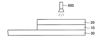
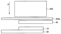
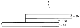
- connection method concerning embodiment of this invention It is sectional drawing which shows one process of the connection method concerning embodiment of this invention. It is sectional drawing which shows one process of the connection method concerning embodiment of this invention. It is sectional drawing which shows one process of the connection method concerning embodiment of this invention. It is sectional drawing which shows one process of the connection method concerning embodiment of this invention. 1 is a cross-sectional view illustrating a configuration of an anisotropic conductive connection structure according to an embodiment of the present invention.
- connection film 10 is a film that connects the first component and the second component.
- the first part and the second part may be arbitrary articles.
- both the first component and the second component may be electronic components, and may be other types of articles.
- an electronic component it may include an electrode or the like that is electrically conductive, and may be connected so as to be electrically conductive (for example, anisotropically connected via conductive particles).
- the first electronic component and the second electronic component may be opposed to each other.
- connection film 10 connects these electronic components (the first electronic component 30 and the second electronic component 40) via conductive particles.
- An anisotropic conductive film for anisotropic conductive connection may be used.
- An anisotropic conductive film is an example of a conductive connection film (a film capable of expressing conductivity).
- the connection film 10 is not limited to a conductive connection film such as an anisotropic conductive film, and may be, for example, a film containing no conductive particles.
- the connection film 10 does not include conductive particles, the first component and the second component may be electronic components or other types of components.
- the connection film 10 does not include conductive particles, and may electrically connect the first electronic component 30 and the second electronic component 40. Further, the connection film can be used without being used for electrical connection.
- connection film 10 is an anisotropic conductive film
- the curing of the thermosetting resin may be started at the time of temporary bonding, as described above. If a part of the thermosetting resin is cured at the time of temporary bonding, the thermosetting resin may not flow sufficiently at the time of final compression bonding. As a result, the conductive particles sandwiched between the electrode terminal of the first electronic component and the electrode terminal of the second electronic component are not sufficiently compressed, and a problem such as poor connection may occur. That is, not only the connection strength is reduced, but also a problem of poor connection may occur.
- the heating temperature at the time of temporary bonding is lower than the curing start temperature of the thermosetting resin, the progress of curing of the thermosetting resin at the time of temporary bonding can be suppressed (minimized).
- anisotropic conductive film anisotropic conductive connection or a method of manufacturing an anisotropic conductive connector
- the anisotropic conductive film is drawn out from the reel by a predetermined length and mounted on the first electronic component. Subsequently, the anisotropic conductive film is pressurized while being heated, so that the anisotropic conductive film is temporarily attached on the first electronic component. The above steps are repeated. In this line, there is a high possibility that the above-mentioned blurring or the like will occur. Thus, in order to use the connection film continuously and stably, the performance as in the present embodiment is required.
- the connection film 10 contains a film-forming resin and a curable resin.
- the connection film 10 may further include conductive particles.
- the film-forming resin gives the connection film 10 a film-forming property.
- the film-forming resin may be any resin as long as it can impart film-forming properties to the connection film 10.
- the film-forming resin may be an organic resin having an average molecular weight of 10,000 or more.
- the film-forming resin is preferably an organic resin having an average molecular weight of 10,000 or more and 80,000 or less from the viewpoint of improving applicability or film-forming property.
- various resins such as a phenoxy resin, a polyester urethane resin, a polyester resin, a polyurethane resin, and a modified resin thereof can be used.
- the film-forming resin is preferably a phenoxy resin from the viewpoint of improving film-forming properties and adhesion reliability.
- known additives such as rubber and elastomer may be appropriately compounded in the connection film 10.
- a curable resin is a resin that can be cured by either light irradiation or heating.
- the connection film 10 can be cured by either light irradiation or heating.
- the connection film 10 can be temporarily attached by light irradiation. In other words, there is no need to perform heating during the temporary bonding (or minimum heating is sufficient).
- the connection film 10 may be slightly cured by light irradiation, but there is no problem as long as the conductive particles can be sufficiently sandwiched or compressed at the time of the final pressure bonding. Even if the connection film does not contain conductive particles, there is no problem as long as it does not hinder the connection by the final pressure bonding.
- composition example of the curable resin is as follows.
- the following polymerizable compounds and various curing initiators are examples, and the invention is not limited thereto.
- composition example 1 the curable resin includes a polymerizable compound, a thermosetting initiator that starts curing of the polymerizable compound by heating, and a photocuring initiator that starts curing of the polymerizable compound by light irradiation.
- the photocuring initiator may be omitted. That is, the curable resin may have a composition including a polymerizable compound and a thermosetting initiator that starts curing of the polymerizable compound by heating.
- the polymerizable compound is a resin that can be cured by any of a thermosetting initiator and a photocuring initiator.
- the cured polymerizable compound adheres the first electronic component 30 and the second electronic component 40, and when the connection film 10 includes conductive particles, converts the conductive particles into an anisotropic conductive layer 10a ( The connection film 10 is cured (see FIG. 4). That is, although the details will be described later, some conductive particles are sandwiched between the first electrode terminal group and the second electrode terminal group in the anisotropic conductive layer 10a, and these electrode terminal groups are made conductive. .
- the cured polymerizable compound mainly maintains the state in which the conductive particles sandwiched between the terminal groups can maintain the state, and maintains the state in which the electronic components are bonded to each other as an adhesive.
- the polymerizable compound include an epoxy polymerizable compound and an acrylic polymerizable compound.
- the epoxy polymerizable compound is a monomer, oligomer, or prepolymer having one or more epoxy groups in one molecule.
- epoxy polymerizable compound examples include various bisphenol type epoxy resins (bisphenol A type, F type, etc.), polyglycidyl ether, polyglycidyl ester, novolak type epoxy resin, various modified epoxy resins such as rubber and urethane, and naphthalene type epoxy. Resin, biphenyl epoxy resin, phenol novolak epoxy resin, stilbene epoxy resin, triphenolmethane epoxy resin, dicyclopentadiene epoxy resin, triphenylmethane epoxy resin, glycidylamine epoxy compound, glycidyl ester epoxy compound And prepolymers thereof.
- bisphenol type epoxy resins bisphenol A type, F type, etc.
- polyglycidyl ether polyglycidyl ester
- novolak type epoxy resin various modified epoxy resins such as rubber and urethane
- naphthalene type epoxy examples include various modified epoxy resins such as rubber and urethane, and naphthalene type epoxy.
- Resin bipheny
- the acrylic polymerizable compound is a monomer, oligomer, or prepolymer having one or more acrylic groups in one molecule.
- examples of the acrylic polymerizable compound include methyl acrylate, ethyl acrylate, isopropyl acrylate, isobutyl acrylate, epoxy acrylate, ethylene glycol diacrylate, diethylene glycol diacrylate, trimethylolpropane triacrylate, dimethylol tricyclodecane diacrylate, and tetramethylene glycol.
- thermosetting initiator is a curing initiator that starts curing of the polymerizable compound by heating.
- thermal curing initiator examples include a thermal anionic or thermal cationic curing initiator for curing an epoxy polymerizable compound, and a thermal radical curing initiator for curing an acrylic polymerizable compound.
- an appropriate thermosetting initiator may be selected depending on the polymerizable compound.
- thermal anionic curing initiator examples include organic acid dihydrazide, dicyandiamide, amine compound, polyamidoamine compound, cyanate ester compound, phenolic resin, acid anhydride, carboxylic acid, tertiary amine compound, imidazole, Lewis acid, Examples include Bronsted acid salts, polymercaptan-based curing agents, urea resins, melamine resins, isocyanate compounds, and blocked isocyanate compounds. One or more of these may be used in any combination.
- thermal cationic curing initiator examples include iodonium salts, sulfonium salts, phosphonium salts, ferrocenes and the like. One or more of these may be used in any combination.
- thermal radical curing initiator examples include organic peroxides and azo compounds. One or more of these may be used in any combination.
- the photo-curing initiator is a curing initiator that starts curing of the polymerizable compound by light irradiation.
- the photocuring initiator include a photoanionic or cationic cationic curing initiator for curing an epoxy polymerizable compound, and a photoradical polymerization initiator for curing an acrylic polymerizable compound.
- an appropriate photocuring initiator may be selected depending on the polymerizable compound.
- Examples of the photoanionic curing initiator include acetophenone, O-aroyl oxime, and nifedipine which generate a base by light.
- photocationic curing initiator examples include onium salts such as iodonium salts, sulfonium salts, aromatic diazonium salts, phosphonium salts and selenonium salts, metal arene complexes, complex compounds such as silanol / aluminum complexes, benzoin tosylate, o- Nitrobenzyl tosylate and the like can be used.
- the counter anion when forming a salt include propylene carbonate, hexafluoroantimonate, hexafluorophosphate, tetrafluoroborate, and tetrakis (pentafluorophenyl) borate. One or more of these may be used in any combination.
- photo-radical curing initiators include benzoin ethers such as benzoin ethyl ether and isopropyl benzoin ether, benzyl ketals such as benzyl and hydroxycyclohexyl phenyl ketone, ketones such as benzophenone and acetophenone and derivatives thereof, thioxanthones and bisimidazoles And the like. One or more of these may be used in any combination.
- composition example 2 the curable resin contains a polymerizable compound and a thermo-light curing initiator that starts curing of the polymerizable compound by both heating and light irradiation.
- the polymerizable compound is the same as in Composition Example 1.
- the connection film may be made of a thermoplastic resin (including rubber and elastomer).
- modified thermoplastic resins include JP-A-2014-060025, JP-A-2015-170581, and JP-A-2015-147832).
- heat-light curing initiator examples include, among the curing initiators listed above, a thermal cationic curing initiator, a thermal anion, a radical polymerization initiator, and the like.
- the curable resin may further contain a photocuring initiator. Thereby, the hardening at the time of temporary bonding can be performed more reliably.
- curing of a polymerizable compound by irradiation of light with a photo-curing initiator or a thermo-light curing initiator is also referred to as “photo-curing”, and the heat-curing initiator or the thermo-photo-curing initiator is polymerized by heating. Curing the reactive compound is also referred to as “thermal curing”.
- the curable resin further contains a light absorber in addition to the composition of Composition Example 1 or Composition Example 2 described above.
- the light absorber slightly generates heat by light irradiation. Therefore, the light absorber generates heat by light irradiation at the time of temporary attachment.
- the connection film 10 is slightly melted by the heat generation, and is fixed to the first electronic component 30. Therefore, when the curable resin contains a light absorbing agent, the connection film 10 can be temporarily attached to the first electronic component 30 more firmly.
- the wavelength of light absorbed by the light absorber is not particularly limited, but may be, for example, about 230 to 500 nm.
- light absorbers examples include benzotriazole-based, triazine-based, and benzophenone-based ultraviolet absorbers.
- a photoradical curing initiator when using a photocationic curing initiator as a photocuring initiator, a photoradical curing initiator may be used as a light absorber.
- the curable resin may have any of composition examples 1 to 3, but composition example 3 is preferred.
- the conductive particles are formed in the anisotropic conductive layer 10a in the electrode terminal group on the first electronic component 30 (hereinafter, also referred to as "first electrode terminal group”. Generally, the electrode terminals are arranged). This is a material that conducts between the first electrode terminal group and the electrode terminal group on the second electronic component 40 (hereinafter, also referred to as a “second electrode terminal group”). Specifically, the conductive particles sandwiched between the first electrode terminal group and the second electrode terminal group in the anisotropic conductive layer 10a conduct these electrode terminal groups.
- the other conductive particles do not conduct between the terminals in the arrangement direction of the first electrode terminal group and the second electrode terminal group that sandwich the conductive particles (that is, the other conductive particles do not conduct in the arrangement direction of the electrode terminal group). Short circuit). Therefore, the conductive particles maintain the insulating property between the electrode terminals constituting the first electrode terminal group and between the electrode terminals constituting the second electrode terminal group in the anisotropic conductive layer 10a while maintaining the insulation property between the electrode terminals. And the second electrode terminal group can be conducted. That is, the conductive particles are interposed between the electrode terminals constituting the first electrode terminal group and the electrode terminals constituting the second electrode terminal group opposed thereto in the anisotropic conductive layer 10a.
- the conductive particles may be dispersed to such an extent that they do not cause a short circuit (they may be kneaded in the resin of the connection film 10), or may be arranged on the connection film 10 so as to be individually independent in a film plan view. . This arrangement is appropriately set according to the size of each electrode terminal, the distance in the arrangement direction of the electrode terminals, and the like, but may be regular.
- the connection film 10 is a film other than the conductive connection film (that is, when the connection film is not required to be conductive by the conductive particles), the conductive particles may not be included in the connection film 10. .
- connection films include WO2018 / 051799 and WO2018 / 074318.
- regular arrangement of the conductive particles in the anisotropic conductive film include JP-A-2016-066573 and JP-A-2016-103476.
- the structure of the conductive particles is not particularly limited, and may be so-called metal-coated resin particles or metal particles (for example, gold, silver, copper, nickel, palladium, solder, etc., and may be an alloy. ). Such conductive particles may be subjected to an insulation treatment to such an extent that the outermost surface does not hinder its conduction function. This is to prevent adverse effects due to continuous particles. Note that, in the case where the conductive particles are metal-coated resin particles, repulsion after compression of the resin particles makes it easier to obtain conduction between the first electrode terminal group and the second electrode terminal group, which is preferable in some cases.
- the resin particles constituting the core of the metal-coated resin particles are preferably particles made of a plastic material having excellent compression deformation.
- the material constituting the resin particles examples include a (meth) acrylate resin, a polystyrene resin, a styrene- (meth) acrylic copolymer resin, a urethane resin, an epoxy resin, a phenol resin, and an acrylonitrile styrene (AS) resin.
- the (meth) acrylic resin has a (meth) acrylic acid ester and, if necessary, a reactive double bond copolymerizable therewith.
- Two or more conductive particles may be used. In this case, for example, two or more kinds of different metal-coated resin particles may be used. Therefore, the combination of the conductive particles is not particularly limited.
- the coating layer that covers the resin particles is made of a conductive material.
- examples of the material constituting the coating layer include gold, silver, copper, nickel, palladium, and the like, and alloys thereof.
- the coating layer may be composed of one or more of these, or may be composed of two or more layers.
- connection film 10 may include various additives in addition to the above components.
- additives that can be added to the connection film 10 include a silane coupling agent, an inorganic filler, a coloring agent, an antioxidant, and a rust inhibitor.
- the type of the silane coupling agent is not particularly limited.
- examples of the silane coupling agent include epoxy-based, amino-based, mercapto sulfide-based, and ureide-based silane coupling agents.
- the inorganic filler is an additive for adjusting the fluidity and the film strength of the connection film 10.
- the type of the inorganic filler is not particularly limited. Examples of the inorganic filler include silica, talc, titanium oxide, calcium carbonate, and magnesium oxide.
- connection film 10 is not particularly limited. However, if the film is too thick, the amount of unnecessary resin becomes too large, and there is a problem in fluidity and the like. Therefore, it is preferably 200 ⁇ m or less, more preferably 100 ⁇ m or less, and even more preferably 40 ⁇ m or less. If it is too thin, it becomes difficult to handle, so it is preferably at least 5 ⁇ m, more preferably at least 12 ⁇ m. Further, the connection film 10 may have a long shape. The long connection film 10 may be cut into an appropriate length for use.
- the connection film 10 may have a single-layer structure or a multilayer structure. For example, the connection film 10 may have a two-layer structure, one layer may be an ACF layer (a layer containing conductive particles), and the other layer may be an NCF layer (a layer containing no conductive particles).
- a release film 20 is provided on one surface of the connection film 10. It is preferable that the peel strength (force required for peeling) between the release film 20 and the connection film 10 be reduced by light irradiation. Thereby, the release film 20 can be easily peeled off from the connection film 10 after the temporary attachment.
- the release film 20 is preferably a photocurable film that is cured by light irradiation.
- the release film 20 since the peel strength between the release film 20 and the connection film 10 is greatly reduced by light irradiation, the release film 20 can be more easily peeled off from the connection film 10 after the temporary attachment.
- An example of the photocurable film includes an ultraviolet (UV) cured film.
- the release film 20 may be of a type that foams by light irradiation.
- the peel strength between the release film 20 and the connection film 10 is greatly reduced by light irradiation, the same effect can be expected.
- Such a release film 20 may have optical transparency.
- other mechanisms are not particularly limited as long as the same effect (a decrease in the peel strength between the release film and the connection film due to light irradiation) is obtained and the performance of the connection film is not hindered.
- the connection film 10 may be slightly cured by light irradiation at the time of temporary attachment. Such curing also reduces the peel strength between the release film 20 and the connection film 10. Therefore, the release film 20 is not necessarily limited to a photocurable film, and for example, a release film used for a conventional anisotropic conductive film may be used.
- a release film used for a conventional anisotropic conductive film may be used as the release film 20, a film including PET (Poly Ethylene Terephthalate), OPP (Oriented Polypropylene), PMP (Poly-4-methylpentene-1), PTFE (Polytetrafluoroethylene), or the like may be used.
- a release agent such as silicone may be applied to the surface of a film made of these materials.
- the release film 20 may be considered to be integrated with the connection film 10 so as to be peelable, and to have rigidity and flexibility to the extent that it can be wound.
- connection structure a method for manufacturing the connection structure according to the present embodiment will be described with reference to FIGS.
- the method of manufacturing the connection structure will be described by taking the case where the connection film 10 is an anisotropic conductive film as an example, but it is needless to say that the connection film 10 may be another type of connection film.
- the temporary compression bonding of the connection film on the components and the final compression bonding of the components can be performed by the same steps as described below.
- the method for manufacturing a connection structure according to the present embodiment includes a connection film mounting step, a temporary bonding step, a peeling step, an electronic component mounting step, and a final pressure bonding step.
- each step will be described.
- connection film mounting step As shown in FIG. 1, the other surface of the connection film 10 (that is, the exposed surface on which the release film 20 is not provided) is in contact with the first electronic component 30. Is mounted on the first electronic component 30. Specifically, the connection film 10 is mounted on the region where the first electrode terminal group is formed.
- the first electronic component 30 may be any electronic component having the above-described first electrode terminal group.
- the first electronic component 30 may be a substrate on which a first electrode terminal group is formed (hereinafter, also referred to as a “first substrate”).
- the first electrode terminal group may be composed of ITO (indium tin oxide) or may be composed of a metal film. Examples of the metal constituting the metal film include gold, silver, copper, aluminum, zinc, titanium, and alloys of two or more of these.
- An insulating layer oxide film may be formed on the surface of the electrode terminal.
- the material forming the first substrate is an anisotropic conductive connection structure 1 (a structure in which the first electronic component 30 and the second electronic component 40 are anisotropically conductively connected; see FIG. 4). What is necessary is just to select according to the like.
- the first substrate may be formed of a transparent plastic substrate.
- the first substrate is made of, for example, polycarbonate, acrylic, polyethylene terephthalate (PET), triacetyl cellulose, cyclic olefin resin (COC), or the like.
- the first substrate may be made of a transparent glass or the like.
- connection film 10 is temporarily attached on the first electronic component 30.
- light is applied to the connection film 10 from a light source 600 installed on the back side of the first electronic component 30.
- the connection film 10 may be pressurized while irradiating the connection film 10 with light.
- pressure is applied, light irradiation may be performed before the pressure is applied.
- the position of the light source 600 is not limited to this, and may be above the release film 20 as shown in FIG. 2B. This is because even if light is irradiated from the release film 20 side, the performance is satisfied if the peel strength with the connection film 10 is reduced.
- pressure is applied in FIG.
- connection film 10 is temporarily attached to the first electronic component 30. By such temporary attachment, the connection film 10 is fixed (temporarily attached) to the first electronic component 30.
- the photo-curing initiator (or thermo-photo-curing initiator) in the curable resin slightly cures the polymerizable compound, but the connection film 10 is not substantially cured, or if cured, the degree of curing. Is slight.
- the connection film 10 in this connection method is an anisotropic conductive film as an example. Therefore, in order to evaluate whether or not temporary bonding has been performed as a property of the connection film, it is assumed that temporary bonding has been performed when the following conditions 1 and 2 are satisfied. This is because, in the case where the conductivity between the articles does not matter, if the conditions 1 and 2 are satisfied, the temporary bonding is practically no problem.
- Condition 3 may be applied when the connection film 10 is a conductive connection film such as an anisotropic conductive film or when electronic components are connected to each other without containing conductive particles. This is because, in the present embodiment, the condition 3 is used in order to check whether the reaction is excessively progressing during the temporary attachment.
- the connection film 10 is a conductive connection film such as an anisotropic conductive film, or when electronic components are electrically connected to each other without containing conductive particles
- the connection between the conductive particles or terminals in the film is performed. Since the performance is obtained by obtaining continuity between the connected objects by the direct connection, the evaluation can be performed under more precise conditions by adding the condition 3.
- Condition 3 below is an example of the COG connection of the anisotropic conductive connection. It should be noted that since the required performance (conduction resistance) differs depending on the combination of the connection components, the desired conduction resistance value after the acceleration test may be changed if the combination of the connection components changes.
- connection film 10 is a conductive connection film such as an anisotropic conductive film as a condition of the temporary bonding
- the pressure (MPa) and the integrated irradiation amount per unit area may be adjusted so as to satisfy the above conditions 1 to 3.
- the pressure may be 0.5 MPa or more and 2 MPa or less
- the integrated irradiation amount per unit area may be 150 to 500 (mW ⁇ sec / cm 2 ).
- the integrated irradiation amount per unit area is preferably from 200 to 400 (mW ⁇ sec / cm 2 ), and more preferably from 250 to 300 (mW ⁇ sec / cm 2 ). When the integrated irradiation amount is insufficient, light irradiation may be performed again. On the other hand, it is preferable that the integrated irradiation amount per unit area is as small as possible within a range where the conditions 1 to 3 are satisfied. This is for the purpose of increasing the fluidity of the connection film 10 at the time of final pressure bonding as much as possible.
- the release film 20 is made of the above-described photocurable film (or when a light irradiation film is laminated on the release film 20), it is possible to perform temporary bonding that satisfies the above conditions 1 to 3 with a smaller integrated irradiation amount. it can.
- the connecting film 10 contains a light absorbing agent, the resin portion of the connecting film 10 is melted by the heat generated by the light absorbing agent and adheres to the first electronic component 30. 10 can be firmly temporarily attached to the first electronic component 30.
- the pressing force and the integrated irradiation amount may be adjusted in the same manner as described above so that the conditions 1 and 2 are satisfied. This is not limited to the above, and may be appropriately adjusted according to the purpose.
- thermosetting start temperature of the curable resin ie, the thermosetting initiator
- the temporary bonding can be performed with little or no thermosetting of the thermosetting initiator or the thermosetting initiator.
- the temperature of the connection film 10 at the time of temporary bonding did not exceed the range of normal temperature (here, about 25 ° C. ⁇ 15 ° C.). .
- the thermosetting start temperature is higher than normal temperature.
- the thermosetting start temperature of the curable resin even when the thermosetting start temperature of the curable resin is low, it is possible to perform the temporary bonding without substantially performing the thermosetting on the thermosetting initiator or the thermolight curing initiator. . Therefore, for example, in a clean environment where room temperature can be maintained, other conditions are less likely to be restricted. For example, in a region where the temperature is high, it is less likely to be limited by the provisional attachment and the accompanying production of the connection body. I think this is an advantage for industrial promotion.
- connection film 10 is not substantially cured or slightly cured by light irradiation (that is, light cured). Even when the connection film 10 is slightly cured, the conduction resistance after the final pressure bonding is a good value as shown in the examples described later. That is, even when the connection film 10 is not substantially cured by light irradiation or is slightly cured, the fluidity of the connection film 10 at the time of the final pressure bonding is sufficiently ensured. Therefore, the conductive particles disposed between the electrode terminal of the first electronic component 30 and the electrode terminal of the second electronic component 40 are sandwiched by these electrode terminals during the final compression bonding.
- the temporary bonding is performed by light irradiation. Therefore, even if the connection film 10 is a conductive connection film such as the anisotropic conductive film 10 or connects electronic components without containing conductive particles, even when the thermosetting start temperature is low, Temporary bonding satisfying the above conditions 1 to 3 can be performed. When the conductivity between the articles does not matter, even when the thermosetting start temperature is low, the temporary bonding satisfying the above conditions 1 and 2 can be performed.
- connection film 10 is temporarily attached on the first electronic component 30, the connection film 10 is held on the first electronic component 30.
- the second electronic component 40 is mounted on the connection film 10. Specifically, the second electronic component 40 is mounted on the connection film 10 such that the region where the second electrode terminal group is formed contacts the connection film 10.
- the second electronic component 40 may be any electronic component having the above-described second electrode terminal group.
- the second electronic component 40 may be a substrate on which a second electrode terminal group is formed (hereinafter, also referred to as a “second substrate”).
- the material of the second electrode terminal group may be the same as that of the first electrode terminal group.
- the type of the second substrate is not particularly limited, and may be the same as the first substrate.
- the second substrate may be a so-called flexible substrate, or may be an integrated circuit (IC chip). Note that the first electronic components 30 or the second electronic components 40 may be connected to each other (for example, an integrated circuit may be stacked).
- the second electronic component 40 is fully pressure-bonded to the connection film 10.
- the cushioning member 200 a is installed on the second electronic component 40.
- the main crimping tool head 300 is moved in the direction of the arrow A (that is, downward), and the main crimping tool head 300 set at a predetermined temperature (heated) in advance is pressed against the cushioning material 200a.
- the second electronic component 40 is pressed.
- the pressurization is released. That is, the second electronic component 40 is pressed while the connection film 10 is heated. As a result, the second electronic component 40 is fully pressure-bonded to the first electronic component 30.
- the anisotropic conductive connection structure 1 is a structure in which a first electronic component 30 and a second electronic component 40 are anisotropically conductively connected by an anisotropic conductive layer 10a.
- the anisotropic conductive layer 10a is obtained by curing the connection film 10.
- the conductive resistance after the final pressure bonding can be reduced while the temporary bonding is performed accurately, so that a highly reliable anisotropic conductive connection structure 1 can be manufactured with high productivity.
- the connection film 10 is another type of connection film, the temporary bonding can be performed accurately.
- anisotropic conductive films according to Experimental Examples 1-1 to 3-5 were produced in the following steps. That is, phenoxy resin YP-70 (manufactured by Nippon Steel & Sumikin Chemical Co., Ltd.), liquid epoxy resin EP828 (manufactured by Mitsubishi Chemical Corporation), solid epoxy resin YD014 (manufactured by Nippon Steel & Sumikin Chemical Co., Ltd.), and conductive particles Certain AUL704 (manufactured by Sekisui Chemical Co., Ltd.), SI-80L and SI-60L (both manufactured by Sanshin Chemical Co., Ltd.), which are thermal cation curing initiators, and LA-31 (manufactured by ADEKA), which is a light absorber, are listed in the table.
- a coating liquid for the ACF layer was prepared.
- the phenoxy resin is an example of a film-forming resin
- the liquid epoxy resin and the solid epoxy resin are examples of a polymerizable compound.
- the thermal cationic curing initiator is an example of a thermo-light curing initiator.
- a coating liquid for the NCF layer was prepared by removing the conductive particles from the coating liquid for the ACF layer.
- release films a PET film (Purex, manufactured by Teijin Limited, 50 ⁇ m in thickness) and a UV-curable film (SELFA-SE, manufactured by Sekisui Chemical Co., Ltd., 50 ⁇ m in thickness) were prepared.
- the PET film is described as “normal substrate”, and the UV cured film is described as “UV release substrate”.
- the coating liquid for the NCF layer was applied on a release film (PET film or UV cured film) so as to have a thickness of 10 ⁇ m after drying, and dried in an oven.
- a release film PET film or UV cured film
- an NCF layer was formed on the release film.
- a coating liquid for an ACF layer was applied on a PET film so as to have a thickness of 10 ⁇ m after drying, and dried in an oven.
- the ACF layer was laminated on the NCF layer. That is, each layer is laminated in the order of PET film or UV cured film / NCF layer / ACF layer.
- connection films according to Experimental Examples 1-1 to 3-5 have a two-layer structure of the NCF layer and the ACF layer. Further, the above components were mixed with the compositions shown in Table 4 to prepare a coating liquid for the NCF layer. Then, a coating liquid for the NCF layer was applied on the release film so as to have a thickness of 20 ⁇ m after drying, and dried in an oven. Through the above steps, connection films according to Experimental Examples 4-1 to 4-3 were obtained. Therefore, the connection films according to Experimental Examples 4-1 to 4-3 have a single-layer structure of the NCF layer. Tables 1 to 4 show the composition of the connection film and the type of the release film. The connecting film was cut out to a width of 4.0 mm and a length of 25.0 mm for use.
- an ITO patterned glass having a thickness of 0.5 mm was prepared.
- a first electrode terminal group made of ITO is formed on the ITO pattern glass so as to face the second electrode terminal group of the second electronic component.
- the second electronic component is an evaluation IC having a thickness of 0.5 mm and an outer shape of 1.8 mm ⁇ 20 mm, and a bump of 25 ⁇ m ⁇ 25 ⁇ m has a distance between bumps of 25 ⁇ m and 300 mm on one side on the long side of the evaluation IC. It is formed in an array.
- the second electrode terminal group (bump of the evaluation IC) is an Au plating bump (height: 15 ⁇ m). Further, a polyimide film and a glass plate were prepared (details will be described later).
- connection film was temporarily attached on the first electronic component by the connection method described above. Specifically, first, a connection film was mounted on the first electronic component. Here, the connection film was mounted on the region where the first electrode terminal group was formed.
- connection film was temporarily attached on the first electronic component. Specifically, the connection film was pressed.
- the size of the crimping surface of the temporary bonding tool head was 10.0 mm in width and 40.0 mm in length.
- the pressurization was basically performed at room temperature (RT), but was performed by heating in some experimental examples. The pressurization and heating were performed under the conditions of buffer material: silicon rubber (thickness: 350 ⁇ m) and temporary bonding conditions (pressure conditions during temporary bonding): 70 ° C.-1 MPa-1 second. Tables 1 to 3 show the pressurizing conditions (heating temperature-pressing force-pressing time) at the time of temporary bonding.
- connection film was pressed while irradiating the connection film with light. Thereby, the connection film was temporarily attached to the first electronic component.
- SP-9 manufactured by Ushio Inc. was used as a light source.
- the position of the light source was on the back side of the first electronic component as shown in FIG. 2A.
- the wavelength of the light emitted from this light source was 365 nm, and the irradiation area (the area where the light on the connection film hit) was about 4.0 mm in width and about 44.0 mm in length.
- the irradiation intensity and irradiation time per unit area were different values for each experimental example.
- the irradiation intensity was set to 300 mW / cm 2 and the irradiation time was set to 1 sec. Pressurization and light irradiation were started simultaneously.
- the temperature of the connection film was measured by installing a thermocouple at a location where the connection film was provided and measuring the temperature profile when performing temporary bonding. Also in the example, the temperature of the connection film was equal to or lower than the upper limit of normal temperature (about 40 ° C.). Therefore, it is presumed that heat hardening hardly occurred.
- the first electronic component and the second electronic component were fully press-bonded by the connection method described above. Specifically, the second electronic component was mounted on the connection film such that the region where the second electrode terminal group was formed was in contact with the connection film. Next, the cushioning material was set on the second electronic component. Next, the tooling tool head was moved in the direction of arrow A shown in FIG. 3 (that is, downward), and the tooling tool tool that had been set (heated) at a predetermined temperature in advance was pressed against the cushioning material. Thereby, the second electronic component was pressurized. After a lapse of a predetermined time, the pressurization was released. That is, the second electronic component was pressed while heating the connection film.
- the cushioning material was the same as the cushioning material at the time of temporary attachment.
- the tool head for final crimping was the same as the tool head for temporary bonding.
- Tables 1 to 3 summarize the main bonding conditions (heating temperature-pressure-pressure-pressure time) of the connection film. Thus, an anisotropic conductive connection structure was obtained.
- the following reliability evaluation test was performed to evaluate the reliability of the obtained anisotropic conductive connection structure. Specifically, the conduction resistance of the anisotropic conductive connection structure was measured. The conduction resistance was measured by a four-terminal method using a digital multimeter (product number: Digital Multimeter 7555, manufactured by Yokogawa Electric Corporation), and the conduction resistance (initial conduction resistance) when a current of 1 mA was passed was measured. . The initial conduction resistance was A (pass) when the resistance was 2 ⁇ or less, and B (fail) when the resistance exceeded 2 ⁇ . Next, the anisotropic conductive connection structure was kept in an environment of a temperature of 85 ° C.
- Second Temporary Pasting Test a test similar to the above-described first temporary bonding test was performed in which the first electronic component was replaced with a polyimide film (Toray DuPont, product name: Kapton, dimensions: 4 cm ⁇ 3 cm) having a thickness of 50 ⁇ m. Was done. Table 4 shows the pressing conditions (heating temperature-pressing force-pressing time) at the time of temporary bonding.
- connection strength test> First, the above-mentioned main compression was performed by replacing the second electronic component with a glass plate having a thickness of 0.5 mm. Table 4 summarizes the conditions for the final pressure bonding (heating temperature-pressure-pressure-pressure time). Thus, a connection structure was obtained. Next, the peel strength of the connection structure was measured. The peel strength was measured using a tensile tester (trade name: Tensilon, manufactured by A & D Corporation). Specifically, a polyimide film is cut into a width of 1 cm, a glass plate is placed and fixed horizontally, and then, when the polyimide film is pulled at an angle of 90 degrees, the tensile strength (peel strength) at which the polyimide film peels off is obtained. Was measured. When the connection strength was 7N or more, A was set, when the connection strength was 2N or more and less than 7N, B was set, and when the connection strength was less than 2N, C was set. A is a pass level.
- the release film is a “UV release substrate”.
- the temporary bonding test result was rejected. It is presumed that the accumulated irradiation amount was insufficient. However, when the integrated irradiation amount was further increased as in Experimental Example 2-2, a passable temporary bonding test result was obtained. In the case of Experimental Example 2-3, the result of the temporary bonding test was also passed. Note that the integrated irradiation amount of Experimental Example 2-2 is lower than that of Experimental Example 1-3. Since the release film is a “UV release substrate”, it is presumed that the release film could be peeled from the connection film even with a small integrated irradiation amount (that is, even when the adhesive strength of the connection film was small).
- connection strength was examined.
- the connection strength after the final pressure bonding was rejected. Since the temporary bonding test was performed by heating, it is presumed that the curing of the thermosetting resin progressed during the temporary bonding test, and sufficient connection strength was not obtained after the final pressure bonding.
- a temporary bonding test was performed by light irradiation.
- the connection strength after the final crimping was acceptable, and in Experimental Example 4-2, the temporary bonding test failed.
- connection strength test was not performed, the light was further irradiated in the temporary bonding test of Experimental Example 4-2, and a passable temporary bonding test result was obtained.
- an auxiliary agent such as a light absorber.
Landscapes
- Chemical & Material Sciences (AREA)
- Organic Chemistry (AREA)
- Engineering & Computer Science (AREA)
- Manufacturing & Machinery (AREA)
- Microelectronics & Electronic Packaging (AREA)
- Inorganic Chemistry (AREA)
- Adhesive Tapes (AREA)
- Adhesives Or Adhesive Processes (AREA)
- Wire Bonding (AREA)
- Electric Connection Of Electric Components To Printed Circuits (AREA)
Abstract
加熱を行わずに仮貼りを行うことが可能な、新規かつ改良された接続構造体の製造方法および接続フィルムを提供する。 上記課題を解決するために、本発明のある観点によれば、接続フィルムを用いて第1の部品と第2の部品とを接続する接続構造体の製造方法であって、接続フィルムの一方の面には剥離フィルムが設けられ、接続フィルムの他方の面が第1の部品に接触するように接続フィルムを第1の部品上に搭載する工程と、接続フィルムに光を照射することで、接続フィルムを第1の部品に仮貼りする工程と、剥離フィルムを接続フィルムから剥離する工程と、接続フィルム上に第2の部品を搭載する工程と、接続フィルムを加熱しながら第2の部品を加圧することで、第1の部品と第2の部品とを本圧着する工程と、を含む。
Description
本発明は、接続構造体の製造方法および接続フィルムに関する。本出願は、日本国において2018年9月7日に出願された日本特許出願番号特願2018-168304を基礎として優先権を主張するものであり、この出願は参照されることにより、本出願に援用される。
部品間に接続フィルムを挟持し、部品同士を加圧、加熱することで部品同士を接続することは様々な技術分野で広く行われている。接続フィルムは、熱硬化性樹脂を含み、加熱によって硬化する。このような技術の一例として、特許文献1~3に開示されるように、複数の電子部品同士を樹脂に含まれる導電性粒子を介して異方性導電接続する技術が知られている。この技術では、まず、第1の電子部品上に異方性導電フィルムを搭載する。ついで、異方性導電フィルムを加熱しながら加圧することで、第1の電子部品上に異方性導電フィルムを仮貼りする。ここで、異方性導電フィルムは、膜形成樹脂、熱硬化性樹脂、および導電性粒子を含む。
ついで、異方性導電フィルム上に第2の電子部品を搭載する。ついで、異方性導電フィルムを加熱しながら第2の部品を加圧することで、第1の電子部品と第2の電子部品とを本圧着する。この工程では、加圧および加熱によって異方性導電フィルムの樹脂成分が流動する一方で、第1の電子部品の電極端子と第2の電子部品の電極端子との間に配置された異方性導電フィルム内の導電性粒子が、これらの電極端子によって挟持される。さらに、上記加熱によって熱硬化性樹脂が硬化する(加熱によって樹脂流動が促進され、同時に硬化反応が行われる)。これにより、第1の電子部品と第2の電子部品とを異方性導電接続する。すなわち、異方性導電接続構造体を作製する。
上記のような仮貼り、本圧着の工程は異方性導電フィルムに限られず、様々な接続フィルムの分野で行われる。ところで、近年では、各部品に対する熱応力、熱負荷の影響を低減する等の観点から、異方性導電フィルムに限らず、様々な接続フィルムの分野において、本圧着時の加熱温度を低くしたいという要望が非常に強くなってきている。
本圧着時の加熱温度を低くするためには、熱硬化性樹脂の硬化開始温度を低くする必要がある。したがって、仮貼り時の加熱温度も必然的に低くする必要がある。仮貼り時の加熱温度が高いと仮貼り時に熱硬化性樹脂の硬化が開始されてしまう可能性があるからである。仮貼り時に熱硬化性樹脂の一部が硬化してしまう(硬化が進行してしまう)と、本圧着後に接続フィルムが十分な接続強度を発揮できない可能性がある。
仮貼り時の加熱温度を熱硬化性樹脂の硬化開始温度よりも低くすれば、仮貼り時における熱硬化性樹脂の硬化を抑制することができる。しかし、仮貼り温度が低すぎると、接続フィルムが接続対象の部品への貼着不良など不具合が生じる虞がある。また、仮貼り時の加熱温度を比較的低温で一定にすることは容易でない。これは、連続して接続を行う場合に、特に顕著である。これは、接続を繰り返すことでツールの温度が一定に保たれ難いからであり、温度が上ブレすれば仮貼りで接続フィルムに熱を過剰に与えることになり、また下ブレすれば接続対象の部品に貼着されない、といった仮貼り不良が懸念される。このように接着温度の硬化条件のマージンが小さい中でも、使用方法に不具合を生じさせないことは、大量生産や精密な生産条件を得る上で、強く求められる。接続フィルム自体の性能が高まると、この要請はより高まると予想される。
そこで、本発明は、上記問題に鑑みてなされたものであり、本発明の目的とするところは、比較的低温(例えば常温(=25℃±15℃)もしくは加熱を行わずに仮貼りを行うことが可能な、新規かつ改良された接続構造体の製造方法および接続フィルムを提供することにある。
上記課題を解決するために、本発明のある観点によれば、接続フィルムを用いて第1の部品と第2の部品とを接続する接続構造体の製造方法であって、接続フィルムの一方の面には剥離フィルムが設けられ、接続フィルムの他方の面が第1の部品に接触するように接続フィルムを第1の部品上に搭載する工程と、接続フィルムに光を照射することで、接続フィルムを第1の部品に仮貼りする工程と、剥離フィルムを接続フィルムから剥離する工程と、接続フィルム上に第2の部品を搭載する工程と、接続フィルムを加熱しながら第2の部品を加圧することで、第1の部品と第2の部品とを本圧着する工程と、を含むことを特徴とする、接続構造体の製造方法が提供される。
ここで、接続フィルムは、加熱及び光照射のいずれかによって硬化可能な樹脂であるか、または熱可塑性樹脂で構成されてもよい。
また、接続フィルムは、重合性化合物と、加熱により重合性化合物の硬化を開始させる熱硬化開始剤と、光照射により重合性化合物の硬化を開始させる光硬化開始剤とを含んでいてもよい。
また、接続フィルムは、重合性化合物と、加熱および光照射のいずれによっても重合性化合物の硬化を開始させる熱光硬化開始剤とを含んでいてもよい。
また、接続フィルムは、光照射により重合性化合物の硬化を開始させる光硬化開始剤をさらに含んでいてもよい。
また、接続フィルムは、光照射によって発熱する光吸収剤を含んでいてもよい。
また、剥離フィルムと接続フィルムとの剥離強度は、光照射によって低下してもよい。
また、第1の部品および第2の部品は電子部品であり、接続フィルムは、導電性粒子を含んでいてもよい。この導電性粒子によって、第1の部品と第2の部品とを異方性導電接続してもよい。また、接続フィルムは、導電性粒子を含まず、第1の部品と第2の部品とを電気的に接続してもよい。また、電気的な接続の用途でなくとも接続フィルムは使用できる。
本発明の他の観点によれば、第1の部品と第2の部品とを接続するための接続フィルムであって、接続フィルムは、剥離フィルム上に形成され、剥離フィルムと接続フィルムとの剥離強度は、光照射によって低下することを特徴とする、接続フィルムが提供される。
ここで、接続フィルムは、加熱及び光照射のいずれかによって硬化可能な樹脂であるか、または熱可塑性樹脂で構成されてもよい。
また、接続フィルムは、重合性化合物と、加熱により重合性化合物の硬化を開始させる熱硬化開始剤と、光照射により重合性化合物の硬化を開始させる光硬化開始剤とを含んでいてもよい。
また、接続フィルムは、重合性化合物と、加熱および光照射のいずれによっても重合性化合物の硬化を開始させる熱光硬化開始剤とを含んでいてもよい。
また、接続フィルムは、光照射により重合性化合物の硬化を開始させる光硬化開始剤をさらに含んでいてもよい。
また、接続フィルムは、光照射によって発熱する光吸収剤を含んでいてもよい。
また、第1の部品および第2の部品は電子部品であり、接続フィルムは、導電性粒子を含んでいてもよい。この導電性粒子によって、第1の部品と第2の部品とを異方性導電接続してもよい。また、接続フィルムは、導電性粒子を含まず、第1の部品と第2の部品とを電気的に接続してもよい。また、電気的な接続の用途でなくとも接続フィルムは使用できる。
以上説明したように本発明によれば、光照射により仮貼りを行うので、比較的低温(例えば常温(=25℃±15℃)もしくは加熱せずに仮貼りを行うことが可能となる。
以下に添付図面を参照しながら、本発明の好適な実施の形態について詳細に説明する。なお、本明細書及び図面において、実質的に同一の機能構成を有する構成要素については、同一の符号を付することにより重複説明を省略する。
<1.接続フィルムの構成>
まず、図1~図4に基づいて、本実施形態に係る接続フィルム10の構成について説明する。接続フィルム10は、第1の部品と第2の部品とを接続するフィルムである。第1の部品、第2の部品は任意の物品でよい。例えば、第1の部品及び第2の部品はいずれも電子部品であってもよく、他の種類の物品であってもよい。電子部品である場合、電気的に導通される電極等を備えていてもよく、これらが電気的に導通するように接続(例えば導電性粒子を介して異方性接続)されるように、第1の電子部品と第2の電子部品で対向して存在していてもよい。第1の物品及び第2の部品がいずれも電子部品となる場合、接続フィルム10は、これらの電子部品(第1の電子部品30、第2の電子部品40)を、導電性粒子を介して異方性導電接続する異方性導電フィルムであってもよい。以下、接続フィルム10が異方性導電フィルムである場合を一例として本実施形態を説明する。異方性導電フィルムは、導電性接続フィルム(導電性を発現可能なフィルム)の一例である。もちろん、接続フィルム10は異方性導電フィルム等の導電性接続フィルムに限られず、例えば導電性粒子を含まないフィルムであってもよい。接続フィルム10が導電性粒子を含まない場合であっても、第1の部品及び第2の部品は電子部品であってもよく、他の種類の部品であってもよい。例えば、接続フィルム10は、導電性粒子を含まず、第1の電子部品30と第2の電子部品40とを電気的に接続してもよい。また、電気的な接続の用途でなくとも接続フィルムは使用できる。
まず、図1~図4に基づいて、本実施形態に係る接続フィルム10の構成について説明する。接続フィルム10は、第1の部品と第2の部品とを接続するフィルムである。第1の部品、第2の部品は任意の物品でよい。例えば、第1の部品及び第2の部品はいずれも電子部品であってもよく、他の種類の物品であってもよい。電子部品である場合、電気的に導通される電極等を備えていてもよく、これらが電気的に導通するように接続(例えば導電性粒子を介して異方性接続)されるように、第1の電子部品と第2の電子部品で対向して存在していてもよい。第1の物品及び第2の部品がいずれも電子部品となる場合、接続フィルム10は、これらの電子部品(第1の電子部品30、第2の電子部品40)を、導電性粒子を介して異方性導電接続する異方性導電フィルムであってもよい。以下、接続フィルム10が異方性導電フィルムである場合を一例として本実施形態を説明する。異方性導電フィルムは、導電性接続フィルム(導電性を発現可能なフィルム)の一例である。もちろん、接続フィルム10は異方性導電フィルム等の導電性接続フィルムに限られず、例えば導電性粒子を含まないフィルムであってもよい。接続フィルム10が導電性粒子を含まない場合であっても、第1の部品及び第2の部品は電子部品であってもよく、他の種類の部品であってもよい。例えば、接続フィルム10は、導電性粒子を含まず、第1の電子部品30と第2の電子部品40とを電気的に接続してもよい。また、電気的な接続の用途でなくとも接続フィルムは使用できる。
ここで、接続フィルム10が異方性導電フィルムとなる場合を例に説明すると、上記の問題に加え、さらに以下の問題も考慮する必要がある。すなわち、仮貼り時の加熱温度が高いと、上述したように、仮貼り時に熱硬化性樹脂の硬化が開始されてしまう可能性がある。仮貼り時に熱硬化性樹脂の一部が硬化してしまうと、本圧着時に熱硬化性樹脂が十分に流動しなくなる可能性がある。この結果、第1の電子部品の電極端子と第2の電子部品の電極端子に挟持される導電性粒子は十分に圧縮されず、接続不良等の問題が生じうる。つまり、接続強度が低下するのみならず、接続不良の問題も生じうる。
仮貼り時の加熱温度を熱硬化性樹脂の硬化開始温度よりも低くすれば、仮貼り時における熱硬化性樹脂の硬化の進行を抑制する(最小限にする)ことができる。しかし、仮貼り工程を連続して行うといった製造ラインでは、加熱温度(加熱押圧するツールの温度)を一定にすることが容易でない。例えば、異方性導電フィルムを使用する(異方性導電接続、あるいは異方性導電接続体の製造方法)分野では、連続生産における製造ラインにおいて仮貼りを連続して行うことが一般的である。ここで、仮貼り工程を連続して繰り返し行う上記製造ラインでは、リールから異方性導電フィルムを所定長さ引き出して、第1の電子部品上に搭載する。ついで、異方性導電フィルムを加熱しながら加圧することで、第1の電子部品上に異方性導電フィルムを仮貼りする。以上の工程を繰り返し行う。このラインでは、上述した上ブレ等が生じる可能性が高い。このように、接続フィルムを連続的に且つ安定して使用する上では、本実施形態のような性能が求められることになる。
接続フィルム10は、膜形成樹脂と、硬化性樹脂とを含む。接続フィルム10は、導電性粒子を更に含んでもよい。膜形成樹脂は、接続フィルム10に成膜性を付与する。膜形成樹脂は、接続フィルム10に成膜性を付与できる樹脂であればどのようなものであってもよい。例えば、膜形成樹脂は、10000以上の平均分子量を有する有機樹脂であってもよい。膜形成樹脂は、塗布性又はフィルム形成性等を向上させる観点からは、10000以上80000以下の平均分子量を有する有機樹脂であることが好ましい。膜形成樹脂としては、例えば、フェノキシ樹脂、ポリエステルウレタン樹脂、ポリエステル樹脂、ポリウレタン樹脂、及びこれらの変性樹脂などの種々の樹脂を用いることができる。また、本実施形態では、これらの膜形成樹脂のうちいずれか1種だけを使用することもできるし、2種以上を任意に組み合わせて使用することもできる。なお、膜形成樹脂は、膜形成性および接着信頼性を良好にするという観点からは、フェノキシ樹脂であることが好ましい。また、接続フィルム10には、ゴムやエラストマーなどの公知の添加剤を適宜配合してもよい。
硬化性樹脂は、光照射及び加熱のいずれかによって硬化可能な樹脂である。これにより、接続フィルム10は、光照射及び加熱のいずれかによって硬化可能となっている。詳細は後述するが、接続フィルム10がこのような特徴を有するので、光照射によって接続フィルム10の仮貼りを行うことができる。つまり、仮貼り時に加熱を行う必要がない(もしくは最低限の加熱でよくなる)。さらに、光照射によって接続フィルム10がわずかに硬化する場合があるが、本圧着時に導電性粒子を十分に挟持もしくは圧縮することができれば問題はない。導電性粒子が含有されない接続フィルムであっても、本圧着による接続に支障をきたさない程度であれば問題はない。そのため、光照射による接続フィルムへの影響は無視できる程度のものであるか、そのように調整すればよく、接続不良等の問題は生じにくいと考えて差し支えない。硬化性樹脂の組成例は以下のとおりである。以下の重合性化合物や各種硬化開始剤は一例であり、これに限定されるものではない。
(組成例1)
組成例1では、硬化性樹脂は、重合性化合物と、加熱により重合性化合物の硬化を開始させる熱硬化開始剤と、光照射により重合性化合物の硬化を開始させる光硬化開始剤とを含む。なお、組成例1において、光硬化開始剤は省略されてもよい。すなわち、硬化性樹脂は、重合性化合物と、加熱により重合性化合物の硬化を開始させる熱硬化開始剤と、を含む組成であってもよい。
組成例1では、硬化性樹脂は、重合性化合物と、加熱により重合性化合物の硬化を開始させる熱硬化開始剤と、光照射により重合性化合物の硬化を開始させる光硬化開始剤とを含む。なお、組成例1において、光硬化開始剤は省略されてもよい。すなわち、硬化性樹脂は、重合性化合物と、加熱により重合性化合物の硬化を開始させる熱硬化開始剤と、を含む組成であってもよい。
重合性化合物は、熱硬化開始剤および光硬化開始剤のいずれによっても硬化可能な樹脂である。硬化した重合性化合物は、第1の電子部品30と第2の電子部品40とを接着するとともに、接続フィルム10が導電性粒子を含む場合には、導電性粒子を異方性導電層10a(接続フィルム10が硬化したもの。図4参照)内に保持する。すなわち、詳細は後述するが、一部の導電性粒子は、異方性導電層10a内で第1の電極端子群と第2の電極端子群とで挟持され、これらの電極端子群を導通させる。一方、その他の導電性粒子は、導電性粒子を挟持している第1の電極端子群及び第2の電極端子群の配列方向において端子間で導通させないようにあればよい。硬化した重合性化合物は、主に端子群で挟持された導電性粒子がその状態を維持できるように、また接着剤として電子部品同士が接着された状態を保持する。重合性化合物としては、例えばエポキシ重合性化合物、及びアクリル重合性化合物等が挙げられる。エポキシ重合性化合物は、1分子内に1つまたは2つ以上のエポキシ基を有するモノマー、オリゴマー、またはプレポリマーである。エポキシ重合性化合物としては、例えば、各種ビスフェノール型エポキシ樹脂(ビスフェノールA型、F型等)、ポリグリシジルエーテル、ポリグリシジルエステル、ノボラック型エポキシ樹脂、ゴムおよびウレタン等の各種変性エポキシ樹脂、ナフタレン型エポキシ樹脂、ビフェニル型エポキシ樹脂、フェノールノボラック型エポキシ樹脂、スチルベン型エポキシ樹脂、トリフェノールメタン型エポキシ樹脂、ジシクロペンタジエン型エポキシ樹脂、トリフェニルメタン型エポキシ樹脂、グリシジルアミン系エポキシ化合物、グリシジルエステル系エポキシ化合物、及びこれらのプレポリマー等が挙げられる。
アクリル重合性化合物は、1分子内に1つまたは2つ以上のアクリル基を有するモノマー、オリゴマー、またはプレポリマーである。アクリル重合性化合物としては、例えば、メチルアクリレート、エチルアクリレート、イソプロピルアクリレート、イソブチルアクリレート、エポキシアクリレート、エチレングリコールジアクリレート、ジエチレングリコールジアクリレート、トリメチロールプロパントリアクリレート、ジメチロールトリシクロデカンジアクリレート、テトラメチレングリコールテトラアクリレート、2-ヒドロキシ-1,3-ジアクリロキシプロパン、2,2-ビス[4-(アクリロキシメトキシ)フェニル]プロパン、2,2-ビス[4-(アクリロキシエトキシ)フェニル]プロパン、ジシクロペンテニルアクリレート、トリシクロデカニルアクリレート、トリス(アクリロキシエチル)イソシアネレート、ポリエーテルアクリレート、ポリエステルアクリレート、ポリエチレングリコールジアクリレート、ポリアルキレングリコールジアクリレート、ペンタエリスリトールアクリレート、2-シアノエチルアクリレート、シクロヘキシルアクリレート、ジシクロベンテニロキシエチルアクリレート、2-(2-エトキシエトキシ)エチルアクリレート、2-エトキシエチルアクリレート、2-エチルヘキシルアクリレート、n-ヘキシルアクリレート、2-ヒドロキシエチルアクリレート、ヒドロキシプロピルアクリレート、イソボルニルアクリレート、イソデシルアクリレート、イソオクチルアクリレート、n-ラウリルアクリレート、2-メトキシエチルアクリレート、2-フェノキシエチルアクリレート、テトラヒドロフルフリールアクリレート、ネオペンチルグリコールジアクリレート、ジペンタエリスリトールヘキサアクリレート、およびウレタンアクリレート等が挙げられる。本実施形態では、上記で列挙した重合性化合物のうちいずれか1種を用いてもよく、2種以上を任意に組み合わせて用いてもよい。
熱硬化開始剤は、加熱により重合性化合物の硬化を開始させる硬化開始剤である。熱硬化開始剤としては、例えば、エポキシ重合性化合物を硬化させる熱アニオンまたは熱カチオン硬化開始剤、アクリル重合性化合物を硬化させる熱ラジカル硬化開始剤等が挙げられる。本実施形態では、重合性化合物によって適切な熱硬化開始剤を選択すればよい。
なお、熱アニオン硬化開始剤の例としては、有機酸ジヒドラジド、ジシアンジアミド、アミン化合物、ポリアミドアミン化合物、シアナートエステル化合物、フェノール樹脂、酸無水物、カルボン酸、三級アミン化合物、イミダゾール、ルイス酸、ブレンステッド酸塩、ポリメルカプタン系硬化剤、ユリア樹脂、メラミン樹脂、イソシアネート化合物、ブロックイソシアネート化合物等が挙げられる。これらのうち1種または2種以上を任意に組み合わせて使用してもよい。
熱カチオン硬化開始剤の例としては、ヨードニウム塩、スルホニウム塩、ホスホニウム塩、フェロセン類等が挙げられる。これらのうち1種または2種以上を任意に組み合わせて使用してもよい。
熱ラジカル硬化開始剤の例としては、有機過酸化物、アゾ系化合物等が挙げられる。これらのうち1種または2種以上を任意に組み合わせて使用してもよい。
光硬化開始剤は、光照射により重合性化合物の硬化を開始させる硬化開始剤である。光硬化開始剤としては、例えば、エポキシ重合性化合物を硬化させる光アニオンまたは光カチオン硬化開始剤、アクリル重合性化合物を硬化させる光ラジカル重合開始剤等が挙げられる。本実施形態では、重合性化合物によって適切な光硬化開始剤を選択すればよい。
なお、光アニオン硬化開始剤の例としては、光により塩基を発生するアセトフェノン、O-アロイルオキシム、ニフェジピン(nifedipine)等が挙げられる。
光カチオン硬化開始剤の例としては、ヨードニウム塩、スルホニウム塩、芳香族ジアゾニウム塩、ホスホニウム塩、セレノニウム塩等のオニウム塩や金属アレーン錯体、シラノール/アルミニウム錯体等の錯体化合物、ベンゾイントシレート、o-ニトロベンジルトシレート等を用いることができる。また、塩を形成する際の対アニオンとしては、プロピレンカーボネート、ヘキサフルオロアンチモネート、ヘキサフルオロホスフェート、テトラフルオロボレート、テトラキス(ペンタフルオロフェニル)ボレート等が挙げられる。これらのうち1種または2種以上を任意に組み合わせて使用してもよい。
光ラジカル硬化開始剤の例としては、ベンゾインエチルエーテル、イソプロピルベンゾインエーテル等のベンゾインエーテル、ベンジル、ヒドロキシシクロヘキシルフェニルケトン等のベンジルケタール、ベンゾフェノン、アセトフェノン等のケトン類およびその誘導体、チオキサントン類、ビスイミダゾール類等が挙げられる。これらのうち1種または2種以上を任意に組み合わせて使用してもよい。
(組成例2)
組成例2では、硬化性樹脂は、重合性化合物と、加熱および光照射のいずれによっても重合性化合物の硬化を開始させる熱光硬化開始剤とを含む。重合性化合物は組成例1と同様である。また、変形例として接続フィルムは熱可塑性樹脂(ゴム、エラストマーを含む)からなるものでもよい。(変形例である熱可塑性樹脂からなるものの一例として、特開2014-060025号公報、特開2015-170581号公報、特開2015-147832号公報が挙げられる)。
組成例2では、硬化性樹脂は、重合性化合物と、加熱および光照射のいずれによっても重合性化合物の硬化を開始させる熱光硬化開始剤とを含む。重合性化合物は組成例1と同様である。また、変形例として接続フィルムは熱可塑性樹脂(ゴム、エラストマーを含む)からなるものでもよい。(変形例である熱可塑性樹脂からなるものの一例として、特開2014-060025号公報、特開2015-170581号公報、特開2015-147832号公報が挙げられる)。
熱光硬化開始剤の例としては、上記で列挙した硬化開始剤のうち、熱カチオン硬化開始剤、熱アニオン、ラジカル重合開始剤等があげられる。硬化性樹脂は、さらに光硬化開始剤を含んでいてもよい。これにより、仮貼り時の硬化をより確実に行うことができる。
なお、以下の説明では、光硬化開始剤または熱光硬化開始剤が光照射により重合性化合物を硬化させることを「光硬化」とも称し、熱硬化開始剤または熱光硬化開始剤が加熱により重合性化合物を硬化させることを「熱硬化」とも称する。
(組成例3)
組成例3では、硬化性樹脂は、上記組成例1または組成例2の組成の他、さらに光吸収剤を含む。ここで、光吸収剤は、光照射によってわずかに発熱する。したがって、仮貼り時の光照射によって光吸収剤が発熱する。そして、当該発熱によって接続フィルム10はわずかに溶融し、第1の電子部品30に固着する。したがって、硬化性樹脂が光吸収剤を含む場合、接続フィルム10をより強固に第1の電子部品30に仮貼りすることができる。光吸収剤が吸収する光の波長は特に制限されないが、一例として230~500nm程度であってもよい。
組成例3では、硬化性樹脂は、上記組成例1または組成例2の組成の他、さらに光吸収剤を含む。ここで、光吸収剤は、光照射によってわずかに発熱する。したがって、仮貼り時の光照射によって光吸収剤が発熱する。そして、当該発熱によって接続フィルム10はわずかに溶融し、第1の電子部品30に固着する。したがって、硬化性樹脂が光吸収剤を含む場合、接続フィルム10をより強固に第1の電子部品30に仮貼りすることができる。光吸収剤が吸収する光の波長は特に制限されないが、一例として230~500nm程度であってもよい。
光吸収剤の例としては、ベンゾトリアゾール系、トリアジン系、ベンゾフェノン系等の紫外線吸収剤が挙げられる。なお、組成例1、2において、光硬化開始剤として光カチオン硬化開始剤を使用する場合、光吸収剤として光ラジカル硬化開始剤を使用してもよい。硬化性樹脂は組成例1~3のいずれの組成を有していてもよいが、組成例3が好ましい。詳細は後述するが、接続フィルムが光吸収剤を含む場合、仮貼りに必要な積算照射量を少なくすることができる。
導電性粒子は、異方性導電層10a内で第1の電子部品30上の電極端子群(以下、「第1の電極端子群」とも称する。電極端子が配列したものが一般的である)と第2の電子部品40上の電極端子群(以下、「第2の電極端子群」とも称する。第1の電極端子群と対向している)とを導通する材料である。具体的には、異方性導電層10a内で第1の電極端子群と第2の電極端子群とで挟持された導電性粒子は、これらの電極端子群を導通させる。一方、その他の導電性粒子は、導電性粒子を挟持している第1の電極端子群及び第2の電極端子群の配列方向において端子間で導通させない(すなわち、電極端子群の配列方向で導通するショートを生じさせない)。したがって、導電性粒子は、異方性導電層10a内で第1の電極端子群を構成する電極端子間および第2の電極端子群を構成する電極端子同士の絶縁性を維持しつつ、第1の電極端子群と第2の電極端子群とを導通させることができる。すなわち、導電性粒子は、異方性導電層10a内で第1の電極端子群を構成する各電極端子とこれに対向した第2の電極端子群を構成する各電極端子のそれぞれにおいて挟待されることでこれらを導通し、異方性導電接続する。導電性粒子はショートしない程度に分散していてもよく(接続フィルム10の樹脂中に混練されていてもよく)、接続フィルム10にフィルム平面視で個々に独立するように配置されていてもよい。この配置は、各電極端子のサイズや電極端子の配列方向における距離などによって適宜設定されるが、規則的であってもよい。なお、接続フィルム10が導電性接続フィルム以外のフィルムとなる場合(すなわち、接続フィルムに導電性粒子による導電性が求められない場合)、導電性粒子は接続フィルム10に含まれていなくてもよい。導電性粒子に代えて、目的に合わせた機能性フィラーを個々に独立して配置させてもよく、規則的に配置させてもよい。このような接続フィルムの例としては、国際公開第2018/051799号、国際公開第2018/074318号が挙げられる。異方性導電フィルムにおける導電性粒子の規則配置の例としては、特開2016-066573号公報、特開2016-103476号公報が挙げられる。
導電性粒子の構造は特に問われず、いわゆる金属被覆樹脂粒子であってもよいし、金属粒子(例として、金、銀、銅、ニッケル、パラジウム、ハンダなどが挙げられる。合金であってもよい)であってもよい。このような導電性粒子は、最表面がその導通機能を阻害しない程度に絶縁処理が施されていてもよい。粒子が連なることによる、弊害を防止するためである。なお、導電性粒子が金属被覆樹脂粒子となる場合、樹脂粒子の圧縮後の反発により第1の電極端子群と第2の電極端子群との導通を得やすくなるため好ましい場合がある。金属被覆樹脂粒子のコアを構成する樹脂粒子は、圧縮変形に優れるプラスチック材料からなる粒子であることが好ましい。樹脂粒子を構成する材料としては、例えば、(メタ)アクリレート系樹脂、ポリスチレン系樹脂、スチレン-(メタ)アクリル共重合樹脂、ウレタン系樹脂、エポキシ系樹脂、フェノール樹脂、アクリロニトリル・スチレン(AS)樹脂、ベンゾグアナミン樹脂、ジビニルベンゼン系樹脂、スチレン系樹脂、ポリエステル樹脂等が挙げられる。例えば(メタ)アクリレート系樹脂で樹脂粒子を形成する場合には、この(メタ)アクリル系樹脂は、(メタ)アクリル酸エステルと、さらに必要によりこれと共重合可能な反応性二重結合を有する化合物および二官能あるいは多官能性モノマーとの共重合体であることが好ましい。導電性粒子は2種類以上を用いてもよい。この場合、例えば、異なる金属被覆樹脂粒子を2種類以上用いてもよい。従って、導電性粒子の組み合わせは特に制限されない。
樹脂粒子を被覆する被覆層は、導電性を有する材料で構成される。被覆層を構成する材料としては、上記したように例えば、金、銀、銅、ニッケル、パラジウム等やその合金が挙げられる。被覆層は、これらのうち、いずれか1種以上で構成されてもよく、2層以上で構成されていてもよい。
また、接続フィルム10には、上記の成分の他、各種添加剤等を含めてもよい。接続フィルム10に添加可能な添加剤としては、シランカップリング剤、無機フィラー、着色剤、酸化防止剤、および防錆剤等が挙げられる。シランカップリング剤の種類は特に制限されない。シランカップリング剤としては、例えば、エポキシ系、アミノ系、メルカプト・スルフィド系、ウレイド系のシランカップリング剤等が挙げられる。
また、無機フィラーは、接続フィルム10の流動性及び膜強度を調整するための添加剤である。無機フィラーの種類も特に制限されない。無機フィラーとしては、例えば、シリカ、タルク、酸化チタン、炭酸カルシウム、酸化マグネシウム等が挙げられる。
接続フィルム10の厚さは特に制限されない。ただし、フィルムが厚くなりすぎると不要な樹脂の量が多くなりすぎ流動性などに問題が生じる。そのため200μm以下が好ましく、100μm以下がより好ましく、40μm以下が更により好ましい。薄くなりすぎると取り扱いが困難になるため、5μm以上が好ましく、12μm以上がより好ましい。また、接続フィルム10は長尺な形状を有していてもよい。長尺な接続フィルム10から、適切な長さに切断して使用してもよい。また、接続フィルム10は単層構造であってもよく、多層構造であってもよい。例えば、接続フィルム10を2層構造とし、一方の層をACF層(導電性粒子を含む層)とし、他方の層をNCF層(導電性粒子を含まない層)としてもよい。
接続フィルム10の一方の面には剥離フィルム20が設けられている。剥離フィルム20と接続フィルム10との剥離強度(剥離に要する力)は、光照射によって低下することが好ましい。これにより、仮貼り後の接続フィルム10から剥離フィルム20を容易に引き剥がすことができる。
具体的には、剥離フィルム20は、光照射によって硬化する光硬化フィルムであることが好ましい。この場合、光照射によって剥離フィルム20と接続フィルム10との剥離強度が大きく低下するので、仮貼り後の接続フィルム10から剥離フィルム20をより容易に引き剥がすことができる。光硬化フィルムの例としては、紫外線(UV)硬化フィルムが挙げられる。また、剥離フィルム20には、光照射によって発泡するタイプのものもある。これも同様に光照射によって剥離フィルム20と接続フィルム10との剥離強度が大きく低下するので、同様の効果が見込める。このような剥離フィルム20は、光透過性があってもよい。また、他のメカニズムであっても、同様の効果(光照射により剥離フィルムと接続フィルムの剥離強度が低下すること)が得られ、接続フィルムの性能を阻害しないのであれば、特に制限はない。
なお、仮貼り時の光照射によって接続フィルム10はわずかに硬化する場合がある。このような硬化によっても剥離フィルム20と接続フィルム10との剥離強度が低下する。したがって、剥離フィルム20は必ずしも光硬化フィルムに限られず、例えば従来の異方性導電フィルムに使用される剥離フィルムを使用してもよい。例えば、剥離フィルム20として、PET(Poly Ethylene Terephthalate)、OPP(Oriented Polypropylene)、PMP(Poly-4-methylpentene-1)、PTFE(Polytetrafluoroethylene)等を含むフィルムを使用してもよい。これらの材質からなるフィルムの表面にシリコーン等の剥離剤を塗布してもよい。また、これらの材質からなる剥離フィルム20の表面に上述した光硬化フィルムを積層してもよい。また本実施形態における剥離フィルム20は、接続フィルム10と剥離可能に一体化され、且つ巻装体にできる程度に剛性と柔軟性を備えているもの、と考えてもよい。
<2.接続構造体の製造方法>
つぎに、図1~図4に基づいて、本実施形態に係る接続構造体の製造方法について説明する。なお、ここでは接続フィルム10が異方性導電フィルムとなる場合を一例として接続構造体の製造方法を説明するが、接続フィルム10が他の種類の接続フィルムであってもよいことは勿論である。この場合にも、以下と同様の工程により部品上への接続フィルムの仮圧着、部品同士の本圧着を行うことができる。本実施形態に係る接続構造体の製造方法は、接続フィルム搭載工程、仮貼り工程、剥離工程、電子部品搭載工程、および本圧着工程を含む。以下、各工程について説明する。
つぎに、図1~図4に基づいて、本実施形態に係る接続構造体の製造方法について説明する。なお、ここでは接続フィルム10が異方性導電フィルムとなる場合を一例として接続構造体の製造方法を説明するが、接続フィルム10が他の種類の接続フィルムであってもよいことは勿論である。この場合にも、以下と同様の工程により部品上への接続フィルムの仮圧着、部品同士の本圧着を行うことができる。本実施形態に係る接続構造体の製造方法は、接続フィルム搭載工程、仮貼り工程、剥離工程、電子部品搭載工程、および本圧着工程を含む。以下、各工程について説明する。
(2-1.接続フィルム搭載工程)
接続フィルム搭載工程では、図1に示すように、接続フィルム10の他方の面(すなわち、剥離フィルム20が設けられていない露出面)が第1の電子部品30に接触するように、接続フィルム10を第1の電子部品30上に搭載する。具体的には、第1の電極端子群が形成された領域上に接続フィルム10を搭載する。
接続フィルム搭載工程では、図1に示すように、接続フィルム10の他方の面(すなわち、剥離フィルム20が設けられていない露出面)が第1の電子部品30に接触するように、接続フィルム10を第1の電子部品30上に搭載する。具体的には、第1の電極端子群が形成された領域上に接続フィルム10を搭載する。
第1の電子部品30は、上述した第1の電極端子群を有する電子部品であればどのようなものであってもよい。一例として、第1の電子部品30は、第1の電極端子群が形成された基板(以下、「第1の基板」とも称する)であってもよい。第1の電極端子群は、ITO(酸化インジウムスズ)で構成されてもよいし、金属膜で構成されてもよい。金属膜を構成する金属としては、例えば金、銀、銅、アルミニウム、亜鉛、チタンや、これらの2種以上の合金等が挙げられる。電極端子の表面には絶縁層(酸化被膜)が形成されていてもよい。
第1の基板を構成する材質は、異方性導電接続構造体1(第1の電子部品30と第2の電子部品40とが異方性導電接続された構造体。図4参照)の用途等に応じて選択されればよい。例えば、第1の基板は、透明性を有するプラスチック基板で構成されてもよい。この場合、第1の基板は、例えばポリカーボネート、アクリル、ポリエチレンテレフタレート(PET)、トリアセチルセルロース、環状オレフィン系樹脂(COC)等で構成される。第1の基板は、透明ガラス等で構成されてもよい。
(2-2.仮貼り工程)
ついで、第1の電子部品30上に接続フィルム10を仮貼りする。具体的には、図2Aに示すように、第1の電子部品30の裏側に設置した光源600から光を接続フィルム10に照射する。この際、接続フィルム10に光を照射しながら接続フィルム10を加圧してもよい。加圧を行う場合、加圧前に光を照射してもよい。なお、光源600の位置はこれに限定されず、図2Bに示すように、剥離フィルム20の上方であってもよい。剥離フィルム20側から光照射しても、接続フィルム10との剥離強度が低下すれば性能は満足するからである。図2Bで加圧を行う場合は、加圧前に光を照射することになる。どちらの方向から光照射する場合も、光照射と加圧のタイミングは、適宜調整することができる。剥離フィルム20と接続フィルム10において、剥離強度が低下するのであれば特に制限はない。また、加圧の手段は特に制限されず、例えば何らかの加圧ツールを使用すればよい。例えば、ロールによるラミネートを挙げることができる。これにより、接続フィルム10を第1の電子部品30に仮貼りする。このような仮貼りによって、接続フィルム10が第1の電子部品30に固着(仮貼り)される。この際、硬化性樹脂中の光硬化開始剤(または熱光硬化開始剤)が重合性化合物を僅かに硬化させるが、接続フィルム10は実質的に硬化されないか、硬化されたとしても硬化の程度は僅かである。ここで、本接続方法での接続フィルム10は一例として異方性導電フィルムとなっている。そこで、仮貼りがなされたか否かを接続フィルムの特性として評価するため、以下の条件1及び2が満たされる場合に、仮貼りがなされたものとする。物品間の導通性が問題にならない場合、条件1及び2が満たされれば、実用上問題ない仮貼りとなるからである。また、条件3は接続フィルム10が異方性導電フィルム等の導電性接続フィルムであるか、または導電性粒子を含まずに電子部品同士を接続する場合に適用してもよい。本実施形態では、仮貼り時に過度に反応が進行しているかを確認するために条件3を用いているからである。接続フィルム10が異方性導電フィルム等の導電性接続フィルムであるか、または導電性粒子を含まずに電子部品同士を電気的に接続する場合、接続によりフィルム中の導電性粒子または端子間の直接接続により接続物間で導通を得ることが性能になるため、条件3を追加することで、より精密な条件で評価ができる。尚、以下の条件3は異方性導電接続のCOG接続の一例である。接続部品の組み合わせによっては求められる性能(導通抵抗)は異なるため、接続部品の組み合わせが変われば加速度試験後の望ましい導通抵抗値は変更される場合があることは留意されたい。
ついで、第1の電子部品30上に接続フィルム10を仮貼りする。具体的には、図2Aに示すように、第1の電子部品30の裏側に設置した光源600から光を接続フィルム10に照射する。この際、接続フィルム10に光を照射しながら接続フィルム10を加圧してもよい。加圧を行う場合、加圧前に光を照射してもよい。なお、光源600の位置はこれに限定されず、図2Bに示すように、剥離フィルム20の上方であってもよい。剥離フィルム20側から光照射しても、接続フィルム10との剥離強度が低下すれば性能は満足するからである。図2Bで加圧を行う場合は、加圧前に光を照射することになる。どちらの方向から光照射する場合も、光照射と加圧のタイミングは、適宜調整することができる。剥離フィルム20と接続フィルム10において、剥離強度が低下するのであれば特に制限はない。また、加圧の手段は特に制限されず、例えば何らかの加圧ツールを使用すればよい。例えば、ロールによるラミネートを挙げることができる。これにより、接続フィルム10を第1の電子部品30に仮貼りする。このような仮貼りによって、接続フィルム10が第1の電子部品30に固着(仮貼り)される。この際、硬化性樹脂中の光硬化開始剤(または熱光硬化開始剤)が重合性化合物を僅かに硬化させるが、接続フィルム10は実質的に硬化されないか、硬化されたとしても硬化の程度は僅かである。ここで、本接続方法での接続フィルム10は一例として異方性導電フィルムとなっている。そこで、仮貼りがなされたか否かを接続フィルムの特性として評価するため、以下の条件1及び2が満たされる場合に、仮貼りがなされたものとする。物品間の導通性が問題にならない場合、条件1及び2が満たされれば、実用上問題ない仮貼りとなるからである。また、条件3は接続フィルム10が異方性導電フィルム等の導電性接続フィルムであるか、または導電性粒子を含まずに電子部品同士を接続する場合に適用してもよい。本実施形態では、仮貼り時に過度に反応が進行しているかを確認するために条件3を用いているからである。接続フィルム10が異方性導電フィルム等の導電性接続フィルムであるか、または導電性粒子を含まずに電子部品同士を電気的に接続する場合、接続によりフィルム中の導電性粒子または端子間の直接接続により接続物間で導通を得ることが性能になるため、条件3を追加することで、より精密な条件で評価ができる。尚、以下の条件3は異方性導電接続のCOG接続の一例である。接続部品の組み合わせによっては求められる性能(導通抵抗)は異なるため、接続部品の組み合わせが変われば加速度試験後の望ましい導通抵抗値は変更される場合があることは留意されたい。
(条件1)剥離フィルム20を接続フィルム10から引き剥がすことができる。
(条件2)剥離フィルム20を接続フィルム10から引き剥がした際に接続フィルム10が第1の電子部品30から剥がれない。
(条件3)後述する加速試験後の導通抵抗で「A」の評価が得られる。つまり、導通抵抗が低くなる。
(条件2)剥離フィルム20を接続フィルム10から引き剥がした際に接続フィルム10が第1の電子部品30から剥がれない。
(条件3)後述する加速試験後の導通抵抗で「A」の評価が得られる。つまり、導通抵抗が低くなる。
ここで、仮貼りの条件として、接続フィルム10が異方性導電フィルム等の導電性接続フィルムとなる場合には、加圧力(MPa)、単位面積あたりの積算照射量(=照度(mW/cm2)×照射時間(sec))は、上述した条件1~3が満たされるように調整されればよい。一例として、加圧力は0.5MPa以上2MPa以下であってもよく、単位面積あたりの積算照射量は、150~500(mW・sec/cm2)であってもよい。単位面積あたりの積算照射量は、200~400(mW・sec/cm2)であることが好ましく、250~300(mW・sec/cm2)であることがより好ましい。なお、積算照射量が不足している場合には、光照射を再度行えばよい。一方で、単位面積あたりの積算照射量は、条件1~3が満たされる範囲でなるべく少ないことが好ましい。本圧着時の接続フィルム10の流動性をなるべく高めるためである。剥離フィルム20を上述した光硬化フィルムで構成した場合(あるいは剥離フィルム20上に光照射フィルムを積層した場合)、より少ない積算照射量で上述した条件1~3が満たされる仮貼りを行うことができる。また、接続フィルム10が光吸収剤を含む場合、光吸収剤による発熱で接続フィルム10の樹脂部分が溶融し、第1の電子部品30に固着するので、少ない積算照射量であっても接続フィルム10を強固に第1の電子部品30に仮貼りすることができる。なお、物品間の導通性が問題にならない場合には、条件1~2が満たされるように上記と同様に加圧力、積算照射量が調整されればよい。これは上記に限定されるものではなく、目的にあわせて適宜調整すればよい。
このように、本実施形態では、仮貼り時に加熱を行わない。つまり、比較的低温(例えば常温(=25℃±15℃)もしくは加熱を行わずに仮貼りを行うことが可能となる。これにより、硬化性樹脂の熱硬化開始温度(すなわち、熱硬化開始剤または熱光硬化開始剤が熱硬化を開始する温度)が低い場合であっても、熱硬化開始剤または熱光硬化開始剤に熱硬化をほとんど行わせずに仮貼りを行うことができる。
すなわち、本発明者が本実施形態による仮貼り方法について詳細に検討したところ、仮貼り時の接続フィルム10の温度は常温(ここでは25℃±15℃程度)の範囲を超えないことがわかった。光吸収剤による発熱がある場合も同様である。一方で、熱硬化開始温度は、常温より高い。このため、本実施形態では、硬化性樹脂の熱硬化開始温度が低い場合であっても、熱硬化開始剤または熱光硬化開始剤に熱硬化をほとんど行わせずに仮貼りを行うことができる。したがって、例えば常温を維持できるクリーン環境下であれば、それ以外の条件について制約を受け難い。例えば、温度が高い地域であるといったことで仮貼り及びそれに伴う接続体の生産の制約を受け難くなる。これは、産業振興の上で、有利な点であると考える。
また、光照射によって接続フィルム10は実質的に硬化しないか僅かに硬化する(すなわち、光硬化する)。接続フィルム10が僅かに硬化した場合であっても、後述する実施例に示される通り、本圧着後の導通抵抗は良好な値となる。つまり、光照射によって接続フィルム10が実質的に硬化しない場合はもちろん、僅かに硬化する場合であっても、本圧着時における接続フィルム10の流動性は十分に確保される。したがって、第1の電子部品30の電極端子と第2の電子部品40の電極端子との間に配置された導電性粒子は、本圧着時にこれらの電極端子によって挟持される。
このように、本実施形態によれば、光照射によって仮貼りを行う。したがって、接続フィルム10が異方性導電フィルム10等の導電性接続フィルムであるか、または導電性粒子を含まずに電子部品同士を接続する場合、熱硬化開始温度が低い場合であっても、上述した条件1~3を満たす仮貼りを行うことができる。物品間の導通性が問題にならない場合、熱硬化開始温度が低い場合であっても、上述した条件1~2を満たす仮貼りを行うことができる。
(2-3.剥離工程)
ついで、剥離フィルム20を接続フィルム10から剥離する。ここで、接続フィルム10は第1の電子部品30上に仮貼りされているので、接続フィルム10は第1の電子部品30上に保持される。
ついで、剥離フィルム20を接続フィルム10から剥離する。ここで、接続フィルム10は第1の電子部品30上に仮貼りされているので、接続フィルム10は第1の電子部品30上に保持される。
(2-4.電子部品搭載工程)
ついで、図3に示すように、接続フィルム10上に第2の電子部品40を搭載する。具体的には、第2の電極端子群が形成された領域が接続フィルム10に接触するように、接続フィルム10上に第2の電子部品40を搭載する。
ついで、図3に示すように、接続フィルム10上に第2の電子部品40を搭載する。具体的には、第2の電極端子群が形成された領域が接続フィルム10に接触するように、接続フィルム10上に第2の電子部品40を搭載する。
第2の電子部品40は、上述した第2の電極端子群を有する電子部品であればどのようなものであってもよい。一例として、第2の電子部品40は、第2の電極端子群が形成された基板(以下、「第2の基板」とも称する)であってもよい。第2の電極端子群の材質は第1の電極端子群と同様であってもよい。第2の基板の種類も特に問われず、第1の基板と同様であってもよい。さらに、第2の基板は、いわゆるフレキシブル基板であってもよく、集積回路(ICチップ)であってもよい。尚、第1の電子部品30同士、もしくは第2の電子部品40同士を接続してもよい(例えば、集積回路をスタックする態様が挙げられる)。
(2-5.本圧着工程)
ついで、第2の電子部品40を接続フィルム10に本圧着する。具体的には、図3に示すように、緩衝材200aを第2の電子部品40上に設置する。ついで、本圧着用ツールヘッド300を矢印A方向(すなわち、下方向)に移動させ、予め所定温度に設定された(加熱された)本圧着用ツールヘッド300を緩衝材200aに押し当てる。これにより、第2の電子部品40を加圧する。所定時間経過後、加圧は解除する。つまり、接続フィルム10を加熱しながら第2の電子部品40を加圧する。これにより、第2の電子部品40を第1の電子部品30に本圧着する。
ついで、第2の電子部品40を接続フィルム10に本圧着する。具体的には、図3に示すように、緩衝材200aを第2の電子部品40上に設置する。ついで、本圧着用ツールヘッド300を矢印A方向(すなわち、下方向)に移動させ、予め所定温度に設定された(加熱された)本圧着用ツールヘッド300を緩衝材200aに押し当てる。これにより、第2の電子部品40を加圧する。所定時間経過後、加圧は解除する。つまり、接続フィルム10を加熱しながら第2の電子部品40を加圧する。これにより、第2の電子部品40を第1の電子部品30に本圧着する。
本圧着により、接続フィルム10の樹脂部分が流動する一方で、第1の電極端子と第2の電極端子との間に配置された導電性粒子がこれらの電極端子によって圧縮される。さらに、加熱によって硬化性樹脂が硬化する。これにより、第1の電子部品30と第2の電子部品40とを異方性導電接続する。これにより、図4に示す異方性導電接続構造体1を作製する。異方性導電接続構造体1は、第1の電子部品30と第2の電子部品40とが異方性導電層10aにより異方性導電接続された構造体である。異方性導電層10aは、接続フィルム10が硬化したものである。
以上により、本実施形態によれば、比較的低温(例えば常温(=25℃±15℃)もしくは加熱を行わずに仮貼りを行うことが可能となる。この結果、接続フィルム10が異方性導電フィルムとなる場合、仮貼りを正確に行いつつ、本圧着後の導通抵抗を低くすることができるので、信頼性の高い異方性導電接続構造体1を高い生産性で作製することが可能となる。また、接続フィルム10が他の種類の接続フィルムとなる場合にも、仮貼りを正確に行うことができる。
<1.接続フィルムの作製>
まず、以下の工程で実験例1-1~3-5に係る異方性導電フィルムを作製した。すなわち、フェノキシ樹脂であるYP-70(新日鉄住金化学株式会社製)、液状エポキシ樹脂であるEP828(三菱化学社製)、固形エポキシ樹脂であるYD014(新日鉄住金化学株式会社製)、導電性粒子であるAUL704(積水化学工業社製)、熱カチオン硬化開始剤であるSI-80L、SI-60L(いずれも三新化学社製)、および光吸収剤であるLA-31(ADEKA社製)を表1~表3に示す組成(各材料に対する数値は質量部を示す)で混合することで、ACF層用の塗布液を作製した。ここで、フェノキシ樹脂は膜形成樹脂の一例であり、液状エポキシ樹脂および固形エポキシ樹脂は重合性化合物の一例である。熱カチオン硬化開始剤は、熱光硬化開始剤の一例である。さらに、ACF層用の塗布液から導電性粒子を除いたNCF層用の塗布液を作製した。一方、剥離フィルムとして、PETフィルム(帝人社製ピューレックス、厚さ50μm)、UV硬化フィルム(積水化学工業社製SELFA-SE、厚さ50μm)を用意した。表1~表3、及び後述する表4では、PETフィルムを「通常基材」と表記し、UV硬化フィルムを「UV剥離基材」と表記した。
まず、以下の工程で実験例1-1~3-5に係る異方性導電フィルムを作製した。すなわち、フェノキシ樹脂であるYP-70(新日鉄住金化学株式会社製)、液状エポキシ樹脂であるEP828(三菱化学社製)、固形エポキシ樹脂であるYD014(新日鉄住金化学株式会社製)、導電性粒子であるAUL704(積水化学工業社製)、熱カチオン硬化開始剤であるSI-80L、SI-60L(いずれも三新化学社製)、および光吸収剤であるLA-31(ADEKA社製)を表1~表3に示す組成(各材料に対する数値は質量部を示す)で混合することで、ACF層用の塗布液を作製した。ここで、フェノキシ樹脂は膜形成樹脂の一例であり、液状エポキシ樹脂および固形エポキシ樹脂は重合性化合物の一例である。熱カチオン硬化開始剤は、熱光硬化開始剤の一例である。さらに、ACF層用の塗布液から導電性粒子を除いたNCF層用の塗布液を作製した。一方、剥離フィルムとして、PETフィルム(帝人社製ピューレックス、厚さ50μm)、UV硬化フィルム(積水化学工業社製SELFA-SE、厚さ50μm)を用意した。表1~表3、及び後述する表4では、PETフィルムを「通常基材」と表記し、UV硬化フィルムを「UV剥離基材」と表記した。
ついで、NCF層用の塗布液を剥離フィルム(PETフィルムまたはUV硬化フィルム)上に乾燥後厚さが10μmとなるように塗布し、オーブンにて乾燥させた。この工程により、剥離フィルム上にNCF層を形成した。ついで、PETフィルム上にACF層用の塗布液を乾燥後厚さが10μmとなるように塗布し、オーブンにて乾燥させた。この後、NCF層にACF層をラミネートした。即ち、PETフィルムまたはUV硬化フィルム/NCF層/ACF層の順番で各層が積層されている。以上の工程により、実験例1-1~3-5に係る接続フィルムを得た。したがって、実験例1-1~3-5に係る接続フィルムは、NCF層、ACF層の2層構造となっている。さらに、上記各成分を表4に示す組成で混合することで、NCF層用の塗布液を作製した。そして、NCF層用の塗布液を剥離フィルム上に乾燥後厚さが20μmとなるように塗布し、オーブンにて乾燥させた。以上の工程により、実験例4-1~4-3に係る接続フィルムを得た。したがって、実験例4-1~4-3に係る接続フィルムは、NCF層の単層構造となっている。接続フィルムの組成および剥離フィルムの種類を表1~表4にまとめて示す。接続フィルムは、幅4.0mm、長さ25.0mmに切り出して使用した。
<2.電子部品及びガラス板の準備>
第1の電子部品として、厚さ0.5mmのITOパターンガラスを用意した。このITOパターンガラスには、ITOからなる第1の電極端子群が、第2の電子部品の第2の電極端子群と対向するように形成されている。一方、第2の電子部品は厚さ0.5mm、外形1.8mm×20mmの評価用ICであり、25μm×25μmのバンプがバンプ間距離25μmで評価用ICの長辺側に1辺に300個配列して形成されている。この第2の電極端子群(評価用ICのバンプ)はAuメッキバンプ(高さ:15μm)である。また、ポリイミドフィルムとガラス板を用意した(詳細は後述)。
第1の電子部品として、厚さ0.5mmのITOパターンガラスを用意した。このITOパターンガラスには、ITOからなる第1の電極端子群が、第2の電子部品の第2の電極端子群と対向するように形成されている。一方、第2の電子部品は厚さ0.5mm、外形1.8mm×20mmの評価用ICであり、25μm×25μmのバンプがバンプ間距離25μmで評価用ICの長辺側に1辺に300個配列して形成されている。この第2の電極端子群(評価用ICのバンプ)はAuメッキバンプ(高さ:15μm)である。また、ポリイミドフィルムとガラス板を用意した(詳細は後述)。
実験例1-1~3-5は、接続フィルムが異方性導電フィルムとなっているので、後述する第1の仮貼り試験及び信頼性評価試験を行った。ただし、第1の仮貼り試験でA評価を得た実験例に対してのみ信頼性評価試験を行った。実験例4-1~4-3は、接続フィルムが導電性粒子を含まないので、後述する第2の仮貼り試験及び接続強度試験を行った。ただし、第2の仮貼り試験でA評価を得た実験例に対してのみ接続強度試験を行った。
<3.第1の仮貼り試験>
上述した接続方法により第1の電子部品上に接続フィルムを仮貼りした。具体的には、まず、第1の電子部品上に接続フィルムを搭載した。ここで、第1の電極端子群が形成された領域上に接続フィルムを搭載した。
上述した接続方法により第1の電子部品上に接続フィルムを仮貼りした。具体的には、まず、第1の電子部品上に接続フィルムを搭載した。ここで、第1の電極端子群が形成された領域上に接続フィルムを搭載した。
ついで、第1の電子部品上に接続フィルムを仮貼りした。具体的には、接続フィルムを加圧した。ここで、仮貼り用ツールヘッドの圧着面のサイズは、幅10.0mm、長さ40.0mmとした。加圧は基本的に室温(RT)で行ったが、一部の実験例では加熱して行った。加圧、加熱は、緩衝材:シリコンラバー(厚み350μm)、仮貼り条件(仮貼り時の加圧条件):70℃-1MPa-1秒の条件下で行った。表1~表3に仮貼り時の加圧条件(加熱温度-加圧力-加圧時間)を示す。
その一方で、一部の実験例では、光源から光を接続フィルムに照射した。つまり、接続フィルムに光を照射しながら接続フィルムを加圧した。これにより、接続フィルムを第1の電子部品に仮貼りした。ここで、光源として、ウシオ電機社製SP-9を使用した。光源の位置は図2Aに示すように第1の電子部品の裏側とした。この光源から照射される光の波長は365nmであり、照射面積(接続フィルム上の光が当たる面積)は幅約4.0mm、長さ約44.0mmであった。単位面積あたりの照射強度および照射時間は実験例毎に異なる値とした。例えば、実験例1-2では照射強度を300mW/cm2とし、照射時間を1secとした。加圧と光照射は同時に開始した。
なお、光照射を行った実験例では、仮貼りを行う際に、接続フィルムの温度を接続フィルムが設けられる箇所に熱電対を設置し、温度プロファイルを測定することによって測定したが、いずれの実験例においても接続フィルムの温度は常温の上限値(40℃程度)以下であった。このため、熱硬化はほとんど発生しなかったと推察される。
上述した工程を10回繰り返すことで、第1の電子部品上に接続フィルムが仮貼りされた実験用サンプルを10個用意した。ついで、剥離フィルムをピンセットにより手作業で引き剥がした。そして、剥離フィルムとともに接続フィルムが第1の電子部品から剥がれてしまう実験用サンプルを不合格、接続フィルムが第1の電子部品上に残る実験用サンプルを合格とし、合格数を評価した。合格数が10個となる実験例をA、合格数が9個以下となる実験例をBと評価した。Aが合格、Bが不合格である。評価結果を表1~表3にまとめて示す。
<4.信頼性評価試験>
ついで、上述した接続方法により第1の電子部品と第2の電子部品とを本圧着した。具体的には、第2の電極端子群が形成された領域が接続フィルムに接触するように、接続フィルム上に第2の電子部品を搭載した。ついで、緩衝材を第2の電子部品上に設置した。ついで、本圧着用ツールヘッドを図3に示す矢印A方向(すなわち、下方向)に移動させ、予め所定温度に設定された(加熱された)本圧着用ツールヘッドを緩衝材に押し当てた。これにより、第2の電子部品を加圧した。所定時間経過後、加圧は解除した。つまり、接続フィルムを加熱しながら第2の電子部品を加圧した。ここで、緩衝材は仮貼り時の緩衝材と同様とした。また、本圧着用ツールヘッドは、仮貼り用ツールヘッドと同様とした。接続フィルムの本圧着条件(加熱温度-加圧力-加圧時間)を表1~表3にまとめて示す。これにより、異方性導電接続構造体を得た。
ついで、上述した接続方法により第1の電子部品と第2の電子部品とを本圧着した。具体的には、第2の電極端子群が形成された領域が接続フィルムに接触するように、接続フィルム上に第2の電子部品を搭載した。ついで、緩衝材を第2の電子部品上に設置した。ついで、本圧着用ツールヘッドを図3に示す矢印A方向(すなわち、下方向)に移動させ、予め所定温度に設定された(加熱された)本圧着用ツールヘッドを緩衝材に押し当てた。これにより、第2の電子部品を加圧した。所定時間経過後、加圧は解除した。つまり、接続フィルムを加熱しながら第2の電子部品を加圧した。ここで、緩衝材は仮貼り時の緩衝材と同様とした。また、本圧着用ツールヘッドは、仮貼り用ツールヘッドと同様とした。接続フィルムの本圧着条件(加熱温度-加圧力-加圧時間)を表1~表3にまとめて示す。これにより、異方性導電接続構造体を得た。
得られた異方性導電接続構造体の信頼性を評価するために、以下の信頼性評価試験を行った。具体的には、異方性導電接続構造体の導通抵抗を測定した。導通抵抗の測定は、デジタルマルチメータ(品番:デジタルマルチメータ7555、横河電機社製)を用いた4端子法により行い、電流1mAを流したときの導通抵抗(初期の導通抵抗)を測定した。初期の導通抵抗は、2Ω以下をA(合格)とし、2Ω超をB(不合格)とした。ついで、異方性導電接続構造体を温度85℃、相対湿度85%の環境下に500時間保持し、再度導通抵抗(加速試験後の導通抵抗)を測定した。加速試験後の導通抵抗は、10Ω以下をAとし、10Ω超をBとした。Aは合格、Bは不合格である。結果を表1~表4にまとめて示す。
<6.第2の仮貼り試験>
第2の仮貼り試験では、第1の電子部品を厚さ50μmのポリイミドフィルム(東レデュポン、製品名:カプトン、寸法:4cm×3cm)に代えて上述した第1の仮貼り試験と同様の試験を行った。表4に仮貼り時の加圧条件(加熱温度-加圧力-加圧時間)を示す。
第2の仮貼り試験では、第1の電子部品を厚さ50μmのポリイミドフィルム(東レデュポン、製品名:カプトン、寸法:4cm×3cm)に代えて上述した第1の仮貼り試験と同様の試験を行った。表4に仮貼り時の加圧条件(加熱温度-加圧力-加圧時間)を示す。
<7.接続強度試験>
まず、第2の電子部品を厚さ0.5mmのガラス板に代えて上述した本圧着を行った。本圧着条件(加熱温度-加圧力-加圧時間)を表4にまとめて示す。これにより、接続構造体を得た。ついで、接続構造体のピール強度を測定した。ピール強度は、引張試験機(商品名:テンシロン、エーアンドディー社製)を用いて測定した。具体的には、1cm幅にポリイミドフィルムを切断し、ガラス板を水平に載置・固定した後、ポリイミドフィルムを90度の角度で引っ張った際に、ポリイミドフィルムが剥離した引張強度(ピール強度)を測定した。接続強度が7N以上となる場合にA、接続強度が2N以上7N未満となる場合にB、接続強度が2N未満となる場合にCとした。Aが合格レベルである。
まず、第2の電子部品を厚さ0.5mmのガラス板に代えて上述した本圧着を行った。本圧着条件(加熱温度-加圧力-加圧時間)を表4にまとめて示す。これにより、接続構造体を得た。ついで、接続構造体のピール強度を測定した。ピール強度は、引張試験機(商品名:テンシロン、エーアンドディー社製)を用いて測定した。具体的には、1cm幅にポリイミドフィルムを切断し、ガラス板を水平に載置・固定した後、ポリイミドフィルムを90度の角度で引っ張った際に、ポリイミドフィルムが剥離した引張強度(ピール強度)を測定した。接続強度が7N以上となる場合にA、接続強度が2N以上7N未満となる場合にB、接続強度が2N未満となる場合にCとした。Aが合格レベルである。
<8.考察>
実験例1-1~1-7は、剥離フィルムが「通常基材」となっている。実験例1-1によれば、仮貼りを加熱して行った場合に、信頼性評価試験の結果が不合格となった。仮貼り時に熱硬化が進行してしまい、本圧着時に接続フィルムの流動性が大きく損なわれたためであると推察される。
実験例1-1~1-7は、剥離フィルムが「通常基材」となっている。実験例1-1によれば、仮貼りを加熱して行った場合に、信頼性評価試験の結果が不合格となった。仮貼り時に熱硬化が進行してしまい、本圧着時に接続フィルムの流動性が大きく損なわれたためであると推察される。
実験例1-2、1-4、1-5、1-7では、仮貼り試験結果が不合格となった。積算照射量が不足していたためであると推察される。ただし、実験例1-2、1-4、1-5、1-7の仮貼り試験でさらに光を照射したところ、合格レベルの仮貼り試験結果が得られた。
実験例1-3では、仮貼り試験結果及び信頼性評価試験のいずれでも合格となった。実験例1-3の積算照射量は実験例1-2と変わらないが、接続フィルムに光吸収剤が含まれている。このため、十分な強度で仮貼りが行われたと推察される。また、仮貼り試験において熱硬化性樹脂の硬化がほとんど進行しなかったため、本圧着時に接続フィルムが十分に流動し、導電性粒子が十分に圧縮されたと推察される。
実験例1-6では、仮貼り試験結果が合格になったものの、信頼性評価試験が不合格となった。実験例1-6の積算照射量は実験例1-3と変わらないが、接続フィルムに光吸収剤が含まれている。このため、積算照射量が相対的に過剰になり、仮貼り試験時に熱硬化性樹脂の硬化が進んでしまったと推察される。実験例1-6の仮貼り試験で積算照射量を減らしたところ、信頼性評価試験を合格とすることができた。
実験例2-1~2-3は、剥離フィルムが「UV剥離基材」となっている。実験例2-1では、仮貼り試験結果が不合格となった。積算照射量が不足していたためであると推察される。ただし、実験例2-2のように積算照射量を更に増やすと、合格レベルの仮貼り試験結果が得られた。実験例2-3でも同様に仮貼り試験結果が合格となった。なお、実験例2-2は、実験例1-3よりも積算照射量が低い。剥離フィルムが「UV剥離基材」となっているため、少ない積算照射量でも(すなわち、接続フィルムの接着力が小さくても)、剥離フィルムを接続フィルムから引き剥がすことができたと推察される。
実験例3-1~3-5では、接続フィルムに光吸収剤が含まれており、剥離フィルムが「UV剥離基材」となっている。このため、少ない積算照射量でも十分な強度で仮貼りが行われ、剥離フィルムを接続フィルムから引き剥がすことができたと推察される。なお、実験例1-5と実験例3-3とでは積算照射量が同じであるが、実験例3-3では仮貼り試験が合格となった。実験例3-3では剥離フィルムが「UV剥離基材」となっているためであると推察される。
実験例4-1~4-3では、接続強度について検討した。実験例4-3では、本圧着後の接続強度が不合格となった。仮貼り試験を加熱して行ったので、仮貼り試験時に熱硬化性樹脂の硬化が進行してしまい、本圧着後に十分な接続強度が得られなかったと推察される。実験例4-1、4-2は光照射により仮貼り試験を行ったものである。実験例4-1では本圧着後の接続強度が合格となり、実験例4-2は仮貼り試験が不合格になった。実験例4-2では、剥離フィルムが「通常基材」となっているため、積算照射量が不足していたためであると推察される。このため、接続強度試験を行わなかったが、実験例4-2の仮貼り試験でさらに光を照射したところ、合格レベルの仮貼り試験結果が得られた。尚、少ない光量でも光吸収剤などの補助剤があれば性能を満足することもできる。

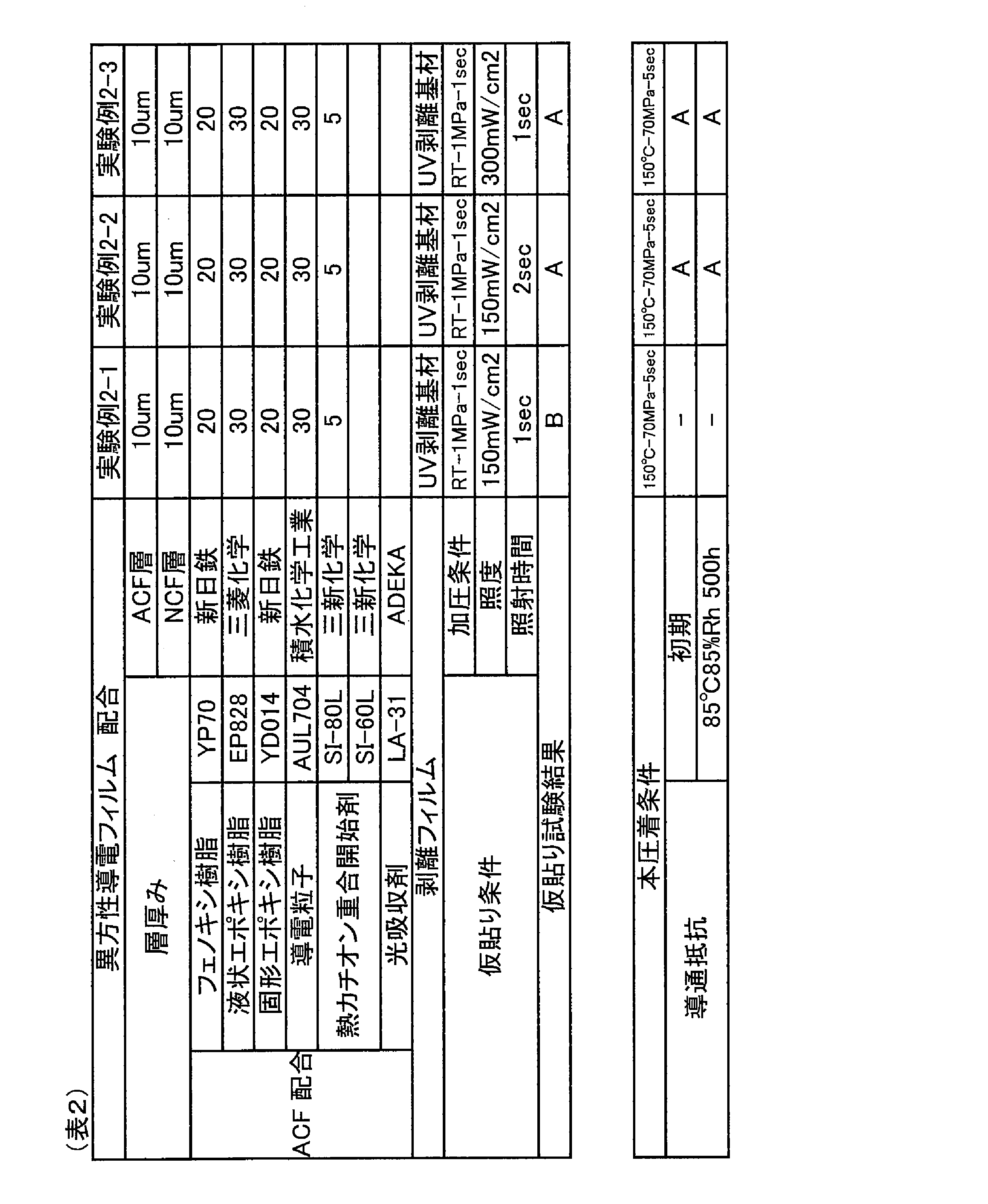

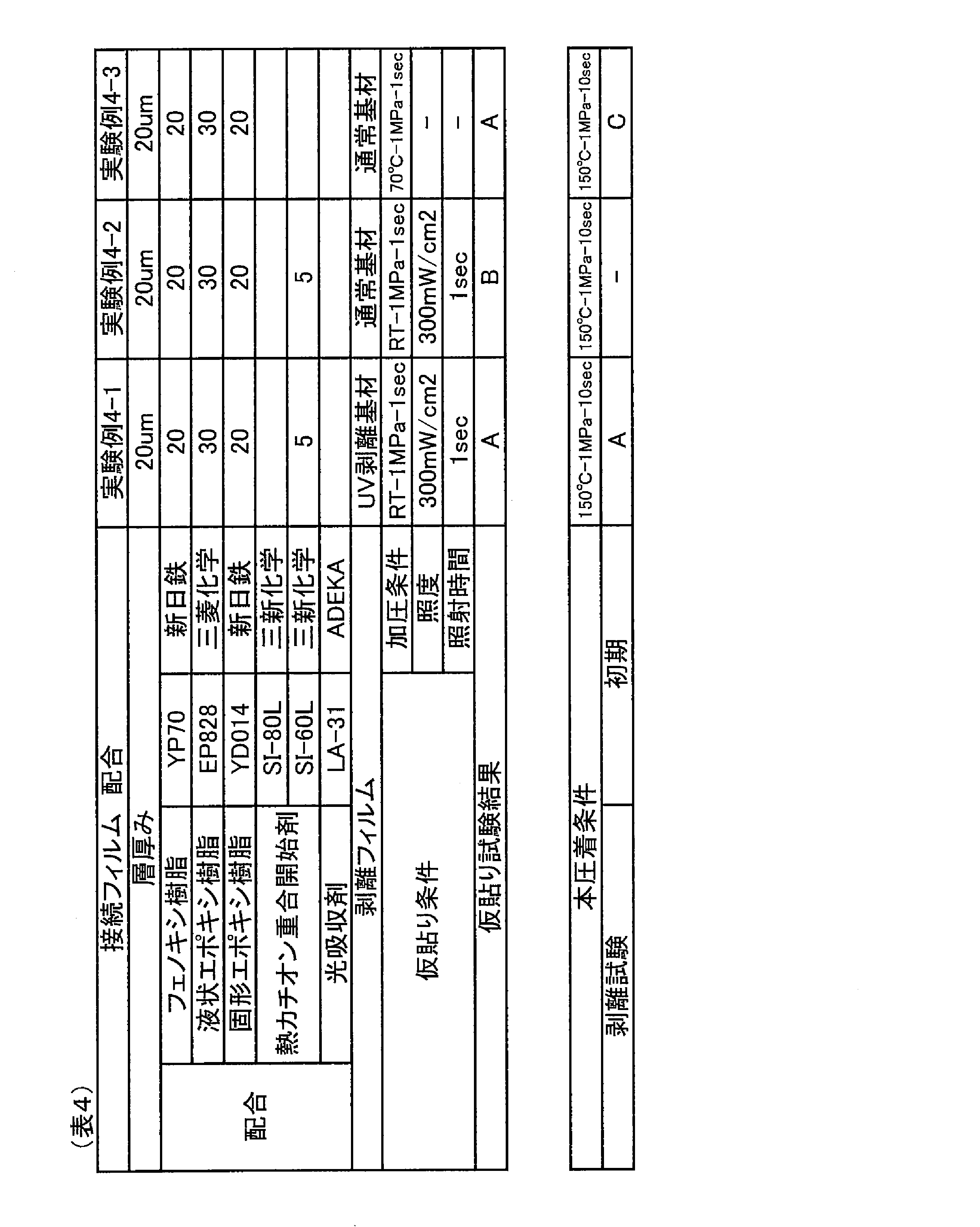
以上、添付図面を参照しながら本発明の好適な実施形態について詳細に説明したが、本発明はかかる例に限定されない。本発明の属する技術の分野における通常の知識を有する者であれば、特許請求の範囲に記載された技術的思想の範疇内において、各種の変更例または修正例に想到し得ることは明らかであり、これらについても、当然に本発明の技術的範囲に属するものと了解される。
10 接続フィルム
20 剥離フィルム
30 第1の電子部品
40 第2の電子部品
100 仮貼り用ツールヘッド
200、200a 緩衝材
300 本圧着用ツールヘッド
600 光源
20 剥離フィルム
30 第1の電子部品
40 第2の電子部品
100 仮貼り用ツールヘッド
200、200a 緩衝材
300 本圧着用ツールヘッド
600 光源
Claims (15)
- 接続フィルムを用いて第1の部品と第2の部品とを接続する接続構造体の製造方法であって、
前記接続フィルムの一方の面には剥離フィルムが設けられ、
前記接続フィルムの他方の面が前記第1の部品に接触するように前記接続フィルムを前記第1の部品上に搭載する工程と、
前記接続フィルムに光を照射することで、前記接続フィルムを前記第1の部品に仮貼りする工程と、
前記剥離フィルムを前記接続フィルムから剥離する工程と、
前記接続フィルム上に第2の部品を搭載する工程と、
前記接続フィルムを加熱しながら前記第2の部品を加圧することで、前記第1の部品と前記第2の部品とを本圧着する工程と、を含むことを特徴とする、接続構造体の製造方法。 - 前記接続フィルムは、加熱及び光照射のいずれかによって硬化可能な樹脂であるか、または熱可塑性樹脂で構成されることを特徴とする、請求項1記載の接続構造体の製造方法。
- 前記接続フィルムは、重合性化合物と、加熱により前記重合性化合物の硬化を開始させる熱硬化開始剤と、光照射により前記重合性化合物の硬化を開始させる光硬化開始剤とを含むことを特徴とする、請求項1または2に記載の接続構造体の製造方法。
- 前記接続フィルムは、重合性化合物と、加熱および光照射のいずれによっても前記重合性化合物の硬化を開始させる熱光硬化開始剤とを含むことを特徴とする、請求項1または2に記載の接続構造体の製造方法。
- 前記接続フィルムは、光照射により前記重合性化合物の硬化を開始させる光硬化開始剤をさらに含むことを特徴とする、請求項4記載の接続構造体の製造方法。
- 前記接続フィルムは、光照射によって発熱する光吸収剤を含むことを特徴とする、請求項1または2に記載の接続構造体の製造方法。
- 前記剥離フィルムと前記接続フィルムとの剥離強度は、光照射によって低下することを特徴とする、請求項1または2に記載の接続構造体の製造方法。
- 前記第1の部品および前記第2の部品は電子部品であり、
前記接続フィルムは、導電性粒子を含むことを特徴とする、請求項1または2に記載の接続構造体の製造方法。 - 第1の部品と第2の部品とを接続するための接続フィルムであって、
前記接続フィルムは、剥離フィルム上に形成され、
前記剥離フィルムと前記接続フィルムとの剥離強度は、光照射によって低下することを特徴とする、接続フィルム。 - 前記接続フィルムは、加熱及び光照射のいずれかによって硬化可能な樹脂であるか、または熱可塑性樹脂で構成されることを特徴とする、請求項9記載の接続フィルム。
- 前記接続フィルムは、重合性化合物と、加熱により前記重合性化合物の硬化を開始させる熱硬化開始剤と、光照射により前記重合性化合物の硬化を開始させる光硬化開始剤とを含むことを特徴とする、請求項9または10に記載の接続フィルム。
- 前記接続フィルムは、重合性化合物と、加熱および光照射のいずれによっても前記重合性化合物の硬化を開始させる熱光硬化開始剤とを含むことを特徴とする、請求項9または10に記載の接続フィルム。
- 前記接続フィルムは、光照射により前記重合性化合物の硬化を開始させる光硬化開始剤をさらに含むことを特徴とする、請求項12記載の接続フィルム。
- 前記接続フィルムは、光照射によって発熱する光吸収剤を含むことを特徴とする、請求項9または10に記載の接続フィルム。
- 前記第1の部品および前記第2の部品は電子部品であり、
前記接続フィルムは、導電性粒子を含むことを特徴とする、請求項9または10に記載の接続フィルム。
Priority Applications (2)
| Application Number | Priority Date | Filing Date | Title |
|---|---|---|---|
| KR1020217004274A KR102524175B1 (ko) | 2018-09-07 | 2019-08-31 | 접속 구조체의 제조 방법 및 접속 필름 |
| CN201980054359.8A CN112543795B (zh) | 2018-09-07 | 2019-08-31 | 连接结构体的制备方法及连接膜 |
Applications Claiming Priority (2)
| Application Number | Priority Date | Filing Date | Title |
|---|---|---|---|
| JP2018-168304 | 2018-09-07 | ||
| JP2018168304A JP7765164B2 (ja) | 2018-09-07 | 2018-09-07 | 接続構造体の製造方法および接続フィルム |
Publications (1)
| Publication Number | Publication Date |
|---|---|
| WO2020050188A1 true WO2020050188A1 (ja) | 2020-03-12 |
Family
ID=69722293
Family Applications (1)
| Application Number | Title | Priority Date | Filing Date |
|---|---|---|---|
| PCT/JP2019/034314 Ceased WO2020050188A1 (ja) | 2018-09-07 | 2019-08-31 | 接続構造体の製造方法および接続フィルム |
Country Status (5)
| Country | Link |
|---|---|
| JP (1) | JP7765164B2 (ja) |
| KR (1) | KR102524175B1 (ja) |
| CN (1) | CN112543795B (ja) |
| TW (1) | TWI837173B (ja) |
| WO (1) | WO2020050188A1 (ja) |
Families Citing this family (1)
| Publication number | Priority date | Publication date | Assignee | Title |
|---|---|---|---|---|
| JP7722886B2 (ja) * | 2021-09-22 | 2025-08-13 | 株式会社東芝 | 基板用仮接着剤及び基板加工方法 |
Citations (7)
| Publication number | Priority date | Publication date | Assignee | Title |
|---|---|---|---|---|
| JPH11191320A (ja) * | 1997-12-26 | 1999-07-13 | Sony Chem Corp | 異方性導電接着フィルム |
| JP2003064324A (ja) * | 2001-06-11 | 2003-03-05 | Hitachi Chem Co Ltd | 異方導電性接着フィルム及びそれを用いた回路基板の接続方法、回路基板接続体 |
| JP2013014755A (ja) * | 2011-06-10 | 2013-01-24 | Sekisui Chem Co Ltd | 異方性導電材料、接続構造体及び接続構造体の製造方法 |
| WO2015083809A1 (ja) * | 2013-12-05 | 2015-06-11 | デクセリアルズ株式会社 | 接続構造体の製造方法、及び異方性導電フィルム |
| JP2016042541A (ja) * | 2014-08-18 | 2016-03-31 | デクセリアルズ株式会社 | 接続構造体の製造方法、及び異方性導電接着フィルム |
| WO2017104417A1 (ja) * | 2015-12-14 | 2017-06-22 | デクセリアルズ株式会社 | 接続方法 |
| WO2018180685A1 (ja) * | 2017-03-30 | 2018-10-04 | デクセリアルズ株式会社 | 異方性導電接着剤及び接続体の製造方法 |
Family Cites Families (6)
| Publication number | Priority date | Publication date | Assignee | Title |
|---|---|---|---|---|
| JP4666550B2 (ja) | 2001-02-26 | 2011-04-06 | 日東電工株式会社 | 剥離ライナー付き加熱接着シート |
| JP4836475B2 (ja) | 2005-03-25 | 2011-12-14 | リンテック株式会社 | 基材レス両面粘着シート |
| JP4933157B2 (ja) | 2006-06-02 | 2012-05-16 | 東レエンジニアリング株式会社 | 異方性導電テープ貼付装置 |
| JP2011017011A (ja) | 2010-08-26 | 2011-01-27 | Hitachi Chem Co Ltd | 異方導電性接着フィルムの仮圧着方法 |
| JP6029922B2 (ja) | 2012-10-05 | 2016-11-24 | デクセリアルズ株式会社 | 回路接続材料及びその製造方法、並びにそれを用いた実装体の製造方法 |
| JP2014096531A (ja) * | 2012-11-12 | 2014-05-22 | Dexerials Corp | 接続構造体の製造方法及び接続方法 |
-
2018
- 2018-09-07 JP JP2018168304A patent/JP7765164B2/ja active Active
-
2019
- 2019-08-31 WO PCT/JP2019/034314 patent/WO2020050188A1/ja not_active Ceased
- 2019-08-31 KR KR1020217004274A patent/KR102524175B1/ko active Active
- 2019-08-31 CN CN201980054359.8A patent/CN112543795B/zh active Active
- 2019-09-05 TW TW108132043A patent/TWI837173B/zh active
Patent Citations (7)
| Publication number | Priority date | Publication date | Assignee | Title |
|---|---|---|---|---|
| JPH11191320A (ja) * | 1997-12-26 | 1999-07-13 | Sony Chem Corp | 異方性導電接着フィルム |
| JP2003064324A (ja) * | 2001-06-11 | 2003-03-05 | Hitachi Chem Co Ltd | 異方導電性接着フィルム及びそれを用いた回路基板の接続方法、回路基板接続体 |
| JP2013014755A (ja) * | 2011-06-10 | 2013-01-24 | Sekisui Chem Co Ltd | 異方性導電材料、接続構造体及び接続構造体の製造方法 |
| WO2015083809A1 (ja) * | 2013-12-05 | 2015-06-11 | デクセリアルズ株式会社 | 接続構造体の製造方法、及び異方性導電フィルム |
| JP2016042541A (ja) * | 2014-08-18 | 2016-03-31 | デクセリアルズ株式会社 | 接続構造体の製造方法、及び異方性導電接着フィルム |
| WO2017104417A1 (ja) * | 2015-12-14 | 2017-06-22 | デクセリアルズ株式会社 | 接続方法 |
| WO2018180685A1 (ja) * | 2017-03-30 | 2018-10-04 | デクセリアルズ株式会社 | 異方性導電接着剤及び接続体の製造方法 |
Also Published As
| Publication number | Publication date |
|---|---|
| CN112543795B (zh) | 2023-10-27 |
| CN112543795A (zh) | 2021-03-23 |
| KR20210034019A (ko) | 2021-03-29 |
| JP2020041032A (ja) | 2020-03-19 |
| TWI837173B (zh) | 2024-04-01 |
| TW202028390A (zh) | 2020-08-01 |
| KR102524175B1 (ko) | 2023-04-20 |
| JP7765164B2 (ja) | 2025-11-06 |
Similar Documents
| Publication | Publication Date | Title |
|---|---|---|
| WO2005002002A1 (ja) | 回路接続材料、これを用いたフィルム状回路接続材料、回路部材の接続構造及びその製造方法 | |
| WO2012137754A1 (ja) | 異方性導電フィルム、接合体の製造方法、及び接合体 | |
| JP2014096531A (ja) | 接続構造体の製造方法及び接続方法 | |
| TW201739327A (zh) | 連接結構體之製造方法 | |
| CN107432084A (zh) | 各向异性导电连接结构体、各向异性导电连接方法和各向异性导电粘接剂 | |
| JP5608426B2 (ja) | 異方性導電膜の製造方法 | |
| KR101973823B1 (ko) | 이방성 도전 접속 재료, 필름 적층체, 접속 방법 및 접속 구조체 | |
| TWI540195B (zh) | A circuit connecting material and a connecting method using the same, and a connecting structure | |
| TWI648156B (zh) | 異向性導電膜及其製造方法 | |
| TWI627639B (zh) | Electrical connecting material and manufacturing method thereof, and connecting body | |
| KR102524175B1 (ko) | 접속 구조체의 제조 방법 및 접속 필름 | |
| WO2018150897A1 (ja) | 異方性導電接続構造体、異方性導電接続構造体の製造方法、異方性導電フィルム、及び異方性導電ペースト | |
| JP6233069B2 (ja) | 異方性導電フィルム及びその製造方法 | |
| KR20180040667A (ko) | 접속 방법 | |
| JP7386773B2 (ja) | 異方性導電接着剤、接続構造体、異方性導電接続方法、及び接続構造体の製造方法 | |
| JP6431572B2 (ja) | 接続フィルム、接続フィルムの製造方法、接続構造体、接続構造体の製造方法及び接続方法 | |
| JP6177642B2 (ja) | 接続フィルム、接続構造体、接続構造体の製造方法、接続方法 | |
| HK1103169B (en) | Anisotropic conduction connecting method and anisotropic conduction adhesive film | |
| HK1103169A1 (en) | Anisotropic conduction connecting method and anisotropic conduction adhesive film | |
| JP2017098413A (ja) | リペア方法、及び接続方法 |
Legal Events
| Date | Code | Title | Description |
|---|---|---|---|
| 121 | Ep: the epo has been informed by wipo that ep was designated in this application |
Ref document number: 19858260 Country of ref document: EP Kind code of ref document: A1 |
|
| DPE1 | Request for preliminary examination filed after expiration of 19th month from priority date (pct application filed from 20040101) | ||
| ENP | Entry into the national phase |
Ref document number: 20217004274 Country of ref document: KR Kind code of ref document: A |
|
| NENP | Non-entry into the national phase |
Ref country code: DE |
|
| 122 | Ep: pct application non-entry in european phase |
Ref document number: 19858260 Country of ref document: EP Kind code of ref document: A1 |