WO2020031615A1 - 配線回路基板集合体シートおよびその製造方法 - Google Patents
配線回路基板集合体シートおよびその製造方法 Download PDFInfo
- Publication number
- WO2020031615A1 WO2020031615A1 PCT/JP2019/027676 JP2019027676W WO2020031615A1 WO 2020031615 A1 WO2020031615 A1 WO 2020031615A1 JP 2019027676 W JP2019027676 W JP 2019027676W WO 2020031615 A1 WO2020031615 A1 WO 2020031615A1
- Authority
- WO
- WIPO (PCT)
- Prior art keywords
- circuit board
- printed circuit
- area
- assembly sheet
- wiring
- Prior art date
- Legal status (The legal status is an assumption and is not a legal conclusion. Google has not performed a legal analysis and makes no representation as to the accuracy of the status listed.)
- Ceased
Links
Images

Classifications
-
- H—ELECTRICITY
- H05—ELECTRIC TECHNIQUES NOT OTHERWISE PROVIDED FOR
- H05K—PRINTED CIRCUITS; CASINGS OR CONSTRUCTIONAL DETAILS OF ELECTRIC APPARATUS; MANUFACTURE OF ASSEMBLAGES OF ELECTRICAL COMPONENTS
- H05K3/00—Apparatus or processes for manufacturing printed circuits
- H05K3/02—Apparatus or processes for manufacturing printed circuits in which the conductive material is applied to the surface of the insulating support and is thereafter removed from such areas of the surface which are not intended for current conducting or shielding
- H05K3/06—Apparatus or processes for manufacturing printed circuits in which the conductive material is applied to the surface of the insulating support and is thereafter removed from such areas of the surface which are not intended for current conducting or shielding the conductive material being removed chemically or electrolytically, e.g. by photo-etch process
-
- H—ELECTRICITY
- H05—ELECTRIC TECHNIQUES NOT OTHERWISE PROVIDED FOR
- H05K—PRINTED CIRCUITS; CASINGS OR CONSTRUCTIONAL DETAILS OF ELECTRIC APPARATUS; MANUFACTURE OF ASSEMBLAGES OF ELECTRICAL COMPONENTS
- H05K1/00—Printed circuits
- H05K1/02—Details
-
- H—ELECTRICITY
- H05—ELECTRIC TECHNIQUES NOT OTHERWISE PROVIDED FOR
- H05K—PRINTED CIRCUITS; CASINGS OR CONSTRUCTIONAL DETAILS OF ELECTRIC APPARATUS; MANUFACTURE OF ASSEMBLAGES OF ELECTRICAL COMPONENTS
- H05K2201/00—Indexing scheme relating to printed circuits covered by H05K1/00
- H05K2201/09—Shape and layout
- H05K2201/09209—Shape and layout details of conductors
- H05K2201/09654—Shape and layout details of conductors covering at least two types of conductors provided for in H05K2201/09218 - H05K2201/095
- H05K2201/09781—Dummy conductors, i.e. not used for normal transport of current; Dummy electrodes of components
-
- H—ELECTRICITY
- H05—ELECTRIC TECHNIQUES NOT OTHERWISE PROVIDED FOR
- H05K—PRINTED CIRCUITS; CASINGS OR CONSTRUCTIONAL DETAILS OF ELECTRIC APPARATUS; MANUFACTURE OF ASSEMBLAGES OF ELECTRICAL COMPONENTS
- H05K2203/00—Indexing scheme relating to apparatus or processes for manufacturing printed circuits covered by H05K3/00
- H05K2203/05—Patterning and lithography; Masks; Details of resist
- H05K2203/0562—Details of resist
-
- H—ELECTRICITY
- H05—ELECTRIC TECHNIQUES NOT OTHERWISE PROVIDED FOR
- H05K—PRINTED CIRCUITS; CASINGS OR CONSTRUCTIONAL DETAILS OF ELECTRIC APPARATUS; MANUFACTURE OF ASSEMBLAGES OF ELECTRICAL COMPONENTS
- H05K2203/00—Indexing scheme relating to apparatus or processes for manufacturing printed circuits covered by H05K3/00
- H05K2203/13—Moulding and encapsulation; Deposition techniques; Protective layers
- H05K2203/1377—Protective layers
- H05K2203/1383—Temporary protective insulating layer
-
- H—ELECTRICITY
- H05—ELECTRIC TECHNIQUES NOT OTHERWISE PROVIDED FOR
- H05K—PRINTED CIRCUITS; CASINGS OR CONSTRUCTIONAL DETAILS OF ELECTRIC APPARATUS; MANUFACTURE OF ASSEMBLAGES OF ELECTRICAL COMPONENTS
- H05K2203/00—Indexing scheme relating to apparatus or processes for manufacturing printed circuits covered by H05K3/00
- H05K2203/14—Related to the order of processing steps
- H05K2203/1461—Applying or finishing the circuit pattern after another process, e.g. after filling of vias with conductive paste, after making printed resistors
-
- H—ELECTRICITY
- H05—ELECTRIC TECHNIQUES NOT OTHERWISE PROVIDED FOR
- H05K—PRINTED CIRCUITS; CASINGS OR CONSTRUCTIONAL DETAILS OF ELECTRIC APPARATUS; MANUFACTURE OF ASSEMBLAGES OF ELECTRICAL COMPONENTS
- H05K2203/00—Indexing scheme relating to apparatus or processes for manufacturing printed circuits covered by H05K3/00
- H05K2203/14—Related to the order of processing steps
- H05K2203/1476—Same or similar kind of process performed in phases, e.g. coarse patterning followed by fine patterning
-
- H—ELECTRICITY
- H05—ELECTRIC TECHNIQUES NOT OTHERWISE PROVIDED FOR
- H05K—PRINTED CIRCUITS; CASINGS OR CONSTRUCTIONAL DETAILS OF ELECTRIC APPARATUS; MANUFACTURE OF ASSEMBLAGES OF ELECTRICAL COMPONENTS
- H05K2203/00—Indexing scheme relating to apparatus or processes for manufacturing printed circuits covered by H05K3/00
- H05K2203/15—Position of the PCB during processing
- H05K2203/1509—Horizontally held PCB
-
- H—ELECTRICITY
- H05—ELECTRIC TECHNIQUES NOT OTHERWISE PROVIDED FOR
- H05K—PRINTED CIRCUITS; CASINGS OR CONSTRUCTIONAL DETAILS OF ELECTRIC APPARATUS; MANUFACTURE OF ASSEMBLAGES OF ELECTRICAL COMPONENTS
- H05K2203/00—Indexing scheme relating to apparatus or processes for manufacturing printed circuits covered by H05K3/00
- H05K2203/16—Inspection; Monitoring; Aligning
- H05K2203/166—Alignment or registration; Control of registration
-
- H—ELECTRICITY
- H05—ELECTRIC TECHNIQUES NOT OTHERWISE PROVIDED FOR
- H05K—PRINTED CIRCUITS; CASINGS OR CONSTRUCTIONAL DETAILS OF ELECTRIC APPARATUS; MANUFACTURE OF ASSEMBLAGES OF ELECTRICAL COMPONENTS
- H05K3/00—Apparatus or processes for manufacturing printed circuits
- H05K3/02—Apparatus or processes for manufacturing printed circuits in which the conductive material is applied to the surface of the insulating support and is thereafter removed from such areas of the surface which are not intended for current conducting or shielding
- H05K3/06—Apparatus or processes for manufacturing printed circuits in which the conductive material is applied to the surface of the insulating support and is thereafter removed from such areas of the surface which are not intended for current conducting or shielding the conductive material being removed chemically or electrolytically, e.g. by photo-etch process
- H05K3/067—Etchants
Definitions
- the present invention relates to a printed circuit board assembly sheet and a method for manufacturing the same.
- a dummy pattern restricts the flow of an etchant, thereby suppressing the amount of side etching progressing between lines and securing a desired line width in a circuit pattern.
- Patent Document 1 it is necessary to first specify the above-mentioned wide line intervals in a plurality of lines, and to arrange a resist film corresponding to the dummy pattern for each of the positions, which is complicated.
- the present invention provides a method for manufacturing a printed circuit board assembly sheet, which can easily manufacture a printed circuit board with high reliability, and a printed circuit board assembly sheet obtained by the method.
- wiring including a conductive layer, A support substrate made of a metal-based layer is formed by etching.
- the etching resist is arranged in the product region and the etching is performed, the etching solution reaches the margin region while forming the wiring and the support substrate while the etching solution is in contact with the etching resist.
- the margin area has a first area adjacent to the product area and a second area located on the opposite side of the product area with respect to the first area. Since the substrate is arranged in at least a part of the first area, the accuracy of the dummy wiring circuit board is reduced even if the etchant drops when the etchant reaches the second area from the product area, causing turbulence. However, since the influence of the turbulent flow of the etchant on the printed circuit board is reduced, a decrease in the precision of the printed circuit board is suppressed. Therefore, in the printed circuit board assembly sheet, the reliability of the printed circuit board is excellent.
- the present invention (2) includes the wired circuit board assembly sheet according to (1), wherein the dummy wired circuit board is arranged over the entire first area.
- the wiring circuit according to (1) or (2), wherein the printed circuit board includes wiring formed of a conductor layer, and the dummy printed circuit board includes dummy wiring formed of the conductor layer. includes a substrate assembly sheet.
- the conductor layer corresponding to the wiring and the dummy wiring is used in manufacturing the printed circuit board assembly sheet.
- An etching resist When the etchant drops from the first area to the second area and the etchant drops, causing turbulence, the accuracy of the dummy wiring is reduced, but the reduction in the precision of the wiring is suppressed. Therefore, the wiring circuit board assembly sheet has excellent wiring reliability.
- the wiring circuit assembly sheet has a long shape, is included in the second area, has both ends in the width direction orthogonal to the long direction, and both ends in the width direction.
- the wiring circuit assembly sheet has a long shape, the wiring circuit board assembly sheet is etched and manufactured while being transported in the long direction.
- the present invention (5) provides the printed circuit board according to any one of (1) to (4), wherein the printed circuit board includes a support substrate formed of a metal-based layer, and the dummy printed circuit board includes a dummy support substrate formed of the metal-based layer.
- the printed circuit board assembly sheet according to any one of the preceding claims.
- the manufacturing method of the printed circuit board assembly sheet includes the support substrate and the dummy support substrate.
- An etching resist is arranged on the metal-based layer corresponding to the above.
- the wiring circuit assembly sheet may have a long shape, and may be included in the second area and have both ends in the width direction orthogonal to the long direction, and both ends in the width direction.
- the wiring circuit assembly sheet has a long shape, the wiring circuit board assembly sheet is etched and manufactured while being transported in the long direction.
- the present invention (7) is a wiring circuit assembly sheet in which a product area in which a plurality of wiring circuit boards as products are aligned and a margin area surrounding the product area are partitioned.
- the wiring circuit assembly sheet includes a wiring formed of a conductive layer, the wiring circuit assembly sheet has a long shape, is included in the margin area, has width direction both ends orthogonal to the long direction, and has both ends in the width direction.
- a printed circuit board assembly sheet provided with a conductor end made of the conductor layer.
- the present invention (8) is a wiring circuit assembly sheet that divides a product area in which a plurality of wiring circuit boards as products are arranged and a margin area surrounding the product area, wherein the wiring circuit board includes:
- the wiring circuit assembly sheet includes a support substrate made of a metal-based layer, the wiring circuit assembly sheet has a long shape, is included in the margin area, has both ends in a width direction orthogonal to the long direction, and has a width
- the printed circuit board assembly sheet includes metal-based ends that are disposed at both ends in the direction and that includes the metal-based layer.
- the present invention (9) is the method for manufacturing a wiring circuit assembly sheet according to (3), wherein a first etching resist is disposed on the conductor layer so as to correspond to the wiring and the dummy wiring.
- a method for manufacturing a wiring circuit board assembly sheet comprising one step and a second step of forming the wiring and the dummy wiring by etching the conductor layer exposed from the first etching resist.
- the first step if the first etching resist is disposed on the conductor layer so as to correspond to the wiring and the dummy wiring, the side etching of the dummy wiring caused by the turbulent flow of the etching solution in the first area is performed in the second step.
- the width of the dummy wiring cannot be sufficiently secured, the product region is hardly affected by the turbulence, and the width of the wiring can be sufficiently secured.
- the conductor layer may be conveyed along a conveyance direction in a second step, and may be included in the second area and have both ends in a width direction orthogonal to the conveyance direction.
- the first etching resist covers one side in the thickness direction of both ends in the width direction of the conductor layer, and protrudes from both ends in the width direction of the conductor layer to both outer sides in the width direction.
- the first etching resist is formed so as to cover one surface in the thickness direction of both ends in the width direction of the conductor layer and to protrude from both ends in the width direction to both outer sides in the width direction of the conductor layer.
- a place where the turbulence of the etching solution easily occurs can be kept away from the product area. Thereby, the influence of the disorder of the etching solution can be reduced in the product area.
- the present invention (11) is the method for producing a wiring circuit assembly sheet according to (5), wherein a second etching resist is applied to the metal-based layer so as to correspond to the support substrate and the dummy support substrate.
- Producing a wiring circuit board assembly sheet comprising: a third step of disposing; and a fourth step of etching the metal-based layer exposed from the second etching resist to form the support substrate and the dummy support substrate. Including methods.
- the first step if the first etching resist is disposed on the metal-based layer so as to correspond to the support substrate and the dummy support substrate, in the second step, the dummy support caused by the turbulent flow of the etchant in the first area is formed. Even if the width of the dummy support substrate cannot be sufficiently secured by the side etching of the substrate, the product region is hardly affected by the turbulence, and the width of the wiring can be sufficiently secured.
- the metal-based layer is transported in a transport direction in a fourth step, and is included in the second area and has both ends in a width direction orthogonal to the transport direction.
- the second etching resist covers one side in the thickness direction of both ends in the width direction of the metal-based layer, and extends from the both ends in the width direction to both outsides in the width direction of the metal-based layer.
- Etching is performed by forming the first etching resist so as to cover one surface in the thickness direction of both ends in the width direction of the metal-based layer and to project outward from both ends in the width direction of the metal-based layer.
- a place where the turbulence of the etchant is likely to occur can be kept away from the product area. Thereby, the influence of the disorder of the etching solution can be reduced in the product area.
- the printed circuit board assembly sheet of the present invention has excellent printed circuit board reliability.
- the method for manufacturing a printed circuit board assembly sheet of the present invention can easily manufacture a printed circuit board having excellent reliability.
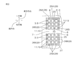
- FIG. 1 shows a plan view of a first embodiment of a printed circuit board assembly sheet of the present invention.
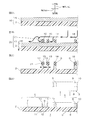
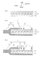
- 2A to 2D are manufacturing process diagrams of the printed circuit board assembly sheet shown in FIG. 1, and are cross-sectional views along the line AA in FIG. 1.
- FIG. Shows a resist disposing step
- FIG. 2C shows an etching step
- FIG. 2D shows a resist removing step and a cover step.
- FIG. 3 shows a plan view of a modification of the first embodiment.
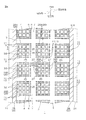
- FIG. 4 shows a plan view of the printed circuit board assembly sheet of the second embodiment.
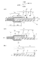
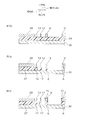
- 5A to 5C are cross-sectional views of the printed circuit board assembly sheet shown in FIG. 4 along the line AA in FIG. 4, where FIG. 5A is a resist arrangement step, and FIG. FIG.
- FIG. 5C shows a resist removing step and a cover step.
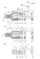
- 6A to 6C are manufacturing process diagrams (cross-sectional views) of the printed circuit board assembly sheet of the third embodiment.
- FIG. 6A shows a base material preparing process
- FIG. 6B shows a first resist disposing process
- FIG. One etching step is shown.
- 7 is a manufacturing process diagram (cross-sectional view) of the printed circuit board assembly sheet of the third embodiment, following FIG. 6C
- FIG. 7D shows a first resist removing process
- FIG. 7E shows a base layer forming process
- FIG. 7F shows the cover step.
- FIG. 8 is a manufacturing process diagram (cross-sectional view) of the printed circuit board assembly sheet according to the third embodiment, following FIG. 7F.
- FIG. 8G shows a second resist disposing process
- FIG. FIG. 7I shows the second resist removing step.
- a first embodiment of the printed circuit board assembly sheet of the present invention will be described with reference to FIGS. 1 to 2D.
- FIG. 1 is an enlarged view of the printed circuit board and the dummy printed circuit board, and the hatched figure in the lower right is a view in which each area is divided according to the type of hatching. .
- the printed circuit board assembly sheet 1 has a long sheet shape extending in the longitudinal direction.
- the printed circuit board assembly sheet 1 has a predetermined length in a width direction orthogonal to the longitudinal direction.
- the printed circuit board assembly sheet 1 has one surface and the other surface facing each other at an interval in a thickness direction orthogonal to the longitudinal direction and the width direction.
- the printed circuit board assembly sheet 1 includes a support sheet 2 and a plurality of printed circuit boards 3.
- the support sheet 2 has the same planar view shape (outer shape) as the printed circuit board assembly sheet 1.
- Examples of the material of the support sheet 2 include a resin such as polyimide.
- the thickness of the support sheet 2 is, for example, 1 ⁇ m or more and 1 mm or less.
- the printed circuit board 3 has a substantially rectangular shape in plan view.
- a plurality of printed circuit boards 3 are arranged on the support sheet 2.
- Each of the plurality of printed circuit boards 3 is supported on the support sheet 2 so as to be separable.
- an opening 14 is formed around the printed circuit board 3, and the printed circuit board 3 is Are connected to the support sheet 2.
- the opening 14 has a substantially rectangular frame shape surrounding the printed circuit board 3 in a plan view, and penetrates in the thickness direction of the support sheet 2.
- the joint 24 crosses the opening 14, thereby suspending the support sheet 2 on the printed circuit board 3.
- the joint 24 has the same material and thickness as the support sheet 2.
- the layer configuration of the printed circuit board 3 will be described later.
- the printed circuit board 3 is a product in the printed circuit board assembly sheet 1 unlike the dummy printed circuit board 11 described later.
- a product area 4 and a margin area 5 are defined.
- the product region 4 is a region partitioned into a substantially rectangular shape in a plan view, and in the printed circuit board assembly sheet 1, a sufficient interval between each other in the longitudinal direction and the width direction (specifically, a margin region 5 described later is formed). (Provided area).
- the plurality of printed circuit boards 3 are arranged and arranged with a slight gap 25 therebetween. More specifically, in the product area 4, the adjacent printed circuit boards 3 are separated from each other by minute gaps 25, and the gaps 25 improve the yield of the printed circuit boards 3 in the printed circuit board assembly sheet 1. From the viewpoint, it is set as small (narrow) as possible.
- the ratio of the length (width) of the gap 25 separating the adjacent printed circuit boards 3 to the width of the printed circuit board 3 is, for example, 0.1 or less, preferably 0.01 or less, more preferably 0.001 or less. And, for example, 0.0001 or more.
- the length (width) of the gap 25 separating the adjacent printed circuit boards 3 is, for example, 100 ⁇ m or less, preferably 50 ⁇ m or less, more preferably 10 ⁇ m or less, and for example, 0.1 ⁇ m or less. That is all.
- all the gaps 25 have the same width. That is, the printed circuit boards 3 are arranged and arranged with the gap 25 having the same width therebetween.
- the margin region 5 surrounds the product region 4.
- the margin region 5 has a substantially rectangular frame shape surrounding one product region 4.
- the margin region 5 has a substantially cross-girder shape and a band-like shape extending in the longitudinal direction along both edges in the width direction of the support sheet 2 in plan view in the printed circuit board assembly sheet 1. . That is, regarding the margin region 5 having a substantially cross-girder shape, one margin region 5 corresponding to one product region 4A and another margin region 5 corresponding to another product region 4B adjacent to the one product region 4A are different from each other. , Is continuous.
- the margin area 5 has a first area 6 and a second area 7.
- the first area 6 is hatched by oblique lines from upper left to lower right
- the second area 7 is hatched by oblique lines from upper right to lower left.
- the first area 6 is adjacent to the product area 4. Specifically, the first area 6 is arranged near the product region 4, that is, close to the periphery of the product region 4.
- the first area 6 is divided into a substantially rectangular frame shape in plan view that surrounds the vicinity just outside the product area 4. That is, the inner size of the first area 6 is set substantially equal to the outer size of the product area 4.
- a dummy wiring circuit board 11 described later is arranged in the first area 6.
- the second area 7 is located on the opposite side of the product area 4 with respect to the first area 6. That is, the second area 7 is remote from the product area 4 via the first area 6. In other words, the second area 7 surrounds the first area 6.
- the second area 7 is divided into a substantially rectangular frame shape in plan view surrounding the area immediately outside the first area 6. That is, the inner size of the second area 7 is set to be substantially the same as the outer size of the first area 6.
- the second area 7 located between the two adjacent product areas 4A and 4B is shared by the two product areas 4A and 4B.
- the second area 7 is defined as a blank area in the margin area 5.
- the first area 6 and the second area 7 are arranged in order toward the outside of the product area 4 (outside in the plane perpendicular to the thickness direction).
- the margin region 5 does not include the gap 25 in the product region 4, that is, is distinguished from the gap 25.
- the width of the margin region 5 is sufficiently large.
- the ratio of the width of the margin region 5 to the width of the product region 4 is, for example, 10 or more. It is preferably at least 100, more preferably at least 1,000, and for example, at most 100,000.
- the width of the margin region 5 between the product regions 4A and 4B adjacent in the width direction is the length in the width direction.
- the width of the margin region 5 between the product regions 4A and 4C adjacent in the longitudinal direction is the longitudinal length.
- the width of the margin region 5 located on the outermost side in the width direction is the widthwise length between the widthwise edge of the margin region 5 and the product region 4A (or 4C) located on the outermost side in the widthwise direction.
- the width direction length, the length direction length, and the like of the margin region 5 can be collectively referred to as the width direction of the margin region 5.
- the length in the short direction of the margin region 5 is, for example, 5 mm or more, preferably 10 mm or more, more preferably 20 mm or more, and is, for example, 50 mm or less.
- the printed circuit board 3 covers the base layer 8, the wiring 9 disposed on one surface in the thickness direction of the base layer 8, and the wiring 9 on one surface in the thickness direction of the base layer 8. And a cover layer 10 (virtual line) disposed on the second side.
- the base layer 8 has the same planar shape as the printed circuit board 3.
- the base layer 8 is separated from the surrounding support sheet 2 by an opening 14 (see FIG. 1).
- the material and thickness of the base layer 8 are the same as those of the support sheet 2.
- the wiring 9 has a pattern included in the base layer 8 in a plan view.
- the pattern shape of the wiring 9 is not particularly limited, and is appropriately set according to the application and purpose.
- the wiring 9 includes, for example, a signal line (such as a differential wiring), a power line (such as a power wiring), a ground line (such as a ground line), an antenna line (such as a transmission / reception line), and the like.
- the wiring 9 may further include, for example, an auxiliary unit (a terminal or the like) (not illustrated) corresponding to the function of each wiring described above in a plan view.
- the wiring 9 is made of a conductor layer 15 (see FIGS. 2A and 2B) described later.
- Examples of the material of the wiring 9 include a conductor such as a metal-based material (specifically, a metal material).
- a metal-based material include metal elements classified into Groups 1 to 16 in the periodic table and alloys containing two or more of these metal elements.
- the metal-based material may be either a transition metal or a typical metal. More specifically, examples of the metal-based material include Group 2 metal elements such as calcium, Group 4 metal elements such as titanium and zirconium, Group 5 metal elements such as vanadium, chromium, molybdenum, and tungsten.
- Group 6 metal elements Group 7 metal elements such as manganese, Group 8 metal elements such as iron, Group 9 metal elements such as cobalt, Group 10 metal elements such as nickel and platinum, copper, silver, gold, etc.
- Group 11 metal element a Group 12 metal element such as zinc, a Group 13 metal element such as aluminum and gallium, and a Group 14 metal element such as germanium and tin. These can be used alone or in combination.
- the ratio of the thickness of the wiring 9 to the thickness of the base layer 8 is, for example, 0.5 or more, preferably 1.0 or more, more preferably 1.5 or more, and for example, 3.0 or less. is there. Specifically, the thickness of the wiring 9 is, for example, 1 ⁇ m or more and 1000 ⁇ m or less.
- the width of the wiring 9 is, for example, not less than 10 ⁇ m and not more than 1000 ⁇ m.
- the cover layer 10 covers one surface of the base layer 8 exposed from the wiring 9 and the side surface and one surface in the thickness direction of the wiring 9.
- the material of the cover layer 10 is the same as the material of the base layer 8.
- the ratio of the thickness of the cover layer 10 to the thickness of the base layer 8 is, for example, 0.2 or more, preferably 0.3 or more, more preferably 0.5 or more, and, for example, 2.0 or less. It is. Specifically, the thickness of the cover layer 10 is, for example, not less than 25 ⁇ m and not more than 1000 ⁇ m.
- the dummy wiring circuit board 11 is arranged in the first area 6. Specifically, the dummy wiring circuit board 11 is arranged in the entire first area 6. Specifically, in the first area 6, a plurality of the dummy wiring circuit boards 11 are arranged in a line along the frame forming the first area 6 at intervals.
- the dummy wiring circuit board 11 includes a first dummy wiring circuit board 26 arranged on both sides in the longitudinal direction and a width direction of the product region 4 and a second dummy wiring board arranged diagonally outside the product region 4. And a circuit board 27.
- the first dummy wiring circuit boards 26A arranged on both sides in the longitudinal direction of the product region 4 are arranged in one row at intervals in the width direction.
- the pitch in the width direction of the first dummy wiring circuit board 26A and the pitch in the width direction of the wiring circuit board 3 are the same.
- the length and the interval in the width direction of the first dummy wiring circuit board 26A are the same as the length and the interval in the width direction of the wiring circuit board 3 respectively.
- the longitudinal length L1 of the first dummy wired circuit board 26A and the longitudinal length L0 of the wired circuit board 3 satisfy, for example, the following expression (5), and preferably satisfy the following expression (6). Satisfies, more preferably, satisfies the following expression (7), and satisfies the following expression (8).
- L1 ⁇ L0 (5) L1 ⁇ 0.5 ⁇ L0 (6)
- the first dummy wiring circuit boards 26B arranged on both sides in the width direction of the product region 4 are arranged in one row at intervals in the longitudinal direction.
- the longitudinal pitch of the first dummy printed circuit board 26B and the longitudinal pitch of the printed circuit board 3 are the same. Specifically, the length and the interval in the longitudinal direction of the first dummy wired circuit board 26B are the same as the length and the interval in the longitudinal direction of the wired circuit board 3 respectively.
- the width direction length W1 of the first dummy wiring circuit board 26B and the width direction length W0 of the wiring circuit board 3 satisfy, for example, the following expression (9), and preferably satisfy the following expression (10). Satisfies, more preferably, satisfies the following expression (11), and also satisfies the following expression (12).
- W1 ⁇ W0 (9) W1 ⁇ 0.5 ⁇ W0 (10) W1 ⁇ 0.25 ⁇ W0 (11) 0.001 ⁇ W0 ⁇ W1 (12)
- the second dummy wiring circuit board 27 is smaller than the first dummy wiring circuit board 26.
- the length L2 and the width W2 of the second dummy wiring circuit board 27 are respectively equal to the length L1 of the first dummy wiring circuit board 26A arranged on both sides in the longitudinal direction of the product area 4, and 4 is the same as the width W1 of the first dummy wiring circuit board 26B disposed on both sides in the width direction.
- the second dummy wiring circuit board 27 is arranged at each of the four corners of the frame forming the first area 6.
- the printed circuit board 3, the first dummy printed circuit board 26, and the second dummy printed circuit board 27 are separated by an equal interval (a minute gap 25). They are arranged.
- the dummy wiring circuit board 11 is smaller than the wiring circuit board 3. Specifically, the dummy printed circuit board 11 is smaller than the printed circuit board 3 in a plan view. More specifically, the plane area S1 of the dummy printed circuit board 11 and the plane area S0 of the printed circuit board 3 are expressed by the following formula. It satisfies (13), preferably satisfies the following expression (14), more preferably satisfies the following expression (15), and still more preferably satisfies the following expression (16).
- the dummy printed circuit board 11 has the same layer configuration as the printed circuit board 3, unlike the printed circuit board 3, the dummy printed circuit board 11 is not collected (collected) from the printed circuit board assembly sheet 1 as a product, and is supported by the support sheet 2. And remain in the state. That is, the dummy wiring circuit board 11 is not a product.
- the dummy wiring circuit board 11 includes a dummy base layer 12 and a dummy wiring 13 arranged on one surface of the dummy base layer 12 in the thickness direction.
- Dummy base layer 12 and dummy wiring 13 have the same layer configuration and thickness as base layer 8 and wiring 9 of printed circuit board 3.
- the dummy base layer 12 is partitioned by the openings 14 (see FIG. 1).
- Dummy wiring 13 is formed of conductor layer 15 # (see FIGS. 2A and 2B).
- the width of the dummy wiring 13 is allowed to be smaller than the width of the wiring 9.
- the width W6 of the dummy wiring 13 and the width W5 of the wiring 9 satisfy the following expression (17), and further satisfy the following expression (18).
- W6 ⁇ W5 (17) 0.01 ⁇ W5 ⁇ W6 ⁇ 0.5 ⁇ W5 (18)
- a method of manufacturing the printed circuit board assembly sheet 1 will be described.
- the method of manufacturing the printed circuit board assembly sheet 1 includes a base material preparing step, a resist arranging step as an example of a first step, an etching step as an example of a second step, and resist removal. Process and a cover process.
- the method of manufacturing the printed circuit board assembly sheet 1 is performed, for example, according to a roll-to-roll method.
- a roll-to-roll method in a device for manufacturing each layer (not shown), a take-up roll and a take-up roll ( Each of them is not shown), and in each step, each member that is unwound from the unwinding roll is unwound toward the take-up roll.
- a two-layer base material 16 including the support sheet 2 and the conductor layer 15 arranged on one surface in the thickness direction of the support sheet 2 is prepared.
- the two-layer substrate 16 preferably includes only the support sheet 2 and the conductor layer 15.
- the support sheet 2 has not been formed with the above-described opening 14 (see the upper right diagram in FIG. 1), and therefore, is a long sheet that is continuous in the longitudinal direction and has no opening 14. Be prepared.
- the conductor layer 15 is disposed on the entire surface of one side in the thickness direction of the support sheet 2.
- a pattern corresponding to the wirings 9 and the dummy wirings 13 has not been formed yet, and the conductive layer 15 is prepared as a long conductive sheet continuous in the longitudinal direction.
- the material and thickness of the conductor layer 15 are the same as those of the wiring 9 described above.
- a resin is applied to the other surface in the thickness direction of the conductor layer 15 and then dried to form the support sheet 2.
- a two-layer base material 16 provided in advance with the support sheet 2 and the conductor layer 15 can be prepared as it is.
- the first etching resist 17 is disposed on one surface in the thickness direction of the conductor layer 15 so as to correspond to the wiring 9 and the dummy wiring 13 (see FIG. 2C).
- first etching resist 17 is formed on the conductor layer 15, although not shown, for example, first, a sheet-like dry film resist is arranged on one entire surface of the conductor layer 15 in the thickness direction. Next, a first etching resist 17 is formed from the dry film resist by photolithography (exposure and development) so as to have a shape corresponding to the wiring 9 and the dummy wiring 13.
- the first etching resist 17 includes a resist product part 18 corresponding to the wiring 9 and a resist dummy part 19 corresponding to the dummy wiring 13.
- Each of the resist product section 18 and the resist dummy section 19 has the same width as the wiring 9 to be formed next in plan view.
- a resist laminate 20 including the support sheet 2, the conductor layer 15, and the first etching resist 17 in order toward one side in the thickness direction is manufactured.
- an etching apparatus (not shown) having a discharge port (a nozzle, a shower head, etc.) is used.
- the discharge ports (not shown) are arranged on one side in the thickness direction of the resist laminate 20, and are arranged in parallel in the width direction of the resist laminate 20. Are provided so as to oppose to each other.
- the etching solution comes in contact with the resist product portion 18 and the conductor layer 15 exposed from the discharge port, reaches the resist dummy portion 19 disposed outside the resist product portion 18, and then continues. As a result, it falls into the conductor layer 15 corresponding to the second area 7.
- the etchant spreads from the resist product portion 18 toward the resist dummy portion 19, and then, from the resist dummy portion 19, the etchant just before falling into the conductor layer 15 corresponding to the second area 7, that is, the resist dummy portion 19
- the turbulence occurs in the etching around. Therefore, the etching solution contacts the conductor layer 15 exposed from the resist dummy portion 19 at a high speed, so that the etching rate of the conductor layer 15 increases.
- an over-etched dummy wiring 13 is formed.
- the width of the dummy wiring 13 is smaller than the width of the resist dummy portion 19.
- the resist product portion 18 is disposed on the inner side of the resist dummy portion 19 with the resist dummy portion 19 interposed therebetween, so that the influence of the turbulence described above is small (it is hard to be affected).
- This suppresses the increase in the speed of the etchant caused by the above. Therefore, an increase in the etching rate is also suppressed, so that the above-described over-etching is suppressed.
- the width of the wiring 9 becomes the same as the width of the resist product portion 18. That is, the patterning accuracy of the wiring 9 is high.
- the first etching resist 17 is removed by, for example, peeling.
- the cover layer 10 is disposed on one side in the thickness direction of the support sheet 2 so as to cover one surface and side surfaces in the thickness direction of the wiring 9.
- the support sheet 2 is externally processed to form the opening 14.
- a joint 24 (see FIG. 1) is formed.
- the printed circuit board assembly sheet 1 is manufactured.
- the printed circuit board 3 is separated from the support sheet 2 and collected (collected) from the printed circuit board assembly sheet 1.
- the dummy wiring circuit board 11 remains supported by the support sheet 2 and is then discarded together with the support sheet 2.
- the etchant falls from the product region 4 to the second area 7, the etchant drops and the first area 6
- the accuracy of the dummy printed circuit board 11 arranged in the product region 4 is reduced, the influence of the turbulent flow of the etchant on the printed circuit board 3 is reduced. Is suppressed. Therefore, in the printed circuit board assembly sheet 1, the reliability of the printed circuit board 3 is excellent.
- the printed circuit board 3 includes the wiring 9 formed of the conductor layer 15, and the dummy printed circuit board 11 includes the dummy wiring 13 formed of the conductor layer 15. Therefore, in the manufacture of the printed circuit board assembly sheet 1, the first etching resist 17 is disposed on the conductor layer 15 corresponding to the wiring 9 and the dummy wiring 13. When the etchant drops from the first area 6 to the second area 7 and the etchant drops, causing turbulence, the accuracy of the dummy wiring 13 is reduced, but the reduction of the accuracy of the wiring 9 is suppressed. You. Therefore, in the wired circuit board assembly sheet 1, the reliability of the wiring 9 is excellent.
- the dummy wiring circuit board 11 is arranged over the entire first area 6, but the dummy wiring circuit board 11 may be arranged over a part of the first area 6. Good.
- the dummy wiring circuit board 11 has the first dummy wiring circuit board 26 and does not have the second dummy wiring circuit board 27, the dummy wiring circuit board 11 has the second dummy wiring circuit board.
- a second embodiment having the substrate 27 and not having the first dummy wiring circuit board 26 is exemplified.
- the dummy wiring circuit board 11 is not arranged in the first area 6 arranged between the product areas 4 which are adjacent (close to each other) in the longitudinal direction. 6, a dummy wiring circuit board 11 may be arranged.
- each first area 6 the dummy wiring circuit board 11 is arranged along a substantially U-shaped line in plan view.
- Second Embodiment In the following second embodiment, the same members and steps as those in the first embodiment described above are denoted by the same reference numerals, and detailed description thereof will be omitted. Further, the first embodiment and the second embodiment can be appropriately combined. Further, the second embodiment can achieve the same functions and effects as those of the first embodiment except for special mention.
- FIG. 4 the conductor end portions 28 (described later) are hatched to clearly show the arrangement and the shape.
- the resist end portion 21 (described later) is not provided in the printed circuit board assembly sheet 1, it is used in the course of its manufacture, and is shown by a virtual line.
- the entire second area 7 is defined as a blank area, but as shown in FIGS. 4 and 5C, the conductor end 28 is It may be provided in the printed circuit board assembly sheet 1 so as to be partially included.
- the printed circuit board assembly sheet 1 includes the conductor end 28 independent of the wiring 9 and the dummy wiring 13.
- the conductor ends 28 are arranged at both ends in the width direction of the support sheet 2. Each of the two conductor ends 28 has a substantially band shape extending in the longitudinal direction. Note that the conductor end 28 is partially included in the second area 7, but not included in the first area 6.
- the widthwise outer edge of the conductor end 28 coincides with the widthwise outer edge of the support sheet 2 in plan view.
- the inner edge in the width direction of the conductor end portion 28 coincides with the boundary between the second area 7 and the first area 6 in plan view, and specifically, has a slight distance from the outer dummy wiring 13. Are arranged at intervals.
- a first etching resist 17 having a resist end 21 is arranged on the two-layer base material 16 in a resist arranging step.
- the first etching resist 17 includes a resist product part 18 and a resist dummy part 19, and further includes a resist end part 21.
- the resist end portion 21 integrally includes a resist base end portion 22 and a resist projecting portion 23.
- the resist base end portion 22 is arranged corresponding to the conductor end portion 28. Specifically, in the same pattern as the conductor end portion 28, the resist base end portion 22 is arranged on one surface and the other surface in the thickness direction of the two-layer base material 16. ing.
- the resist projecting portion 23 is a free end projecting from each outer end surface in the width direction of the resist base end portion 22 to both outer sides in the width direction.
- the resist projecting portion 23 has a substantially blade shape extending from each of the outer end surfaces in the width direction of the two-layer base material 16 to both outer sides in the width direction.
- the resist protrusion 23 has a substantially band shape in plan view extending in the longitudinal direction in parallel with the resist base end 22 as shown by a virtual line in FIG.
- the width (projection length) W7 of the resist projecting portion 23 and the width (length in the width direction) W8 of the resist base end portion 22 are such that the resist end portion 21 has the tip (outer edge in the width direction) of the resist projecting portion 23. It is set so that the etching liquid immediately before falling from the area (area) sufficiently stays (described later).
- the etching solution discharged from the discharge port to the resist product portion 18 and the resist dummy portion 19 flows slowly (or stays) at the resist base end portion 22 and then protrudes from the resist. It falls from the tip edge of the part 23 to the other side in the thickness direction.
- the conductor end 28 is formed from the conductor layer 15 that covers the resist base end 22.
- the first etching resist 17 is removed.
- the printed circuit board assembly sheet 1 including the conductor end portions 28 is manufactured.
- the wiring circuit assembly sheet 1 has a long shape, and the wiring circuit board assembly sheet 1 is manufactured while transporting the resist laminate 20 in the long direction.
- the resist base end portion 22 supports the resist protrusion 23. Since the resist base end portions 22 are arranged on both sides in the thickness direction of the two-layer base material 16, the resist protruding portions 23 are more firmly supported.
- the resist end portion 21 in the resist disposing step, has the resist base end portion 22 and the resist projecting portion 23.
- the resist end portion 21 does not have the resist projecting portion 23, and 22.
- the manufactured printed circuit board assembly sheet 1 includes the conductor end portion 28.
- the printed circuit board assembly sheet 1 includes the dummy printed circuit board 11 and the conductor end 28.
- the printed circuit board aggregate sheet 1 does not include the dummy printed circuit board 11 and includes the conductor end 28. You can also.
- the etching solution can sufficiently stay at the resist end portion 21 in the etching step, and the disturbance of the etching solution in the product region 4 can be suppressed.
- the dummy wiring circuit board 11 includes the wiring 9, but in the third embodiment, as shown in FIG. 8I, the dummy wiring circuit board 11 further includes a dummy support board. 32.
- the dummy wiring 13 is formed as shown in FIGS. 6B to 6C, and then the dummy wiring 13 is formed as shown in FIGS. 8G to 8H.
- the support substrate 32 is formed.
- the method of manufacturing the printed circuit board assembly sheet 1 includes two resist disposing steps, two etching steps, and two resist removing steps.
- the method of manufacturing the wiring circuit board assembly sheet 1 includes a base material preparing step, a first resist arranging step as an example of a first step, a first etching step as an example of a second step, and a first resist removing step.
- a three-layer base material 34 including the metal-based layer 30, the resin layer 33, and the conductor layer 15 is prepared.
- the metal-based layer 30 is a sheet that forms the other surface in the thickness direction of the three-layer base material 34.
- Examples of the material of the metal-based layer 30 include the metal-based materials exemplified as the material of the metal-based layer 30.
- the resin layer 33 is disposed on one surface in the thickness direction of the metal-based layer 30.
- Examples of the material of the resin layer 33 include the resins exemplified for the support sheet 2 of the first embodiment.
- the conductor layer 15 is arranged on one surface in the thickness direction of the resin layer 33 and forms one surface in the thickness direction of the three-layer base material 34.
- the first etching resist 17 having the resist end 21 is disposed on one surface and the other surface in the thickness direction of the three-layer base material 34.
- the conductor layer 15 exposed from the resist product part 18, the resist dummy part 19 and the resist end part 21 is etched to form the wiring 9, the dummy wiring 13 and the conductor end part 28. Form.
- the first etching resist 17 is removed.
- the resin layer 33 is patterned to form the base layer 8, the dummy base layer 12, and the base end 37.
- the base end 37 has a pattern corresponding to the conductor end 28.
- the cover layer 10 is disposed.
- the second etching resist 29 is disposed on the metal-based layer 30 as shown in FIG. 8G.
- the second etching resist 29 includes a second resist product part 38 corresponding to the support substrate 31, a second resist dummy part 39 corresponding to the dummy support substrate 32, and the resist end 21.
- the second resist product part 38 is arranged on the other surface in the thickness direction of the metal-based layer 30 and has the same pattern as the support substrate 31 (see FIG. 8H) in plan view.
- the second resist dummy portion 39 is disposed on the other surface in the thickness direction of the metal-based layer 30 and on one surface in the thickness direction of the dummy base layer 12, and is the same as the dummy support substrate 32 (see FIG. 8H) in plan view. Has a pattern.
- the resist end 21 has a resist base end 22 and a resist protrusion 23 integrally.
- the metal-based layer 30 exposed from the second etching resist 29 (the base layer 8 and the cover layer 10) is etched to support the support substrate 31, the dummy support substrate 32 and the support substrate 31.
- a substrate end 36 is formed.
- the support substrate end 36 has the same shape as the conductor end 28 in a plan view.
- the second etching resist 29 is removed.
- the printed circuit board assembly sheet 1 including the printed circuit board 3, the dummy printed circuit board 11, the conductor end 28, and the support board end 36 is obtained.
- the second etching resist 29 corresponding to the support substrate 31 and the dummy support substrate 32 is disposed on the metal-based layer 30.
- the etchant reaches the second area 7 from the first area 6, the etchant drops, causing turbulence, and the accuracy of the dummy support substrate 32 is reduced. Since the influence of the flow is reduced, a decrease in the accuracy of the support substrate 31 is suppressed. Therefore, in the printed circuit board assembly sheet 1, the reliability of the support substrate 31 is excellent.
- the printed circuit board assembly sheet 1 has an elongated shape, and while the metal-based layer 30 provided with the second etching resist 29 is transported in the elongated direction, The printed circuit board assembly sheet 1 is manufactured by etching.
- a place where the turbulence of the etchant easily occurs can be moved away from the resist product section 18 by the resist protrusion 23 as shown in FIG. 8G.
- the influence of the disorder of the etching solution can be reduced in the resist product section 18.
- the resist base end portion 22 supports the resist protrusion 23. Since the resist base end portions 22 are arranged on both sides in the thickness direction of the two-layer base material 16, the resist protruding portions 23 are more firmly supported.
- the dummy support substrate 32 and the dummy wiring 13 are formed. Further, in the first embodiment, the dummy wiring 13 is formed.
- the dummy support substrate 32 can be formed without forming the dummy wiring 13.
- the printed circuit board assembly sheet is used for various purposes.
Landscapes
- Engineering & Computer Science (AREA)
- Microelectronics & Electronic Packaging (AREA)
- Manufacturing & Machinery (AREA)
- Structure Of Printed Boards (AREA)
- Manufacturing Of Printed Circuit Boards (AREA)
Abstract
配線回路基板集合体シートは、製品となる複数の配線回路基板が整列配置される製品領域と、製品領域を囲むマージン領域とが区画されており、マージン領域が、製品領域に隣接する第1エリアと、第1エリアに対して製品領域の反対側に位置する第2エリアとを有する配線回路集合体シートであり、第1エリアの少なくとも一部に配置され、配線回路基板よりも小さいダミー配線回路基板を備える。
Description
本発明は、配線回路基板集合体シートおよびその製造方法に関する。
従来、銅箔の上面にレジスト膜を形成し、その後、エッチングを実施することにより、銅箔から回路パターンを複数形成する、プリント基板の製造方法が知られている。
例えば、間隔が隔てられた複数の線路を含む回路パターンを形成するプリント基板の製造方法において、レジスト膜を、線路間隔が広い箇所にダミーパターンを有するパターンに形成することが提案されている(例えば、下記特許文献1参照。)。
下記特許文献1では、エッチングにおいて、ダミーパターンがエッチング液の流れを制限し、これにより、線路間のサイドエッチングの進行量を抑制し、回路パターンにおける所望の線路幅が確保される。
しかし、上記特許文献1では、まず、複数の線路において上記した線路間隔の広い箇所を特定し、そして、その箇所毎にダミーパターンに対応するレジスト膜を配置する必要があり、煩雑である。
さらに、上記特許文献1に記載の方法では、複数の回路パターンが配置されるエリアの内部(中央部)において、線路間隔が広い箇所の両側の回路パターンでは、所望の線路幅を確保できるものの、エリアの周端部(外端部)に配置される回路パターンついては、エリアの外側にレジストが配置されていないことから、エッチング液の流れ(速度)が制限さず、その結果、上記した回路パターンにおける線路幅が狭くなり、所望の線路幅が確保されないという不具合がある。
本発明は、配線回路基板を、高い信頼性で、簡便に製造することのできる、配線回路基板集合体シートの製造方法、および、それにより得られる配線回路基板集合体シートを提供する。
本発明(1)は、製品となる複数の配線回路基板が整列配置される製品領域と、前記製品領域を囲むマージン領域とが区画されており、前記マージン領域が、前記製品領域に隣接する第1エリアと、前記第1エリアに対して前記製品領域の反対側に位置する第2エリアとを有する配線回路集合体シートであり、前記第1エリアの少なくとも一部に配置され、前記配線回路基板よりも小さいダミー配線回路基板を備える、配線回路基板集合体シートを含む。
しかるに、製品となる複数の配線回路基板が整列配置される製品領域と、製品領域を囲むマージン領域とが区画されている配線回路集合体シートでは、その製造工程において、導体層からなる配線や、金属系層からなる支持基板をエッチングにより形成する。この場合に、エッチングレジストを製品領域に配置して、エッチングを実施すると、エッチング液がエッチングレジストに接触しながら、配線や支持基板などを形成しながら、上記したエッチング液は、マージン領域に至る。
しかし、マージン領域には、エッチングレジストが配置されていない。そのため、エッチング液が、製品領域からマージン領域に至るときに、エッチング液が勢いよく落ち込み、エッチング液において乱流を生じる。その結果、製品領域においてマージン領域の内側に位置する配線回路基板の配線や支持基板の精度が低下する。
しかし、この配線回路基板集合体シートでは、マージン領域が、製品領域に隣接する第1エリアと、第1エリアに対して製品領域の反対側に位置する第2エリアとを有し、ダミー配線回路基板が、第1エリアの少なくとも一部に配置されるので、エッチング液が製品領域から第2エリアに至るときに、エッチング液が落ち込み、乱流を生じても、ダミー配線回路基板の精度が低下するものの、配線回路基板に対するエッチング液の乱流の影響が低減されるので、配線回路基板の精度の低下は抑制される。そのため、この配線回路基板集合体シートでは、配線回路基板の信頼性に優れる。
本発明(2)は、前記ダミー配線回路基板は、前記第1エリア全体に配置されている、(1)に記載の配線回路基板集合体シートを含む。
この配線回路基板集合体シートでは、第2エリア全体で、エッチング液の乱流が生じても、第1エリア全体にダミー配線回路基板が配置されているので、製品領域全体に対するエッチング液の乱流の影響を低減することができる。
本発明(3)は、前記配線回路基板は、導体層からなる配線を備え、前記ダミー配線回路基板は、前記導体層からなるダミー配線を備える、(1)または(2)に記載の配線回路基板集合体シートを含む。
配線回路基板が、導体層からなる配線を備え、ダミー配線回路基板は、導体層からなるダミー配線を備える場合には、配線回路基板集合体シートの製造において、配線およびダミー配線に対応する導体層にエッチングレジストを配置する。そして、エッチング液が第1エリアから第2エリアに至るときに、エッチング液が落ち込み、乱流を生じても、ダミー配線の精度が低下するものの、配線の精度の低下が抑制される。そのため、この配線回路基板集合体シートでは、配線の信頼性に優れる。
本発明(4)は、前記配線回路集合体シートは、長尺形状を有しており、前記第2エリアに含まれ、長尺方向に直交する幅方向両端部を有し、前記幅方向両端部に配置され、前記導体層からなる導体端部を備える、(3)に記載の配線回路基板集合体シートを含む。
配線回路集合体シートが長尺形状を有していれば、長尺方向に搬送しながら、配線回路基板集合体シートをエッチングして製造する。
エッチング工程では、エッチング液が、配線回路基板集合体シートの幅方向両端縁から落下することから、幅方向両端部でエッチング液の乱流を生じる。
しかし、導体端部を形成する場合には、第2エリアに含まれる幅方向両端部およびこれから幅方向両外側に突出するエッチングレジストを設けるため、上記したエッチングにおいて、乱流が生じても、製品領域は、その影響を受け難い。そのため、信頼性に優れる配線回路基板を得ることができる。
本発明(5)は、前記配線回路基板は、金属系層からなる支持基板を備え、前記ダミー配線回路基板は、前記金属系層からなるダミー支持基板を備える、(1)~(4)のいずれか一項に記載の配線回路基板集合体シートを含む。
配線回路基板が、金属系層からなる支持基板を備え、ダミー配線回路基板は、金属系層からなる支持基板を備える場合には、配線回路基板集合体シートの製造において、支持基板およびダミー支持基板に対応する金属系層にエッチングレジストを配置する。そして、エッチング液が第1エリアから第2エリアに至るときに、エッチング液が落ち込み、乱流を生じても、ダミー支持基板の精度が低下するものの、支持基板の精度の低下が抑制される。そのため、この配線回路基板集合体シートでは、支持基板の信頼性に優れる。
本発明(6)は、前記配線回路集合体シートは、長尺形状を有しており、前記第2エリアに含まれ、長尺方向に直交する幅方向両端部を有し、前記幅方向両端部に配置され、前記金属系層からなる金属系端部を備える、(5)に記載の配線回路基板集合体シートを含む。
配線回路集合体シートが長尺形状を有していれば、長尺方向に搬送しながら、配線回路基板集合体シートをエッチングして製造する。
エッチング工程では、エッチング液が、配線回路基板集合体シートの幅方向両端縁から落下することから、幅方向両端部でエッチング液の乱流を生じる。
しかし、支持基板端部を形成する場合には、第2エリアに含まれる幅方向両端部およびこれから幅方向両外側に突出するエッチングレジストを設けるため、上記したエッチングにおいて、乱流が生じても、製品領域は、その影響を受け難い。そのため、信頼性に優れる配線回路基板を得ることができる。
本発明(7)は、製品となる複数の配線回路基板が整列配置される製品領域と、前記製品領域を囲むマージン領域とが区画される配線回路集合体シートであり、前記配線回路基板は、導体層からなる配線を備え、前記配線回路集合体シートは、長尺形状を有しており、前記マージン領域に含まれ、長尺方向に直交する幅方向両端部を有し、前記幅方向両端部に配置され、前記導体層からなる導体端部を備える、配線回路基板集合体シートを含む。
エッチング工程では、エッチング液が、配線回路基板集合体シートの幅方向両端縁から落下することから、幅方向両端部でエッチング液の乱流を生じる。
しかし、導体端部を形成する場合には、第2エリアに含まれる幅方向両端部およびこれから幅方向両外側に突出するエッチングレジストを設けるため、上記したエッチングにおいて、乱流が生じても、製品領域は、その影響を受け難い。そのため、信頼性に優れる配線回路基板を得ることができる。
本発明(8)は、製品となる複数の配線回路基板が整列配置される製品領域と、前記製品領域を囲むマージン領域とが区画される配線回路集合体シートであり、前記配線回路基板は、金属系層からなる支持基板を備え、前記配線回路集合体シートは、長尺形状を有しており、前記マージン領域に含まれ、長尺方向に直交する幅方向両端部を有し、前記幅方向両端部に配置され、前記金属系層からなる金属系端部を備える、配線回路基板集合体シートを含む。
エッチング工程では、エッチング液が、配線回路基板集合体シートの幅方向両端縁から落下することから、幅方向両端部でエッチング液の乱流を生じる。
しかし、支持基板端部を形成する場合には、第2エリアに含まれる幅方向両端部およびこれから幅方向両外側に突出するエッチングレジストを設けるため、上記したエッチングにおいて、乱流が生じても、製品領域は、その影響を受け難い。そのため、信頼性に優れる配線回路基板を得ることができる。
本発明(9)は、(3)に記載の配線回路集合体シートの製造方法であって、第1エッチングレジストを、前記配線および前記ダミー配線に対応するように、前記導体層に配置する第1工程、および、前記第1エッチングレジストから露出する前記導体層をエッチングして、前記配線および前記ダミー配線を形成する第2工程を備える、配線回路基板集合体シートの製造方法を含む。
第1工程で、第1エッチングレジストを、配線およびダミー配線に対応するように、導体層に配置すれば、第2工程において、第1エリアにおけるエッチング液の乱流に起因するダミー配線のサイドエッチングによって、ダミー配線の幅を十分に確保できなくても、製品領域は、乱流の影響を受け難く、配線の幅を十分に確保することができる。
本発明(10)は、前記導体層は、第2工程において搬送方向に沿って搬送されており、前記第2エリアに含まれ、前記搬送方向に直交する幅方向両端部を有し、前記第1工程では、前記第1エッチングレジストを、前記導体層の前記幅方向両端部の厚み方向一方面を被覆し、かつ、前記導体層の前記幅方向両端部から前記幅方向両外側に突出するように、形成する、(9)に記載の配線回路基板集合体シートの製造方法を含む。
第1エッチングレジストを、導体層の幅方向両端部の厚み方向一方面を被覆し、かつ、導体層の幅方向両端部から幅方向両外側に突出するように、形成することにより、エッチング工程において、エッチング液の乱れが生じ易い場所を、製品領域から遠ざけることができる。これによって、エッチング液の乱れの影響を製品領域で低減することができる。
本発明(11)は、(5)に記載の配線回路集合体シートの製造方法であって、第2エッチングレジストを、前記支持基板および前記ダミー支持基板に対応するように、前記金属系層に配置する第3工程、および、前記第2エッチングレジストから露出する前記金属系層をエッチングして、前記支持基板および前記ダミー支持基板を形成する第4工程を備える、配線回路基板集合体シートの製造方法を含む。
第1工程で、第1エッチングレジストを、支持基板およびダミー支持基板に対応するように、金属系層に配置すれば、第2工程において、第1エリアにおけるエッチング液の乱流に起因するダミー支持基板のサイドエッチングによって、ダミー支持基板の幅を十分に確保できなくても、製品領域は、乱流の影響を受け難く、配線の幅を十分に確保することができる。
本発明(12)は、前記金属系層は、第4工程において搬送方向に沿って搬送されており、前記第2エリアに含まれ、前記搬送方向に直交する幅方向両端部を有し、前記第3工程では、前記第2エッチングレジストを、前記金属系層の前記幅方向両端部の厚み方向一方面を被覆し、かつ、前記金属系層の前記幅方向両端部から前記幅方向両外側に突出するように、形成する、(11)に記載の配線回路基板集合体シートの製造方法を含む。
第1エッチングレジストを、金属系層の幅方向両端部の厚み方向一方面を被覆し、かつ、金属系層の幅方向両端部から幅方向両外側に突出するように、形成することにより、エッチング工程において、エッチング液の乱れが生じ易い場所を、製品領域から遠ざけることができる。これによって、エッチング液の乱れの影響を製品領域で低減することができる。
本発明の配線回路基板集合体シートでは、配線回路基板の信頼性に優れる。
本発明の配線回路基板集合体シートの製造方法は、信頼性に優れる配線回路基板を簡便に製造することができる。
本発明の配線回路基板集合体シートの第1実施形態を、図1~図2Dを参照して説明する。
なお、図1における右上の囲み図は、配線回路基板およびダミー配線回路基板の拡大図であり、また、右下においてハッチングが施された図は、各エリアをハッチングの種類によって区分けした図である。
図1に示すように、この配線回路基板集合体シート1は、長手方向に沿って延びる長尺シート形状を有する。なお、配線回路基板集合体シート1は、長手方向に直交する幅方向において所定長さを有する。図2Dに示すように、配線回路基板集合体シート1は、長手方向および幅方向に直交する厚み方向に間隔を隔てて対向する一方面および他方面を有する。
図1および図2Dに示すように、配線回路基板集合体シート1は、支持シート2と、複数の配線回路基板3とを備える。
支持シート2は、配線回路基板集合体シート1と同一の平面視形状(外形形状)を有する。支持シート2の材料としては、例えば、ポリイミドなどの樹脂が挙げられる。支持シート2の厚みは、例えば、1μm以上、1mm以下である。
配線回路基板3は、平面視略矩形状を有する。配線回路基板3は、支持シート2において複数整列配置されている。また、複数の配線回路基板3のそれぞれは、支持シート2に対して分離可能に支持されている。具体的には、図1の右上の拡大図で示すように、配線回路基板3の周囲には、開口部14が形成されており、また、配線回路基板3は、ジョイント24を介して、周囲の支持シート2に連結されている。開口部14は、配線回路基板3を囲む平面視略矩形枠形状を有しており、また、支持シート2の厚み方向を貫通する。
なお、ジョイント24は、開口部14を横断しており、これにより、支持シート2を配線回路基板3に懸架している。ジョイント24は、支持シート2と同様の材料および厚みを有する。なお、配線回路基板3における層構成は、後述する。この配線回路基板3は、後述するダミー配線回路基板11と異なり、配線回路基板集合体シート1における製品である。
この配線回路基板集合体シート1では、製品領域4と、マージン領域5とが区画される。
製品領域4は、平面視略矩形状に区画される領域であって、配線回路基板集合体シート1において、長手方向および幅方向に互いに十分な間隔(具体的には、後述するマージン領域5が設けられる領域)を隔てて整列配置されている。
複数の製品領域4のそれぞれでは、複数の配線回路基板3が互いにわずかな隙間25を隔てて整列配置されている。具体的には、製品領域4においては、隣接する配線回路基板3は、微小な隙間25が隔てられるが、この隙間25は、配線回路基板集合体シート1における配線回路基板3の歩留まりを向上させる観点から、できるだけ小さく(狭く)設定されている。隣接する配線回路基板3を隔てる隙間25の長さ(幅)の配線回路基板3の幅に対する比は、例えば、0.1以下、好ましくは、0.01以下、より好ましくは、0.001以下であり、また、例えば、0.0001以上である。具体的には、隣接する配線回路基板3を隔てる隙間25の長さ(幅)は、例えば、100μm以下、好ましくは、50μm以下、より好ましくは、10μm以下であり、また、例えば、0.1μm以上である。なお、製品領域4において、いずれの隙間25も、同一の幅を有する。つまり、配線回路基板3は、幅が等しい隙間25を隔てて整列配置されている。
マージン領域5は、製品領域4を囲む。具体的には、マージン領域5は、1つの製品領域4に対しては、これを囲む略矩形枠形状を有する。詳しくは、マージン領域5は、配線回路基板集合体シート1において、平面視で、略井桁形状と、支持シート2の幅方向両端縁部に沿って長手方向に延びる帯状形状とを有している。つまり、略井桁形状を有するマージン領域5に関し、一の製品領域4Aに対応する一のマージン領域5と、一の製品領域4Aに隣接する他の製品領域4Bに対応する他のマージン領域5とは、連続している。
マージン領域5は、第1エリア6と、第2エリア7とを有する。
なお、図1の右下において、第1エリア6は、左上から右下に向かう斜線でハッチされ、第2エリア7は、右上から左下に向かう斜線でハッチされている。
第1エリア6は、製品領域4に隣接する。具体的には、第1エリア6は、製品領域4の近傍に配置されており、すなわち、製品領域4の周囲に近接している。第1エリア6は、製品領域4のすぐ外側近傍を囲む平面視略矩形枠形状に区画されている。つまり、第1エリア6の内寸は、製品領域4の外寸と略同一に設定される。
この第1エリア6には、後述するダミー配線回路基板11が配置されている。
第2エリア7は、第1エリア6に対して製品領域4の反対側に位置する。つまり、第2エリア7は、製品領域4の外側に第1エリア6を隔てて遠隔している。換言すれば、第2エリア7は、第1エリア6を囲んでいる。
第2エリア7は、第1エリア6のすぐ外側近傍を囲む平面視略矩形枠形状に区画されている。つまり、第2エリア7の内寸は、第1エリア6の外寸と略同一に設定される。
なお、隣接配置される2つの製品領域4Aおよび4B間に位置する第2エリア7は、2つの製品領域4Aおよび4Bに共有されている。
この第2エリア7には、配線回路基板3およびダミー配線回路基板11(後述)のいずれも配置されておらず、このため、第2エリア7は、マージン領域5における空白エリアとして区画される。
配線回路基板集合体シート1では、製品領域4の外側(厚み方向に直交する面方向外側)に向かって、第1エリア6および第2エリア7が順に配置されている。
なお、マージン領域5は、製品領域4内の隙間25を含まず、つまり、隙間25と区別される。マージン領域5の幅は、十分に広く、具体的には、マージン領域5の幅の、製品領域4の幅に対する比(マージン領域5の幅/製品領域4の幅)は、例えば、10以上、好ましくは、100以上、より好ましくは、1,000以上であり、また、例えば、100,000以下である。
なお、幅方向に隣接する製品領域4Aおよび4B間のマージン領域5の幅は、幅方向長さである。また、長手方向に隣接する製品領域4Aおよび4C間のマージン領域5の幅は、長手方向長さである。さらには、幅方向最外側に位置するマージン領域5の幅は、マージン領域5の幅方向端縁と幅方向最外側に位置する製品領域4A(または4C)との間の幅方向長さである。なお、上記したマージン領域5の幅方向長さ、長手方向長さ等は、マージン領域5の短手方向長さと総称することができる。
具体的には、マージン領域5の短手方向長さは、例えば、5mm以上、好ましくは、10mm以上、より好ましくは、20mm以上であり、また、例えば、50mm以下である。
次に、配線回路基板3の層構成と、ダミー配線回路基板11の配置および層構成とを順に詳説する。
図2Dに示すように、配線回路基板3は、ベース層8と、ベース層8の厚み方向一方面に配置される配線9と、ベース層8の厚み方向一方面に、配線9を被覆するように配置されるカバー層10(仮想線)とを備える。
ベース層8は、配線回路基板3と同一の平面視形状を有する。ベース層8は、開口部14(図1参照)によって、周囲の支持シート2と仕切られている。ベース層8の材料および厚みは、支持シート2のそれらと同様である。
配線9は、平面視において、ベース層8内に含まれるパターンを有する。配線9のパターン形状は、特に限定されず、用途および目的に応じて適宜設定される。配線9は、例えば、信号線(差動配線など)、パワー線(電源配線など)、グランド線(接地線など)、アンテナ線(送受信線など)などを含む。なお、配線9は、例えば、平面視において、上記した各配線の機能に対応する補助部(端子など)(図示せず)をさらに有してもよい。
配線9は、後述する導体層15(図2A~図2B参照)からなる。
配線9の材料としては、例えば、金属系材料(具体的には、金属材料)などの導体が挙げられる。金属系材料としては、周期表で、第1族~第16族に分類されている金属元素や、これらの金属元素を2種類以上含む合金などが挙げられる。なお、金属系材料としては、遷移金属、典型金属のいずれであってもよい。より具体的には、金属系材料としては、例えば、カルシウムなどの第2族金属元素、チタン、ジルコニウムなどの第4族金属元素、バナジウムなどの第5族金属元素、クロム、モリブデン、タングステンなどの第6族金属元素、マンガンなどの第7族金属元素、鉄などの第8族金属元素、コバルトなどの第9族金属元素、ニッケル、白金などの第10族金属元素、銅、銀、金などの第11族金属元素、亜鉛などの第12族金属元素、アルミニウム、ガリウムなどの第13族金属元素、ゲルマニウム、錫などの第14族金属元素が挙げられる。これらは、単独使用または併用することができる。
配線9の厚みの、ベース層8の厚みに対する比は、例えば、0.5以上、好ましくは、1.0以上、より好ましくは、1.5以上であり、また、例えば、3.0以下である。具体的には、配線9の厚みは、例えば、1μm以上、1000μm以下である。配線9の幅は、例えば、10μm以上、1000μm以下である。
カバー層10は、配線9から露出するベース層8の一方面と、配線9の側面および厚み方向一方面とを被覆している。カバー層10の材料は、ベース層8の材料と同様である。
カバー層10の厚みの、ベース層8の厚みに対する比は、例えば、0.2以上、好ましくは、0.3以上、より好ましくは、0.5以上であり、また、例えば、2.0以下である。具体的には、カバー層10の厚みは、例えば、25μm以上、1000μm以下である。 ダミー配線回路基板11は、第1エリア6に配置されている。具体的には、ダミー配線回路基板11は、第1エリア6内全体に配置されている。具体的には、ダミー配線回路基板11は、第1エリア6において、第1エリア6を成す枠に沿って、1列で、互いに間隔を隔てて複数配置されている。
カバー層10の厚みの、ベース層8の厚みに対する比は、例えば、0.2以上、好ましくは、0.3以上、より好ましくは、0.5以上であり、また、例えば、2.0以下である。具体的には、カバー層10の厚みは、例えば、25μm以上、1000μm以下である。 ダミー配線回路基板11は、第1エリア6に配置されている。具体的には、ダミー配線回路基板11は、第1エリア6内全体に配置されている。具体的には、ダミー配線回路基板11は、第1エリア6において、第1エリア6を成す枠に沿って、1列で、互いに間隔を隔てて複数配置されている。
具体的には、ダミー配線回路基板11は、製品領域4の長手方向両側および幅方向両側に配置される第1ダミー配線回路基板26と、製品領域4の斜め外側に配置される第2ダミー配線回路基板27とを有する。
製品領域4の長手方向両側のそれぞれに配置される第1ダミー配線回路基板26Aは、幅方向に間隔を隔てて、1列で配置されている。第1ダミー配線回路基板26Aの幅方向のピッチと、配線回路基板3の幅方向のピッチとは、同一である。具体的には、第1ダミー配線回路基板26Aの幅方向における長さおよび間隔のそれぞれと、配線回路基板3の幅方向における長さおよび間隔のそれぞれとは、同一である。
一方、第1ダミー配線回路基板26Aの長手方向長さL1と、配線回路基板3の長手方向長さL0とは、例えば、下記式(5)を満足し、好ましくは、下記式(6)を満足し、より好ましくは、下記式(7)を満足し、また、下記式(8)を満足する。
L1<L0 (5)
L1<0.5×L0 (6)
L1<0.25×L0 (7)
0.001×L0<L1 (8)
製品領域4の幅方向両側のそれぞれに配置される第1ダミー配線回路基板26Bは、長手方向に間隔を隔てて、1列で配置されている。第1ダミー配線回路基板26Bの長手方向のピッチと、配線回路基板3の長手方向のピッチとは、同一である。具体的には、第1ダミー配線回路基板26Bの長手方向における長さおよび間隔のそれぞれと、配線回路基板3の長手方向における長さおよび間隔のそれぞれとは、同一である。
L1<L0 (5)
L1<0.5×L0 (6)
L1<0.25×L0 (7)
0.001×L0<L1 (8)
製品領域4の幅方向両側のそれぞれに配置される第1ダミー配線回路基板26Bは、長手方向に間隔を隔てて、1列で配置されている。第1ダミー配線回路基板26Bの長手方向のピッチと、配線回路基板3の長手方向のピッチとは、同一である。具体的には、第1ダミー配線回路基板26Bの長手方向における長さおよび間隔のそれぞれと、配線回路基板3の長手方向における長さおよび間隔のそれぞれとは、同一である。
一方、第1ダミー配線回路基板26Bの幅方向長さW1と、配線回路基板3の幅方向長さW0とは、例えば、下記式(9)を満足し、好ましくは、下記式(10)を満足し、より好ましくは、下記式(11)を満足し、また、下記式(12)を満足する。
W1<W0 (9)
W1<0.5×W0 (10)
W1<0.25×W0 (11)
0.001×W0<W1 (12)
第2ダミー配線回路基板27は、第1ダミー配線回路基板26より小さい。具体的には、第2ダミー配線回路基板27の長さL2および幅W2のそれぞれは、製品領域4の長手方向両側に配置される第1ダミー配線回路基板26Aの長さL1、および、製品領域4の幅方向両側に配置される第1ダミー配線回路基板26Bの幅W1のそれぞれと同一である。
W1<W0 (9)
W1<0.5×W0 (10)
W1<0.25×W0 (11)
0.001×W0<W1 (12)
第2ダミー配線回路基板27は、第1ダミー配線回路基板26より小さい。具体的には、第2ダミー配線回路基板27の長さL2および幅W2のそれぞれは、製品領域4の長手方向両側に配置される第1ダミー配線回路基板26Aの長さL1、および、製品領域4の幅方向両側に配置される第1ダミー配線回路基板26Bの幅W1のそれぞれと同一である。
第2ダミー配線回路基板27は、第1エリア6を成す枠の4つの隅部のそれぞれに配置されている。
これにより、製品領域4および第1エリア6を合わせたエリアにおいて、配線回路基板3、第1ダミー配線回路基板26および第2ダミー配線回路基板27が、等間隔(微小な隙間25)を隔てて整列配置されている。
ダミー配線回路基板11は、配線回路基板3より小さい。具体的には、ダミー配線回路基板11は、平面視において配線回路基板3より小さく、詳しくは、ダミー配線回路基板11の平面積S1とは、配線回路基板3の平面積S0とは、下記式(13)を満足し、好ましくは、下記式(14)を満足し、より好ましくは、下記式(15)を満足し、さらに好ましくは、下記式(16)を満足する。
S1<S0 (13)
S1<0.8×S0 (14)
S1<0.5×S0 (15)
S1<0.3×S0 (16)
なお、ダミー配線回路基板11の平面積が互いに異なる場合、具体的には、ダミー配線回路基板11が、第1ダミー配線回路基板26、および、第1ダミー配線回路基板26の平面積より小さい平面積を有する第2ダミー配線回路基板27を有する場合には、上記したダミー配線回路基板11の上記した平面積S1は、第1ダミー配線回路基板26の平面積を意味する。
S1<S0 (13)
S1<0.8×S0 (14)
S1<0.5×S0 (15)
S1<0.3×S0 (16)
なお、ダミー配線回路基板11の平面積が互いに異なる場合、具体的には、ダミー配線回路基板11が、第1ダミー配線回路基板26、および、第1ダミー配線回路基板26の平面積より小さい平面積を有する第2ダミー配線回路基板27を有する場合には、上記したダミー配線回路基板11の上記した平面積S1は、第1ダミー配線回路基板26の平面積を意味する。
ダミー配線回路基板11は、配線回路基板3と同一の層構成を有するものの、配線回路基板3と異なり、製品として配線回路基板集合体シート1から回収(採取)されず、支持シート2に支持された状態とままとなる。つまり、ダミー配線回路基板11は、製品ではない。
図2Dに示すように、具体的には、ダミー配線回路基板11は、ダミーベース層12と、ダミーベース層12の厚み方向一方面に配置されるダミー配線13とを備える。ダミーベース層12およびダミー配線13は、配線回路基板3のベース層8および配線9と同一の層構成および厚みを有する。
なお、ダミーベース層12は、開口部14(図1参照)によって仕切られている。ダミー配線13は、導体層15 (図2A~図2B参照)からなる。
また、ダミー配線13の幅は、また、配線9の幅より狭いことが許容される。具体的には、ダミー配線13の幅W6と、配線9の幅W5とは、下記式(17)を満足し、さらには、下記式(18)を満足する。
W6<W5 (17)
0.01×W5<W6<0.5×W5 (18)
次に、この配線回路基板集合体シート1の製造方法を説明する。
W6<W5 (17)
0.01×W5<W6<0.5×W5 (18)
次に、この配線回路基板集合体シート1の製造方法を説明する。
図2A~図2Dに示すように、配線回路基板集合体シート1の製造方法は、基材準備工程、第1工程の一例としてのレジスト配置工程、第2工程の一例としてのエッチング工程、レジスト除去工程、および、カバー工程を備える。
配線回路基板集合体シート1の製造方法では、上記した各工程が順に実施される。
また、配線回路基板集合体シート1の製造方法は、例えば、ロールトゥロール法に従って、実施される。ロールトゥロール法では、図示しない各層を製造する装置において配線回路基板集合体シート1の長尺方向(図2A~図2Dにおける紙面奥行き方向)両外側に配置される操出ロールおよび巻取ロール(いずれも図示せず)が用いられ、各工程において、操出ロールから繰り出される各部材が、巻取ロールに向けて繰り出される。
図2Aに示すように、基材準備工程では、支持シート2と、支持シート2の厚み方向一方面に配置される導体層15とを備える二層基材16を準備する。二層基材16は、好ましくは、支持シート2と、導体層15とのみを備える。
支持シート2は、基材準備工程では、上記した開口部14(図1の右上図参照)がまだ形成されておらず、そのため、長手方向に連続し、開口部14を有しない長尺シートとして準備される。
導体層15は、支持シート2の厚み方向一方面全面に配置されている。導体層15は、基材準備工程では、上記した配線9およびダミー配線13に対応するパターンがまだ形成されておらず、長手方向に連続する長尺導体シートとして準備される。導体層15の材料および厚みは、上記した配線9のそれらと同様である。
二層基材16を準備するには、例えば、導体層15の厚み方向他方面に樹脂を塗布し、その後、乾燥して、支持シート2を形成する。あるいは、支持シート2および導体層15を予め備える二層基材16をそのまま準備することもできる。
図2Bに示すように、レジスト配置工程では、第1エッチングレジスト17を、配線9およびダミー配線13(図2C参照)に対応するように、導体層15の厚み方向一方面に配置する。
第1エッチングレジスト17を導体層15に配置するには、図示しないが、例えば、まず、シート状のドライフィルムレジストを、導体層15の厚み方向一方面全面に配置する。次いで、ドライフィルムレジストから、フォトリソグラフィー(露光および現像すること)により、配線9およびダミー配線13に対応する形状を有するように、第1エッチングレジスト17を形成する。
具体的には、第1エッチングレジスト17は、配線9に対応するレジスト製品部18と、ダミー配線13に対応するレジストダミー部19とを備える。なお、レジスト製品部18およびレジストダミー部19は、いずれも平面視において、次に形成する配線9と同幅を有する。
これによって、支持シート2と、導体層15と、第1エッチングレジスト17とを、厚み方向一方側に向かって順に備えるレジスト積層体20を作製する。
図2Cに示すように、エッチング工程では、第1エッチングレジスト17から露出する導体層15をエッチングして、配線9およびダミー配線13を形成する。
具体的には、エッチング工程では、吐出口(ノズル、シャワーヘッドなど)を有するエッチング装置(図示せず)が用いられる。吐出口(図示せず)は、レジスト積層体20の厚み方向一方側に配置されており、また、レジスト積層体20の幅方向において並列配置されており、具体的には、少なくともレジスト製品部18に対向するように、設けられている。
エッチング工程では、図2Bの太線矢印で示すように、吐出口からエッチング液がレジスト製品部18およびそれから露出する導体層15に接触しながら、その外側に配置されるレジストダミー部19に至り、続いて、第2エリア7に対応する導体層15に落ち込む。
エッチング液が、レジスト製品部18からレジストダミー部19に向かって広がり、続いて、レジストダミー部19から、第2エリア7に対応する導体層15に落ち込む寸前のエッチング液、つまり、レジストダミー部19の周囲のエッチングでは、乱流を生じる。
そのため、エッチング液が、レジストダミー部19から露出する導体層15に高速で接触するので、かかる導体層15のエッチング速度も早くなる。そうすると、図2Cに示すように、オーバーエッチングされたダミー配線13が形成される。例えば、ダミー配線13の幅は、レジストダミー部19の幅より狭い。
そのため、エッチング液が、レジストダミー部19から露出する導体層15に高速で接触するので、かかる導体層15のエッチング速度も早くなる。そうすると、図2Cに示すように、オーバーエッチングされたダミー配線13が形成される。例えば、ダミー配線13の幅は、レジストダミー部19の幅より狭い。
一方、レジスト製品部18は、上記した落ち込む場所よりも、レジストダミー部19を隔てて内側に配置されていることから、上記した乱流の影響が少なく(影響を受け難く)、そのため、乱流に起因するエッチング液の高速化が抑制される。そのため、エッチング速度が早くなることも抑制されるので、上記したオーバーエッチングが抑制される。その結果、配線9の幅は、レジスト製品部18の幅と同一となる。つまり、配線9のパターンニング精度が高い。
その後、レジスト除去工程において、第1エッチングレジスト17を、例えば、剥離などによって、除去する。
その後、図2Dの仮想線で示すように、カバー工程において、カバー層10を、支持シート2の厚み方向一方側に、配線9の厚み方向一方面および側面を被覆するように、配置する。
その後、支持シート2を外形加工して、開口部14を形成する。同時に、ジョイント24(図1参照)を形成する。
これにより、配線回路基板集合体シート1を製造する。
その後、配線回路基板3が支持シート2から切り離されて、配線回路基板集合体シート1から回収(採取)される。一方、ダミー配線回路基板11は、支持シート2に支持されたままであり、その後、支持シート2とともに廃棄される。
そして、この配線回路基板集合体シート1の製造方法では、エッチング工程において、エッチング液が製品領域4から第2エリア7に至るときに、エッチング液が落ち込み、乱流を生じても第1エリア6に配置されるダミー配線回路基板11の精度が低下するものの、配線回路基板3に対するエッチング液の乱流の影響が低減されるので、製品領域4に配置される配線回路基板3の精度の低下は抑制される。そのため、この配線回路基板集合体シート1では、配線回路基板3の信頼性に優れる。
また、第2エリア7全体で、エッチング液の乱流が生じても、第1エリア6全体にダミー配線回路基板11が配置されているので、製品領域4全体に対するエッチング液の乱流の影響を低減することができる。
さらに、配線回路基板3が、導体層15からなる配線9を備え、ダミー配線回路基板11は、導体層15からなるダミー配線13を備える。そのため、配線回路基板集合体シート1の製造において、配線9およびダミー配線13に対応する導体層15に第1エッチングレジスト17を配置する。そして、エッチング液が第1エリア6から第2エリア7に至るときに、エッチング液が落ち込み、乱流を生じても、ダミー配線13の精度が低下するものの、配線9の精度の低下が抑制される。そのため、この配線回路基板集合体シート1では、配線9の信頼性に優れる。
変形例
次に、第1実施形態の変形例を説明する。以下の各変形例において、上記した第1実施形態と同様の部材および工程については、同一の参照符号を付し、その詳細な説明を省略する。また、第1実施形態および各変形例を適宜組み合わせることができる。さらに、各変形例は、特記する以外、第1実施形態と同様の作用効果を奏することができる。
次に、第1実施形態の変形例を説明する。以下の各変形例において、上記した第1実施形態と同様の部材および工程については、同一の参照符号を付し、その詳細な説明を省略する。また、第1実施形態および各変形例を適宜組み合わせることができる。さらに、各変形例は、特記する以外、第1実施形態と同様の作用効果を奏することができる。
第1実施形態では、図1に示すように、ダミー配線回路基板11が第1エリア6の全体に配置されているが、ダミー配線回路基板11が第1エリア6の一部に配置されてもよい。
具体的には、ダミー配線回路基板11が、第1ダミー配線回路基板26を有し、第2ダミー配線回路基板27を有さない第1態様、ダミー配線回路基板11が、第2ダミー配線回路基板27を有し、第1ダミー配線回路基板26を有さない第2態様などが挙げられる。
また、図3に示すように、長手方向に隣接(近接)する製品領域4の間に配置される第1エリア6に、ダミー配線回路基板11が配置されず、他方、それ以外の第1エリア6にダミー配線回路基板11が配置されていてもよい。
この変形例では、各第1エリア6において、ダミー配線回路基板11が、平面視略コ字(U字)形状のラインに沿って、配置されている。
第2実施形態
以下の第2実施形態において、上記した第1実施形態と同様の部材および工程については、同一の参照符号を付し、その詳細な説明を省略する。また、第1実施形態および第2実施形態を適宜組み合わせることができる。さらに、第2実施形態は、特記する以外、第1実施形態と同様の作用効果を奏することができる。
以下の第2実施形態において、上記した第1実施形態と同様の部材および工程については、同一の参照符号を付し、その詳細な説明を省略する。また、第1実施形態および第2実施形態を適宜組み合わせることができる。さらに、第2実施形態は、特記する以外、第1実施形態と同様の作用効果を奏することができる。
第2実施形態を、図4~図5Cを参照して説明する。なお、図4において、導体端部28(後述)は、その配置および形状を明確に示すために、ハッチングで示している。また、レジスト端部21(後述)は、配線回路基板集合体シート1が備えないが、その製造途中で用いられることから、仮想線で示している。
第1実施形態では、図1に示すように、第2エリア7の全部を空白エリアとして区画されているが、図4および図5Cに示すように、導体端部28が、第2エリア7の一部に含まれるように、配線回路基板集合体シート1に備えられてもよい。
第2実施形態では、配線回路基板集合体シート1は、配線9およびダミー配線13と独立する導体端部28を備える。
導体端部28は、支持シート2の幅方向両端部に配置されている。2つの導体端部28のそれぞれは、長手方向に延びる略帯形状を有する。なお、導体端部28は、第2エリア7に部分的に含まれる一方、第1エリア6には、含まれない。
導体端部28の幅方向外端縁は、平面視において、支持シート2の幅方向外端縁と一致する。一方、導体端部28の幅方向内端縁は、平面視において、第2エリア7と第1エリア6との境界と一致しており、具体的には、外側のダミー配線13とわずかな間隔を隔てて配置されている。
この配線回路基板集合体シート1を製造するには、図5Aに示すように、レジスト配置工程において、レジスト端部21を備える第1エッチングレジスト17を二層基材16に配置する。具体的には、第1エッチングレジスト17は、レジスト製品部18およびレジストダミー部19を備え、さらに、レジスト端部21を備える。レジスト端部21は、レジスト基端部22と、レジスト突出部23とを一体的に備える。
レジスト基端部22は、導体端部28に対応して配置されており、具体的には、導体端部28と同一パターンで、二層基材16の厚み方向一方面および他方面に配置されている。
レジスト突出部23は、レジスト基端部22の幅方向外端面のそれぞれから幅方向両外側のそれぞれに突出する遊端部である。また、レジスト突出部23は、二層基材16の幅方向外端面のそれぞれから幅方向両外側のそれぞれに延びる略羽根形状を有する。また、レジスト突出部23は、図4の仮想線で示すように、レジスト基端部22と並行して、長手方向に延びる平面視略帯形状を有する。
レジスト突出部23の幅(突出長さ)W7、および、レジスト基端部22の幅(幅方向長さ)W8は、レジスト端部21が、レジスト突出部23の先端(幅方向外端縁)から落下する寸前のエッチング液が十分に滞留(後述)する場所(エリア)となるように、設定される。
エッチング工程において、太線矢印で示すように、吐出口からレジスト製品部18およびレジストダミー部19に吐出されたエッチング液は、レジスト基端部22において緩やかに流れた(あるいは滞留した)後、レジスト突出部23の先端縁から厚み方向他方側に落下する。
図5Bに示すように、エッチング工程では、レジスト基端部22に被覆される導体層15から、導体端部28が形成される。
図5Cに示すように、レジスト除去工程では、第1エッチングレジスト17を除去する。
これにより、導体端部28を備える配線回路基板集合体シート1を製造する。
そして、この配線回路集合体シート1は、長尺形状を有しており、レジスト積層体20を長尺方向に搬送しながら、配線回路基板集合体シート1を製造する。
しかるに、図2Bの仮想線矢印で示すように、エッチング液が、レジスト積層体20の幅方向両端縁から落下することから、幅方向両端部において落下する寸前のエッチング液で乱流を生じる。
しかし、この第2実施形態では、図5Aに示すように、導体端部28が形成されることから、第2エリア7に含まれる幅方向両端部およびこれから幅方向両外側に突出するレジスト突出部23を設けるため、上記したエッチングにおいて、乱流が生じても、製品領域4は、その影響を受け難い。そのため、信頼性に優れる配線回路基板3を得ることができる。つまり、レジスト製品部18に対応する配線9の寸法精度が優れる。
また、エッチング工程では、エッチング液の乱れが生じ易い場所を、図5Aに示すように、レジスト突出部23によって、レジスト製品部18から遠ざけることができる。これによって、エッチング液の乱れの影響をレジスト製品部18で低減することができる。
また、レジスト基端部22は、レジスト突出部23を支持する。レジスト基端部22は、二層基材16の厚み方向両側に配置されているので、レジスト突出部23をより強固に支持する。
変形例
次に、第2実施形態の変形例を説明する。以下の変形例において、上記した第2実施形態と同様の部材および工程については、同一の参照符号を付し、その詳細な説明を省略する。また、第2実施形態および変形例を適宜組み合わせることができる。さらに、変形例は、特記する以外、第2実施形態と同様の作用効果を奏することができる。
次に、第2実施形態の変形例を説明する。以下の変形例において、上記した第2実施形態と同様の部材および工程については、同一の参照符号を付し、その詳細な説明を省略する。また、第2実施形態および変形例を適宜組み合わせることができる。さらに、変形例は、特記する以外、第2実施形態と同様の作用効果を奏することができる。
第2実施形態では、レジスト配置工程において、レジスト端部21が、レジスト基端部22およびレジスト突出部23を有するが、例えば、図示しないが、レジスト突出部23を有さず、レジスト基端部22を有することもできる。この変形例であっても、製造される配線回路基板集合体シート1は、導体端部28を備える。
第2実施形態では、配線回路基板集合体シート1は、ダミー配線回路基板11および導体端部28を備えるが、例えば、図示しないが、ダミー配線回路基板11を備えず、導体端部28を備えることもできる。
配線回路基板集合体シート1が導体端部28を備えれば、エッチング工程において、レジスト端部21においてエッチング液を十分に滞留でき、製品領域4におけるエッチング液の乱れを抑制することができる。
第3実施形態
次に、第3実施形態を、図6A~図8Iを参照して説明する。
次に、第3実施形態を、図6A~図8Iを参照して説明する。
以下の第3実施形態において、上記した第1~第2実施形態と同様の部材および工程については、同一の参照符号を付し、その詳細な説明を省略する。また、第1実施形態~第3実施形態を適宜組み合わせることができる。さらに、第3実施形態は、特記する以外、第1~第2実施形態と同様の作用効果を奏することができる。
図2Dに示すように、第1実施形態では、ダミー配線回路基板11が配線9を備えるが、第3実施形態では、図8Iに示すように、ダミー配線回路基板11が、さらに、ダミー支持基板32を備える。
第3実施形態では、例えば、配線回路基板集合体シート1の製造方法では、図6B~図6Cに示すように、ダミー配線13を形成し、その後、図8G~図8Hに示すように、ダミー支持基板32を形成する。
具体的には、第3実施形態において、配線回路基板集合体シート1の製造方法は、2つのレジスト配置工程と、2つのエッチング工程と、2つのレジスト除去工程とを備える。
詳しくは、配線回路基板集合体シート1の製造方法は、基材準備工程、第1工程の一例としての第1レジスト配置工程、第2工程の一例としての第1エッチング工程、第1レジスト除去工程、ベース層形成工程、カバー工程、第3工程の一例としての第2レジスト配置工程、第4工程の一例としての第2エッチング工程、および、第2レジスト除去工程を備える。
詳しくは、配線回路基板集合体シート1の製造方法は、基材準備工程、第1工程の一例としての第1レジスト配置工程、第2工程の一例としての第1エッチング工程、第1レジスト除去工程、ベース層形成工程、カバー工程、第3工程の一例としての第2レジスト配置工程、第4工程の一例としての第2エッチング工程、および、第2レジスト除去工程を備える。
基材準備工程では、例えば、図6Aに示すように、まず、金属系層30と、樹脂層33と、導体層15とを備える三層基材34を準備する。
金属系層30は、三層基材34の厚み方向他方面を形成するシートである。金属系層30の材料としては、金属系層30の材料として例示した金属系材料が挙げられる。
樹脂層33は、金属系層30の厚み方向一方面に配置されている。樹脂層33の材料としては、第1実施形態の支持シート2で例示した樹脂が挙げられる。
導体層15は、樹脂層33の厚み方向一方面に配置されており、三層基材34の厚み方向一方面を形成する。
図6Bに示すように、第1レジスト配置工程では、レジスト端部21を備える第1エッチングレジスト17を、三層基材34の厚み方向一方面および他方面に配置する。
図6Cに示すように、第1エッチング工程は、レジスト製品部18、レジストダミー部19およびレジスト端部21から露出する導体層15をエッチングして、配線9、ダミー配線13および導体端部28を形成する。
図7Dに示すように、第1レジスト除去工程では、第1エッチングレジスト17を除去する。
図7Eに示すように、樹脂層33をパターンニングして、ベース層8、ダミーベース層12およびベース端部37を形成する。ベース端部37は、導体端部28に対応するパターンを有する。
図7Fに示すように、カバー工程では、カバー層10を配置する。
図8Gに示すように、第2レジスト配置工程では、第2エッチングレジスト29を、金属系層30に配置する。第2エッチングレジスト29は、支持基板31に対応する第2レジスト製品部38と、ダミー支持基板32に対応する第2レジストダミー部39と、レジスト端部21とを備える。
第2レジスト製品部38は、金属系層30の厚み方向他方面に配置されており、平面視で、支持基板31(図8H参照)と同一パターンを有する。
第2レジストダミー部39は、金属系層30の厚み方向他方面、および、ダミーベース層12の厚み方向一方面に配置されており、平面視において、ダミー支持基板32(図8H参照)と同一パターンを有する。
レジスト端部21は、レジスト基端部22とレジスト突出部23とを一体的に有する。
図8Hに示すように、第2エッチング工程では、第2エッチングレジスト29(、ベース層8およびカバー層10)から露出する金属系層30をエッチングして、支持基板31、ダミー支持基板32および支持基板端部36を形成する。支持基板端部36は、平面視において、導体端部28と同様の形状を有する。
図8Iに示すように、第2レジスト除去工程では、第2エッチングレジスト29を除去する。
これにより、配線回路基板3と、ダミー配線回路基板11と、導体端部28および支持基板端部36とを備える配線回路基板集合体シート1を得る。
第3実施形態の配線回路基板集合体シート1の製造において、支持基板31およびダミー支持基板32に対応する第2エッチングレジスト29を金属系層30に配置する。そして、エッチング液が第1エリア6から第2エリア7に至るときに、エッチング液が落ち込み、乱流を生じて、ダミー支持基板32の精度が低下するものの、配線回路基板3に対するエッチング液の乱流の影響が低減されるので、支持基板31の精度の低下が抑制される。そのため、この配線回路基板集合体シート1では、支持基板31の信頼性に優れる。
また、この配線回路基板集合体シート1は、配線回路基板集合体シート1が長尺形状を有しおり、第2エッチングレジスト29が設けられた金属系層30を、長尺方向に搬送しながら、配線回路基板集合体シート1をエッチングして製造する。
第2エッチング工程では、エッチング液が、配線回路基板集合体シート1の幅方向両端縁から落下することから、幅方向両端部でエッチング液の乱流を生じる。
しかし、支持基板端部36が形成されることから、第2エリア7に含まれる幅方向両端部およびこれから幅方向両外側に突出するレジスト突出部23を設けるため、上記したエッチングにおいて、乱流が生じても、製品領域4は、影響を受け難い。そのため、信頼性に優れる配線回路基板3を得ることができる。つまり、レジスト製品部18に対応する支持基板31の寸法精度が優れる。
また、第2エッチング工程では、エッチング液の乱れが生じ易い場所を、図8Gに示すように、レジスト突出部23によって、レジスト製品部18から遠ざけることができる。
これによって、エッチング液の乱れの影響をレジスト製品部18で低減することができる。
これによって、エッチング液の乱れの影響をレジスト製品部18で低減することができる。
また、レジスト基端部22は、レジスト突出部23を支持する。レジスト基端部22は、二層基材16の厚み方向両側に配置されているので、レジスト突出部23をより強固に支持する。
変形例
次に、第3実施形態の変形例を説明する。以下の各変形例において、上記した第3実施形態と同様の部材および工程については、同一の参照符号を付し、その詳細な説明を省略する。また、第1~第3実施形態および各変形例を適宜組み合わせることができる。さらに、各変形例は、特記する以外、第3実施形態と同様の作用効果を奏することができる。
次に、第3実施形態の変形例を説明する。以下の各変形例において、上記した第3実施形態と同様の部材および工程については、同一の参照符号を付し、その詳細な説明を省略する。また、第1~第3実施形態および各変形例を適宜組み合わせることができる。さらに、各変形例は、特記する以外、第3実施形態と同様の作用効果を奏することができる。
第3実施形態では、ダミー支持基板32およびダミー配線13を形成している。また、第1実施形態では、ダミー配線13を形成している。
この変形例では、図示しないが、ダミー配線13を形成せず、ダミー支持基板32を形成することもできる。
なお、上記発明は、本発明の例示の実施形態として提供したが、これは単なる例示に過ぎず、限定的に解釈してはならない。当該当技術分野の当業者によって明らかな本発明の変形例は、後記請求の範囲に含まれる。
配線回路基板集合体シートは、各種用途に用いられる。
1 配線回路基板集合体シート1
2 支持シート2
3 配線回路基板3
4 製品領域4
5 マージン領域5
6 第1エリア6
7 第2エリア7
9 配線9
11 ダミー配線回路基板11
13 ダミー配線13
15 導体層15
17 第1エッチングレジスト17
28 導体端部28
29 第2エッチングレジスト29
30 金属系層30
31 支持基板31
32 ダミー支持基板32
2 支持シート2
3 配線回路基板3
4 製品領域4
5 マージン領域5
6 第1エリア6
7 第2エリア7
9 配線9
11 ダミー配線回路基板11
13 ダミー配線13
15 導体層15
17 第1エッチングレジスト17
28 導体端部28
29 第2エッチングレジスト29
30 金属系層30
31 支持基板31
32 ダミー支持基板32
Claims (12)
- 製品となる複数の配線回路基板が整列配置される製品領域と、前記製品領域を囲むマージン領域とが区画されており、前記マージン領域が、前記製品領域に隣接する第1エリアと、前記第1エリアに対して前記製品領域の反対側に位置する第2エリアとを有する配線回路集合体シートであり、
前記第1エリアの少なくとも一部に配置され、前記配線回路基板よりも小さいダミー配線回路基板を備えることを特徴とする、配線回路基板集合体シート。 - 前記ダミー配線回路基板は、前記第1エリア全体に配置されていることを特徴とする、
請求項1に記載の配線回路基板集合体シート。 - 前記配線回路基板は、導体層からなる配線を備え、
前記ダミー配線回路基板は、前記導体層からなるダミー配線を備えることを特徴とする、請求項1に記載の配線回路基板集合体シート。 - 前記配線回路集合体シートは、長尺形状を有しており、前記第2エリアに含まれ、長尺方向に直交する幅方向両端部を有し、
前記幅方向両端部に配置され、前記導体層からなる導体端部を備えることを特徴とする、請求項3に記載の配線回路基板集合体シート。 - 前記配線回路基板は、金属系層からなる支持基板を備え、
前記ダミー配線回路基板は、前記金属系層からなるダミー支持基板を備えることを特徴とする、請求項1に記載の配線回路基板集合体シート。 - 前記配線回路集合体シートは、長尺形状を有しており、前記第2エリアに含まれ、長尺方向に直交する幅方向両端部を有し、
前記幅方向両端部に配置され、前記金属系層からなる金属系端部を備えることを特徴とする、請求項5に記載の配線回路基板集合体シート。 - 製品となる複数の配線回路基板が整列配置される製品領域と、前記製品領域を囲むマージン領域とが区画される配線回路集合体シートであり、
前記配線回路基板は、導体層からなる配線を備え、
前記配線回路集合体シートは、長尺形状を有しており、前記マージン領域に含まれ、長尺方向に直交する幅方向両端部を有し、
前記幅方向両端部に配置され、前記導体層からなる導体端部を備えることを特徴とする、配線回路基板集合体シート。 - 製品となる複数の配線回路基板が整列配置される製品領域と、前記製品領域を囲むマージン領域とが区画される配線回路集合体シートであり、
前記配線回路基板は、金属系層からなる支持基板を備え、
前記配線回路集合体シートは、長尺形状を有しており、前記マージン領域に含まれ、長尺方向に直交する幅方向両端部を有し、
前記幅方向両端部に配置され、前記金属系層からなる金属系端部を備えることを特徴とする、配線回路基板集合体シート。 - 請求項3に記載の配線回路集合体シートの製造方法であって、
第1エッチングレジストを、前記配線および前記ダミー配線に対応するように、前記導体層に配置する第1工程、および、
前記第1エッチングレジストから露出する前記導体層をエッチングして、前記配線および前記ダミー配線を形成する第2工程を備えることを特徴とする、配線回路基板集合体シートの製造方法。 - 前記導体層は、第2工程において搬送方向に沿って搬送されており、前記第2エリアに含まれ、前記搬送方向に直交する幅方向両端部を有し、
前記第1工程では、前記第1エッチングレジストを、前記導体層の前記幅方向両端部の厚み方向一方面を被覆し、かつ、前記導体層の前記幅方向両端部から前記幅方向両外側に突出するように、形成することを特徴とする、請求項9に記載の配線回路基板集合体シートの製造方法。 - 請求項5に記載の配線回路集合体シートの製造方法であって、
第2エッチングレジストを、前記支持基板および前記ダミー支持基板に対応するように、前記金属系層に配置する第3工程、および、
前記第2エッチングレジストから露出する前記金属系層をエッチングして、前記支持基板および前記ダミー支持基板を形成する第4工程を備えることを特徴とする、配線回路基板集合体シートの製造方法。 - 前記金属系層は、第4工程において搬送方向に沿って搬送されており、前記第2エリアに含まれ、前記搬送方向に直交する幅方向両端部を有し、
前記第3工程では、前記第2エッチングレジストを、前記金属系層の前記幅方向両端部の厚み方向一方面を被覆し、かつ、前記金属系層の前記幅方向両端部から前記幅方向両外側に突出するように、形成することを特徴とする、請求項11に記載の配線回路基板集合体シートの製造方法。
Priority Applications (2)
| Application Number | Priority Date | Filing Date | Title |
|---|---|---|---|
| US17/265,922 US11503716B2 (en) | 2018-08-10 | 2019-07-12 | Wiring circuit board assembly sheet and producing method thereof |
| CN201980052621.5A CN112544125B (zh) | 2018-08-10 | 2019-07-12 | 布线电路基板集合体片及其制造方法 |
Applications Claiming Priority (2)
| Application Number | Priority Date | Filing Date | Title |
|---|---|---|---|
| JP2018151348A JP7003012B2 (ja) | 2018-08-10 | 2018-08-10 | 配線回路基板集合体シートおよびその製造方法 |
| JP2018-151348 | 2018-08-10 |
Publications (1)
| Publication Number | Publication Date |
|---|---|
| WO2020031615A1 true WO2020031615A1 (ja) | 2020-02-13 |
Family
ID=69413804
Family Applications (1)
| Application Number | Title | Priority Date | Filing Date |
|---|---|---|---|
| PCT/JP2019/027676 Ceased WO2020031615A1 (ja) | 2018-08-10 | 2019-07-12 | 配線回路基板集合体シートおよびその製造方法 |
Country Status (5)
| Country | Link |
|---|---|
| US (1) | US11503716B2 (ja) |
| JP (1) | JP7003012B2 (ja) |
| CN (1) | CN112544125B (ja) |
| TW (1) | TWI835831B (ja) |
| WO (1) | WO2020031615A1 (ja) |
Cited By (1)
| Publication number | Priority date | Publication date | Assignee | Title |
|---|---|---|---|---|
| JPWO2023162367A1 (ja) * | 2022-02-24 | 2023-08-31 |
Families Citing this family (3)
| Publication number | Priority date | Publication date | Assignee | Title |
|---|---|---|---|---|
| JP6970230B2 (ja) | 2020-03-24 | 2021-11-24 | 日東電工株式会社 | 配線回路基板集合体シート |
| JP6979486B1 (ja) | 2020-06-25 | 2021-12-15 | 日東電工株式会社 | 配線回路基板集合体シートおよびその製造方法 |
| KR20260027300A (ko) * | 2023-07-26 | 2026-02-27 | 닛폰 하츠죠 가부시키가이샤 | 박리 필름 부착 회로 패턴 집합체의 제조방법, 회로 기판의 제조방법, 및 박리 필름 부착 회로 패턴 집합체 |
Citations (3)
| Publication number | Priority date | Publication date | Assignee | Title |
|---|---|---|---|---|
| JPS5994894A (ja) * | 1982-11-22 | 1984-05-31 | 日本電気株式会社 | 薄膜パタ−ンの形成方法 |
| JP2004140587A (ja) * | 2002-10-17 | 2004-05-13 | Toyo Aluminium Kk | アンテナ回路構成体およびそれを備えた機能カード |
| JP2012038914A (ja) * | 2010-08-06 | 2012-02-23 | Nitto Denko Corp | 配線回路基板集合体シートおよびその製造方法 |
Family Cites Families (17)
| Publication number | Priority date | Publication date | Assignee | Title |
|---|---|---|---|---|
| JP2000200957A (ja) * | 1999-01-07 | 2000-07-18 | Sharp Corp | プリント基板の製造方法 |
| JP2000208881A (ja) * | 1999-01-12 | 2000-07-28 | Nitto Denko Corp | プリント配線板の導体パタ―ン形成方法およびプリント配線板 |
| JP3172509B2 (ja) * | 1999-07-02 | 2001-06-04 | 日本特殊陶業株式会社 | 配線基板集合体の製造方法 |
| JP4572096B2 (ja) * | 2004-08-02 | 2010-10-27 | Nec液晶テクノロジー株式会社 | 積層金属膜パターン形成方法 |
| JP2006120867A (ja) * | 2004-10-21 | 2006-05-11 | Nitto Denko Corp | 配線回路基板の製造方法 |
| JP4515276B2 (ja) * | 2005-01-31 | 2010-07-28 | 日東電工株式会社 | 配線回路基板集合体 |
| JP2007048963A (ja) | 2005-08-10 | 2007-02-22 | Sharp Corp | プリント配線板の製造方法、プリント配線板用フォトマスク、およびフォトマスク作成プログラム |
| KR100797682B1 (ko) * | 2007-02-07 | 2008-01-23 | 삼성전기주식회사 | 인쇄회로기판의 제조방법 |
| KR20090054817A (ko) * | 2007-11-27 | 2009-06-01 | 삼성전기주식회사 | 인쇄회로기판 |
| JP2010192530A (ja) * | 2009-02-16 | 2010-09-02 | Hitachi Cable Ltd | 半導体装置用テープキャリアの製造方法 |
| KR101066642B1 (ko) * | 2009-08-31 | 2011-09-22 | 삼성전기주식회사 | 인쇄회로기판 제조방법 |
| JP2011135153A (ja) * | 2009-12-22 | 2011-07-07 | Toppan Printing Co Ltd | アンテナシートおよびアンテナシートを備えた非接触ic媒体 |
| KR101048717B1 (ko) * | 2010-01-19 | 2011-07-14 | 삼성전기주식회사 | 인쇄회로기판 스트립 및 전자소자 내장형 인쇄회로기판 제조방법 |
| JP5539800B2 (ja) * | 2010-07-07 | 2014-07-02 | 日本特殊陶業株式会社 | 配線基板の中間製品及び配線基板の製造方法 |
| JP5565182B2 (ja) * | 2010-08-05 | 2014-08-06 | 大日本印刷株式会社 | 支持枠付サスペンション用基板およびその製造方法 |
| KR20120036446A (ko) * | 2010-10-08 | 2012-04-18 | 삼성전자주식회사 | 보드 온 칩 패키지용 인쇄회로기판, 이를 포함하는 보드 온 칩 패키지 및 이의 제조 방법 |
| JP2016143725A (ja) * | 2015-01-30 | 2016-08-08 | イビデン株式会社 | プリント配線板およびその製造方法 |
-
2018
- 2018-08-10 JP JP2018151348A patent/JP7003012B2/ja active Active
-
2019
- 2019-07-12 US US17/265,922 patent/US11503716B2/en active Active
- 2019-07-12 WO PCT/JP2019/027676 patent/WO2020031615A1/ja not_active Ceased
- 2019-07-12 CN CN201980052621.5A patent/CN112544125B/zh active Active
- 2019-08-07 TW TW108128033A patent/TWI835831B/zh active
Patent Citations (3)
| Publication number | Priority date | Publication date | Assignee | Title |
|---|---|---|---|---|
| JPS5994894A (ja) * | 1982-11-22 | 1984-05-31 | 日本電気株式会社 | 薄膜パタ−ンの形成方法 |
| JP2004140587A (ja) * | 2002-10-17 | 2004-05-13 | Toyo Aluminium Kk | アンテナ回路構成体およびそれを備えた機能カード |
| JP2012038914A (ja) * | 2010-08-06 | 2012-02-23 | Nitto Denko Corp | 配線回路基板集合体シートおよびその製造方法 |
Cited By (3)
| Publication number | Priority date | Publication date | Assignee | Title |
|---|---|---|---|---|
| JPWO2023162367A1 (ja) * | 2022-02-24 | 2023-08-31 | ||
| WO2023162367A1 (ja) * | 2022-02-24 | 2023-08-31 | 住友電気工業株式会社 | 伝送基板の製造方法 |
| JP7790546B2 (ja) | 2022-02-24 | 2025-12-23 | 住友電気工業株式会社 | 伝送基板の製造方法 |
Also Published As
| Publication number | Publication date |
|---|---|
| JP7003012B2 (ja) | 2022-02-04 |
| CN112544125A (zh) | 2021-03-23 |
| US11503716B2 (en) | 2022-11-15 |
| TW202010362A (zh) | 2020-03-01 |
| JP2020027848A (ja) | 2020-02-20 |
| CN112544125B (zh) | 2025-10-17 |
| US20210185826A1 (en) | 2021-06-17 |
| TWI835831B (zh) | 2024-03-21 |
Similar Documents
| Publication | Publication Date | Title |
|---|---|---|
| WO2020031615A1 (ja) | 配線回路基板集合体シートおよびその製造方法 | |
| JP4515276B2 (ja) | 配線回路基板集合体 | |
| CN104822228B (zh) | 带电路的悬挂基板集合体板 | |
| CN102448252A (zh) | 电路板制作方法 | |
| CN103841772A (zh) | 布线电路基板及其制造方法 | |
| KR20090084710A (ko) | 배선 회로 기판 및 그 제조 방법 | |
| JP2007048963A (ja) | プリント配線板の製造方法、プリント配線板用フォトマスク、およびフォトマスク作成プログラム | |
| WO2019230338A1 (ja) | 配線回路基板集合体シート、その製造方法および配線回路基板の製造方法 | |
| JP4753749B2 (ja) | 配線回路基板集合体シートおよびその製造方法 | |
| JP7211930B2 (ja) | 配線回路基板の製造方法 | |
| CN1976555B (zh) | 布线电路板 | |
| JP2013055365A (ja) | 配線回路基板集合体シートの製造方法 | |
| CN115868253A (zh) | 布线电路基板集合体片和其制造方法 | |
| JP7790546B2 (ja) | 伝送基板の製造方法 | |
| TWI420993B (zh) | 電路板製作方法 | |
| JP5554543B2 (ja) | リードフレーム及び半導体装置の中間製品 | |
| US20240206053A1 (en) | Wiring circuit board and method for producing wiring circuit board | |
| JP4549939B2 (ja) | 配線回路基板保持シート | |
| JP3004397B2 (ja) | フレキシブルプリント基板 | |
| JP6476492B2 (ja) | リードフレーム集合基板及び半導体装置集合体、並びにリードフレーム集合基板及び半導体装置の製造方法 | |
| JP4645908B2 (ja) | 半導体装置用テープキャリアの製造方法 | |
| JP2001076609A (ja) | 回路保護素子及びその製造方法 | |
| KR101041004B1 (ko) | 다열형 리드리스 프레임 및 반도체 패키지의 제조방법 | |
| JP4029201B2 (ja) | サーミスタ素子の製造方法 | |
| JP2004273703A (ja) | テープキャリア、およびその製造方法 |
Legal Events
| Date | Code | Title | Description |
|---|---|---|---|
| 121 | Ep: the epo has been informed by wipo that ep was designated in this application |
Ref document number: 19847834 Country of ref document: EP Kind code of ref document: A1 |
|
| NENP | Non-entry into the national phase |
Ref country code: DE |
|
| 122 | Ep: pct application non-entry in european phase |
Ref document number: 19847834 Country of ref document: EP Kind code of ref document: A1 |
|
| WWG | Wipo information: grant in national office |
Ref document number: 201980052621.5 Country of ref document: CN |