WO2020031330A1 - 半導体集積回路 - Google Patents
半導体集積回路 Download PDFInfo
- Publication number
- WO2020031330A1 WO2020031330A1 PCT/JP2018/029922 JP2018029922W WO2020031330A1 WO 2020031330 A1 WO2020031330 A1 WO 2020031330A1 JP 2018029922 W JP2018029922 W JP 2018029922W WO 2020031330 A1 WO2020031330 A1 WO 2020031330A1
- Authority
- WO
- WIPO (PCT)
- Prior art keywords
- clock signal
- semiconductor integrated
- integrated circuit
- delay
- circuit
- Prior art date
- Legal status (The legal status is an assumption and is not a legal conclusion. Google has not performed a legal analysis and makes no representation as to the accuracy of the status listed.)
- Ceased
Links
Images







Classifications
-
- H—ELECTRICITY
- H03—ELECTRONIC CIRCUITRY
- H03L—AUTOMATIC CONTROL, STARTING, SYNCHRONISATION OR STABILISATION OF GENERATORS OF ELECTRONIC OSCILLATIONS OR PULSES
- H03L7/00—Automatic control of frequency or phase; Synchronisation
- H03L7/06—Automatic control of frequency or phase; Synchronisation using a reference signal applied to a frequency- or phase-locked loop
- H03L7/08—Details of the phase-locked loop
- H03L7/099—Details of the phase-locked loop concerning mainly the controlled oscillator of the loop
-
- H—ELECTRICITY
- H03—ELECTRONIC CIRCUITRY
- H03L—AUTOMATIC CONTROL, STARTING, SYNCHRONISATION OR STABILISATION OF GENERATORS OF ELECTRONIC OSCILLATIONS OR PULSES
- H03L7/00—Automatic control of frequency or phase; Synchronisation
- H03L7/06—Automatic control of frequency or phase; Synchronisation using a reference signal applied to a frequency- or phase-locked loop
- H03L7/08—Details of the phase-locked loop
- H03L7/081—Details of the phase-locked loop provided with an additional controlled phase shifter
- H03L7/0812—Details of the phase-locked loop provided with an additional controlled phase shifter and where no voltage or current controlled oscillator is used
-
- G—PHYSICS
- G06—COMPUTING OR CALCULATING; COUNTING
- G06F—ELECTRIC DIGITAL DATA PROCESSING
- G06F1/00—Details not covered by groups G06F3/00 - G06F13/00 and G06F21/00
- G06F1/04—Generating or distributing clock signals or signals derived directly therefrom
- G06F1/10—Distribution of clock signals, e.g. skew
-
- H—ELECTRICITY
- H03—ELECTRONIC CIRCUITRY
- H03K—PULSE TECHNIQUE
- H03K5/00—Manipulating of pulses not covered by one of the other main groups of this subclass
-
- H—ELECTRICITY
- H03—ELECTRONIC CIRCUITRY
- H03L—AUTOMATIC CONTROL, STARTING, SYNCHRONISATION OR STABILISATION OF GENERATORS OF ELECTRONIC OSCILLATIONS OR PULSES
- H03L7/00—Automatic control of frequency or phase; Synchronisation
- H03L7/06—Automatic control of frequency or phase; Synchronisation using a reference signal applied to a frequency- or phase-locked loop
- H03L7/16—Indirect frequency synthesis, i.e. generating a desired one of a number of predetermined frequencies using a frequency- or phase-locked loop
- H03L7/22—Indirect frequency synthesis, i.e. generating a desired one of a number of predetermined frequencies using a frequency- or phase-locked loop using more than one loop
Definitions
- the present invention relates to a semiconductor integrated circuit.
- ASIC Application Specific Integrated Circuit
- various components including the above-described semiconductor integrated circuit such as ASIC are mounted on a system board for configuring the apparatus, and mounted on the system board.
- Each component shares the power supply.
- components constituting such an apparatus include components operating based on a clock signal having a predetermined frequency. Therefore, a clock supply circuit that supplies a clock signal of a predetermined frequency oscillated by a crystal oscillator or a crystal oscillator to each component is mounted on the system board of the apparatus. In such a device, the clock supply circuit mounted on the system board also shares the power supply like other components.
- a power supply In a semiconductor integrated circuit such as an ASIC, when a circuit element formed on a semiconductor substrate transitions an output signal output according to an input signal from one state (level) to another state (level), a power supply is used.
- a current such as a passing current or a charging / discharging current for a load flows between the ground and the ground.
- the current flowing between the power supply and the ground in the semiconductor integrated circuit flows more as the number of circuit elements that simultaneously output output signals increases.
- the current flowing between the power supply and the ground in such a semiconductor integrated circuit becomes power supply noise (self-noise) generated by the semiconductor integrated circuit, and affects the power supply of each component mounted on the system board. I will.
- the circuit element that operates based on the input clock signal that is, the power supply noise generated when the circuit element that operates in synchronization with the clock signal operates, It flows at the timing synchronized with the signal.
- the power supply noise synchronized with the clock signal by the semiconductor integrated circuit is supplied (distributed) by the clock supply circuit sharing the power supply and the clock buffer circuit formed in the semiconductor substrate to the respective components and circuit elements.
- the threshold voltage of the gate terminal varies due to the influence of power supply noise, and the delay time when the clock signal passes through the clock buffer circuit varies.
- the fluctuation (jitter) of the clock signal caused by the power supply noise generated by the semiconductor integrated circuit greatly affects the operation of each component on the system board on which the semiconductor integrated circuit is mounted. Is a factor that degrades the overall performance of the system. For this reason, in the system of the apparatus, in a semiconductor integrated circuit such as an ASIC, the generation of power supply noise which causes the fluctuation (jitter) of the clock signal to be large is suppressed, or the clock signal is not changed (no jitter occurs). ) It is desired to operate at the timing.
- Patent Literature 1 discloses a technique of adjusting the phase of a clock signal to reduce occurrence of jitter of the clock signal due to power supply noise.
- a delay measurement circuit that measures a delay time of a clock signal
- a time measurement circuit that measures a fluctuation time of a power supply voltage
- a delay adjustment circuit that delays a clock signal
- a clock signal A phase difference measurement circuit for measuring a phase difference and a phase control circuit for controlling the phase of a clock signal are provided.
- the phase control circuit calculates the phase difference of the clock signal at which the jitter is optimal based on the period, the variation time, and the delay time of the clock signal, and calculates the phase difference. Is adjusted by the delay adjustment circuit so that the measured phase difference of the clock signal becomes the calculated phase difference.
- Patent Literature 1 is a technology for adjusting the phase difference between two clock signals, and is not a technology for reducing the occurrence of fluctuation (jitter) of a clock signal serving as a reference for operation.
- the technique disclosed in Patent Document 1 includes a plurality of measurement circuits that measure various states of each clock signal. For example, in order to reduce the occurrence of fluctuation (jitter) of a reference clock signal. Even if applied, the configuration would be complex.
- every time the system of the device returns from the reset state it is necessary to measure the clock signal and calculate and adjust the phase difference, which slows down the startup of the device. There are concerns.
- the present invention has been made based on the recognition of the above-described problems, and has as its object to provide a semiconductor integrated circuit capable of suppressing fluctuations of a clock signal caused by power supply noise generated by the semiconductor integrated circuit.
- a semiconductor integrated circuit includes: a phase synchronization circuit that synchronizes with a reference clock signal and generates a synchronization clock signal obtained by multiplying the reference clock signal; An edge detection circuit that detects an edge at which the signal waveform of the clock signal changes, and outputs an edge detection signal indicating a timing at which the edge is detected, and resets the synchronous clock signal at a timing corresponding to the edge detection signal.
- a clock frequency divider circuit for generating a frequency-divided clock signal.
- the edge detection circuit may output the edge detection signal for one cycle of the synchronous clock signal.
- the semiconductor integrated circuit may further include a delay adjusting unit that delays the edge detection signal in units of a cycle of the synchronization clock signal.
- a propagation delay of a path of the divided clock signal is simulated, and the divided clock signal is shifted by a time corresponding to the propagation delay.
- the semiconductor device may further include a delay unit that delays the delay, and a phase comparison unit that compares phases of the reference clock signal and the divided clock signal delayed by the delay unit.
- the delay adjusting unit is configured to control a period of the synchronization clock signal set based on a phase comparison result of the phase comparing unit.
- the edge detection signal may be delayed by a time.
- the semiconductor integrated circuit further includes a delay fine-adjustment unit that delays the divided clock signal by a time within one cycle of the synchronous clock signal.
- the delay unit may further delay the frequency-divided clock signal delayed by the delay fine adjustment unit by a time corresponding to the propagation delay.
- the fine delay adjuster is configured to control the divided clock for a time set based on a phase comparison result of the phase comparator.
- the signal may be delayed.
- control unit that causes the edge detection circuit to start detecting the edge is further provided. May be provided.
- the edge detection circuit starts detecting the edge and the edge detection
- the apparatus may further include a control unit configured to set a time for delaying the signal in the delay adjustment unit.
- the edge detection circuit starts detecting the edge and the phase comparison
- the apparatus may further include a control unit that sets a time for delaying the edge detection signal to the delay adjustment unit based on a phase comparison result of the unit.
- the edge detection circuit starts detecting the edge, and a phase comparison result of the phase comparison unit is provided.
- a control unit that sets a time for delaying the edge detection signal in the delay adjustment unit and a time for delaying the frequency-divided clock signal in the delay fine adjustment unit.
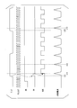
- FIG. 3 is a diagram illustrating the concept of clock signal phase adjustment in the semiconductor integrated circuit of the present invention.
- FIG. 1 is a block diagram illustrating a schematic configuration of a semiconductor integrated circuit according to a first embodiment of the present invention.
- 4 is a timing chart illustrating a phase adjustment operation in the semiconductor integrated circuit according to the first embodiment of the present invention.
- FIG. 9 is a block diagram illustrating a schematic configuration of a semiconductor integrated circuit according to a second embodiment of the present invention.
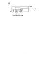
- FIG. 9 is a block diagram illustrating an example of a schematic configuration of a delay adjustment unit provided in a semiconductor integrated circuit according to a second embodiment of the present invention.
- 9 is a timing chart illustrating a phase adjustment operation in the semiconductor integrated circuit according to the second embodiment of the present invention.
- FIG. 1 is a block diagram illustrating a schematic configuration of a semiconductor integrated circuit according to a first embodiment of the present invention.
- 4 is a timing chart illustrating a phase adjustment operation in the semiconductor integrated circuit according to the first embodiment of
- FIG. 11 is a block diagram illustrating a schematic configuration of a semiconductor integrated circuit according to a third embodiment of the present invention.
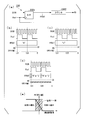
- FIG. 11 is a diagram illustrating an example of a schematic configuration of a phase comparison unit provided in a semiconductor integrated circuit according to a third embodiment of the present invention and an example of an operation of the phase comparison unit.
- FIG. 11 is a block diagram illustrating a schematic configuration of a semiconductor integrated circuit according to a fourth embodiment of the present invention.
- FIG. 14 is a block diagram illustrating an example of a schematic configuration of a delay fine adjustment unit provided in a semiconductor integrated circuit according to a fourth embodiment of the present invention.
- the timing at which the level of the output signal output from the semiconductor integrated circuit changes is shifted from the timing at which the signal waveform of the clock signal input to the semiconductor integrated circuit changes (transitions).
- the basic idea is to reduce the fluctuation (jitter) occurring in the signal waveform of each clock signal. That is, in the semiconductor integrated circuit of the present invention, the timing at which power supply noise (self-noise) that causes a power supply to fluctuate on a system board of an apparatus (system) mounting the semiconductor integrated circuit is input to the semiconductor integrated circuit.
- the basic idea is to shift from the timing at which the level of the clock signal changes (transitions).
- the phase of the clock signal used in the semiconductor integrated circuit generated based on the input clock signal is adjusted to be shifted from the phase of the clock signal input to the semiconductor integrated circuit. That is, in the semiconductor integrated circuit of the present invention, the operation timing of the circuit element operating in synchronization with the clock signal is adjusted to be shifted from the timing at which the level of the clock signal input to the semiconductor integrated circuit changes (transitions).
- FIG. 1 is a diagram for explaining the concept of phase adjustment of a clock signal in a semiconductor integrated circuit according to the present invention.
- FIG. 1 shows a clock signal (hereinafter, referred to as a “reference clock signal”) input to a semiconductor integrated circuit as a reference clock signal in an apparatus (system) equipped with the semiconductor integrated circuit of the present invention, and an output of the semiconductor integrated circuit.
- 2 shows the timing of a parallel output signal of a plurality of bits and a clock signal (hereinafter, referred to as an “internal clock signal”) generated from a reference clock signal in the semiconductor integrated circuit and used in the semiconductor integrated circuit.
- FIG. 1 shows a clock signal (hereinafter, referred to as a “reference clock signal”) input to a semiconductor integrated circuit as a reference clock signal in an apparatus (system) equipped with the semiconductor integrated circuit of the present invention, and an output of the semiconductor integrated circuit.
- an internal clock signal shows the timing of a parallel output signal of a plurality of bits and a clock signal generated from
- FIG. 1 shows the timing of power supply noise (self-noise) of a semiconductor integrated circuit that occurs with a change (transition) in the level of an output signal.
- FIG. 1A shows the timing of a transient current generated as power supply noise when the concept of phase adjustment in the semiconductor integrated circuit of the present invention is not applied.
- FIG. 1B shows the timing of a transient current generated as power supply noise when the concept of phase adjustment in the semiconductor integrated circuit of the present invention is applied.
- the semiconductor integrated circuit multiplies the reference clock signal by using the rising edge timing (time t01 or time t03) at which the level of the reference clock signal changes (transition) as a reference. Generates internal clock signal. For this reason, in a semiconductor integrated circuit to which the concept of the phase adjustment is not applied in the semiconductor integrated circuit of the present invention, as shown in FIG.
- the output signal changes at times t01, time t02, time t03, and the like.
- timing for example, time At time t01, time t02, time t03, etc.
- the timing for example, time t01, time t02
- the timing synchronized with each rising edge of the internal clock signal shown in FIG. At time t03
- a lot of power supply noise is generated.
- the reference clock signal greatly fluctuates as shown in the transition period J of the reference clock signal. That is, in a device (system) equipped with a semiconductor integrated circuit to which the concept of phase adjustment in the semiconductor integrated circuit of the present invention is not applied, jitter occurs at the rising edge of a reference clock signal used as a reference for an internal clock signal.
- the semiconductor integrated circuit causes the rising edge timing (the time t01 or the time t01) at which the level of the reference clock signal changes (transitions).
- the internal clock signal is generated by multiplying the reference clock signal with reference to time t03).
- the timing of the rising edge of the generated internal clock signal is changed to the time t11 or the time t13.
- the timing is shifted from the timing of the rising edge of the reference clock signal.
- the phase of the generated internal clock signal is shifted from the phase of the reference clock signal.
- the time is synchronized with each rising edge of the internal clock signal. At time t11, time t12, time t13, and the like, the output signal changes.
- Time t12, time t13, etc. a large amount of transient current flows. That is, in the semiconductor integrated circuit to which the concept of the phase adjustment in the semiconductor integrated circuit of the present invention is applied, similarly to the semiconductor integrated circuit to which the concept of the phase adjustment in the semiconductor integrated circuit of the present invention is not applied, each rising edge of the internal clock signal is used. At a timing synchronized with the above (for example, time t11, time t12, time t13, etc.), a large amount of power supply noise is generated.
- the level of the reference clock signal changes (In this case, power supply noise is generated during a period in which the level of the reference clock signal is stable at any level, avoiding a rising period during which the transition occurs. Therefore, in the semiconductor integrated circuit to which the concept of the phase adjustment in the semiconductor integrated circuit of the present invention is applied, the influence of the generated power supply noise on the reference clock signal is reduced.
- the timing of the rising edge of the internal clock signal generated based on the reference clock signal is changed from the timing of the rising edge of the reference clock signal.
- power supply noise self-noise
- jitter fluctuation
- FIG. 2 is a block diagram showing a schematic configuration of the semiconductor integrated circuit according to the first embodiment of the present invention.
- the semiconductor integrated circuit 1 shown in FIG. 2 includes a comparator 10, a control unit 20, a system PLL (Phase Locked Loop) 30, a clock frequency dividing circuit 31, an edge detecting circuit 310, a large-scale circuit block 32, An output buffer 33.
- the semiconductor integrated circuit 1 includes a PLL 40, a large-scale circuit block 41, a PLL 50, and an analog circuit 51. Note that each of the PLL 40, the large-scale circuit block 41, the PLL 50, and the analog circuit 51 shown in FIG. 2 uses the reference clock signal as a common source, and the reference clock signal deteriorates due to the fluctuation of the power supply noise. Is shown as an example of a circuit affected by the jitter performance.
- the semiconductor integrated circuit 1 is a large-scale semiconductor integrated circuit realized by, for example, an ASIC (Application Specialized Integrated Circuit) or the like.
- the semiconductor integrated circuit 1 realizes a predetermined function in a device (system) on which the semiconductor integrated circuit 1 is mounted.
- the semiconductor integrated circuit 1 is mounted on a system board for configuring a system of the apparatus, and based on a clock signal of a predetermined frequency output from a clock supply circuit mounted together on the same system board, the system of the apparatus.
- the operation for realizing the predetermined function in is performed.
- the clock supply circuit mounted on the system board for example, a clock oscillation circuit such as a crystal oscillator or a crystal oscillator can be considered.
- the clock supply circuit mounted on the system board of the device is a crystal oscillator
- the semiconductor integrated circuit 1 uses the clock signal oscillated by the crystal oscillator (hereinafter referred to as “original oscillation clock signal Xtal”). The description will be made assuming that the operation is performed based on.
- the comparator 10 is a clock buffer circuit that shapes the waveform of the original oscillation clock signal Xtal that is oscillated and output by the clock supply circuit (crystal oscillator) and supplies the waveform to the components included in the semiconductor integrated circuit 1.
- the comparator 10 shapes the waveform of the sine wave original oscillation clock signal Xtal into a rectangular wave, for example.
- the comparator 10 supplies the original oscillation clock signal Xtal (hereinafter, referred to as “reference clock signal RCK”) whose waveform has been shaped to each of the system PLL 30, the edge detection circuit 310, the PLL 40, and the PLL 50.
- the control unit 20 is a control unit that controls execution of phase adjustment for a clock signal for operating each component included in the semiconductor integrated circuit 1.
- the control unit 20 outputs a phase adjustment enable signal EN to the edge detection circuit 310 when adjusting the phase of the clock signal.
- the control unit 20 is also a control unit that controls all functions provided in the semiconductor integrated circuit 1 in order to realize predetermined functions in the device system.
- the control unit 20 is a processing device such as a CPU (Central Processing Unit), for example.
- the control unit 20 controls all functions provided in the semiconductor integrated circuit 1 according to a program or data for controlling each component provided in the semiconductor integrated circuit 1.
- the control unit 20 may be provided in the system of the apparatus and control other components mounted on the same system board.
- a program and data for the control unit 20 to control each function included in the semiconductor integrated circuit 1 and each component included in the system of the device are stored in a storage device (not illustrated) such as a memory, for example. It may be something.
- control unit 20 reads out and executes the programs and data stored in the memory, and controls the entire functions of the semiconductor integrated circuit 1 and the entire components included in the system of the device. I do.
- the control unit 20 is not limited to the configuration provided in the semiconductor integrated circuit 1, but may be provided outside the semiconductor integrated circuit 1, that is, mounted on the same system board.
- the system PLL 30 is a phase synchronous circuit that generates a synchronous clock signal PLLOUT synchronized with the reference clock signal RCK output from the comparator 10.
- the system PLL 30 generates a synchronous clock signal PLLOUT obtained by multiplying the reference clock signal RCK by an integral multiple, that is, a synchronous clock signal PLLOUT having a higher frequency than the frequency of the reference clock signal RCK. Then, the system PLL 30 outputs the generated synchronous clock signal PLLOUT to the clock frequency dividing circuit 31 and the edge detecting circuit 310.
- the edge detection circuit 310 detects a rising edge of the reference clock signal RCK output from the comparator 10 under the control of the control unit 20.
- the edge detection circuit 310 outputs a signal indicating the timing at which the rising edge of the reference clock signal RCK is detected to the clock frequency division circuit 31. More specifically, when the phase adjustment enable signal EN is output from the control unit 20, the edge detection circuit 310 detects the first rising edge of the reference clock signal RCK at the timing of the rising edge of the synchronous clock signal PLLOUT. . Then, the edge detection circuit 310 resets the signal indicating the timing at which the rising edge of the reference clock signal RCK is detected, in synchronization with the rising edge of the reference clock signal RCK. Is output to the clock frequency dividing circuit 31.
- the clock dividing circuit 31 divides the frequency of the synchronous clock signal PLLOUT output from the system PLL 30 and generates an internal clock signal ICK for operating each circuit element in the corresponding large-scale circuit block 32. Circuit.
- the clock dividing circuit 31 generates an internal clock signal ICK obtained by dividing the synchronous clock signal PLLOUT by a predetermined dividing ratio. Then, the clock dividing circuit 31 outputs the generated internal clock signal ICK to each circuit element in the large-scale circuit block 32.
- the operation of dividing the frequency of the synchronous clock signal PLLOUT in the clock frequency dividing circuit 31 is reset by the synchronous reset signal SR output from the edge detecting circuit 310.
- the clock frequency dividing circuit 31 starts generating the internal clock signal ICK from the timing when the synchronous reset signal SR is released. Therefore, the internal clock signal ICK generated by the clock frequency dividing circuit 31 is the first of the reference clock signals RCK detected by the edge detection circuit 310 after the control unit 20 outputs the phase adjustment enable signal EN to the edge detection circuit 310. Becomes a clock signal synchronized with the timing of the rising edge of.
- the large-scale circuit block 32 is a digital circuit element group that realizes a predetermined function in the semiconductor integrated circuit 1 at a timing based on the clock of the internal clock signal ICK output from the clock frequency dividing circuit 31. Each circuit element provided in the large-scale circuit block 32 realizes a predetermined function at a timing synchronized with the internal clock signal ICK. Then, the large-scale circuit block 32 outputs to the output buffer 33 a signal indicating a result of realizing a predetermined function at a timing synchronized with the internal clock signal ICK.
- FIG. 2 shows a configuration in which the large-scale circuit block 32 outputs to the output buffer 33 a multi-bit parallel signal representing a result of realizing a predetermined function.
- the output buffer 33 is a buffer circuit that outputs a signal indicating a result of the large-scale circuit block 32 realizing a predetermined function as an output signal OUT in the semiconductor integrated circuit 1 to the outside of the semiconductor integrated circuit 1.
- the large-scale circuit block 32 outputs, to the output buffer 33, a multi-bit parallel signal representing a result of realizing a predetermined function at a timing synchronized with the internal clock signal ICK. Therefore, the output buffer 33 also outputs a parallel output signal OUT of a plurality of bits to the outside of the semiconductor integrated circuit 1.
- the PLL 40 is a phase synchronization circuit that generates a PLL clock signal synchronized with the reference clock signal RCK output from the comparator 10, as in the system PLL 30. However, the PLL 40 outputs the generated PLL clock signal to the large-scale circuit block 41. That is, the PLL 40 is a phase synchronization circuit corresponding to a clock path different from that of the system PLL 30.
- the large-scale circuit block 41 is a digital circuit element group that realizes a predetermined function in the semiconductor integrated circuit 1 at a clock signal timing based on the PLL clock signal output from the PLL 40.
- Each circuit element provided in the large-scale circuit block 41 realizes a predetermined function at a timing synchronized with the PLL clock signal output from the PLL 40.
- the semiconductor integrated circuit 1 may be configured to output the result of the large-scale circuit block 41 realizing a predetermined function as an output signal to the outside of the semiconductor integrated circuit 1 as in the case of the large-scale circuit block 32. Conceivable.
- the large-scale circuit block 41 outputs a signal representing a result of realizing a predetermined function to a corresponding output buffer (not shown).
- an output signal indicating a result of the large-scale circuit block 41 realizing a predetermined function is output from an output buffer (not shown).
- the clock signal for operating the circuit elements provided in the large-scale circuit block 41 that is, the clock signal based on the PLL clock signal output from the PLL 40, is also used as the synchronous clock signal PLLOUT output from the system PLL 30.
- the internal clock signal ICK based on the above, a component for adjusting the phase may be provided.
- the semiconductor integrated circuit 1 may include a component that performs the same operation as the edge detection circuit 310 and the clock frequency dividing circuit 31 in order to generate a clock signal based on the PLL clock signal output from the PLL 40.
- power supply noise self-noise
- transition in the level of the output signal output at the timing of the clock signal based on the PLL clock signal output from the PLL 40 is also reduced by the clock supply circuit (crystal). This does not cause jitter on the rising edge of the original oscillation clock signal Xtal oscillated by the oscillator or the reference clock signal RCK output by the comparator 10.
- the PLL 50 is a phase synchronization circuit that generates a PLL clock signal synchronized with the reference clock signal RCK output from the comparator 10, as in the system PLL 30. However, the PLL 50 outputs the generated PLL clock signal to the analog circuit 51. That is, the PLL 50 is a phase synchronization circuit corresponding to a clock path different from that of the system PLL 30 or the PLL 40.
- the analog circuit 51 is an analog circuit element group that realizes a predetermined function in the semiconductor integrated circuit 1 at a timing of a clock signal based on the PLL clock signal output from the PLL 50.
- Each circuit element included in the analog circuit 51 realizes a predetermined function at a timing synchronized with the PLL clock signal output from the PLL 50.
- a path (signal line) for outputting a result of realization of a predetermined function by the analog circuit 51 is omitted, similarly to the clock path of the large-scale circuit block 41, for ease of description.
- the semiconductor integrated circuit 1 outputs the result of the analog circuit 51 realizing a predetermined function as an output signal to the outside of the semiconductor integrated circuit 1 similarly to the large-scale circuit block 32 or the large-scale circuit block 41.
- the analog circuit 51 outputs a signal representing a result of realizing a predetermined function to a corresponding output buffer (not shown).
- an output signal indicating a result of the analog circuit 51 realizing a predetermined function is output from an output buffer (not shown).
- the change (transition) of the level of the output signal output from the output buffer (not shown) corresponding to the analog circuit 51 to the outside of the semiconductor integrated circuit 1 also depends on the power supply noise (self-noise) generated in the semiconductor integrated circuit 1.
- the clock signal for operating the circuit elements included in the analog circuit 51 that is, the clock signal based on the PLL clock signal output from the PLL 50 is also based on the synchronous clock signal PLLOUT output from the system PLL 30.
- a component for adjusting the phase may be provided.
- the semiconductor integrated circuit 1 may include a component that operates in the same manner as the edge detection circuit 310 and the clock frequency dividing circuit 31 in order to generate a clock signal based on the PLL clock signal output from the PLL 50.
- power supply noise self-noise
- transition in the level of the output signal output at the timing of the clock signal based on the PLL clock signal output from the PLL 50 is also reduced by the clock supply circuit (crystal). This does not cause jitter on the rising edge of the original oscillation clock signal Xtal oscillated by the oscillator or the reference clock signal RCK output by the comparator 10.
- FIG. 3 is a timing chart showing a phase adjustment operation in the semiconductor integrated circuit 1 according to the first embodiment of the present invention.
- FIG. 3 shows timings of signals output from respective components of the clock path of the internal clock signal ICK in the semiconductor integrated circuit 1. More specifically, the timings of the original oscillation clock signal Xtal, the synchronous clock signal PLLOUT, the phase adjustment enable signal EN, the synchronous reset signal SR, and the internal clock signal ICK are shown. The timing of the original oscillation clock signal Xtal shown in FIG.
- FIG. 3 is also the timing of the reference clock signal RCK at which the edge detection circuit 310 detects a rising edge. In the following description, it is assumed that the edge detection circuit 310 detects the rising edge of the original oscillation clock signal Xtal.
- FIG. 3 shows the timing of a transient current as the timing of power supply noise (self-noise) generated at a timing based on the internal clock signal ICK in the semiconductor integrated circuit 1.
- the control unit 20 when the power of the system board of the device is turned on and the control unit 20 is started, the operation of the phase adjustment is started. At this time, the control unit 20 first sets the phase adjustment enable signal EN to the “High” level. Thereby, the edge detection circuit 310 detects the rising edge of the original oscillation clock signal Xtal according to the “High” level of the phase adjustment enable signal EN.
- FIG. 3 shows an operation when the edge detection circuit 310 detects a rising edge of the original oscillation clock signal Xtal at the time t01.
- the edge detection circuit 310 Upon detecting the rising edge of the original oscillation clock signal Xtal at time t01, the edge detection circuit 310 outputs a synchronous reset signal SR for one cycle of the synchronous clock signal PLLOUT to the clock frequency dividing circuit 31. That is, the edge detection circuit 310 sets the synchronous reset signal SR to the “High” level at the time t01, and thereafter sets the synchronous reset signal SR to the “Low” level at the time t11. As a result, the clock dividing circuit 31 resets the frequency division operation by the “High” level of the synchronous reset signal SR output from the edge detection circuit 310, and the synchronous reset signal SR becomes the “Low” level.
- the internal clock signal ICK output from the clock frequency dividing circuit 31 is a clock whose phase is shifted by one cycle of the synchronous clock signal PLLOUT from the timing of the rising edge of the original oscillation clock signal Xtal detected by the edge detecting circuit 310.
- the internal clock signal ICK shown in FIG. 3 is an example when the frequency of the synchronous clock signal PLLOUT is divided by 5. That is, the frequency of the internal clock signal ICK shown in FIG. 3 is 1/5 times the frequency of the synchronous clock signal PLLOUT.
- the signal output from the output buffer 33 by the large-scale circuit block 32 performing a predetermined function also changes from the timing of the rising edge of the original oscillation clock signal Xtal to the timing of the synchronous clock signal PLLOUT.
- the signal is a signal whose level changes (transitions) when the phase is shifted by one cycle, for example, at time t11, time t12, and time t13.
- the system board of the device for example, at time t11 according to a change (transition) of the level of the output signal OUT output in synchronization with each rising edge of the internal clock signal ICK output by the semiconductor integrated circuit 1.
- Time t12, time t13, etc. many transient currents flow as shown in FIG.
- the output signal OUT output from the semiconductor integrated circuit 1 is synchronized. Power supply noise will occur.
- the power supply noise generated by the semiconductor integrated circuit 1 changes the timing of the time t01 or the time t03 during the change (transition) of the levels of the original oscillation clock signal Xtal and the reference clock signal RCK. Avoidance occurs during a period in which the level of the original oscillation clock signal Xtal or the reference clock signal RCK is stable at any level. Therefore, the power supply noise generated by the semiconductor integrated circuit 1 on the system board of the device has little effect on the original oscillation clock signal Xtal and the reference clock signal RCK, and the rising edge of the original oscillation clock signal Xtal and the reference clock signal RCK. It does not cause jitter.
- the edge detecting circuit 310 detects the rising edge of the reference clock signal RCK and resets the clock dividing circuit 31. Thereby, in the semiconductor integrated circuit 1, the timing of the rising edge of the internal clock signal ICK generated based on the reference clock signal RCK (original oscillation clock signal Xtal) is set to the rising edge of the reference clock signal RCK (original oscillation clock signal Xtal). From the timing of. Accordingly, in the semiconductor integrated circuit 1, the timing of the power supply noise (self-noise) generated on the system board of the device due to the change (transition) of the level of the output signal OUT output to the outside is determined by the reference clock signal RCK (original oscillation).
- the reference clock signal RCK original oscillation
- the semiconductor integrated circuit 1 eliminates power supply noise (self-noise) that causes fluctuation (jitter) at the rising edge of the reference clock signal RCK (original oscillation clock signal Xtal).
- a synchronous clock signal obtained by multiplying the reference clock signal RCK by synchronizing with the reference clock signal (which may be the reference clock signal RCK or the original oscillation clock signal Xtal) is used.
- An edge at which the signal waveform of the reference clock signal RCK changes at the timing of the generated phase synchronous circuit (system PLL 30) and the synchronous clock signal PLLOUT is detected, and the rising edge is detected.
- An edge detection circuit for outputting an edge detection signal (edge detection signal ED) indicating a timing, and a frequency-divided clock signal reset at a timing corresponding to the edge detection signal ED and obtained by dividing the synchronous clock signal PLLOUT (Internal clock signal ICK)
- edge detection circuit 310 for outputting an edge detection signal (edge detection signal ED) indicating a timing, and a frequency-divided clock signal reset at a timing corresponding to the edge detection signal ED and obtained by dividing the synchronous clock signal PLLOUT (Internal clock signal ICK)
- click divider circuit the clock divider circuit 31
- a semiconductor integrated circuit semiconductor integrated circuit
- the edge detection circuit 310 includes the semiconductor integrated circuit 1 that outputs the edge detection signal ED for one cycle of the synchronous clock signal PLLOUT.
- the semiconductor integrated circuit 1 further includes a control unit (control unit 20) that causes the edge detection circuit 310 to start detecting a rising edge.
- the edge detecting circuit 310 detects the rising edge of the reference clock signal RCK and resets the clock dividing circuit 31, so that the clock dividing circuit 31
- the timing of the rising edge of the generated internal clock signal ICK is shifted from the timing of the rising edge of the reference clock signal RCK (original oscillation clock signal Xtal).
- a change in the level of the output signal OUT output to the outside causes the system of the device (system) on which the semiconductor integrated circuit 1 of the first embodiment is mounted to be mounted.
- the entire system caused by power supply noise (self-noise) generated by the semiconductor integrated circuit 1 of the first embodiment Can be reduced.
- the internal clock signal ICK generated by the clock frequency dividing circuit 31 is changed by the synchronous reset signal SR output from the edge detecting circuit 310 to the reference clock signal RCK (original oscillation clock signal).
- RCK original oscillation clock signal
- a configuration has been described in which the phase of one cycle of the synchronous clock signal PLLOUT is shifted from the timing of the rising edge of Xtal).
- the semiconductor integrated circuit 1 of the first embodiment it is conceivable that there is a propagation delay in the clock path of the internal clock signal ICK. More specifically, in the semiconductor integrated circuit 1 of the first embodiment, when routing the signal line of the internal clock signal ICK output by the clock frequency dividing circuit 31 to each circuit element provided in the large-scale circuit block 32 It is conceivable that there is a propagation delay corresponding to the arrangement of each circuit element. For this reason, the semiconductor integrated circuit 1 of the first embodiment may have a configuration in which the phase of the internal clock signal ICK is adjusted to a timing corresponding to the propagation delay of the internal clock signal ICK.
- the semiconductor integrated circuit according to the second embodiment of the present invention considers that there is a propagation delay in the clock path of the internal clock signal ICK and adjusts the timing of the internal clock signal ICK to a timing corresponding to the propagation delay of the internal clock signal ICK. This is a configuration for adjusting the phase.
- FIG. 4 is a block diagram showing a schematic configuration of a semiconductor integrated circuit according to the second embodiment of the present invention.
- the configuration of the semiconductor integrated circuit of the second embodiment shown in FIG. 4 includes the same components as those of the semiconductor integrated circuit 1 of the first embodiment shown in FIG. Therefore, in the components of the semiconductor integrated circuit of the second embodiment, the same components as those of the semiconductor integrated circuit 1 of the first embodiment are denoted by the same reference numerals, and details regarding each component are provided. Detailed description is omitted.
- the semiconductor integrated circuit 2 shown in FIG. 4 includes a comparator 10, a control unit 20, a system PLL 30, a clock frequency dividing circuit 31, an edge detecting circuit 310, a delay adjusting unit 320, a large-scale circuit block 32, An output buffer 33.
- a delay adjustment unit 320 is added between the edge detection circuit 310 and the clock frequency dividing circuit 31 in the semiconductor integrated circuit 1 of the first embodiment.
- the propagation delay of the clock path of the internal clock signal ICK is schematically shown as a propagation delay 34 having a configuration in which a plurality of buffer circuits are connected in series.
- the semiconductor integrated circuit 2 includes a PLL 40, a large-scale circuit block 41, a PLL 50, and an analog circuit 51.
- the semiconductor integrated circuit 2 is also a large-scale semiconductor integrated circuit realized by, for example, an ASIC or the like, similarly to the semiconductor integrated circuit 1 of the first embodiment shown in FIG. Similarly to the semiconductor integrated circuit 1 of the first embodiment, the semiconductor integrated circuit 2 also realizes a predetermined function in a device (system) on which the semiconductor integrated circuit 2 is mounted. Similarly to the semiconductor integrated circuit 1 of the first embodiment, the semiconductor integrated circuit 2 is mounted on a system board for configuring an apparatus system, and is output from a clock supply circuit mounted on the same system board. An operation for realizing a predetermined function in the system of the device is performed based on a clock signal of a predetermined frequency.
- the clock supply circuit mounted on the system board of the device is a crystal oscillator
- the semiconductor integrated circuit 2 includes an original oscillation clock signal Xtal generated by the crystal oscillator. The description will be made assuming that the operation is performed based on.
- the system PLL 30 outputs the generated synchronous clock signal PLLOUT to the delay adjusting unit 320 in addition to the clock frequency dividing circuit 31 and the edge detecting circuit 310.
- the edge detection circuit 310 outputs a signal indicating the timing at which the rising edge of the reference clock signal RCK is detected to the delay adjustment unit 320 as an edge detection signal ED.
- the edge detection signal ED output from the edge detection circuit 310 to the delay adjustment unit 320 is the same signal as the synchronous reset signal SR in the first embodiment. That is, the edge detection circuit 310 outputs the synchronization reset signal SR to the delay adjustment unit 320 as the edge detection signal ED.
- the delay adjustment unit 320 delays the edge detection signal ED output from the edge detection circuit 310 by a predetermined time. More specifically, assuming that the period of the internal clock signal ICK is TICK and the delay time of the propagation delay 34 of the clock path is TDICK, the delay adjustment unit 320 delays the edge detection signal ED by the time of (TICK-TDICK). .
- the delay adjusting unit 320 outputs the delayed edge detection signal ED to the clock frequency dividing circuit 31 as a synchronous reset signal SR. More specifically, the delay adjustment unit 320 outputs the synchronous reset signal SR obtained by delaying the edge detection signal ED output from the edge detection circuit 310 by the unit of the period of the synchronous clock signal PLLOUT in the first embodiment.
- the signal is output to the clock frequency dividing circuit 31 as the same signal as the synchronous reset signal SR.
- the timing at which the clock frequency dividing circuit 31 is reset in response to the synchronous reset signal SR is determined by the delay time of the delay adjustment unit 320, that is, the time of (TICK-TDICK). It is slower than the clock divider 31 provided in the semiconductor integrated circuit 1 of the first embodiment.
- the delay adjustment unit 320 has a configuration in which the delay is delayed by a time corresponding to the above-mentioned (TICK-TDICK), that is, a configuration in which the synchronous reset signal SR in which the edge detection signal ED is delayed by a fixed delay time is output. It is not limited.
- the delay adjustment unit 320 may be configured to delay the edge detection signal ED and change the time to be output as the synchronization reset signal SR in accordance with the control from the control unit 20. That is, the delay adjustment unit 320 may be configured to change the phase adjustment amount of the internal clock signal ICK.
- the timing of the internal clock signal ICK is considered in consideration of the timing at which power supply noise (self-noise) which may vary depending on the arrangement position of each component on the system board of the device on which the semiconductor integrated circuit 2 is mounted.
- the amount of phase adjustment can be changed.
- the internal clock signal ICK generated by the clock frequency dividing circuit 31 is detected by the edge detecting circuit 310 after the controller 20 outputs the phase adjustment enable signal EN to the edge detecting circuit 310.
- This is a clock signal synchronized with the timing of the first rising edge of the reference clock signal RCK.
- the delay adjusting unit 320 delays the timing of the synchronous reset signal SR, the internal clock signal ICK generated by the clock frequency dividing circuit 31 is equal to the synchronous clock signal PLLOUT. This is a clock signal whose phase is shifted by a plurality of cycles.
- the level of the output signal OUT output from the output buffer 33 also changes (transitions) at a timing later by a plurality of cycles of the synchronous clock signal PLLOUT delayed by the delay adjuster 320.
- power supply noise self-noise
- a change (transition) in the level of the output signal OUT is generated by a clock supply circuit (crystal oscillator). Does not cause jitter at the rising edge of the original oscillation clock signal Xtal oscillated by the clock signal or the reference clock signal RCK output by the comparator 10.
- the level of the output signal OUT changes (transitions) at a timing that more reflects the propagation delay of the clock path of the internal clock signal ICK in the large-scale circuit block 32. Jitter that can occur at the rising edge of the clock signal Xtal or the reference clock signal RCK can be suppressed.
- the detailed description of the operation of adjusting the phase of the internal clock signal ICK in the semiconductor integrated circuit 2 will be described later.
- FIG. 5 is a block diagram illustrating an example of a schematic configuration of the delay adjustment unit 320 provided in the semiconductor integrated circuit 2 according to the second embodiment of the present invention.
- An example of the configuration of the delay adjustment unit 320 illustrated in FIG. 5 is an example of a configuration in which the time for delaying the edge detection signal ED can be changed, that is, the amount of phase adjustment of the internal clock signal ICK can be changed. is there.
- the delay adjustment unit 320 includes four D-type flip-flops (D-FF) 3201 to D-FF 3204 and a selector 3205.
- D-FF D-type flip-flops
- the D-FF 3201, the D-FF 3202, the D-FF 3203, and the D-FF 3204 are sequentially connected in this order, and the edge detection signal ED input to the delay adjustment unit 320 and the output signal of each D-type flip-flop Are connected as input signals of the selector 3205. Then, the delay adjustment unit 320 outputs the input signal selected by the selector 3205 as the synchronization reset signal SR.
- each D-type flip-flop captures and holds the input edge detection signal ED or the output signal of the preceding D-type flip-flop for each cycle of the synchronous clock signal PLLOUT.
- the selector 3205 selects and selects one of the edge detection signal ED and one of the output signals of the four D-type flip-flops, for example, under the control of the control unit 20.
- the signal is output as a synchronous reset signal SR.
- the delay adjustment unit 320 outputs the edge detection signal ED output from the edge detection circuit 310 as it is or the edge detection signal ED for one cycle of the synchronous clock signal PLLOUT under the control of the control unit 20. It is delayed by up to four cycles and output to the clock frequency dividing circuit 31 as the synchronous reset signal SR.
- the internal clock signal ICK generated by the clock frequency dividing circuit 31 is changed to the rising edge of the reference clock signal RCK (original oscillation clock signal Xtal) by the synchronous reset signal SR output from the delay adjusting unit 320. From the above timing, the phase is shifted by one to five cycles of the synchronous clock signal PLLOUT.
- FIG. 5 shows the configuration of the delay adjustment unit 320 that delays and outputs the edge detection signal ED by 0 to 4 cycles of the synchronous clock signal PLLOUT.
- the delay adjustment unit 320 may be configured to include a number of D-type flip-flops corresponding to one cycle of the reference clock signal RCK, that is, one cycle of the original oscillation clock signal Xtal.
- the delay adjustment unit 320 delays the edge detection signal ED by any timing of one cycle of the reference clock signal RCK and outputs it as the synchronous reset signal SR in accordance with the control from the control unit 20. be able to.
- the semiconductor integrated circuit 2 can appropriately change the amount of phase adjustment of the internal clock signal ICK even when mounted on various different devices.
- the configuration of the delay adjustment unit 320 may be any configuration as long as the configuration is such that the edge detection signal ED is delayed and output as the synchronous reset signal SR.
- the delay adjusting unit 320 does not change the time for delaying the edge detection signal ED, that is, when the phase adjustment amount of the internal clock signal ICK is fixed, the selector 3205 is not provided and the final The output signal of the D-type flip-flop (D-FF 3204 in FIG. 5) of the stage may be output to the clock frequency dividing circuit 31 as the synchronous reset signal SR.
- FIG. 6 is a timing chart showing a phase adjustment operation in the semiconductor integrated circuit 2 according to the second embodiment of the present invention.
- FIG. 6 shows signals output from respective components of the clock path of the internal clock signal ICK in the semiconductor integrated circuit 2 in the same manner as the phase adjustment operation in the semiconductor integrated circuit 1 of the first embodiment shown in FIG. FIG. More specifically, the timings of the original oscillation clock signal Xtal, the synchronization clock signal PLLOUT, the phase adjustment enable signal EN, the edge detection signal ED, the synchronization reset signal SR, and the internal clock signal ICK are shown.
- the timing of the original oscillation clock signal Xtal shown in FIG. 6 is also the same as the timing of the original oscillation clock signal Xtal in the semiconductor integrated circuit 1 of the first embodiment, and the reference clock at which the edge detection circuit 310 detects a rising edge. This is also the timing of the signal RCK. In the following description, it is assumed that the edge detection circuit 310 detects the rising edge of the original oscillation clock signal Xtal, as in the phase adjustment operation in the semiconductor integrated circuit 1 of the first embodiment.
- FIG. 6 shows the power supply noise (at the timing based on the internal clock signal ICK in the semiconductor integrated circuit 2) similar to the phase adjustment operation in the semiconductor integrated circuit 1 of the first embodiment shown in FIG.
- the timing of the transient current is shown as the timing of (self noise).
- the semiconductor integrated circuit 2 adjusts the phase of the internal clock signal ICK in consideration of the fact that the internal clock signal ICK generated by the clock frequency dividing circuit 31 is delayed by the propagation delay. For this reason, in FIG. 6, as the timing of the internal clock signal ICK, the internal clock signal ICK (before adjustment) when the delay adjustment unit 320 does not adjust the timing of the synchronous reset signal SR, and the delay adjustment unit 320 Both the internal clock signal ICK (after adjustment) when the timing of SR is adjusted is shown. Note that the timing of the internal clock signal ICK (after adjustment) shown in FIG. This is an example of a case where an output is made to the circuit 31. That is, FIG.
- the internal clock signal ICK shown in FIG. 6 is an example of a case where the synchronous clock signal PLLOUT is divided by 5 like the phase adjustment operation in the semiconductor integrated circuit 1 of the first embodiment shown in FIG. is there. That is, the frequency of the internal clock signal ICK shown in FIG. 6 is 1/5 times the frequency of the synchronous clock signal PLLOUT, like the phase adjustment operation in the semiconductor integrated circuit 1 of the first embodiment shown in FIG. It is.
- the semiconductor integrated circuit 2 when the power of the system board of the device is turned on and the control unit 20 is started, the semiconductor integrated circuit 2 also starts the phase adjustment operation.
- the control unit 20 first sets the phase adjustment enable signal EN to the “High” level, similarly to the semiconductor integrated circuit 1 of the first embodiment.
- the edge detection circuit 310 detects the rising edge of the original oscillation clock signal Xtal according to the “High” level of the phase adjustment enable signal EN. 6, the edge detection circuit 310 detects the rising edge of the original oscillation clock signal Xtal at time t01, similarly to the phase adjustment operation in the semiconductor integrated circuit 1 of the first embodiment shown in FIG. FIG.
- the edge detection circuit 310 When the edge detection circuit 310 detects the rising edge of the original oscillation clock signal Xtal at the time t01, the edge detection circuit 310 outputs an edge detection signal ED for one cycle of the synchronous clock signal PLLOUT to the delay adjustment unit 320. That is, the edge detection circuit 310 sets the edge detection signal ED to the “High” level at the time t01, and thereafter sets the edge detection signal ED to the “Low” level at the time t11.
- the delay adjustment unit 320 outputs the edge detection signal ED output from the edge detection circuit 310 to the clock frequency division circuit 31 as the synchronous reset signal SR without delay.
- the internal clock signal ICK generated by the clock frequency dividing circuit 31 is delayed by the propagation delay 34 and is output to each circuit element in the large-scale circuit block 32 at the timing of the internal clock signal ICK (before adjustment).
- the timing of the rising edge of the internal clock signal ICK (before adjustment) is close to the timing of the rising edge of the original oscillation clock signal Xtal.
- the timing of the rising edge of the internal clock signal ICK at time t13 is the timing of the rising edge of the original oscillation clock signal Xtal at time t03. It is close to. For this reason, power supply noise (self-noise) due to a transient current (before adjustment) flowing in synchronization with each rising edge of the internal clock signal ICK (before adjustment), which is indicated by a broken line in FIG. There is a concern that this may cause jitter at the rising edge of the original oscillation clock signal Xtal (reference clock signal RCK).
- the delay adjustment unit 320 delays the edge detection signal ED output from the edge detection circuit 310 by the unit of the cycle of the synchronization clock signal PLLOUT, and generates the synchronization reset signal SR as a clock division circuit. 31.
- the delay adjustment unit 320 delays the edge detection signal ED by two periods of the synchronous clock signal PLLOUT and outputs the delayed signal to the clock frequency dividing circuit 31 as the synchronous reset signal SR.
- the delay adjusting unit 320 sets the synchronous reset signal SR to the “High” level at the time t21, and thereafter sets the synchronous reset signal SR to the “Low” level at the time t22.
- the clock frequency dividing circuit 31 resets the frequency division operation according to the “High” level of the synchronous reset signal SR output from the delay adjustment unit 320, and the synchronous reset signal SR becomes the “Low” level. From the time t22 when the reset is released, the output of the internal clock signal ICK obtained by dividing the frequency of the synchronous clock signal PLLOUT is started. The internal clock signal ICK that the clock frequency dividing circuit 31 starts outputting from time t22 is also delayed by the propagation delay.
- the internal clock signal ICK that the clock frequency dividing circuit 31 has started to output from the time t22 is output from the time t23 delayed by the propagation delay 34 at the timing of the internal clock signal ICK (after adjustment) in the large-scale circuit block 32. Is output to each circuit element.
- the timing of the rising edge of the internal clock signal ICK (after adjustment) is far from the timing of the rising edge of the original oscillation clock signal Xtal. That is, the internal clock signal ICK (after adjustment) output from the clock frequency dividing circuit 31 is a clock signal whose phase is more appropriately shifted from the rising edge timing of the original oscillation clock signal Xtal detected by the edge detecting circuit 310. ing.
- the timing of the rising edge of the internal clock signal ICK at time t24 is the timing of the rising edge of the original oscillation clock signal Xtal at time t03. Is far from. For this reason, the power supply noise (self-noise) due to the transient current (after adjustment) that flows in synchronization with each rising edge of the internal clock signal ICK (after adjustment) shown by a solid line in FIG. It does not cause a jitter at the rising edge of the original oscillation clock signal Xtal (reference clock signal RCK).
- the timing at which the delay adjustment unit 320 resets the clock frequency division circuit 31 is delayed.
- the timing of the rising edge of the internal clock signal ICK is changed to the timing of the rising edge of the reference clock signal RCK (original oscillation clock signal Xtal). Shift from timing.
- the semiconductor integrated circuit 2 similarly to the semiconductor integrated circuit 1 of the first embodiment, power supply noise generated on the system board of the device due to a change (transition) in the level of the output signal OUT to be output to the outside.
- the timing of the self noise is shifted from the timing of the rising edge of the reference clock signal RCK (original oscillation clock signal Xtal). For this reason, even when the power supply noise (self-noise) is generated in the semiconductor integrated circuit 2 similarly to the semiconductor integrated circuit 1 of the first embodiment, the power supply noise is generated by the reference clock signal RCK (original oscillation clock signal). Xtal) does not become a factor that causes the rising edge to fluctuate (causes jitter). In other words, similarly to the semiconductor integrated circuit 1 of the first embodiment, the power supply noise (jitter) that causes a fluctuation (jitter) at the rising edge of the reference clock signal RCK (original oscillation clock signal Xtal) also in the semiconductor integrated circuit 2. Self noise).
- the semiconductor further includes a delay adjustment unit (delay adjustment unit 320) that delays the edge detection signal (edge detection signal ED) in units of the cycle of the synchronous clock signal (synchronous clock signal PLLOUT).
- delay adjustment unit 320 delay adjustment unit 320 that delays the edge detection signal (edge detection signal ED) in units of the cycle of the synchronous clock signal (synchronous clock signal PLLOUT).
- An integrated circuit semiconductor integrated circuit 2 is configured.
- the edge detection circuit (the edge detection circuit 310) starts the detection of the edge (the rising edge in the first embodiment), and outputs the edge detection signal (the edge detection signal ED).
- the semiconductor integrated circuit 2 further includes a control unit (control unit 20) for setting the delay time in the delay adjustment unit 320.
- the edge detection circuit 310 detects the rising edge of the reference clock signal RCK, as in the semiconductor integrated circuit 1 of the first embodiment.
- the delay adjusting unit 320 resets the clock frequency dividing circuit 31 by delaying the timing.
- the clock frequency dividing circuit 31 operates similarly to the semiconductor integrated circuit 1 according to the first embodiment.
- the timing of the rising edge of the generated internal clock signal ICK is shifted from the timing of the rising edge of the reference clock signal RCK (original oscillation clock signal Xtal).
- a change (transition) of the level of the output signal OUT to be output to the outside causes a change in the second embodiment.
- the timing at which the power supply noise (self-noise) occurs is determined by the reference clock signal RCK (original clock). This will deviate from the timing of the rising edge of the oscillation clock signal Xtal).
- the generated power supply noise (self-noise) is generated by the reference clock signal RCK (original oscillation). It does not become a factor that causes the rising edge of the clock signal Xtal) to fluctuate (causes jitter). That is, in the semiconductor integrated circuit 2 according to the second embodiment, similarly to the semiconductor integrated circuit 1 according to the first embodiment, the timing at which fluctuation (jitter) occurs at the rising edge of the reference clock signal RCK (original oscillation clock signal Xtal). Of power supply noise (self-noise).
- the device (system) equipped with the semiconductor integrated circuit 2 of the second embodiment also has the same configuration as the device (system) equipped with the semiconductor integrated circuit 1 of the first embodiment. It is possible to suppress a decrease in the performance of the entire system due to power supply noise (self-noise) generated by the semiconductor integrated circuit 2.
- the delay adjustment unit 320 uses the synchronous reset signal SR obtained by delaying the edge detection signal ED by a fixed delay time corresponding to the time of (TICK-TDICK).
- the configuration has been described in which the phase of the internal clock signal ICK generated by the frequency dividing circuit 31 is shifted from the timing of the rising edge of the reference clock signal RCK (original oscillation clock signal Xtal) in units of the period of the synchronous clock signal PLLOUT.
- the delay adjustment unit 320 can change the cycle of the synchronous clock signal PLLOUT that delays the edge detection signal ED in accordance with the control from the control unit 20. was also explained.
- the control unit 20 controls the shift amount between the timing of the rising edge of the reference clock signal RCK and the timing of the rising edge of the internal clock signal ICK, that is, the reference clock signal RCK.
- the delay adjustment unit 320 may change the period of the synchronous clock signal PLLOUT for delaying the edge detection signal ED based on the amount of phase shift between the clock signal and the internal clock signal ICK.
- the semiconductor integrated circuit according to the third embodiment of the present invention is configured such that, based on the amount of phase shift between the reference clock signal RCK and the internal clock signal ICK, the timing of the internal clock signal ICK in the clock path is determined in consideration of the propagation delay. This is a configuration for adjusting the phase of the clock signal ICK.
- FIG. 7 is a block diagram showing a schematic configuration of a semiconductor integrated circuit according to the third embodiment of the present invention.
- the configuration of the semiconductor integrated circuit of the third embodiment shown in FIG. 7 includes the semiconductor integrated circuit 1 of the first embodiment shown in FIG. 2 and the semiconductor integrated circuit of the second embodiment shown in FIG. 2 includes the same components. Therefore, in the components of the semiconductor integrated circuit of the third embodiment, the same components as the components of the semiconductor integrated circuit 1 of the first embodiment or the semiconductor integrated circuit 2 of the second embodiment are the same. Reference numerals are given, and detailed description of each component is omitted.
- the semiconductor integrated circuit 3 shown in FIG. 7 includes a comparator 10, a control unit 20, a system PLL 30, a clock frequency dividing circuit 31, an edge detecting circuit 310, a delay adjusting unit 320, a phase comparing unit 330, a dummy It includes a delay unit 331, a large-scale circuit block 32, and an output buffer 33.
- a phase comparison unit 330 and a dummy delay unit 331 are added to the semiconductor integrated circuit 2 of the second embodiment.
- the semiconductor integrated circuit 3 includes a PLL 40, a large-scale circuit block 41, a PLL 50, and an analog circuit 51.
- the semiconductor integrated circuit 3 is also realized by, for example, an ASIC, like the semiconductor integrated circuit 1 of the first embodiment shown in FIG. 2 and the semiconductor integrated circuit 2 of the second embodiment shown in FIG. This is a large-scale semiconductor integrated circuit. Similarly to the semiconductor integrated circuit 1 of the first embodiment and the semiconductor integrated circuit 2 of the second embodiment, the semiconductor integrated circuit 3 also realizes a predetermined function in a device (system) on which the semiconductor integrated circuit 3 is mounted. I do. Similarly to the semiconductor integrated circuit 1 of the first embodiment and the semiconductor integrated circuit 2 of the second embodiment, the semiconductor integrated circuit 3 is mounted on a system board for configuring an apparatus system, and is mounted on the same system board.
- An operation for realizing a predetermined function in the system of the device is performed based on a clock signal of a predetermined frequency output from a clock supply circuit mounted together.
- the clock supply circuit mounted on the system board of the device is a crystal oscillator
- the integrated circuit 3 is described as operating based on the original oscillation clock signal Xtal oscillated by the crystal oscillator.
- the comparator 10 supplies the source oscillation clock signal Xtal whose waveform has been shaped to the phase comparator 330 in addition to the system PLL 30, the edge detection circuit 310, the PLL 40, and the PLL 50.
- the clock dividing circuit 31 outputs the generated internal clock signal ICK to the dummy delay unit 331 in addition to the respective circuit elements in the large-scale circuit block 32.
- the control unit 20 determines the amount of phase adjustment of the internal clock signal ICK and sets it in the delay adjustment unit 320. More specifically, the control unit 20 determines the time for delaying the edge detection signal ED in the delay adjustment unit 320, that is, the number of D-type flip-flops, and sets (selects) the determined number of D-type flip-flops. Output to the delay adjustment unit 320.
- the configuration of the delay adjustment unit 320 provided in the semiconductor integrated circuit 3 is the configuration of the delay adjustment unit 320 shown in FIG.
- the delay adjustment unit 320 causes the selector 3205 to select one of the edge detection signal ED and one of the output signals of the four D-type flip-flops according to the delay adjustment signal DA output from the control unit 20. , And outputs the selected signal as a synchronous reset signal SR.
- the dummy delay unit 331 is a circuit that simulates a delay amount corresponding to a propagation delay of a clock path of the internal clock signal ICK. More specifically, when the dummy delay unit 331 routes the signal line of the internal clock signal ICK output by the clock frequency dividing circuit 31 to each circuit element provided in the large-scale circuit block 32, This is a delay circuit that simulates a propagation delay according to the arrangement. That is, the dummy delay unit 331 simulates the same delay amount as the propagation delay 34. In the configuration of the semiconductor integrated circuit 3 shown in FIG. 7, a dummy delay unit 331 having a configuration in which the same delay amount as the propagation delay 34 is simulated by a configuration in which a plurality of buffer circuits are connected in series is shown.
- the configuration in which the dummy delay unit 331 simulates the same delay amount as the propagation delay 34 is not limited to the configuration of the dummy delay unit 331 shown in FIG. Any configuration may be used as long as it is possible.
- the dummy delay unit 331 delays the internal clock signal ICK output from the clock frequency dividing circuit 31 by the same delay time as the propagation delay 34, and outputs the same to the phase comparison unit 330.
- the phase comparison unit 330 compares the phase of the reference clock signal RCK output from the comparator 10 with the phase of the internal clock signal ICK delayed by the dummy delay unit 331.
- the phase comparison unit 330 uses the reference clock signal RCK as a reference clock signal, and uses the internal clock signal ICK delayed by the dummy delay unit 331 (hereinafter, referred to as “delayed internal clock signal DICK”) as a clock signal to be compared. Are compared with each other.
- the phase comparison unit 330 outputs to the control unit 20 a phase comparison result signal PD indicating a result of comparing the phases of the reference clock signal RCK and the delayed internal clock signal DICK.
- the phase comparison result signal PD output by the phase comparison unit 330 includes information indicating whether the phase of the rising edge of the delayed internal clock signal DICK is ahead of or behind the phase of the rising edge of the reference clock signal RCK. It is included.
- the control unit 20 determines a time for delaying the edge detection signal ED by the delay adjustment unit 320 based on the phase comparison result signal PD output from the phase comparison unit 330, and according to the determined result. Then, the phase adjustment amount of the internal clock signal ICK is set in the delay adjustment unit 320. More specifically, in the semiconductor integrated circuit 3, the control unit 20 determines the number of stages of the edge detection signal ED to be delayed by the D-type flip-flop provided in the delay adjustment unit 320, and transmits information representing the determined number of stages to the delay.
- the adjustment signal DA is output to the selector 3205 provided in the delay adjustment unit 320.
- the selector 3205 provided in the delay adjustment unit 320 selects the output signal output from the D-type flip-flop of the number of stages indicated by the delay adjustment signal DA, and uses the selected signal as the synchronous reset signal SR. Output to the clock frequency dividing circuit 31.
- the phase of the internal clock signal ICK generated by the clock frequency dividing circuit 31 is changed according to the phase difference between the reference clock signal RCK and the delayed internal clock signal DICK compared by the phase comparing section 330. That is, the phase adjustment amount of the internal clock signal ICK is changed.
- the internal clock signal ICK generated by the clock dividing circuit 31 is detected by the edge detection circuit 310 after the control unit 20 outputs the phase adjustment enable signal EN to the edge detection circuit 310.
- This is a clock signal synchronized with the timing of the first rising edge of the reference clock signal RCK.
- the delay adjuster 320 delays the timing of the synchronous reset signal SR, the internal clock generated by the clock frequency dividing circuit 31
- the signal ICK is a clock signal whose phase is shifted by a plurality of cycles of the synchronous clock signal PLLOUT.
- the output signal OUT output from the output buffer 33 is equivalent to a plurality of cycles of the synchronous clock signal PLLOUT delayed by the delay adjustment unit 320.
- the level changes (transitions) only at a later timing.
- power supply noise self-noise
- the semiconductor integrated circuit 3 like the semiconductor integrated circuit 1 of the first embodiment and the semiconductor integrated circuit 2 of the second embodiment, power supply noise (self-noise) due to a change (transition) in the level of the output signal OUT.
- the semiconductor integrated circuit 3 since the level of the output signal OUT changes (transitions) at a timing corresponding to the phase difference between the reference clock signal RCK and the delayed internal clock signal DICK, the original oscillation clock signal Xtal and the reference Jitter that can occur at the rising edge of the clock signal RCK can be suppressed.
- the amount of phase adjustment of the internal clock signal ICK is different from that of the semiconductor integrated circuit 2 of the second embodiment. This is the same as the semiconductor integrated circuit 2 of the embodiment. Therefore, a detailed description of the operation of adjusting the phase of the internal clock signal ICK in the semiconductor integrated circuit 3 is omitted.
- FIG. 8 is a diagram illustrating an example of a schematic configuration of the phase comparator 330 provided in the semiconductor integrated circuit 3 according to the third embodiment of the present invention and an example of an operation of the phase comparator 330.
- FIG. 8A shows an example of the configuration of the phase comparison section 330.
- 8 (b) to 8 (d) show an example of the phase comparison operation in the phase comparison section 330 having the configuration shown in FIG. 8 (a).
- FIG. 8E shows a time (delay adjustment value) for delaying the edge detection signal ED to the delay adjustment unit 320 determined by the control unit 20 based on the phase comparison result signal PD output from the phase comparison unit 330. 1) schematically shows an example of the range.
- the reference clock signal RCK is a clock signal similar to the original oscillation clock signal Xtal, similarly to the semiconductor integrated circuit 1 of the first embodiment or the semiconductor integrated circuit 2 of the second embodiment. It is. In the following description, it is assumed that the phase comparison unit 330 compares the phase of the delayed internal clock signal DICK with the phase of the original oscillation clock signal Xtal.
- the phase comparator 330 the original oscillation clock signal Xtal is used as a reference clock signal for phase comparison, and the delayed internal clock signal DICK is used as a clock signal for phase comparison.
- the phase comparing section 330 includes a D-type flip-flop (D-FF) 3301 and a counter 3302.
- D-FF D-type flip-flop
- the delayed internal clock signal DICK is input as the data input of the D-FF 3301
- the original oscillation clock signal Xtal is input as the clock input of the D-FF 3301.
- the output signal FFOUT output from the D-FF 3301 is input to the counter 3302.
- the original oscillation clock signal Xtal is input as a clock input of the counter 3302. Then, the phase comparator 330 outputs the output signal of the counter 3302 as the phase comparison result signal PD.
- the D-FF 3301 captures and holds the level of the delayed internal clock signal DICK at the timing of the rising edge of the original oscillation clock signal Xtal.
- the counter 3302 counts the level of the output signal FFOUT output from the D-FF 3301, that is, the level of the held delayed internal clock signal DICK, at the timing of the rising edge of the original oscillation clock signal Xtal.
- the counter 3302 counts when the output signal FFOUT output from the D-FF 3301 is at a “High” level for a predetermined number of times, that is, for a period of a predetermined cycle in the original oscillation clock signal Xtal.
- the phase comparison section 330 outputs a value (count value) obtained by the counter 3302 counting a predetermined number of times as a phase comparison result signal PD. That is, the phase comparator 330 determines the number of times that the delayed internal clock signal DICK is at the “High” level, counted by the counter 3302 at the timing of the rising edge of the original oscillation clock signal Xtal, as the phase of the rising edge of the delayed internal clock signal DICK. Is output as information (phase comparison result signal PD) indicating whether the phase is advanced or delayed from the phase of the rising edge of the original oscillation clock signal Xtal.
- phase comparison operation in the phase comparison unit 330 shown in FIG. 8A will be described with reference to FIGS. 8B to 8D.
- the cycle of the original oscillation clock signal Xtal for counting the “High” level of the output signal FFOUT output from the D-FF 3301 by the counter 3302 included in the phase comparison unit 330 is a cycle that can be counted a plurality of times, The length, that is, the number of times of counting is not particularly defined.
- the counter 3302 included in the phase comparison unit 330 counts the “High” level of the output signal FFOUT output from the D-FF 3301 for a period of 32 cycles of the original oscillation clock signal Xtal. It will be described as what is done.
- the D-FF 3301 outputs “High” of the delayed internal clock signal DICK at time t31 or time t32 which is the timing of the rising edge of the original oscillation clock signal Xtal. Capture and hold levels. Then, the D-FF 3301 outputs the held “High” level output signal FFOUT to the counter 3302.
- the D-FF 3301 outputs “Low” of the delayed internal clock signal DICK at time t31 or time t32, which is the timing of the rising edge of the original oscillation clock signal Xtal. Capture and hold levels. Then, the D-FF 3301 outputs the held “Low” level output signal FFOUT to the counter 3302.
- the phase of the rising edge of the delayed internal clock signal DICK includes a case where the phase of the rising edge of the original oscillation clock signal Xtal is delayed and a case where the phase of the rising edge of the delayed internal clock signal Xtal are advanced. That is, the case where the phase of the rising edge of the delayed internal clock signal DICK matches the phase of the rising edge of the original oscillation clock signal Xtal and thus is not stable in one state will be described.
- the D-FF 3301 outputs “High” of the delayed internal clock signal DICK at time t31 or time t32, which is the timing of the rising edge of the original oscillation clock signal Xtal, as shown in FIG. The level or “Low” level is captured and held.
- the phase comparison unit 330 outputs to the control unit 20 a phase comparison result signal PD indicating a result of comparing the phases of the delayed internal clock signal DICK and the original oscillation clock signal Xtal. That is, the phase comparison unit 330 outputs to the control unit 20 the phase comparison result signal PD having a different count value according to the state of the phase of the rising edge of the original oscillation clock signal Xtal with respect to the phase of the rising edge of the delayed internal clock signal DICK. I do.
- the control unit 20 sets the time for delaying the edge detection signal ED to the delay adjustment unit 320 based on the count value represented by the phase comparison result signal PD output from the phase comparison unit 330. It is determined as the amount of phase adjustment of the internal clock signal ICK.
- phase comparison unit 330 when the level of the delayed internal clock signal DICK is at the “High” level for a predetermined period of the original oscillation clock signal Xtal.
- the configuration and operation of the phase comparison unit 330 are shown.
- the phase comparison section 330 is not limited to the phase comparison section having the configuration and operation shown in FIGS. 8A to 8D. More specifically, the phase comparison unit 330 provided in the semiconductor integrated circuit 3 compares the phase of the delayed internal clock signal DICK with the phase of the original oscillation clock signal Xtal, and determines at least the phase of the rising edge of the delayed internal clock signal DICK as a reference. Any configuration and operation may be used as long as the phase comparison result signal PD indicating whether or not the phase matches the phase of the rising edge of the clock signal RCK can be output.
- control unit 20 determines a time (delay adjustment value) for causing the delay adjustment unit 320 to delay the edge detection signal ED
- the control unit 20 determines that the count value represented by the phase comparison result signal PD output from the phase comparison unit 330 is stable when the phase of the delayed internal clock signal DICK and the original oscillation clock signal Xtal is delayed or advanced.
- a time (delay adjustment value) for delaying the edge detection signal ED by the delay adjustment unit 320 is determined within a range indicating that the edge detection signal ED is being performed.
- control unit 20 determines that the count value represented by the phase comparison result signal PD output from the phase comparison unit 330 matches the phase of the rising edge of the delayed internal clock signal DICK with the phase of the rising edge of the original oscillation clock signal Xtal.
- the number of stages of the D-type flip-flop provided in the delay adjustment unit 320 is determined within a range indicating that the delay is not performed.
- the signal PD is output.
- phase comparing section 330 compares the phase between count values 31-1. The result signal PD is output.
- the control unit 20 determines that the count value indicated by the phase comparison result signal PD output from the phase comparison unit 330 is in a state where the phase of the delayed internal clock signal DICK and the original oscillation clock signal Xtal is delayed or advanced.
- the semiconductor integrated circuit 3 similarly to the semiconductor integrated circuit 1 of the first embodiment or the semiconductor integrated circuit 2 of the second embodiment, when the power supply of the system board of the device is turned on and the control unit 20 is started. , The phase adjustment operation is started, and the phase adjustment enable signal EN is set to the “High” level.
- the phase of the delay internal clock signal DICK and the phase of the original oscillation clock signal Xtal are not necessarily the delay adjustment signal DA output to the delay adjustment section 320 in the phase adjustment operation when the control section 20 is started.
- the delay adjustment value is not necessarily in the range indicating the state of being late or being advanced.
- the phase comparison unit 330 performing the phase comparison after operating with the number of stages of the D-type flip-flop set in the delay adjustment unit 320 when the control unit 20 is activated, the phase of the rising edge of the delayed internal clock signal DICK becomes It is also conceivable that the original oscillation clock signal Xtal coincides with the phase of the rising edge.
- the control unit 20 temporarily sets the phase adjustment enable signal EN to the “Low” level, outputs the delay adjustment signal DA having a different delay adjustment value to the delay adjustment unit 320, and changes the phase adjustment enable signal EN to “High” again. "Level.
- the control unit 20 outputs the phase comparison result signal PD indicating that the phase of the rising edge of the delayed internal clock signal DICK matches the phase of the rising edge of the original oscillation clock signal Xtal from the phase comparison unit 330.
- the delay adjusting unit 320 outputs the synchronous reset signal SR in which the selector 3205 has selected the output signal output from the D-type flip-flops having different numbers of stages to the clock frequency dividing circuit 31, and the clock frequency dividing circuit 31 is different.
- the phase internal clock signal ICK is regenerated and output to each circuit element in the large-scale circuit block 32.
- the control unit 20 further outputs from the phase comparison unit 330 a phase comparison result signal PD indicating that the phase of the rising edge of the delayed internal clock signal DICK matches the phase of the rising edge of the original oscillation clock signal Xtal.
- the phase of the internal clock signal ICK generated by the clock frequency dividing circuit 31 is changed by repeating the phase adjustment operation in the same manner. That is, the control unit 20 changes the phase adjustment amount of the internal clock signal ICK generated by the clock frequency dividing circuit 31 by repeating the phase adjustment operation according to the phase comparison result signal PD output from the phase comparison unit 330. I do.
- the control unit 20 may be configured to store a final delay adjustment value obtained by changing the phase adjustment amount of the internal clock signal ICK generated by the clock frequency dividing circuit 31.
- the power consumption is reduced without turning off the power of the system board.
- the internal clock signal generated by the clock frequency dividing circuit 31 based on the stored delay adjustment value when returning from the low power consumption mode such as the standby mode or the sleep mode to the normal operation mode for stopping the operation of The amount of phase adjustment of ICK can be changed.
- the normal operation mode is faster than the control unit 20 repeats the phase adjustment operation according to the phase comparison result signal PD output from the phase comparison unit 330.
- the phase comparison unit 330 uses the phase of the rising edge of the reference clock signal RCK (original oscillation clock signal Xtal) and the internal clock signal ICK (delayed internal clock signal DICK) delayed by the dummy delay unit 331. ) Is compared with the phase of the rising edge.
- the control unit 20 delays the edge detection signal ED by the delay adjustment unit 320 based on the phase comparison result signal PD output from the phase comparison unit 330, that is, the clock dividing circuit.
- the phase adjustment amount of the internal clock signal ICK generated by the counter 31 is set in the delay adjustment unit 320. Accordingly, in the semiconductor integrated circuit 3, even when there is a propagation delay in the clock path of the internal clock signal ICK, the timing of the rising edge of the internal clock signal ICK is changed to the timing of the rising edge of the reference clock signal RCK (original oscillation clock signal Xtal). Shift from timing.
- the device is changed by the change (transition) of the level of the output signal OUT output to the outside.
- the timing of the power supply noise (self-noise) generated on the system board is shifted from the timing of the rising edge of the reference clock signal RCK (original oscillation clock signal Xtal). For this reason, even when the power supply noise (self-noise) is generated in the semiconductor integrated circuit 3 similarly to the semiconductor integrated circuit 1 of the first embodiment or the semiconductor integrated circuit 2 of the second embodiment, Does not become a factor that causes the rising edge of the reference clock signal RCK (original oscillation clock signal Xtal) to fluctuate (causes jitter).
- the semiconductor integrated circuit 3 also changes at the rising edge of the reference clock signal RCK (original oscillation clock signal Xtal) similarly to the semiconductor integrated circuit 1 of the first embodiment or the semiconductor integrated circuit 2 of the second embodiment. Power supply noise (self-noise) that causes (jitter) is eliminated.
- the propagation delay (propagation delay 34) of the path of the divided clock signal (internal clock signal ICK) is simulated, and the delay unit (which delays the internal clock signal ICK by a time corresponding to the propagation delay) ( A dummy delay unit 331), a phase comparison unit that compares the phases of a reference clock signal (which may be the reference clock signal RCK and the original oscillation clock signal Xtal) and the internal clock signal ICK delayed by the dummy delay unit 331. (Phase comparing section 330), and a semiconductor integrated circuit (semiconductor integrated circuit 3) is further provided.
- the delay adjustment unit sets the time corresponding to the period of the synchronization clock signal (synchronization clock signal PLLOUT) set based on the phase comparison result of the phase comparison unit 330.
- the semiconductor integrated circuit 3 configured to delay the edge detection signal (edge detection signal ED) is configured.
- the edge detection circuit (edge detection circuit 310) starts detecting an edge (a rising edge in the first embodiment), and based on the phase comparison result of the phase comparison unit 330.
- the semiconductor integrated circuit 3 further includes a control unit (control unit 20) for setting the time for delaying the edge detection signal ED in the delay adjustment unit 320.
- the edge detection circuit 310 detects the rising edge of the reference clock signal RCK, as in the semiconductor integrated circuits of the first and second embodiments. I do. Further, in the semiconductor integrated circuit 3 of the third embodiment, similarly to the semiconductor integrated circuit 2 of the second embodiment, the delay adjusting section 320 resets the clock frequency dividing circuit 31 by delaying the timing. At this time, in the semiconductor integrated circuit 3 according to the third embodiment, the control unit 20 controls the phase comparison unit 330 to determine the phase of the rising edge of the reference clock signal RCK and the internal clock signal ICK (delayed by the dummy delay unit 331).
- a time for delaying the timing at which the delay adjusting unit 320 resets the clock frequency dividing circuit 31 is set in the delay adjusting unit 320.
- the semiconductor integrated circuit 3 of the third embodiment similarly to the semiconductor integrated circuits of the first and second embodiments, a change (transition) in the level of the output signal OUT output to the outside causes Even when power supply noise (self-noise) is generated on a system board of a device (system) on which the semiconductor integrated circuit 3 of the third embodiment is mounted, the timing at which the power-supply noise (self-noise) is generated is based on a reference. This will deviate from the timing of the rising edge of the clock signal RCK (original oscillation clock signal Xtal).
- the generated power noise (self-noise) is reduced by the reference clock.
- the device (system) equipped with the semiconductor integrated circuit 3 of the third embodiment also has the same configuration as the device (system) equipped with the semiconductor integrated circuit of the first or second embodiment. It is possible to suppress a decrease in the performance of the entire system due to power supply noise (self-noise) generated by the semiconductor integrated circuit 3 of the third embodiment.
- the control unit 20 repeats the phase adjustment operation according to the phase comparison result signal PD output from the phase comparison unit 330, so that the clock frequency dividing circuit 31
- the configuration has been described in which the amount of phase adjustment of the generated internal clock signal ICK is sequentially changed.
- This is a configuration in which the phase comparison unit 330 outputs a phase comparison result signal PD indicating whether the phase of the rising edge of the delayed internal clock signal DICK is ahead or behind the phase of the rising edge of the reference clock signal RCK. It is due to something.
- the phase comparison unit 330 provided in the semiconductor integrated circuit 3 can compare the phase of the delayed internal clock signal DICK and the phase of the original oscillation clock signal Xtal with any configuration and operation. It may be.
- the phase comparator 330 included in the semiconductor integrated circuit 3 compares, for example, the phase of the rising edge of the delayed internal clock signal DICK with the phase of the rising edge of the reference clock signal RCK, and determines the magnitude of the phase shift amount.
- the configuration may be such that the phase comparison result signal PD including the information to be displayed is output.
- the control unit 20 causes the delay adjustment unit 320 to delay the edge detection signal ED based on one phase comparison result signal PD output from the phase comparison unit 330 without repeating the phase adjustment operation. The time can be determined immediately.
- the control unit 20 performs an operation of setting the phase adjustment amount of the internal clock signal ICK generated by the clock frequency dividing circuit 31 to the delay adjustment unit 320 only once according to the determined result. Is also good.
- the delay adjustment unit 320 uses the synchronous reset signal SR in which the edge detection signal ED is delayed in units of the cycle of the synchronous clock signal PLLOUT to generate a clock component.
- a configuration has been described in which the timing of the rising edge of the internal clock signal ICK generated by the peripheral circuit 31 is shifted from the timing of the rising edge of the reference clock signal RCK (original oscillation clock signal Xtal) in units of the period of the synchronous clock signal PLLOUT.
- the delay amount of the propagation delay (propagation delay 34) of the clock path of the internal clock signal ICK is not necessarily in units of the period of the synchronous clock signal PLLOUT.
- the delay time of the internal clock signal ICK input to each circuit element provided in the large-scale circuit block 32 is equal to the delay time of the synchronous clock signal PLLOUT. It is also possible that this is the time between cycles. Even in this case, in the semiconductor integrated circuits of the second and third embodiments, the phase of the internal clock signal ICK generated by the clock frequency dividing circuit 31 is shifted by the unit of the cycle of the synchronous clock signal PLLOUT. Therefore, the generated power supply noise (self-noise) does not become a factor that causes the rising edge of the reference clock signal RCK (original oscillation clock signal Xtal) to fluctuate (causes jitter).
- RCK original oscillation clock signal Xtal
- the timing of the rising edge of the internal clock signal ICK generated by the clock frequency dividing circuit 31 is set to the rising edge of the reference clock signal RCK (original oscillation clock signal Xtal).
- the amount of phase adjustment of the internal clock signal ICK is not limited to the unit of the cycle of the synchronous clock signal PLLOUT.
- the timing of the rising edge of the internal clock signal ICK generated by the clock frequency dividing circuit 31 is adjusted to the propagation delay of the internal clock signal ICK in the clock path. Thus, the timing may be shifted from the timing of the rising edge of the reference clock signal RCK (original oscillation clock signal Xtal).
- the semiconductor integrated circuit according to the fourth embodiment of the present invention considers that the clock path of the internal clock signal ICK has a propagation delay of time that is not a unit of the cycle of the synchronous clock signal PLLOUT, and In this configuration, the phase of the internal clock signal ICK is adjusted at a timing according to the propagation delay.
- FIG. 9 is a block diagram showing a schematic configuration of a semiconductor integrated circuit according to the fourth embodiment of the present invention.
- the configuration of the semiconductor integrated circuit of the fourth embodiment shown in FIG. 9 includes the semiconductor integrated circuit 1 of the first embodiment shown in FIG. 2 and the semiconductor integrated circuit of the second embodiment shown in FIG. 2. It includes the same components as the semiconductor integrated circuit 3 of the third embodiment shown in FIG. Therefore, the components of the semiconductor integrated circuit of the fourth embodiment include the semiconductor integrated circuit 1 of the first embodiment, the semiconductor integrated circuit 2 of the second embodiment, and the semiconductor integrated circuit 3 of the third embodiment.
- the same reference numerals are given to the same components as the components, and the detailed description of each component is omitted.
- the semiconductor integrated circuit 4 shown in FIG. 9 includes a comparator 10, a control unit 20, a system PLL 30, a clock frequency dividing circuit 31, an edge detecting circuit 310, a delay adjusting unit 320, a phase comparing unit 330, a dummy It includes a delay unit 331, a delay fine adjustment unit 340, a large-scale circuit block 32, and an output buffer 33.
- a fine delay adjustment unit 340 is added to the semiconductor integrated circuit 3 of the third embodiment.
- the configuration of the semiconductor integrated circuit 4 shown in FIG. 9 is the same as that of the semiconductor integrated circuit 2 of the second embodiment shown in FIG. 4 and the semiconductor integrated circuit 3 of the third embodiment shown in FIG. ,
- the propagation delay of the clock path of the internal clock signal ICK is schematically shown by a propagation delay.
- the semiconductor integrated circuit 4 includes a PLL 40, a large-scale circuit block 41, a PLL 50, and an analog circuit 51.
- the semiconductor integrated circuit 4 also includes the semiconductor integrated circuit 1 of the first embodiment shown in FIG. 2, the semiconductor integrated circuit 2 of the second embodiment shown in FIG. 4, and the semiconductor integrated circuit 2 of the third embodiment shown in FIG.
- the semiconductor integrated circuit is a large-scale semiconductor integrated circuit realized by, for example, an ASIC.
- the semiconductor integrated circuit 4 also has the semiconductor integrated circuit 4 mounted thereon, similarly to the semiconductor integrated circuit 1 of the first embodiment, the semiconductor integrated circuit 2 of the second embodiment, and the semiconductor integrated circuit 3 of the third embodiment.
- a predetermined function is realized in the device (system).
- the semiconductor integrated circuit 4 constitutes an apparatus system.
- the device Based on a clock signal of a predetermined frequency output from a clock supply circuit mounted on the same system board, the device performs an operation for realizing a predetermined function in the system of the device. .
- the semiconductor integrated circuit 1 is mounted on a system board of an apparatus.
- the clock supply circuit is a crystal oscillator, and the semiconductor integrated circuit 4 operates based on the original oscillation clock signal Xtal oscillated by the crystal oscillator.
- the internal clock signal ICK generated by the clock frequency dividing circuit 31 is output to the delay fine adjustment unit 340, and the internal clock signal ICKD output by the delay fine adjustment unit 340 is output to the large scale circuit block 32. Output to the circuit element.
- the internal clock signal ICK input to the dummy delay unit 331 replaces the internal clock signal ICKD output by the fine delay adjustment unit 340. That is, the internal clock signal ICK output to each component in the semiconductor integrated circuit 3 of the third embodiment is replaced by the internal clock signal ICKD output by the delay fine adjustment unit 340 in the semiconductor integrated circuit 4. .
- the delay fine adjustment unit 340 delays the internal clock signal ICK output from the clock frequency dividing circuit 31 by a time within one cycle of the synchronous clock signal PLLOUT, under the control of the control unit 20. That is, the delay fine adjustment unit 340 finely adjusts the timing of the rising edge of the internal clock signal ICK to match the propagation delay 34 in the clock path of the internal clock signal ICK.
- the delay fine adjustment unit 340 outputs the delayed internal clock signal ICK to each circuit element in the large-scale circuit block 32 and the dummy delay unit 331 as the internal clock signal ICKD.
- FIG. 10 is a block diagram illustrating an example of a schematic configuration of the delay fine adjustment section 340 provided in the semiconductor integrated circuit 4 according to the fourth embodiment of the present invention.
- the delay fine adjustment unit 340 includes four buffer circuits 3401 to 3404 and a selector 3405.
- the buffer circuit 3401, the buffer circuit 3402, the buffer circuit 3403, and the buffer circuit 3404 are sequentially connected in this order, and the internal clock signal ICK input to the fine delay adjustment section 340 and the output signal of each buffer circuit are provided.
- the selector 3405 Are connected as input signals of the selector 3405.
- delay fine adjustment section 340 outputs the input signal selected by selector 3405 as internal clock signal ICKD.
- each buffer circuit delays the input internal clock signal ICK or the output signal of the preceding buffer circuit by the delay time of the element in the buffer circuit, and outputs the delayed signal.
- the selector 3405 selects one of the internal clock signal ICK and one of the output signals of the four buffer circuits according to the control from the control section 20, and converts the selected signal to the internal signal. Output as the clock signal ICKD.
- the delay fine adjustment unit 340 converts the internal clock signal ICK output from the clock frequency dividing circuit 31 as it is or converts the internal clock signal ICK into one buffer circuit in accordance with the control from the control unit 20. It is delayed by up to four and output as an internal clock signal ICKD to each circuit element in the large-scale circuit block 32.
- the internal clock signal ICKD in which each circuit element in the large-scale circuit block 32 operates is changed by one cycle of the synchronous clock signal PLLOUT, as in the semiconductor integrated circuit 3 of the third embodiment. In this configuration, the phases of up to five cycles are shifted, and the phases of one to four buffer circuits are further shifted.
- FIG. 10 shows the configuration of delay fine-adjustment unit 340 that outputs internal clock signal ICK as it is or by delaying one to four buffer circuits, but the configuration of delay fine-adjustment unit 340 Is not limited to the configuration shown in FIG.
- the delay fine adjustment unit 340 may be configured to include a number of buffer circuits capable of setting a delay time for one cycle of the synchronous clock signal PLLOUT.
- the delay fine adjustment unit 340 delays the internal clock signal ICK to any timing of one cycle of the synchronous clock signal PLLOUT according to the control from the control unit 20, and generates the internal clock signal ICKD as the internal clock signal ICKD. Can be output.
- the phase adjustment amount of the internal clock signal ICKD can be appropriately changed even when the semiconductor integrated circuit 2 is mounted on various different devices.
- the configuration of delay fine adjustment section 340 may be any configuration as long as internal clock signal ICK is delayed and output as internal clock signal ICKD.
- the delay fine adjustment unit 340 does not have to change the time for delaying the internal clock signal ICK, that is, may have a configuration in which the amount of phase adjustment of the internal clock signal ICK is fixed.
- the delay fine adjustment unit 340 does not include the selector 3405, and uses the output signal of the final-stage buffer circuit (the buffer circuit 3404 in FIG. 10) as the internal clock signal ICKD in each circuit in the large-scale circuit block 32. It is configured to output to the element and the dummy delay unit 331.
- the dummy delay unit 331 delays the internal clock signal ICKD output from the fine delay adjustment unit 340 by the same delay time as the propagation delay 34, and outputs the delayed internal clock signal DICK to the phase comparison unit 330 as a delayed internal clock signal DICK.
- the control unit 20 finely adjusts the phase of the internal clock signal ICK based on the same concept as the phase adjustment of the internal clock signal ICK in the semiconductor integrated circuit 3 of the third embodiment. Then, the delay time of the internal clock signal ICK is determined by the delay fine adjustment unit 340, and the phase adjustment amount of the internal clock signal ICK is set in the delay fine adjustment unit 340 according to the determined result. At this time, a signal for the control unit 20 to set the phase adjustment amount of the internal clock signal ICK to the delay fine adjustment unit 340 is determined by the control unit 20 May be the same as the delay adjustment signal DA for setting. In the semiconductor integrated circuit 4 shown in FIG.
- a configuration is shown in which the control unit 20 also outputs the delay adjustment signal DA to the fine delay adjustment unit 340. That is, a configuration is shown in which the control unit 20 sets the time for delaying the signal corresponding to each of the delay adjustment unit 320 and the delay fine adjustment unit 340 by the delay adjustment signal DA.
- the control unit 20 determines the number of stages of the internal clock signal ICK to be delayed by the buffer circuit provided in the delay fine adjustment unit 340, and uses information representing the determined number of stages as the delay adjustment signal DA.
- the signal is output to the selector 3405 provided in the delay fine adjustment unit 340.
- the selector 3405 provided in the delay fine adjustment unit 340 selects the output signals output from the buffer circuits of the number of stages indicated by the delay adjustment signal DA, and uses the selected signal as the internal clock signal ICKD. It outputs to each circuit element in the scale circuit block 32 and the dummy delay unit 331.
- the clock frequency dividing circuit 31 operates according to the phase difference between the reference clock signal RCK compared by the phase comparing unit 330 and the delayed internal clock signal DICK including the delay time by the delay fine adjusting unit 340.
- the phase of the generated internal clock signal ICK is changed, that is, the phase adjustment amount of the internal clock signal ICK before being delayed by the delay fine adjustment unit 340 is changed.
- the output signal OUT output from the output buffer 33 is set within one cycle of the synchronous clock signal PLLOUT delayed by the delay fine adjustment unit 340, as compared with the semiconductor integrated circuit 3 of the third embodiment.
- the level changes (transitions) at a timing later by the time of.
- the output signal OUT is output.
- Power supply noise due to a level change (transition) causes jitter on the rising edge of the original oscillation clock signal Xtal oscillated by the clock supply circuit (crystal oscillator) or the reference clock signal RCK output by the comparator 10. It is not a factor. Rather, in the semiconductor integrated circuit 4, the level of the output signal OUT changes (transitions) at a timing corresponding to the phase difference between the reference clock signal RCK and the delay internal clock signal DICK including the delay time by the delay fine adjustment unit 340. Jitter that can occur at the rising edge of the original oscillation clock signal Xtal or the reference clock signal RCK can be more appropriately suppressed than the semiconductor integrated circuit 3 of the third embodiment.
- the amount of phase adjustment of the internal clock signal ICK is different from that of the semiconductor integrated circuit 2 of the second embodiment or the semiconductor integrated circuit 3 of the third embodiment.
- the operation of adjusting the phase of the ICK is the same as that of the semiconductor integrated circuit 2 of the second embodiment or the semiconductor integrated circuit 3 of the third embodiment. Therefore, a detailed description of the operation of adjusting the phase of the internal clock signal ICK in the semiconductor integrated circuit 4 is omitted.
- the delay fine adjustment unit 340 delays the internal clock signal ICK generated by the clock frequency dividing circuit 31 by a time within one cycle of the synchronous clock signal PLLOUT.
- the phase comparator 330 determines the phase of the rising edge of the reference clock signal RCK (original oscillation clock signal Xtal) and the dummy delay unit 331. Is compared with the phase of the rising edge of the delayed internal clock signal ICK (delayed internal clock signal DICK including the delay time by the delay fine adjustment unit 340).
- the control unit 20 controls the delay adjustment unit 320 to delay the edge detection signal ED and the delay fine adjustment unit 340.
- the time for delaying the internal clock signal ICK that is, the phase adjustment amount of the internal clock signal ICK generated by the clock frequency dividing circuit 31 is set for each of the delay adjustment unit 320 and the delay fine adjustment unit 340.
- the semiconductor integrated circuit 4 also outputs to the outside similarly to the semiconductor integrated circuit 1 of the first embodiment, the semiconductor integrated circuit 2 of the second embodiment, and the semiconductor integrated circuit 3 of the third embodiment.
- the timing of the power supply noise (self-noise) generated on the system board of the device due to the change (transition) of the level of the output signal OUT is shifted from the timing of the rising edge of the reference clock signal RCK (original oscillation clock signal Xtal).
- the power supply noise (self- Noise)
- this power supply noise does not become a factor that causes the rising edge of the reference clock signal RCK (original oscillation clock signal Xtal) to fluctuate (causes jitter).
- the semiconductor integrated circuit 4 also has the same reference clock signal RCK as the semiconductor integrated circuit 1 of the first embodiment, the semiconductor integrated circuit 2 of the second embodiment, and the semiconductor integrated circuit 3 of the third embodiment. Power supply noise (self-noise) that causes fluctuation (jitter) at the rising edge of the (original oscillation clock signal Xtal) is eliminated.
- a fine delay adjuster for delaying the divided clock signal (internal clock signal ICK) by a time within one cycle of the synchronous clock signal (synchronous clock signal PLLOUT),
- the delay unit (dummy delay unit 331) further delays the internal clock signal ICK delayed by the delay fine adjustment unit 340 by a time corresponding to the propagation delay (propagation delay 34).
- the circuit 4) is configured.
- the delay fine adjustment unit 340 delays the internal clock signal ICK by a time set based on the phase comparison result of the phase comparison unit (phase comparison unit 330).
- the circuit 4 is configured.
- the edge detection circuit (edge detection circuit 310) starts detecting an edge (a rising edge in the first embodiment), and based on the phase comparison result of the phase comparison unit 330.
- a control unit (control unit) that sets a time for delaying the edge detection signal (edge detection signal ED) in the delay adjustment unit (delay adjustment unit 320) and sets a time for delaying the internal clock signal ICK in the delay fine adjustment unit 340
- the semiconductor integrated circuit 4 further includes a unit 20).
- the edge detection circuit 310 detects the rising edge of the reference clock signal RCK, as in the semiconductor integrated circuits of the first to third embodiments.
- the delay adjusting unit 320 delays the timing and resets the clock frequency dividing circuit 31.
- the control unit 20 controls the phase comparison unit 330 to determine the phase of the rising edge of the reference clock signal RCK and the internal clock signal ICK (delayed by the dummy delay unit 331).
- Time to delay the timing at which the delay adjusting unit 320 resets the clock frequency dividing circuit 31 based on the phase comparison result signal PD obtained by comparing the phase of the rising edge of the delayed internal clock signal DICK including the delay time by the fine adjusting unit 340 Is set in the delay adjustment unit 320. Further, in the semiconductor integrated circuit 4 of the fourth embodiment, the control unit 20 delays the internal clock signal ICK generated by the clock frequency dividing circuit 31 by the delay fine adjustment unit 340, within one cycle of the synchronous clock signal PLLOUT. The time is set in the delay fine adjustment unit 340.
- the clock divider circuit can be used similarly to the semiconductor integrated circuits according to the first to third embodiments.
- the timing of the rising edge of the internal clock signal ICK generated by 31 is shifted from the timing of the rising edge of the reference clock signal RCK (original oscillation clock signal Xtal).
- RCK original oscillation clock signal Xtal
- the timing at which the power supply noise (self-noise) occurs is determined by the reference clock signal RCK.
- RCK (Original oscillation clock signal Xtal) is shifted from the rising edge timing.
- the generated power supply noise (self-noise) causes the reference clock signal RCK ( It does not become a factor that causes the rising edge of the original oscillation clock signal Xtal) to fluctuate (causes jitter).
- a fluctuation occurs at the rising edge of the reference clock signal RCK (original oscillation clock signal Xtal). Eliminates the occurrence of power supply noise (self-noise) at the timing when it occurs.
- the fourth embodiment It is possible to suppress a decrease in performance of the entire system due to power supply noise (self-noise) generated by the semiconductor integrated circuit 4 of the embodiment.
- the control unit 20 controls the phase according to the phase comparison result signal PD output from the phase comparison unit 330.
- the phase comparison unit 330 outputs the phase information including the information indicating the magnitude of the phase shift amount.
- the configuration may be such that the comparison result signal PD is output, and the control unit 20 may not repeat the operation of the phase adjustment.
- the control unit 20 outputs the one-time phase comparison result signal PD output from the phase comparison unit 330.
- each of the delay adjustment unit 320 and the delay fine adjustment unit 340 may perform an operation of setting the phase adjustment amount of the internal clock signal ICK generated by the clock frequency dividing circuit 31 only once.
- the control unit 20 controls the phase adjustment amount of the internal clock signal ICK generated by the clock frequency dividing circuit 31.
- a configuration in which the changed final delay adjustment value is stored may be used.
- the control unit 20 changes the phase adjustment amount of the internal clock signal ICK generated by the clock frequency dividing circuit 31 using the previous delay adjustment value. can do.
- a rising edge of a reference clock signal (original oscillation clock signal) is detected in a semiconductor integrated circuit, and an internal clock signal is detected at the timing of the detected reference clock signal.
- an edge detection circuit for resetting a clock frequency dividing circuit that generates the clock signal.
- the timing at which the level of the output signal output from the semiconductor integrated circuit to the outside changes is shifted from the timing of the rising edge of the reference clock signal.
- power supply noise generated on a system board of a device (system) equipped with a semiconductor integrated circuit due to a change (transition) in the level of an output signal output from the semiconductor integrated circuit to the outside. (Self-noise) does not become a factor that causes the rising edge of the reference clock signal to fluctuate (causes jitter).
- the edge detection circuit is provided in the semiconductor integrated circuit in units of the cycle of the original clock signal (PLL clock signal) of the internal clock signal generated by dividing the frequency by the clock divider circuit.
- the control unit sets the time for delaying the timing at which the delay adjusting unit resets the clock frequency dividing circuit. Accordingly, in each of the embodiments of the present invention, even when there is a propagation delay in the clock path of the internal clock signal in the semiconductor integrated circuit, the phase of the internal clock signal is shifted from the phase of the reference clock signal, and the device incorporating the semiconductor integrated circuit is mounted. Power supply noise (self-noise) generated on the system board of (system) does not become a factor that causes fluctuation (rising jitter) of the rising edge of the reference clock signal.
- a semiconductor integrated circuit includes a dummy delay unit simulating a delay amount of a propagation delay of a clock path of an internal clock signal, an internal clock delayed by a reference clock signal and a dummy delay unit.
- a phase comparison unit that compares the phase with the signal.
- the semiconductor integrated circuit delays the internal clock signal generated by the clock frequency dividing circuit by a time within one cycle of the original clock signal (PLL clock signal) generating the internal clock signal.
- a delay fine-tuning unit for adjusting the delay.
- the control unit resets the clock frequency dividing circuit according to the phase difference between the reference clock signal and the internal clock signal delayed by the dummy delay unit, that is, the internal clock signal. Change (adjust) the phase of.
- the semiconductor integrated circuit shifts the phase of the internal clock signal from the phase of the reference clock signal in accordance with the phase difference between the reference clock signal and the delayed internal clock signal, and Power supply noise (self-noise) generated on the system board of the mounted device (system) does not become a factor that causes the rising edge of the reference clock signal to fluctuate (causes jitter).
- each embodiment of the present invention in the semiconductor integrated circuit, it is possible to eliminate generation of power supply noise (self-noise) at a timing that causes fluctuation (jitter) at the rising edge of the reference clock signal. That is, in each embodiment of the present invention, in a device (system) on which a semiconductor integrated circuit is mounted, fluctuation (jitter) of a rising edge of a reference clock signal caused by power supply noise generated by the semiconductor integrated circuit can be suppressed. As a result, in each embodiment of the present invention, in a device (system) equipped with a semiconductor integrated circuit, a decrease in the performance of the entire system due to power supply noise (self-noise) generated by the semiconductor integrated circuit is suppressed. be able to.
- the semiconductor integrated circuit of the present invention is configured to eliminate the occurrence of power supply noise (self-noise) at a timing that causes the rising edge of the reference clock signal to fluctuate (cause jitter).
- power supply noise self-noise
- self-noise related to the phase of a reference clock signal and an internal clock signal may occur in a relationship between other edges.
- the power supply noise self depends on the relationship between the falling edge of the reference clock signal and the falling or rising edge of the internal clock signal. Noise may occur.
- the idea of the semiconductor integrated circuit of the present invention that is, the idea of shifting the timing of the rising edge of the internal clock signal from the timing of the rising edge of the reference clock signal, depends on the relationship between the edges of the respective clock signals. Similarly, it can be easily applied. The same effects can be obtained by applying the concept of the semiconductor integrated circuit of the present invention.
- comparator 20 control unit 30 system PLL (phase locked loop) 31 clock frequency dividing circuit 310 edge detecting circuit 320 delay adjusting section 3201, 3202, 3203, 3204 D-type flip-flop (delay adjusting section) 3205 Selector (delay adjustment unit) 330 Phase comparator 3301 D-type flip-flop (phase comparator) 3302 counter (phase comparison unit) 331 Dummy delay unit (delay unit) 340 Delay fine adjustment unit 3401,3402,3403,3404 Buffer circuit (delay fine adjustment unit) 3405 Selector (Delay fine adjustment unit) 32 Large-scale circuit block 33 Output buffer 34 Propagation delay 40 PLL (Phase Synchronous Circuit) 41 Large-scale circuit block 50 PLL (Phase Synchronous Circuit) 51 Analog circuit
Landscapes
- Physics & Mathematics (AREA)
- Engineering & Computer Science (AREA)
- Theoretical Computer Science (AREA)
- General Engineering & Computer Science (AREA)
- General Physics & Mathematics (AREA)
- Nonlinear Science (AREA)
- Semiconductor Integrated Circuits (AREA)
Abstract
Description
次に、本発明の第1の実施形態の半導体集積回路について説明する。図2は、本発明の第1の実施形態における半導体集積回路の概略構成を示したブロック図である。図2に示した半導体集積回路1は、コンパレータ10と、制御部20と、システムPLL(Phase Locked Loop)30と、クロック分周回路31と、エッジ検出回路310と、大規模回路ブロック32と、出力バッファ33と、を備えている。また、半導体集積回路1は、PLL40と、大規模回路ブロック41と、PLL50と、アナログ回路51と、を備えている。なお、図2に示したPLL40と、大規模回路ブロック41と、PLL50と、アナログ回路51とのそれぞれは、基準クロック信号を共通ソースとして使用しており、電源ノイズの変動によって劣化する基準クロック信号のジッタ性能の影響を受ける回路の一例として示している。
次に、本発明の第2の実施形態の半導体集積回路について説明する。本発明の第2の実施形態の半導体集積回路は、内部クロック信号ICKのクロック経路に伝搬遅延があることを考慮して、内部クロック信号ICKの伝搬遅延に応じたタイミングに、内部クロック信号ICKの位相を調整する構成である。
次に、本発明の第3の実施形態の半導体集積回路について説明する。本発明の第3の実施形態の半導体集積回路は、基準クロック信号RCKと内部クロック信号ICKとの位相のずれ量に基づいて、内部クロック信号ICKのクロック経路に伝搬遅延を考慮したタイミングに、内部クロック信号ICKの位相を調整する構成である。
次に、本発明の第4の実施形態の半導体集積回路について説明する。本発明の第4の実施形態の半導体集積回路は、内部クロック信号ICKのクロック経路に、同期クロック信号PLLOUTの周期の単位ではない時間の伝搬遅延があることを考慮して、内部クロック信号ICKの伝搬遅延に応じたタイミングに、内部クロック信号ICKの位相を調整する構成である。
また、本発明は前述した説明によって限定されることはなく、添付のクレームの範囲によってのみ限定される。
10 コンパレータ
20 制御部
30 システムPLL(位相同期回路)
31 クロック分周回路
310 エッジ検出回路
320 遅延調整部
3201,3202,3203,3204 D型フリップフロップ(遅延調整部)
3205 セレクタ(遅延調整部)
330 位相比較部
3301 D型フリップフロップ(位相比較部)
3302 カウンタ(位相比較部)
331 ダミー遅延部(遅延部)
340 遅延微調整部
3401,3402,3403,3404 バッファ回路(遅延微調整部)
3405 セレクタ(遅延微調整部)
32 大規模回路ブロック
33 出力バッファ
34 伝搬遅延
40 PLL(位相同期回路)
41 大規模回路ブロック
50 PLL(位相同期回路)
51 アナログ回路
Claims (11)
- 基準クロック信号に同期し、前記基準クロック信号を逓倍した同期クロック信号を生成する位相同期回路と、
前記同期クロック信号のタイミングで前記基準クロック信号の信号波形が変化するエッジを検出し、前記エッジが検出されたタイミングを表すエッジ検出信号を出力するエッジ検出回路と、
前記エッジ検出信号に応じたタイミングでリセットされ、前記同期クロック信号を分周した分周クロック信号を生成するクロック分周回路と、
を備える、
半導体集積回路。 - 前記エッジ検出回路は、
前記同期クロック信号の1周期分の前記エッジ検出信号を出力する、
請求項1に記載の半導体集積回路。 - 前記エッジ検出信号を前記同期クロック信号の周期の単位で遅延させる遅延調整部、
をさらに備える、
請求項2に記載の半導体集積回路。 - 前記分周クロック信号の経路の伝搬遅延を模擬し、前記分周クロック信号を前記伝搬遅延に応じた時間だけ遅延させる遅延部と、
前記基準クロック信号と、前記遅延部が遅延させた前記分周クロック信号との位相を比較する位相比較部と、
をさらに備える、
請求項3に記載の半導体集積回路。 - 前記遅延調整部は、
前記位相比較部の位相比較結果に基づいて設定された前記同期クロック信号の周期分の時間だけ、前記エッジ検出信号を遅延させる、
請求項4に記載の半導体集積回路。 - 前記分周クロック信号を前記同期クロック信号の1周期内の時間だけ遅延させる遅延微調整部、
をさらに備え、
前記遅延部は、
前記遅延微調整部が遅延させた前記分周クロック信号を、前記伝搬遅延に応じた時間だけさらに遅延させる、
請求項5に記載の半導体集積回路。 - 前記遅延微調整部は、
前記位相比較部の位相比較結果に基づいて設定された時間だけ、前記分周クロック信号を遅延させる、
請求項6に記載の半導体集積回路。 - 前記エッジ検出回路に前記エッジの検出を開始させる制御部、
をさらに備える、
請求項1から請求項7のいずれか1項に記載の半導体集積回路。 - 前記エッジ検出回路に前記エッジの検出を開始させるとともに、前記エッジ検出信号を遅延させる時間を前記遅延調整部に設定する制御部、
をさらに備える、
請求項3から請求項7のいずれか1項に記載の半導体集積回路。 - 前記エッジ検出回路に前記エッジの検出を開始させるとともに、前記位相比較部の位相比較結果に基づいて、前記エッジ検出信号を遅延させる時間を前記遅延調整部に設定する制御部、
をさらに備える、
請求項4から請求項7のいずれか1項に記載の半導体集積回路。 - 前記エッジ検出回路に前記エッジの検出を開始させるとともに、前記位相比較部の位相比較結果に基づいて、前記遅延調整部に前記エッジ検出信号を遅延させる時間を設定し、前記遅延微調整部に前記分周クロック信号を遅延させる時間を設定する制御部、
をさらに備える、
請求項6または請求項7に記載の半導体集積回路。
Priority Applications (4)
| Application Number | Priority Date | Filing Date | Title |
|---|---|---|---|
| CN201880096203.1A CN112514256B (zh) | 2018-08-09 | 2018-08-09 | 半导体集成电路 |
| PCT/JP2018/029922 WO2020031330A1 (ja) | 2018-08-09 | 2018-08-09 | 半導体集積回路 |
| JP2020535426A JP6990313B2 (ja) | 2018-08-09 | 2018-08-09 | 半導体集積回路 |
| US17/167,374 US11309898B2 (en) | 2018-08-09 | 2021-02-04 | Semiconductor integrated circuit |
Applications Claiming Priority (1)
| Application Number | Priority Date | Filing Date | Title |
|---|---|---|---|
| PCT/JP2018/029922 WO2020031330A1 (ja) | 2018-08-09 | 2018-08-09 | 半導体集積回路 |
Related Child Applications (1)
| Application Number | Title | Priority Date | Filing Date |
|---|---|---|---|
| US17/167,374 Continuation US11309898B2 (en) | 2018-08-09 | 2021-02-04 | Semiconductor integrated circuit |
Publications (1)
| Publication Number | Publication Date |
|---|---|
| WO2020031330A1 true WO2020031330A1 (ja) | 2020-02-13 |
Family
ID=69413277
Family Applications (1)
| Application Number | Title | Priority Date | Filing Date |
|---|---|---|---|
| PCT/JP2018/029922 Ceased WO2020031330A1 (ja) | 2018-08-09 | 2018-08-09 | 半導体集積回路 |
Country Status (4)
| Country | Link |
|---|---|
| US (1) | US11309898B2 (ja) |
| JP (1) | JP6990313B2 (ja) |
| CN (1) | CN112514256B (ja) |
| WO (1) | WO2020031330A1 (ja) |
Families Citing this family (4)
| Publication number | Priority date | Publication date | Assignee | Title |
|---|---|---|---|---|
| FR3112044B1 (fr) * | 2020-06-24 | 2023-10-27 | St Microelectronics Rousset | Procédé de gestion du démarrage d’une boucle à verrouillage de phase, et circuit intégré correspondant |
| US12301697B2 (en) * | 2020-12-23 | 2025-05-13 | Intel Corporation | Heterogeneous clock management solution |
| CN114095109A (zh) * | 2021-11-17 | 2022-02-25 | 深圳市领创星通科技有限公司 | 一种时钟同步方法、装置、设备及存储介质 |
| US12068751B2 (en) * | 2022-06-29 | 2024-08-20 | Micron Technology, Inc. | Systems and techniques for jitter reduction |
Citations (5)
| Publication number | Priority date | Publication date | Assignee | Title |
|---|---|---|---|---|
| JPS61264911A (ja) * | 1985-05-20 | 1986-11-22 | Fujitsu Ltd | ゼロクロス入力回路 |
| JP2011004248A (ja) * | 2009-06-19 | 2011-01-06 | Fujitsu Ltd | 半導体集積回路 |
| JP2011160097A (ja) * | 2010-01-29 | 2011-08-18 | Fujitsu Ltd | 半導体装置 |
| JP2015080049A (ja) * | 2013-10-15 | 2015-04-23 | 日本電波工業株式会社 | 発振器 |
| US20170134031A1 (en) * | 2015-11-11 | 2017-05-11 | Linear Technology Corporation | System and method for synchronization among multiple pll-based clock signals |
Family Cites Families (19)
| Publication number | Priority date | Publication date | Assignee | Title |
|---|---|---|---|---|
| US6385257B1 (en) * | 1997-01-21 | 2002-05-07 | Sony Corporation | Frequency demodulating circuit, optical disk apparatus thereof and preformating device |
| US6310851B1 (en) * | 1997-01-21 | 2001-10-30 | Sony Corporation | Frequency demodulating circuit, optical disk apparatus thereof and preformating device |
| JPH11177399A (ja) * | 1997-12-15 | 1999-07-02 | Mitsubishi Electric Corp | クロック遅延回路およびこれを用いた発振回路、位相同期回路、クロック生成回路 |
| TW538597B (en) * | 1998-03-31 | 2003-06-21 | Fujitsu General Co Ltd | Phase lock loop circuit |
| JP4071873B2 (ja) * | 1998-09-24 | 2008-04-02 | 富士通株式会社 | 半導体集積回路装置 |
| JP2000148668A (ja) | 1998-11-11 | 2000-05-30 | Nec Niigata Ltd | バス調停システム |
| JP4810738B2 (ja) * | 2001-03-14 | 2011-11-09 | 株式会社デンソー | シフトクロック発生装置 |
| ITMI20011291A1 (it) * | 2001-06-19 | 2002-12-19 | St Microelectronics Srl | Metodo di calibrazione automatica di un sistema ad aggancio di fase |
| JP4609808B2 (ja) * | 2001-09-19 | 2011-01-12 | エルピーダメモリ株式会社 | 半導体集積回路装置及び遅延ロックループ装置 |
| JP3566686B2 (ja) * | 2001-10-16 | 2004-09-15 | Necマイクロシステム株式会社 | 逓倍クロック生成回路 |
| US7568117B1 (en) * | 2005-10-03 | 2009-07-28 | Zilker Labs, Inc. | Adaptive thresholding technique for power supplies during margining events |
| JP2007189293A (ja) * | 2006-01-11 | 2007-07-26 | Matsushita Electric Ind Co Ltd | クロック発生回路 |
| KR100856123B1 (ko) * | 2006-03-20 | 2008-09-03 | 삼성전자주식회사 | Emi 방출을 감소시킬 수 있는 데이터 처리장치와 그방법 |
| JP4557018B2 (ja) * | 2008-02-28 | 2010-10-06 | ソニー株式会社 | 位相検出装置、位相比較装置およびクロック同期装置 |
| US9252790B2 (en) * | 2014-04-11 | 2016-02-02 | Qualcomm Incorporated | Locking multiple voltage-controlled oscillators with a single phase-locked loop |
| JP6354939B2 (ja) * | 2014-04-18 | 2018-07-11 | セイコーエプソン株式会社 | 半導体集積回路、発振器、電子機器及び移動体 |
| US9602115B1 (en) * | 2016-06-06 | 2017-03-21 | Motorola Solutions, Inc. | Method and apparatus for multi-rate clock generation |
| US10571953B2 (en) * | 2017-07-05 | 2020-02-25 | Intel Corporation | Method and apparatus to utilize a digital-time-conversion (DTC) based clocking in computing systems |
| US11082051B2 (en) * | 2018-05-11 | 2021-08-03 | Analog Devices Global Unlimited Company | Apparatus and methods for timing offset compensation in frequency synthesizers |
-
2018
- 2018-08-09 JP JP2020535426A patent/JP6990313B2/ja not_active Expired - Fee Related
- 2018-08-09 WO PCT/JP2018/029922 patent/WO2020031330A1/ja not_active Ceased
- 2018-08-09 CN CN201880096203.1A patent/CN112514256B/zh active Active
-
2021
- 2021-02-04 US US17/167,374 patent/US11309898B2/en active Active
Patent Citations (5)
| Publication number | Priority date | Publication date | Assignee | Title |
|---|---|---|---|---|
| JPS61264911A (ja) * | 1985-05-20 | 1986-11-22 | Fujitsu Ltd | ゼロクロス入力回路 |
| JP2011004248A (ja) * | 2009-06-19 | 2011-01-06 | Fujitsu Ltd | 半導体集積回路 |
| JP2011160097A (ja) * | 2010-01-29 | 2011-08-18 | Fujitsu Ltd | 半導体装置 |
| JP2015080049A (ja) * | 2013-10-15 | 2015-04-23 | 日本電波工業株式会社 | 発振器 |
| US20170134031A1 (en) * | 2015-11-11 | 2017-05-11 | Linear Technology Corporation | System and method for synchronization among multiple pll-based clock signals |
Also Published As
| Publication number | Publication date |
|---|---|
| CN112514256A (zh) | 2021-03-16 |
| JP6990313B2 (ja) | 2022-01-12 |
| US20210159903A1 (en) | 2021-05-27 |
| JPWO2020031330A1 (ja) | 2021-06-03 |
| CN112514256B (zh) | 2025-03-21 |
| US11309898B2 (en) | 2022-04-19 |
Similar Documents
| Publication | Publication Date | Title |
|---|---|---|
| US11309898B2 (en) | Semiconductor integrated circuit | |
| US7994834B2 (en) | Duty cycle corrector and clock generator having the same | |
| JP2007221750A (ja) | パワーダウンモードの間、周期的にロッキング動作を実行する機能を有するdll及びそのロッキング動作方法 | |
| KR20130095558A (ko) | 반도체 장치의 데이터 출력 타이밍 제어 회로 | |
| CN107026647B (zh) | 时间数字系统以及频率合成器 | |
| US20150015310A1 (en) | Clock delay detecting circuit and semiconductor apparatus using the same | |
| KR101094932B1 (ko) | 지연고정루프회로 | |
| US9537475B1 (en) | Phase interpolator device using dynamic stop and phase code update and method therefor | |
| JP2015053638A (ja) | 同期システムおよび分周回路 | |
| JP6322995B2 (ja) | スペクトラム拡散クロック発生回路及び電子機器 | |
| KR100962017B1 (ko) | Dll 회로 및 그 제어 방법 | |
| US7768333B2 (en) | Apparatus and method of generating reference clock for DLL circuit | |
| KR101297413B1 (ko) | 적응형 클럭 생성 장치 및 방법 | |
| JP2008172574A (ja) | クロック位相シフト回路 | |
| KR100410632B1 (ko) | 소비전류와 레이아웃 면적의 감소를 위한 지연고정루프 | |
| US7519087B2 (en) | Frequency multiply circuit using SMD, with arbitrary multiplication factor | |
| JP2011004248A (ja) | 半導体集積回路 | |
| JP2010019609A (ja) | マルチストローブ回路および試験装置 | |
| KR20150002010A (ko) | 반도체 장치 및 이를 포함하는 반도체 시스템 | |
| JP5413151B2 (ja) | デジタル遅延回路及びデジタル遅延回路の制御方法 | |
| JP2011205165A (ja) | 半導体装置及び遅延量調整方法 | |
| JP2016158129A (ja) | クロック制御回路、半導体集積回路、及びクロック制御方法 | |
| JP2010103839A (ja) | Dll回路とその制御方法 | |
| JP2013131953A (ja) | クロック回路 | |
| KR100807116B1 (ko) | 지연 고정 루프 |
Legal Events
| Date | Code | Title | Description |
|---|---|---|---|
| 121 | Ep: the epo has been informed by wipo that ep was designated in this application |
Ref document number: 18929319 Country of ref document: EP Kind code of ref document: A1 |
|
| WWE | Wipo information: entry into national phase |
Ref document number: 2020535426 Country of ref document: JP |
|
| NENP | Non-entry into the national phase |
Ref country code: DE |
|
| 122 | Ep: pct application non-entry in european phase |
Ref document number: 18929319 Country of ref document: EP Kind code of ref document: A1 |
|
| WWG | Wipo information: grant in national office |
Ref document number: 201880096203.1 Country of ref document: CN |