WO2020021853A1 - 半導体デバイス - Google Patents
半導体デバイス Download PDFInfo
- Publication number
- WO2020021853A1 WO2020021853A1 PCT/JP2019/021617 JP2019021617W WO2020021853A1 WO 2020021853 A1 WO2020021853 A1 WO 2020021853A1 JP 2019021617 W JP2019021617 W JP 2019021617W WO 2020021853 A1 WO2020021853 A1 WO 2020021853A1
- Authority
- WO
- WIPO (PCT)
- Prior art keywords
- die
- metal powder
- sintered body
- area
- die pad
- Prior art date
- Legal status (The legal status is an assumption and is not a legal conclusion. Google has not performed a legal analysis and makes no representation as to the accuracy of the status listed.)
- Ceased
Links
Images
Classifications
-
- H—ELECTRICITY
- H10—SEMICONDUCTOR DEVICES; ELECTRIC SOLID-STATE DEVICES NOT OTHERWISE PROVIDED FOR
- H10W—GENERIC PACKAGES, INTERCONNECTIONS, CONNECTORS OR OTHER CONSTRUCTIONAL DETAILS OF DEVICES COVERED BY CLASS H10
- H10W70/00—Package substrates; Interposers; Redistribution layers [RDL]
- H10W70/60—Insulating or insulated package substrates; Interposers; Redistribution layers
- H10W70/67—Insulating or insulated package substrates; Interposers; Redistribution layers characterised by their insulating layers or insulating parts
- H10W70/69—Insulating materials thereof
- H10W70/692—Ceramics or glasses
-
- H—ELECTRICITY
- H10—SEMICONDUCTOR DEVICES; ELECTRIC SOLID-STATE DEVICES NOT OTHERWISE PROVIDED FOR
- H10W—GENERIC PACKAGES, INTERCONNECTIONS, CONNECTORS OR OTHER CONSTRUCTIONAL DETAILS OF DEVICES COVERED BY CLASS H10
- H10W72/00—Interconnections or connectors in packages
- H10W72/071—Connecting or disconnecting
Definitions
- the present invention relates to a semiconductor device.
- a DBC (Direct Bonded Copper) substrate or an AMC (Active Metal Brazed) which is an insulating substrate provided with a metal wiring (hereinafter, referred to as a die pad) serving as a die pad is used as a substrate for connecting the power devices.
- Copper substrate is used (Patent Document 1).
- the next-generation power device is expected to be miniaturized and have a higher power density, and the operating temperature range will be from Max 175 ° C to Max 250 ° C. Heat dissipation from power devices is important.
- the metal wiring serving as the die pad and the metal structure used for the metal wiring serving as the die pad, in order to further improve the heat radiation characteristics,
- a for example, a copper plate
- the ceramic substrate may be cracked due to a difference in thermal characteristics (for example, thermal expansion coefficient) when the DBC substrate or the AMC substrate is manufactured. It has been found that defects such as peeling are likely to occur.
- the inventor of the present invention has conducted intensive studies and, as a result, intentionally applied a sintered die attach material used for bonding a die and a die pad to a wide area beyond the area covered by the die, and at the same time, The inventors have found that by intentionally increasing the thickness, the heat radiation characteristics from the die can be improved, and arrived at the present invention.
- the present invention includes the following (1).
- a semiconductor device including a die pad bonded on a ceramic substrate, and a die bonded on the die pad, The die is bonded on the die pad by a sintered body of metal powder paste, The sintered body of the metal powder paste is a sintered body of the metal powder paste applied on the surface of the die pad, The sintered body of the metal powder paste, on the surface of the die pad, is a sintered body that covers the area where the die is mounted and the area where the die is not mounted, A semiconductor device in which the thickness of the sintered body of the metal powder paste is in the range of 50 to 200 ⁇ m.
- the present invention it is possible to improve the heat radiation characteristics of a semiconductor device while using a copper plate having a thickness that is conventionally used as a die pad, and to avoid a major change in configuration, thereby improving productivity. No disadvantages.
- a metal powder paste is applied to a die pad of a DBC (Direct Bonding Copper) substrate or an AMC (Active Metal Copper) substrate (hereinafter referred to as an insulating substrate), and a die is placed thereon.
- a manufacturing method including a step of sintering later, wherein the metal powder paste is applied to a region where the die is mounted and a region where the die is not mounted on the surface of the die pad. be able to.
- the semiconductor device thus obtained is a semiconductor device having a die bonding body in which a die and a die pad are bonded by a sintered body of a metal powder paste, and the sintered body of the metal powder paste is placed on the surface of the die pad. It is a sintered body of the applied metal powder paste, and the sintered body of the metal powder paste becomes a sintered body covering the area where the die is mounted and the area where the die is not mounted on the surface of the die pad. ing.
- the die (semiconductor chip) is adhered and fixed to the die pad. Furthermore, each electrode of the fixed die (semiconductor chip) and the inner lead are connected by a bonding wire or the like, and embedded with a silicone gel or a mold resin to obtain a semiconductor device.
- a die semiconductor chip manufactured using a known material can be used. Examples of the material include Si (silicon), SiC (silicon carbide), GaN (gallium nitride), and Ga 2. O 3 (gallium oxide) can be used.
- die pad As a material of the die pad, for example, Cu (copper), Al (aluminum), CuW (copper tungsten), CuMo (copper molybdenum) can be used.
- die bonding body The die and the die pad are bonded to form a die bonding body.
- the die portion of the die bonding body is electrically connected to the lead frame, and is embedded with a mold resin or a silicone gel, thereby providing a semiconductor device having excellent heat resistance (heat dissipation).
- This die bonding body is provided with a sintered body that covers an area where the die is mounted and an area where the die is not mounted on the surface of the die pad, and can realize characteristics excellent in thermal conductivity.
- the present invention also resides in a die bonding body and a method of manufacturing the same.
- the die and the die pad are adhered by sintering after placing the die on the metal powder paste applied on the surface of the die pad.
- the bonding portion is a sintered body of a metal powder paste, and the bonding is performed by forming the sintered body. This bonding is performed on the surface of the die pad so as to provide a sintered body that covers the area where the die is mounted and the area where the die is not mounted, so that excellent heat conductivity can be achieved. It is.
- the metal powder paste is not particularly limited as long as it can be sintered at a low temperature that does not impair the characteristics of the semiconductor device, and a known metal powder paste can be used.
- a metal powder paste containing a metal powder, a solvent, a binder resin, and optionally an additive can be used.
- the solvent, the binder resin, and the additives are compounds that can be removed by sintering.
- as the metal powder for example, a metal powder having an average particle size in the range of 10 nm to 500 nm, a nano size, a submicron size, or a combination of a powder of these sizes and a flat metal powder is used. be able to.
- the shape of the metal powder is not particularly limited.
- a metal powder having a spherical shape, a spheroidal shape, or a flattened shape thereof can be used. It may be a powder.
- the metal of the metal powder for example, a metal selected from Ag, Cu, and an alloy of Ag-Cu can be used.
- the metal powder can be in the form of a Cu powder coated with Ag.
- Cu powder can be used as the metal powder.
- the solvent a known solvent for preparing the paste can be used. Examples of such a solvent include ⁇ -terpineol and butyl carbitol.
- binder resin a known binder resin can be used for preparing the paste, and any resin that can be decomposed at the sintering temperature may be used, and examples thereof include cellulose-based, acrylic-based, epoxy-based, and phenol-based binder resins. Can be. Further, examples of such a binder resin include polyvinyl butyral resin and ethyl cellulose.
- the sintering of the metal powder paste is performed, for example, at a temperature in the range of 200 to 400 ° C, preferably 200 to 300 ° C.
- the reaction can be carried out under an inert gas atmosphere or a reducing gas atmosphere, preferably under a reducing gas atmosphere.
- the region covered with the sintered body of the metal powder paste includes a region where the die is mounted and a region where the die is not mounted on the surface of the die pad.
- the ratio of the area of the area where the die is mounted to the area of the area where the die is not mounted is, for example, 1.05 or more. 1 or more, 1.2 or more, 1.3 or more, 1.4 or more, 1.5 or more, 1.8 or more, 1.9 or more, 2.0 or more, for example, 1.05 to 10.
- the range may be 0, 1.5 to 10.0, or 2.0 to 10.0.
- the ratio of the area minus the area of is: [Area of die pad surface-Area of mounted die] / [Area of covered area of sintered body of metal powder paste on die pad surface-Area of mounted die]
- the ratio of the area covered by the sintered body of the metal powder paste on the surface of the die pad to the area of the region where the die is placed (“the surface of the die pad”).
- the value of “area covered by sintered body of metal powder paste” / “area of region on which die is mounted”) can be set to, for example, 2.50 or more, and preferably 2.50 to 5. 00 range.
- a ratio of an area covered by the sintered body of the metal powder paste on the surface of the die pad to an area of a surface of the die pad on a side where the sintered body is formed in the sintered body of the metal powder paste, a ratio of an area covered by the sintered body of the metal powder paste on the surface of the die pad to an area of a surface of the die pad on a side where the sintered body is formed.
- the value of “(the area covered by the sintered body of the metal powder paste on the surface of the die pad) /“ the area of the die pad ”) can be, for example, in the range of 0.40 to 1.00.
- the sintered body has a network structure.
- the network structure refers to a structure in which a sintered body of metal powder is a structure in which molten metal powders are connected without forming a dense structure with no gap between the sintered metal powders. It refers to a structure having a space between the bound metal powders.
- This network structure includes a large number of voids of, for example, about 0.1 ⁇ m to several ⁇ m, and this degree is expressed as a porosity.
- the porosity means that the sintered body is filled with the area of the black region recognized as the void and the sintered material by observing the cross section of the sintered body in a plane perpendicular to the die pad by SEM observation. This is a value expressing the ratio of the area of the black area recognized as a void to the total area of the gray area.
- the porosity ranges, for example, from 0.15 to 0.5, preferably from 0.2 to 0.4, more preferably from 0.25 to 0.35. it can. The present inventor believes that such a void ratio is useful for alleviating the stress caused by the thickness of the die pad portion being increased by the sintered body.
- the sintered body of the metal powder paste can have a thickness of, for example, 50 to 200 ⁇ m, preferably 60 to 180 ⁇ m.
- the thickness of the application of the metal powder paste can be appropriately set with reference to the thickness of the sintered body in such a range.
- the range of the thickness of the sintered body of the metal powder paste according to the present invention is a value larger than the range of the thickness which is conventionally considered to be necessary for joining the die and the die pad. The present inventor believes that the heat radiation characteristics from the die can be improved by this.
- the region covered with the sintered body of the metal powder paste is provided on the surface of the die pad in the region where the die is not mounted.
- the present invention also includes the following (1).
- a semiconductor device including a die pad bonded on a ceramic substrate, and a die bonded on the die pad, The die is bonded on the die pad by a sintered body of metal powder paste, The sintered body of the metal powder paste is a sintered body of the metal powder paste applied on the surface of the die pad, The sintered body of the metal powder paste, on the surface of the die pad, is a sintered body that covers the area where the die is mounted and the area where the die is not mounted, A semiconductor device in which the thickness of the sintered body of the metal powder paste is in the range of 50 to 200 ⁇ m.
- the metal powder paste is a copper powder paste.
- the ratio of the area covered by the sintered body of the metal powder paste on the surface of the die pad to the area of the region where the die is mounted (“the area of the sintered metal powder paste on the surface of the die pad”)
- the semiconductor device according to any one of (1) to (2), wherein a value of "area covered by the body” / "area of a region on which the die is mounted” is 2.50 or more.
- the value of “area covered by sintered body of metal powder paste on die pad surface” / “area of area on which die is mounted” is in the range of 2.50 to 5.00, (1) to The semiconductor device according to any one of (3).
- the ratio of the area covered by the sintered body of the metal powder paste on the surface of the die pad to the area of the surface of the die pad on the side where the sintered body is formed (The semiconductor device according to any one of (1) to (2), wherein a value of “area covered by sintered body of metal powder paste” / “area of die pad” is in a range of 0.40 to 1.00. .
- Example 1 As a Cu paste, a Cu paste was prepared by dispersing a submicron Cu powder (made by JX Metal) in terpineol containing an acrylic resin so that the ratio of the Cu powder was 85 wt% with respect to the entire paste.
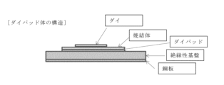
- a DBC substrate using a Cu plate having a thickness of 150 ⁇ m as a Cu die pad was used on a 0.63 mm AlN ceramic substrate having a size suitable for a prototype die size. The size of the die pad portion is 25 mm ⁇ 17 mm, and the size of the ceramic is 33 mm ⁇ 30 mm.
- a dummy chip Si substrate, 9.25 mm square, 0.2 mm thick
- a temperature measuring resistor simulating a semiconductor chip (die) and a heater resistor was used.
- a paste was applied to the entire surface on the joining side of the die pad so as to have a thickness of 200 ⁇ m, and the die was allowed to stand thereon and sintered.
- a die bonding body in which the die and the die pad were bonded was obtained.
- a paste sintered body having a thickness of 120 ⁇ m was present between the die and the die pad, and the die and the die pad were bonded.
- the die of the die bonding body and the inner lead of the lead frame were connected by wire bonding using an Au bonding wire to obtain a wire bonding body.
- the obtained wire bonded body was brought into contact with a water-cooled heat sink via grease to perform a heat radiation test.
- the heat dissipation test was performed by applying a power of 100 W to the die (dummy chip) and calculating the temperature at which the die becomes a steady state by the resistance value of the die. As a result of this heat dissipation test, it was found that the die temperature was 120 ° C. and the steady state was reached three minutes after the start of power application. Table 1 summarizes the results.
- the area where the paste was applied was the area covered by the sintered body as it was by sintering, and the area of the area did not change before and after sintering.
- Example 2 The same material as in Example 1 was prepared, and the same operation was performed except for the area of application of the paste, and the paste was applied to obtain a bonded body.
- the paste application was performed by applying the Cu paste so as to cover only 80% of the area on the Cu die pad. More specifically, the Cu paste was applied so that the center of the Cu paste overlapped with the center of the Cu die pad, and the shape of the Cu paste was the same as the shape of the Cu die pad. A power equivalent to 100 W was applied to the dummy chip, and a temperature at which the dummy chip reached a steady state was calculated from the resistance of the chip. The measurement temperature was 123 ° C.
- Example 3 The same material as in Example 1 was prepared, and the same operation was performed except for the area of application of the paste, and the paste was applied to obtain a bonded body.
- the paste application was performed by applying the Cu paste so as to cover only 60% of the area on the Cu die pad. More specifically, the Cu paste was applied so that the center of the Cu paste overlapped with the center of the Cu die pad, and the shape of the Cu paste was the same as the shape of the Cu die pad. A power equivalent to 100 W was applied to the dummy chip, and a temperature at which the dummy chip reached a steady state was calculated from the resistance of the chip. The measurement temperature was 130 ° C.
- Example 4 was performed in the same manner as in Example 1 except that the area and thickness of the paste were changed.
- Example 5 Example 5 was performed in the same manner as in Example 2 except that the thickness of the paste was changed.
- Example 1 The same material as in Example 1 was prepared, and the same operation was performed except for the area of application of the paste, and the paste was applied to obtain a bonded body. Regarding the area of the paste application, the paste application was performed by applying the Cu paste on the Cu plate so as to cover only the square region covered by the die. The measurement temperature was 135 ° C.
- Example 2 The same material as in Example 1 was prepared, and the same operation was performed except for the area of application of the paste, and the paste was applied to obtain a bonded body.
- the paste application area the paste was applied by applying a Cu paste so as to cover only a 40% area on the Cu die pad. A power equivalent to 100 W was applied to the dummy chip, and a temperature at which the dummy chip reached a steady state was calculated from the resistance of the chip. The measurement temperature was 134 ° C.
- the present invention is an industrially useful invention.
Landscapes
- Die Bonding (AREA)
- Cooling Or The Like Of Semiconductors Or Solid State Devices (AREA)
- Container, Conveyance, Adherence, Positioning, Of Wafer (AREA)
Abstract
セラミックス基板上に接合されたダイパッド、及びダイパッド上に接着されたダイを含む半導体デバイスであって、ダイがダイパッド上に金属粉ペーストの焼結体によって接着されており、金属粉ペーストの焼結体は、ダイパッドの表面上に塗布された金属粉ペーストの焼結体であり、金属粉ペーストの焼結体は、ダイパッドの表面上において、ダイの載置された領域と、ダイの載置されない領域とを、被覆する焼結体であり、金属粉ペーストの焼結体の厚みが、50~200μmの範囲にある、半導体デバイスによって、放熱特性を向上させた半導体デバイスを提供する。
Description
本発明は、半導体デバイスに関する。
パワーデバイスをモジュール化する場合、パワーデバイス間を接続するための基板として、ダイパッドとなる金属配線(以降ダイパッドと表示)付絶縁基板であるDBC(Direct Bonded Copper)基板、又は、AMC(Active Metal Brazed Copper)基板が用いられる(特許文献1)。次世代パワーデバイスは、小型化され、パワー密度が上がり、使用温度範囲が従来のMax175℃からMax250℃になることが予想されている。パワーデバイスからの放熱は重要となる。
本発明者の知見によると、上記のような構成のセラミック基板、ダイパッドとなる金属配線、及びダイの構造体において、さらに放熱特性を向上させるためには、ダイパッドとなる金属配線に用いられる金属板(例えば銅板)の厚みを増やすという手段がある。しかし、単にダイパッドの厚みを増やした場合には、DBC基板、または、AMC基板を作製する際に熱的な特性(例えば熱膨張係数)の相違によって、セラミック基板の割れや、ダイパッドのセラミック基板からの剥離等の不備が生じやすくなることがわかった。
したがって、本開示の目的は、従来使用している程度の厚みの金属板であって、セラミック基板に接合された金属板をダイパッドとして使用しつつ、放熱特性を向上させた半導体デバイスを提供することにある。
本発明者は、これまでの鋭意研究の結果、ダイとダイパッドの接着に使用される焼結型ダイアタッチ材を、ダイに覆われる領域を超えて、意図的に広い領域に塗布し、同時にその厚みを意図的に増大させることによって、ダイからの放熱特性を向上できることを見いだして、本発明に到達した。
したがって、本発明は、次の(1)を含む。
(1)
セラミックス基板上に接合されたダイパッド、及びダイパッド上に接着されたダイを含む半導体デバイスであって、
ダイがダイパッド上に金属粉ペーストの焼結体によって接着されており、
金属粉ペーストの焼結体は、ダイパッドの表面上に塗布された金属粉ペーストの焼結体であり、
金属粉ペーストの焼結体は、ダイパッドの表面上において、ダイの載置された領域と、ダイの載置されない領域とを、被覆する焼結体であり、
金属粉ペーストの焼結体の厚みが、50~200μmの範囲にある、半導体デバイス。
(1)
セラミックス基板上に接合されたダイパッド、及びダイパッド上に接着されたダイを含む半導体デバイスであって、
ダイがダイパッド上に金属粉ペーストの焼結体によって接着されており、
金属粉ペーストの焼結体は、ダイパッドの表面上に塗布された金属粉ペーストの焼結体であり、
金属粉ペーストの焼結体は、ダイパッドの表面上において、ダイの載置された領域と、ダイの載置されない領域とを、被覆する焼結体であり、
金属粉ペーストの焼結体の厚みが、50~200μmの範囲にある、半導体デバイス。
本発明によれば、従来使用している程度の厚みの銅板をダイパッドとして使用しつつ、半導体デバイスの放熱特性を向上させることができ、大きな構成の変更を伴わないために、生産性の点で不利となることがない。
以下に本発明を実施の態様をあげて詳細に説明する。本発明は以下にあげる具体的な実施の態様に限定されるものではない。
[半導体デバイスの製造]
本発明による半導体デバイスは、DBC(Direct Bonding Copper)基板、または、AMC(Active Metal Copper)基板(以下絶縁性基板とする)のダイパッドに金属粉ペーストを塗布し、その上にダイを載置した後に焼結する工程を含む製造方法であって、金属粉ペーストをダイパッドの表面上において、ダイの載置される領域とダイの載置されない領域とに塗布されたものとする方法によって、製造することができる。
[半導体デバイスの製造]
本発明による半導体デバイスは、DBC(Direct Bonding Copper)基板、または、AMC(Active Metal Copper)基板(以下絶縁性基板とする)のダイパッドに金属粉ペーストを塗布し、その上にダイを載置した後に焼結する工程を含む製造方法であって、金属粉ペーストをダイパッドの表面上において、ダイの載置される領域とダイの載置されない領域とに塗布されたものとする方法によって、製造することができる。
このようにして得られた半導体デバイスは、ダイとダイパッドが金属粉ペーストの焼結体によって接着されたダイボンディング体を有する半導体デバイスであって、金属粉ペーストの焼結体はダイパッドの表面上に塗布された金属粉ペーストの焼結体であり、金属粉ペーストの焼結体はダイパッドの表面上において、ダイの載置された領域とダイの載置されない領域とを被覆する焼結体となっている。
[ダイ]
ダイ(半導体チップ)は、ダイパッドへ接着されて固定される。さらに固定されたダイ(半導体チップ)の各電極とインナーリードとをボンディングワイヤ等で接続し、シリコーンゲルやモールド樹脂によって包埋して、半導体デバイスとする。ダイとしては、公知の材質を用いて製造されたダイ(半導体チップ)を使用することができ、材質として、例えば、Si(シリコン)、SiC(シリコンカーバイド)、GaN(ガリウムナイトライド)、Ga2O3(ガリウムオキサイド)を使用することができる。
ダイ(半導体チップ)は、ダイパッドへ接着されて固定される。さらに固定されたダイ(半導体チップ)の各電極とインナーリードとをボンディングワイヤ等で接続し、シリコーンゲルやモールド樹脂によって包埋して、半導体デバイスとする。ダイとしては、公知の材質を用いて製造されたダイ(半導体チップ)を使用することができ、材質として、例えば、Si(シリコン)、SiC(シリコンカーバイド)、GaN(ガリウムナイトライド)、Ga2O3(ガリウムオキサイド)を使用することができる。
[ダイパッド]
ダイパッドの材質は、例えば、Cu(銅)、Al(アルミニウム)、CuW(銅タングステン)、CuMo(銅モリブデン)を使用することができる。
ダイパッドの材質は、例えば、Cu(銅)、Al(アルミニウム)、CuW(銅タングステン)、CuMo(銅モリブデン)を使用することができる。
[ダイボンディング体]
ダイとダイパッドは接着されてダイボンディング体を形成する。このダイボンディング体のダイ部分とリードフレームとが電気的に接続され、モールド樹脂やシリコーンゲルによって包埋されて、耐熱性(放熱性)に優れた半導体デバイスとなる。このダイボンディング体は、ダイパッドの表面上において、ダイの載置された領域とダイの載置されない領域とを被覆する焼結体を備えており、熱伝導性に優れた特性を実現できるものであり、本発明はダイボンディング体及びその製造方法にもある。
ダイとダイパッドは接着されてダイボンディング体を形成する。このダイボンディング体のダイ部分とリードフレームとが電気的に接続され、モールド樹脂やシリコーンゲルによって包埋されて、耐熱性(放熱性)に優れた半導体デバイスとなる。このダイボンディング体は、ダイパッドの表面上において、ダイの載置された領域とダイの載置されない領域とを被覆する焼結体を備えており、熱伝導性に優れた特性を実現できるものであり、本発明はダイボンディング体及びその製造方法にもある。
[ダイとダイパッドの接着]
ダイとダイパッドは、ダイパッドの表面上に塗布された金属粉ペースト上にダイを載置した後に焼結することによって接着される。この接着部分は、金属粉ペーストの焼結体となっており、この焼結体の形成によって、接着が行われる。この接着は、ダイパッドの表面上において、ダイの載置された領域とダイの載置されない領域とを被覆する焼結体を備えるように行われて、熱伝導性に優れた特性を実現できるものである。
ダイとダイパッドは、ダイパッドの表面上に塗布された金属粉ペースト上にダイを載置した後に焼結することによって接着される。この接着部分は、金属粉ペーストの焼結体となっており、この焼結体の形成によって、接着が行われる。この接着は、ダイパッドの表面上において、ダイの載置された領域とダイの載置されない領域とを被覆する焼結体を備えるように行われて、熱伝導性に優れた特性を実現できるものである。
[金属粉ペースト]
金属粉ペーストとしては、半導体デバイスの特性を毀損しない程度の低温で焼結可能であるものであれば、特に制約はなく、公知の金属粉ペーストを使用することができる。例えば、金属粉、溶媒、バインダー樹脂、および所望により添加剤を含む、金属粉ペーストを使用することができる。好適な実施の態様において、溶媒、バインダー樹脂、添加剤は、焼結によって除去可能な化合物が使用される。好適な実施の態様において、金属粉としては、例えば平均粒径が10nm~500nmの範囲のサイズ、ナノサイズ、サブミクロンサイズ、これらのサイズの粉と扁平な金属粉を組み合わせの金属粉を使用することができる。金属粉の形状には、特に制約はなく、例えば、球状、回転楕円体状、あるいはこれらが扁平となった形状の金属粉を使用することができ、これらの形状の金属粉が混合された金属粉であってもよい。金属粉の金属としては、例えばAg、Cu、Ag-Cuの合金から選択された金属を使用することができる。あるいは金属粉を、Agで被覆されたCu粉の形態とすることができる。好適な実施の態様において、金属粉としてCu粉を使用することができる。溶媒としては、ペースト作製に公知の溶媒を使用することができ、このような溶媒として例えばα-テルピネオール、ブチルカルビトールをあげることができる。バインダー樹脂としては、ペースト作製に公知のバインダー樹脂を使用することができ、焼結温度で分解するものであればよく、例えばセルロース系、アクリル系、エポキシ系、フェノール系等のバインダー樹脂を挙げることができる。さらに、このようなバインダー樹脂として例えばポリビニールプチラール樹脂、エチルセルロースをあげることができる。
金属粉ペーストとしては、半導体デバイスの特性を毀損しない程度の低温で焼結可能であるものであれば、特に制約はなく、公知の金属粉ペーストを使用することができる。例えば、金属粉、溶媒、バインダー樹脂、および所望により添加剤を含む、金属粉ペーストを使用することができる。好適な実施の態様において、溶媒、バインダー樹脂、添加剤は、焼結によって除去可能な化合物が使用される。好適な実施の態様において、金属粉としては、例えば平均粒径が10nm~500nmの範囲のサイズ、ナノサイズ、サブミクロンサイズ、これらのサイズの粉と扁平な金属粉を組み合わせの金属粉を使用することができる。金属粉の形状には、特に制約はなく、例えば、球状、回転楕円体状、あるいはこれらが扁平となった形状の金属粉を使用することができ、これらの形状の金属粉が混合された金属粉であってもよい。金属粉の金属としては、例えばAg、Cu、Ag-Cuの合金から選択された金属を使用することができる。あるいは金属粉を、Agで被覆されたCu粉の形態とすることができる。好適な実施の態様において、金属粉としてCu粉を使用することができる。溶媒としては、ペースト作製に公知の溶媒を使用することができ、このような溶媒として例えばα-テルピネオール、ブチルカルビトールをあげることができる。バインダー樹脂としては、ペースト作製に公知のバインダー樹脂を使用することができ、焼結温度で分解するものであればよく、例えばセルロース系、アクリル系、エポキシ系、フェノール系等のバインダー樹脂を挙げることができる。さらに、このようなバインダー樹脂として例えばポリビニールプチラール樹脂、エチルセルロースをあげることができる。
[焼結]
金属粉ペーストの焼結は、例えば200~400℃、好ましくは200~300℃の範囲の温度によって、例えば、表面酸化物が不安定であるAg等の金属においては、大気雰囲気下で、表面酸化物が安定であるCu等の金属においては不活性ガス雰囲気下又は還元ガス雰囲気下、好ましくは還元ガス雰囲気下で、行うことができる。
金属粉ペーストの焼結は、例えば200~400℃、好ましくは200~300℃の範囲の温度によって、例えば、表面酸化物が不安定であるAg等の金属においては、大気雰囲気下で、表面酸化物が安定であるCu等の金属においては不活性ガス雰囲気下又は還元ガス雰囲気下、好ましくは還元ガス雰囲気下で、行うことができる。
[被覆領域比率]
ダイの載置に先立って、ダイパッドの表面上に金属粉ペーストを塗布する。塗布された金属粉ペーストは焼結によって焼結体となるので、ダイパッドの表面上の金属粉ペーストが塗布された領域は、焼結によって、金属粉ペーストの焼結体によって被覆された領域となる。本発明において、金属粉ペーストの焼結体によって被覆された領域は、ダイパッドの表面上において、ダイの載置された領域と、ダイの載置されない領域とを含む。
ダイの載置に先立って、ダイパッドの表面上に金属粉ペーストを塗布する。塗布された金属粉ペーストは焼結によって焼結体となるので、ダイパッドの表面上の金属粉ペーストが塗布された領域は、焼結によって、金属粉ペーストの焼結体によって被覆された領域となる。本発明において、金属粉ペーストの焼結体によって被覆された領域は、ダイパッドの表面上において、ダイの載置された領域と、ダイの載置されない領域とを含む。
ダイパッドの表面上の金属粉ペーストの焼結体の被覆する領域において、ダイの載置された領域の面積と、ダイの載置されない領域の面積との比率は、例えば1.05以上、1.1以上、1.2以上、1.3以上、1.4以上、1.5以上、1.8以上、1.9以上、2.0以上とすることができ、例えば1.05~10.0の範囲、1.5~10.0の範囲、2.0~10.0の範囲とすることができる。
ダイパッドの接合される側の片面の表面の面積から載置されるダイの面積を引いた面積に対する、ダイパッドの表面上の金属粉ペーストの焼結体の被覆する領域の面積から載置されるダイの面積を引いた面積の比率は、すなわち、 次の式:
[ダイパッドの表面の面積 - 載置されるダイの面積]/[ダイパッドの表面上の金属粉ペーストの焼結体の被覆領域の面積 - 載置されるダイの面積]
で表される比率は、例えば1.1以上、1.2以上、1.3以上とすることができ、例えば1.1~4.0の範囲、1.5~4.0の範囲、1.0~3.0の範囲とすることができる。
[ダイパッドの表面の面積 - 載置されるダイの面積]/[ダイパッドの表面上の金属粉ペーストの焼結体の被覆領域の面積 - 載置されるダイの面積]
で表される比率は、例えば1.1以上、1.2以上、1.3以上とすることができ、例えば1.1~4.0の範囲、1.5~4.0の範囲、1.0~3.0の範囲とすることができる。
好適な実施の態様において、金属粉ペーストの焼結体において、ダイの載置された領域の面積に対する、ダイパッドの表面上において金属粉ペーストの焼結体の被覆する面積の比(「ダイパッドの表面上において金属粉ペーストの焼結体の被覆する面積」/「ダイの載置された領域の面積」)の値を、例えば2.50以上とすることができ、好ましくは2.50~5.00の範囲とすることができる。
好適な実施の態様において、金属粉ペーストの焼結体において、焼結体が形成された側のダイパッドの表面の面積に対する、ダイパッドの表面上において金属粉ペーストの焼結体の被覆する面積の比(「ダイパッドの表面上において金属粉ペーストの焼結体の被覆する面積」/「ダイパッドの面積」)の値を、例えば0.40~1.00の範囲とすることができる。
このように、金属粉ペーストの焼結体によって被覆された領域を、ダイパッドの表面上において、ダイの載置されない領域にも設けることによって、動作時にダイから発熱を、効率的に取り去ることが可能であると本発明者は考えている。
[空隙率]
好適な実施の態様において、焼結体は、網目構造を呈するものとなっている。本発明において網目構造とは、金属粉が焼結した構造体が、焼結した金属粉の間に隙間のないち密な構造になることなく、溶融した金属粉が連結した構造となって、焼結した金属粉の間に空間部を有した構造をいう。この網目構造には、例えば0.1μm~数μm程度の多数の空隙が含まれており、この程度が空隙率として表現される。本発明において空隙率とは、焼結体を、ダイパッドに垂直な平面で切断した断面に対してSEM観察することによって、空隙と認められる黒色領域の面積と焼結された材料が充填されている灰色領域の面積の総和に占める、空隙と認められる黒色領域の面積の割合を表現した値である。好適な実施の態様において、空隙率は、例えば0.15~0.5の範囲、好ましくは0.2~0.4の範囲、さらに好ましくは0.25~0.35の範囲とすることができる。このような空隙率とした場合には、ダイパッド部分の厚みが焼結体により厚くなったことに伴う応力の緩和に役立つと本発明者は考えている。
好適な実施の態様において、焼結体は、網目構造を呈するものとなっている。本発明において網目構造とは、金属粉が焼結した構造体が、焼結した金属粉の間に隙間のないち密な構造になることなく、溶融した金属粉が連結した構造となって、焼結した金属粉の間に空間部を有した構造をいう。この網目構造には、例えば0.1μm~数μm程度の多数の空隙が含まれており、この程度が空隙率として表現される。本発明において空隙率とは、焼結体を、ダイパッドに垂直な平面で切断した断面に対してSEM観察することによって、空隙と認められる黒色領域の面積と焼結された材料が充填されている灰色領域の面積の総和に占める、空隙と認められる黒色領域の面積の割合を表現した値である。好適な実施の態様において、空隙率は、例えば0.15~0.5の範囲、好ましくは0.2~0.4の範囲、さらに好ましくは0.25~0.35の範囲とすることができる。このような空隙率とした場合には、ダイパッド部分の厚みが焼結体により厚くなったことに伴う応力の緩和に役立つと本発明者は考えている。
[焼結体の厚み]
好適な実施の態様において、金属粉ペーストの焼結体は、例えば50~200μmの範囲、好ましくは60~180μmの範囲の厚みとすることができる。金属粉ペーストの塗布の厚みは、焼結体がこのような範囲の厚みとなることを目安として、適宜設定することができる。本願発明に係る金属粉ペーストの焼結体の厚みの範囲は、従来、ダイとダイパッドとの接合に必要と考えられていた厚みの範囲よりも、大きな値となっている。これによって、ダイからの放熱特性を向上できたものと本発明者は考えている。また、上述のように、好適な実施の態様において、本願発明では、金属粉ペーストの焼結体によって被覆された領域を、ダイパッドの表面上において、ダイの載置されない領域にも設けることとしており、このような一見すると、接合に寄与しないと予想される範囲にまで焼結体の形成の領域を広げて、同時に、一見すると放熱に不利に思われるほどに接合体の厚みを厚くすることで、これらの予想に反して、本願発明のダイパッド接合体は、ダイからの放熱特性が向上されたものとなっている。
好適な実施の態様において、金属粉ペーストの焼結体は、例えば50~200μmの範囲、好ましくは60~180μmの範囲の厚みとすることができる。金属粉ペーストの塗布の厚みは、焼結体がこのような範囲の厚みとなることを目安として、適宜設定することができる。本願発明に係る金属粉ペーストの焼結体の厚みの範囲は、従来、ダイとダイパッドとの接合に必要と考えられていた厚みの範囲よりも、大きな値となっている。これによって、ダイからの放熱特性を向上できたものと本発明者は考えている。また、上述のように、好適な実施の態様において、本願発明では、金属粉ペーストの焼結体によって被覆された領域を、ダイパッドの表面上において、ダイの載置されない領域にも設けることとしており、このような一見すると、接合に寄与しないと予想される範囲にまで焼結体の形成の領域を広げて、同時に、一見すると放熱に不利に思われるほどに接合体の厚みを厚くすることで、これらの予想に反して、本願発明のダイパッド接合体は、ダイからの放熱特性が向上されたものとなっている。
[好適な実施の態様]
好適な実施の態様において、本発明は、次の(1)以下にもある。
(1)
セラミックス基板上に接合されたダイパッド、及びダイパッド上に接着されたダイを含む半導体デバイスであって、
ダイがダイパッド上に金属粉ペーストの焼結体によって接着されており、
金属粉ペーストの焼結体は、ダイパッドの表面上に塗布された金属粉ペーストの焼結体であり、
金属粉ペーストの焼結体は、ダイパッドの表面上において、ダイの載置された領域と、ダイの載置されない領域とを、被覆する焼結体であり、
金属粉ペーストの焼結体の厚みが、50~200μmの範囲にある、半導体デバイス。
(2)
金属粉ペーストが、銅粉ペーストである、(1)に記載の半導体デバイス。
(3)
金属粉ペーストの焼結体において、ダイの載置された領域の面積に対する、ダイパッドの表面上において金属粉ペーストの焼結体の被覆する面積の比(「ダイパッドの表面上において金属粉ペーストの焼結体の被覆する面積」/「ダイの載置された領域の面積」)の値が、2.50以上である、(1)~(2)のいずれかに記載の半導体デバイス。
(4)
「ダイパッドの表面上において金属粉ペーストの焼結体の被覆する面積」/「ダイの載置された領域の面積」の値が、2.50~5.00の範囲にある、(1)~(3)のいずれかに記載の半導体デバイス。
(5)
金属粉ペーストの焼結体において、焼結体が形成された側のダイパッドの表面の面積に対する、ダイパッドの表面上において金属粉ペーストの焼結体の被覆する面積の比(「ダイパッドの表面上において金属粉ペーストの焼結体の被覆する面積」/「ダイパッドの面積」)の値が、0.40~1.00の範囲にある、(1)~(2)のいずれかに記載の半導体デバイス。
好適な実施の態様において、本発明は、次の(1)以下にもある。
(1)
セラミックス基板上に接合されたダイパッド、及びダイパッド上に接着されたダイを含む半導体デバイスであって、
ダイがダイパッド上に金属粉ペーストの焼結体によって接着されており、
金属粉ペーストの焼結体は、ダイパッドの表面上に塗布された金属粉ペーストの焼結体であり、
金属粉ペーストの焼結体は、ダイパッドの表面上において、ダイの載置された領域と、ダイの載置されない領域とを、被覆する焼結体であり、
金属粉ペーストの焼結体の厚みが、50~200μmの範囲にある、半導体デバイス。
(2)
金属粉ペーストが、銅粉ペーストである、(1)に記載の半導体デバイス。
(3)
金属粉ペーストの焼結体において、ダイの載置された領域の面積に対する、ダイパッドの表面上において金属粉ペーストの焼結体の被覆する面積の比(「ダイパッドの表面上において金属粉ペーストの焼結体の被覆する面積」/「ダイの載置された領域の面積」)の値が、2.50以上である、(1)~(2)のいずれかに記載の半導体デバイス。
(4)
「ダイパッドの表面上において金属粉ペーストの焼結体の被覆する面積」/「ダイの載置された領域の面積」の値が、2.50~5.00の範囲にある、(1)~(3)のいずれかに記載の半導体デバイス。
(5)
金属粉ペーストの焼結体において、焼結体が形成された側のダイパッドの表面の面積に対する、ダイパッドの表面上において金属粉ペーストの焼結体の被覆する面積の比(「ダイパッドの表面上において金属粉ペーストの焼結体の被覆する面積」/「ダイパッドの面積」)の値が、0.40~1.00の範囲にある、(1)~(2)のいずれかに記載の半導体デバイス。
以下に実施例をあげて、本発明をさらに詳細に説明する。本発明は、以下の実施例に限定されるものではない。
[実施例1]
Cuペーストとして、サブミクロンCu粉(JX金属製)を、アクリル樹脂を含むターピネオール中に、Cu粉の割合がペースト全体に対して85wt%となるように分散させて、Cuペーストを調整した。
絶縁性基板として試作のダイサイズに適合したサイズの0.63mmのAlNセラミック基板にCuダイパッドとして150μm厚のCuプレートを使用したDBC基板を用いた。ダイパッド部のサイズは25mmx17mmであり、セラミックの大きさは33mmx30mmである。
チップ温度を測定するため、半導体チップ(ダイ)を模した温度測定用抵抗体とヒーター用抵抗体がついたダミーチップ(Si基板、9.25mm角、厚さ0.2mm)を用いた。
Cuペーストとして、サブミクロンCu粉(JX金属製)を、アクリル樹脂を含むターピネオール中に、Cu粉の割合がペースト全体に対して85wt%となるように分散させて、Cuペーストを調整した。
絶縁性基板として試作のダイサイズに適合したサイズの0.63mmのAlNセラミック基板にCuダイパッドとして150μm厚のCuプレートを使用したDBC基板を用いた。ダイパッド部のサイズは25mmx17mmであり、セラミックの大きさは33mmx30mmである。
チップ温度を測定するため、半導体チップ(ダイ)を模した温度測定用抵抗体とヒーター用抵抗体がついたダミーチップ(Si基板、9.25mm角、厚さ0.2mm)を用いた。
ダイとダイパッドを接合するために、ダイパッドの接合する側の面の全面に、ペーストを厚さ200μmとなるように塗布して、この上にダイを静置し、焼結した。
このようにして、ダイとダイパッドが接合されたダイボンディング体を得た。
得られたダイボンディング体は、ダイとダイパッドの間にペーストの焼結体が、厚さ120μmで存在して、ダイとダイパッドとを接合していた。
ダイボンディング体のダイと、リードフレームのインナーリードとを、Auボンディングワイヤを用いたワイヤボンディングによって結線して、ワイヤボンディング体を得た。
このようにして、ダイとダイパッドが接合されたダイボンディング体を得た。
得られたダイボンディング体は、ダイとダイパッドの間にペーストの焼結体が、厚さ120μmで存在して、ダイとダイパッドとを接合していた。
ダイボンディング体のダイと、リードフレームのインナーリードとを、Auボンディングワイヤを用いたワイヤボンディングによって結線して、ワイヤボンディング体を得た。
得られたワイヤボンディング体を、グリースを介して水冷ヒートシンクに接触させて、放熱性試験を行った。
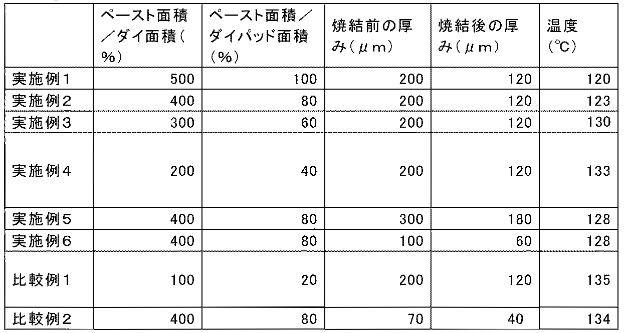
放熱性試験は、ダイ(ダミーチップ)へ100Wの電力を印加して、定常状態となる温度をダイの抵抗値によって算出することによって、行った。この放熱性試験の結果、電力印加開始から3分後に、ダイ温度が120℃で定常状態となることがわかった。
この結果をまとめて表1に示す。なお、ペーストの塗布された領域は焼結によってそのまま焼結体の被覆する領域となっており、焼結の前後で領域の面積に変化はなかった。
放熱性試験は、ダイ(ダミーチップ)へ100Wの電力を印加して、定常状態となる温度をダイの抵抗値によって算出することによって、行った。この放熱性試験の結果、電力印加開始から3分後に、ダイ温度が120℃で定常状態となることがわかった。
この結果をまとめて表1に示す。なお、ペーストの塗布された領域は焼結によってそのまま焼結体の被覆する領域となっており、焼結の前後で領域の面積に変化はなかった。
(実施例2)
実施例1と同じ材料を用意して、ペーストの塗布の面積以外については同様の操作を行って、ペーストを塗布し、ボンディング体を得た。
上記ペーストの塗布の面積に関して、ペーストの塗布は、Cuダイパッド上において、80%の領域だけを覆うように、Cuペーストを塗布して行った。より具体的には、Cuペーストの中心とCuダイパッドの中心とが重なるように、かつ、Cuペースト形状とCuダイパッド形状とが同じになるように、Cuペーストを塗布した。
ダミーチップには100W相当の電力を印加し、定常状態となる温度を、チップの抵抗により算出した。測定温度は、123℃であった。
実施例1と同じ材料を用意して、ペーストの塗布の面積以外については同様の操作を行って、ペーストを塗布し、ボンディング体を得た。
上記ペーストの塗布の面積に関して、ペーストの塗布は、Cuダイパッド上において、80%の領域だけを覆うように、Cuペーストを塗布して行った。より具体的には、Cuペーストの中心とCuダイパッドの中心とが重なるように、かつ、Cuペースト形状とCuダイパッド形状とが同じになるように、Cuペーストを塗布した。
ダミーチップには100W相当の電力を印加し、定常状態となる温度を、チップの抵抗により算出した。測定温度は、123℃であった。
(実施例3)
実施例1と同じ材料を用意して、ペーストの塗布の面積以外については同様の操作を行って、ペーストを塗布し、ボンディング体を得た。
上記ペーストの塗布の面積に関して、ペーストの塗布は、Cuダイパッド上において、60%の領域だけを覆うように、Cuペーストを塗布して行った。より具体的には、Cuペーストの中心とCuダイパッドの中心とが重なるように、かつ、Cuペースト形状とCuダイパッド形状とが同じになるように、Cuペーストを塗布した。
ダミーチップには100W相当の電力を印加し、定常状態となる温度を、チップの抵抗により算出した。測定温度は、130℃であった。
実施例1と同じ材料を用意して、ペーストの塗布の面積以外については同様の操作を行って、ペーストを塗布し、ボンディング体を得た。
上記ペーストの塗布の面積に関して、ペーストの塗布は、Cuダイパッド上において、60%の領域だけを覆うように、Cuペーストを塗布して行った。より具体的には、Cuペーストの中心とCuダイパッドの中心とが重なるように、かつ、Cuペースト形状とCuダイパッド形状とが同じになるように、Cuペーストを塗布した。
ダミーチップには100W相当の電力を印加し、定常状態となる温度を、チップの抵抗により算出した。測定温度は、130℃であった。
(実施例4)
ペーストの塗布について、面積及び厚みを変更したことを除いて、実施例1と同様にして、実施例4を行った。
ペーストの塗布について、面積及び厚みを変更したことを除いて、実施例1と同様にして、実施例4を行った。
(実施例5、6)
ペーストの塗布について、厚みを変更したことを除いて、実施例2と同様にして、実施例5、6を行った。
ペーストの塗布について、厚みを変更したことを除いて、実施例2と同様にして、実施例5、6を行った。
(比較例1)
実施例1と同じ材料を用意して、ペーストの塗布の面積以外については同様の操作を行って、ペーストを塗布し、ボンディング体を得た。
上記ペーストの塗布の面積に関して、ペーストの塗布は、Cuプレート上において、ダイによって覆われる四角形の領域だけを覆うように、Cuペーストを塗布して行った。測定温度は135℃であった。
実施例1と同じ材料を用意して、ペーストの塗布の面積以外については同様の操作を行って、ペーストを塗布し、ボンディング体を得た。
上記ペーストの塗布の面積に関して、ペーストの塗布は、Cuプレート上において、ダイによって覆われる四角形の領域だけを覆うように、Cuペーストを塗布して行った。測定温度は135℃であった。
(比較例2)
実施例1と同じ材料を用意して、ペーストの塗布の面積以外については同様の操作を行って、ペーストを塗布し、ボンディング体を得た。
上記ペーストの塗布の面積に関して、ペーストの塗布は、Cuダイパッド上において、40%の領域だけを覆うように、Cuペーストを塗布して行った。
ダミーチップには100W相当の電力を印加し、定常状態となる温度を、チップの抵抗により算出した。測定温度は、134℃であった。
実施例1と同じ材料を用意して、ペーストの塗布の面積以外については同様の操作を行って、ペーストを塗布し、ボンディング体を得た。
上記ペーストの塗布の面積に関して、ペーストの塗布は、Cuダイパッド上において、40%の領域だけを覆うように、Cuペーストを塗布して行った。
ダミーチップには100W相当の電力を印加し、定常状態となる温度を、チップの抵抗により算出した。測定温度は、134℃であった。
本発明によれば、放熱特性を向上させた半導体デバイスを得ることができる。本発明は産業上有用な発明である。
Claims (5)
- セラミックス基板上に接合されたダイパッド、及びダイパッド上に接着されたダイを含む半導体デバイスであって、
ダイがダイパッド上に金属粉ペーストの焼結体によって接着されており、
金属粉ペーストの焼結体は、ダイパッドの表面上に塗布された金属粉ペーストの焼結体であり、
金属粉ペーストの焼結体は、ダイパッドの表面上において、ダイの載置された領域と、ダイの載置されない領域とを、被覆する焼結体であり、
金属粉ペーストの焼結体の厚みが、50~200μmの範囲にある、半導体デバイス。 - 金属粉ペーストが、銅粉ペーストである、請求項1に記載の半導体デバイス。
- 金属粉ペーストの焼結体において、ダイの載置された領域の面積に対する、ダイパッドの表面上において金属粉ペーストの焼結体の被覆する面積の比(「ダイパッドの表面上において金属粉ペーストの焼結体の被覆する面積」/「ダイの載置された領域の面積」)の値が、2.50以上である、請求項1~2のいずれかに記載の半導体デバイス。
- 「ダイパッドの表面上において金属粉ペーストの焼結体の被覆する面積」/「ダイの載置された領域の面積」の値が、2.50~5.00の範囲にある、請求項1~3のいずれかに記載の半導体デバイス。
- 金属粉ペーストの焼結体において、焼結体が形成された側のダイパッドの表面の面積に対する、ダイパッドの表面上において金属粉ペーストの焼結体の被覆する面積の比(「ダイパッドの表面上において金属粉ペーストの焼結体の被覆する面積」/「ダイパッドの面積」)の値が、0.40~1.00の範囲にある、請求項1~2のいずれかに記載の半導体デバイス。
Applications Claiming Priority (2)
| Application Number | Priority Date | Filing Date | Title |
|---|---|---|---|
| JP2018140554A JP6712620B2 (ja) | 2018-07-26 | 2018-07-26 | 半導体デバイス |
| JP2018-140554 | 2018-07-26 |
Publications (1)
| Publication Number | Publication Date |
|---|---|
| WO2020021853A1 true WO2020021853A1 (ja) | 2020-01-30 |
Family
ID=69181565
Family Applications (1)
| Application Number | Title | Priority Date | Filing Date |
|---|---|---|---|
| PCT/JP2019/021617 Ceased WO2020021853A1 (ja) | 2018-07-26 | 2019-05-30 | 半導体デバイス |
Country Status (3)
| Country | Link |
|---|---|
| JP (1) | JP6712620B2 (ja) |
| TW (1) | TWI703110B (ja) |
| WO (1) | WO2020021853A1 (ja) |
Citations (5)
| Publication number | Priority date | Publication date | Assignee | Title |
|---|---|---|---|---|
| JP2004039988A (ja) * | 2002-07-05 | 2004-02-05 | Shinko Electric Ind Co Ltd | 素子搭載用回路基板及び電子装置 |
| JP2007201346A (ja) * | 2006-01-30 | 2007-08-09 | Mitsuboshi Belting Ltd | セラミックス回路基板及びその製造方法 |
| JP2011249257A (ja) * | 2010-05-31 | 2011-12-08 | Hitachi Ltd | 焼結銀ペースト材料及び半導体チップ接合方法 |
| JP2014022579A (ja) * | 2012-07-19 | 2014-02-03 | Rohm Co Ltd | パワーモジュール半導体装置 |
| JP2016031999A (ja) * | 2014-07-28 | 2016-03-07 | 株式会社ノリタケカンパニーリミテド | 放熱性基板 |
Family Cites Families (3)
| Publication number | Priority date | Publication date | Assignee | Title |
|---|---|---|---|---|
| JP2002033411A (ja) * | 2000-07-13 | 2002-01-31 | Nec Corp | ヒートスプレッダ付き半導体装置及びその製造方法 |
| JP6819597B2 (ja) * | 2015-09-07 | 2021-01-27 | 昭和電工マテリアルズ株式会社 | 接合体及び半導体装置 |
| AU2017317329B2 (en) * | 2016-08-22 | 2019-05-02 | Senju Metal Industry Co., Ltd. | Metallic sintered bonding body and die bonding method |
-
2018
- 2018-07-26 JP JP2018140554A patent/JP6712620B2/ja active Active
-
2019
- 2019-05-30 WO PCT/JP2019/021617 patent/WO2020021853A1/ja not_active Ceased
- 2019-06-20 TW TW108121450A patent/TWI703110B/zh active
Patent Citations (5)
| Publication number | Priority date | Publication date | Assignee | Title |
|---|---|---|---|---|
| JP2004039988A (ja) * | 2002-07-05 | 2004-02-05 | Shinko Electric Ind Co Ltd | 素子搭載用回路基板及び電子装置 |
| JP2007201346A (ja) * | 2006-01-30 | 2007-08-09 | Mitsuboshi Belting Ltd | セラミックス回路基板及びその製造方法 |
| JP2011249257A (ja) * | 2010-05-31 | 2011-12-08 | Hitachi Ltd | 焼結銀ペースト材料及び半導体チップ接合方法 |
| JP2014022579A (ja) * | 2012-07-19 | 2014-02-03 | Rohm Co Ltd | パワーモジュール半導体装置 |
| JP2016031999A (ja) * | 2014-07-28 | 2016-03-07 | 株式会社ノリタケカンパニーリミテド | 放熱性基板 |
Also Published As
| Publication number | Publication date |
|---|---|
| JP6712620B2 (ja) | 2020-06-24 |
| TW202010726A (zh) | 2020-03-16 |
| JP2020017671A (ja) | 2020-01-30 |
| TWI703110B (zh) | 2020-09-01 |
Similar Documents
| Publication | Publication Date | Title |
|---|---|---|
| JP5664625B2 (ja) | 半導体装置、セラミックス回路基板及び半導体装置の製造方法 | |
| JP6319643B2 (ja) | セラミックス−銅接合体およびその製造方法 | |
| JP6146007B2 (ja) | 接合体の製造方法、パワーモジュールの製造方法、パワーモジュール用基板及びパワーモジュール | |
| EP3093882A1 (en) | Electronic circuit device | |
| US10290602B2 (en) | Semiconductor device and method of making semiconductor device | |
| JPWO2020091008A1 (ja) | 金属層付き炭素質部材、及び、熱伝導板 | |
| TWI642154B (zh) | 電源模組用基板及其製造方法、電源模組 | |
| CN106415822B (zh) | 半导体封装体及其制造方法 | |
| CN108305838B (zh) | 一种不含有机物的低温芯片贴装方法及芯片贴装结构 | |
| JP6613929B2 (ja) | Ag下地層付き金属部材、Ag下地層付き絶縁回路基板、半導体装置、ヒートシンク付き絶縁回路基板、及び、Ag下地層付き金属部材の製造方法 | |
| WO2017150096A1 (ja) | 半導体装置 | |
| JP2015216160A (ja) | 電力用半導体装置および電力用半導体装置の製造方法 | |
| JP2017065935A (ja) | セラミックス回路基板 | |
| JP6893593B2 (ja) | Niナノ粒子を用いた接合材料及び接合構造体 | |
| JP2014160707A (ja) | 接合体の製造方法、パワーモジュールの製造方法、及びパワーモジュール | |
| JP6712620B2 (ja) | 半導体デバイス | |
| JP6574234B2 (ja) | 半導体デバイス | |
| JP6983119B2 (ja) | 放熱板、半導体パッケージおよび半導体装置 | |
| JP2012064616A (ja) | 高放熱型電子部品収納用パッケージ | |
| JP2014187252A (ja) | 接合材、接合構造体およびその製造方法、並びに半導体モジュール | |
| WO2020240866A1 (ja) | 半導体デバイス | |
| JP4485893B2 (ja) | 電子部品収納用パッケージおよび電子装置 | |
| TWI701783B (zh) | 半導體裝置 | |
| JP3559457B2 (ja) | ロウ材 | |
| WO2013021983A1 (ja) | 半導体装置及びその製造方法 |
Legal Events
| Date | Code | Title | Description |
|---|---|---|---|
| 121 | Ep: the epo has been informed by wipo that ep was designated in this application |
Ref document number: 19842297 Country of ref document: EP Kind code of ref document: A1 |
|
| DPE1 | Request for preliminary examination filed after expiration of 19th month from priority date (pct application filed from 20040101) | ||
| NENP | Non-entry into the national phase |
Ref country code: DE |
|
| 122 | Ep: pct application non-entry in european phase |
Ref document number: 19842297 Country of ref document: EP Kind code of ref document: A1 |