WO2020003678A1 - 機能性膜の製造方法、乾燥装置、及び機能性膜の製造装置 - Google Patents
機能性膜の製造方法、乾燥装置、及び機能性膜の製造装置 Download PDFInfo
- Publication number
- WO2020003678A1 WO2020003678A1 PCT/JP2019/014664 JP2019014664W WO2020003678A1 WO 2020003678 A1 WO2020003678 A1 WO 2020003678A1 JP 2019014664 W JP2019014664 W JP 2019014664W WO 2020003678 A1 WO2020003678 A1 WO 2020003678A1
- Authority
- WO
- WIPO (PCT)
- Prior art keywords
- substrate
- temperature
- drying
- functional film
- roll
- Prior art date
Links
- 238000001035 drying Methods 0.000 title claims abstract description 63
- 238000004519 manufacturing process Methods 0.000 title claims abstract description 42
- 239000012528 membrane Substances 0.000 title claims abstract 7
- 239000000758 substrate Substances 0.000 claims abstract description 150
- 238000000034 method Methods 0.000 claims abstract description 88
- 238000000576 coating method Methods 0.000 claims abstract description 50
- 239000011248 coating agent Substances 0.000 claims abstract description 38
- 239000000463 material Substances 0.000 claims abstract description 38
- 230000008859 change Effects 0.000 claims abstract description 31
- 230000032258 transport Effects 0.000 claims description 74
- 230000008569 process Effects 0.000 claims description 48
- 238000007641 inkjet printing Methods 0.000 claims description 7
- 239000010408 film Substances 0.000 description 86
- 239000010410 layer Substances 0.000 description 76
- 238000012360 testing method Methods 0.000 description 28
- 238000002347 injection Methods 0.000 description 23
- 239000007924 injection Substances 0.000 description 23
- 238000010438 heat treatment Methods 0.000 description 16
- 239000002904 solvent Substances 0.000 description 14
- 238000012546 transfer Methods 0.000 description 12
- -1 polyethylene terephthalate Polymers 0.000 description 8
- 229910052751 metal Inorganic materials 0.000 description 7
- 239000002184 metal Substances 0.000 description 7
- ZWEHNKRNPOVVGH-UHFFFAOYSA-N 2-Butanone Chemical compound CCC(C)=O ZWEHNKRNPOVVGH-UHFFFAOYSA-N 0.000 description 6
- CSCPPACGZOOCGX-UHFFFAOYSA-N Acetone Chemical compound CC(C)=O CSCPPACGZOOCGX-UHFFFAOYSA-N 0.000 description 6
- YMWUJEATGCHHMB-UHFFFAOYSA-N Dichloromethane Chemical compound ClCCl YMWUJEATGCHHMB-UHFFFAOYSA-N 0.000 description 6
- XEKOWRVHYACXOJ-UHFFFAOYSA-N Ethyl acetate Chemical compound CCOC(C)=O XEKOWRVHYACXOJ-UHFFFAOYSA-N 0.000 description 6
- YXFVVABEGXRONW-UHFFFAOYSA-N Toluene Chemical compound CC1=CC=CC=C1 YXFVVABEGXRONW-UHFFFAOYSA-N 0.000 description 6
- 150000004696 coordination complex Chemical class 0.000 description 5
- 238000005520 cutting process Methods 0.000 description 5
- 230000005525 hole transport Effects 0.000 description 5
- 238000005424 photoluminescence Methods 0.000 description 5
- BASFCYQUMIYNBI-UHFFFAOYSA-N platinum Chemical compound [Pt] BASFCYQUMIYNBI-UHFFFAOYSA-N 0.000 description 5
- 239000000126 substance Substances 0.000 description 5
- HEDRZPFGACZZDS-UHFFFAOYSA-N Chloroform Chemical compound ClC(Cl)Cl HEDRZPFGACZZDS-UHFFFAOYSA-N 0.000 description 4
- WYURNTSHIVDZCO-UHFFFAOYSA-N Tetrahydrofuran Chemical compound C1CCOC1 WYURNTSHIVDZCO-UHFFFAOYSA-N 0.000 description 4
- 230000004888 barrier function Effects 0.000 description 4
- ZYGHJZDHTFUPRJ-UHFFFAOYSA-N coumarin Chemical compound C1=CC=C2OC(=O)C=CC2=C1 ZYGHJZDHTFUPRJ-UHFFFAOYSA-N 0.000 description 4
- 239000002019 doping agent Substances 0.000 description 4
- 229920005989 resin Polymers 0.000 description 4
- 239000011347 resin Substances 0.000 description 4
- 239000007787 solid Substances 0.000 description 4
- 239000010409 thin film Substances 0.000 description 4
- 238000002834 transmittance Methods 0.000 description 4
- XUIMIQQOPSSXEZ-UHFFFAOYSA-N Silicon Chemical compound [Si] XUIMIQQOPSSXEZ-UHFFFAOYSA-N 0.000 description 3
- 230000015572 biosynthetic process Effects 0.000 description 3
- 229910052697 platinum Inorganic materials 0.000 description 3
- 238000007639 printing Methods 0.000 description 3
- 229910052710 silicon Inorganic materials 0.000 description 3
- 239000010703 silicon Substances 0.000 description 3
- 238000004804 winding Methods 0.000 description 3
- 229910052725 zinc Inorganic materials 0.000 description 3
- 239000011701 zinc Substances 0.000 description 3
- SCYULBFZEHDVBN-UHFFFAOYSA-N 1,1-Dichloroethane Chemical compound CC(Cl)Cl SCYULBFZEHDVBN-UHFFFAOYSA-N 0.000 description 2
- VQGHOUODWALEFC-UHFFFAOYSA-N 2-phenylpyridine Chemical compound C1=CC=CC=C1C1=CC=CC=N1 VQGHOUODWALEFC-UHFFFAOYSA-N 0.000 description 2
- QTBSBXVTEAMEQO-UHFFFAOYSA-M Acetate Chemical compound CC([O-])=O QTBSBXVTEAMEQO-UHFFFAOYSA-M 0.000 description 2
- IJGRMHOSHXDMSA-UHFFFAOYSA-N Atomic nitrogen Chemical compound N#N IJGRMHOSHXDMSA-UHFFFAOYSA-N 0.000 description 2
- DKPFZGUDAPQIHT-UHFFFAOYSA-N Butyl acetate Natural products CCCCOC(C)=O DKPFZGUDAPQIHT-UHFFFAOYSA-N 0.000 description 2
- OKTJSMMVPCPJKN-UHFFFAOYSA-N Carbon Chemical compound [C] OKTJSMMVPCPJKN-UHFFFAOYSA-N 0.000 description 2
- VEXZGXHMUGYJMC-UHFFFAOYSA-M Chloride anion Chemical compound [Cl-] VEXZGXHMUGYJMC-UHFFFAOYSA-M 0.000 description 2
- 229910052693 Europium Inorganic materials 0.000 description 2
- CTQNGGLPUBDAKN-UHFFFAOYSA-N O-Xylene Chemical compound CC1=CC=CC=C1C CTQNGGLPUBDAKN-UHFFFAOYSA-N 0.000 description 2
- 239000004698 Polyethylene Substances 0.000 description 2
- 239000004743 Polypropylene Substances 0.000 description 2
- KAESVJOAVNADME-UHFFFAOYSA-N Pyrrole Chemical compound C=1C=CNC=1 KAESVJOAVNADME-UHFFFAOYSA-N 0.000 description 2
- NRCMAYZCPIVABH-UHFFFAOYSA-N Quinacridone Chemical compound N1C2=CC=CC=C2C(=O)C2=C1C=C1C(=O)C3=CC=CC=C3NC1=C2 NRCMAYZCPIVABH-UHFFFAOYSA-N 0.000 description 2
- SMWDFEZZVXVKRB-UHFFFAOYSA-N Quinoline Chemical compound N1=CC=CC2=CC=CC=C21 SMWDFEZZVXVKRB-UHFFFAOYSA-N 0.000 description 2
- HCHKCACWOHOZIP-UHFFFAOYSA-N Zinc Chemical compound [Zn] HCHKCACWOHOZIP-UHFFFAOYSA-N 0.000 description 2
- XLOMVQKBTHCTTD-UHFFFAOYSA-N Zinc monoxide Chemical compound [Zn]=O XLOMVQKBTHCTTD-UHFFFAOYSA-N 0.000 description 2
- 150000004945 aromatic hydrocarbons Chemical class 0.000 description 2
- QVGXLLKOCUKJST-UHFFFAOYSA-N atomic oxygen Chemical compound [O] QVGXLLKOCUKJST-UHFFFAOYSA-N 0.000 description 2
- 238000007611 bar coating method Methods 0.000 description 2
- 229910052790 beryllium Inorganic materials 0.000 description 2
- 229910052799 carbon Inorganic materials 0.000 description 2
- 150000001875 compounds Chemical class 0.000 description 2
- 239000004020 conductor Substances 0.000 description 2
- 229960000956 coumarin Drugs 0.000 description 2
- 235000001671 coumarin Nutrition 0.000 description 2
- 238000009826 distribution Methods 0.000 description 2
- 238000005485 electric heating Methods 0.000 description 2
- 239000003759 ester based solvent Substances 0.000 description 2
- 239000004210 ether based solvent Substances 0.000 description 2
- 125000001495 ethyl group Chemical group [H]C([H])([H])C([H])([H])* 0.000 description 2
- 230000001747 exhibiting effect Effects 0.000 description 2
- 238000007756 gravure coating Methods 0.000 description 2
- FUZZWVXGSFPDMH-UHFFFAOYSA-N hexanoic acid Chemical compound CCCCCC(O)=O FUZZWVXGSFPDMH-UHFFFAOYSA-N 0.000 description 2
- 238000003384 imaging method Methods 0.000 description 2
- AMGQUBHHOARCQH-UHFFFAOYSA-N indium;oxotin Chemical compound [In].[Sn]=O AMGQUBHHOARCQH-UHFFFAOYSA-N 0.000 description 2
- 229910052741 iridium Inorganic materials 0.000 description 2
- 230000001678 irradiating effect Effects 0.000 description 2
- 239000005453 ketone based solvent Substances 0.000 description 2
- 229910044991 metal oxide Inorganic materials 0.000 description 2
- 150000004706 metal oxides Chemical class 0.000 description 2
- 238000007645 offset printing Methods 0.000 description 2
- WCPAKWJPBJAGKN-UHFFFAOYSA-N oxadiazole Chemical compound C1=CON=N1 WCPAKWJPBJAGKN-UHFFFAOYSA-N 0.000 description 2
- 229910052760 oxygen Inorganic materials 0.000 description 2
- 239000001301 oxygen Substances 0.000 description 2
- 125000002080 perylenyl group Chemical group C1(=CC=C2C=CC=C3C4=CC=CC5=CC=CC(C1=C23)=C45)* 0.000 description 2
- CSHWQDPOILHKBI-UHFFFAOYSA-N peryrene Natural products C1=CC(C2=CC=CC=3C2=C2C=CC=3)=C3C2=CC=CC3=C1 CSHWQDPOILHKBI-UHFFFAOYSA-N 0.000 description 2
- 229920000573 polyethylene Polymers 0.000 description 2
- 229920000139 polyethylene terephthalate Polymers 0.000 description 2
- 239000005020 polyethylene terephthalate Substances 0.000 description 2
- 229920001155 polypropylene Polymers 0.000 description 2
- 229920000123 polythiophene Polymers 0.000 description 2
- 150000004032 porphyrins Chemical class 0.000 description 2
- 238000012545 processing Methods 0.000 description 2
- 238000005096 rolling process Methods 0.000 description 2
- 238000007650 screen-printing Methods 0.000 description 2
- 238000007789 sealing Methods 0.000 description 2
- 238000005507 spraying Methods 0.000 description 2
- YLQBMQCUIZJEEH-UHFFFAOYSA-N tetrahydrofuran Natural products C=1C=COC=1 YLQBMQCUIZJEEH-UHFFFAOYSA-N 0.000 description 2
- XOLBLPGZBRYERU-UHFFFAOYSA-N tin dioxide Chemical compound O=[Sn]=O XOLBLPGZBRYERU-UHFFFAOYSA-N 0.000 description 2
- 229910001887 tin oxide Inorganic materials 0.000 description 2
- 238000011144 upstream manufacturing Methods 0.000 description 2
- 239000008096 xylene Substances 0.000 description 2
- YVTHLONGBIQYBO-UHFFFAOYSA-N zinc indium(3+) oxygen(2-) Chemical compound [O--].[Zn++].[In+3] YVTHLONGBIQYBO-UHFFFAOYSA-N 0.000 description 2
- NGQSLSMAEVWNPU-YTEMWHBBSA-N 1,2-bis[(e)-2-phenylethenyl]benzene Chemical compound C=1C=CC=CC=1/C=C/C1=CC=CC=C1\C=C\C1=CC=CC=C1 NGQSLSMAEVWNPU-YTEMWHBBSA-N 0.000 description 1
- SHXCHSNZIGEBFL-UHFFFAOYSA-N 1,3-benzothiazole;zinc Chemical compound [Zn].C1=CC=C2SC=NC2=C1 SHXCHSNZIGEBFL-UHFFFAOYSA-N 0.000 description 1
- KLCLIOISYBHYDZ-UHFFFAOYSA-N 1,4,4-triphenylbuta-1,3-dienylbenzene Chemical compound C=1C=CC=CC=1C(C=1C=CC=CC=1)=CC=C(C=1C=CC=CC=1)C1=CC=CC=C1 KLCLIOISYBHYDZ-UHFFFAOYSA-N 0.000 description 1
- UIWLITBBFICQKW-UHFFFAOYSA-N 1h-benzo[h]quinolin-2-one Chemical compound C1=CC=C2C3=NC(O)=CC=C3C=CC2=C1 UIWLITBBFICQKW-UHFFFAOYSA-N 0.000 description 1
- DWYHDSLIWMUSOO-UHFFFAOYSA-N 2-phenyl-1h-benzimidazole Chemical compound C1=CC=CC=C1C1=NC2=CC=CC=C2N1 DWYHDSLIWMUSOO-UHFFFAOYSA-N 0.000 description 1
- AJWRRBADQOOFSF-UHFFFAOYSA-N C1=CC=C2OC([Zn])=NC2=C1 Chemical compound C1=CC=C2OC([Zn])=NC2=C1 AJWRRBADQOOFSF-UHFFFAOYSA-N 0.000 description 1
- UXYHZIYEDDINQH-UHFFFAOYSA-N C1=CNC2=C3C=NN=C3C=CC2=C1 Chemical compound C1=CNC2=C3C=NN=C3C=CC2=C1 UXYHZIYEDDINQH-UHFFFAOYSA-N 0.000 description 1
- RYGMFSIKBFXOCR-UHFFFAOYSA-N Copper Chemical compound [Cu] RYGMFSIKBFXOCR-UHFFFAOYSA-N 0.000 description 1
- 229910052692 Dysprosium Inorganic materials 0.000 description 1
- 229920012266 Poly(ether sulfone) PES Polymers 0.000 description 1
- 229920000265 Polyparaphenylene Polymers 0.000 description 1
- 239000004372 Polyvinyl alcohol Substances 0.000 description 1
- 229910052581 Si3N4 Inorganic materials 0.000 description 1
- VYPSYNLAJGMNEJ-UHFFFAOYSA-N Silicium dioxide Chemical compound O=[Si]=O VYPSYNLAJGMNEJ-UHFFFAOYSA-N 0.000 description 1
- BQCADISMDOOEFD-UHFFFAOYSA-N Silver Chemical compound [Ag] BQCADISMDOOEFD-UHFFFAOYSA-N 0.000 description 1
- 229910052771 Terbium Inorganic materials 0.000 description 1
- XBDYBAVJXHJMNQ-UHFFFAOYSA-N Tetrahydroanthracene Natural products C1=CC=C2C=C(CCCC3)C3=CC2=C1 XBDYBAVJXHJMNQ-UHFFFAOYSA-N 0.000 description 1
- DGEZNRSVGBDHLK-UHFFFAOYSA-N [1,10]phenanthroline Chemical compound C1=CN=C2C3=NC=CC=C3C=CC2=C1 DGEZNRSVGBDHLK-UHFFFAOYSA-N 0.000 description 1
- 239000011354 acetal resin Substances 0.000 description 1
- 229910052783 alkali metal Inorganic materials 0.000 description 1
- 150000001340 alkali metals Chemical class 0.000 description 1
- 229910052784 alkaline earth metal Inorganic materials 0.000 description 1
- 150000001342 alkaline earth metals Chemical class 0.000 description 1
- HSFWRNGVRCDJHI-UHFFFAOYSA-N alpha-acetylene Natural products C#C HSFWRNGVRCDJHI-UHFFFAOYSA-N 0.000 description 1
- 229910052782 aluminium Inorganic materials 0.000 description 1
- ATBAMAFKBVZNFJ-UHFFFAOYSA-N beryllium atom Chemical compound [Be] ATBAMAFKBVZNFJ-UHFFFAOYSA-N 0.000 description 1
- 238000009835 boiling Methods 0.000 description 1
- 238000005266 casting Methods 0.000 description 1
- 239000000919 ceramic Substances 0.000 description 1
- 239000008199 coating composition Substances 0.000 description 1
- 239000011365 complex material Substances 0.000 description 1
- 239000012809 cooling fluid Substances 0.000 description 1
- 229910052802 copper Inorganic materials 0.000 description 1
- 239000010949 copper Substances 0.000 description 1
- 125000004122 cyclic group Chemical group 0.000 description 1
- CUIWZLHUNCCYBL-UHFFFAOYSA-N decacyclene Chemical compound C12=C([C]34)C=CC=C4C=CC=C3C2=C2C(=C34)C=C[CH]C4=CC=CC3=C2C2=C1C1=CC=CC3=CC=CC2=C31 CUIWZLHUNCCYBL-UHFFFAOYSA-N 0.000 description 1
- 238000003618 dip coating Methods 0.000 description 1
- OGPBJKLSAFTDLK-UHFFFAOYSA-N europium atom Chemical compound [Eu] OGPBJKLSAFTDLK-UHFFFAOYSA-N 0.000 description 1
- 230000005281 excited state Effects 0.000 description 1
- JVZRCNQLWOELDU-UHFFFAOYSA-N gamma-Phenylpyridine Natural products C1=CC=CC=C1C1=CC=NC=C1 JVZRCNQLWOELDU-UHFFFAOYSA-N 0.000 description 1
- 230000009477 glass transition Effects 0.000 description 1
- PCHJSUWPFVWCPO-UHFFFAOYSA-N gold Chemical compound [Au] PCHJSUWPFVWCPO-UHFFFAOYSA-N 0.000 description 1
- 229910052737 gold Inorganic materials 0.000 description 1
- 239000010931 gold Substances 0.000 description 1
- 238000007602 hot air drying Methods 0.000 description 1
- 238000005286 illumination Methods 0.000 description 1
- 229910003437 indium oxide Inorganic materials 0.000 description 1
- PJXISJQVUVHSOJ-UHFFFAOYSA-N indium(iii) oxide Chemical compound [O-2].[O-2].[O-2].[In+3].[In+3] PJXISJQVUVHSOJ-UHFFFAOYSA-N 0.000 description 1
- 238000007733 ion plating Methods 0.000 description 1
- GKOZUEZYRPOHIO-UHFFFAOYSA-N iridium atom Chemical compound [Ir] GKOZUEZYRPOHIO-UHFFFAOYSA-N 0.000 description 1
- 239000002346 layers by function Substances 0.000 description 1
- 239000003446 ligand Substances 0.000 description 1
- 238000005259 measurement Methods 0.000 description 1
- 229910052976 metal sulfide Inorganic materials 0.000 description 1
- 150000002739 metals Chemical class 0.000 description 1
- 229910052757 nitrogen Inorganic materials 0.000 description 1
- 239000011368 organic material Substances 0.000 description 1
- 150000004866 oxadiazoles Chemical class 0.000 description 1
- DGBWPZSGHAXYGK-UHFFFAOYSA-N perinone Chemical compound C12=NC3=CC=CC=C3N2C(=O)C2=CC=C3C4=C2C1=CC=C4C(=O)N1C2=CC=CC=C2N=C13 DGBWPZSGHAXYGK-UHFFFAOYSA-N 0.000 description 1
- 230000000737 periodic effect Effects 0.000 description 1
- FIZIRKROSLGMPL-UHFFFAOYSA-N phenoxazin-1-one Chemical compound C1=CC=C2N=C3C(=O)C=CC=C3OC2=C1 FIZIRKROSLGMPL-UHFFFAOYSA-N 0.000 description 1
- UOMHBFAJZRZNQD-UHFFFAOYSA-N phenoxazone Natural products C1=CC=C2OC3=CC(=O)C=CC3=NC2=C1 UOMHBFAJZRZNQD-UHFFFAOYSA-N 0.000 description 1
- 229920006255 plastic film Polymers 0.000 description 1
- 239000002985 plastic film Substances 0.000 description 1
- 238000007747 plating Methods 0.000 description 1
- 229920003227 poly(N-vinyl carbazole) Polymers 0.000 description 1
- 229920001200 poly(ethylene-vinyl acetate) Polymers 0.000 description 1
- 229920000548 poly(silane) polymer Polymers 0.000 description 1
- 229920001197 polyacetylene Polymers 0.000 description 1
- 229920006350 polyacrylonitrile resin Polymers 0.000 description 1
- 229920000767 polyaniline Polymers 0.000 description 1
- 229920005668 polycarbonate resin Polymers 0.000 description 1
- 239000004431 polycarbonate resin Substances 0.000 description 1
- 229920001225 polyester resin Polymers 0.000 description 1
- 239000004645 polyester resin Substances 0.000 description 1
- 239000011112 polyethylene naphthalate Substances 0.000 description 1
- 229920002098 polyfluorene Polymers 0.000 description 1
- 229920001721 polyimide Polymers 0.000 description 1
- 239000009719 polyimide resin Substances 0.000 description 1
- 229920000642 polymer Polymers 0.000 description 1
- 229920006254 polymer film Polymers 0.000 description 1
- 239000002861 polymer material Substances 0.000 description 1
- 230000000379 polymerizing effect Effects 0.000 description 1
- 229920000098 polyolefin Polymers 0.000 description 1
- 229920005672 polyolefin resin Polymers 0.000 description 1
- 229920006324 polyoxymethylene Polymers 0.000 description 1
- 229920005990 polystyrene resin Polymers 0.000 description 1
- 229920002451 polyvinyl alcohol Polymers 0.000 description 1
- JEXVQSWXXUJEMA-UHFFFAOYSA-N pyrazol-3-one Chemical compound O=C1C=CN=N1 JEXVQSWXXUJEMA-UHFFFAOYSA-N 0.000 description 1
- 150000003219 pyrazolines Chemical class 0.000 description 1
- 229910052761 rare earth metal Inorganic materials 0.000 description 1
- 150000002910 rare earth metals Chemical class 0.000 description 1
- 238000000611 regression analysis Methods 0.000 description 1
- YYMBJDOZVAITBP-UHFFFAOYSA-N rubrene Chemical compound C1=CC=CC=C1C(C1=C(C=2C=CC=CC=2)C2=CC=CC=C2C(C=2C=CC=CC=2)=C11)=C(C=CC=C2)C2=C1C1=CC=CC=C1 YYMBJDOZVAITBP-UHFFFAOYSA-N 0.000 description 1
- HQVNEWCFYHHQES-UHFFFAOYSA-N silicon nitride Chemical compound N12[Si]34N5[Si]62N3[Si]51N64 HQVNEWCFYHHQES-UHFFFAOYSA-N 0.000 description 1
- 229910052814 silicon oxide Inorganic materials 0.000 description 1
- 229910052709 silver Inorganic materials 0.000 description 1
- 239000004332 silver Substances 0.000 description 1
- 239000000243 solution Substances 0.000 description 1
- 238000004528 spin coating Methods 0.000 description 1
- 238000004544 sputter deposition Methods 0.000 description 1
- 125000005504 styryl group Chemical group 0.000 description 1
- IFLREYGFSNHWGE-UHFFFAOYSA-N tetracene Chemical compound C1=CC=CC2=CC3=CC4=CC=CC=C4C=C3C=C21 IFLREYGFSNHWGE-UHFFFAOYSA-N 0.000 description 1
- VLLMWSRANPNYQX-UHFFFAOYSA-N thiadiazole Chemical compound C1=CSN=N1.C1=CSN=N1 VLLMWSRANPNYQX-UHFFFAOYSA-N 0.000 description 1
- 229910052723 transition metal Inorganic materials 0.000 description 1
- 150000003624 transition metals Chemical class 0.000 description 1
- 239000012780 transparent material Substances 0.000 description 1
- ODHXBMXNKOYIBV-UHFFFAOYSA-N triphenylamine Chemical compound C1=CC=CC=C1N(C=1C=CC=CC=1)C1=CC=CC=C1 ODHXBMXNKOYIBV-UHFFFAOYSA-N 0.000 description 1
- 238000001771 vacuum deposition Methods 0.000 description 1
- 239000002023 wood Substances 0.000 description 1
- 239000011787 zinc oxide Substances 0.000 description 1
Images


Classifications
-
- B—PERFORMING OPERATIONS; TRANSPORTING
- B05—SPRAYING OR ATOMISING IN GENERAL; APPLYING FLUENT MATERIALS TO SURFACES, IN GENERAL
- B05D—PROCESSES FOR APPLYING FLUENT MATERIALS TO SURFACES, IN GENERAL
- B05D3/00—Pretreatment of surfaces to which liquids or other fluent materials are to be applied; After-treatment of applied coatings, e.g. intermediate treating of an applied coating preparatory to subsequent applications of liquids or other fluent materials
- B05D3/02—Pretreatment of surfaces to which liquids or other fluent materials are to be applied; After-treatment of applied coatings, e.g. intermediate treating of an applied coating preparatory to subsequent applications of liquids or other fluent materials by baking
-
- F—MECHANICAL ENGINEERING; LIGHTING; HEATING; WEAPONS; BLASTING
- F26—DRYING
- F26B—DRYING SOLID MATERIALS OR OBJECTS BY REMOVING LIQUID THEREFROM
- F26B13/00—Machines and apparatus for drying fabrics, fibres, yarns, or other materials in long lengths, with progressive movement
- F26B13/10—Arrangements for feeding, heating or supporting materials; Controlling movement, tension or position of materials
- F26B13/101—Supporting materials without tension, e.g. on or between foraminous belts
- F26B13/103—Supporting materials without tension, e.g. on or between foraminous belts with mechanical supporting means, e.g. belts, rollers, and fluid impingement arrangement having a displacing effect on the materials
-
- B—PERFORMING OPERATIONS; TRANSPORTING
- B41—PRINTING; LINING MACHINES; TYPEWRITERS; STAMPS
- B41F—PRINTING MACHINES OR PRESSES
- B41F23/00—Devices for treating the surfaces of sheets, webs, or other articles in connection with printing
- B41F23/04—Devices for treating the surfaces of sheets, webs, or other articles in connection with printing by heat drying, by cooling, by applying powders
-
- B—PERFORMING OPERATIONS; TRANSPORTING
- B41—PRINTING; LINING MACHINES; TYPEWRITERS; STAMPS
- B41M—PRINTING, DUPLICATING, MARKING, OR COPYING PROCESSES; COLOUR PRINTING
- B41M7/00—After-treatment of prints, e.g. heating, irradiating, setting of the ink, protection of the printed stock
-
- F—MECHANICAL ENGINEERING; LIGHTING; HEATING; WEAPONS; BLASTING
- F26—DRYING
- F26B—DRYING SOLID MATERIALS OR OBJECTS BY REMOVING LIQUID THEREFROM
- F26B13/00—Machines and apparatus for drying fabrics, fibres, yarns, or other materials in long lengths, with progressive movement
- F26B13/10—Arrangements for feeding, heating or supporting materials; Controlling movement, tension or position of materials
-
- F—MECHANICAL ENGINEERING; LIGHTING; HEATING; WEAPONS; BLASTING
- F26—DRYING
- F26B—DRYING SOLID MATERIALS OR OBJECTS BY REMOVING LIQUID THEREFROM
- F26B23/00—Heating arrangements
- F26B23/04—Heating arrangements using electric heating
-
- F—MECHANICAL ENGINEERING; LIGHTING; HEATING; WEAPONS; BLASTING
- F26—DRYING
- F26B—DRYING SOLID MATERIALS OR OBJECTS BY REMOVING LIQUID THEREFROM
- F26B3/00—Drying solid materials or objects by processes involving the application of heat
- F26B3/28—Drying solid materials or objects by processes involving the application of heat by radiation, e.g. from the sun
- F26B3/30—Drying solid materials or objects by processes involving the application of heat by radiation, e.g. from the sun from infrared-emitting elements
-
- H—ELECTRICITY
- H05—ELECTRIC TECHNIQUES NOT OTHERWISE PROVIDED FOR
- H05B—ELECTRIC HEATING; ELECTRIC LIGHT SOURCES NOT OTHERWISE PROVIDED FOR; CIRCUIT ARRANGEMENTS FOR ELECTRIC LIGHT SOURCES, IN GENERAL
- H05B33/00—Electroluminescent light sources
- H05B33/10—Apparatus or processes specially adapted to the manufacture of electroluminescent light sources
-
- H—ELECTRICITY
- H10—SEMICONDUCTOR DEVICES; ELECTRIC SOLID-STATE DEVICES NOT OTHERWISE PROVIDED FOR
- H10K—ORGANIC ELECTRIC SOLID-STATE DEVICES
- H10K50/00—Organic light-emitting devices
- H10K50/10—OLEDs or polymer light-emitting diodes [PLED]
- H10K50/11—OLEDs or polymer light-emitting diodes [PLED] characterised by the electroluminescent [EL] layers
-
- H—ELECTRICITY
- H10—SEMICONDUCTOR DEVICES; ELECTRIC SOLID-STATE DEVICES NOT OTHERWISE PROVIDED FOR
- H10K—ORGANIC ELECTRIC SOLID-STATE DEVICES
- H10K71/00—Manufacture or treatment specially adapted for the organic devices covered by this subclass
- H10K71/10—Deposition of organic active material
- H10K71/12—Deposition of organic active material using liquid deposition, e.g. spin coating
- H10K71/13—Deposition of organic active material using liquid deposition, e.g. spin coating using printing techniques, e.g. ink-jet printing or screen printing
- H10K71/135—Deposition of organic active material using liquid deposition, e.g. spin coating using printing techniques, e.g. ink-jet printing or screen printing using ink-jet printing
-
- H—ELECTRICITY
- H10—SEMICONDUCTOR DEVICES; ELECTRIC SOLID-STATE DEVICES NOT OTHERWISE PROVIDED FOR
- H10K—ORGANIC ELECTRIC SOLID-STATE DEVICES
- H10K71/00—Manufacture or treatment specially adapted for the organic devices covered by this subclass
- H10K71/40—Thermal treatment, e.g. annealing in the presence of a solvent vapour
-
- B—PERFORMING OPERATIONS; TRANSPORTING
- B05—SPRAYING OR ATOMISING IN GENERAL; APPLYING FLUENT MATERIALS TO SURFACES, IN GENERAL
- B05C—APPARATUS FOR APPLYING FLUENT MATERIALS TO SURFACES, IN GENERAL
- B05C9/00—Apparatus or plant for applying liquid or other fluent material to surfaces by means not covered by any preceding group, or in which the means of applying the liquid or other fluent material is not important
- B05C9/08—Apparatus or plant for applying liquid or other fluent material to surfaces by means not covered by any preceding group, or in which the means of applying the liquid or other fluent material is not important for applying liquid or other fluent material and performing an auxiliary operation
- B05C9/14—Apparatus or plant for applying liquid or other fluent material to surfaces by means not covered by any preceding group, or in which the means of applying the liquid or other fluent material is not important for applying liquid or other fluent material and performing an auxiliary operation the auxiliary operation involving heating or cooling
-
- H—ELECTRICITY
- H10—SEMICONDUCTOR DEVICES; ELECTRIC SOLID-STATE DEVICES NOT OTHERWISE PROVIDED FOR
- H10K—ORGANIC ELECTRIC SOLID-STATE DEVICES
- H10K2102/00—Constructional details relating to the organic devices covered by this subclass
- H10K2102/301—Details of OLEDs
- H10K2102/361—Temperature
Definitions
- the present invention relates to a method for producing a functional film, a drying apparatus, and an apparatus for producing a functional film.
- the organic EL element has a functional film on the surface of the substrate.
- a film such as a functional film is formed by applying an ink containing a film material on a substrate, and then performing a drying process in a drying furnace.
- Patent Document 1 Japanese Patent Application Laid-Open No. 2002-340479 (Patent Document 1) describes that the wind speed of hot air sent into a drying furnace is controlled to prevent wind ripples on the surface quality of the film.
- the object of the present invention is to provide a method for producing a functional film, a drying device, and a device for producing a functional film, which can suppress the occurrence of streak-like unevenness on the surface of the functional film.
- the present invention provides the following [1] to [16].
- [1] A manufacturing method for manufacturing a functional film provided on an upper surface of a long substrate, On the upper surface of the substrate, an application step of applying an ink containing the material of the functional film to form a coating film, A drying step of drying the coating film while transporting the substrate, The drying step includes a first step of transporting the substrate for a first distance, during which the temperature of the substrate is increased from a first temperature to a second temperature.
- the first distance is d 1 (m)
- the first temperature is T 1 (° C.)
- the second temperature is T 2 (° C.)
- the maximum value of the instantaneous temperature change rate of the substrate is 5 ° C./sec or less.
- the drying step further includes, after the first step, a second step of transporting the substrate for a second distance and maintaining the temperature of the substrate during the second distance in a range near the second temperature.
- a drying device for drying a coating film formed on an upper surface of a long substrate A first process unit that conveys the substrate for a first distance, during which the temperature of the substrate is raised from a first temperature to a second temperature;
- the first distance is d 1 (m)
- the first temperature is T 1 (° C.)
- the second temperature is T 2 (° C.)
- the maximum value of the instantaneous temperature change rate of the substrate is 5 ° C./sec or less.
- the apparatus further includes a second process unit that conveys the substrate for a second distance and maintains the temperature of the substrate during the second process in a range near the second temperature.
- a manufacturing apparatus for manufacturing a functional film on an upper surface of a long substrate A manufacturing apparatus comprising the drying apparatus according to any one of [9] to [14].
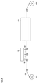
- FIG. 1 is a sectional view schematically showing a drying apparatus according to an embodiment of the present invention.
- FIG. 2A is a cross-sectional view schematically illustrating an example of a surface stepped roll.
- FIG. 2B is a cross-sectional view schematically illustrating an example of a surface stepped roll.
- FIG. 3 is a sectional view schematically showing the configuration of the organic EL device according to the first embodiment.
- FIG. 4 is a cross-sectional view schematically showing a light emitting layer forming step in the first embodiment.
- FIG. 5A is a graph in which the temperature in the first step of Test Example 1 is plotted.
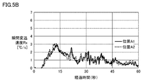
- FIG. 5B is a graph in which the instantaneous temperature change rate in the first step of Test Example 1 is plotted.
- FIG. 5A is a graph in which the temperature in the first step of Test Example 1 is plotted.
- FIG. 5B is a graph in which the instantaneous temperature change rate in the first step of Test Example 1 is plotted
- FIG. 6A is a graph in which the temperature in the first step of Test Example 2 is plotted.
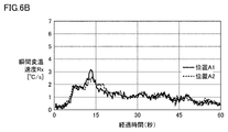
- FIG. 6B is a graph in which the instantaneous temperature change rate in the first step of Test Example 2 is plotted.
- FIG. 7A is a graph in which the temperature in the first step of Test Example 3 is plotted.
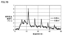
- FIG. 7B is a graph in which the instantaneous temperature change rate in the first step of Test Example 3 is plotted.
- FIG. 8A is a photoluminescence photograph of the functional film of Test Example 1.
- FIG. 8B is a photoluminescence photograph of the functional film of Test Example 3.
- the present invention is a manufacturing method for manufacturing a functional film provided on an upper surface of a long substrate, and a coating step of applying an ink containing a material for the functional film on the upper surface of the substrate to form a coating film. And a drying step of drying the coating film while transporting the substrate.
- the coating film before being subjected to the ink and the drying step contains a material for the functional film and a solvent for dispersing or dissolving the material.
- the drying step includes a first step.
- the drying step preferably includes a second step after the first step.
- the first step is a temperature raising step in which the substrate is transported for a first distance and the temperature of the substrate is raised from the first temperature to the second temperature during that time.
- the first distance is d 1 (m)
- the first temperature is T 1 (° C.)
- the second temperature is T 2 (° C.): (T 2 ⁇ T 1 ) / d 1 ⁇ 10 (1a) Satisfy the relationship.
- the second step is a constant temperature step in which the substrate is transported for a second distance and the temperature of the substrate during that time is kept in a range near the second temperature.
- the range around the second temperature is preferably T 2 ⁇ 5 ° C., and more preferably T 2 ⁇ 2 ° C.
- the first temperature T 1 and the second temperature T 2 is the value measured in the following manner.
- Arbitrary positions for measuring Tx are two different positions whose positions in the width direction are the same distance from the end (hereinafter, also referred to as “position A1” and “position A2”), and Tx measured at the two positions.
- the first temperature T 1 of the nearly matches the temperature at the start of the first step
- the second temperature T 2 is substantially equal to the temperature of the end of the first step.
- the target attainment temperature is preferably determined according to the boiling point of the solvent contained in the coating film.
- the method of measuring the temperature at the position A1 and the position A2 of the substrate is not particularly limited as long as it is a thermometer capable of measuring at intervals of 0.1 seconds, and may be a contact type or a non-contact type. Good.
- a thermometer for example, a resistance temperature detector, a thermocouple, or the like that can be attached to the position A1 and the position A2 of the substrate can be given.
- First distance d 1 is the conveying speed, on the basis of the temperature-responsive of the substrate is preferably determined as appropriate so second temperature T 2 and the target attainable temperature substantially coincide.
- the second distance d 2 is the conveying speed, the thickness of the coating film, based on the solvent content and the like of the coating film, the removal of the solvent having a target is properly determined so as to achieve the preferred.
- the transport speed of the substrate in the first step and the second step is, for example, 0.5 to 5 m / min, and preferably 1 to 3 m / min.
- First distance d 1 is the distance in the range of, for example, 1m or 5m or less.
- the second distance d 2 is the distance in the range of, for example, 2m or less than 10m.
- the maximum value of the instantaneous temperature change rate is 5 ° C./sec or less.
- the instantaneous temperature change rate is calculated every 0.1 second from the start point to the end point of the first step.
- the instantaneous temperature change rate at x seconds (0.6 seconds, 0.7 seconds, 0.8 seconds,...) After the start point (0 seconds) is R x (° C./second) from the start point.
- the instantaneous temperature change rate R x is 10 points of x-0.5 seconds to x + 0.4 seconds every 0.1 seconds.
- the maximum value of the instantaneous temperature change rate Rx at the position A1 and the position A2 is 5 ° C./sec or less, streak-like unevenness generated in the functional film can be suppressed.
- the maximum value of the instantaneous temperature change rate Rx is preferably 4 ° C./second or less, from the viewpoint of further suppressing streak-like unevenness.
- the present inventors have a case where a large temperature change occurs instantaneously in a temperature raising step such as the first step, and thereby, streak-like unevenness in a direction perpendicular to the transport direction is easily generated in the functional film. With the knowledge obtained, the present invention has been achieved. Further, in the aspect in which the substrate is transported by the transport roll, at the moment when the substrate is brought into contact with the transport roll, or before and after the contact, the knowledge that a large temperature change is likely to occur momentarily is obtained. It has been found that a large temperature change is likely to occur instantaneously at the moment of contact with the transport roll or before or after the contact with the transport roll, and a specific embodiment for carrying out the present invention has been achieved.
- FIG. 1 is a cross-sectional view schematically showing a drying device for performing a drying step.
- the drying device 100 includes a first process unit 10 and a second process unit 20.
- the substrate 1 is transported so as to sequentially pass through the first process unit 10 and the second process unit 20.
- the first process is performed in the first process unit 10, and the second process is performed in the second process unit 20.
- the substrate 1 and the first distance d 1 conveyed by sequentially contacting the carrier rolls 11a ⁇ 11f six on the lower surface of the substrate 1. During that time, the substrate 1 is heated by the heating unit 12 to increase the temperature of the substrate 1 from the first temperature to the second temperature.
- the substrate 1 and the second distance d 2 conveyed was sequentially contact transport rolls 21a ⁇ 21f of the lower surface to the six substrate 1. Meanwhile, the substrate 1 is heated by the heating unit 22 to maintain the temperature of the substrate 1 in a range near the second temperature.
- the number of transport rolls in the first process unit 10 and the second process unit 20 is not limited to six each, and if it is two or more, it can be appropriately designed according to the transport distance.
- the number of transport rolls in the first process section 10 and the second process section 20 is, for example, three to ten.
- Each transport roll has a columnar shape, and is not limited as long as the transport roll is configured to be able to transport the substrate 1 by rotating while bringing the substrate 1 into contact with the surface.
- the central portion of the transport roll may be a hollow hollow roll or a solid hollow roll.
- the surface of the transport roll may be a smooth roll having a smooth surface and contacting the entire lower surface of the substrate 1 or a stepped roll having a step and contacting a part of the lower surface of the substrate 1.
- the material of the transport roll is not particularly limited, and examples of the surface material include resin, ceramic, metal, and wood.
- the diameter of the transport roll is not particularly limited, and is, for example, 30 mm to 100 mm.
- the transport rolls 11a to 11f in the first process unit 10 and the transport rolls 21a to 21f in the second process unit 20 do not need to be all the same, and can be appropriately selected individually.
- the heating unit 12 in the first process unit 10 heats the atmosphere in the first process unit 10 by a heat source such as an electric heating plate to heat the substrate 1 even if the substrate 1 is heated by irradiating energy rays and radiating heat. Heating may be used. Examples of the energy ray include infrared rays, far infrared rays, and microwaves.
- the heating unit 12 is preferably configured to heat the substrate 1 by infrared irradiation, since the heating unit 12 can efficiently heat the substrate 1.
- the first process unit 10 preferably has a predetermined temperature distribution that monotonically increases from the first temperature T1 to the second temperature T2 over the first distance.
- a plurality of infrared irradiation devices can be provided, and the output of each infrared irradiation device can be gradually increased along the transport direction.
- the arrangement position of the heating unit 12 in the first process unit 10 is not limited, and may be arranged above the substrate 1 to be conveyed, may be arranged below the substrate 1, or may be arranged on both sides. It may be.
- the heating unit 22 in the second process unit 20 may be a heat source such as an electric heating plate even if the substrate 1 is heated by irradiating energy rays and radiating heat. In this case, the substrate 1 may be heated by heating the atmosphere in the second process section 20.
- the arrangement position of the heating unit 22 in the second process unit 20 is not limited, and may be arranged above the substrate 1 to be conveyed, may be arranged below the substrate 1, or may be arranged on both sides. It may be.
- methods for adjusting the maximum value of the instantaneous temperature change rate to 5 ° C./sec or less include a method of adjusting the transport roll, a method of adjusting the surface temperature of the temperature control roll, and the like.
- a method of adjusting the transport roll at least one of the transport rolls may be a transport roll having a low heat transfer amount to the substrate 1 (hereinafter, also referred to as a “low heat transfer transport roll”).
- the low heat transfer roll include a roll with a stepped surface having a reduced contact area with the lower surface of the substrate 1 and a hollow roll having a small heat capacity.
- the low heat transfer carrier roll preferably has an average heat capacity per width of 110 J / K or less, more preferably 80 J / K or less.
- the average heat capacity per width of the transport roll differs depending on the material of the transport roll, whether the transport roll is solid or hollow, the diameter of the transport roll, and the like.
- a hollow roll, a roll with a surface step, or the like a transport roll having an average heat capacity in the width direction of 110 J / K or less can be formed.
- all the transport rolls may be low-heat-transfer transport rolls, or only transport rolls arranged in an area where the instantaneous temperature change rate is likely to be high. It may be a low heat transfer roll.
- the transport rolls since the variable rate of temperature tends to increase the moment when the temperature of the substrate 1 is in contact with the conveyor roll in the state than the second temperature T 2 is a temperature close to the first temperature T 1, the It is preferable that the transport rolls (the transport rolls 11a, 11b, and 11c in FIG. 1) that are arranged on the upstream side of the first process unit 10 by dividing the first distance d1 into two are low heat transfer transport rolls.
- the instantaneous temperature change rate is calculated in advance, and the transfer rolls disposed around the position where the instantaneous temperature change rate exceeds 5 ° C./sec are determined.
- the adjustment may be performed by replacing the roll with a low heat transfer roll.
- FIGS. 2A and 2B are cross-sectional views schematically showing an example of a roll with a surface step.
- the surface stepped rolls 30a and 30b have a concave portion 31 and a convex portion 32 on the surface. In the concave portion 31, the lower surface of the substrate 1 does not come into contact with the roll, and the amount of heat transfer to the substrate 1 is reduced. It is configured to be smaller.
- the surface stepped roll 30 a has a convex portion 32 at an end, and a concave portion 31 at a central region sandwiched between the convex portions 32.
- the surface stepped roll 30b has a convex portion 32 at an end, and concave portions 31 and convex portions 32 are alternately formed in a central region sandwiched between the convex portions 32.
- the lower surface of the region where the coating film is provided on the substrate 1 faces the concave portion of the surface stepped roll. This is because, by reducing the amount of heat transfer particularly in the region of the substrate 1 where the coating film is provided, it is possible to more effectively suppress the occurrence of streak-like unevenness occurring in the coating film.
- the lower surface By making the lower surface of 50% or more, preferably 80% or more, and more preferably 100% of the region where the coating film is provided face the concave portion of the surface step roll, the surface step is formed. The use of the roll can greatly contribute to suppressing the occurrence of streak-like unevenness generated in the coating film.
- At least one of the transport rolls has a surface temperature of at least one.
- An adjustable transport roll (hereinafter, also referred to as a “temperature control roll”) may be used.
- the method of adjusting the surface temperature of the temperature control roll is not limited, and examples thereof include a method of passing a cooling fluid inside. It is preferable to adjust the surface temperature of the temperature control roll so that the temperature difference from the temperature of the substrate at that position is equal to or less than a predetermined value.
- the predetermined value or less is preferably 15 ° C. or less, more preferably 10 ° C.
- a determination unit for determining a temperature difference between the surface temperature of the temperature control roll and the temperature of the substrate is provided, and the surface temperature of the temperature control roll can be adjusted according to the determination result of the determination unit.
- the transport rolls since the variable rate of temperature tends to increase the moment when the temperature of the substrate 1 is in contact with the conveyor roll in the state in than the second temperature T 2 temperatures close to the first temperature T 1, the It is preferable that the transport rolls (the transport rolls 11a, 11b, and 11c in FIG. 1) that are arranged on the upstream side of the first process unit 10 at the first distance d1 divided into two are temperature control rolls.
- the instantaneous temperature change rate is calculated in advance, and the transfer rolls disposed around the position where the instantaneous temperature change rate exceeds 5 ° C./sec are determined. Adjustment may be performed by replacing the temperature control roll.
- ink is applied to the upper surface of the long substrate to form a coating film.
- the application step may be a step performed while transporting the substrate, or may be a step performed without transporting the substrate. From the viewpoint that the above-described drying step can be performed continuously after the application step. Preferably, the process is performed while the substrate is being transported.
- Examples of ink application methods include spin coating, casting, microgravure coating, gravure coating, bar coating, roll coating, wire bar coating, dip coating, spray coating, screen printing,
- a coating method such as a flexographic printing method, an offset printing method, an ink jet printing method, a capillary coating method, a nozzle coating method, or the like can be used, and from the viewpoint of obtaining a flat coating film, ink jet printing which is an ejection type coating method.
- the method is preferably used.
- the type of ink used in the application step is not particularly limited. However, as the concentration of the ink is lower and the viscosity of the ink is lower, streak-like unevenness tends to occur on the surface of the functional film. According to the present invention, even when a low-concentration ink, a low-viscosity ink, or the like is used, generation of streak-like unevenness on the surface of the functional film can be suppressed.
- ink is applied to an arbitrary region on the upper surface of the substrate according to the use of the functional film.
- the coating composition is not applied to at least one end in the width direction of the long substrate.
- One embodiment of the apparatus for producing a functional film according to the present invention includes the above-described drying apparatus. According to this embodiment, it is possible to manufacture a functional film in which the occurrence of streak-like unevenness that occurs in a direction orthogonal to the transport direction in the drying device is suppressed.
- This embodiment is a method for manufacturing an organic EL device having a functional film.
- FIG. 3 is a sectional view schematically showing the configuration of the organic EL device according to the present embodiment.
- the organic EL element 80 manufactured by the method for manufacturing an organic EL element according to the present embodiment is, for example, an organic EL lighting panel used for illumination.
- the organic EL element 80 includes a substrate 82, an anode (first electrode) 84, a light emitting layer (functional layer for organic EL) 86, and a cathode (second electrode) 88.
- the organic EL element 80 can take a form in which light is emitted from the anode 84 side or a form in which light is emitted from the cathode 88 side.
- a mode in which light is emitted from the anode 84 side will be described unless otherwise specified.
- the substrate 82 has a property of transmitting visible light (light having a wavelength of 400 nm to 800 nm).
- the substrate 82 may be a film-like substrate.
- the thickness of the substrate 82 is, for example, not less than 30 ⁇ m and not more than 700 ⁇ m.
- the substrate 82 has flexibility, and an example of the substrate 82 is a plastic film or a polymer film.
- the material of the substrate 82 include polyether sulfone (PES); polyester resins such as polyethylene terephthalate (PET) and polyethylene naphthalate (PEN); polyolefin resins such as polyethylene (PE), polypropylene (PP) and cyclic polyolefin; Resins; polycarbonate resins; polystyrene resins; polyvinyl alcohol resins; saponified ethylene-vinyl acetate copolymers; polyacrylonitrile resins; acetal resins; polyimide resins;
- a drive circuit for example, a circuit including a thin film transistor for driving the organic EL element 80 may be formed on the substrate 82.
- Such a drive circuit is usually made of a transparent material.
- a barrier film may be formed on the upper surface 82a of the substrate 82.
- the barrier film may be, for example, a film made of silicon, oxygen, and carbon, or a film made of silicon, oxygen, carbon, and nitrogen.
- examples of the material of the barrier film include silicon oxide, silicon nitride, silicon oxynitride, and the like.
- An example of the thickness of the barrier film is 100 nm or more and 10 ⁇ m or less.
- the anode 84 is provided on the upper surface 82 a of the substrate 82.
- an electrode exhibiting light transmittance is used.
- a thin film of a metal oxide, a metal sulfide, a metal or the like having a high electric conductivity can be used, and a thin film having a high light transmittance is preferably used.
- the anode 84 may have a network structure made of a conductor (for example, a metal).
- the thickness of the anode 84 can be determined in consideration of light transmittance, electric conductivity, and the like.
- the thickness of the anode 84 is usually 10 nm to 10 ⁇ m, preferably 20 nm to 1 ⁇ m, and more preferably 50 nm to 500 nm.
- the substrate 82 provided with the anode 84 may be referred to as a substrate 60 with electrodes.
- the light emitting layer 86 is a functional film provided on the anode 84 and having a function of emitting light of a predetermined wavelength.
- the optimum value of the thickness of the light emitting layer 86 differs depending on the material used, and is appropriately set so that the driving voltage and the light emission efficiency have appropriate values.
- the thickness of the light emitting layer 86 is, for example, 1 nm to 1 ⁇ m, preferably 2 nm to 500 nm, and more preferably 10 nm to 200 nm.
- the cathode 88 is provided on the light emitting layer 86.
- the thickness of the cathode 88 has an optimum value that differs depending on the material used, and is set in consideration of electrical conductivity, durability, and the like.
- the thickness of the cathode 88 is usually 10 nm to 10 ⁇ m, preferably 20 nm to 1 ⁇ m, and more preferably 50 nm to 500 nm.
- another functional film may be provided between the anode 84 and the light emitting layer 86 and between the light emitting layer 86 and the cathode 88.
- Examples of the layer configuration of the organic EL element 80 including various functional films are shown below.
- anode / emission layer / cathode b) anode / hole injection layer / emission layer / cathode c) anode / hole injection layer / emission layer / electron injection layer / cathode d) anode / hole injection layer / emission layer / Electron transport layer / electron injection layer / cathode e) anode / hole injection layer / hole transport layer / emission layer / cathode f) anode / hole injection layer / hole transport layer / emission layer / electron injection layer / cathode g H) anode / light-emitting layer / electron-injection layer / electron injection h) anode / light-emitting layer / electron-injection layer / cathode i) anode / light-emitting layer / electron-transport layer / electron injection Layer / Cathode
- the symbol “/” means that the layers on both sides of the symbol “/” are
- the hole injection layer is a functional film having a function of improving the efficiency of hole injection from the anode 84 to the light emitting layer 86.
- the hole transport layer is a functional film having a function of improving the efficiency of hole injection from the hole transport layer closer to the anode 84 to the anode 84, the hole injection layer, or the light emitting layer 86.
- the electron transport layer is a functional film having a function of improving the efficiency of electron injection from the cathode 88, the electron injection layer, or the electron transport layer closer to the cathode 88.
- the electron injection layer is a functional film having a function of improving the efficiency of electron injection from the cathode 88 to the light emitting layer 86.
- the electron injection layer may be part of the cathode.
- each functional film for the organic EL has an optimum value that differs depending on the material used, and is appropriately set so that the driving voltage and the luminous efficiency have appropriate values.
- the organic EL element 80 may include a sealing portion for sealing at least the functional film on the substrate 60 with electrodes.
- a long substrate and a long substrate with an electrode refer to a substrate and a substrate with an electrode whose length in the transport direction (X-axis direction) described later is longer than the length in the width direction (Y-axis direction). Point.
- the long electrode-equipped substrate 60 can be manufactured by forming the anode 84 in each of a plurality of element formation regions set on the upper surface 82a of the flexible long substrate 82.
- the material of the anode 84 examples include indium oxide, zinc oxide, tin oxide, indium tin oxide (Indium Tin Oxide: abbreviated ITO), indium zinc oxide (Indium Zinc Oxide: abbreviated IZO), gold, platinum, silver, and copper. Among them, ITO, IZO, or tin oxide is preferable.
- the anode 84 can be formed as a thin film made of the exemplified material.
- an organic substance such as polyaniline and a derivative thereof, and polythiophene and a derivative thereof may be used. In this case, the anode 84 can be formed as a transparent conductive film.
- the anode 84 may have a network structure made of a conductor (for example, a metal).
- the anode 84 can be formed by a known method in the manufacture of the organic EL device 80. Examples of the method for forming the anode 84 include a vacuum deposition method, a sputtering method, an ion plating method, a plating method, and a coating method.
- an ink-jet printing method may be used, but any other known application method may be used as long as the application method can form the anode 84.
- Known coating methods other than the inkjet printing method include, for example, a slit coating method, a microgravure coating method, a gravure coating method, a bar coating method, a roll coating method, a wire bar coating method, a spray coating method, a screen printing method, and a flexographic printing method. , An offset printing method and a nozzle printing method.
- the solvent of the coating solution containing the material of the anode 84 may be any solvent that can dissolve the material of the anode 84.
- the solvent include chloride solvents such as chloroform, methylene chloride and dichloroethane, ether solvents such as tetrahydrofuran, aromatic hydrocarbon solvents such as toluene and xylene, ketone solvents such as acetone and methyl ethyl ketone, ethyl acetate, butyl acetate, and ethyl cell. Ester solvents such as Solve Acetate.
- the method for manufacturing the organic EL element 80 using the above-described electrode-attached substrate 60 includes a light emitting layer forming step (functional film forming step) and a cathode forming step (electrode forming step).
- the light-emitting layer 86 and the cathode 88 are usually formed on the long electrode-attached substrate 60, and then the element is manufactured.
- a cutting step is provided for obtaining a plurality of organic EL elements 80 by cutting the substrate with electrodes 60 for each formation region. Therefore, an embodiment including a cutting step will be described.
- a light emitting layer is formed by the above-described method for producing a functional film.
- the light emitting layer 86 is formed on the anode 84.
- the light emitting layer forming step includes a coating step and a drying step.
- FIG. 4 is a cross-sectional view schematically showing a light emitting layer forming step.
- the light emitting layer 86 is formed by a roll-to-roll method. That is, after the long electrode-equipped substrate 60 wound around the unwinding roll 62A is unwound and transported using the transporting roller R in the longitudinal direction thereof, the coating process is performed until the winding is performed by the winding roll 62B. And a drying step are sequentially performed.
- an ink 66 containing a material for the light emitting layer 86 is applied on the anode 84 from an ink applicator 64 arranged on the substrate 60 with electrodes, thereby forming a coating film 68.
- the coating film 68 is formed using an inkjet printing method.
- the ink applicator 64 is an ink jet applicator.
- the ink applicator 64 which is an ink jet applicator, has a plurality of nozzle rows in the transport direction of the substrate with electrodes 60, and each nozzle row has a plurality of nozzles arranged in the width direction of the substrate with electrodes 60.
- the ink applicator 64 may be, for example, an applicator having a resolution of 600 dpi.
- the material of the light emitting layer 86 may be any known material for the light emitting layer 86.
- the light-emitting layer 86 generally contains an organic substance that mainly emits fluorescence and / or phosphorescence, or a dopant that assists the organic substance.
- the dopant is added, for example, to improve the luminous efficiency or change the emission wavelength.
- the organic substance contained in the light emitting layer 86 may be a low molecular compound or a high molecular compound.
- Examples of the light-emitting material constituting the light-emitting layer 86 include the following dye-based materials, metal complex-based materials, polymer-based materials, and other organic materials that mainly emit fluorescence and / or phosphorescence, and dopant materials.
- the dye-based material examples include cyclopendamine or its derivative, tetraphenylbutadiene or its derivative, triphenylamine or its derivative, oxadiazole or its derivative, pyrazoloquinoline or its derivative, distyrylbenzene or its derivative, Styryl arylene or its derivative, pyrrole or its derivative, thiophene ring compound, pyridine ring compound, perinone or its derivative, perylene or its derivative, oligothiophene or its derivative, oxadiazole dimer or its derivative, pyrazoline dimer or its derivative, Quinacridone or a derivative thereof; coumarin or a derivative thereof;
- the metal complex-based material examples include rare earth metals such as Tb, Eu, and Dy, or Al, Zn, Be, Pt, Ir, and the like as a central metal, oxadiazole, thiadiazole, phenylpyridine, phenylbenzimidazole, and quinoline.
- rare earth metals such as Tb, Eu, and Dy
- Examples include metal complexes having a structure or the like as a ligand.
- the metal complex examples include an iridium complex, a metal complex having emission from a triplet excited state such as a platinum complex, an aluminum quinolinol complex, a benzoquinolinol beryllium complex, a benzooxazolyl zinc complex, a benzothiazole zinc complex, an azomethyl zinc complex, Porphyrin zinc complex, phenanthroline europium complex and the like.
- a metal complex having emission from a triplet excited state such as a platinum complex, an aluminum quinolinol complex, a benzoquinolinol beryllium complex, a benzooxazolyl zinc complex, a benzothiazole zinc complex, an azomethyl zinc complex, Porphyrin zinc complex, phenanthroline europium complex and the like.
- polystyrene resin for example, polyparaphenylene vinylene or a derivative thereof, polythiophene or a derivative thereof, polyparaphenylene or a derivative thereof, polysilane or a derivative thereof, polyacetylene or a derivative thereof, polyfluorene or a derivative thereof, polyvinyl carbazole or a derivative thereof.
- a material obtained by polymerizing at least one of the dye material and the metal complex material is exemplified.
- Examples of the dopant material include perylene or a derivative thereof, coumarin or a derivative thereof, rubrene or a derivative thereof, quinacridone or a derivative thereof, squarium or a derivative thereof, porphyrin or a derivative thereof, a styryl dye, tetracene or a derivative thereof, pyrazolone or a derivative thereof, and decacyclene. Or a derivative thereof, phenoxazone or a derivative thereof, and the like.
- the solvent of the ink 66 is not limited as long as the material for the light emitting layer 86 can be dissolved.
- the solvent include chloride solvents such as chloroform, methylene chloride and dichloroethane, ether solvents such as tetrahydrofuran, aromatic hydrocarbon solvents such as toluene and xylene, ketone solvents such as acetone and methyl ethyl ketone, ethyl acetate, butyl acetate, and ethyl cell.
- Ester solvents such as Solve Acetate.
- the viscosity of the ink 66 can be set so that the viscosity immediately after the ink 66 lands on the substrate with electrodes 60 is 1 mPa ⁇ s to 25 mPa ⁇ s.
- the solid content concentration of the ink 66 may be set such that the solid content concentration immediately after the ink 66 lands on the substrate with electrodes 60 is 5% by weight or less.
- the coating film 68 is dried in a drying furnace of the drying device 100 to obtain the light emitting layer 86.
- An example of the drying device 100 may be the drying device shown in FIG.
- the first temperature T 1 of, for example a temperature in the range of room temperature ⁇ 10 ° C..
- the second temperature T 2 is preferably a temperature lower than the glass transition temperature of the resin forming the substrate on the long to be conveyed, a temperature in the range, for example, 60 ° C. or higher 200 ° C. or less, 80 ° C. or higher It is preferable that the temperature be in the range of 120 ° C. or less.
- the cathode 88 is formed on the light emitting layer 86. Since the light from the light emitting layer 86 is reflected by the cathode 88 toward the anode 84, a material having a high visible light reflectance is preferable as the material of the cathode 88. Examples of the material of the cathode 88 include alkali metals, alkaline earth metals, transition metals, and metals of Group 13 of the periodic table. As the cathode 88, a transparent conductive electrode made of a conductive metal oxide, a conductive organic substance, or the like may be used.
- the cathode 88 can be formed in the same manner as the method for forming the anode 84.
- the cathode 88 may be formed by a roll-to-roll method. That is, the cathode 88 may be formed on the light emitting layer 86 while transporting the substrate with electrodes 60 in the longitudinal direction.
- the long substrate 60 with electrodes on which the light emitting layer 86 and the cathode 88 are formed is cut in each element forming region while being transported in the longitudinal direction.
- a plurality of organic EL elements 80 are obtained from the long electrode-provided substrate 60 on which the light emitting layer 86 and the cathode 88 are formed.
- Test Examples 1 to 3 functional films were produced.
- a long-sized substrate (trade name: PEN-Q65H, 300 mm width, 100 ⁇ m thickness, manufactured by Teijin Dupont) was prepared, and was coated while being transported at a transport speed of 2 m / min. After performing the step and the drying step, a functional film was produced.
- the ink was uniformly applied to an area of the upper surface of the substrate except for an end in the width direction using an ink jet applicator.
- the first step and the second step were performed using the drying apparatus shown in FIG. First distance d 1 to 2m of the first step portion, the conveying speed of the substrate 1 2m / min, and the target attainable temperature of the first step portion 10 and 90 ° C..
- Test examples 1 to 3 are the same except that the six transport rolls used in the first process section are the rolls shown in Table 1 and their arrangement positions are the positions shown in Table 1 (positions 1 to 6). A functional film was produced under the conditions.
- the arrangement positions shown in Table 1 are based on the assumption that the position at the start of the first step (entrance of the first process part) is 0 m, and the position at the end of the first step (exit of the first process part) is 2 m. Position.
- a position 40 mm from one end in the width direction (referred to as “position A1”) and a position 40 mm from the other end (referred to as “position A2”).
- paste the RTD in the first step of the drying step, the temperature was measured T x position A1 and a position A2 in 0.1 second intervals. Both the position A1 and the position A2 correspond to the region where the coating film is not provided on the upper surface of the substrate.
- FIG. 5A is the temperature T x in the first step of the test example 1, the elapsed time x the first step, in terms of the conveyance distance from the start of the first step with the conveying speed (0 m), horizontal the transport distance to the axis, and plotting the temperature T x on the vertical axis is a graph created by connecting the plotted points with a straight line.
- Figure 5B moment thermocline speed R x is calculated according to the method described above, the moment plotted thermocline rate R x elapsed time x the horizontal axis on the vertical axis at the elapsed time x in the first step of the Test Example 1 This is a graph created by connecting plot points with straight lines.
- Table 2 shows the first temperature T 1 (minimum temperature), the second temperature T 2 (maximum temperature), and the instantaneous temperature change rate R x in the first step of the drying step, which are extracted from the measurement results of Test Examples 1 to 3. And the calculated value of (T 2 ⁇ T 1 ) / d 1 are shown.
- the average thickness of the obtained functional film was about 0.1 ⁇ m.
- a 150 mm x 150 mm sample was cut out from the obtained laminate of the functional film and the substrate, and the presence or absence of streak-like unevenness on the surface of the functional film was observed with a photoluminescence detector. did.
- Table 2 shows the observation results.
- FIG. 8A is a photograph of the sample of Test Example 1 taken by a photoluminescence imaging device.
- FIG. 8B is a photograph of the sample of Test Example 3 taken by the photoluminescence imaging device.
- first processing unit 11a, 11b, 11c, 11d, 11e, 11f transport roll, 12 heating unit
- 20 second processing unit 21a, 21b, 21c, 21d, 21e, 21f transport roll, 22 heating unit , 30a, 30b ⁇ surface stepped roll, 31 ⁇ concave part, 32 ⁇ convex part, substrate with electrode, 62A unwinding roll, 62B winding roll, 64 ink applicator, 66 ink, 68 coating film, 80 organic EL element, 84 ° anode, 86 ° light emitting layer, 100 ° drying device.
Landscapes
- Engineering & Computer Science (AREA)
- Mechanical Engineering (AREA)
- General Engineering & Computer Science (AREA)
- Life Sciences & Earth Sciences (AREA)
- Manufacturing & Machinery (AREA)
- Microbiology (AREA)
- Textile Engineering (AREA)
- Chemical & Material Sciences (AREA)
- Combustion & Propulsion (AREA)
- Physics & Mathematics (AREA)
- Optics & Photonics (AREA)
- Sustainable Development (AREA)
- Electroluminescent Light Sources (AREA)
- Application Of Or Painting With Fluid Materials (AREA)
- Health & Medical Sciences (AREA)
- General Health & Medical Sciences (AREA)
- Toxicology (AREA)
- Supply, Installation And Extraction Of Printed Sheets Or Plates (AREA)
- Printing Methods (AREA)
- Drying Of Solid Materials (AREA)
- Coating Apparatus (AREA)
- Thermal Sciences (AREA)
Abstract
長尺状の基板の上面に設けられた機能性膜を製造する製造方法であって、前記基板の上面に、前記機能性膜の材料を含むインクを塗布して塗布膜を形成する塗布工程と、前記基板を搬送しながら前記塗布膜を乾燥させる乾燥工程と、を有し、前記乾燥工程は、前記基板を第1距離搬送し、その間に前記基板の温度を第1温度から第2温度まで昇温させる第1工程を備え、前記第1工程は、前記第1距離をd1(m)、第1温度をT1(℃)、第2温度をT2(℃)とすると、次式: (T2-T1)/d1≧10 (1a) の関係を満たし、かつ前記基板の瞬間変温速度の最大値が5℃/秒以下である、機能性膜の製造方法。
Description
本発明は、機能性膜の製造方法、乾燥装置、及び機能性膜の製造装置に関する。
有機EL素子は、基板の表面上に機能性膜を有する。機能性膜等の膜は、膜材料を含むインクを基材上に塗布し、その後、乾燥炉内で乾燥処理を施して形成される。特開2002-340479号公報(特許文献1)には、乾燥炉内に送り込む熱風の風速を制御することにより、膜の面質に風紋が生じるのを防ぐことが記載されている。
本発明は、機能性膜の表面にスジ状のムラが発生することを抑制できる機能性膜の製造方法、乾燥装置、及び機能性膜の製造装置を提供することを目的とする。
本発明は、以下の[1]~[16]を提供するものである。
[1] 長尺状の基板の上面に設けられた機能性膜を製造する製造方法であって、
前記基板の上面に、前記機能性膜の材料を含むインクを塗布して塗布膜を形成する塗布工程と、
前記基板を搬送しながら前記塗布膜を乾燥させる乾燥工程と、を有し、
前記乾燥工程は、前記基板を第1距離搬送し、その間に前記基板の温度を第1温度から第2温度まで昇温させる第1工程を備え、
前記第1工程は、前記第1距離をd1(m)、第1温度をT1(℃)、第2温度をT2(℃)とすると、次式:
(T2-T1)/d1≧10 (1a)
の関係を満たし、かつ前記基板の瞬間変温速度の最大値が5℃/秒以下である、機能性膜の製造方法。
[1] 長尺状の基板の上面に設けられた機能性膜を製造する製造方法であって、
前記基板の上面に、前記機能性膜の材料を含むインクを塗布して塗布膜を形成する塗布工程と、
前記基板を搬送しながら前記塗布膜を乾燥させる乾燥工程と、を有し、
前記乾燥工程は、前記基板を第1距離搬送し、その間に前記基板の温度を第1温度から第2温度まで昇温させる第1工程を備え、
前記第1工程は、前記第1距離をd1(m)、第1温度をT1(℃)、第2温度をT2(℃)とすると、次式:
(T2-T1)/d1≧10 (1a)
の関係を満たし、かつ前記基板の瞬間変温速度の最大値が5℃/秒以下である、機能性膜の製造方法。
[2] 前記乾燥工程は、前記第1工程の後に、前記基板を第2距離搬送し、その間の前記基板の温度を第2温度近傍範囲に保持する第2工程をさらに備え、
第2温度近傍範囲は、T2±5℃である、[1]に記載の機能性膜の製造方法。
第2温度近傍範囲は、T2±5℃である、[1]に記載の機能性膜の製造方法。
[3] 前記第1工程は、前記基板を、前記基板の下面に二つ以上の搬送ロールを順次接触させて搬送する、[1]又は[2]に記載の機能性膜の製造方法。
[4] 前記搬送ロールの少なくとも一つは、中空ロール又は表面段付きロールである、[3]に記載の機能性膜の製造方法。
[5] 前記搬送ロールの少なくとも一つは、幅当たりの平均熱容量が110J/K以下である、[3]又は[4]に記載の機能性膜の製造方法。
[6] 前記塗布工程は、インクをインクジェット印刷法により塗布する、[1]~[5]のいずれか1項に記載の機能性膜の製造方法。
[7] 前記第1工程は、赤外線照射により前記基板を加熱する、[1]~[6]のいずれか1項に記載の機能性膜の製造方法。
[8] 前記機能性膜は、有機EL素子の要素である、[1]~[7]のいずれか1項に記載の塗膜の製造方法。
[9] 長尺状の基板の上面に形成された塗布膜を乾燥させる乾燥装置であって、
前記基板を第1距離搬送し、その間に前記基板の温度を第1温度から第2温度まで昇温させる第1工程部を備え、
前記第1工程部において、前記第1距離をd1(m)、第1温度をT1(℃)、第2温度をT2(℃)とすると、次式:
(T2-T1)/d1≧10 (1a)
の関係を満たし、かつ前記基板の瞬間変温速度の最大値が5℃/秒以下である、乾燥装置。
前記基板を第1距離搬送し、その間に前記基板の温度を第1温度から第2温度まで昇温させる第1工程部を備え、
前記第1工程部において、前記第1距離をd1(m)、第1温度をT1(℃)、第2温度をT2(℃)とすると、次式:
(T2-T1)/d1≧10 (1a)
の関係を満たし、かつ前記基板の瞬間変温速度の最大値が5℃/秒以下である、乾燥装置。
[10] 前記第1工程部よりも後段に、前記基板を第2距離搬送し、その間の前記基板の温度を第2温度近傍範囲に保持する第2工程部をさらに備え、
第2温度近傍範囲は、T2±5℃である、[9]に記載の乾燥装置。
第2温度近傍範囲は、T2±5℃である、[9]に記載の乾燥装置。
[11] 前記第1工程部は、前記基板を、前記基板の下面に二つ以上の搬送ロールを順次接触させて搬送する、[9]又は[10]に記載の乾燥装置。
[12] 前記搬送ロールの少なくとも一つは、中空ロール又は表面段付きロールである、[11]に記載の乾燥装置。
[13] 前記搬送ロールの少なくとも一つは、幅当たりの平均熱容量が110J/K以下である、[11]又は[12]に記載の乾燥装置。
[14] 前記第1工程部は、赤外線照射により前記基板を加熱する、[9]~[13]のいずれか1項に記載の乾燥装置。
[15] 長尺状の基板の上面に機能性膜を製造する製造装置であって、
[9]~[14]のいずれか1項に記載の乾燥装置を備える、製造装置。
[9]~[14]のいずれか1項に記載の乾燥装置を備える、製造装置。
[16] 前記機能性膜は、有機EL素子の要素である、[15]に記載の製造装置。
本発明の製造方法によると、機能性膜の表面にスジ状のムラが発生することを抑制することができる。
[機能性膜の製造方法]
本発明は、長尺状の基板の上面に設けられた機能性膜を製造する製造方法であって、基板の上面に機能性膜の材料を含むインクを塗布して塗布膜を形成する塗布工程と、前記基板を搬送しながら前記塗布膜を乾燥させる乾燥工程と、を有する。インク及び乾燥工程に供される前の塗布膜は、機能性膜の材料と、これを分散又は溶解させる溶媒とを含む。
本発明は、長尺状の基板の上面に設けられた機能性膜を製造する製造方法であって、基板の上面に機能性膜の材料を含むインクを塗布して塗布膜を形成する塗布工程と、前記基板を搬送しながら前記塗布膜を乾燥させる乾燥工程と、を有する。インク及び乾燥工程に供される前の塗布膜は、機能性膜の材料と、これを分散又は溶解させる溶媒とを含む。
<乾燥工程>
乾燥工程は、第1工程を備える。乾燥工程は、第1工程の後に第2工程を備えることが好ましい。第1工程は、基板を第1距離搬送し、その間に基板の温度を第1温度から第2温度まで昇温させる昇温工程である。第1工程は、第1距離をd1(m)、第1温度をT1(℃)、第2温度をT2(℃)とすると、式(1a):
(T2-T1)/d1≧10 (1a)
の関係を満たす。
乾燥工程は、第1工程を備える。乾燥工程は、第1工程の後に第2工程を備えることが好ましい。第1工程は、基板を第1距離搬送し、その間に基板の温度を第1温度から第2温度まで昇温させる昇温工程である。第1工程は、第1距離をd1(m)、第1温度をT1(℃)、第2温度をT2(℃)とすると、式(1a):
(T2-T1)/d1≧10 (1a)
の関係を満たす。
第2工程は、基板を第2距離搬送し、その間の基板の温度を第2温度近傍範囲に保持する恒温工程である。第2温度近傍範囲は、T2±5℃であることが好ましく、T2±2℃であることがさらに好ましい。
第1温度T1及び第2温度T2は、次のようにして測定される値とする。基板の任意の位置の温度を、第1工程の開始時点から終了時点まで、すなわち第1距離d1搬送される間、0.1秒間隔で測定を行い、開始時点からx秒後の測定温度をTx(℃)とすると、Txの最小値を第1温度T1とし、Txの最大値を第2温度T2とする。Txを測定する任意の位置は、幅方向の位置が端部から同距離である異なる二つの位置(以下、「位置A1」、「位置A2」とも称する)とし、二つの位置で測定したTxの中の最小値を第1温度T1とし、最大値を第2温度T2とする。通常、第1温度T1は、第1工程の開始時点の温度とほぼ一致し、第2温度T2は、第1工程の終了時点の温度とほぼ一致する。第1工程では、目標到達温度を予め設定し、第2温度T2と目標到達温度がほぼ一致することが好ましい。目標到達温度は、塗布膜に含まれる溶媒の沸点に応じて決定されることが好ましい。
基板の位置A1及び位置A2の温度の測定方法は、0.1秒間隔の測定が可能な温度計であれば特に限定されることはなく、接触式であっても非接触式であってもよい。このような温度計としては、例えば、基板の位置A1及び位置A2に貼り付けが可能な、測温抵抗体、熱電対等が挙げられる。
第1工程及び第2工程では、基板を所定の搬送速度で搬送する。第1工程及び第2工程を経た後の塗布膜に含まれる溶媒の除去率は、80%以上であることが好ましく、90%以上であることがより好ましく、99%以上であることがさらに好ましい。第1距離d1は、搬送速度、基板の温度応答性等に基づいて、第2温度T2と目標到達温度がほぼ一致するように適宜決定されることが好ましい。第2距離d2は、搬送速度、塗布膜の厚さ、塗布膜の溶媒含有量等に基づいて、目標とする溶媒の除去率が達成されるように適宜決定されることが好ましい。
第1工程及び第2工程における基板の搬送速度は、例えば0.5~5m/分であり、1~3m/分であることが好ましい。第1距離d1は、例えば1m以上5m以下の範囲内の距離である。第2距離d2は、例えば2m以上10m以下の範囲内の距離である。
第1工程は、瞬間変温速度の最大値が5℃/秒以下である。瞬間変温速度は、第1工程の開始時点から終了時点まで0.1秒毎に算出される。開始時点(0秒)からx秒後(0.6秒後、0.7秒後、0.8秒後、・・・)の瞬間変温速度をRx(℃/秒)、開始時点からx秒後の基板の位置A1又は位置A2の温度をTx、とすると、瞬間変温速度Rxは、x-0.5秒秒~x+0.4秒の0.1秒毎の10点の温度、すなわちTx-0.5、Tx-0.4、Tx-0.3、Tx-0.2、Tx-0.1、Tx、Tx+0.1、Tx+0.2、Tx+0.3、Tx+0.4の10点の温度より、最小二乗法で単回帰分析を行い、一次式で近似した傾きとする。
第1工程において、位置A1及び位置A2における瞬間変温速度Rxの最大値が5℃/秒以下であることにより、機能性膜に生じるスジ状のムラを抑制することができる。第1工程において、スジ状のムラをさらに抑制できる観点から、瞬間変温速度Rxの最大値は4℃/秒以下であることが好ましい。
本発明者らは、第1工程のような昇温工程で瞬間的に大きな温度変化が生じる場合があり、これにより、機能性膜において搬送方向に直交する方向のスジ状のムラが発生しやすいとの知見を得て、本発明に至ったものである。また、搬送ロールで基板を搬送する態様において、搬送ロールに接触する瞬間またはその前後で、瞬間的に大きな温度変化が生じやすいとの知見を得て、特に、第1工程の開始時点に近い時点で搬送ロールに接触する瞬間またはその前後で、瞬間的に大きな温度変化が生じやすいとの知見を得て、本発明を実施する具体的な態様に至ったものである。
第1工程は、時間を短縮化する観点から、式(1b):
(T2-T1)/d1≧20 (1b)
の関係を満たすことが好ましい。
(T2-T1)/d1≧20 (1b)
の関係を満たすことが好ましい。
第1工程は、瞬間変温速度Rxの最大値が5℃/秒以下を満たす工程部を構成しやすい観点から、式(1c):
(T2-T1)/d1≦50 (1c)
の関係を満たすことが好ましい。
(T2-T1)/d1≦50 (1c)
の関係を満たすことが好ましい。
図1は、乾燥工程を行う乾燥装置を模式的に示す断面図である。乾燥装置100は、第1工程部10と第2工程部20とを備える。基板1は、第1工程部10と第2工程部20とを順に通過するように搬送される。第1工程部10では第1工程が行なわれ、第2工程部20では第2工程が行なわれる。
第1工程部10内には、6本の搬送ロール11a~11fと加熱部12とが設けられている。第1工程部10内では、基板1を、基板1の下面に6本の搬送ロール11a~11fを順次接触させて第1距離d1搬送する。その間に、加熱部12により基板1を加熱して、基板1の温度を第1温度から第2温度まで昇温させる。
第2工程部20内には、6本の搬送ロール21a~21fと加熱部22とが設けられている。第2工程部20内では、基板1を、基板1の下面に6本の搬送ロール21a~21fを順次接触させて第2距離d2搬送する。その間、加熱部22により基板1を加熱して、基板1の温度を第2温度近傍範囲に保持する。
第1工程部10及び第2工程部20内の搬送ロールの数は、それぞれ6本に限定されることはなく、2本以上であれば搬送距離に応じて適宜設計し得る。第1工程部10及び第2工程部20における搬送ロールの数は、例えば、3本~10本である。
各搬送ロールは、円柱状であり、基板1を表面に接触させながら回転することにより基板1を搬送させることができる構成のものであれば限定されることはない。搬送ロールの中心部について、空洞である中空ロールであっても、空洞でない中実ロールであってもよい。搬送ロールの表面について、平滑であり基板1の下面の全面が接する表面平滑ロールであっても、段付きであり基板1の下面の一部が接する表面段付きロールであってもよい。搬送ロールの材質は、特に限定されることはなく、その表面材質については、例えば、樹脂、セラミック、金属、木材等が例示される。搬送ロールの直径は、特に限定されることはなく、例えば、30mm~100mmである。第1工程部10内の搬送ロール11a~11f、及び第2工程部20内の搬送ロール21a~21fは、全て同じものである必要はなく、個別に適宜選択し得る。
第1工程部10内の加熱部12は、エネルギー線照射しその輻射熱によって基板1を加熱するものであっても、電熱板等の熱源によって第1工程部10内の雰囲気を加熱し基板1を加熱するものであってもよい。エネルギー線としては、赤外線、遠赤外線、マイクロ波等が例示される。加熱部12は、基板1を効率的に加熱できることから、赤外線照射により基板1を加熱するように構成されているものが好ましい。第1工程部10は、第1距離にわたって第1温度T1から第2温度T2まで単調増加する所定の温度分布を有することが好ましい。赤外線照射により所定の温度分布をつくるには複数の赤外線照射装置を備え、各赤外線照射装置の出力を搬送方向に沿って次第に増大させるようにすることが可能である。本発明では、機能性膜の表面に風紋等が発生することを防止する観点から、熱風乾燥による加熱は行わない方が好ましい。第1工程部10内での加熱部12の配置位置は限定されることはなく、搬送される基板1の上側に配置されていてもよく、下側に配置されていてもよく、両側に配置されていてもよい。
第2工程部20内の加熱部22についても、第1工程部10内の加熱部12と同様に、エネルギー線照射しその輻射熱によって基板1を加熱するものであっても、電熱板等の熱源によって第2工程部20内の雰囲気を加熱し基板1を加熱するものであってもよい。第2工程部20内での加熱部22の配置位置は限定されることはなく、搬送される基板1の上側に配置されていてもよく、下側に配置されていてもよく、両側に配置されていてもよい。
第1工程部10において、瞬間変温速度の最大値が5℃/秒以下を満たすものとする方法として、搬送ロールを調整する方法、温調ロールの表面温度を調節する方法等が挙げられる。搬送ロールを調整する方法としては、搬送ロールの少なくとも一つを、基板1への伝熱量が低い搬送ロール(以下、「低伝熱搬送ロール」とも称する。)にすることが挙げられる。低伝熱搬送ロールとしては、基板1の下面との接触面積が低減される表面段付きロール、熱容量が小さい中空ロール等が挙げられる。低伝熱搬送ロールは、幅当たりの平均熱容量が110J/K以下であることが好ましく、80J/K以下であることがより好ましい。搬送ロールの幅当たりの平均熱容量は、搬送ロールの材質、搬送ロールが中実であるか中空であるか、搬送ロールの直径等によって異なる。中空ロール、表面段付きロール等を用いることにより、幅方向の平均熱容量が110J/K以下の搬送ロールを構成することができる。
第1工程部10内において、全ての搬送ロール(図1では、搬送ロール11a~11f)を低伝熱搬送ロールとしてもよいし、瞬間変温速度が高くなりやすい領域に配置する搬送ロールのみを低伝熱搬送ロールとしてもよい。第1工程部10内において、基板1の温度が第2温度T2よりも第1温度T1に近い温度である状態で搬送ロールに接触する場合に瞬間変温速度が高くなりやすいため、第1工程部10の第1距離d1を2分割した上流側に配置される搬送ロール(図1では、搬送ロール11a、11b、11c)が低伝熱搬送ロールであることが好ましい。なお、乾燥炉の特性によって瞬間変温速度が高くなりやすい領域が決まるので、予め瞬間変温速度を算出し、瞬間変温速度が5℃/秒を超える位置周辺に配置されている搬送ロールを低伝熱搬送ロールに入れ替える等により調整を行ってもよい。
図2A及び図2Bは、表面段付きロールの一例を模式的に示す断面図である。表面段付きロール30a、30bは、表面に凹状部31と凸状部32とを有し、凹状部31においては基板1の下面がロールと接触することがなく、基板1への熱伝達量が小さくなるように構成されている。表面段付きロール30aは、端部が凸状部32であり、凸状部32に挟まれた中心領域が凹状部31である。表面段付きロール30bは、端部が凸状部32であり、凸状部32に挟まれた中心領域に、凹状部31と凸状部32とが交互に形成されている。
基板1において塗布膜が設けられている領域は、その下面が表面段付きロールの凹状部と対向することが好ましい。基板1の中でも、特に塗布膜が設けられている領域において熱伝達量を小さくすることにより、塗布膜に生じるスジ状のムラの発生をより効果的に抑制することができるからである。塗布膜が設けられている領域の内、50%以上、好ましくは80%以上、さらに好ましくは100%の領域の下面が表面段付きロールの凹状部と対向するようにすることにより、表面段付きロールを用いることによる、塗布膜に生じるスジ状のムラの発生の抑制への寄与を大きくすることができる。
第1工程部10において、瞬間変温速度の最大値が5℃/秒以下を満たすものとするために、搬送ロールを調整する他の方法としては、搬送ロールの少なくとも一つを、表面温度が調節可能な搬送ロール(以下、「温調ロール」とも称する。)にすることが挙げられる。温調ロールにおける表面温度の調節方法は限定されることはなく、例えば、内部に冷却流体を通過させる方法等が挙げられる。温調ロールの表面温度は、その位置での基板の温度との温度差が所定値以下となるように調節する方法が好ましい。ここでの所定値以下は、好ましくは15℃以下、より好ましくは10℃以下、さらに好ましくは4℃以下である。温調ロールの表面温度と、基板の温度との温度差を判定する判定部を設け、判定部での判定結果に応じて温調ロールの表面温度を調節することができる。第1工程部10内において、基板1の温度が第2温度T2よりも第1温度T1に近い温度にある状態で搬送ロールに接触する場合に瞬間変温速度が高くなりやすいため、第1工程部10の第1距離d1を2分割した上流側に配置される搬送ロール(図1では、搬送ロール11a、11b、11c)が温調ロールであることが好ましい。なお、乾燥炉の特性によって瞬間変温速度が高くなりやすい領域が決まるので、予め瞬間変温速度を算出し、瞬間変温速度が5℃/秒を超える位置周辺に配置されている搬送ロールを温調ロールに入れ替える等により調整を行ってもよい。
<塗布工程>
塗布工程では、長尺状の基板の上面に、インクを塗布して塗布膜を形成する。塗布工程は、基板を搬送しながら行う工程であっても、基板を搬送せずに行う工程であってもよいが、上述の乾燥工程を、塗布工程の後に連続して行うことができる観点から、基板を搬送しながら行う工程であることが好ましい。
塗布工程では、長尺状の基板の上面に、インクを塗布して塗布膜を形成する。塗布工程は、基板を搬送しながら行う工程であっても、基板を搬送せずに行う工程であってもよいが、上述の乾燥工程を、塗布工程の後に連続して行うことができる観点から、基板を搬送しながら行う工程であることが好ましい。
インクの塗布方法としては、例えば、スピンコート法、キャスティング法、マイクログラビアコート法、グラビアコート法、バーコート法、ロールコート法、ワイヤーバーコート法、ディップコート法、スプレーコート法、スクリーン印刷法、フレキソ印刷法、オフセット印刷法、インクジェット印刷法、キャピラリ-コート法、ノズルコート法等の塗布方法を用いることができ、塗布膜の平坦性が得られる観点から、吐出型の塗布法であるインクジェット印刷法が好ましく用いられる。塗布工程で用いるインクの種類は特に限定されないが、インクの濃度が低いほど、またインクの粘度が小さいほど、機能性膜の表面にスジ状のムラが発生しやすい傾向がある。本発明によると、低濃度のインク、低粘度のインク等を用いた場合であっても、機能性膜の表面にスジ状のムラが発生することを抑制することができる。
塗布工程では、機能性膜の用途に応じて基板の上面の任意の領域にインクを塗布する。なお、インクが装置内に漏れ出ることがないように、長尺状の基板の幅方向の少なくとも端部には、塗布用組成物を塗布しないようにすることが好ましい。
<製造装置>
本発明に係る機能性膜の製造装置の一形態は、上述の乾燥装置を備える。本形態によると、乾燥装置における搬送方向に直交する方向に生じるスジ状のムラの発生が抑制された機能性膜を製造することができる。
本発明に係る機能性膜の製造装置の一形態は、上述の乾燥装置を備える。本形態によると、乾燥装置における搬送方向に直交する方向に生じるスジ状のムラの発生が抑制された機能性膜を製造することができる。
[第1の実施形態]
以下、本発明の一実施形態を説明する。本実施形態は、機能性膜を有する有機EL素子の製造方法である。
以下、本発明の一実施形態を説明する。本実施形態は、機能性膜を有する有機EL素子の製造方法である。
図3は、本実施形態に係る有機EL素子の構成を概略的に示す断面図である。図3に示すように、本実施形態に係る有機EL素子の製造方法で製造される有機EL素子80は、例えば照明に使用される有機EL照明パネルである。有機EL素子80は、基板82と、陽極(第1の電極)84と、発光層(有機EL用の機能層)86と、陰極(第2の電極)88と、を備える。有機EL素子80は、陽極84側から光を出射する形態、又は、陰極88側から光を出射する形態を取り得る。以下では、断らない限り、陽極84側から光を出射する形態について説明する。
<基板>
基板82は、可視光(波長400nm~800nmの光)に対して透光性を有する。基板82は、フィルム状の基板であり得る。基板82の厚さは、例えば、30μm以上700μm以下である。
基板82は、可視光(波長400nm~800nmの光)に対して透光性を有する。基板82は、フィルム状の基板であり得る。基板82の厚さは、例えば、30μm以上700μm以下である。
基板82は、可撓性を有し、基板82の例はプラスチックフィルム又は高分子フィルムである。基板82の材料としては、例えばポリエーテルスルホン(PES);ポリエチレンテレフタレート(PET)、ポリエチレンナフタレート(PEN)等のポリエステル樹脂;ポリエチレン(PE)、ポリプロピレン(PP)、環状ポリオレフィン等のポリオレフィン樹脂;ポリアミド樹脂;ポリカーボネート樹脂;ポリスチレン樹脂;ポリビニルアルコール樹脂;エチレン-酢酸ビニル共重合体のケン化物;ポリアクリロニトリル樹脂;アセタール樹脂;ポリイミド樹脂;エポキシ樹脂等が挙げられる。
基板82には、有機EL素子80を駆動するための駆動回路(例えば、薄膜トランジスタなどを含む回路)が形成されていてもよい。このような駆動回路は、通常、透明材料から構成される。
基板82の上面82a上には、バリア膜が形成されていてもよい。バリア膜は、例えば、ケイ素、酸素及び炭素からなる膜、又は、ケイ素、酸素、炭素及び窒素からなる膜であり得る。具体的には、バリア膜の材料の例は、酸化ケイ素、窒化ケイ素、酸窒化ケイ素等である。バリア膜の厚さの例は、100nm以上10μm以下である。
<陽極>
陽極84は、基板82の上面82a上に設けられている。陽極84には、光透過性を示す電極が用いられる。光透過性を示す電極としては、電気伝導度の高い金属酸化物、金属硫化物及び金属等の薄膜を用いることができ、光透過率の高い薄膜が好適に用いられる。陽極84は、導電体(例えば金属)からなるネットワーク構造を有してもよい。
陽極84は、基板82の上面82a上に設けられている。陽極84には、光透過性を示す電極が用いられる。光透過性を示す電極としては、電気伝導度の高い金属酸化物、金属硫化物及び金属等の薄膜を用いることができ、光透過率の高い薄膜が好適に用いられる。陽極84は、導電体(例えば金属)からなるネットワーク構造を有してもよい。
陽極84の厚さは、光の透過性や、電気伝導度等を考慮して決定することができる。陽極84の厚さは、通常、10nm~10μmであり、好ましくは20nm~1μmであり、さらに好ましくは50nm~500nmである。本明細書において、陽極84が設けられた基板82を電極付き基板60と称する場合もある。
<発光層>
発光層86は、陽極84上に設けられており、所定の波長の光を発光する機能を有する機能性膜である。発光層86の厚さは、用いる材料によって最適値が異なり、駆動電圧と発光効率が適度な値となるように適宜設定される。発光層86の厚さは、例えば1nm~1μmであり、好ましくは2nm~500nmであり、さらに好ましくは10nm~200nmである。
発光層86は、陽極84上に設けられており、所定の波長の光を発光する機能を有する機能性膜である。発光層86の厚さは、用いる材料によって最適値が異なり、駆動電圧と発光効率が適度な値となるように適宜設定される。発光層86の厚さは、例えば1nm~1μmであり、好ましくは2nm~500nmであり、さらに好ましくは10nm~200nmである。
<陰極>
陰極88は、発光層86上に設けられている。陰極88の厚さは、用いる材料によって最適値が異なり、電気伝導度、耐久性等を考慮して設定される。陰極88の厚さは、通常、10nm~10μmであり、好ましくは20nm~1μmであり、さらに好ましくは50nm~500nmである。
陰極88は、発光層86上に設けられている。陰極88の厚さは、用いる材料によって最適値が異なり、電気伝導度、耐久性等を考慮して設定される。陰極88の厚さは、通常、10nm~10μmであり、好ましくは20nm~1μmであり、さらに好ましくは50nm~500nmである。
有機EL素子80において、陽極84と発光層86との間、及び、発光層86と陰極88との間に更に他の機能性膜が設けられてもよい。各種の機能性膜を含む有機EL素子80の層構成の例を以下に示す。
a)陽極/発光層/陰極
b)陽極/正孔注入層/発光層/陰極
c)陽極/正孔注入層/発光層/電子注入層/陰極
d)陽極/正孔注入層/発光層/電子輸送層/電子注入層/陰極
e)陽極/正孔注入層/正孔輸送層/発光層/陰極
f)陽極/正孔注入層/正孔輸送層/発光層/電子注入層/陰極
g)陽極/正孔注入層/正孔輸送層/発光層/電子輸送層/電子注入層/陰極
h)陽極/発光層/電子注入層/陰極
i)陽極/発光層/電子輸送層/電子注入層/陰極
記号「/」は、記号「/」の両側の層同士が接合していることを意味している。上記a)の構成が図3に示した構成に対応する。
a)陽極/発光層/陰極
b)陽極/正孔注入層/発光層/陰極
c)陽極/正孔注入層/発光層/電子注入層/陰極
d)陽極/正孔注入層/発光層/電子輸送層/電子注入層/陰極
e)陽極/正孔注入層/正孔輸送層/発光層/陰極
f)陽極/正孔注入層/正孔輸送層/発光層/電子注入層/陰極
g)陽極/正孔注入層/正孔輸送層/発光層/電子輸送層/電子注入層/陰極
h)陽極/発光層/電子注入層/陰極
i)陽極/発光層/電子輸送層/電子注入層/陰極
記号「/」は、記号「/」の両側の層同士が接合していることを意味している。上記a)の構成が図3に示した構成に対応する。
正孔注入層は、陽極84から発光層86への正孔注入効率を改善する機能を有する機能性膜である。正孔輸送層は、陽極84、正孔注入層又は陽極84により近い正孔輸送層から発光層86への正孔注入効率を改善する機能を有する機能性膜である。電子輸送層は、陰極88、電子注入層又は陰極88により近い電子輸送層からの電子注入効率を改善する機能を有する機能性膜である。電子注入層は、陰極88から発光層86への電子注入効率を改善する機能を有する機能性膜である。電子注入層は、陰極の一部であってもよい。
正孔注入層、正孔輸送層、電子輸送層、電子注入層等の有機EL用の機能性膜の材料には、各膜のための公知の材料が使用され得る。有機EL用の各機能性膜の厚さは、用いる材料によって最適値が異なり、駆動電圧と発光効率が適度な値となるように適宜設定される。
有機EL素子80は、電極付き基板60上の少なくとも機能性膜を封止する封止部を備えてもよい。
<製造方法>
次に、図3に示した構成を有する有機EL素子80の製造方法の一例について説明する。以下では、可撓性を有する長尺の基板82上に陽極84が形成された電極付き基板60を用いて有機EL素子80を製造する形態について説明する。本明細書において、長尺の基板及び長尺の電極付き基板とは、後述する搬送方向(X軸方向)の長さが幅方向(Y軸方向)の長さよりも長い基板及び電極付き基板を指す。
次に、図3に示した構成を有する有機EL素子80の製造方法の一例について説明する。以下では、可撓性を有する長尺の基板82上に陽極84が形成された電極付き基板60を用いて有機EL素子80を製造する形態について説明する。本明細書において、長尺の基板及び長尺の電極付き基板とは、後述する搬送方向(X軸方向)の長さが幅方向(Y軸方向)の長さよりも長い基板及び電極付き基板を指す。
長尺の電極付き基板60は、可撓性を有する長尺の基板82の上面82aに設定される複数の素子形成領域のそれぞれに陽極84を形成することで作製され得る。
陽極84の材料としては、例えば酸化インジウム、酸化亜鉛、酸化スズ、インジウム錫酸化物(Indium Tin Oxide:略称ITO)、インジウム亜鉛酸化物(Indium Zinc Oxide:略称IZO)、金、白金、銀、銅等が挙げられ、これらの中でもITO、IZO、又は酸化スズが好ましい。陽極84は、例示した材料からなる薄膜として形成され得る。陽極84の材料には、ポリアニリン及びその誘導体、ポリチオフェン及びその誘導体等の有機物を用いてもよい。この場合、陽極84は、透明導電膜として形成され得る。前述したように、陽極84は、導電体(例えば金属)からなるネットワーク構造を有してもよい。
陽極84は、有機EL素子80の製造において公知の方法で形成され得る。陽極84の形成方法としては、例えば真空蒸着法、スパッタリング法、イオンプレーティング法、メッキ法、塗布法等が挙げられる。
塗布法としては、例えばインクジェット印刷法が挙げられるが、陽極84を形成可能な塗布法であれば、他の公知の塗布法でもよい。インクジェット印刷法以外の公知の塗布法としては、例えばスリットコート法、マイクログラビアコート法、グラビアコート法、バーコート法、ロールコート法、ワイヤーバーコート法、スプレーコート法、スクリーン印刷法、フレキソ印刷法、オフセット印刷法及びノズルプリント法等が挙げられる。
陽極84の材料を含む塗布液の溶媒は、陽極84の材料を溶解できる溶媒であればよい。溶媒としては、例えばクロロホルム、塩化メチレン、ジクロロエタン等の塩化物溶媒、テトラヒドロフラン等のエーテル溶媒、トルエン、キシレン等の芳香族炭化水素溶媒、アセトン、メチルエチルケトン等のケトン溶媒、酢酸エチル、酢酸ブチル、エチルセルソルブアセテート等のエステル溶媒等が挙げられる。
上記電極付き基板60を用いて有機EL素子80を製造する方法は、発光層形成工程(機能性膜形成工程)と、陰極形成工程(電極形成工程)と、を備える。本実施形態で説明するように、長尺の電極付き基板60から有機EL素子80を製造する形態では、通常、長尺の電極付き基板60に、発光層86及び陰極88を形成した後に、素子形成領域毎に電極付き基板60を切断することで、複数の有機EL素子80を得る切断工程を備える。よって、切断工程を備える形態について説明する。
<発光層形成工程>
発光層形成工程では、上述の機能性膜の製造方法により発光層を形成する。発光層形成工程では、陽極84上に発光層86を形成する。発光層形成工程は、塗布工程と、乾燥工程とを有する。
発光層形成工程では、上述の機能性膜の製造方法により発光層を形成する。発光層形成工程では、陽極84上に発光層86を形成する。発光層形成工程は、塗布工程と、乾燥工程とを有する。
図4は、発光層形成工程を模式的に示す断面図である。発光層形成工程では、図4に示したように、ロールツーロール方式により、発光層86を形成する。すなわち、巻出しロール62Aに巻かれた長尺の電極付き基板60を繰り出して、その長手方向に搬送ローラRを利用して搬送した後、巻取りロール62Bで巻き取るまでの間に、塗布工程及び乾燥工程を順に実施する。
(塗布工程)
塗布工程では、電極付き基板60上に配置されるインク塗布器64から、発光層86用の材料を含むインク66を陽極84上に塗布して、塗布膜68を形成する。本実施形態では、インクジェット印刷法を利用して塗布膜68を形成する。この場合、インク塗布器64は、インクジェット塗布器である。
塗布工程では、電極付き基板60上に配置されるインク塗布器64から、発光層86用の材料を含むインク66を陽極84上に塗布して、塗布膜68を形成する。本実施形態では、インクジェット印刷法を利用して塗布膜68を形成する。この場合、インク塗布器64は、インクジェット塗布器である。
インクジェット塗布器であるインク塗布器64は、電極付き基板60の搬送方向に複数のノズル列を有し、各ノズル列は、電極付き基板60の幅方向に配列された複数のノズルを有する。インク塗布器64としては、例えば解像度が600dpiである塗布器であり得る。
発光層86の材料は、公知の発光層86用の材料であればよい。発光層86は、通常、主として蛍光及び/又はりん光を発光する有機物、或いは、該有機物とこれを補助するドーパントを含む。ドーパントは、例えば発光効率の向上や、発光波長を変化させるために加えられる。発光層86に含まれる有機物は、低分子化合物でも高分子化合物でもよい。発光層86を構成する発光材料としては、下記の色素系材料、金属錯体系材料、高分子系材料等の主として蛍光及び/又はりん光を発光する有機物、ドーパント材料等が挙げられる。
色素系材料としては、例えばシクロペンダミン若しくはその誘導体、テトラフェニルブタジエン若しくはその誘導体、トリフェニルアミン若しくはその誘導体、オキサジアゾール若しくはその誘導体、ピラゾロキノリン若しくはその誘導体、ジスチリルベンゼン若しくはその誘導体、ジスチリルアリーレン若しくはその誘導体、ピロール若しくはその誘導体、チオフェン環化合物、ピリジン環化合物、ペリノン若しくはその誘導体、ペリレン若しくはその誘導体、オリゴチオフェン若しくはその誘導体、オキサジアゾールダイマー若しくはその誘導体、ピラゾリンダイマー若しくはその誘導体、キナクリドン若しくはその誘導体、クマリン若しくはその誘導体等が挙げられる。
金属錯体系材料としては、例えばTb、Eu、Dyなどの希土類金属、又はAl、Zn、Be、Pt、Ir等を中心金属に有し、オキサジアゾール、チアジアゾール、フェニルピリジン、フェニルベンゾイミダゾール、キノリン構造等を配位子に有する金属錯体等が挙げられる。金属錯体としては、例えばイリジウム錯体、白金錯体等の三重項励起状態からの発光を有する金属錯体、アルミニウムキノリノール錯体、ベンゾキノリノールベリリウム錯体、ベンゾオキサゾリル亜鉛錯体、ベンゾチアゾール亜鉛錯体、アゾメチル亜鉛錯体、ポルフィリン亜鉛錯体、フェナントロリンユーロピウム錯体等が挙げられる。
高分子系材料としては、例えばポリパラフェニレンビニレン若しくはその誘導体、ポリチオフェン若しくはその誘導体、ポリパラフェニレン若しくはその誘導体、ポリシラン若しくはその誘導体、ポリアセチレン若しくはその誘導体、ポリフルオレン若しくはその誘導体、ポリビニルカルバゾール若しくはその誘導体、上記色素材料及び金属錯体材料の少なくとも一方を高分子化した材料等が挙げられる。
ドーパント材料としては、例えばペリレン若しくはその誘導体、クマリン若しくはその誘導体、ルブレン若しくはその誘導体、キナクリドン若しくはその誘導体、スクアリウム若しくはその誘導体、ポルフィリン若しくはその誘導体、スチリル色素、テトラセン若しくはその誘導体、ピラゾロン若しくはその誘導体、デカシクレン若しくはその誘導体、フェノキサゾン若しくはその誘導体等が挙げられる。
インク66の溶媒は、発光層86用の材料を溶解可能なものであれば限定されない。溶媒としては、例えばクロロホルム、塩化メチレン、ジクロロエタン等の塩化物溶媒、テトラヒドロフラン等のエーテル溶媒、トルエン、キシレン等の芳香族炭化水素溶媒、アセトン、メチルエチルケトン等のケトン溶媒、酢酸エチル、酢酸ブチル、エチルセルソルブアセテート等のエステル溶媒等が挙げられる。
一実施形態において、インク66の粘度は、電極付き基板60にインク66が着弾した直後の粘度が1mPa・s~25mPa・sとなるように設定され得る。一実施形態において、インク66の固形分濃度は、電極付き基板60にインク66が着弾した直後の固形分濃度が5重量%以下となるように設定されていてもよい。
(乾燥工程)
乾燥工程では、乾燥装置100が有する乾燥炉内で塗布膜68を乾燥させ、発光層86を得る。乾燥装置100の例は、図1に示した乾燥装置であり得る。乾燥装置100において、第1温度T1は、例えば室温±10℃の範囲内の温度である。第2温度T2は、搬送される長尺上の基板を構成する樹脂のガラス転移温度より低い温度であることが好ましく、例えば60℃以上200℃以下の範囲内の温度であり、80℃以上120℃以下の範囲内の温度であることが好ましい。
乾燥工程では、乾燥装置100が有する乾燥炉内で塗布膜68を乾燥させ、発光層86を得る。乾燥装置100の例は、図1に示した乾燥装置であり得る。乾燥装置100において、第1温度T1は、例えば室温±10℃の範囲内の温度である。第2温度T2は、搬送される長尺上の基板を構成する樹脂のガラス転移温度より低い温度であることが好ましく、例えば60℃以上200℃以下の範囲内の温度であり、80℃以上120℃以下の範囲内の温度であることが好ましい。
(陰極形成工程)
陰極形成工程では、発光層86上に陰極88を形成する。発光層86からの光を陽極84側に陰極88で反射するために、陰極88の材料としては、可視光反射率の高い材料が好ましい。陰極88の材料としては、例えばアルカリ金属、アルカリ土類金属、遷移金属及び周期表の13族金属等が挙げられる。陰極88として、導電性金属酸化物及び導電性有機物等からなる透明導電性電極を用いてもよい。陰極88は、陽極84の形成方法と同様にして形成され得る。ロールツーロール方式で陰極88を形成してもよい。すなわち、電極付き基板60をその長手方向に搬送しながら発光層86上に陰極88を形成してもよい。
陰極形成工程では、発光層86上に陰極88を形成する。発光層86からの光を陽極84側に陰極88で反射するために、陰極88の材料としては、可視光反射率の高い材料が好ましい。陰極88の材料としては、例えばアルカリ金属、アルカリ土類金属、遷移金属及び周期表の13族金属等が挙げられる。陰極88として、導電性金属酸化物及び導電性有機物等からなる透明導電性電極を用いてもよい。陰極88は、陽極84の形成方法と同様にして形成され得る。ロールツーロール方式で陰極88を形成してもよい。すなわち、電極付き基板60をその長手方向に搬送しながら発光層86上に陰極88を形成してもよい。
(切断工程)
切断工程では、発光層86及び陰極88が形成された長尺の電極付き基板60を、その長手方向に搬送しながら、素子形成領域毎に電極付き基板60を切断する。これにより、発光層86及び陰極88が形成された長尺の電極付き基板60から複数の有機EL素子80が得られる。
切断工程では、発光層86及び陰極88が形成された長尺の電極付き基板60を、その長手方向に搬送しながら、素子形成領域毎に電極付き基板60を切断する。これにより、発光層86及び陰極88が形成された長尺の電極付き基板60から複数の有機EL素子80が得られる。
以下、試験例によって本発明を更に詳細に説明するが、本発明はこれらの試験例に限定されるものではない。
<試験例1~3>
試験例1~3において機能性膜を作製した。試験例1~3では、まず、長尺状の基板(商品名:PEN-Q65H、300mm幅、100μm厚、帝人デュポン社製)を用意し、これを搬送速度2m/分で搬送させながら、塗布工程及び乾燥工程を施して、機能性膜を作製した。
試験例1~3において機能性膜を作製した。試験例1~3では、まず、長尺状の基板(商品名:PEN-Q65H、300mm幅、100μm厚、帝人デュポン社製)を用意し、これを搬送速度2m/分で搬送させながら、塗布工程及び乾燥工程を施して、機能性膜を作製した。
塗布工程では、インクをインクジェット塗布器を用いて基板の上面の幅方向の端部を除いた領域に均一に塗布した。
乾燥工程では、図1に示す乾燥装置を用いて、第1工程及び第2工程を行った。第1工程部の第1距離d1を2m、基板1の搬送速度を2m/分、第1工程部10での目標到達温度を90℃とした。試験例1~3においては、第1工程部内で用いた6つの搬送ロールを、表1に示すロールとし、その配置位置を表1に示す位置(位置1~6)とした点以外は、同じ条件で機能性膜を作製した。なお、表1に示す配置位置は、第1工程の開始時点(第1工程部の入口)の位置を0m、第1工程の終了時点(第1工程部の出口)の位置を2mとしたときの位置である。

試験例1~3では、基板の上面において、幅方向の一方の端部から40mmの位置(「位置A1」とする)と、他方の端部から40mmの位置(「位置A2」とする)とに測温抵抗体を貼り付けて、乾燥工程の第1工程において、0.1秒間隔で位置A1及び位置A2の温度Txを測定した。位置A1及び位置A2は、ともに基板の上面に塗布膜が設けられていない領域に対応する位置であった。
図5Aは、試験例1の第1工程における温度Txについて、第1工程の経過時間xを、搬送速度を用いて第1工程の開始時点(0m)からの搬送距離に換算して、横軸に搬送距離を、縦軸に温度Txをプロットし、プロット点を直線で結んで作成したグラフである。図5Bは、試験例1の第1工程における経過時間xにおける瞬間変温速度Rxを上述の方法にしたがって算出して、横軸に経過時間xを縦軸に瞬間変温速度Rxをプロットし、プロット点を直線で結んで作成したグラフである。
図6A及び図6Bは、試験例2の温度Txについて、試験例1の温度Txを用いて作成した図5A及び図5Bと同様にして作成したグラフである。図7A及び図7Bは、試験例3の温度Txについて、試験例1の温度Txを用いて作成した図5A及び図5Bと同様にして作成したグラフである。
表2に、試験例1~3の測定結果より抽出した、乾燥工程の第1工程における第1温度T1(最小温度)、第2温度T2(最大温度)、及び瞬間変温速度Rxの最大値と、(T2-T1)/d1の算出値とを示す。
試験例1~3において、得られた機能性膜の平均厚さは、約0.1μmであった。各試験例について、得られた機能性膜と基板との積層体から150mm×150mmの大きさのサンプルを切り出し、フォトルミネッセンス検出装置により機能性膜の表面のスジ状のムラの発生の有無を観察した。表2に観察結果を示す。図8Aは、試験例1のサンプルについてフォトルミネッセンス撮像装置により撮像された写真である。図8Bは、試験例3のサンプルについてフォトルミネッセンス撮像装置により撮像された写真である。

表2に示す観察結果、及び図8A,図8Bからわかるように、瞬間変温速度Rxの最大値が5℃/s以下である試験例1、2ではスジ状のムラが観察されず、一方瞬間変温速度Rxの最大値が5℃/sを超える試験例3では搬送方向に直交する方向のスジ状のムラ(図8Bにおいて矢印で示す)が観察された。
1 基板、10 第1工程部、11a,11b,11c,11d,11e,11f 搬送ロール、12 加熱部、20 第2工程部、21a,21b,21c,21d,21e,21f 搬送ロール、22 加熱部、30a,30b 表面段付きロール、31 凹状部、32 凸状部、60 電極付き基板、62A 巻出しロール、62B 巻取りロール、64 インク塗布器、66 インク、68 塗布膜、80 有機EL素子、84 陽極、86 発光層、100 乾燥装置。
Claims (16)
- 長尺状の基板の上面に設けられた機能性膜を製造する製造方法であって、
前記基板の上面に、前記機能性膜の材料を含むインクを塗布して塗布膜を形成する塗布工程と、
前記基板を搬送しながら前記塗布膜を乾燥させる乾燥工程と、を有し、
前記乾燥工程は、前記基板を第1距離搬送し、その間に前記基板の温度を第1温度から第2温度まで昇温させる第1工程を備え、
前記第1工程は、前記第1距離をd1(m)、第1温度をT1(℃)、第2温度をT2(℃)とすると、次式:
(T2-T1)/d1≧10 (1a)
の関係を満たし、かつ前記基板の瞬間変温速度の最大値が5℃/秒以下である、機能性膜の製造方法。 - 前記乾燥工程は、前記第1工程の後に、前記基板を第2距離搬送し、その間の前記基板の温度を第2温度近傍範囲に保持する第2工程をさらに備え、
第2温度近傍範囲は、T2±5℃である、請求項1に記載の機能性膜の製造方法。 - 前記第1工程は、前記基板を、前記基板の下面に二つ以上の搬送ロールを順次接触させて搬送する、請求項1又は2に記載の機能性膜の製造方法。
- 前記搬送ロールの少なくとも一つは、中空ロール又は表面段付きロールである、請求項3に記載の機能性膜の製造方法。
- 前記搬送ロールの少なくとも一つは、幅当たりの平均熱容量が110J/K以下である、請求項3又は4に記載の機能性膜の製造方法。
- 前記塗布工程は、インクをインクジェット印刷法により塗布する、請求項1~5のいずれか1項に記載の機能性膜の製造方法。
- 前記第1工程は、赤外線照射により前記基板を加熱する、請求項1~6のいずれか1項に記載の機能性膜の製造方法。
- 前記機能性膜は、有機EL素子の要素である、請求項1~7のいずれか1項に記載の塗膜の製造方法。
- 長尺状の基板の上面に形成された塗布膜を乾燥させる乾燥装置であって、
前記基板を第1距離搬送し、その間に前記基板の温度を第1温度から第2温度まで昇温させる第1工程部を備え、
前記第1工程部において、前記第1距離をd1(m)、第1温度をT1(℃)、第2温度をT2(℃)とすると、次式:
(T2-T1)/d1≧10 (1a)
の関係を満たし、かつ前記基板の瞬間変温速度の最大値が5℃/秒以下である、乾燥装置。 - 前記第1工程部よりも後段に、前記基板を第2距離搬送し、その間の前記基板の温度を第2温度近傍範囲に保持する第2工程部をさらに備え、
第2温度近傍範囲は、T2±5℃である、請求項9に記載の乾燥装置。 - 前記第1工程部は、前記基板を、前記基板の下面に二つ以上の搬送ロールを順次接触させて搬送する、請求項9又は10に記載の乾燥装置。
- 前記搬送ロールの少なくとも一つは、中空ロール又は表面段付きロールである、請求項11に記載の乾燥装置。
- 前記搬送ロールの少なくとも一つは、幅当たりの平均熱容量が110J/K以下である、請求項11又は12に記載の乾燥装置。
- 前記第1工程部は、赤外線照射により前記基板を加熱する、請求項9~13のいずれか1項に記載の乾燥装置。
- 長尺状の基板の上面に機能性膜を製造する製造装置であって、
請求項9~14のいずれか1項に記載の乾燥装置を備える、製造装置。 - 前記機能性膜は、有機EL素子の要素である、請求項15に記載の製造装置。
Priority Applications (4)
| Application Number | Priority Date | Filing Date | Title |
|---|---|---|---|
| EP19824864.3A EP3812050A4 (en) | 2018-06-25 | 2019-04-02 | FUNCTIONAL MEMBRANE MANUFACTURING METHOD, DRYING DEVICE AND FUNCTIONAL MEMBRANE MANUFACTURING DEVICE |
| CN201980042454.6A CN112313017A (zh) | 2018-06-25 | 2019-04-02 | 功能性膜的制造方法、干燥装置及功能性膜的制造装置 |
| KR1020217001858A KR20210022693A (ko) | 2018-06-25 | 2019-04-02 | 기능성 막의 제조 방법, 건조 장치, 및 기능성 막의 제조 장치 |
| US17/255,161 US20210273171A1 (en) | 2018-06-25 | 2019-04-02 | Manufacturing method for functional film, drying device, and manufacturing device for functional film |
Applications Claiming Priority (2)
| Application Number | Priority Date | Filing Date | Title |
|---|---|---|---|
| JP2018119854A JP2020000954A (ja) | 2018-06-25 | 2018-06-25 | 機能性膜の製造方法、乾燥装置、及び機能性膜の製造装置 |
| JP2018-119854 | 2018-06-25 |
Publications (1)
| Publication Number | Publication Date |
|---|---|
| WO2020003678A1 true WO2020003678A1 (ja) | 2020-01-02 |
Family
ID=68986989
Family Applications (1)
| Application Number | Title | Priority Date | Filing Date |
|---|---|---|---|
| PCT/JP2019/014664 WO2020003678A1 (ja) | 2018-06-25 | 2019-04-02 | 機能性膜の製造方法、乾燥装置、及び機能性膜の製造装置 |
Country Status (6)
| Country | Link |
|---|---|
| US (1) | US20210273171A1 (ja) |
| EP (1) | EP3812050A4 (ja) |
| JP (1) | JP2020000954A (ja) |
| KR (1) | KR20210022693A (ja) |
| CN (1) | CN112313017A (ja) |
| WO (1) | WO2020003678A1 (ja) |
Families Citing this family (1)
| Publication number | Priority date | Publication date | Assignee | Title |
|---|---|---|---|---|
| WO2023145842A1 (ja) * | 2022-01-26 | 2023-08-03 | 富士フイルム株式会社 | 乾燥装置及び乾燥方法 |
Citations (9)
| Publication number | Priority date | Publication date | Assignee | Title |
|---|---|---|---|---|
| JP2002340479A (ja) | 2001-05-21 | 2002-11-27 | Dainippon Printing Co Ltd | 乾燥装置 |
| JP2003126768A (ja) * | 2001-10-25 | 2003-05-07 | Konica Corp | 光学薄膜の乾燥方法、その製造方法及びこれらの方法から得られる光学薄膜 |
| JP2005224658A (ja) * | 2004-02-10 | 2005-08-25 | Fuji Photo Film Co Ltd | 塗布膜の乾燥方法及び光学機能性フィルム |
| JP2007083228A (ja) * | 2005-08-25 | 2007-04-05 | Fujifilm Corp | 被膜シートの製造方法、被膜シート、光学フィルム、反射防止フィルム、偏光板、および液晶表示装置 |
| JP2007233375A (ja) * | 2006-02-02 | 2007-09-13 | Fujifilm Corp | 反射防止フィルム、これを用いた偏光板および画像表示装置 |
| JP2013161589A (ja) * | 2012-02-02 | 2013-08-19 | Konica Minolta Inc | 透明導電膜の製造方法及び有機エレクトロルミネッセンス素子 |
| WO2016208588A1 (ja) * | 2015-06-22 | 2016-12-29 | 住友化学株式会社 | 有機電子素子の製造方法及び基板乾燥方法 |
| JP2017037193A (ja) * | 2015-08-10 | 2017-02-16 | Jxエネルギー株式会社 | 液晶フィルムの製造方法 |
| JP2017224573A (ja) * | 2016-06-17 | 2017-12-21 | 住友化学株式会社 | 有機電子素子の製造方法及び機能層の製造方法 |
Family Cites Families (3)
| Publication number | Priority date | Publication date | Assignee | Title |
|---|---|---|---|---|
| JP3011366B2 (ja) * | 1995-10-26 | 2000-02-21 | 株式会社ノリタケカンパニーリミテド | 膜形成素材を含む基板の焼成方法および装置 |
| JPH11135598A (ja) * | 1997-10-30 | 1999-05-21 | Kokusai Electric Co Ltd | 基板搬送システム |
| WO2016208596A1 (ja) * | 2015-06-22 | 2016-12-29 | 住友化学株式会社 | 有機電子素子の製造方法及び正孔注入層の形成方法 |
-
2018
- 2018-06-25 JP JP2018119854A patent/JP2020000954A/ja active Pending
-
2019
- 2019-04-02 US US17/255,161 patent/US20210273171A1/en active Pending
- 2019-04-02 WO PCT/JP2019/014664 patent/WO2020003678A1/ja unknown
- 2019-04-02 KR KR1020217001858A patent/KR20210022693A/ko unknown
- 2019-04-02 CN CN201980042454.6A patent/CN112313017A/zh active Pending
- 2019-04-02 EP EP19824864.3A patent/EP3812050A4/en not_active Withdrawn
Patent Citations (9)
| Publication number | Priority date | Publication date | Assignee | Title |
|---|---|---|---|---|
| JP2002340479A (ja) | 2001-05-21 | 2002-11-27 | Dainippon Printing Co Ltd | 乾燥装置 |
| JP2003126768A (ja) * | 2001-10-25 | 2003-05-07 | Konica Corp | 光学薄膜の乾燥方法、その製造方法及びこれらの方法から得られる光学薄膜 |
| JP2005224658A (ja) * | 2004-02-10 | 2005-08-25 | Fuji Photo Film Co Ltd | 塗布膜の乾燥方法及び光学機能性フィルム |
| JP2007083228A (ja) * | 2005-08-25 | 2007-04-05 | Fujifilm Corp | 被膜シートの製造方法、被膜シート、光学フィルム、反射防止フィルム、偏光板、および液晶表示装置 |
| JP2007233375A (ja) * | 2006-02-02 | 2007-09-13 | Fujifilm Corp | 反射防止フィルム、これを用いた偏光板および画像表示装置 |
| JP2013161589A (ja) * | 2012-02-02 | 2013-08-19 | Konica Minolta Inc | 透明導電膜の製造方法及び有機エレクトロルミネッセンス素子 |
| WO2016208588A1 (ja) * | 2015-06-22 | 2016-12-29 | 住友化学株式会社 | 有機電子素子の製造方法及び基板乾燥方法 |
| JP2017037193A (ja) * | 2015-08-10 | 2017-02-16 | Jxエネルギー株式会社 | 液晶フィルムの製造方法 |
| JP2017224573A (ja) * | 2016-06-17 | 2017-12-21 | 住友化学株式会社 | 有機電子素子の製造方法及び機能層の製造方法 |
Also Published As
| Publication number | Publication date |
|---|---|
| JP2020000954A (ja) | 2020-01-09 |
| US20210273171A1 (en) | 2021-09-02 |
| EP3812050A4 (en) | 2022-03-16 |
| EP3812050A1 (en) | 2021-04-28 |
| KR20210022693A (ko) | 2021-03-03 |
| CN112313017A (zh) | 2021-02-02 |
Similar Documents
| Publication | Publication Date | Title |
|---|---|---|
| US10833273B2 (en) | Method for manufacturing organic element and method for producing function layer each using infrared rays to heat and cure coating film | |
| WO2020003678A1 (ja) | 機能性膜の製造方法、乾燥装置、及び機能性膜の製造装置 | |
| WO2020027149A1 (ja) | 近赤外線と遠赤外線を併用する有機電子素子の製造方法及び有機電子素子の製造装置 | |
| JP2017185666A (ja) | フィルムの製造方法、フィルム製造装置及び有機デバイスの製造方法 | |
| WO2020262113A1 (ja) | 有機elデバイスの製造方法 | |
| WO2020022289A1 (ja) | 有機電子デバイスの製造方法 | |
| US20200388793A1 (en) | Organic electronic device manufacturing method | |
| JP2017195115A (ja) | 有機el素子の製造方法 | |
| JP6129938B1 (ja) | 有機デバイスの製造方法及び有機デバイス用基板 | |
| WO2021005976A1 (ja) | 有機電子デバイスの製造方法 | |
| WO2020255696A1 (ja) | 液滴吐出装置、薄膜製造方法及び有機電子デバイスの製造方法 | |
| WO2020255752A1 (ja) | 電子デバイスの製造方法 | |
| JP6875842B2 (ja) | 有機電子デバイスの製造方法、電極付き基板及び有機電子デバイス | |
| JP2018113128A (ja) | 有機デバイスの製造方法 | |
| JP6781568B2 (ja) | 有機電子デバイスの製造方法 | |
| JP2017212143A (ja) | 有機電子デバイスの製造方法 | |
| WO2020090831A1 (ja) | 電子デバイスの製造方法 | |
| WO2018230602A1 (ja) | 有機電子デバイスの製造方法 | |
| JP2019003943A (ja) | 有機電子デバイスの製造方法 | |
| JP2018129225A (ja) | 有機電子デバイスの製造方法 |
Legal Events
| Date | Code | Title | Description |
|---|---|---|---|
| 121 | Ep: the epo has been informed by wipo that ep was designated in this application |
Ref document number: 19824864 Country of ref document: EP Kind code of ref document: A1 |
|
| NENP | Non-entry into the national phase |
Ref country code: DE |
|
| ENP | Entry into the national phase |
Ref document number: 20217001858 Country of ref document: KR Kind code of ref document: A |
|
| ENP | Entry into the national phase |
Ref document number: 2019824864 Country of ref document: EP Effective date: 20210125 |