WO2020003436A1 - 半導体装置、および、半導体装置の製造方法 - Google Patents
半導体装置、および、半導体装置の製造方法 Download PDFInfo
- Publication number
- WO2020003436A1 WO2020003436A1 PCT/JP2018/024584 JP2018024584W WO2020003436A1 WO 2020003436 A1 WO2020003436 A1 WO 2020003436A1 JP 2018024584 W JP2018024584 W JP 2018024584W WO 2020003436 A1 WO2020003436 A1 WO 2020003436A1
- Authority
- WO
- WIPO (PCT)
- Prior art keywords
- substrate
- layer
- diamond
- semiconductor device
- semiconductor layer
- Prior art date
- Legal status (The legal status is an assumption and is not a legal conclusion. Google has not performed a legal analysis and makes no representation as to the accuracy of the status listed.)
- Ceased
Links
Images















Classifications
-
- H—ELECTRICITY
- H10—SEMICONDUCTOR DEVICES; ELECTRIC SOLID-STATE DEVICES NOT OTHERWISE PROVIDED FOR
- H10D—INORGANIC ELECTRIC SEMICONDUCTOR DEVICES
- H10D30/00—Field-effect transistors [FET]
- H10D30/80—FETs having rectifying junction gate electrodes
- H10D30/87—FETs having Schottky gate electrodes, e.g. metal-semiconductor FETs [MESFET]
-
- H—ELECTRICITY
- H10—SEMICONDUCTOR DEVICES; ELECTRIC SOLID-STATE DEVICES NOT OTHERWISE PROVIDED FOR
- H10D—INORGANIC ELECTRIC SEMICONDUCTOR DEVICES
- H10D30/00—Field-effect transistors [FET]
- H10D30/01—Manufacture or treatment
- H10D30/015—Manufacture or treatment of FETs having heterojunction interface channels or heterojunction gate electrodes, e.g. HEMT
-
- H—ELECTRICITY
- H10—SEMICONDUCTOR DEVICES; ELECTRIC SOLID-STATE DEVICES NOT OTHERWISE PROVIDED FOR
- H10D—INORGANIC ELECTRIC SEMICONDUCTOR DEVICES
- H10D30/00—Field-effect transistors [FET]
- H10D30/40—FETs having zero-dimensional [0D], one-dimensional [1D] or two-dimensional [2D] charge carrier gas channels
- H10D30/47—FETs having zero-dimensional [0D], one-dimensional [1D] or two-dimensional [2D] charge carrier gas channels having two-dimensional [2D] charge carrier gas channels, e.g. nanoribbon FETs or high electron mobility transistors [HEMT]
- H10D30/471—High electron mobility transistors [HEMT] or high hole mobility transistors [HHMT]
- H10D30/475—High electron mobility transistors [HEMT] or high hole mobility transistors [HHMT] having wider bandgap layer formed on top of lower bandgap active layer, e.g. undoped barrier HEMTs such as i-AlGaN/GaN HEMTs
-
- H—ELECTRICITY
- H10—SEMICONDUCTOR DEVICES; ELECTRIC SOLID-STATE DEVICES NOT OTHERWISE PROVIDED FOR
- H10D—INORGANIC ELECTRIC SEMICONDUCTOR DEVICES
- H10D62/00—Semiconductor bodies, or regions thereof, of devices having potential barriers
- H10D62/10—Shapes, relative sizes or dispositions of the regions of the semiconductor bodies; Shapes of the semiconductor bodies
- H10D62/117—Shapes of semiconductor bodies
-
- H—ELECTRICITY
- H10—SEMICONDUCTOR DEVICES; ELECTRIC SOLID-STATE DEVICES NOT OTHERWISE PROVIDED FOR
- H10P—GENERIC PROCESSES OR APPARATUS FOR THE MANUFACTURE OR TREATMENT OF DEVICES COVERED BY CLASS H10
- H10P14/00—Formation of materials, e.g. in the shape of layers or pillars
- H10P14/20—Formation of materials, e.g. in the shape of layers or pillars of semiconductor materials
- H10P14/29—Formation of materials, e.g. in the shape of layers or pillars of semiconductor materials characterised by the substrates
- H10P14/2901—Materials
- H10P14/2902—Materials being Group IVA materials
- H10P14/2905—Silicon, silicon germanium or germanium
-
- H—ELECTRICITY
- H10—SEMICONDUCTOR DEVICES; ELECTRIC SOLID-STATE DEVICES NOT OTHERWISE PROVIDED FOR
- H10P—GENERIC PROCESSES OR APPARATUS FOR THE MANUFACTURE OR TREATMENT OF DEVICES COVERED BY CLASS H10
- H10P14/00—Formation of materials, e.g. in the shape of layers or pillars
- H10P14/20—Formation of materials, e.g. in the shape of layers or pillars of semiconductor materials
- H10P14/34—Deposited materials, e.g. layers
- H10P14/3402—Deposited materials, e.g. layers characterised by the chemical composition
- H10P14/3414—Deposited materials, e.g. layers characterised by the chemical composition being group IIIA-VIA materials
- H10P14/3416—Nitrides
-
- H—ELECTRICITY
- H10—SEMICONDUCTOR DEVICES; ELECTRIC SOLID-STATE DEVICES NOT OTHERWISE PROVIDED FOR
- H10P—GENERIC PROCESSES OR APPARATUS FOR THE MANUFACTURE OR TREATMENT OF DEVICES COVERED BY CLASS H10
- H10P90/00—Preparation of wafers not covered by a single main group of this subclass, e.g. wafer reinforcement
-
- H—ELECTRICITY
- H10—SEMICONDUCTOR DEVICES; ELECTRIC SOLID-STATE DEVICES NOT OTHERWISE PROVIDED FOR
- H10P—GENERIC PROCESSES OR APPARATUS FOR THE MANUFACTURE OR TREATMENT OF DEVICES COVERED BY CLASS H10
- H10P95/00—Generic processes or apparatus for manufacture or treatments not covered by the other groups of this subclass
- H10P95/11—Separation of active layers from substrates
-
- H—ELECTRICITY
- H10—SEMICONDUCTOR DEVICES; ELECTRIC SOLID-STATE DEVICES NOT OTHERWISE PROVIDED FOR
- H10W—GENERIC PACKAGES, INTERCONNECTIONS, CONNECTORS OR OTHER CONSTRUCTIONAL DETAILS OF DEVICES COVERED BY CLASS H10
- H10W99/00—Subject matter not provided for in other groups of this subclass
-
- H—ELECTRICITY
- H10—SEMICONDUCTOR DEVICES; ELECTRIC SOLID-STATE DEVICES NOT OTHERWISE PROVIDED FOR
- H10D—INORGANIC ELECTRIC SEMICONDUCTOR DEVICES
- H10D30/00—Field-effect transistors [FET]
- H10D30/40—FETs having zero-dimensional [0D], one-dimensional [1D] or two-dimensional [2D] charge carrier gas channels
- H10D30/47—FETs having zero-dimensional [0D], one-dimensional [1D] or two-dimensional [2D] charge carrier gas channels having two-dimensional [2D] charge carrier gas channels, e.g. nanoribbon FETs or high electron mobility transistors [HEMT]
- H10D30/471—High electron mobility transistors [HEMT] or high hole mobility transistors [HHMT]
-
- H—ELECTRICITY
- H10—SEMICONDUCTOR DEVICES; ELECTRIC SOLID-STATE DEVICES NOT OTHERWISE PROVIDED FOR
- H10D—INORGANIC ELECTRIC SEMICONDUCTOR DEVICES
- H10D62/00—Semiconductor bodies, or regions thereof, of devices having potential barriers
- H10D62/80—Semiconductor bodies, or regions thereof, of devices having potential barriers characterised by the materials
- H10D62/85—Semiconductor bodies, or regions thereof, of devices having potential barriers characterised by the materials being Group III-V materials, e.g. GaAs
- H10D62/8503—Nitride Group III-V materials, e.g. AlN or GaN
-
- H—ELECTRICITY
- H10—SEMICONDUCTOR DEVICES; ELECTRIC SOLID-STATE DEVICES NOT OTHERWISE PROVIDED FOR
- H10W—GENERIC PACKAGES, INTERCONNECTIONS, CONNECTORS OR OTHER CONSTRUCTIONAL DETAILS OF DEVICES COVERED BY CLASS H10
- H10W40/00—Arrangements for thermal protection or thermal control
- H10W40/20—Arrangements for cooling
- H10W40/25—Arrangements for cooling characterised by their materials
- H10W40/254—Diamond
Definitions
- the technology disclosed in the present specification relates to a semiconductor device and a method for manufacturing the same.
- a field-effect transistor made of a nitride-based semiconductor or the like has been used as a semiconductor device which operates in a high-output and high-frequency region.
- a field-effect transistor made of a nitride-based semiconductor or the like has been used as a semiconductor device which operates in a high-output and high-frequency region.
- the characteristics or reliability of the device is degraded due to an increase in the temperature inside the semiconductor device during the high-power operation.
- Diamond boasts the highest thermal conductivity among solid materials, and is optimal as a heat dissipation material.
- a via provided in a part of the substrate of the semiconductor device is at least partially filled with diamond. By doing so, heat generated in the semiconductor device can be released in the thickness direction (for example, see Patent Document 1).
- Non-Patent Document 1 a semiconductor device in which a higher heat dissipation effect is expected, heat generated in the semiconductor device can be efficiently dissipated in a dissipative manner by replacing the entire substrate of the semiconductor device with diamond (for example, Non-Patent Document 1). See).
- diamond which is a heat radiation material
- the main heat radiation direction is limited to the film thickness direction.
- the technique disclosed in the specification of the present application has been made in order to solve the problems described above, and has as its object to provide a semiconductor device having high heat dissipation performance.
- a first aspect of the technology disclosed in the present specification includes a diamond substrate made of diamond, and a nitride semiconductor layer formed inside a concave portion formed on the upper surface of the diamond substrate.
- a nitride semiconductor layer is formed on an upper surface of a semiconductor substrate, the surface of the nitride semiconductor layer is bonded to a support substrate, and a hard disk is formed on a lower surface of the semiconductor substrate.
- a third aspect of the technology disclosed in the present specification is to prepare a diamond substrate made of diamond, form a hard mask on the surface of the diamond substrate, form a pattern having an opening region in the hard mask, A concave portion is formed by removing the diamond substrate corresponding to the opening region, and a nitride semiconductor layer is epitaxially grown inside the concave portion.
- a first aspect of the technology disclosed in the present specification includes a diamond substrate made of diamond and a nitride semiconductor layer formed inside a concave portion formed on the upper surface of the diamond substrate.
- diamond having high thermal conductivity is formed in contact with not only the lower surface but also the side surface of the nitride semiconductor layer. Therefore, when an element structure or the like is formed on the upper surface of the nitride semiconductor layer and the semiconductor device including the nitride semiconductor layer becomes a heat source, the semiconductor device exhibits high heat dissipation performance to the side below and in addition to the semiconductor device. Can be. Therefore, the temperature rise of the semiconductor device can be significantly suppressed.
- a nitride semiconductor layer is formed on an upper surface of a semiconductor substrate, the surface of the nitride semiconductor layer is bonded to a support substrate, and a hard disk is formed on a lower surface of the semiconductor substrate.
- a groove penetrating the layer removing the hard mask and the semiconductor substrate, forming a diamond layer on the surface of the support substrate, the diamond layer covering the nitride semiconductor layer, the surface of the nitride semiconductor layer and the diamond
- the surface of the layer and the supporting substrate are released.
- a groove penetrating the semiconductor substrate and the nitride semiconductor layer is formed in advance before the step of completely removing the semiconductor substrate, so that stress in the nitride semiconductor layer can be reduced. It is possible to suppress the occurrence of cracks or cracks.
- a third aspect of the technology disclosed in the present specification is to prepare a diamond substrate made of diamond, form a hard mask on the surface of the diamond substrate, form a pattern having an opening region in the hard mask, A concave portion is formed by removing the diamond substrate corresponding to the opening region, and a nitride semiconductor layer is epitaxially grown inside the concave portion. According to such a configuration, it is possible to easily manufacture the semiconductor device.
- FIG. 2 is a cross-sectional view schematically illustrating an example of a configuration of a semiconductor device according to an embodiment.
- FIG. 2 is a cross-sectional view schematically illustrating an example of a configuration of a semiconductor device according to an embodiment.
- FIG. 13 is a cross-sectional view schematically showing another example of the configuration of the semiconductor device according to the embodiment;
- FIG. 2 is a cross-sectional view schematically illustrating an example of a configuration of a semiconductor device according to an embodiment.
- FIG. 2 is a cross-sectional view schematically illustrating an example of a configuration of a semiconductor device according to an embodiment.
- FIG. 2 is a cross-sectional view schematically illustrating an example of a configuration of a semiconductor device according to an embodiment.
- FIG. 7 is a flowchart illustrating another example of a method of manufacturing the semiconductor device whose example is illustrated in FIGS. 1 to 6.
- FIG. 14 is a cross-sectional view showing an example of a manufacturing process of the semiconductor device according to the embodiment;
- FIG. 14 is a cross-sectional view showing an example of a manufacturing process of the semiconductor device according to the embodiment;
- FIG. 14 is a cross-sectional view showing an example of a manufacturing process of the semiconductor device according to the embodiment;
- FIG. 14 is a cross-sectional view showing an example of a manufacturing process of the semiconductor device according to the embodiment;
- FIG. 14 is a cross-sectional view showing an example of a manufacturing process of the semiconductor device according to the embodiment;
- FIG. 14 is a cross-sectional view showing an example of a manufacturing process of the semiconductor device according to the embodiment;
- FIG. 14 is a cross-sectional view showing an example of a manufacturing process of the semiconductor device according to the embodiment;
- FIG. 14 is a cross-sectional view showing an example of a manufacturing process of the semiconductor device according to the embodiment;
- FIG. 14 is a cross-sectional view showing an example of a manufacturing process of the semiconductor device according to the embodiment;
- FIG. 14 is a cross-sectional view showing an example of a manufacturing process of the semiconductor device according to the embodiment;
- FIG. 14 is a cross-sectional view showing an example of a manufacturing process of the semiconductor device according to the embodiment;
- FIG. 14 is a cross-sectional view showing an example of a manufacturing process of the semiconductor device according to the embodiment;
- FIG. 14 is a cross-sectional view showing an example
- FIG. 14 is a cross-sectional view showing an example of a manufacturing process of the semiconductor device according to the embodiment;
- FIG. 14 is a cross-sectional view showing an example of a manufacturing process of the semiconductor device according to the embodiment;
- FIG. 14 is a cross-sectional view showing an example of a manufacturing process of the semiconductor device according to the embodiment;
- FIG. 14 is a cross-sectional view showing an example of a manufacturing process of the semiconductor device according to the embodiment;
- FIG. 14 is a cross-sectional view showing an example of a manufacturing process of the semiconductor device according to the embodiment;
- FIG. 14 is a cross-sectional view showing an example of a manufacturing process of the semiconductor device according to the embodiment;
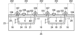
- FIG. 1 is a sectional view schematically showing an example of a configuration of a semiconductor device according to the present embodiment.
- the semiconductor device includes a diamond substrate 23 made of diamond, an epitaxial semiconductor layer 2 which is a nitride semiconductor layer formed inside a concave portion 17 of the diamond substrate 23, and an epitaxial semiconductor layer 2.
- a source or drain electrode metal 101 partially formed on the upper surface 401 of the epitaxial semiconductor layer 3, and a drain or a drain electrode partially formed on the upper surface 401 of the epitaxial semiconductor layer 3.
- Protective film 105 and upper surface of source or drain electrode metal 101 Comprises a source or drain pad electrode metal 107 is partially covered by forming, the drain or the source pad electrode metal 108 of the upper surface is formed partially cover the drain or source electrode metal 102.
- the diamond substrate 23 has an upper surface 109 and a lower surface 25.
- the convex portion 16 is formed on the upper surface 109 of the diamond substrate 23, and the concave portion 17 surrounded on all sides by the convex portion 16 in plan view is provided with a GaN or AlN-based material (hereinafter, referred to as a nitride-based semiconductor material).
- the epitaxial semiconductor layer 2 and the epitaxial semiconductor layer 3 are filled.
- the concave portion 17 may not be surrounded by the convex portion 16 in plan view. That is, for example, the concave portion 17 may have a stripe structure extending in the front and back directions of the drawing (the same applies to the following embodiments).
- the material of the epitaxial semiconductor layer 2 and the epitaxial semiconductor layer 3 includes, for example, Si, GaAs, SiC, or Ga 2 O 3 .
- the epitaxial semiconductor layer 2 and the epitaxial semiconductor layer 3 are stacked, but a single epitaxial semiconductor layer may be formed in the recess 17.
- the field effect transistor 201 is formed on the upper surface 401 of the epitaxial semiconductor layer 3.
- the field-effect transistor is, for example, a metal-insulator-semiconductor (MIS) type field-effect transistor, a metal-oxide-semiconductor (metal-oxide-semiconductor, or MOS).
- MIS metal-insulator-semiconductor
- MOS metal-oxide-semiconductor
- a horizontal semiconductor device such as a field-effect transistor or a high electron mobility transistor (HEMT).
- HEMT high electron mobility transistor
- the upper surface 401 of the epitaxial semiconductor layer 3 is located on the same plane as the upper surface 109 of the diamond substrate 23.
- the HEMT device formed on the upper surface 401 of the epitaxial semiconductor layer 3 includes a source or drain electrode metal 101, a drain or source electrode metal 102, and a gate electrode metal 106.
- the HEMT device formed on the upper surface 401 of the epitaxial semiconductor layer 3 may include a source or drain pad electrode metal 107 and a drain or source pad electrode metal.
- the shape of the gate electrode metal 106 may be any shape suitable for the purpose in the present embodiment. Further, a field plate electrode metal may be formed on the upper surface of the gate electrode metal 106.
- At least one layer of the surface protection film 105 is formed on the upper surface 401 of the epitaxial semiconductor layer 3 in the region where the electrode is not formed.
- the surface protective film 105 has a function of controlling an electric field or controlling a surface potential, and further has a function of inactivating a surface state, water resistance, or moisture resistance.
- a part of the gate electrode metal 106 may not be formed to cover a part of the surface protection film 105.
- an element isolation region 202 exists in a gap between the adjacent field effect transistors 201.
- the element isolation region 202 is formed on the projection 16 on the upper surface 109 of the diamond substrate.
- the diamond substrate 23 which is a material having a high thermal conductivity, surrounds the four sides of the field effect transistor 201 in a plan view.
- the semiconductor device according to the present embodiment exhibits high heat dissipation efficiency because the high thermal conductivity material surrounds the four sides of the active region in plan view.
- the epitaxial semiconductor layer 2 and the diamond substrate 23 are in direct contact with each other to form the bonding interface 28, the influence of the interface thermal resistance is small. Therefore, heat can be dissipated seamlessly (that is, in a state where there is no seam).
- diamond is generally a material with high electrical insulation. Therefore, when the electrical resistivity of the diamond substrate 23 applied in the present embodiment is sufficiently higher than at least the electrical resistivity of the epitaxial semiconductor layer 2 or the electrical resistivity of the epitaxial semiconductor layer 3, the convex portions of the diamond substrate 23 are formed. 16 can exhibit the function of separating elements.
- an element separation step is usually required, and a two-dimensional electron gas serving as a carrier is physically eliminated by a dry etching process, or an element isolation region is equivalent to a selective ion implantation process.
- a technique of physically destroying the epitaxial semiconductor crystal in the region to be formed is adopted.
- the epitaxial semiconductor layer 2 is in direct contact with the diamond substrate 23, but in the present embodiment, a configuration in which the epitaxial semiconductor layer 2 and the diamond substrate 23 are not in direct contact will be described.
- FIG. 2 is a sectional view schematically showing an example of the configuration of the semiconductor device according to the present embodiment.
- the semiconductor device includes a diamond substrate 23, an adhesion layer or nucleation layer 19 formed to cover the inner walls of the projections 16 and the depressions 17 of the diamond substrate 23, and an adhesion layer or nucleus.
- the diamond substrate 23 forms the bonding interface 24 by directly contacting the adhesion layer or the nucleation layer 19.
- the epitaxial semiconductor layer 2 forms a bonding interface 21 by directly contacting the adhesion layer or the nucleation layer 19.
- an amorphous material such as amorphous Si or Si nitride is generally used.
- a crystalline material may be used as the material of the adhesion layer or the nucleation layer 19.
- diamond nanoparticles called diamond seeds may be used as the material of the adhesion layer or the nucleation layer 19.
- the thickness of the adhesion layer or the nucleation layer 19 is desirably, for example, 50 nm or less.
- the adhesion layer or the nucleation layer 19 is interposed between the diamond substrate 23 and the epitaxial semiconductor layer 2, the film is peeled between the diamond substrate 23 and the epitaxial semiconductor layer 2. , Defects or cracks can be prevented from entering. Therefore, the adhesion of the joining between different materials can be improved.
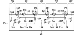
- FIG. 3 is a sectional view schematically showing another example of the configuration of the semiconductor device according to the present embodiment.
- the configuration illustrated in FIG. 3 differs from the configuration illustrated in FIGS. 1 and 2 in that the position of the protrusion 16 ⁇ / b> A does not correspond to the inter-element isolation region 202. That is, in the configuration illustrated in FIG. 3, the width of the concave portion 17A of the diamond substrate 23A is narrow, that is, the width of the convex portion 16A of the diamond substrate 23A is wide.
- the protrusion 16A is formed to extend directly below the source or drain electrode metal 101 adjacent to the protrusion 16A and directly below the drain or source electrode metal 102.
- the semiconductor device includes a diamond substrate 23A, an adhesion layer or nucleation layer 19A formed to cover the projections 16A and the depressions 17A of the diamond substrate 23A, Epitaxial semiconductor layer 2A formed in concave portion 17A of diamond substrate 23A covered with 19A, epitaxial semiconductor layer 3A formed on the upper surface of epitaxial semiconductor layer 2A, and convex portion covered with adhesion layer or nucleation layer 19A.
- the adhesion layer or the nucleation layer 19A may not be formed.
- the diamond substrate 23A forms a bonding interface 24A by directly contacting the adhesion layer or the nucleation layer 19A.
- the epitaxial semiconductor layer 2A forms a bonding interface 21A by directly contacting the adhesion layer or the nucleation layer 19A.
- the diamond substrate 23A which is a material having a high thermal conductivity, surrounds the four sides of the field effect transistor 201 in a plan view at a closer distance.
- the semiconductor device according to the present embodiment exhibits high heat dissipation efficiency because the high thermal conductivity material surrounds the four sides of the active region in plan view.
- a microwave monolithic integrated circuit (MMIC) used in a microwave communication system, a millimeter wave communication system, or the like is configured by a HEMT device.
- a multi-finger HEMT in which a plurality of unit HEMTs are electrically connected in parallel is employed as a HEMT device used for a high output power amplifier of the MMIC.
- the heat generated by the unit HEMTs connected in parallel to each other is an amount that cannot be ignored.
- the unit HEMT device located near the center of the multi-finger type HEMT concentrates heat under the influence of the heat generated from the unit HEMT device located therearound, so that the heat radiation efficiency deteriorates. As a result, the unit HEMT device located near the center of the multi-finger HEMT is easily broken.
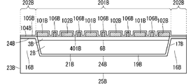
- FIG. 4 is a sectional view schematically showing an example of the configuration of the semiconductor device according to the present embodiment.
- the semiconductor device whose example is shown in FIG. 4 is a multi-finger field effect transistor in which a plurality of field effect transistors are electrically connected in parallel.
- the unit field effect transistors connected in parallel may be, for example, MIS type, MOS type, or HEMT devices.
- a multi-finger HEMT is shown as an example.
- the semiconductor device includes a diamond substrate 23B, an epitaxial semiconductor layer 2B formed in a concave portion 17B of the diamond substrate 23B, and an epitaxial semiconductor layer 3B formed on an upper surface of the epitaxial semiconductor layer 2B.
- a source or drain electrode metal 101B partially formed on the upper surface 401B of the epitaxial semiconductor layer 3B; a drain or source electrode metal 102B partially formed on the upper surface 401B of the epitaxial semiconductor layer 3B;
- the semiconductor device includes a gate electrode metal 106B partially formed on the upper surface 401B, an upper surface 401B of the epitaxial semiconductor layer 3B, and a surface protection film 105B formed to cover the upper surface 109B of the projection 16B.
- the diamond substrate 23B has an upper surface 109B and a lower surface 25B.
- the convex portion 16B is formed on the upper surface 109B of the diamond substrate 23B, and the concave portion 17B surrounded on all sides by the convex portion 16B in plan view is filled with the epitaxial semiconductor layer 2B and the epitaxial semiconductor layer 3B.
- the material of the epitaxial semiconductor layer 2B and the epitaxial semiconductor layer 3B includes, for example, Si, GaAs, SiC, Ga 2 O 3, or the like.
- the epitaxial semiconductor layer 2B and the epitaxial semiconductor layer 3B are stacked, but a single epitaxial semiconductor layer may be formed in the recess 17B.
- a multi-finger HEMT 201B is formed on the upper surface 401B of the epitaxial semiconductor layer 3B.
- the unit HEMT including the source or drain electrode metal 101B, the drain or source electrode metal 102B, and the gate electrode metal 106B includes a drain wiring, a gate wiring, They are electrically connected in parallel by source wiring.
- the shape of the gate electrode metal 106B may be any shape suitable for the purpose in the present embodiment. Further, a field plate electrode metal may be formed on the upper surface of the gate electrode metal 106B.
- any number of unit HEMT devices may be connected in parallel.
- At least one surface protection film 105B is formed on the upper surface 401B of the epitaxial semiconductor layer 3B in the region where the electrode is not formed and on each electrode.
- the surface protective film 105B has a function of controlling an electric field or controlling a surface potential, and further has a function of inactivating a surface state, water resistance, or moisture resistance.
- the diamond substrate 23B which is a material having a high thermal conductivity, surrounds the four sides of the multi-finger HEMT 201B in plan view.
- the semiconductor device according to the present embodiment exhibits high heat dissipation efficiency because the high thermal conductivity material surrounds the four sides of the active region in plan view. Further, since the epitaxial semiconductor layer 2B and the diamond substrate 23B are in direct contact with each other to form the bonding interface 28B, the influence of the interface thermal resistance is small. Therefore, heat can be dissipated seamlessly (that is, in a state where there is no seam).
- diamond is generally a material with high electrical insulation. Therefore, when the electrical resistivity of the diamond substrate 23B applied in the present embodiment is sufficiently higher than at least the electrical resistivity of the epitaxial semiconductor layer 2B or the electrical resistivity of the epitaxial semiconductor layer 3B, the convex portions of the diamond substrate 23B are formed. 16B can exhibit the function of separating elements.
- an element separation step is usually required, and a two-dimensional electron gas serving as a carrier is physically eliminated by a dry etching process, or an element isolation region is equivalent to a selective ion implantation process.
- a technique of physically destroying the epitaxial semiconductor crystal in the region to be formed is adopted.
- FIG. 5 is a sectional view schematically showing an example of the configuration of the semiconductor device according to the present embodiment.
- the semiconductor device includes a diamond substrate 23B, an adhesion layer or nucleation layer 19B formed to cover the projections 16B and the depressions 17B of the diamond substrate 23B, and an adhesion layer or nucleation layer.
- a protective film 105B is a protective film 105B.
- the diamond substrate 23B forms a bonding interface 24B by directly contacting the adhesion layer or the nucleation layer 19B.
- the epitaxial semiconductor layer 2B forms a bonding interface 21B by directly contacting the adhesion layer or the nucleation layer 19B.
- an amorphous material such as amorphous Si or Si nitride is generally used.
- a crystalline material may be used as the material of the adhesion layer or the nucleation layer 19B.
- diamond nanoparticles may be used as the material of the adhesion layer or the nucleation layer 19B.
- the thickness of the adhesion layer or the nucleation layer 19B is desirably, for example, 50 nm or less.
- the adhesion layer or the nucleation layer 19B is interposed between the diamond substrate 23B and the epitaxial semiconductor layer 2B, so that the film is peeled between the diamond substrate 23B and the epitaxial semiconductor layer 2B. , Defects or cracks can be prevented from entering. Therefore, the adhesion of the joining between different materials can be improved.
- FIG. 6 is a sectional view schematically showing another example of the configuration of the semiconductor device according to the present embodiment.
- the configuration illustrated in FIG. 6 differs from the configuration illustrated in FIGS. 4 and 5 in that the position of the protrusion 16C does not correspond to the element isolation region 202B. That is, in the configuration illustrated in FIG. 6, the width of the concave portion 17C of the diamond substrate 23C is small, and a plurality of the concave portions 17C are formed between the adjacent convex portions 16C.
- the protrusion 16C is formed to extend directly below the source or drain electrode metal 101B adjacent to the protrusion 16C and directly below the drain or source electrode metal 102B.
- the semiconductor device includes a diamond substrate 23C, an adhesion layer or nucleation layer 19C formed to cover the projections 16C and the depressions 17C of the diamond substrate 23C, The epitaxial semiconductor layer 2C formed in the concave portion 17C of the diamond substrate 23C covered with 19C, the epitaxial semiconductor layer 3C formed on the upper surface of the epitaxial semiconductor layer 2C, and the convex portion covered with the adhesion layer or the nucleation layer 19C.
- a source or drain electrode metal 101B partially formed on the upper surface of the protrusion 16C and formed on the upper surface of the protrusion 16D between the plurality of recesses 17C formed between the adjacent protrusions 16C; Partially formed on the upper surface of the convex portion 16C covered with the formation layer 19C, and on the convex portion 16D between the plurality of concave portions 17C.
- the gate electrode metal 106B partially formed on the upper surface 401C of the epitaxial semiconductor layer 3C, the upper surface 401C of the epitaxial semiconductor layer 3C, and the upper surface of the protrusion 16C.
- a surface protection film 105B to be formed.
- the adhesion layer or the nucleation layer 19C may not be formed.
- the diamond substrate 23C forms a bonding interface 24C by directly contacting the adhesion layer or the nucleation layer 19C.
- the epitaxial semiconductor layer 2C forms a bonding interface 21C by directly contacting the adhesion layer or the nucleation layer 19C.
- the diamond substrate 23C which is a material having a high thermal conductivity, surrounds the four sides of the multi-finger HEMT 201B in a plan view at a closer distance.
- the heat is generated in the active region of the multi-finger HEMT 201B, and is particularly concentrated on the center of the multi-finger HEMT 201B. Therefore, the semiconductor device according to the present embodiment exhibits high heat dissipation efficiency because the high thermal conductivity material surrounds the four sides of the active region in plan view.
- FIG. 7 is a flowchart illustrating an example of a method of manufacturing the semiconductor device according to the embodiment described above.
- 9 to 17 are cross-sectional views illustrating an example of a manufacturing process of the semiconductor device according to the present embodiment.
- a method for manufacturing a semiconductor device according to the present embodiment will be described with reference to FIGS. 7 and 9 to 17.
- a GaN-on-Si substrate 303 in which a GaN layer 302 is formed on the upper surface of a Si substrate 301 is prepared as a starting substrate for manufacturing processing (for example, see FIG. 9).
- the GaN-on-Si substrate 303 is given as an example of the starting substrate in the manufacturing method according to the present embodiment, the starting substrate is, for example, a GaN-on-sapphire substrate or a GaN-on-SiC substrate. There may be.
- a support substrate 305 is attached to the surface of the GaN layer 302 of the GaN-on-Si substrate 303 (for example, see FIG. 10).
- the support substrate 305 for example, a Si substrate, a sapphire substrate, a quartz substrate, or the like is used.
- the GaN surface is previously planarized so that the arithmetic average roughness (Ra) is 30 nm or less. The same applies to the attachment surface of the support substrate 305.
- a bonding method such as a hydrophilic bonding method, a pressure bonding method, or a plasma activated bonding method may be used.
- an adhesive method using an inorganic adhesive material or the like may be used.
- an arbitrary interlayer film may be provided on the bonding surface between the support substrate 305 and the surface of the GaN layer 302 of the GaN-on-Si substrate 303.
- a material of the interlayer film for example, a material generally used as a semiconductor protective film, such as a silicon nitride or alumina film, is desirably used.
- a composite substrate in which the support substrate 305 and the surface of the GaN layer 302 are joined can be manufactured.
- step ST303 a hard mask 306 is formed on the surface of the starting substrate Si substrate 301 in the composite substrate in which the supporting substrate 305 and the surface of the GaN layer 302 of the GaN-on-Si substrate 303 are joined ( For example, see FIG. 11).
- the hard mask 306 is desirably a material having dry etching resistance and having an etching selectivity with respect to Si or GaN.
- the material of the hard mask 306 may be, for example, Si nitride, an alumina film, or Si dioxide.
- PVD physical vapor deposition
- CVD chemical vapor deposition
- the hard mask 306 may be formed in one or more layers in accordance with the respective selection ratios in the step of forming the through groove after step ST304.
- step ST304 a resist pattern for forming a through groove is formed on the hard mask 306 formed in step ST303.
- the resist pattern for the through groove must be formed so as to surround four sides of a region constituting the semiconductor device according to the present embodiment in plan view.
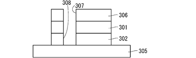
- an opening region 307 that forms a through groove is a region where the hard mask 306 is exposed to an external environment, while a non-open region that is a region other than the opening region 307 where a through groove is formed is This is a region where the hard mask 306 is protected by the resist.
- step ST305 only the hard mask 306 corresponding to the opening region 307 exposed to the external environment is removed (for example, see FIG. 12).
- a method of removing the hard mask 306 for example, wet etching by immersion in a chemical solution or dry etching is selected.
- the surface of the Si substrate 301 in the opening region 307 is further exposed to the external environment. Thereafter, the resist pattern is peeled off from the hard mask 306, so that the hard mask 306 corresponding to the non-opening region is exposed to the external environment.
- step ST306 only the Si substrate 301 in the opening region 307 exposed to the external environment is removed (for example, see FIG. 13).
- the Si substrate 301 having a thickness of several hundred ⁇ m is partially removed.
- the GaN layer 302 corresponding to the opening region 307 is exposed to the external environment.
- the hard mask 306 is not allowed to be completely removed during step ST306.
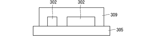
- step ST307 only the GaN layer 302 corresponding to the opening region 307 exposed to the external environment is removed (for example, see FIG. 14).
- the GaN layer 302 corresponding to a thickness of several ⁇ m or more and several tens ⁇ m or less is partially removed.
- the bonding surface of the region corresponding to the opening region 307 with the support substrate 305 is exposed to the external environment.
- the hard mask 306 is not allowed to be completely removed during step ST307.
- a through groove 308 is formed in the GaN-on-Si substrate 303.
- the following two effects can be obtained.
- the first effect is that a characteristic semiconductor device structure according to the present embodiment can be formed.
- the second effect is to suppress the occurrence of cracks or cracks in the GaN layer 302 that may occur in the substrate removing step by releasing the stress.
- step ST308 the hard mask 306 in the non-opening region is removed. It is desirable to use a dry etching technique as the technique for removing the hard mask 306 in step ST308.
- Dry etching has anisotropic etching progress.
- the GaN layer 302 and the Si substrate 301 exist on the side surface of the region where the through groove 308 is formed. Then, in order to suppress the progress of the etching for these, a dry etching technique is used.
- step ST309 all of the Si substrate 301 in the non-opening region exposed to the external environment is removed (for example, see FIG. 15).
- the GaN layer 302 is exposed to an external environment after removing the Si substrate 301.
- a planarization process such as chemical mechanical polishing (CMP) or mechanical grinding may be added.
- CMP chemical mechanical polishing
- step ST310 an adhesion layer or a nucleation layer is formed.
- Step ST310 may be omitted.
- the structure of the semiconductor device obtained by omitting step ST310 and the effects produced by the configuration are as described in the first embodiment and the fourth embodiment.
- the adhesion layer or the nucleation layer is formed for the purpose of improving the adhesion when the diamond substrate is grown or bonded in the steps after step ST311.
- an amorphous material such as amorphous Si or Si nitride is generally used.
- diamond nanoparticles, diamond-like carbon, graphene, graphite, or the like having excellent thermal conductivity may be used.
- the adhesion layer or the nucleation layer must also be formed so as to cover the inside of the through groove 308. At this time, in order to flatten the surface of the adhesion layer or the nucleation layer, for example, a flattening process such as CMP or mechanical grinding may be added.
- a diamond layer 309 is formed on the upper surface of the GaN layer 302 and inside the through groove (for example, see FIG. 16).
- a method of forming the diamond layer 309 for example, a vapor phase growth such as a microwave CVD method or a hot filament CVD method using a CH 4 —H 2 —O 2 based gas, or a bonding method with a diamond free-standing substrate is used. Good.
- the film In the case of vapor phase growth, the film must be thick enough to be independent. On the other hand, if the joining method is used, it is necessary to process a free-standing substrate that fits into the through groove 308.
- the GaN layer 302 is formed in the concave portion on the upper surface of the diamond substrate can be manufactured. It is desirable that the diamond to be formed has high electrical insulation. Further, it is desirable that the diamond layer 309 completely fills the inside of the through groove 308 without any void.
- the crystallinity of the formed diamond may be single crystal or polycrystal.
- the heat transport characteristics of the formed diamond are more excellent as the single crystal has a long-range order, it is desirable that the crystal flow be large and have high crystallinity.
- step ST312 the GaN layer 302 and the support substrate 305 are released (for example, see FIG. 17).
- a wet etching method using a chemical solution may be adopted. However, care should be taken that the chemical solution does not impair the structure other than the free part.
- step ST313 the surface of the GaN layer 302 is exposed to the environment.
- a device process such as formation of an electrode on the surface of the GaN layer 302
- the structure of the semiconductor device according to the present embodiment can be manufactured.
- the diamond can fulfill the function of separating elements.
- the element separation step in the device process can be simplified.
- this step can be omitted. Further, by omitting the selective ion implantation process, it is possible to improve the degree of freedom in the process, for example, such as permitting a high-temperature heat history.
- FIG. 8 is a flowchart illustrating another example of a method of manufacturing the semiconductor device illustrated in FIGS. 1 to 6.
- 18 to 23 are cross-sectional views illustrating an example of a manufacturing process of the semiconductor device according to the present embodiment.
- a method for manufacturing a semiconductor device according to the present embodiment will be described with reference to FIG. 8 and FIGS.
- a diamond free-standing substrate 310 is prepared as a starting substrate (for example, see FIG. 18). It is desirable that the self-standing diamond substrate 310 applied in the present embodiment has high electrical insulation. Further, in order to flatten the surface of the diamond free-standing substrate 310, for example, a flattening process such as CMP or mechanical grinding may be added.
- a hard mask 311 is formed on the surface of the diamond free-standing substrate 310 (for example, see FIG. 19).
- the hard mask 311 is desirably a material having dry etching resistance and having a selective ratio of etching to diamond.
- the material of the hard mask 311 may be, for example, Si nitride, an alumina film, or Si dioxide.
- the method of forming these materials may be, for example, a PVD method or a CVD method. Further, the hard mask 311 may have a configuration in which one or more layers are formed.
- a resist pattern for forming a concave portion in the diamond free-standing substrate 310 is formed on the hard mask 311 formed in step ST402.
- the resist pattern for forming the concave portion must be formed so as to surround four sides of a region constituting the semiconductor device according to the present embodiment in plan view.
- an opening region 312 forming a concave portion is a region where the hard mask 311 is exposed to the external environment, while a non-opening region other than the opening region 312 where the concave portion is formed is formed by a resist. This is an area where the hard mask 311 is protected.
- step ST404 only the hard mask 311 corresponding to the opening region 312 exposed to the external environment is removed (for example, see FIG. 20).
- a method for removing the hard mask 311 for example, wet etching by immersion in a chemical solution or dry etching is selected.
- the surface of the free-standing diamond substrate 310 in the opening region 312 is further exposed to the external environment.
- the resist pattern is peeled off from the hard mask 311 so that the hard mask 311 corresponding to the non-opening region is exposed to the external environment.
- step ST405 only the diamond free-standing substrate 310 in the opening region 312 exposed to the external environment is partially removed. Then, a concave portion 313 is formed in a region corresponding to the opening region 312 (see, for example, FIG. 21).
- the method for removing the diamond substrate in the opening region 312 may be any other removal method suitable for the purpose in the present embodiment.
- the removal amount of the diamond free-standing substrate 310 must be properly controlled to a film thickness that matches the dimensions of the semiconductor device to be manufactured. Therefore, it is not assumed that the diamond free-standing substrate 310 is removed through all the opening regions 312.
- the etched surface of the free-standing diamond substrate 310 in the opening region 312, that is, the recess 313 is exposed to the external environment.
- a flattening process such as CMP or mechanical grinding may be added.
- a nitride semiconductor layer 314 is formed on the etched surface of the free-standing diamond substrate 310 exposed to the external environment, that is, on the concave portion 313 (see, for example, FIG. 22).
- a method for forming the nitride semiconductor layer 314 for example, a metal organic chemical vapor deposition (MOCVD) method, a molecular beam epitaxy (MBE) method, or the like is used. You may. Or, J. W.
- a method of crystal growth of a nitride semiconductor on a graphene film reported by Shon et al. (JW Shon, J. Ohta, K. Ueno, A. Kobayashi, and @H.
- the nitride semiconductor layer 314 may be formed of at least one layer.
- a first epitaxial semiconductor layer serving as an electron transit layer and a second epitaxial semiconductor layer serving as a barrier layer are formed to form 2DEG.
- the thickness of the nitride semiconductor layer 314 to be grown must be controlled and must be the same height as the non-etched surface of the diamond free-standing substrate 310.
- a lattice relaxation layer for mitigating lattice mismatch with the semiconductor layer 314 may be interposed.
- the surface of the nitride semiconductor layer 314 in the opening region 312 is exposed to an external environment.
- a flattening process such as CMP or mechanical grinding may be added.
- step ST407 the hard mask 311 on the surface of the free-standing diamond substrate 310, which is a non-opening region, is removed (for example, see FIG. 23).
- the method of removing the hard mask 311 in step ST407 may be wet etching using a chemical solution or dry etching.
- the wet etching removal method has a small influence of damage to the nitride semiconductor layer 314 and easily removes the hard mask 311. it can.
- step ST408 the surface of the nitride semiconductor layer 314 is subjected to a device process such as formation of an electrode, whereby the structure of the semiconductor device according to the present embodiment can be manufactured.
- the diamond having a high electrical insulation surrounds the nitride semiconductor layer 314 on all sides in plan view, so that the diamond free-standing substrate 310 can fulfill a function of separating elements. .
- the element separation step in the device process can be simplified.
- this step can be omitted. Further, by omitting the selective ion implantation process, it is possible to improve the degree of freedom in the process, for example, such as permitting a high-temperature heat history.
- the replacement may be made over a plurality of embodiments. That is, a configuration in which the same effects are obtained by combining the respective configurations illustrated in the different embodiments may be used.
- the semiconductor device includes the diamond substrate 23 made of diamond and the nitride semiconductor layer.
- the nitride semiconductor layers include, for example, epitaxial semiconductor layer 2, epitaxial semiconductor layer 2A, epitaxial semiconductor layer 2B, epitaxial semiconductor layer 2C, epitaxial semiconductor layer 3, epitaxial semiconductor layer 3A, epitaxial semiconductor layer 3B, and epitaxial semiconductor layer 3C.
- the epitaxial semiconductor layer 2 and the epitaxial semiconductor layer 3 are formed inside the concave portion 17 formed on the upper surface 109 of the diamond substrate 23.
- diamond having high thermal conductivity is formed in contact with the side surface as well as the lower surface of the nitride semiconductor layer. Therefore, when an element structure or the like is formed on the upper surface of the nitride semiconductor layer and the semiconductor device including the nitride semiconductor layer becomes a heat source, the semiconductor device exhibits high heat dissipation performance to the side below and in addition to the semiconductor device. Can be. Therefore, the temperature rise of the semiconductor device can be significantly suppressed.
- the epitaxial semiconductor layer 2 and the epitaxial semiconductor layer 3 are formed so as to be entirely surrounded by the upper surface 109 of the diamond substrate 23 in a plan view. According to such a configuration, high heat dissipation performance can be exerted on all sides of the semiconductor device. Therefore, the temperature rise of the semiconductor device can be significantly suppressed.
- the upper surface 109 of the diamond substrate 23 and the upper surface 401 of the epitaxial semiconductor layer 3 are located on the same plane. According to such a configuration, since the sides of the epitaxial semiconductor layer 2 and the sides of the epitaxial semiconductor layer 3 can be covered with the diamond substrate 23 without leakage, high heat radiation performance can be exhibited on the sides of the semiconductor device. it can.
- the diamond substrate 23 has electrical insulation. According to such a configuration, the convex portion 16 of the diamond substrate 23 can be used as an element isolation region of a semiconductor device. Therefore, it is not necessary to separately provide a step for forming an element isolation region, and the manufacturing process can be simplified.
- the semiconductor device includes the intervening layer formed on the inner wall of the concave portion 17 of the diamond substrate 23.
- the intervening layer corresponds to, for example, at least one of the adhesion layer or nucleation layer 19A, the adhesion layer or nucleation layer 19A, the adhesion layer or nucleation layer 19B, and the adhesion layer or nucleation layer 19C. It is.
- the epitaxial semiconductor layer 2 and the epitaxial semiconductor layer 3 are formed inside the concave portion 17 of the diamond substrate 23 via the adhesion layer or the nucleation layer 19.
- the intervening layer is a lattice relaxation layer that mitigates lattice mismatch between the diamond free-standing substrate 310 and the nitride semiconductor layer 314.
- the lattice mismatch can be reduced and the nitride semiconductor layer 314 with few crystal defects can be formed.
- the semiconductor device includes the electrode unit formed on the upper surface of the epitaxial semiconductor layer 3.
- the electrode portion corresponds to, for example, at least one of drain electrode metal 101, drain electrode metal 101B, drain or source electrode metal 102, drain or source electrode metal 102B, gate electrode metal 106, and gate electrode metal 106B. Is what you do. According to such a configuration, when the element structure or the like is formed on the upper surface of the epitaxial semiconductor layer 3 and the semiconductor device becomes a heat source, a high heat radiation performance is exhibited not only below the semiconductor device but also laterally. Can be.
- a nitride semiconductor layer is formed on an upper surface of a semiconductor substrate.
- the semiconductor substrate corresponds to, for example, the Si substrate 301.
- the nitride semiconductor layer corresponds to, for example, the GaN layer 302.
- the surface of the GaN layer 302 and the support substrate 305 are joined.
- a hard mask 306 is formed on the lower surface of the Si substrate 301.
- a pattern having an opening region 307 is formed on the hard mask 306.
- a groove 308 penetrating the Si substrate 301 and the GaN layer 302 is formed.
- the hard mask 306 and the Si substrate 301 are removed.
- a diamond layer 309 covering the GaN layer 302 is formed on the surface of the support substrate 305.
- the surface of the GaN layer 302, the surface of the diamond layer 309, and the support substrate 305 are released.
- the grooves 308 that penetrate the Si substrate 301 and the GaN layer 302 are formed in advance, so that the stress relaxation in the GaN layer 302 is achieved.
- the generation of cracks or cracks due to the above can be suppressed.
- a diamond substrate made of diamond is prepared.
- the diamond substrate corresponds to the diamond free-standing substrate 310, for example.
- a hard mask 311 is formed on the surface of the diamond free-standing substrate 310.
- a pattern having an opening region 312 is formed on the hard mask 311.
- the concave portion 313 is formed by removing the diamond free-standing substrate 310 corresponding to the opening region 312.
- a nitride semiconductor layer 314 is epitaxially grown inside the recess 313.
- the semiconductor device according to the present embodiment can be easily manufactured commercially.
- the step of commercially removing the diamond free-standing substrate 310 is realized, commercial production of the semiconductor device according to the present embodiment can be easily performed.
- each component in the embodiment described above is a conceptual unit, and one component includes a plurality of structures within the scope of the technology disclosed in this specification. And a case where one component corresponds to a part of a structure, and a case where a plurality of components are provided in one structure.
- each component in the above-described embodiment includes a structure having another structure or shape as long as the same function is exhibited.
- the material includes other additives, such as an alloy. Shall be included.
Landscapes
- Junction Field-Effect Transistors (AREA)
- Insulated Gate Type Field-Effect Transistor (AREA)
- Physical Vapour Deposition (AREA)
- Chemical Vapour Deposition (AREA)
Abstract
Description
以下、本実施の形態に関する半導体装置、および、半導体装置の製造方法について説明する。
図1は、本実施の形態に関する半導体装置の構成の例を概略的に示す断面図である。図1に例が示されるように、半導体装置は、ダイヤモンドからなるダイヤモンド基板23と、ダイヤモンド基板23の凹部17の内部に形成される窒化物半導体層であるエピタキシャル半導体層2と、エピタキシャル半導体層2の上面に形成されるエピタキシャル半導体層3と、エピタキシャル半導体層3の上面401に部分的に形成されるソースまたはドレイン電極金属101と、エピタキシャル半導体層3の上面401に部分的に形成されるドレインまたはソース電極金属102と、エピタキシャル半導体層3の上面401に部分的に形成されるゲート電極金属106と、凸部16の上面109およびエピタキシャル半導体層3の上面401を部分的に覆って形成される表面保護膜105と、ソースまたはドレイン電極金属101の上面を部分的に覆って形成されるソースまたはドレインパッド電極金属107と、ドレインまたはソース電極金属102の上面を部分的に覆って形成されるドレインまたはソースパッド電極金属108とを備える。
本実施の形態に関する半導体装置、および、半導体装置の製造方法について説明する。以下の説明においては、以上に記載された実施の形態で説明された構成要素と同様の構成要素については同じ符号を付して図示し、その詳細な説明については適宜省略するものとする。
図1においては、エピタキシャル半導体層2とダイヤモンド基板23とが直接接触していたが、本実施の形態では、エピタキシャル半導体層2とダイヤモンド基板23とが直接接触していない構成について説明する。
本実施の形態に関する半導体装置、および、半導体装置の製造方法について説明する。以下の説明においては、以上に記載された実施の形態で説明された構成要素と同様の構成要素については同じ符号を付して図示し、その詳細な説明については適宜省略するものとする。
図3は、本実施の形態に関する半導体装置の構成の別の例を概略的に示す断面図である。図3に例が示される構成は、図1および図2に例が示された構成とは異なり、凸部16Aの位置が素子間分離領域202には対応していない。つまり、図3に例が示される構成は、ダイヤモンド基板23Aの凹部17Aの幅が狭い、すなわち、ダイヤモンド基板23Aの凸部16Aの幅が広い。そして、凸部16Aは、凸部16Aに隣接するソースまたはドレイン電極金属101の直下、および、ドレインまたはソース電極金属102の直下にまで延びて形成される。
本実施の形態に関する半導体装置、および、半導体装置の製造方法について説明する。以下の説明においては、以上に記載された実施の形態で説明された構成要素と同様の構成要素については同じ符号を付して図示し、その詳細な説明については適宜省略するものとする。
マイクロ波通信システム、または、ミリ波通信システムなどに用いられるマイクロ波モノリシック集積回路(monolithic microwave integrated circuit、すなわち、MMIC)は、HEMTデバイスによって構成されている。
本実施の形態に関する半導体装置、および、半導体装置の製造方法について説明する。以下の説明においては、以上に記載された実施の形態で説明された構成要素と同様の構成要素については同じ符号を付して図示し、その詳細な説明については適宜省略するものとする。
図4においては、エピタキシャル半導体層2Bとダイヤモンド基板23Bとが直接接触していたが、本実施の形態では、エピタキシャル半導体層2Bとダイヤモンド基板23Bとが直接接触していない構成について説明する。
本実施の形態に関する半導体装置、および、半導体装置の製造方法について説明する。以下の説明においては、以上に記載された実施の形態で説明された構成要素と同様の構成要素については同じ符号を付して図示し、その詳細な説明については適宜省略するものとする。
図6は、本実施の形態に関する半導体装置の構成の別の例を概略的に示す断面図である。図6に例が示される構成は、図4および図5に例が示された構成とは異なり、凸部16Cの位置が素子間分離領域202Bには対応していない。つまり、図6に例が示される構成は、ダイヤモンド基板23Cの凹部17Cの幅が狭く、かつ、隣り合う凸部16C間において複数形成されている。そして、凸部16Cは、凸部16Cに隣接するソースまたはドレイン電極金属101Bの直下、および、ドレインまたはソース電極金属102Bの直下にまで延びて形成される。
本実施の形態に関する半導体装置、および、半導体装置の製造方法について説明する。以下の説明においては、以上に記載された実施の形態で説明された構成要素と同様の構成要素については同じ符号を付して図示し、その詳細な説明については適宜省略するものとする。
図7は、以上に記載された実施の形態における半導体装置の、製造方法の例を示すフローチャートである。また、図9から図17は、本実施の形態に関する半導体装置の、製造工程の例を示す断面図である。以下、図7および図9から図17を参照しつつ、本実施の形態に関する半導体装置の製造方法を説明する。
本実施の形態に関する半導体装置、および、半導体装置の製造方法について説明する。以下の説明においては、以上に記載された実施の形態で説明された構成要素と同様の構成要素については同じ符号を付して図示し、その詳細な説明については適宜省略するものとする。
図8は、図1から図6に例が示された半導体装置の、製造方法の別の例を示すフローチャートである。また、図18から図23は、本実施の形態に関する半導体装置の、製造工程の例を示す断面図である。以下、図8および図18から図23を参照しつつ、本実施の形態に関する半導体装置の製造方法を説明する。
次に、以上に記載された実施の形態によって生じる効果の例を示す。なお、以下の説明においては、以上に記載された実施の形態に例が示された具体的な構成に基づいて当該効果が記載されるが、同様の効果が生じる範囲で、本願明細書に例が示される他の具体的な構成と置き換えられてもよい。
以上に記載された実施の形態では、それぞれの構成要素の材質、材料、寸法、形状、相対的配置関係または実施の条件などについても記載する場合があるが、これらはすべての局面においてひとつの例であって、本願明細書に記載されたものに限られることはないものとする。
Claims (9)
- ダイヤモンドからなるダイヤモンド基板(23)と、
前記ダイヤモンド基板(23)の上面(109)に形成された凹部(17)の内部に形成される窒化物半導体層(2、3)とを備える、
半導体装置。 - 前記窒化物半導体層(2、3)は、平面視において前記ダイヤモンド基板(23)の前記上面(109)に全周囲を囲まれて形成される、
請求項1に記載の半導体装置。 - 前記ダイヤモンド基板(23)の前記上面(109)と、前記窒化物半導体層(2、3)の上面(401)とが、同一平面上に位置する、
請求項1または請求項2に記載の半導体装置。 - 前記ダイヤモンド基板(23)は、電気絶縁性を有する、
請求項1から請求項3のうちのいずれか1項に記載の半導体装置。 - 前記ダイヤモンド基板(23)の前記凹部(17)の内壁に形成される、介在層(19)をさらに備え、
前記窒化物半導体層(2、3)は、前記介在層(19)を介して前記ダイヤモンド基板(23)の前記凹部(17)の内部に形成される、
請求項1から請求項4のうちのいずれか1項に記載の半導体装置。 - 前記介在層(19)は、前記ダイヤモンド基板(23)と前記窒化物半導体層(2、3)との間の格子不整合を緩和する格子緩和層である、
請求項5に記載の半導体装置。 - 前記窒化物半導体層(2、3)の上面に形成される電極部(101、102、106)をさらに備える、
請求項1から請求項6のうちのいずれか1項に記載の半導体装置。 - 半導体基板(301)の上面に窒化物半導体層(302)を形成し、
前記窒化物半導体層(302)の表面と支持基板(305)とを接合し、
前記半導体基板(301)の下面にハードマスク(306)を形成し、
前記ハードマスク(306)に開口領域(307)を有するパターンを形成し、
前記開口領域(307)に対応する前記半導体基板(301)、さらには、前記窒化物半導体層(302)を除去することによって、前記半導体基板(301)および前記窒化物半導体層(302)を貫通する溝(308)を形成し、
前記ハードマスク(306)および前記半導体基板(301)を除去し、
前記支持基板(305)の表面に、前記窒化物半導体層(302)を覆うダイヤモンド層(309)を形成し、
前記窒化物半導体層(302)の表面および前記ダイヤモンド層(309)の表面と、前記支持基板(305)とを遊離させる、
半導体装置の製造方法。 - ダイヤモンドからなるダイヤモンド基板(310)を用意し、
前記ダイヤモンド基板(310)の表面にハードマスク(311)を形成し、
前記ハードマスク(311)に開口領域(312)を有するパターンを形成し、
前記開口領域(312)に対応する前記ダイヤモンド基板(310)を除去することによって凹部(313)を形成し、
前記凹部(313)の内部に窒化物半導体層(314)をエピタキシャル成長させる、
半導体装置の製造方法。
Priority Applications (4)
| Application Number | Priority Date | Filing Date | Title |
|---|---|---|---|
| JP2020526804A JP6942253B2 (ja) | 2018-06-28 | 2018-06-28 | 半導体装置、および、半導体装置の製造方法 |
| PCT/JP2018/024584 WO2020003436A1 (ja) | 2018-06-28 | 2018-06-28 | 半導体装置、および、半導体装置の製造方法 |
| US16/978,191 US11482464B2 (en) | 2018-06-28 | 2018-06-28 | Semiconductor device including a diamond substrate and method of manufacturing the semiconductor device |
| GB2020038.2A GB2589484B (en) | 2018-06-28 | 2018-06-28 | Semiconductor device and method of manufacturing semiconductor device |
Applications Claiming Priority (1)
| Application Number | Priority Date | Filing Date | Title |
|---|---|---|---|
| PCT/JP2018/024584 WO2020003436A1 (ja) | 2018-06-28 | 2018-06-28 | 半導体装置、および、半導体装置の製造方法 |
Publications (1)
| Publication Number | Publication Date |
|---|---|
| WO2020003436A1 true WO2020003436A1 (ja) | 2020-01-02 |
Family
ID=68986765
Family Applications (1)
| Application Number | Title | Priority Date | Filing Date |
|---|---|---|---|
| PCT/JP2018/024584 Ceased WO2020003436A1 (ja) | 2018-06-28 | 2018-06-28 | 半導体装置、および、半導体装置の製造方法 |
Country Status (4)
| Country | Link |
|---|---|
| US (1) | US11482464B2 (ja) |
| JP (1) | JP6942253B2 (ja) |
| GB (1) | GB2589484B (ja) |
| WO (1) | WO2020003436A1 (ja) |
Cited By (3)
| Publication number | Priority date | Publication date | Assignee | Title |
|---|---|---|---|---|
| KR20220085685A (ko) * | 2020-12-14 | 2022-06-22 | 한국전자통신연구원 | 방열기판, 방열기판의 제조방법, 및 이를 포함하는 반도체 집적 장치 |
| JP2023032650A (ja) * | 2021-08-27 | 2023-03-09 | 住友電気工業株式会社 | 半導体装置 |
| US12191227B2 (en) | 2020-12-14 | 2025-01-07 | Electronics And Telecommunications Research Institute | Heat dissipating substrate comprising diamond and semiconductor integrated device including the same |
Families Citing this family (1)
| Publication number | Priority date | Publication date | Assignee | Title |
|---|---|---|---|---|
| CN115812254A (zh) * | 2020-10-30 | 2023-03-17 | 华为技术有限公司 | 一种半导体器件及其制造方法 |
Citations (6)
| Publication number | Priority date | Publication date | Assignee | Title |
|---|---|---|---|---|
| JP2007096130A (ja) * | 2005-09-29 | 2007-04-12 | Toshiba Corp | 半導体発光素子およびその製造方法 |
| JP2012084653A (ja) * | 2010-10-08 | 2012-04-26 | Advanced Power Device Research Association | 半導体装置およびその製造方法 |
| JP2012084781A (ja) * | 2010-10-14 | 2012-04-26 | National Institute For Materials Science | 電界効果トランジスタ及びその製造方法 |
| JP2015065233A (ja) * | 2013-09-24 | 2015-04-09 | 三菱電機株式会社 | 半導体装置及びその製造方法 |
| JP2016139695A (ja) * | 2015-01-27 | 2016-08-04 | 株式会社東芝 | 半導体装置 |
| JP2018041785A (ja) * | 2016-09-06 | 2018-03-15 | 富士通株式会社 | 半導体装置及び半導体装置の製造方法 |
Family Cites Families (8)
| Publication number | Priority date | Publication date | Assignee | Title |
|---|---|---|---|---|
| JPH11283994A (ja) | 1998-03-30 | 1999-10-15 | Toshiba Corp | マルチフィンガー型電界効果トランジスタ |
| US6956250B2 (en) | 2001-02-23 | 2005-10-18 | Nitronex Corporation | Gallium nitride materials including thermally conductive regions |
| US7846767B1 (en) * | 2007-09-06 | 2010-12-07 | Chien-Min Sung | Semiconductor-on-diamond devices and associated methods |
| JP2009166160A (ja) * | 2008-01-15 | 2009-07-30 | Sumitomo Electric Ind Ltd | 放熱基板の製造方法および放熱基板 |
| US8575657B2 (en) | 2012-03-20 | 2013-11-05 | Northrop Grumman Systems Corporation | Direct growth of diamond in backside vias for GaN HEMT devices |
| US9685513B2 (en) * | 2012-10-24 | 2017-06-20 | The United States Of America, As Represented By The Secretary Of The Navy | Semiconductor structure or device integrated with diamond |
| US9196703B2 (en) * | 2013-08-22 | 2015-11-24 | Northrop Grumman Systems Corporation | Selective deposition of diamond in thermal vias |
| WO2015171873A1 (en) * | 2014-05-07 | 2015-11-12 | Cambridge Electronics, Inc. | Transistor structure having buried island regions |
-
2018
- 2018-06-28 WO PCT/JP2018/024584 patent/WO2020003436A1/ja not_active Ceased
- 2018-06-28 JP JP2020526804A patent/JP6942253B2/ja active Active
- 2018-06-28 GB GB2020038.2A patent/GB2589484B/en active Active
- 2018-06-28 US US16/978,191 patent/US11482464B2/en active Active
Patent Citations (6)
| Publication number | Priority date | Publication date | Assignee | Title |
|---|---|---|---|---|
| JP2007096130A (ja) * | 2005-09-29 | 2007-04-12 | Toshiba Corp | 半導体発光素子およびその製造方法 |
| JP2012084653A (ja) * | 2010-10-08 | 2012-04-26 | Advanced Power Device Research Association | 半導体装置およびその製造方法 |
| JP2012084781A (ja) * | 2010-10-14 | 2012-04-26 | National Institute For Materials Science | 電界効果トランジスタ及びその製造方法 |
| JP2015065233A (ja) * | 2013-09-24 | 2015-04-09 | 三菱電機株式会社 | 半導体装置及びその製造方法 |
| JP2016139695A (ja) * | 2015-01-27 | 2016-08-04 | 株式会社東芝 | 半導体装置 |
| JP2018041785A (ja) * | 2016-09-06 | 2018-03-15 | 富士通株式会社 | 半導体装置及び半導体装置の製造方法 |
Cited By (5)
| Publication number | Priority date | Publication date | Assignee | Title |
|---|---|---|---|---|
| KR20220085685A (ko) * | 2020-12-14 | 2022-06-22 | 한국전자통신연구원 | 방열기판, 방열기판의 제조방법, 및 이를 포함하는 반도체 집적 장치 |
| KR102687720B1 (ko) * | 2020-12-14 | 2024-07-25 | 한국전자통신연구원 | 방열기판, 방열기판의 제조방법, 및 이를 포함하는 반도체 집적 장치 |
| US12191227B2 (en) | 2020-12-14 | 2025-01-07 | Electronics And Telecommunications Research Institute | Heat dissipating substrate comprising diamond and semiconductor integrated device including the same |
| JP2023032650A (ja) * | 2021-08-27 | 2023-03-09 | 住友電気工業株式会社 | 半導体装置 |
| JP7739850B2 (ja) | 2021-08-27 | 2025-09-17 | 住友電気工業株式会社 | 半導体装置 |
Also Published As
| Publication number | Publication date |
|---|---|
| JPWO2020003436A1 (ja) | 2021-01-07 |
| GB2589484B (en) | 2022-09-28 |
| US20210043539A1 (en) | 2021-02-11 |
| US11482464B2 (en) | 2022-10-25 |
| JP6942253B2 (ja) | 2021-09-29 |
| GB202020038D0 (en) | 2021-02-03 |
| GB2589484A (en) | 2021-06-02 |
Similar Documents
| Publication | Publication Date | Title |
|---|---|---|
| JP7217808B2 (ja) | 半導体装置の製造方法 | |
| US9685513B2 (en) | Semiconductor structure or device integrated with diamond | |
| TWI517383B (zh) | 在背側通孔中直接生長鑽石用於GaN高電子遷移率電晶體裝置 | |
| CN103311244B (zh) | 半导体器件及用于制造半导体器件的方法 | |
| JP6942253B2 (ja) | 半導体装置、および、半導体装置の製造方法 | |
| TW201110315A (en) | Monolithic vertically integrated composite group III-V and group IV semiconductor device and method for fabricating same | |
| US11211308B2 (en) | Semiconductor device and manufacturing method thereof | |
| JP2016524819A (ja) | トランジスタ、及び、トランジスタの製造方法 | |
| JP2019153603A (ja) | 半導体基板及びその製造方法 | |
| JP5454283B2 (ja) | 窒化ガリウム系エピタキシャル成長基板及びその製造方法並びにこの基板を用いて製造される電界効果型トランジスタ | |
| JP7052503B2 (ja) | トランジスタの製造方法 | |
| CN111211161A (zh) | 一种双向散热的纵向氮化镓功率晶体管及其制备方法 | |
| JP5487590B2 (ja) | 半導体装置及びその製造方法 | |
| TW201737354A (zh) | 半導體裝置,電子部件,電子設備及用於製造半導體裝置之方法 | |
| CN116325092B (zh) | 半导体器件及其制作方法 | |
| CN112216741A (zh) | 高电子迁移率晶体管的绝缘结构以及其制作方法 | |
| JP5629977B2 (ja) | 半導体装置及びその製造方法 | |
| US10903350B2 (en) | Semiconductor devices and methods for forming the same | |
| CN111223824B (zh) | 半导体装置及其形成方法 | |
| JP2014060427A (ja) | 半導体装置及びその製造方法 | |
| US20180254337A1 (en) | Semiconductor device | |
| GB2603681A (en) | Semiconductor device and method of manufacturing semiconductor device | |
| TWI732155B (zh) | 半導體裝置及其形成方法 | |
| CN117133802B (zh) | 一种半导体器件及其制作方法、封装器件、电子设备 | |
| TW202507808A (zh) | 導熱性提升的分段電晶體主動區 |
Legal Events
| Date | Code | Title | Description |
|---|---|---|---|
| 121 | Ep: the epo has been informed by wipo that ep was designated in this application |
Ref document number: 18923987 Country of ref document: EP Kind code of ref document: A1 |
|
| ENP | Entry into the national phase |
Ref document number: 2020526804 Country of ref document: JP Kind code of ref document: A |
|
| ENP | Entry into the national phase |
Ref document number: 202020038 Country of ref document: GB Kind code of ref document: A Free format text: PCT FILING DATE = 20180628 |
|
| WWE | Wipo information: entry into national phase |
Ref document number: 2204909.2 Country of ref document: GB |
|
| NENP | Non-entry into the national phase |
Ref country code: DE |
|
| 122 | Ep: pct application non-entry in european phase |
Ref document number: 18923987 Country of ref document: EP Kind code of ref document: A1 |
|
| WWD | Wipo information: divisional of initial pct application |
Ref document number: 2204909.2 Country of ref document: GB |
|
| WWG | Wipo information: grant in national office |
Ref document number: 2020038.2 Country of ref document: GB |
|
| WWG | Wipo information: grant in national office |
Ref document number: 2204909.2 Country of ref document: GB |